1
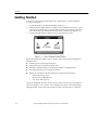
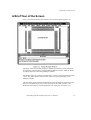
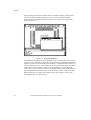
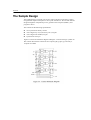
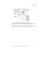
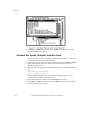
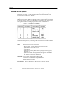
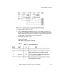
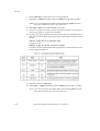
Chapter 3 Tutorial
This tutorial is designed to help you become familiar with the Lattice pLSI 1032
device, the ispLSI 1032 device, and the Lattice pLSI/ispLSI Development System
(pDS). To do this, a complete design of a simple 4-bit counter is discussed from
specification through programming and testing the part. The following assumptions
are made:
■
■
You have read and understood the pLSI 1032 Device Data Sheets
You have the documentation for Microsoft Windows readily available
Windows is an industry-standard Graphic User Interface (GUI) for pull-down menus,
text editing commands, and screen control commands. Because the Lattice interface is
the same as other Windows programs, it is very easy to learn. If you know how to run
any Windows program, you can run the Lattice software.
It is necessary to have Windows 3.1 for the Lattice pDS software to run. Windows
runs on most standard IBM PCs or clones. The recommended system configuration
for running the pDS software includes the following:
■
■
■
■
386 or 486 IBM® PC-AT™ or compatible processor
1 serial port
1 parallel port
8 megabytes of RAM
■
■
■
■
■
pDS software occupies 7MB of disk space
Floppy Disk Drive
Microsoft Windows Compatible Mouse
VGA or Super VGA Graphics (up to 800 X 600)
pDS software security key
The spare parallel printer port is necessary to perform in-system programming and the
spare serial port is necessary to communicate with an RS-232 controlled programmer.
pLSI and ispLSI Development System User Manual
3-1
Tutorial
Getting Started
If you have not previously installed the Lattice pDS software, see the Installation
Procedure in Chapter 1.
1.
2.
3.
To start Windows, type WIN at the DOS prompt (C:>).
Install the Lattice pDS software according to the installation instructions. A new
program group called Lattice is created. This program group should contain three
icons. Select the icon which looks like the Lattice company logo (Figure 3-1).
To start the pDS software, double-click on the Lattice Logo Icon.
Before proceeding any further, learn to perform some of the following Microsoft
Windows tasks:
■
■
■
■
■
Selecting a menu item using the mouse
Using Open, Save, and Save As menu items
Entering commands and text into Message windows and dialog boxes
Moving around the screen with the scroll bars
Editing text using the keyboard and mouse to perform the following:
•
•
•
Select the insertion point
Select text by highlighting it
Cut, paste, and copy text
If you are unfamiliar with any of these options, take some time to go through the
Microsoft Windows User's Guide. For a complete description of the pDS Design
Manager menus, see the pLSI and ispLSI Development System Reference Manual.
3-2
pLSI and ispLSI Development System User Manual
A Brief Tour of the Screen
A Brief Tour of the Screen
Once you invoke the Lattice pDS software, two windows appear (Figure 3-2).
The larger of the two windows displays a graphic representation of the pLSI 1032
logic diagram. This window is called the Design Manager window. Enter the design
by editing equations in the Design Manager window.
The smaller of the two windows is the Messages window, located at the bottom of the
screen. The pDS software communicates with you by placing messages in the
Messages window.
The part that is displayed in the block diagram shows the elements of the pLSI 1032
that can be modified by the user. These elements are the GLBs, the IOCs, the
dedicated input (DI) pins, and the dedicated clock input pins (see Figure 3-2).
pLSI and ispLSI Development System User Manual
3-3
Tutorial
Enter the design into the development software by double-clicking on the box that
you wish to edit and entering equations or macros (library elements already
partitioned and optimized for high performance) into the Edit Cell window that
appears (Figure 3-3).
The method of specifying the logic configuration into a cell depends on what type of
cell it is. Logic configurations for GLBs are entered using a combination of Boolean
equations or macros from the Lattice System Library. Configuration data for IOCs are
entered using macros only. The complete set of macros which describes all possible
combinations of input, output, and IOC logic configurations is contained in the
Lattice Macro Library Reference Manual. Configuration data for the dedicated input
pins and the dedicated clock input pins are entered using a subset of the IOC macros.
Because these pins are inputs only and do not have input registers, many of the
standard IOC macros cannot be used.
3-4
pLSI and ispLSI Development System User Manual
The Design Flow
The Design Flow
Before starting our sample design, it is valuable to understand the design flow.
Observe the following steps to complete a design. Refer to Figure 3-4 for more
information.
pLSI and ispLSI Development System User Manual
3-5
Tutorial
Specify the Design
A design is specified using one of the two approaches. With the first method, you use
an existing design, consisting of 7400 Series TTL Logic elements, and fit the design
into the pLSI part. With the second method, you design a circuit using Boolean
equations or macros that are optimized for best performance and utilization of the
pLSI architecture.
The first approach consists of simply selecting macros from the Lattice library that
approximate the functions of the TTL or CMOS circuits and then connecting them to
each other. Using this approach, a design can be completed quickly and has a high
probability of working the first time because the circuit has been tested.
The second approach ensures better performance and higher utilization, but may
require some circuit redesign. Many designs are a combination of the two approaches.
To select the correct pLSI device, partition the design into GLBs, and count the
number of GLBs and IOCs used. Next, select the pLSI device that can hold the
amount of logic required. Selection of the proper device is based on the amount of
logic required and the number of IOCs needed.
The best utilization and routability are achieved by allowing the software to assign the
I/O pin placement. It is a good idea to design the pLSI part first, and then lay out the
printed circuit board or wire-wrap board after the device has been routed. Once the
software intelligently assigns the pin placement the first time, the pins can be fixed,
and changes can be made to the logic with few problems.
Partition the Logic
Partitioning consists of carving the logic into chunks that conveniently fit into the
pLSI Generic Logic Blocks (GLBs). These general rules should be followed when
partitioning logic:
■
■
■
5-6
Consult the Lattice Macro Library Reference Manual and decide if any of the
logic can be implemented using the standard macros. Macros are already
partitioned and are optimized for high utilization and high performance. Macros
are also the fastest method to input logic into the design.
Know the capabilities of the GLB. For this pLSI 1032 part, there are 16 GRP
inputs, 2 dedicated inputs, and 4 outputs. The GLB has 20 product terms (PTs).
The registers in the GLB share a common clock. The registers within the GLB
also share a common reset product term.
When an output is fixed to a specific I/O pin, the signal that is used to generate
that output must be generated within the same megablock.
pLSI and ispLSI Development System User Manual
The Design Flow
■
There is only one Product Term Output Enable (PTOE) signal per megablock in
our example part. Outputs which share a common PTOE signal should be placed
in the same megablock. In the 2000 and 3000 family, use the global OE
whenever possible.
■
Signals that are related to each other, such as those used for counters, shift
registers, etc., should be placed into the same megablock. This reduces routing
congestion.
Compile the Design
Compile the Lattice pDS software design by using the following logical sequence:
1.
2.
3.
4.
Entering the design. Enter Boolean equations or macros into the various cells
and blocks on the pLSI device using a built-in text editor. After each cell is
entered, do a CellVerify to check for syntactical or logical errors within that cell.
Verifying the design. Verify globally after all the design is entered. Verification
looks for such problems as inputs that are not connected to the GLBs or nets that
have duplicate names. The design must completely pass a Design => Verify
before any of the following steps can happen.
Routing the design. The Router interconnects the GLB and IOC inputs and
outputs. The option of fixing certain input and output signals to specific device
pins is available.
Generating the Fuse Map. Using the verified and routed design, create the fuse
map (a standard ASCII fuse file) file necessary to program the device. It is a
modified format JEDEC file, and the file generated has a suffix of JED.
Program the Part
Once the design has been compiled, program the part. This can either be done on the
board if using in-system programming (ISP) or in a separate programmer. Using a
separate programmer requires that the device be first programmed and then placed in
the PC board or in the socket of the target system.
Test the Design
To test the design using the trial and error method, put it on the PC board and see if it
works correctly. If corrections are needed, redefine the logic in the appropriate GLBs
or IOCs, and recompile the design. Or, test the design using a low-cost functional
tester. Because all Lattice devices are electrically erasable and reprogrammable
devices, the same device can be used again.
pLSI and ispLSI Development System User Manual
3-7
Tutorial
The Sample Design
The sample design is a simple one. We are going to design a 4-bit binary counter
using Boolean equations and place it into a pLSI 1032 device. We will then take the
design through the compilation process, generate a fuse map file (JEDEC), and
program a device.
The counter has the following specifications:
■
4-bit synchronous binary counter
■
Active high carry in (CI) and carry out (CO) pins
■
Active high count enable (CE) pin
■
Synchronous reset pin
Figure 3-5 shows the schematic diagram and Figure 3-6 shows the logic symbol for
this counter. Because the counter has five outputs (Q0, Ql, Q2, Q3, and CO), it
occupies two GLBs.
The Sample Design
In this design example, the clock and I/O pins are compatible with the Lattice ispLSI
1032 Demonstration board. This allows the design to be tested easily.
The input signals CI, CE, and RST are connected to three bits of the 8-bit DIP switch,
and the five outputs are connected to five of the discrete LED outputs.
i
pLSI and ispLSI Development System User Manual
3-9
Tutorial
Define the Counter
To define the counter, first write the equations. The equations for the 4-bit binary
counter are shown in Listing 1.
Listing 1. Counter Equations
QO
Ql
Q2
Q3
CO
=
=
=
=
=
(QO & !I_RST) $$ (CI &
(Ql & !I_RST) $$ (QO &
(Q2 & !I_RST) $$ (QO &
(Q3 & !I_RST) $$ (QO &
QO & Ql & Q2 & Q3 & CI
CE & !I_RST);
CI & CE & !I_RST);
Ql & CI & CE & !I_RST);
Ql & Q2 & CI & CE & !I_RST);
& CE;
There are two inputs to the Exclusive-OR gate in front of the D input to the register
see (Figure 3-5). The data input is the one that receives its input from the feedback of
the same register. It is left of the $$ (XOR) symbol in the above equations. The other
input is connected to the control terms Cascade In and Count Enable and are the
control input. When the control input to the XOR is a 0, the output of the XOR
follows the data input (Hold). When the control Input is a 1, the output of the XOR is
inverted from the input (Increment).
When either CI or CE is low and RST is low, the QO output from the counter remains
in its current state (Hold). When CI and CE are both high and RST is low, the QO
output toggles on each successive clock (Increment). When RST goes high, the inputs
to the data side of the XOR gate and the control side go low. This causes the output of
the counter to go low on the next clock edge (Reset).
Each successive stage operates similarly, except during transition (Increment), when
the outputs of all previous stages are at logic level one. The Carry Out signal is only
generated when all the stages have reached a 1 and both Cascade In and Counter
Enable are a 1.
3-10
pLSI and ispLSI Development System User Manual
The Sample Design
Enter the Equations
Once the equations have been defined, enter them into the GLBs. Follow these steps:
1.
2.
3.
From within Windows, double-click on the Lattice Icon to start the pDS software
(Figure 3-1).
When the Lattice software starts, it displays the block diagram of the pLSI 1032
part. Double-click on the GLB Cl box to open it for editing. The empty Edit Cell
window opens.
Enter the equations shown in Listing 2 into the Edit Cell window for GLB Cl.
See Figure 3-7.
Listing 2. GLB Equations
SIGTYPE QO REG OUT;
SIGTYPE Ql REG OUT;
SIGTYPE Q2 REG OUT;
SIGTYPE Q3 REG OUT;
EQUATIONS
QO.CLK = I_CLK;
QO = (QO & !I_RST)
Ql = (Ql & !I_RST)
Q2 = (Q2 & !I_RST)
Q3 = (Q3 & !I_RST)
!I_RST);
END;
4.
5.
$$ (CI & CE & !I_RST);
$$ (QO & CI & CE & !I_RST);
$$ (QO & Ql & CI & CE & !I_RST);
$$ (QO & Ql & Q2 & CI & CE &
Verify the equations by clicking on the CellVerify menu option. If an error
appears in the Messages window, find out what is wrong and correct it. Things to
look for are typing errors, missing semicolons, or incorrect symbols. Reverify
after making corrections.
Select File => Update from Edit Cell menu. Update saves the edits you make
and closes the Edit Cell window.
♦ TIP: You may also close the Edit GLB Cl window by double-clicking on the
Control Menu box (the dash mark in the top left corner). Your edits are
automatically saved.
6.
7.
Double-click on the GLB C2 box to open it for editing.
Enter the following equations into the Edit GLB C2 window:
SIGTYPE CO OUT;
EQUATIONS
CO = QO & Ql & Q2 & Q3 & CI & CE;
END;
8.
Verify the equations by clicking on the CellVerify menu option. See Figure 3-7.
■
pLSI and ispLSI Development System User Manual
3-11
Tutorial
9.
Select File => Update from Edit Cell menu. Update saves the edits you make
and closes the Edit Cell window.
Connect the Inputs, Outputs, and the Clock
At this point, the logic for the counter is completely specified, but we still must
connect the clock, the inputs, and the outputs.
10. Double-click on clock input Y0 to open it. It may be necessary to Zoom => In 2X
on the dedicated clock input area of the Logic Design Editor (the GUI) to
determine which pin is Y0.
11. Enter the following equations into the Edit Cell window for dedicated clock input
YO:
XPIN CLK XI_CLK LOCK 20;
IB11 (I_CLK, XI_CLK);
Since this design example uses a pLSI 1032 device, the YO clock is pin 20,
therefore the clock signal is locked to pin 20.
12. Verify the equations by clicking on the CellVerify menu option.
13. Select File => Update from Edit Cell menu. Update saves the edits you make
and closes the Edit Cell window.
3-12
pLSI and ispLSI Development System User Manual
The Sample Design
14. Repeat Steps 10 through 13 for the Carry In input pin located at I/O 0 using these
equations:
XPIN IO XCI LOCK 26;
IB11 (CI, XCI);
15. Repeat Steps 10 through 13 for the Count Enable input pin located at I/O 1 using
these equations:
XPIN IO XCE LOCK 27;
IB11 (CE, XCE);
16. Repeat Steps 10 through 13 for the Reset input pin located at I/O 2 using these
equations:
XPIN IO XI_RST LOCK 28;
IBll (I_RST, XI_RST);
17. Repeat Steps 10 through 13 for the Q0 output pin located at I/O 39 using these
equations:
XPIN IO XQO LOCK 75;
OB11 (XQO, Q0);
18. Repeat Steps 10 through 13 for the Ql output pin located at I/O 38 using these
equations:
XPIN IO XQ1 LOCK 74;
OB11 (XQ1, Ql);
Note: With the Lattice pDS software, you can have only two Edit Cell windows
open at the same time. This means that you can Copy the equations from
IOC 39 and Paste them into IOC 38. The data in both cells are similar, and
you can use the Edit Cell's Edit commands to make changes.
19. Repeat Steps 10 through 13 for the Q2 output pin located at I/O 37 using these
equations:
XPIN IO XQ2 LOCK 73;
OB11 (XQ2, Q2);
20. Repeat Steps 10 through 16 for the Q3 output pin located at I/O 36 using these
equations:
XPIN IO XQ3 LOCK 72;
OB11 (XQ3, Q3);
21. Repeat Steps 10 through 13 for the Carry Out output pin located at I/O 35 using
these equations:
XPIN IO XCO LOCK 68;
OB11 (XCO, CO);
Now, the inputs, outputs, and clocks are connected, and the equations for the
counter have been entered and verified. The design is complete and ready to be
globally verified. Before proceeding, save your design.
pLSI and ispLSI Development System User Manual
3-13
Tutorial
Save the Work
22. From the Design Manager menu bar, select File => Save As. The pDS software
prompts you for the name of the file that you are saving. Type in the name
COUNTER. The suffix .lif (Lattice Internal Format) is automatically appended.
Select the drive and the directory. Click OK. Check the Messages window
(Figure 3-8) for a successful save message.
Verify and Route the Design
The next step in the development process is to globally verify the integrity of the
design. Global verify first performs a CellVerify on GLBs or IOCs which have
not already been verified, or which have changed since the last cell verification.
Then it checks interconnections between the GLBs, looking for problems such as
outputs which are not used or inputs that are not connected.
23. From the Design Manager menu bar, select Design => Verify. This starts the
global verify process. If Verify finds any problems, it lists them in the Messages
window at the bottom of the screen. The verifier also creates a netlist file that the
Router uses to route the design. Once the design passes Verify, it is ready to be
routed (Figure 3-9).
The Sample Design
24. From the Design Manager menu bar, select Design => Route. This module places
I/O pins that have not previously had their positions defined, and interconnects
all the logic blocks and IOCs on the device. When Route is invoked, a list of all
the I/O pins displays. If you have not previously defined which signals are
connected to which pins, this is the time to do it.
Fast Route enables the Router to work very quickly, prioritizing speed over the
best, most efficient design. Strong enables the Router to find the better design,
prioritizing the best design layout over the amount of time it takes to finish the
route. Routing is an entirely automatic process, and requires no intervention. As
before, problems are listed in the Messages window.
Generate the Fuse map
25. The last step in the compilation process is to generate the fuse map. From the
Design Manager menu bar, select Design => Fuse Map. Like Route, Fuse Map
is an entirely automatic process, and should require no intervention once you set
the options. Selecting the pull up control for specific pins or individual pins is
available. The output from the fuse map program is the .jed file used to program
the part.
The design is now complete. Because it was given a name previously (COUNTER.
lif), you can simply click on the Save command in the File menu to save the work. A
backup file is automatically generated for you (called design.lbk) All that remains is to
generate a JEDEC file, program the part, and test the design.
pLSI and ispLSI Development System User Manual
3-15
Tutorial
Review of the Syntax
This is a brief review of the syntax used in the example design. For complete
information, see Chapter 3, "LDF Language Reference" in the pLSI and ispLSI
Development System Reference Manual.
The operators that the Lattice software uses are similar to those used by the Data I/O
ABEL program with the addition of $$. The operators and an example of how they
are used are shown in Table 3-1. The Precedence of Evaluation is also shown where 1
is the highest precedence. The highest precedence will be evaluated first.
In addition to the equations, the following other lines need to be included in the GLB
or IOC definition:
SYM;
The symbol line consists of five parts:
-
Keyword SYM, indicates what type of line this is to be.
Symbol Name, either GLB or IOC.
Cell location.
Symbol Level, used by other software packages. For our purposes,
always use 1.
- Symbol User Name, an assigned name that appears in the GLB or
IOC in place of its location designation.
SIGTYPE; Used to define signal attributes within a GLB.
OUT defines a combinatorial output. REG OUT
defines a Registered Output.
EQUATIONS; Indicates the start of the EQUATION section for a GLB.
3-16
pLSI and ispLSI Development System User Manual
The Sample Design
MACRO;
Indicates the usage of a macro logic element from the
Lattice macro library.
END;
Signifies the end of an EQUATION section, a GLB or IOC definition,
a DECLARATION section, or a macro definition. There can be more
than one END statement in a GLB.
Comments are indicated by preceding the comment with two forward slashes:
// This is a comment line example.
Programming the Device
The Fuse Map program generates a fuse (.jed) file that is programmed into a pLSI
1032 or an ispLSI 1032 device. Program the part using one of the following methods:
■
■
■
Programmer for pLSI and ispLSI device
In-system programming for ispLSI device
A stand-alone device
For a stand-alone programmer, follow the programmer's manufacturing instructions.
An ISP down load cable is offered as an option with the pDS software. The cable
connects to the parallel port on a PC and controls the programming process. If the
target system is designed to use in-system programming (ISP), the part can be
programmed right on the board.
All ISP devices can be programmed using the following methods. To program a
pLSI/ispLSI 1032 with a counter.jed JEDEC file, follow these steps:
1.
2.
Select Design => Down Load from the Design Manager menu. This invokes the
Down Load window.
The Down Load window prompts for the name of the JEDEC file.
Select COUNTER. JED from the file list and then click OK. It may already have
COUNTER.JED as the default file name. If so, then just click OK.
Programming takes a few seconds. If an error is encountered, it is listed in the
Messages window.
When programming is complete, the device is reset and returned to the operating
mode. It can then be tested by applying the required input stimulus and looking at the
outputs.
pLSI and ispLSI Development System User Manual
3-17
Tutorial
Advanced Design Concepts
Working With Macros
The Lattice pDS software comes with a library of over 200 macro logic elements.
These logic blocks are similar to 7400 TTL logic. Some example macros are listed in
Table 3-2.
For complete information about macros, refer to the Lattice Macro Library Reference
Manual that comes with the Lattice pDS software. In addition to using macros from
the Lattice macro library, you can either create custom macros or modify macros from
the Lattice macro library to satisfy design requirements.
We are going to take a macro from the library that is identical to the counter just
created and cascade it with the counter. The macro element we need is named CBU24
The schematic diagram is shown in Figure 3-10.
1.
2.
3.
4.
3-18
Select the previous design using the File => Open command from the Design
Manager menu. The name of the file is COUNTER. 1 i f .
Select Library => Select. Click on the System Lib button and click OK.
Select Macro from the Design Manager window.
Select the macro CBU24 from the list of macros.
pLSI and ispLSl Development System User Manual
Advanced Design Concepts
5.
6.
7.
Double-click on GLB C3 to open it.
Click on Soft Place in the Macro menu. This places the first half of the 4-bit
counter macro in GLB C3. The signal names that were placed in the GLB are the
default signal names, and need to be changed to correspond to the signal names
actually used, so that the router is able to connect them.
The original text in the cell was:
CBU24_2(CAO,[QO..Q3],CAI,EN);
Change that to read:
CBU24_2(CAO,[Q4..Q7],CO,CE);
The default signal names are changed to match those already used, as shown in
Table 3-3.
pLSI and ispLSl Development System User Manual
3-19
Tutorial
8.
9.
Select CellVerify to ensure that no errors were introduced.
Select File => Update from Edit Cell menu. Update saves the edits you make.
Note: If you close the Edit Cell window before performing Update, the edits
will not be saved and your errors may still occur.
10. Select File => Exit to close that GLB Edit Cell window.
11. The macro occupies two GLBs, so the second half of the macro now needs to be
placed. Click GLB C4 to place the second half.
12. As before, the signal names that were placed in the GLB were the default names.
They also need to be edited. The Lattice software placed the following code into
the cell:
CBU24_1([Q0..Q3],CAI,CLK,EN,CD);
Change it to read:
CBU24_1([Q4..Q7],CO,I_CLK,CE,I_RST);
As before, we have changed the default signal names to match those that we are
already using. See Table 3-4.
13. As before, perform a CellVerify.
14. Select File => Update from Edit Cell menu. Update saves the edits you make.
Note: If you close the Edit Cell window before performing Update, the edits
will not be saved and your errors may still occur.
3-20
pLSI and ispLSI Development System User Manual
Advanced Design Concepts
15. Select File => Exit when finished.
The counter has now been placed, and the inputs connected, but the outputs are
still floating. Connect them to the IOCs as you did with the previous counter.
16. Select the macro called OB 11 from the macro list.
17. Click 10 Cell 40 to select it.
18. Click on Soft Place in the Macro window. This configures IOC 40 as an output
buffer, but it used the default signal names. The following text was placed in the
cell:
OB11 (XO0,A0);
Change it to read:
OB11 (XO4,Q4);
Q4 is the name of the first output of the counter. XOO was changed to XO4 so that
there would not be duplicate IOC names when we place the next cells.
19. Click on IOC 41 to select it.
20. Click on Soft Place in the Macro window. Change the default signal to the
following names to match those used in your design:
OB11 (XO0,A0);
Change it to read:
OB11 (XO5,Q5);
21. Use the same technique to connect IOC 42 to counter output Q6.
22. Use the same technique to connect IOC 43 to counter output Q7.
All the outputs are now connected, and the design is complete. As in the first design,
perform Design => Verify on the design, route the nets with Design => Route, and
generate the fuse map with Design => Fuse Map. You can see from this exercise how
much simpler it is to complete a design using macros.
The use of macros is not limited to those in the Lattice macro library. Sometimes the
standard macro is close to, but not exactly, what you need. You can copy any of the
standard Lattice soft macros into a personal library, and modify them to meet specific
needs. You can also create macros using Boolean equations and save them in your
personal library for future use.
pLSI and ispLSI Development System User Manual
3-21
Tutorial
Conclusion
We have introduced design creation using pDS software from definition to
completion. This tutorial included the following information:
■
■
■
■
■
■
■
■
Introduced the Lattice pDS software and its various elements.
Explained the design flow from beginning to end.
Described the syntax needed for entering a design.
Defined a small counter and partitioned it into GLBs.
Entered the design for that counter into the development system.
Explored the compilation process. (Verify, Route, and Fuse Map).
Programmed a part.
Tested the design.
■
■
Changed the design and introduced the use of macros.
Recompiled that design and tested it.
From this you can see how simple it is to design using the Lattice pLSI and ispLSI
families. If you have followed all of these steps, you are ready to begin a design of
your own.
3-22
pLSI and ispLSI Development System User Manual