1
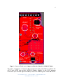
OP PM15-E Radiio Moduular Ceertificattion Instrucctions to OEM M Inteegratorrs V Version: 1.00.1 Daate: Apr 10, 2012 Email: [email protected] W http://w Web: www.omeshnnet.com/om mesh/ 2 Contents 1.0 Introduction ............................................................................................................................... 3 2.0 Allowed Antennas to be used with the Radio Module ............................................................. 3 3.0 RF Antenna Connection ............................................................................................................ 4 Figure 1 – Typical Application of OPM15-E Radio Module .................................................... 4 Figure 2 – Layer 1 (Top Layer) of Approved Interface Board for OPM15-E Radio ............. 6 4.0 Design and Production Test Procedures ................................................................................... 7 5.0 Required Host System Labeling ............................................................................................... 7 6.0 Required User Manual Statements............................................................................................ 8 Federal Communication Commission Sec 15.105 Interference Statement.............................. 8 FCC Sec 15.21 Caution ................................................................................................................. 8 FCC Sec 15.19 Labeling Statement ............................................................................................. 8 Industry Canada Statement ......................................................................................................... 8 Additional Warning Statement.................................................................................................... 9 www.omeshnet.com · t. 1-416-837-8980 · e. [email protected] OMESH Networks Inc. © 2012 3 1.0Introduction This document describes mandatory steps required by the OEM integrator when designing and manufacturing any system utilizing an OMESH Networks OPM15-E Radio Module (Part#: OPM15-E1, OPM15-E0; FCC ID: A3Q-OPM15E1; IC: 10131A-OPM15E1) which will be referred as the “OPM15 integrating system”. Also refer to the “OPM15 Software API Guide”, and “OPM15-E Radio (Low Power Version) Hardware Datasheet” available from OMESH Networks website and from your OMESH Networks customer support contact person. This document lists the mandatory responsibilities and actions of the OEM integrator. Failure to comply with all requirements and conditions in this document may result in non-compliance of “OPM15 integrating system” with FCC/IC rules and invalidate the OMESH Networks FCC/IC certification for the OPM15-E Radio Modules. 2.0AllowedAntennastobeusedwiththeRadioModule The OPM15-E Radio Module has two antenna pins and shall be connected to two antennas. Two categories of antennas have been certified with the OPM15-E Module: Category Reference Part# Dipole Antenna Alfa Networks Part#: ARS-N19 Ceramic Chip Pulse Antenna Part#: W3008C Antenna Maximal Gain 9dBi 2.2dBi In choosing an antenna category, the same category shall be used for both ANT1 and ANT2. You must contact OMESH Networks Regulatory Department to discuss necessary actions where alternate antenna categories are desired by the end integrator. Any such deviations from the certified antenna specification including maximal antenna gain must not be implemented without prior written acceptance. Unauthorized deviations may invalidate the FCC/IC certification of the OPM15-E Module. www.omeshnet.com · t. 1-416-837-8980 · e. [email protected] OMESH Networks Inc. © 2012 4 3.0RF FAntenna aConnecction Fiigure 1 – Typical App plication of OPM15-E Radio Mod dule The R RF antennaa connecttion pins ANT1 annd ANT2 are very critical inn layout design. The PCB line muust be designed to provide 50Ω nom minal charaacteristic m loss up to t radiatinng elementt. impedaance at 2.44GHz freqquency andd minimum www.omesshnet.com · t. 1-416-837-89880 · e. [email protected] m OMESH H Networks Innc. © 2012 5 The transmission line up to the antenna pads or the antenna connectors may be a micro strip or a stripline. In any case must be designed to achieve 50Ω characteristic impedance. Microstrip lines are usually easier to implement and the reduced number of layer transitions up to antenna connector simplifies the design and diminishes reflection losses. However, the electromagnetic field extends to the free air interface above the stripline and may interact with other circuitry. Buried striplines exhibit better shielding to external and internally generated interferences. They are therefore preferred for sensitive application. In case a stripline is implemented, carefully check that the via pad-stack does not couple with other signals on the crossed and adjacent layers. Minimize the transmission line length; the insertion loss should be minimized as much as possible. The transmission line should not have abrupt change to thickness and spacing to GND, but must be uniform and routed as smoothly as possible. The transmission line must be routed in a section of the PCB where minimal interference from noise sources can be expected. Route RF transmission line far from other sensitive circuits as it is a source of electromagnetic interference. Avoid coupling with VDD routing. Ensure solid metal connection of the adjacent metal layer on the PCB stack-up to main ground layer. Add GND vias around transmission line. Ensure no other signals are routed parallel to transmission line, or that other signals cross on adjacent metal layer. If the distance between the transmission line and the adjacent GND area (on the same layer) does not exceed 5 times the track width of the micro strip, use the “Coplanar Waveguide” model for 50 Ω characteristic impedance calculation. Don’t route microstrip line below discrete component or other mechanics placed on top layer. When terminating transmission line on antenna pads or antenna connectors, it is very important to strictly follow the antenna or connector manufacturer’s recommended layout. GND layer under RF connectors and close to buried vias should be cut out in order to remove stray capacitance and thus keep the RF line 50 Ω. In most cases the large active pad of the integrated antenna or antenna connector needs to have a GND keep-out (i.e. clearance) at least on first inner layer to reduce parasitic capacitance to ground. Note that the layout recommendation is not always available from connector manufacturer: e.g. the classical SMA Pin-Through-Hole needs to have GND cleared on all the layers around the central pin up to annular pads of the four GND posts. Check 50 Ω impedance of ANT line. Ensure no coupling occurs with other noisy or sensitive signals The approved reference design for the OPM15-E Radio Module (used as the certification test jig) has a structure of two layers described in the following. www.omeshnet.com · t. 1-416-837-8980 · e. [email protected] OMESH Networks Inc. © 2012 6 Figgure 2 – Laayer 1 (Top Layer) of A Approved Interface I B Board for O OPM15-E R Radio The Laayer 1 (topp layer, seee Figure 2) 2 providees four miccro strip liines to connnect the ANT1 and ANT T2 pins oof the OP PM15-E R Radio Moodule to tthe U.FL antenna W3008C connecctors (for eexternal diipole antennnas) and to the anteenna pads of Pulse W www.omesshnet.com · t. 1-416-837-89880 · e. [email protected] m OMESH H Networks Innc. © 2012 7 ceramic chip antennas. The ANT1 and ANT2 pins of the OPM15-E Module have to be soldered on the designed pad which is connected to the antenna connector by a micro strip. The characteristics of the micro strip line (coplanar wave guide) are the following: Width = 34 mils Maximal Length = 1534 mils (from ANT2 to the top W3008C pad) Gap (signal to GND) = 6 mils Thickness = 1.37 mils The Layer 2 (bottom layer) is a GND plane for the micro strip lines. Layer 2 thickness is 1.37 mils. Between the Layer 1 and Layer 2 is the dielectric (FR4), and the PCB thickness is 62 mils. 4.0DesignandProductionTestProcedures The design test procedure of the transmission lines can include direct measurement of the impedance at the two ends by using a network analyzer; in the mass production of any host devices, impedance control of the host’s printed circuit board can be used for production testing and controlling. 5.0RequiredHostSystemLabeling FCC ID and Industry Canada ID on Host System The Integrator must affix the module’s FCC ID and Industry Canada ID on the product, if the OMESH OPM15-E radio is installed inside the host system and its FCC ID and Industry Canada ID may not be visible. The FCC ID and Industry Canada ID label must appear on the outside of the host system visible to the user. Example wording to appear somewhere on the outside of the host system visible to the end user: Contains “FCC ID: A3Q-OPM15E1” & “IC: 10131A-OPM15E1” OR OPM15 Inside, FCC ID: A3Q-OPM15E1, IC: 10131A-OPM15E1 www.omeshnet.com · t. 1-416-837-8980 · e. [email protected] OMESH Networks Inc. © 2012 8 6.0RequiredUserManualStatements The FCC/IC requires the following text (or equivalent) included in the user documentation provided to the Integrators and End users: Federal Communication Commission Sec 15.105 Interference Statement This equipment has been tested and found to comply with the limits for a Class B digital device, pursuant to Part 15 of the FCC Rules. These limits are designed to provide reasonable protection against harmful interference in a residential installation. This equipment generates uses and can radiate radio frequency energy and, if not installed and used in accordance with the instructions, may cause harmful interference to radio communications. However, there is no guarantee that interference will not occur in a particular installation. If this equipment does cause harmful interference to radio or television reception, which can be determined by turning the equipment off and on, the user is encouraged to try to correct the interference by one of the following measures: - Reorient or relocate the receiving antenna. - Increase the separation between the equipment and receiver. - Connect the equipment into an outlet on a circuit different from that to which the receiver is connected. - Consult the dealer or an experienced radio/TV technician for help. FCC Sec 15.21 Caution Any changes or modifications not expressly approved by the OMESH Networks Inc. could void the user's authority to operate this equipment. FCC Sec 15.19 Labeling Statement This device complies with part 15 of the FCC Rules. Operation is subject to the following two conditions: (1) This device may not cause harmful interference, and (2) this device must accept any interference received, including interference that may cause undesired operation. Industry Canada Statement This device complies with Industry Canada licence-exempt RSS standard(s). Operation is subject to the following two conditions: (1) this device may not cause interference, and (2) this device must accept any interference, including interference that may cause undesired operation of the device. Le présent appareil est conforme aux CNR d'Industrie Canada applicables aux appareils radio exempts de licence. L'exploitation est autorisée aux deux conditions suivantes : (1) l'appareil ne doit pas produire de brouillage, et (2) l'utilisateur de l'appareil doit accepter tout brouillage radioélectrique subi, même si le brouillage est susceptible d'en compromettre le fonctionnement. www.omeshnet.com · t. 1-416-837-8980 · e. [email protected] OMESH Networks Inc. © 2012 9 RSS-Gen Notices for Transmitter Antenna Under Industry Canada regulations, this radio transmitter may only operate using an antenna of a type and maximum (or lesser) gain approved for the transmitter by Industry Canada. To reduce potential radio interference to other users, the antenna type and its gain should be so chosen that the equivalent isotropically radiated power (e.i.r.p.) is not more than that necessary for successful communication. This radio transmitter (IC:10131A-OPM15E1) has been approved by Industry Canada to operate with the antenna types listed in this document with the maximum permissible gain and required antenna impedance for each antenna type indicated. Antenna types not included in this document, having a gain greater than the maximum gain indicated for that type, are strictly prohibited for use with this device. Conformément à la réglementation d'Industrie Canada, le présent émetteur radio peut fonctionner avec une antenne d'un type et d'un gain maximal (ou inférieur) approuvé pour l'émetteur par Industrie Canada. Dans le but de réduire les risques de brouillage radioélectrique à l'intention des autres utilisateurs, il faut choisir le type d'antenne et son gain de sorte que la puissance isotrope rayonnée équivalente (p.i.r.e.) ne dépasse pas l'intensité nécessaire à l'établissement d'une communication satisfaisante. Le présent émetteur radio (IC:10131A-OPM15E1) a été approuvé par Industrie Canada pour fonctionner avec les types d'antenne énumérés ci-dessous et ayant un gain admissible maximal et l'impédance requise pour chaque type d'antenne. Les types d'antenne non inclus dans cette liste, ou dont le gain est supérieur au gain maximal indiqué, sont strictement interdits pour l'exploitation de l'émetteur. Additional Warning Statement SAR exclusion can be applied to a portable host and can be considered as a stand-alone unit, if the host consists of this module and no other radio inside. If there shall be another transmitter inside the host, the condition of simultaneous transmission and SAR evaluation may be needed as dependent on the position of the antennas and the distance between antennas. Amplifiers and active drivers are not permitted in host antenna circuits, as show in the approved reference design. The minimum spacing between the antenna traces of ANT1 and ANT2 can be 1 cm; and the spacing between the antenna components of ANT1 and ANT2 can be about 4 cm, as shown in the approved reference design. Antenna traces in the approved reference design use a two-layer FR4 PCB board. www.omeshnet.com · t. 1-416-837-8980 · e. [email protected] OMESH Networks Inc. © 2012 10 IMPORTANCE NOTICE The information in this document has been carefully reviewed and is believed to be accurate. Nonetheless, this document is subject to change without notice, and OMESH Networks Inc. (OMESH) assumes no responsibility for any inaccuracies that may be contained in the document, and makes no commitment to update or keep current the contained information, or to notify a person or organization of any updates. OMESH Networks reserves the right to make changes, at any time, in order to improve reliability, function or design and to attempt to supply the best product possible. OMESH Networks does not represent that products described herein are free from patent infringement or from any other third party right. OMESH NETWORKS MAKES NO WARRANTIES OF ANY KIND WITH REGARD TO THE CONTENT OF THIS DOCUMENT. IN NO EVENT SHALL OMESH NETWORKS BE LIABLE FOR DIRECT INDIRECT, SPECIAL, INCIDENTIAL SPECULATORY OR CONSEQUENTIAL DAMAGES ARISING FROM THE USE OR INABILITY TO USE THIS PRODUCT OR DOCUMENTATION, EVEN IF ADVISED OF THE POSSIBILITY OR SUCH DAMAGES. IN PARTICULAR, OMESH NETWORKS SHALL NOT HAVE LIABILITY FOR ANY HARDWARE, SOFTWARE, OR DATA TRANSMITTED OR OTHERWISE USED WITH THE PRODUCT, INCLUDING THE COSTS OF REPAIRING, REPLACING, INTEGRATING, INSTALLING OR RECOVERING SUCH HARDWARE, SOFTWARE OR DATA. OMESH NETWORKS SPECIFICALLY DISCLAIMS THE IMPLIED WARRANTIES OF MERCHANTIBILITY AND FITNESS FOR A PARTICULAR PURPOSE AS THEY MIGHT OTHERWISE APPLY TO THIS DOCUMENT AND TO THE IDEAS, MATERIAL AND INFORMATION EXPRESSED HEREIN. www.omeshnet.com · t. 1-416-837-8980 · e. [email protected] OMESH Networks Inc. © 2012


![Stealth Protect Series catalogue 2011_We[...]](http://vs1.manualzilla.com/store/data/005809212_1-caf297493bfcf938dba2b64bb0d79842-150x150.png)