1
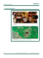
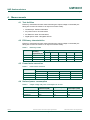
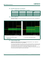
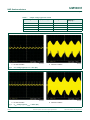
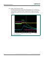
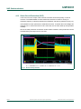
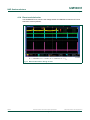
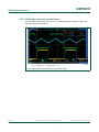
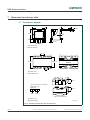
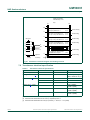
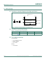
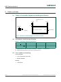
UM10831 TEA1716DB1258 demo board for 150 W all-in-one PC adapter Rev. 1 — 5 February 2015 User manual Document information Info Content Keywords TEA1716DB1258, TEA1716T, TEA1795T, all-in-one PC adapter, GreenChip SR, synchronous rectification, LLC, resonant, half-bridge, Power Factor Correction (PFC), controller, converter, burst mode, power supply, demo board Abstract This user manual describes the application of the TEA1716DB1258 demo board. The TEA1716T includes a Power Factor Correction (PFC) controller and a controller for a Half-Bridge resonant Converter (HBC). This user manual describes a 150 W resonant Switching Mode Power Supply (SMPS) for a typical all-in-one PC adapter design based on the TEA1716T and TEA1795T. The board provides an output of 19.5 V/7.7 A. It operates in normal mode for medium and high-power levels and in burst mode for low-power levels. Burst mode operation provides a reduction of power losses to increase performance. To increase the efficiency at high output power, the supply includes synchronous rectification by the TEA1795. The efficiency at high power is well above 90 %. The no-load power consumption is well below 500 mW. At 250 mW output power, the input power is below 500 mW (EUP lot6 compliant). UM10831 NXP Semiconductors TEA1716DB1258 demo board for 150 W all-in-one PC adapter Revision history Rev Date Description v.1 20150205 first issue Contact information For more information, please visit: http://www.nxp.com For sales office addresses, please send an email to: [email protected] UM10831 User manual All information provided in this document is subject to legal disclaimers. Rev. 1 — 5 February 2015 © NXP Semiconductors N.V. 2015. All rights reserved. 2 of 31 UM10831 NXP Semiconductors TEA1716DB1258 demo board for 150 W all-in-one PC adapter 1. Introduction WARNING Lethal voltage and fire ignition hazard The non-insulated high voltages that are present when operating this product, constitute a risk of electric shock, personal injury, death and/or ignition of fire. This product is intended for evaluation purposes only. It shall be operated in a designated test area by personnel qualified according to local requirements and labor laws to work with non-insulated mains voltages and high-voltage circuits. This product shall never be operated unattended. 1.1 Scope of this document This document describes the 150 W all-in-one PC adapter demo board using the TEA1716T and TEA1795T. A functional description is provided, supported by a set of measurements to show the all-in-one PC adapter characteristics. 1.2 TEA1716T The TEA1716T integrates a controller for PFC and a controller for an HBC. It provides the drive function for the discrete MOSFET of the upconverter and for the two discrete power MOSFETs in a resonant half-bridge configuration. The resonant controller part is a high-voltage controller for a Zero Voltage Switching (ZVS) LLC resonant converter. It includes a high-voltage level shift circuit and several protection features such as OverCurrent Protection (OCP), Open-Loop Protection (OLP), Capacitive Mode Protection (CMP), and a general purpose latched protection input. In addition to the resonant controller, the TEA1716T contains a PFC controller. The efficient operation of the PFC is obtained by functions such as quasi-resonant operation at high-power levels and quasi-resonant operation with valley skipping at lower power levels. OCP, OverVoltage Protection (OVP), and demagnetization sensing ensure safe operation under all conditions. The proprietary high-voltage Bipolar CMOS DMOS (BCD) power logic process makes direct start-up from the rectified universal mains voltage in an efficient way possible. A second low-voltage Silicon-On-Insulator (SOI) IC is used for accurate, high-speed protection functions and control. The combination of PFC and a resonant controller in one IC makes the TEA1716T suitable for all-in-one PC adapters. UM10831 User manual All information provided in this document is subject to legal disclaimers. Rev. 1 — 5 February 2015 © NXP Semiconductors N.V. 2015. All rights reserved. 3 of 31 UM10831 NXP Semiconductors TEA1716DB1258 demo board for 150 W all-in-one PC adapter &2033)& 616%2267 6160$,16 5&3527 616$8;3)& 66+%&(1 616&853)& 616)% 616287 616%8567 683,& *$7(3)& 3*1' 616&85+%& 6835(* QF *$7(/6 +% &)0,1 ,& 6*1' QF 683+6 683+9 *$7(+6 DDD Fig 1. TEA1716T pin configuration 1.3 TEA1795T The TEA1795T GreenChip SR is a synchronous rectification control IC that does not require any external components to tune the timing. Used in all-in-one PC adapter designs, the GreenChip SR offers a wide VCC operating range between 8.5 V and 38 V, minimizing the number of external components required and enabling simpler designs. In addition, the high driver output voltage (10 V) makes the GreenChip SR compatible with all MOSFET brands. 66$ *1' 66% 9&& 7($7 *'$ *'% '6$ '6% DDD Fig 2. TEA1795T pinning configuration 1.4 Setup of the 150 W all-in-one PC adapter The board can operate at a mains input voltage of between 90 V and 264 V (universal mains). The demo board contains two subcircuits: • A PFC of BCM-type • An HBC of resonant LLC-type The TEA1716T controls both converters. At low-power levels, the converters operate in burst mode to reduce power losses. The TEA1795T controls the synchronous rectification stage in the LLC converter. UM10831 User manual All information provided in this document is subject to legal disclaimers. Rev. 1 — 5 February 2015 © NXP Semiconductors N.V. 2015. All rights reserved. 4 of 31 UM10831 NXP Semiconductors TEA1716DB1258 demo board for 150 W all-in-one PC adapter The purpose of the TEA1716DB1258 demo board is to demonstrate the operation of the TEA1716T and TEA1795T in a single output supply including burst mode operation. The performance is according to current general standards including the EuPlot6 requirements. It can be used as a starting point for further development. 1.5 Input and output properties Table 1. TEA1716DB1258 input data Symbol Parameter Conditions Specification Vi input voltage AC 90 V to 264 V (RMS) fi input frequency Pi(noload) no-load input power at 230 V/50 Hz < 200 mW Pi(load=250mW) standby power consumption at 230 V/50 Hz < 500 mW Conditions Specification Table 2. 47 Hz to 60 Hz TEA1716DB1258 output data Symbol Parameter Vo output voltage Vo(ripple)(p-p) peak-to-peak output ripple voltage 20 MHz bandwidth < 300 mV 19.5 V Io output current continuous 0 A to 7.65 A 2. Safety warning The board must be connected to the mains voltage. Avoid touching the board during operation at all times. An isolated housing is obligatory when used in uncontrolled, non-laboratory environments. Galvanic isolation of the mains phase using a variable transformer is always recommended. Figure 3 shows the symbols on how to recognize these devices. 019aab174 019aab173 a. Isolated Fig 3. UM10831 User manual b. Not isolated Isolation symbols All information provided in this document is subject to legal disclaimers. Rev. 1 — 5 February 2015 © NXP Semiconductors N.V. 2015. All rights reserved. 5 of 31 UM10831 NXP Semiconductors TEA1716DB1258 demo board for 150 W all-in-one PC adapter 3. Board photographs a. Top view b. Bottom view Fig 4. UM10831 User manual TEA1716DB1258 demo board 150 W all-in-one PC adapter All information provided in this document is subject to legal disclaimers. Rev. 1 — 5 February 2015 © NXP Semiconductors N.V. 2015. All rights reserved. 6 of 31 UM10831 NXP Semiconductors TEA1716DB1258 demo board for 150 W all-in-one PC adapter 4. Measurements 4.1 Test facilities Efficiency measurements were made measuring the output voltage on the board (not taking into account the losses in an output connection cable). • • • • Oscilloscope: Tektronix DPO3034 AC power source: Chroma 61603 DC Electronic load: Chroma 63010 Digital power meter: Yokogawa WT210 4.2 Efficiency characteristics Efficiency measurements were made measuring the output voltage on the board (not taking into account the losses in an output connection cable). Table 3. Efficiency results Condition Energy Star 2.0 Efficiency (%) efficiency Average 25 % load requirement (%) 50 % load 75 % load 100 % load 100 V/60 Hz > 87 91.8 89.9 92.2 92.9 92.1 115 V/60 Hz > 87 92.1 89.9 92.5 93.3 92.7 230 V/50 Hz > 87 93.2 90.3 93.9 94.4 94.1 4.3 Power factor correction Table 4. Power factor correction Condition Power factor 100 V/60 Hz 25 % load 50 % load 75 % load 100 % load 0.95 0.98 0.99 0.99 115 V/60 Hz 0.95 0.97 0.99 0.99 230 V/50 Hz 0.79 0.88 0.92 0.95 4.4 No-load power consumption Table 5. UM10831 User manual Output voltage and power consumption at no-load Condition Energy Star 2.0 requirement (mW) Output voltage (V) No-load power consumption (mW) 100 V/60 Hz 500 19.6 140 115 V/60 Hz 500 19.6 140 230 V/50 Hz 500 19.6 180 All information provided in this document is subject to legal disclaimers. Rev. 1 — 5 February 2015 © NXP Semiconductors N.V. 2015. All rights reserved. 7 of 31 UM10831 NXP Semiconductors TEA1716DB1258 demo board for 150 W all-in-one PC adapter 4.5 Standby load power consumption Table 6. Standby output voltage and power consumption Condition Output power (mW) Output voltage (V) Power consumption (mW) 100 V/60 Hz 250 19.6 430 115 V/60 Hz 250 19.6 430 230 V/50 Hz 250 19.6 450 4.6 Start-up behavior The start-up time during full load is depending on input mains AC levels. The duration is less than 1 second. Ch. 1: Vout; Ch. 4: AC input a. Input: 90 V (AC) full load condition Fig 5. b. Input: 264 V (AC) full load condition Start-up time 4.7 Output voltage ripple Ripple and noise are measured at full output load, buffered with a 10 F capacitor in parallel with a high-frequency 0.1 F capacitor. The varying input voltage of the resonant converter causes a frequency component in the output ripple voltage that is related to the mains voltage frequency, either 50 Hz or 60 Hz. The high-frequency component of the output ripple voltage is the result of the high-frequency switching frequency current ripple transferred from the primary side to the secondary side output capacitors and the output load. UM10831 User manual All information provided in this document is subject to legal disclaimers. Rev. 1 — 5 February 2015 © NXP Semiconductors N.V. 2015. All rights reserved. 8 of 31 UM10831 NXP Semiconductors TEA1716DB1258 demo board for 150 W all-in-one PC adapter Table 7. Output voltage ripple test results Mains voltage Output power (W) 150 continue mode 53 90 V/60 Hz no-load burst mode 112 264 V/50 Hz 150 continue mode 63 264 V/50 Hz no-load burst mode 112 b. Full load condition Vout voltage ripple (Vmains = 90 V (AC) a. No-load condition Fig 7. Voltage ripple (mV/p-p) 90 V/60 Hz a. No-load condition Fig 6. Switching condition b. Full load condition Vout voltage ripple (Vmains = 264 V (AC) UM10831 User manual All information provided in this document is subject to legal disclaimers. Rev. 1 — 5 February 2015 © NXP Semiconductors N.V. 2015. All rights reserved. 9 of 31 UM10831 NXP Semiconductors TEA1716DB1258 demo board for 150 W all-in-one PC adapter 4.8 Dynamic response behavior Output voltage function dynamic load test: 0.05 A; 90 % load; 0.12 s; f = 100 Hz Ch. 1 = Vout; Ch. 4 = Iout a. 90 V (AC); 1 kHz Fig 8. b. 90 V (AC); 100 Hz Load step behavior UM10831 User manual All information provided in this document is subject to legal disclaimers. Rev. 1 — 5 February 2015 © NXP Semiconductors N.V. 2015. All rights reserved. 10 of 31 UM10831 NXP Semiconductors TEA1716DB1258 demo board for 150 W all-in-one PC adapter 4.9 Hold-up time The output is set to full load and the mains supply voltage of 100 V is disconnected. The time that passes before the output voltage drops to below 90 % of its initial value is then measured. The hold-up time is 26 ms. Ch. 2 = Vout; Ch. 4 = Input AC voltage Fig 9. UM10831 User manual Hold-up time All information provided in this document is subject to legal disclaimers. Rev. 1 — 5 February 2015 © NXP Semiconductors N.V. 2015. All rights reserved. 11 of 31 UM10831 NXP Semiconductors TEA1716DB1258 demo board for 150 W all-in-one PC adapter 4.10 OverPower Protection (OPP) The OPP is activated when the current exceeds 9.5 A (195 W). It corresponds with a load condition that is 23 % higher than the rated power for continuous use. The SNSCURHBC function of the TEA1716 detects OPP. This function monitors the primary resonant current. When the voltage on the SNSCURHBC pin exceeds 0.5 V, the RCPROT protection timer is started. The RCPROT function performs its restart timer function. It restarts when the voltage has dropped to 0.5 V. When the OPP is removed, the converter starts up and operates normally. Ch. 1 = SNSCURHBC; Ch. 2 = RCPROT; Ch. 3 = Vout; Ch. 4 = Iout Fig 10. Overpower protection UM10831 User manual All information provided in this document is subject to legal disclaimers. Rev. 1 — 5 February 2015 © NXP Semiconductors N.V. 2015. All rights reserved. 12 of 31 UM10831 NXP Semiconductors TEA1716DB1258 demo board for 150 W all-in-one PC adapter 4.11 OverVoltage Protection (OVP) The worst-case overvoltage happens during no-load. When the output voltage becomes too high (overvoltage event), the SNSOUT pin is triggered to exceed 3.5 V and latch IC operation. Even when the overvoltage event is removed, no restart occurs because the protection is a latched protection. However, if a latch reset is implemented, a restart does occur. Ch. 1 = SNSOUT; Ch. 2 = RCPROT; Ch. 3 = Vout; Ch. 4 = SNSFB Fig 11. Overvoltage protection UM10831 User manual All information provided in this document is subject to legal disclaimers. Rev. 1 — 5 February 2015 © NXP Semiconductors N.V. 2015. All rights reserved. 13 of 31 UM10831 NXP Semiconductors TEA1716DB1258 demo board for 150 W all-in-one PC adapter 4.12 Open-Loop Protection (OLP) The SNSFB function detects an open output voltage feedback loop. It is triggered over 8.2 V until the protection timer RCPROT reaches its protection level (4 V). The RCPROT function performs a restart timer function. It restarts when the voltage has dropped to 0.5 V. When the feedback open-loop is removed, the converter starts up and operates normally. Ch. 1 = SNSOUT; Ch. 2 = RCPROT; Ch. 3 = Vout; Ch. 4 = SNSFB Fig 12. Open-loop protection UM10831 User manual All information provided in this document is subject to legal disclaimers. Rev. 1 — 5 February 2015 © NXP Semiconductors N.V. 2015. All rights reserved. 14 of 31 UM10831 NXP Semiconductors TEA1716DB1258 demo board for 150 W all-in-one PC adapter 4.13 Short Circuit Protection (SCP) A short circuit on the output of the resonant converter causes the primary current to increase. The SNSCURHBC function detects this increase. It leads to running on maximum frequency until the protection timer RCPROT reaches its protection level (4 V). The RCPROT function performs its restart timer function. It restarts when the voltage has dropped to 0.5 V. When the short circuit is removed, the converter starts up and operates normally. SCP is the main protection mechanism. Under certain conditions, other protections can be activated during the output short circuit test. Ch. 1 = SNSBURST; Ch. 2 = GATELS; Ch. 3 = GATEPFC; Ch. 4 = Vout Fig 13. Short circuit protection UM10831 User manual All information provided in this document is subject to legal disclaimers. Rev. 1 — 5 February 2015 © NXP Semiconductors N.V. 2015. All rights reserved. 15 of 31 UM10831 NXP Semiconductors TEA1716DB1258 demo board for 150 W all-in-one PC adapter 4.14 Burst mode behavior The SNSBURST level, which is the voltage divider from SNSFB controls the PFC and HBC burst mode hysteresis. Ch. 1 = SNSBURST; Ch. 2 = GATELS; Ch. 3 = GATEPFC; Ch. 4 = Vout Fig 14. Burst mode behavior during no-load UM10831 User manual All information provided in this document is subject to legal disclaimers. Rev. 1 — 5 February 2015 © NXP Semiconductors N.V. 2015. All rights reserved. 16 of 31 UM10831 NXP Semiconductors TEA1716DB1258 demo board for 150 W all-in-one PC adapter 4.15 Half-bridge measurement waveforms The half-bridge node duty-cycle is 50 %. The CFMIN oscillator frequency is twice the half-bridge switching frequency. Ch. 1 = GATELS; Ch. 2 = CFMIN; Ch. 4 = HB Fig 15. Half-bridge measurements during nominal output UM10831 User manual All information provided in this document is subject to legal disclaimers. Rev. 1 — 5 February 2015 © NXP Semiconductors N.V. 2015. All rights reserved. 17 of 31 UM10831 NXP Semiconductors TEA1716DB1258 demo board for 150 W all-in-one PC adapter 4.16 Synchronous rectification The TEA1795T IC is used for synchronous rectification. It replaces the rectifier diodes at the secondary side of the resonant converter. Ch. 1 = Vgs-1; Ch. 2 = Vds-1; Ch. 3 = Vgs-2; Ch. 4: Vds-2 Fig 16. TEA1795T synchronous rectification waveforms during nominal output UM10831 User manual All information provided in this document is subject to legal disclaimers. Rev. 1 — 5 February 2015 © NXP Semiconductors N.V. 2015. All rights reserved. 18 of 31 xxxxxxxxxxxxxxxxxxxxx xxxxxxxxxxxxxxxxxxxxxxxxxx xxxxxxx x x x xxxxxxxxxxxxxxxxxxxxxxxxxxxxxx xxxxxxxxxxxxxxxxxxx xx xx xxxxx xxxxxxxxxxxxxxxxxxxxxxxxxxx xxxxxxxxxxxxxxxxxxx xxxxxx xxxxxxxxxxxxxxxxxxxxxxxxxxxxxxxxxxx xxxxxxxxxxxx x x xxxxxxxxxxxxxxxxxxxxx xxxxxxxxxxxxxxxxxxxxxxxxxxxxxx xxxxx xxxxxxxxxxxxxxxxxxxxxxxxxxxxxxxxxxxxxxxxxxxxxxxxxx xxxxxxxx xxxxxxxxxxxxxxxxxxxxxxxxx xxxxxxxxxxxxxxxxxxxx xxx NXP Semiconductors UM10831 User manual 5. Schematic ' 1 ) $ 9 / / 5 0ȍ %' *%8 / & ) 3* LQOHW & S) 9 5 0ȍ 1 ' %<9; / 34+ / 6* 3* %& 5 & ) 9 & ) 9 & QF 5 ' QF QF 62' 5 ȍ 5 Nȍ 4 30%7 3* 5 0ȍ & ) 9 & QF 5 0ȍ 5 ȍ : & Q) 9 5 Nȍ 5 QF 5 0ȍ 3* & Q) 9 5 Nȍ 6* 5 Nȍ 5 ȍ ,&3$57 *$7(3)& 616$8;3)& 5 6160$,16 Nȍ 3*1' & ) 9 & ) 9 6* Fig 17. TEA1716DB1258 schematic - part 1 7($ 3$57 62 616&853)& & QF 616%2267 683+9 6* 5 &2033)& Nȍ & Q) 9 3* 6* & Q) 9 DDD UM10831 19 of 31 © NXP Semiconductors N.V. 2015. All rights reserved. 5 Nȍ TEA1716DB1258 demo board for 150 W all-in-one PC adapter Rev. 1 — 5 February 2015 All information provided in this document is subject to legal disclaimers. & QF 5 0ȍ & S) 9 ȍ & S) 9 9EXONBFDS 4 5&3 72 xxxxxxxxxxxxxxxxxxxxx xxxxxxxxxxxxxxxxxxxxxxxxxx xxxxxxx x x x xxxxxxxxxxxxxxxxxxxxxxxxxxxxxx xxxxxxxxxxxxxxxxxxx xx xx xxxxx xxxxxxxxxxxxxxxxxxxxxxxxxxx xxxxxxxxxxxxxxxxxxx xxxxxx xxxxxxxxxxxxxxxxxxxxxxxxxxxxxxxxxxx xxxxxxxxxxxx x x xxxxxxxxxxxxxxxxxxxxx xxxxxxxxxxxxxxxxxxxxxxxxxxxxxx xxxxx xxxxxxxxxxxxxxxxxxxxxxxxxxxxxxxxxxxxxxxxxxxxxxxxxx xxxxxxxx xxxxxxxxxxxxxxxxxxxxxxxxx xxxxxxxxxxxxxxxxxxxx xxx NXP Semiconductors UM10831 User manual 9EXONBFDS ' 5 4 6. 72 QF QF 62' 5 5 QF ȍ / 5 Nȍ 7 5 4 6. 72 QF QF 62' 5 & S) & QF ȍ ' 4 3601536 72 & QF )/< ,& '6$ '6% Q) 9 *1'B($57+ Nȍ 62 *'% *1' 66% *1'B($57+ 9RXW =' 9 62' 9 62' 5 ȍ *$7(+6 616&85+%& & S)9 6* 5 ȍ 6* QF 6* 6*1' &)0,1 616%8567 616)% & Q) & QP 66+%&(1 & ) 9 5 ȍ 6* 3&3527 616%2267 7($7 62 6* 6* 5 6835(* 5 Nȍ 5 Nȍ & QF ) 627 9 5 Nȍ 6* =' 6* *1' 4 3601536 72 *1'B($57+ 5 Nȍ *1' 5 QF *$7(/6 6835(* & ) 9 683+9 & ) 9 3* *$7(3)& 3* Nȍ 5 QF 5 QF & QF ,& /79$ 3* 5 Nȍ ' (6% 60$ 5 Nȍ 5 Nȍ & ) 9 6* 3* 683,& 6* 6835(* & Q) 9 616&853)& 616$8;3)& Nȍ ' %$6+ 627 57 Nȍ 6* &2033)& 4 QF 627 & Q) : & QF QF 287 287 6* 5 Nȍ ,19 $3$ ,& *1' 5 Nȍ 1,19 1,19 ,19 9&& 4 %& 627 Nȍ 5 Nȍ 5 Nȍ *1'B($57+ & ) 9 5 6835(* & 5 ȍ 5 QF 5 ) 9 Nȍ 5 Nȍ & Q) *1'B($57+ *1'B($57+ ,& /79$ 4 QF 627 5 Nȍ & 5 616287 6160$,16 ' (6% 60$ & ) 9 & ) 9 3*1' QF 5 QF & ) 9 & 6* S) 5 Nȍ 5 Nȍ 6* 6* *1'B($57+ *1' 6* DDD Fig 18. TEA1716DB1258 schematic - part 2 (HBC stage) UM10831 20 of 31 © NXP Semiconductors N.V. 2015. All rights reserved. 5 ȍ & QF 5 ȍ : & S) Q) 9 6* 683+6 ' %$9 627 ,& )9 +% 5 ȍ S) N9 & ) 9 TEA1716DB1258 demo board for 150 W all-in-one PC adapter Rev. 1 — 5 February 2015 All information provided in this document is subject to legal disclaimers. ' (660$ & ȍ & 6835(* & & ) 9 5 Nȍ 3* 5 & ) 9 =' 5 ȍ 5 Nȍ & S) 5 0ȍ : & ) 9 7($ & S) 66$ 9 && *'$ *1'B($57+ & 5 5 QF 5 ȍ 5 0ȍ : UM10831 NXP Semiconductors TEA1716DB1258 demo board for 150 W all-in-one PC adapter 6. Bill Of Materials (BOM) Table 8. TEA1716DB1258 bill of materials Reference Description and values BC101 bead core; axial lead; Wide Band RH-type (WBRH); 3.5 mm 4.7 mm 0.8 mm; 3L - BD101 diode; bridge diode; 4 A; 800 V GBU408 Lite-On C101; C102 capacitor; ceramic; Y1-capacitor; 220 pF; 250 V (AC) - Murata C103 capacitor; X-capacitor; 0.47 F; 275 V (AC); MKP/HJC - - C104 capacitor; 680 nF; 450 V (DC); radial lead; MPPN/HJC - - C105 capacitor; 1 F; 450 V (DC); radial lead; MPPN/HJC - - C106 capacitor; 100 pF; 630 V (DC); 1206; SMD; NPO; MLCC - - C107 capacitor; 4.7 nF; 25 V (DC); 0603; SMD; X7R; MLCC - C108; C108-1 capacitor; 2.2 F; 16 V (DC); 1206; SMD; X7R; MLCC - C109 capacitor; 47 nF; 25 V; 0603; SMD; X7R; MLCC - - C110 capacitor; electrolytic; 180 F; 420 V (DC); 30 mm 25 mm (width height); KMQ; NCC - - C111 capacitor; 150 nF; 25 V; 0603; SMD; X7R; MLCC - C112 capacitor; 470 nF; 25 V; 0603; SMD; X7R; MLCC - C200 capacitor; 22 nF; 600 V; radial lead; MP3/HJC - - C203 capacitor; 220 F; 50 V; 105 C; 10 mm 16 mm; E/C; radial lead; KY/NCC - - C204 capacitor; 10 F; 50 V; 105 C; 5 mm 11 mm; E/C; radial lead; KY/NCC - C205; C304 capacitor; 100 nF; 50 V; 0603; SMD; X7R; MLCC - C206; C212 capacitor; 2.2 nF; 25 V; 1206; SMD; X7R; MLCC - C207; C313 capacitor; 1 nF; 25 V; 0603; SMD; X7R; MLCC - - C210 capacitor; 10 nF; 25 V; 1206; SMD; X7R; MLCC - - C211 capacitor; 470 pF; 1 kV; 1206; SMD; NPO; MLCC - - UM10831 User manual Part number All information provided in this document is subject to legal disclaimers. Rev. 1 — 5 February 2015 Manufacturer © NXP Semiconductors N.V. 2015. All rights reserved. 21 of 31 UM10831 NXP Semiconductors TEA1716DB1258 demo board for 150 W all-in-one PC adapter Table 8. TEA1716DB1258 bill of materials …continued Reference Description and values C214 capacitor; 330 nF; 25 V; 0805; SMD; X7R; MLCC - C215 capacitor; 270 pF; 25 V; 0603; SMD; X7R; MLCC - C216 capacitor; 100 nF; 25 V; 0805; SMD; X7R; MLCC - C217 capacitor; 2.2 F; 25 V; 0805; SMD; X7R; MLCC - C219; C309; C310 capacitor; 100 nF; 25 V; 0603; SMD; X7R; MLCC - C222 - - C305; C306; C307 capacitor; electrolytic; 820 F; 25 V; KZH: 10 mm 20 mm (width height); NCC - C311 capacitor; 47 nF; 25 V; 0603; SMD; X7R; MLCC - - C315; C316 capacitor; 22 pF; 50 V; 0603; SMD; X7R; MLCC - - C321; C322 capacitor; 100 pF; 50 V; 0603; SMD; X7R; MLCC - C401 capacitor; ceramic; Y1-capacitor; 680 pF; 250 V (AC) - Murata D101 diode; general purpose; 3 A; 1 kV; 1N5408 - - D102 diode; ultrafast power diode BYV29X-600 NXP Semiconductors D203; D204 diode; ultrafast rectifier; 100 V; 1 A; SMA ES1B - D206 diode; ultrafast rectifier; 600 V; 1 A; SMA ES1J - D208 diode; high-speed switching diode; 100 V; BAS16H SOD123F - D209 diode; high-speed double diode; 75 V; SOT23 BAV99 - ZD321; ZD322 Zener diode; 30 V; SOD323 ZBX84J-B30V - F101 fuse; 3.15 A; 250 V; MST(conquer) - - IC101 IC; TEA1716T resonant power supply control IC with PFC SO24 NXP Semiconductors IC301 IC; TEA1795T GreenChip synchronous rectifier controller SO8 NXP Semiconductors IC303 IC; AP4310A dual OP amplifier and voltage reference; BCD SO8 - IC304; IC305 high-density mounting type photocoupler; LTV817A DIP 4 Lite-On inlet AC Inlet 3P - - L101 choke; EMI; 7.35 mH; SA382/HJC - L102 choke; EMI; 11.07 mH SA383/HJC - L103 choke; filter; 170 H SA384/HJC - L104 choke; PFC; 315 H; PQ2625 SA136/HJC - UM10831 User manual Part number capacitor; 10 nF; 25 V; 0603; SMD; X7R; MLCC All information provided in this document is subject to legal disclaimers. Rev. 1 — 5 February 2015 Manufacturer © NXP Semiconductors N.V. 2015. All rights reserved. 22 of 31 UM10831 NXP Semiconductors TEA1716DB1258 demo board for 150 W all-in-one PC adapter Table 8. TEA1716DB1258 bill of materials …continued Reference Description and values Part number Manufacturer L201 choke; 44 H; ATQ2116.8 SA135/HJC - T1 transformer; 800 H; PQ3221 SA137/HJC - Q101 MOSFET; 600 V; 16 A; TO220 IPA60R199CP Infineon Q102; Q203 transistor; switching; PNP; SOT23 PMBT4403 NXP Semiconductors Q201; Q202 MOSFET; 600 V; 10 A; TO220 2SK3569 Toshiba Q301; Q302 MOSFET; 60 V; 92 A; TO220AB PSMN7R6-60PS NXP Semiconductors R101; R102 resistor; thin film chip; 1.5 M; 5 %; 1206; SMD - R103 resistor; thin film chip; 523 k; 1 %; 1206; SMD - R104 resistor; thin film chip; 40.2 k; 1 %; 0603; SMD - - R105 resistor; thin film chip; 5.1 k; 1 %; 0603; SMD - R107; R201; R204 resistor; thin film chip; 10 ; 5 %; 0805; SMD - - R109 resistor; thin film chip; 2.2 ; 5 %; 0805; SMD - - R110 resistor; thin film chip; 0.05 W; 1 %; 2 W; 2512; SMD - Taiwan Semiconductor R111; R112; R113 resistor; thin film chip; 3.3 M; 1 %; 1206; SMD - R114 resistor; thin film chip; 64.9 k; 1 %; 0603; SMD - - R114-1 resistor; thin film chip; 3 M; 1 %; 0603; SMD - - R115; RJ1; RJ2; resistor; thin film chip; 0 ; 5 %; 1206; RJ3; RJ4; RJ5; SMD RJ6; RJ7; RJ8; RJ9; RJ10; RJ11; RJ12; RJ13; RJ14; RJ15; R228 - - R116; R231 resistor; thin film chip; 18.2 k; 1 %; 0603; SMD - - R117; R217 resistor; thin film chip; 12 k; 1 %; 0603; SMD - - R118 resistor; thin film chip; 33 k; 5 %; 0603; SMD - - R208 resistor; thin film chip; 332 k; 1 %; 0603; SMD - R209 resistor; thin film chip; 40.2 k; 1 %; 0603; SMD - - R210 resistor; thin film chip; 12.4 ; 1 %; 1206; SMD - R213 resistor; thin film chip; 10 ; 1 %; 1206; SMD - UM10831 User manual - All information provided in this document is subject to legal disclaimers. Rev. 1 — 5 February 2015 © NXP Semiconductors N.V. 2015. All rights reserved. 23 of 31 UM10831 NXP Semiconductors TEA1716DB1258 demo board for 150 W all-in-one PC adapter Table 8. TEA1716DB1258 bill of materials …continued Reference Description and values Part number Manufacturer - - R216 resistor; thin film chip; 150 k; 1 %; 0603; SMD - R218 resistor; thin film chip; 18.2 k; 1 %; 0603; SMD - - R220 resistor; thin film chip; 6.2 k; 1 %; 0603; SMD - R223 resistor; thin film chip; 2 k; 1 %; 0603; SMD - - R302; R305 resistor; thin film chip; 4.7 ; 5 %; 0805; SMD - - R303; R306 resistor; thin film chip; 1 k; 1 %; 0805; SMD - - R307 resistor; thin film chip; 12 m; 1 %; 2 W; 2512; SMD - Taiwan Semiconductor R308; R316; R321; resistor; thin film chip; 10 k; 1 %; 0603; R323 SMD - - R309 resistor; thin film chip; 30.9 k; 1 %; 0603; SMD - - R310 resistor; thin film chip; 4.53 k; 1 %; 0603; SMD - - R310-1 resistor; thin film chip; 294 k; 1 %; 0603; SMD - R311 resistor; thin film chip; 300 k; 1 %; 0603; SMD - R313 resistor; thin film chip; 191 ; 1 %; 0603; SMD - - R314 resistor; thin film chip; 2 k; 1 %; 0603; SMD - - R317 resistor; thin film chip; 51 k; 1 %; 0603; SMD - - R322; R324 resistor; 1.2 M; 5 %; 1/4 W; DIP - - RT201 thermistor; NTC; 100 k; 1 % TTC3A104F4192EY Thinking HS1 heat sink; for Q101, D102, Q201, Q202 - - R214; R215; R225 resistor; thin film chip; 0 ; 5 %; 0603; SMD HS2 heat sink; for BD101 - - HS3 heat sink; for Q301, Q302 - - UM10831 User manual All information provided in this document is subject to legal disclaimers. Rev. 1 — 5 February 2015 © NXP Semiconductors N.V. 2015. All rights reserved. 24 of 31 UM10831 NXP Semiconductors TEA1716DB1258 demo board for 150 W all-in-one PC adapter 7. Resonant transformer data 7.1 Transformer diagram PD[ PD[ PD[ WDSH FRUHDGGHSR[\ GLPHQVLRQVLQPP D6LGHDQGHQGYLHZV +-&6$' +-&[[[[ PD[ GLPHQVLRQVLQPP E%RWWRPDQGWRSYLHZV PLQ SLQFXWRIISLQFXWRII JDSFRUHRQWRS GDWHFRGH <($5 PLQ :((. \HOORZP\ODUWDSH DWSLQDQGERWWRPVLGH GLPHQVLRQVLQPP F0RXQWLQJLQVWUXFWLRQV DDD Fig 19. Resonant transformer data: HJC-SA137D UM10831 User manual All information provided in this document is subject to legal disclaimers. Rev. 1 — 5 February 2015 © NXP Semiconductors N.V. 2015. All rights reserved. 25 of 31 UM10831 NXP Semiconductors TEA1716DB1258 demo board for 150 W all-in-one PC adapter ZLQGLQJFRQVWUXFWLRQ LQVWUXFWLRQWDSHPLO WDSH SLQ WRS 7V 18(:[ 18(:[ 7V 7V VSDFHGZLQGLQJ 7 1)/<7(;(/= 7V 1)/<7(;(/= 7V FORVHGZLQGLQJ 1)/<7(;(/= 7V 1)/<7(;(/= 7V FORVHGZLQGLQJ 1)/<7(;(/= 7V 1)/<7(;(/= 7V FORVHGZLQGLQJ 7 WHIORQWXEH 7 1 111 1 7 )O\ 111 1 FORVHGZLQGLQJ 7 FRSSHUIRLO (FRSSHUIRLOPLO[PPZ OHDGZLUHGLDWRSLQ7V 1/LW] ( 7V FORVHGZLQGLQJ EREELQ SULPDU\ VHFRQGDU\ PDUJLQWDSHPP DDD Fig 20. Transformer schematic diagram and winding overview 7.2 Transformer electrical specification Table 9. Transformer electrical specifications Parameter Start Finish Specification inductance[1] 1 2 800 H; 3 % 1 1 secondary winding short; maximum 15 H 1 2 maximum 165 m 4 5 maximum 490 m leakage inductance[1] DC resistance[2] 12 fly1 maximum 6.10 m 5 2.58 V (RMS); 0.08 V (RMS) 12 fly1 0.975 V (RMS); 0.08 V (RMS) fly1 9 0.975 V (RMS); 0.08 V (RMS) voltage ratio[3]; input 1, 4 2 UM10831 User manual [1] Measured with HP: 4284A LCR meter (or equivalent); f = 100 kHz; V = 1 V (RMS) at 25 C. [2] Measured with CHEN HWA 502 AC meter (or equivalent) at 25 C. [3] Measured with CHEN HWA310 meter (or equivalent); f = 20 kHz; V = 10 V (RMS). All information provided in this document is subject to legal disclaimers. Rev. 1 — 5 February 2015 © NXP Semiconductors N.V. 2015. All rights reserved. 26 of 31 UM10831 NXP Semiconductors TEA1716DB1258 demo board for 150 W all-in-one PC adapter 8. PFC coil data 8.1 Transformer schematic diagram and winding specification ZLQGLQJFRQVWUXFWLRQ LQVWUXFWLRQWDSHPLO WDSH SLQVLGH WRSVLGH 7V WHIORQWXEH 18(:PP[ 1 7V VSDFHGZLQGLQJ 7V FORVHGZLQGLQJ 1 7 VHFRQGDU\ SULPDU\ 1/LW]PP[ EREELQ PDUJLQWDSHPP7V DDD Fig 21. Transformer schematic diagram and winding overview 8.2 Transformer electrical specification Table 10. Transformer electrical specifications Parameter Start Finish Specification inductance[1] 3 1 315 H; 3 % 3 1 not applicable leakage [1] inductance[1] Measured with HP: 4284A LCR meter (or equivalent); f = 100 kHz; V = 1 V (RMS) at 25 C. 8.3 Core, bobbin and marking Core and bobbin: • Core: PQ2625 (JPP-44A) • Bobbin: PM9820 • Ae: 120 mm2 Marking: • HJC-SA136A UM10831 User manual All information provided in this document is subject to legal disclaimers. Rev. 1 — 5 February 2015 © NXP Semiconductors N.V. 2015. All rights reserved. 27 of 31 UM10831 NXP Semiconductors TEA1716DB1258 demo board for 150 W all-in-one PC adapter 9. Choke coil data 9.1 Choke coil schematic diagram and winding specification ZLQGLQJFRQVWUXFWLRQ LQVWUXFWLRQWDSHPLO WDSH SLQVLGH WRSVLGH 7V WHIORQWXEH 1 1/LW]PP[ SULPDU\ 7V FORVHGZLQGLQJ VHFRQGDU\ EREELQ DDD Fig 22. Transformer schematic diagram and winding overview 9.2 Transformer electrical specification Table 11. Transformer electrical specifications Parameter Start Finish Specification inductance[1] 4 6 44 H; 3 % leakage inductance[1] 3 1 not applicable 4 6 maximum 145 m DC resistance[2] [1] Measured with HP: 4284A LCR meter (or equivalent); f = 100 kHz; V = 1 V (RMS) at 25 C. [2] Measured with CHEN HWA 502 AC meter (or equivalent) at 25 C. 9.3 Core, bobbin and marking Core and bobbin: • Core: ATQ21/16.8 (JPP-44A) • Bobbin: PM9820 Marking: • HJC-SA135 UM10831 User manual All information provided in this document is subject to legal disclaimers. Rev. 1 — 5 February 2015 © NXP Semiconductors N.V. 2015. All rights reserved. 28 of 31 UM10831 NXP Semiconductors TEA1716DB1258 demo board for 150 W all-in-one PC adapter 10. Abbreviations Table 12. UM10831 User manual Abbreviations Acronym Description BCD Bipolar CMOS DMOS OLP Open-Loop Protection OPP OverPower Protection OVP OverVoltage Protection PFC Power Factor Correction SCP Short Circuit Protection SOI Silicon-On-Insulator All information provided in this document is subject to legal disclaimers. Rev. 1 — 5 February 2015 © NXP Semiconductors N.V. 2015. All rights reserved. 29 of 31 UM10831 NXP Semiconductors TEA1716DB1258 demo board for 150 W all-in-one PC adapter 11. Legal information 11.1 Definitions Draft — The document is a draft version only. The content is still under internal review and subject to formal approval, which may result in modifications or additions. NXP Semiconductors does not give any representations or warranties as to the accuracy or completeness of information included herein and shall have no liability for the consequences of use of such information. 11.2 NXP Semiconductors does not accept any liability related to any default, damage, costs or problem which is based on any weakness or default in the customer’s applications or products, or the application or use by customer’s third party customer(s). Customer is responsible for doing all necessary testing for the customer’s applications and products using NXP Semiconductors products in order to avoid a default of the applications and the products or of the application or use by customer’s third party customer(s). NXP does not accept any liability in this respect. Export control — This document as well as the item(s) described herein may be subject to export control regulations. Export might require a prior authorization from competent authorities. Disclaimers Limited warranty and liability — Information in this document is believed to be accurate and reliable. However, NXP Semiconductors does not give any representations or warranties, expressed or implied, as to the accuracy or completeness of such information and shall have no liability for the consequences of use of such information. NXP Semiconductors takes no responsibility for the content in this document if provided by an information source outside of NXP Semiconductors. In no event shall NXP Semiconductors be liable for any indirect, incidental, punitive, special or consequential damages (including - without limitation - lost profits, lost savings, business interruption, costs related to the removal or replacement of any products or rework charges) whether or not such damages are based on tort (including negligence), warranty, breach of contract or any other legal theory. Notwithstanding any damages that customer might incur for any reason whatsoever, NXP Semiconductors’ aggregate and cumulative liability towards customer for the products described herein shall be limited in accordance with the Terms and conditions of commercial sale of NXP Semiconductors. Right to make changes — NXP Semiconductors reserves the right to make changes to information published in this document, including without limitation specifications and product descriptions, at any time and without notice. This document supersedes and replaces all information supplied prior to the publication hereof. Suitability for use — NXP Semiconductors products are not designed, authorized or warranted to be suitable for use in life support, life-critical or safety-critical systems or equipment, nor in applications where failure or malfunction of an NXP Semiconductors product can reasonably be expected to result in personal injury, death or severe property or environmental damage. NXP Semiconductors and its suppliers accept no liability for inclusion and/or use of NXP Semiconductors products in such equipment or applications and therefore such inclusion and/or use is at the customer’s own risk. Applications — Applications that are described herein for any of these products are for illustrative purposes only. NXP Semiconductors makes no representation or warranty that such applications will be suitable for the specified use without further testing or modification. Customers are responsible for the design and operation of their applications and products using NXP Semiconductors products, and NXP Semiconductors accepts no liability for any assistance with applications or customer product design. It is customer’s sole responsibility to determine whether the NXP Semiconductors product is suitable and fit for the customer’s applications and products planned, as well as for the planned application and use of customer’s third party customer(s). Customers should provide appropriate design and operating safeguards to minimize the risks associated with their applications and products. Evaluation products — This product is provided on an “as is” and “with all faults” basis for evaluation purposes only. NXP Semiconductors, its affiliates and their suppliers expressly disclaim all warranties, whether express, implied or statutory, including but not limited to the implied warranties of non-infringement, merchantability and fitness for a particular purpose. The entire risk as to the quality, or arising out of the use or performance, of this product remains with customer. In no event shall NXP Semiconductors, its affiliates or their suppliers be liable to customer for any special, indirect, consequential, punitive or incidental damages (including without limitation damages for loss of business, business interruption, loss of use, loss of data or information, and the like) arising out the use of or inability to use the product, whether or not based on tort (including negligence), strict liability, breach of contract, breach of warranty or any other theory, even if advised of the possibility of such damages. Notwithstanding any damages that customer might incur for any reason whatsoever (including without limitation, all damages referenced above and all direct or general damages), the entire liability of NXP Semiconductors, its affiliates and their suppliers and customer’s exclusive remedy for all of the foregoing shall be limited to actual damages incurred by customer based on reasonable reliance up to the greater of the amount actually paid by customer for the product or five dollars (US$5.00). The foregoing limitations, exclusions and disclaimers shall apply to the maximum extent permitted by applicable law, even if any remedy fails of its essential purpose. Safety of high-voltage evaluation products — The non-insulated high voltages that are present when operating this product, constitute a risk of electric shock, personal injury, death and/or ignition of fire. This product is intended for evaluation purposes only. It shall be operated in a designated test area by personnel that is qualified according to local requirements and labor laws to work with non-insulated mains voltages and high-voltage circuits. The product does not comply with IEC 60950 based national or regional safety standards. NXP Semiconductors does not accept any liability for damages incurred due to inappropriate use of this product or related to non-insulated high voltages. Any use of this product is at customer’s own risk and liability. The customer shall fully indemnify and hold harmless NXP Semiconductors from any liability, damages and claims resulting from the use of the product. Translations — A non-English (translated) version of a document is for reference only. The English version shall prevail in case of any discrepancy between the translated and English versions. 11.3 Trademarks Notice: All referenced brands, product names, service names and trademarks are the property of their respective owners. GreenChip — is a trademark of NXP Semiconductors N.V. UM10831 User manual All information provided in this document is subject to legal disclaimers. Rev. 1 — 5 February 2015 © NXP Semiconductors N.V. 2015. All rights reserved. 30 of 31 UM10831 NXP Semiconductors TEA1716DB1258 demo board for 150 W all-in-one PC adapter 12. Contents 1 1.1 1.2 1.3 1.4 1.5 2 3 4 4.1 4.2 4.3 4.4 4.5 4.6 4.7 4.8 4.9 4.10 4.11 4.12 4.13 4.14 4.15 4.16 5 6 7 7.1 7.2 8 8.1 8.2 8.3 9 9.1 9.2 9.3 10 11 11.1 11.2 11.3 Introduction . . . . . . . . . . . . . . . . . . . . . . . . . . . . 3 Scope of this document . . . . . . . . . . . . . . . . . . 3 TEA1716T . . . . . . . . . . . . . . . . . . . . . . . . . . . . 3 TEA1795T . . . . . . . . . . . . . . . . . . . . . . . . . . . . 4 Setup of the 150 W all-in-one PC adapter . . . . 4 Input and output properties. . . . . . . . . . . . . . . . 5 Safety warning . . . . . . . . . . . . . . . . . . . . . . . . . . 5 Board photographs . . . . . . . . . . . . . . . . . . . . . . 6 Measurements . . . . . . . . . . . . . . . . . . . . . . . . . . 7 Test facilities . . . . . . . . . . . . . . . . . . . . . . . . . . . 7 Efficiency characteristics . . . . . . . . . . . . . . . . . 7 Power factor correction. . . . . . . . . . . . . . . . . . . 7 No-load power consumption . . . . . . . . . . . . . . . 7 Standby load power consumption. . . . . . . . . . . 8 Start-up behavior . . . . . . . . . . . . . . . . . . . . . . . 8 Output voltage ripple. . . . . . . . . . . . . . . . . . . . . 8 Dynamic response behavior . . . . . . . . . . . . . . 10 Hold-up time . . . . . . . . . . . . . . . . . . . . . . . . . . 11 OverPower Protection (OPP) . . . . . . . . . . . . . 12 OverVoltage Protection (OVP) . . . . . . . . . . . . 13 Open-Loop Protection (OLP) . . . . . . . . . . . . . 14 Short Circuit Protection (SCP) . . . . . . . . . . . . 15 Burst mode behavior . . . . . . . . . . . . . . . . . . . 16 Half-bridge measurement waveforms. . . . . . . 17 Synchronous rectification . . . . . . . . . . . . . . . . 18 Schematic . . . . . . . . . . . . . . . . . . . . . . . . . . . . . 19 Bill Of Materials (BOM) . . . . . . . . . . . . . . . . . . 21 Resonant transformer data . . . . . . . . . . . . . . . 25 Transformer diagram . . . . . . . . . . . . . . . . . . . 25 Transformer electrical specification . . . . . . . . 26 PFC coil data . . . . . . . . . . . . . . . . . . . . . . . . . . 27 Transformer schematic diagram and winding specification . . . . . . . . . . . . . . . . . . . . . . . . . . 27 Transformer electrical specification . . . . . . . . 27 Core, bobbin and marking . . . . . . . . . . . . . . . 27 Choke coil data . . . . . . . . . . . . . . . . . . . . . . . . 28 Choke coil schematic diagram and winding specification . . . . . . . . . . . . . . . . . . . . . . . . . . 28 Transformer electrical specification . . . . . . . . 28 Core, bobbin and marking . . . . . . . . . . . . . . . 28 Abbreviations . . . . . . . . . . . . . . . . . . . . . . . . . . 29 Legal information. . . . . . . . . . . . . . . . . . . . . . . 30 Definitions . . . . . . . . . . . . . . . . . . . . . . . . . . . . 30 Disclaimers . . . . . . . . . . . . . . . . . . . . . . . . . . . 30 Trademarks. . . . . . . . . . . . . . . . . . . . . . . . . . . 30 12 Contents. . . . . . . . . . . . . . . . . . . . . . . . . . . . . . 31 Please be aware that important notices concerning this document and the product(s) described herein, have been included in section ‘Legal information’. © NXP Semiconductors N.V. 2015. All rights reserved. For more information, please visit: http://www.nxp.com For sales office addresses, please send an email to: [email protected] Date of release: 5 February 2015 Document identifier: UM10831