1
TS68483A
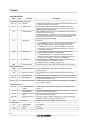
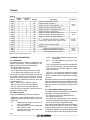
PIN DESCRIPTION
Name
Type
Function
Description
MICROPROCESSOR INTERFACE
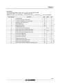
D (0 : 15)
I/O
Data Bus
These sixteen bidirectional pins provide communication with either an 8
or 16-bit host microprocessor data bus.
A (0 : 7)
I
Address Bus
These eigth pins select the internal register to be accessed. The
address can be latched by AE for direct connection to address/data
multiplexed microprocessor busses.
AE
I
Address Enable
When TS68483 is connected to a non-multiplexed microprocessor bus,
this input must be wired to VCC.
For direct connection to a multiplexed microprocessor bus, the falling
edge of AE latches the address on A (0 : 7) pins and the CS input. With
an Intel type microprocessor, AE is connected to the processor
Address Latch Enable (ALE) signal.
DS
I
Data Strobe
Active Low
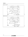
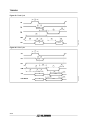
- In non-multiplexed bus mode, DS low enables the bidirectionnal data
buffers and latches the A (0 : 7) lines on its high to low transition.
Data to be written are latched on the rising edge of this signal.
- In multiplexed bus mode, this signal low enables the output data
buffers during a read cycle. With intel microprocessors, this pin is
connected to the RD signal.
R/W
I
Read/Write
- In non-multiplexed bus mode, this signal controls the direction of
data flow through the bidirectional data buffers.
- In multiplexed bus mode, this signal low enables the input data
buffers. The entering data are latched on its rising edge. With Intel
microprocessors, this pin is connected to the WR signal.
CS
I
Chip Select
This input selects the TS68483 registers for the current bus cycle. A
low level corresponds to an asserted chip select.
In multiplexed mode, this input is strobed by AE.
IRQ
O
Interrupt Request
This active-low open drain output acts to interrupt the microprocessor.
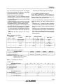
MEMORY INTERFACE
ADM
(0 : 15)
I/O
Address/Data Memory
These multiplexed pins act as address and data bus for display
memory interface.
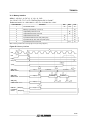
CYS
O
Memory Cycle Start
The falling edge of this output indicates the beginning of a memory
cycle.
Y (0 : 2)
O
Memory Address
These outputs provide the least significant bits of the Y logical address.
B (0 : 1)
O
Bank Number
These outputs provide the number of the memory bank to be accessed
during the current memory cycle.
CYF (0 : 1)
O
Memory Cycle Status
These outputs indicate the nature of the current memory cycle (Read,
Write, Refresh, Display).
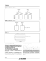
VIDEO INTERFACE
P (0 : 3)
O
Video Shift Register
Outputs
These four pins correspond to the outputs of the internal video shift
registers.
PC/HS
O
Phase Comparator/
Horizontal Sync.
This output can be programmed to provide either the phase comparator
output or the horizontal sync. signal.
HVS/VS
O
Composite or Vertical
Sync.
This output can be programmed to provide either the composite sync.
signal or the vertical sync. signal.
SYNC IN
I
External Sync Input
This input receives an external composite sync. signal to synchronize
TS68483. This input must be grounded if not used.
BLK
O
Blanking
This output provides the blanking interval information.
VCC
S
Power Supply
+ 5 V Supply
VSS
S
Ground
Ground
CLK
I
Clock
Clock Input
2/30
68483-01.TBL
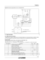
OTHER PINS