1
TS68483A
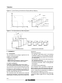
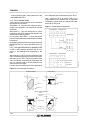
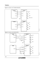
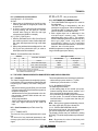
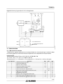
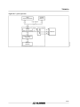
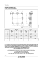
Figure 20 : Memory Organization for 512 x 384 Application
ADM [8:15]
B [0:1]
Y [0:2]
2
ADM [0:7]
3
Y
X
CYCLE
CONTROLLER
LATCH
BANK ENABLE
CAD0
ADSEL
MUX
DATA
Z1/Z3
DATA
Z0/Z2
8
64K x 8
64K x 8
MEMORY
ADDRESS
RAS
CAS
OE
WE
BANK 0
64K x 8
64K x 8
Z1
Z1 + 2
BANK 3
384
64K x 8 MEMORY BLOCK
128
One Block through Page Mode
SPARED AREA
68483-22.EPS
512
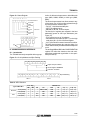
VI - TIMING DIAGRAM
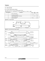
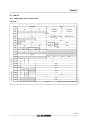
VI.1 - Microprocessor Interface
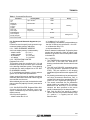
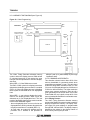
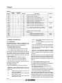
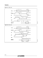
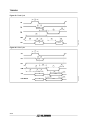
TS68483 has an eight bit address bus and a sixteen bit data bus. Little external logic is needed to adapt
bus control signals from most of the common multiplexed or non-multiplexed bus microprocessors.
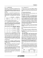
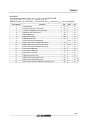
Indent Number
1
2
3
4
5
6
7
8
9
10
11
12
Parameter
Address Set up Time from CS
Data Strobe Width (high)
AS Set up Time from CS
Data Strobe Width-low (read cycle)
Address Hold Time from DS
Data Access time from CS (read cycle)
DS Inactive to High Impedance State (read cycle)
R/W Set up Time from DS
DS Width-low (write cycle)
CS Set up Time from DS Active (write Cycle)
Data in Set up Time from DS active (write cycle)
Data in Hold Time from DS Inactive (write cycle)
Min.
0
65
0
160
0
10
20
80
0
10
15
Max.
130
80
Unit
ns
ns
ns
ns
ns
ns
ns
ns
ns
ns
ns
ns
21/30
68483-11.TBL
UNMUX MODE
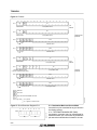
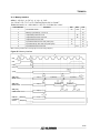
Microprocessor Interface Timing : A(0:7), D(0:15), AE, DS, CS, R/ W
VCC = 5.0V ± 5%, TA = TL to TH , CL = 100pF on D(0:15)
Reference levels : VIL = 0.8V and VIH = 2V on all inputs, VOL = 0.4V and VOH = 2.4V on all outputs