1
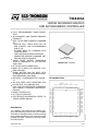
TS68483A
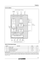
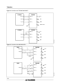
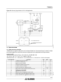
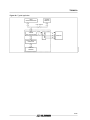
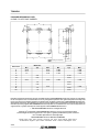
BLOCK DIAGRAM
MICROPROCESSOR INTERFACE
AE, DS
D [0: 15]
R/W, CS
4
A [0:7]
IRQ
8
16
38
R4
R0
R1
R2
R10
R3
43
CLK
2
BLK
5
PC/HS
4
HVS/VS
R12
VIDEO
VIDEO
3 SYNC IN
TIMING
V SS
INTERFACE
GENERATOR
52
R23
ADDRESS
VCC
19
DRAWING
VIDEO
AND
ACCESS
SHI FT
PROCESSOR
REGISTERS
P [0:3]
21
DATA
32
DATA
32
DISPLAY MEMORY LOGIC
65
CYS
CYF [0:1]
3
2
B [0:1]
Y [0:2]
16
68483-02.EPS
2
ADM [0:15]
DISPLA Y MEMORY INTERFACE
Symbol
Value
Unit
VCC*
Supply Voltage
Parameter
– 0.3, 7.0
V
Vin*
Input Voltage
– 0.3, 7.0
V
TA
Operating Temperature Range
0, 70
°C
Tstg
Storage Temperature Range
– 55, 150
°C
PDm
Max Power Dissipation
1.5
W
* With respect to VSS.
Stresses above those hereby listed may cause permanent damage to the device. The ratings are stress ones only and functional operation of
the device at these or any conditions beyond those indicated in the operational sections of this specifications is not implied. Exposure to maximum
rating conditions for extended periods may affect device reliability. Standard MOS circuits handling procedure should be used to avoid possible
damage to the device.
3/30
68483-02.TBL
ABSOLUTE MAXIMUM RATINGS