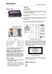
1
APPLICATION NOTE
Application of the TEA1099
Speech and Handsfree IC
with auxiliary inputs/output
and analog multiplexer
AN98061
Philips
Semiconductors
Philips Semiconductors
TEA1099 Speech and Handsfree IC with
Application Note
auxiliary inputs/output and analog multiplexer
Abstract
The TEA1099 is a bipolar circuit which includes line interface, speakerphone function and switches for
connection of auxiliary interfaces.It is intended to be used in line or mains powered telephone terminals.
A detailed description of the circuit blocks of the TEA1099 and advices on adjustments are contained in this
report.
2
Philips Semiconductors
TEA1099 Speech and Handsfree IC with
auxiliary inputs/output and analog multiplexer
APPLICATION NOTE
Application of the TEA1099
Speech and Handsfree IC
with auxiliary inputs/output
and analog multiplexer
AN98061
Authors:
D. Delbecq, A. Gauthier, J-M. Malaurie
Business Line Communication
Caen, France
Keywords
Telecom
Demonstration Board
TEA1099
transmit
receive
auxiliary
line
Date: June 11th, 1998
3
Application Note
Philips Semiconductors
TEA1099 Speech and Handsfree IC with
Application Note
auxiliary inputs/output and analog multiplexer
Summary
A detailed description of the TEA1099 is given.
The TEA1099 incorporates a line interface block with microphone, earphone and DTMF amplifiers.
It incorporates also a duplex controller with signal and noise monitors on the transmit and receive channels, a
base microphone amplifier as well as a loudspeaker amplifier.
In addition, two auxiliary inputs and one auxiliary output combined with integrated switches allow the use of the
TEA1099 in a lot of applications which can be either line-powered or powered from the mains.
A cookbook gives the general application steps.
A demonstration board, OM5846, is available.
Note :
The information presented in this document does not form part of any quotation or contract, is believed to be
accurate and reliable and may be changed without notice. No liability will be accepted by the publisher for any
consequence of its use. Publication thereof does not convey nor imply any licence under patent or other
industrial or intellectual property rights.
4
Philips Semiconductors
TEA1099 Speech and Handsfree IC with
Application Note
auxiliary inputs/output and analog multiplexer
CONTENTS
1. INTRODUCTION ..................................................................................................................................... 8
2. BLOCK DIAGRAM ................................................................................................................................ 10
3. DESCRIPTION OF THE TEA1099......................................................................................................... 16
3.1 Line interface................................................................................................................................... 16
3.1.1 DC characteristics ................................................................................................................. 16
3.1.2 Line impedance ..................................................................................................................... 21
3.1.3 Anti-sidetone network ............................................................................................................ 22
3.1.4 Automatic gain control ........................................................................................................... 23
3.2 Supplies .......................................................................................................................................... 24
3.2.1 Supply VBB ........................................................................................................................... 25
3.2.2 Supply VDD........................................................................................................................... 28
3.2.3 Microphone supply MICS....................................................................................................... 29
3.3 Transmit.......................................................................................................................................... 29
3.3.1 Handset microphone amplifier ............................................................................................... 31
3.3.2 DTMF amplifier...................................................................................................................... 34
3.3.3 Handsfree microphone channel ............................................................................................. 36
3.3.4 Auxiliary transmit amplifier TXAUX ........................................................................................ 38
3.4 Receive........................................................................................................................................... 40
3.4.1 Line receive amplifier RECO.................................................................................................. 41
3.4.2 Earphone amplifier QR .......................................................................................................... 45
3.4.3 Loudspeaker amplifier LSAO ................................................................................................. 46
3.4.4 Auxiliary receive amplifier AUXO ........................................................................................... 48
3.4.5 Auxiliary microphone monitor amplifier................................................................................... 53
3.5 Duplex controller ............................................................................................................................. 53
3.5.1 Signal and noise envelope detectors...................................................................................... 54
3.5.2 Decision logic ........................................................................................................................ 55
3.5.3 Voice switch .......................................................................................................................... 56
3.5.4 Adjustments and performances of the duplex controller ......................................................... 57
3.6 Logic block ...................................................................................................................................... 63
3.6.1 Logic inputs ........................................................................................................................... 63
3.6.2 Connections .......................................................................................................................... 64
4. APPLICATION COOKBOOK ................................................................................................................ 67
5. APPLICATION EXAMPLES .................................................................................................................. 71
6. ELECTROMAGNETIC COMPATIBILITY .............................................................................................. 80
7. REFERENCES ...................................................................................................................................... 81
5
Philips Semiconductors
TEA1099 Speech and Handsfree IC with
Application Note
auxiliary inputs/output and analog multiplexer
LIST OF FIGURES
Fig. 1 Handsfree telephone set principle............................................................................................................ 8
Fig. 2 Block diagram of TEA1099 ................................................................................................................... 10
Fig. 3 Pinning of TEA1099 ............................................................................................................................. 11
Fig. 4 Table of switch management................................................................................................................ 15
Fig. 5 DC characteristics configuration ........................................................................................................... 17
Fig. 6 Ibb versus Vbb ..................................................................................................................................... 18
Fig. 7 Main voltages versus line current.......................................................................................................... 18
Fig. 8 Low voltage behavior in line powered condition..................................................................................... 19
Fig. 9 Low voltage behavior when VBB = 5 V ................................................................................................. 19
Fig. 10 Influence of the Rva resistor between REG and SLPE on Vln at 15 mA.............................................. 20
Fig. 11 Influence of Rslpe on the DC characteristics....................................................................................... 21
Fig. 12 Equivalent set impedance................................................................................................................... 21
Fig. 13 Anti-sidetone bridge connection.......................................................................................................... 22
Fig. 14 Equivalent average line impedance..................................................................................................... 23
Fig. 15 AGC on the microphone gain versus line current and Ragc ................................................................ 24
Fig. 16 Block diagram of the supply block....................................................................................................... 25
Fig. 17 Loudspeaker output power versus line current .................................................................................... 26
Fig. 18 Current consumption on VBB in "ring mode" versus VBB.................................................................... 28
Fig. 19 Current consumption on VDD at VBB = 0 ........................................................................................... 29
Fig. 20 Block diagram of the transmit part ...................................................................................................... 30
Fig. 21 Handset microphone gain versus frequency: influence of temperature ................................................ 32
Fig. 22 Distortion on line versus handset microphone signal on TEA1099........................................................ 32
Fig. 23 Distortion of line signal at Iline = 4 mA ................................................................................................ 33
Fig. 24 Handset microphone noise versus line current.................................................................................... 33
Fig. 25 Common mode rejection ratio on microphone ..................................................................................... 34
Fig. 26 DTMF gain versus frequency: influence of the temperature ................................................................ 35
Fig. 27 Distortion of the DTMF signal on line versus input signal .................................................................... 35
Fig. 28 Connection of the handsfree electret microphone ................................................................................ 37
Fig. 29 Distortion on line versus HFTX input level........................................................................................... 38
Fig. 30 Distortion on line versus TXAUX input signal ...................................................................................... 39
Fig. 31 Transmit noise versus line current ....................................................................................................... 39
Fig. 32 Receive block diagram ....................................................................................................................... 40
Fig. 33 Block diagram related to AUXO .......................................................................................................... 41
Fig. 34 Receive gain versus frequency: influence of temperature ................................................................... 43
Fig. 35 Distortion on RECO versus input signal on IR..................................................................................... 43
Fig. 36 Distortion on RECO versus input signal on RAUX............................................................................... 44
Fig. 37 Distortion on RECO versus level with 5 kΩ load ................................................................................. 44
Fig. 38 Noise on RECO.................................................................................................................................. 45
Fig. 39 Distortion on QR versus level ............................................................................................................. 46
Fig. 40 Output level in ring mode versus input current at ESI......................................................................... 48
Fig. 41 Auxiliary receive gain versus frequency, influence of temperature....................................................... 50
Fig. 42 Distortion on AUXO versus input signal on IR ..................................................................................... 50
Fig. 43 Distortion on AUXO versus input signal on HFRX ............................................................................... 51
Fig. 44 Distortion on AUXO versus input signal on HFTX ............................................................................... 51
Fig. 45 Distortion on AUXO versus level with 5 kΩ load.................................................................................. 52
Fig. 46 Noise on AUXO with input at IR.......................................................................................................... 52
Fig. 47 Noise on AUXO with input at MIC+/MIC- ............................................................................................ 53
6
Philips Semiconductors
TEA1099 Speech and Handsfree IC with
Application Note
auxiliary inputs/output and analog multiplexer
Fig. 48 Principle of the duplex controller ......................................................................................................... 54
Fig. 49 Typical behavior of the signal and noise detectors .............................................................................. 55
Fig. 50 Truth table of the decision logic .......................................................................................................... 56
Fig. 51 Behavior of the voice switch ............................................................................................................... 57
Fig. 52 Circuit for shifting the idle mode.......................................................................................................... 61
Fig. 53 GND and GNDTX connections ........................................................................................................... 62
Fig. 54 Table of connections .......................................................................................................................... 65
Fig. 55 Steps in the design flow of the TEA1099 ........................................................................................... 70
Fig. 56 Basic handsfree application ................................................................................................................ 72
Fig. 57 Group-listenning conversation with antihowling................................................................................... 73
Fig. 58 Cordless: conference with line, base and mobile................................................................................. 74
Fig. 59 Cordless: handsfree conversation in mobile ........................................................................................ 75
Fig. 60 Answering Machine on line ................................................................................................................. 76
Fig. 61 Cordless intercom between mobile and base handset.......................................................................... 77
Fig. 62 Application with Fax, Cordless and Answering Machine ...................................................................... 78
Fig. 63 Typical external antihowling circuit...................................................................................................... 79
Fig. 64 Schematic of the demoboard ............................................................................................................... 86
Fig. 65 component placement diagram of the demoboard............................................................................... 87
Fig. 66 Curve ref board of the TEA1099 ......................................................................................................... 88
7
Philips Semiconductors
TEA1099 Speech and Handsfree IC with
Application Note
auxiliary inputs/output and analog multiplexer
1. INTRODUCTION
The TEA1099 is a circuit which offers a handsfree function with the line interface and the normal handset
interface, it also incorporates auxiliary amplifiers combined with switches and a logic control block.
It incorporates a base microphone amplifier, a volume control of the loudspeaker amplifier and a duplex
controller with signal and noise monitoring on the transmit and receive channels.
A power supply block extracts power from the line in an optimized way for the loudspeaker amplifier;
furthermore, this supply block can be powered from any external supply. A stabilized 3.35 V supply is available
for peripherals.
This makes the TEA1099 suitable as the core of a multifunction telecom terminal, such as cordless telephones,
answering machines or fax machines.
The function of the handsfree application is illustrated with the help of fig.1.
Line
HYBRID
DUPLEX CONTROL
acoustic
coupling
sidetone
Fig. 1 Handsfree telephone set principle
The left side of fig. 1 shows a principle diagram of the line interface part of the TEA1099 circuit by means of a
receiving preamplifier, a transmit amplifier and the hybrid. The right side of fig.1 shows a principle diagram of
the handsfree part of the TEA1099 circuit by means of the microphone preamplifier, the loudspeaker amplifier
and the duplex controller.
As can be seen from fig. 1, a closed loop is formed via the amplifiers, the antisidetone network and the
acoustic coupling between loudspeaker and microphone. When the loop-gain is higher than one, the set starts
8
Philips Semiconductors
TEA1099 Speech and Handsfree IC with
Application Note
auxiliary inputs/output and analog multiplexer
howling. In a full-duplex application, this would be the case. To avoid howling, the duplex controller reduces the
loop-gain to a value much lower than one.
The duplex controller of the TEA1099 monitors the signal and noise on both the transmit and the receive
channel in order to detect which channel contains the ‘largest’ signal. As a result, the duplex controller reduces
the gain of the channel which contains the smallest signal. The sum of the transmit and the receive gains
remains constant.
As a result, the circuit can be in three stable modes to be referred to throughout this report:
1.
2.
3.
Transmit mode (Tx-mode): the gain of the handsfree microphone path is at its maximum and the gain of
the receive path (to loudspeaker amplifier) is reduced.
Receive mode (Rx-mode): the gain of the receive path is at its maximum and the gain of the
microphone amplifier is reduced.
Idle mode (Ix-mode): the gains of the handsfree microphone path and of the receive path are halfway
their maximum and reduced values.
The difference between the maximum gain and the reduced gain is called the switching range.
This report gives a detailed description of the TEA1099 and its basic application. The description is given by
means of the block diagram of the TEA1099 (§2) and by discussing every detail of the sub-blocks (§3). The
application is discussed by giving a guideline for application (the application cookbook §4) and by giving an
application example (§5). EMC aspects are also discussed (§6). The appendix contains a list of abbreviations
and the demoboard application diagram of the TEA1099.
Note: the values of parameters given in this application note are as accurate as possible, but please, refer to
the last product specification for final ones.
9
Philips Semiconductors
TEA1099 Speech and Handsfree IC with
Application Note
auxiliary inputs/output and analog multiplexer
2. BLOCK DIAGRAM
In this chapter, the block diagram of the TEA1099 is shown by means of fig. 2. The pinning of the TEA1099
is given by means of fig. 3. A short description of the block diagram is given including the function of the
external components.
LOGIC
INPUTS
PD/
3.3 V µC supply
HFC
from µC or
dialler
POWER SUPPLY
VDD
to µC or
dialler
GNDTX
GND
MUTT/
Power supply
MUTR/
VBB
ESI
AUXC
REG
REFERENCE
STAB
LINE
INTERFACE
AGC
LN
SLPE
TXAUX
DTMF
TRANSMIT
MIC+
MICSWT
HFTX
IDT
TXOUT
SWR
GATX
TSEN
TXIN
TENV
TNOI
MICS
DUPLEX
CONTROLLER
reg.
HFRX
RNOI
RENV
RSEN
VBB
GAIN
CONTROL
VOL
DLC
GALS
LSAO
IR
AUXO
RECO
RAUX
GARX
RECEIVE
QR
Fig. 2 Block diagram of TEA1099
10
Z
Philips Semiconductors
TEA1099 Speech and Handsfree IC with
Application Note
GARX
RECO
HFTX
HFC
PD/
MTTT/
MUTR/
AUXC
RAUX
TXAUX
AUXO
auxiliary inputs/output and analog multiplexer
44 43 42 41 40 39 38 37 36 35 34
HFRX
1
33
QR
TNOI
2
32
DTMF
TENV
3
31
MIC+
TSEN
4
30
MIC-
RNOI
5
29
GNDTX
RSEN
6
28
TXIN
RENV
7
27
GATX
DLC
8
26
TXOUT
ESI
9
25
IDT
VBB
10
24
SWT
23
VOL
SWR
STAB
MICS
VDD
AGC
IR
REG
LN
SLPE
13 14 15 16 17 18 19 20 21 22
GND
11
12
LSAO
GALS
TEA1099
Fig. 3 Pinning of TEA1099
PIN
NAME
DESCRIPTION
1
HFRX
Receive input for loudspeaker amplifier or auxiliary receive amplifier
2
TNOI
Transmit noise envelope timing adjustment
3
TENV
Transmit signal envelope timing adjustment
4
TSEN
Transmit signal envelope sensitivity adjustment
5
RNOI
Receive noise envelope timing adjustment
6
RSEN
Receive signal envelope sensitivity adjustment
7
RENV
Receive signal envelope timing adjustment
8
DLC
Dynamic limiter
9
ESI
External supply input
10
VBB
Stabilized supply for internal circuitry
11
GALS
Loudspeaker amplifier gain adjustment
12
LSAO
Loudspeaker amplifier output
13
GND
Ground reference
14
SLPE
Line current sense
11
Philips Semiconductors
TEA1099 Speech and Handsfree IC with
auxiliary inputs/output and analog multiplexer
15
16
LN
REG
Positive line terminal
Line voltage regulator decoupling
17
IR
Receive channel input
18
AGC
Automatic gain control
19
VDD
3.35 V supply voltage
20
MICS
Supply for electret microphones
21
STAB
Reference current adjustment
22
SWR
Switching range adjustment
23
VOL
Loudspeaker amplifier volume adjustment
24
SWT
Switching timing adjustment
25
IDT
Idle-mode timing adjustment
26
TXOUT
Handsfree microphone amplifier output
27
GATX
Handsfree microphone gain adjustment
28
TXIN
Handsfree microphone amplifier input
29
GNDTX
Ground reference for microphone amplifiers
30
MIC-
Inverting HS microphone input
31
MIC+
Non-inverting HS microphone input
32
DTMF
Dual Tone Multifrequency input
33
QR
Earpiece amplifier output
34
GARX
Earpiece amplifier gain adjustment
35
RECO
Receive amplifier output
36
HFTX
Transmit input for line amplifier or auxiliary receive amplifier
37
HFC
Logic input
38
PD/
Power-down input
39
MUTT/
Logic input
40
MUTR/
Logic input
41
AUXC
Logic input
42
RAUX
Auxiliary receive input
43
TXAUX
Auxiliary transmit input
44
AUXO
Auxiliary output
12
Application Note
Philips Semiconductors
TEA1099 Speech and Handsfree IC with
Application Note
auxiliary inputs/output and analog multiplexer
In fig. 2 it can be seen that the IC consists out of six main parts: the line interface, the supply block, the
transmit block, the receive block with the loudspeaker amplifier, the duplex controller and the logic block which
controls the IC. These blocks are shortly described below including the function of the external components.
The detailed description will follow in chapter 3.
Line interface :
The TEA1099 generates a stabilized voltage (called Vref) between pins GND and SLPE. This reference voltage
is line current dependant in order to get optimum supply for the loudspeaker amplifier and is stabilized by the
capacitor Creg connected at pin REG. The line current is sensed across the resistor connected between pins
LN and SLPE.
An AGC function is provided when pin AGC is connected directly or through a resistor to LN.
The impedance of the apparatus is set by a network connected between LN and GND through a decoupling
capacitor.
Supply:
The circuit can be supplied from the line and/or by an external supply. It provides a stabilized 3.35 V supply
point for peripherals which can also be externally supplied in trickle mode. The TEA1099 can be switched into a
low power consumption mode with the pin PD/.
Transmit:
The transmit signal can come from four preamplifiers: handset microphone (MIC+/MIC-), handsfree microphone
(TXIN to TXOUT and HFTX), the auxiliary transmit (TXAUX) and the DTMF. The selection is made by the logic
block.The signal reference is GNDTX, a “clean ground” which has to be connected to GND, for the handsfree
microphone. The inputs have to be coupled by means of capacitors. All the gains have a fixed value except the
gain of the handsfree microphone amplifier which is set with Rgatx.
Receive:
The signal received from the line is amplified from pin IR to pin RECO and/or to the auxiliary output AUXO. The
input IR has to be coupled by means of a capacitor. From pin RECO, the signal is sent to the earphone
amplifier at pins GARX and QR and to the input of the duplex controller HFRX. The gain of the earphone
amplifier is set with 2 resistors. From HFRX, the signal can be sent to the loudspeaker amplifier (pins GALS and
LSAO) and the volume can be adjusted by means of the potentiometer connected between input VOL and
GNDTX, the gain of the loudspeaker amplifier is set by the resistor Rgals. The signal from the auxiliary input
RAUX can also be sent to RECO.
Moreover the auxiliary output AUXO can get its signal from IR, HFRX through the duplex controller, MIC+/MICor HFTX.
Duplex controller:
From both the transmit and receive signals, signal and noise envelopes are made. The transmit signal envelope
is on pin TENV and the receive one on pin RENV. The transmit noise envelope is on pin TNOI and the receive
one on pin RNOI. The timing of the envelopes can be set by the capacitors Ctenv, Ctnoi, Crenv and Crnoi. The
sensitivity of the envelope detectors can be set by means of the RC combinations Rtsen with Ctsen for the
13
Philips Semiconductors
TEA1099 Speech and Handsfree IC with
Application Note
auxiliary inputs/output and analog multiplexer
transmit envelope and Rrsen with Crsen for the receive one. The resistors set the sensitivity and the capacitors
block the DC-component, creating also high-pass filters.
The decision logic of the duplex controller determines into which mode (Tx, Rx or Ix-mode) the set has to switch
over. The timing for switching to the Tx or the Rx -mode is determined with the capacitor Cswt. The timing for
switching to the Ix-mode is set by the combination Cswt and Ridt. The switching range is determined by the
resistor Rswr. Resistor Rstab has a fixed value.
Logic block :
The logic block manages the internal switches according to the following table.
14
Philips Semiconductors
TEA1099 Speech and Handsfree IC with
Application Note
auxiliary inputs/output and analog multiplexer
LOGIC INPUTS
CONNECTIONS
MODES
(PD/)
HFC
MUTT/ MUTR/ AUXC
0
X
X
X
1
0
X
X
X
0
1
0
0
0
0
DTMF->LN ; CT->RECO
(MICS, QR)
1
0
0
1
0
MIC->AUXO; RAUX->RECO
(MICS, QR)
1
0
0
1
1
MIC->AUXO; RAUX->RECO
(QR)
1
0
1
X
0
MIC->LN; IR->RECO; IR->AUXO Handset conversation
MIC->TXOUT
(MICS, QR)
1
0
1
1
1
MIC -> LN; MIC -> TXOUT
(QR)
1
0
1
0
1
TXAUX->LN ; IR->AUXO
1
0
0
0
1
TXAUX->LN ; IR->AUXO
RAUX -> RECO
1
1
1
1
1
TXIN->TXOUT; HFTX->LN;
IR->RECO; HFRX->AUXO
1
1
0
1
1
RAUX->RECO; HFRX->LSAO
1
1
0
0
1
TXAUX->LN ; IR->AUXO ;
RAUX->RECO; HFRX->LSAO
1
1
0
0
0
DTMF->LN ; CT->RECO;
HF/GL Tel Set DTMF
HFRX->LSAO
( MICS, QR) dialling
1
1
1
0
1
TXAUX->LN ; IR->AUXO ;
IR->RECO; HFRX->LSAO
1
1
0
1
0
TXIN->TXOUT; HFTX->AUXO;
RAUX->RECO; HFRX->LSAO
(MICS)
1
1
1
1
0
TXIN->TXOUT; HFTX->LN;
Handsfree conversation
IR->RECO; IR->AUXO;
HFRX->LSAO
(MICS)
1
1
1
0
0
Group-listenning
MIC->LN; IR->RECO;
conversation
IR->AUXO; HFRX->LSAO
MIC->TXOUT
(MICS,QR)
HFRX -> LSAO
Ring mode
Flash, DC dialling
Fig. 4 Table of switch management
15
Tel. Set: DTMF dialling
Conversation with auxiliary
Philips Semiconductors
TEA1099 Speech and Handsfree IC with
Application Note
auxiliary inputs/output and analog multiplexer
3. DESCRIPTION OF THE TEA1099
This chapter describes in detail the six blocks of the speech/handsfree circuit TEA1099: the line interface (3.1),
the supply (3.2), the transmit block (3.3), the receive block (3.4), the duplex controller (3.5) and the logic block
(3.6). For each block the principle of operation is described and its adjustments and performances are
discussed.
All values given in this chapter are typical and at room temperature unless otherwise stated. For more details,
see TEA1099 device specification.
All the curves shown in this section result from measurement of typical samples using the schematic of fig. 66.
All the component names refer to the basic application of the IC shown in appendix fig. 64.
3.1
3.1.1
Line interface
DC characteristics
Principle of operation
The TEA1099 generates a stabilized voltage (called Vref) between pins GND and SLPE. This reference
voltage, temperature compensated, is typically 3.7 V for line currents between 10 and 18 mA and 6.15 V for line
currents between 46 and 140 mA. For line currents between 18 and 46 mA, Vref increases proportionally to this
line current with a slope of typically 87.5 Ω so, from typically 3.7 to 6.15 V. The voltage at pin REG is used by
the internal regulator to generate the stabilized Vref voltage and is decoupled by a capacitor Creg connected to
LN.
For effective operation of the apparatus, the TEA1099 must have a low resistance to the DC current and a high
impedance to speech signals. The Creg capacitor, converted into an equivalent inductance (see “set
impedance” section), realizes this impedance conversion from its DC value (Rslpe) to its AC value (Zimp in the
audio frequency range). The DC voltage between pins LN and SLPE is proportional to the line current.
This general configuration is shown in fig. 5.
16
Philips Semiconductors
TEA1099 Speech and Handsfree IC with
Application Note
auxiliary inputs/output and analog multiplexer
Rline
Iline
Zimp
Islpe
Iln
+ Creg
LN
Rexch
REG
+
Rslpe
Cimp
SLPE
Starter
Vd
Vexch
Supply
block
Iline management
slope
low voltage
Switch
Rp
GND
from transmit
preamps
Fig. 5 DC characteristics configuration
The IC regulates the line voltage between pins GND and SLPE. The voltage on pin LN can be calculated as:
Vln = Vref + Rslpe × Islpe
Islpe = Iline - Iln
Iline = line current
Iln = current consumption between LN and GND
Between 18 and 46 mA:
Vref ≅ 3.7 + ( Islpe - 18 mA ) × 87.5
The DC line current Iline flowing into the apparatus is determined by the exchange supply voltage Vexch, the
feeding bridge resistance Rexch, the DC resistance of the telephone line Rline and the voltage across the
telephone set including diode bridge.
Below a threshold line current Ith (typically equal to 9 mA) the internal reference voltage (generating Vref) is
automatically adjusted to a lower value (down to an absolute minimum voltage of 1.6 V). This means that more
sets can operate in parallel or that for very low voltage feeding bridge the line current has a higher value. For
line currents below this threshold current, the TEA1099 has reduced sending and receiving performances. This
is called the low voltage area.
The internal circuitry of the TEA1099 is supplied from pin VBB. In line powered application, this voltage is
derived from the line voltage by the supply block and must be decoupled by a capacitor (Cvbb). Fig. 6 shows
17
Philips Semiconductors
TEA1099 Speech and Handsfree IC with
Application Note
auxiliary inputs/output and analog multiplexer
the IC current consumption (Ibb) as a function of the VBB supply voltage in handset mode and in handsfree
mode.
Ibb (mA)
10
9
handsfree mode
8
7
6,57
handset mode
6
5
4
3
3,5
4
4,5
5
5,5
VBB (V)
Fig. 6 Ibb versus Vbb
Fig. 7 shows the main voltages as a function of the line current in line powered conditions.
(V)
10
VLN
9
8
7
VSLPE
6
VBB
5
4
VDD
3
VMICS
2
1
0
000,E+0
20,E-3
40,E-3
60,E-3
80,E-3
100,E-3
120,E-3
140,E-3
Iline (A)
Fig. 7 Main voltages versus line current
18
Philips Semiconductors
TEA1099 Speech and Handsfree IC with
Application Note
auxiliary inputs/output and analog multiplexer
Fig. 8 shows the behavior in the low voltage area in line powered condition.
(V)
VLN
4
VSLPE
3,5
VBB
3
VDD
2,5
VMICS
2
1,5
1
0,5
0
000,E+0
2,E-3
4,E-3
6,E-3
8,E-3
10,E-3
12,E-3
14,E-3
16,E-3
Iline (A)
Fig. 8 Low voltage behavior in line powered condition
Fig. 9 shows the behavior in the low voltage area when VBB is externally supplied at 5 V.
(V)
6
VBB
5
VLN
4
VDD
VSLPE
3
VMICS
2
1
0
000,E+0
2,E-3
4,E-3
6,E-3
8,E-3
10,E-3
12,E-3
14,E-3
Iline (A)
Fig. 9 Low voltage behavior when VBB = 5 V
19
Philips Semiconductors
TEA1099 Speech and Handsfree IC with
Application Note
auxiliary inputs/output and analog multiplexer
Adjustments and performances
The reference voltage, Vref, can be adjusted by means of an external resistor Rva. It can be increased by
connecting the Rva resistor between pins REG and SLPE (Fig. 10), or decreased by connecting the Rva
resistor between pins REG and GND. In line powered application, it is possible to use the voltage reduction only
for less than 300 mV because it reduces the VBB supply capability, this reduction is easier when VBB is
provided by an external 5 V power supply. To ensure correct operation, it is not advised to adjust Vref at a value
lower than 3.3 V at 18 mA or higher than 7 V at a maximum line current of 90 mA (the maximum operating
voltage of 12 V must be guaranteed by the application as well as the safe crystal operating temperature). These
adjustments will slightly affect a few parameters: there will be a small change in the temperature coefficient of
Vref and a slight increase in the spread of this voltage reference due to matching between internal and external
resistors. Furthermore, the Rva resistor connected between REG and GND will slightly affect the apparatus
impedance (see section “set impedance”).
VLN (V)
14
12
10
8
6
4
2
0
1,E+3
10,E+3
100,E+3
1,E+6
R(SLPE-REG) (ohms)
Fig. 10 Influence of the Rva resistor between REG and SLPE on Vln at 15 mA
The DC slope of the voltage on pin LN is influenced by the Rslpe resistor as shown in fig. 11. This value of
Rslpe may be slightly modified even if the preferred one is 20 Ω; changing this value will affect more than the
DC characteristics, it also influences the gains, the AGC characteristics, the maximum output swing on the line,
the VBB slope start and stop currents and the low voltage threshold Ith.
20
Philips Semiconductors
TEA1099 Speech and Handsfree IC with
Application Note
auxiliary inputs/output and analog multiplexer
VLN (V)
10
9
30 ohms
8
7
6
20 ohms
10 ohms
5
4
3
2
1
0
000,E+0
10,E-3
20,E-3
30,E-3
40,E-3
50,E-3
60,E-3
70,E-3
80,E-3
90,E-3
100,E-3
Iline (A)
Fig. 11 Influence of Rslpe on the DC characteristics
3.1.2
Line impedance
Principle of operation
The TEA1099 behaves like an equivalent inductance that presents a low impedance to DC and a high
impedance (Rp) to speech signals. Rp is an integrated resistance in the order of 25 kΩ +/-15%. It is in parallel
with the external network realized by Zimp and Cimp. Thus, in the audio frequency range, the apparatus
impedance (called set impedance) is mainly determined by the Zimp resistor. Fig. 12 shows an equivalent
schematic for the set impedance.
LN
Rslpe
20 Ω
SLPE
Leq
Vref
Zimp
+
Creg
4.7 µF
Leq = Creg x Rslpe x Rp
Rp = internal resistor
REG
+
Cimp
Rp
22 µF
GND
Fig. 12 Equivalent set impedance
21
Philips Semiconductors
TEA1099 Speech and Handsfree IC with
Application Note
auxiliary inputs/output and analog multiplexer
Adjustments and performances
When decreasing the reference voltage Vref, a resistor is connected between GND and REG in parallel of Rp
(see fig. 12) so, slightly modifying the impedance.
If complex set impedance is required Zimp is a complex network, if a purely resistive set impedance is required
Zimp is a resistor.
The value of the capacitor Cimp has to be high enough (advised value of 22 µF) in order to have an impedance
negligible compare to Zimp or it may be used to generate the capacitive part of a complex impedance assuming
that DC decoupling is kept.
3.1.3
Anti-sidetone network
Principle of operation
To avoid the microphone signal to come back with a too high level in the receive channel, the anti-sidetone
circuit uses the microphone signal from pin SLPE (which is in opposite phase) to cancel the microphone signal
at the IR input of the receive amplifiers. The anti-sidetone bridge principle already used for the TEA106x or the
TEA111x families is used in a reversed way for the design of the anti-sidetone network as shown in fig. 13.
GND
Rast1
Rcc
Zline
LN
Itr
IR
RECO/AUXO
Zir
Rast2
Rslpe
Rast3
SLPE
Zbal
Fig. 13 Anti-sidetone bridge connection
This anti-sidetone bridge has the advantage of a relative flat transfer function in the audio frequency range
between the line and the outputs RECO or AUXO, both with real and complex set impedances. Furthermore,
the attenuation of the bridge for the receive signal (between pins LN and IR) is independent of the value chosen
for Zbal after the set impedance has been fixed and the condition shown in equation (st) is fulfilled. Therefore,
readjustment of the overall receive gain is not necessary in many cases.
The anti-sidetone circuit is composed of: Rcc//Zline, Rast1, Rast2, Rast3, Rslpe and Zbal. Maximum
compensation is obtained when the following conditions are fulfilled:
Rslpe × Rast1 = Rcc × ( Rast2 + Rast3 )
(st)
k = [Rast2 × ( Rast3 + Rslpe )] / ( Rast1 × Rslpe )
Zbal = k × Zline
The scale factor k is chosen to meet the compatibility with a standard value of capacitor for Zbal.
22
Philips Semiconductors
TEA1099 Speech and Handsfree IC with
Application Note
auxiliary inputs/output and analog multiplexer
In practice, Zline varies strongly with line lenght and line type. Consequently, the value for Zbal has to be
chosen to fit with an average line length giving acceptable sidetone suppression with short and long lines. The
suppression further depends on the accuracy with which Zbal equals this average line impedance.
Example
Let’s optimize for a theorical equivalent average line impedance shown in Fig. 14.
1265 Ω
210 Ω
140 nF
Fig. 14 Equivalent average line impedance
For compatibility of the capacitor value in Zbal with a standard capacitor value from the E6 series (220 nF):
k = 140 / 220 = 0.636
For Rast2, a value of 3.92 kΩ has been chosen. So, using the previous equations, we can calculate Zbal,
Rast1, Rast3. We find Rast1 = 130 kΩ, Rast3 = 390 Ω, and for Zbal 130 Ω in series with 220 nF // 820 Ω.
The attenuation of the receive line signal between LN and IR can be derivated from the following equation:
Vir / Vln = ( Zir // Rast2 ) / [ Rast1 + ( Zir // Rast2 )]
If Rast2 >> ( Rast3 // Zbal ).
With the values used in this example, it gives 32 dB at 1 kHz.
Zir is the receive amplifier input impedance, typically 20 kΩ.
3.1.4
Automatic gain control
Principle of operation
The TEA1099 performs automatic line loss compensation. The automatic gain control varies the gains
(according to the line DC current) of the amplifiers which send on line, except the DTMF one, and of the
amplifiers which receive from line at pin IR. To enable this AGC function, the pin AGC must be connected to the
pin LN. For line currents below a current threshold, Istart (typically 23mA), the gain control factor α is equal to 1,
giving the maximum value to the gains. If this threshold current is exceeded, the gain control factor α is reduced
and then the gains of the controlled amplifiers are also reduced. When the line current reaches an other
threshold current, Istop (typically 57 mA), the gain control factor α is limited to its minimum value equal to 0.49
or 0.47, giving the lower value to the transmit and receive controlled gains. The gain control range of these
amplifiers is typically 6.2 dB or 6.6 dB depending on the amplifier (see datasheet), which corresponds
approximately to a line length of 5.5 km (0.5 mm twisted pair copper) with an attenuation of 1.2 dB/km.
The attenuation is correlated to the current Iagc sunk at pin AGC: when this current is lower than typically 4.8
µA the gains are maximum, when this current is higher than typically 12 µA the gains are minimum. This current
is proportional to the voltage between pins SLPE and LN. There is an internal resistor which sets Istart and
Istop, adding Ragc externally in series (between pins AGC and LN) reduces Iagc and increases the values of
Istart and Istop.
23
Philips Semiconductors
TEA1099 Speech and Handsfree IC with
Application Note
auxiliary inputs/output and analog multiplexer
Adjustments and performances
The AGC of the TEA1099 can be used with different exchange supply voltages and different feeding bridge
resistances. For this purpose, a resistor Ragc, can be inserted between pins AGC and LN. This Ragc resistor
increases the two threshold currents Istart and Istop. Fig.15 shows the control of the microphone gain versus
the line current for two values of Ragc. When no AGC function is required, the AGC pin must be left open, then
the control factor α equals to 1 and both controlled gains are at their maximum values.
When Ragc = 0 and the value of Istart is too high, increasing slightly the value of Rslpe reduces proportionally
Istart and shifts the AGC to lower currents but the gains, the DC characteristic and the value of VBB are also
modified. If the value of Rslpe has to be increased, it is possible to restore the typical gains (but not the value of
VBB) by connecting in parallel an RC series network which makes a total AC impedance of 20 Ω.
|mic to ln| (dB)
45
44
43
42
41
Ragc(ext) = 0
Ragc(ext)=81.5K
40
39
38
0,015
0,02
0,025
0,03
0,035
0,04
0,045
0,05
0,055
0,06
0,065
0,07
0,075
0,08
0,085
0,09
0,095
0,1
0,105
0,11
Iline (A)
Fig. 15 AGC on the microphone gain versus line current and Ragc
3.2
Supplies
The TEA1099 provides three supply points, VBB is the strong supply for most of the internal circuitry and the
amplifiers, VDD is a 3.35 V supply for the dialler or the microcontroller and MICS is a switched supply point for
the electret microphones. Moreover, the TEA1099 can be powered by an external power supply connected at
the input ESI.
Fig. 16 shows the block diagram of the supply block:
24
Philips Semiconductors
TEA1099 Speech and Handsfree IC with
Application Note
auxiliary inputs/output and analog multiplexer
from external
supply
+ Creg
LN
REG
Cvbb
Rslpe
+
VBB
SLPE
ESI
Starter
Vd
Bandgap
Iline management
slope
low voltage
Switch
Voltage
stabilizer
Rp
Supply
current
detection
VDD
VDD
voltage
supply
from external
supply
+
Cvdd
low VBB
condition detection
MICS
electret
microphone
supply
logic
+
Cmics
GND
Fig. 16 Block diagram of the supply block
3.2.1
Supply VBB
Principle of operation
VBB can be either line powered or externally powered at ESI, when both supplies are available, the strongest of
the two is automatically selected and used internally. When VBB is purely line powered, its value is correlated
with the value of the line voltage and then of the line current as follows:
• below 9 mA
: low voltage area
25
Philips Semiconductors
TEA1099 Speech and Handsfree IC with
Application Note
auxiliary inputs/output and analog multiplexer
• 9 to 18 mA
: VBB = 3 V
• 18 to 46 mA
: VBB increases with a slope of 84 Ω from 3 to 5.35 V
• above 46 mA
: VBB = 5.35 V
The correlation between line voltage and VBB is done in order to get a voltage difference between Vslpe and
VBB of at least 0.7 V in order to guarantee a good power supply efficiency when AC signal is present on SLPE.
On the block diagram, two PNP transistors drive the line current either to VBB or to GND: when the voltage on
SLPE is higher than VBB + 0.3 V the current is driven to VBB, when the voltage on SLPE is lower than VBB the
line current is driven to GND, when the voltage on SLPE is between VBB and VBB + 0.3 V both transistors are
conducting in order to minimize distortion.
The correlation between line voltage and line current is done in order to get the optimized correlation between
the power that can be extracted from the line and the power that can be delivered to the loudspeaker amplifier.
Fig. 7 shows these different voltages versus line current, fig. 17 shows the output voltage delivered on a 16 Ω
and on a 50 Ω loudspeaker versus line current.
Level for 2% THD (Vrms)
1,8
1,639
1,6
1,4
1,2
1,182
1
0,8954
0,8
0,6
0,4
0,2
0
0,015
0,025
0,035
0,045
0,055
0,065
Rlsao=16
Rlsao=50
0,075
Iline (A)
Fig. 17 Loudspeaker output power versus line current
The block diagram of Fig. 16 shows that an external power supply can be connected at ESI, the supply current
detection block controls the selection of the supply used by sensing the current in a serial resistor. When the
current is flowing from SLPE to VBB line current is used as power source, when current is flowing from ESI to
VBB the external supply is then used and the shunt regulator built in the voltage stabilizer is adjusted to the
external source (clamping VBB at 6.6 V) in order to get the value of VBB as close as possible to ESI value
without extra current consumption. This shunt regulator is switched-off in power-down mode only and is still
available in ringer mode.
A “low VBB condition detection” block detects if the value of VBB becomes higher than 2.9 V. The logic block is
enabled when VBB becomes higher than 2.9 V. The handsfree and the loudspeaker amplifier parts are enabled
when VBB becomes higher than 2.9 V.
26
Philips Semiconductors
TEA1099 Speech and Handsfree IC with
Application Note
auxiliary inputs/output and analog multiplexer
When VBB becomes lower than 2.7 V, the VBB detector of the dynamic limiter on LSAO discharges the
capacitor at pin DLC and the loudspeaker amplifier is disabled.
This block detects also if VBB becomes lower than 2.5 V. When VBB becomes lower than 2.5 V, the logic block
is disabled and the handset speech mode is forced. Moreover, the handsfree and the loudspeaker amplifier are
disabled.
The difference between 2.5 V and 2.9 V make hysteresis in order to keep stable behaviors.
VBB can be used to supply external circuits, in line powered condition the total amount of current drawn from
VBB, MICS and from VDD must be low enough to stay compatible with the value of the line current.
A “starter” block is included in order to speed-up the charge of the capacitor Cvbb. This starter is active as soon
as some voltage is available on the line when VBB is still lower than 2.4 V; when VBB is decreasing, it becomes
active again when VBB becomes lower than 1.9 V.
Adjustments and performances
A capacitor Cvbb must be connected between pins VBB and GND, the advised value is 470 µF, a higher value
would delay the start-up time of the system.
When an external voltage source is provided at ESI, a diode is necessary in order to allow VBB to take a value
higher than the value of this source when the line current is high enough (e.g. 3.3 V at ESI and >46 mA of line
current which provides VBB at 5.35 V) and to prevent VBB from collapse if this supply is temporarely out of
order.
If an Rva resistor is connected between REG and GND to reduce the line voltage, the 0.7 V voltage difference
between SLPE and VBB is reduced, then the power available for the loudspeaker amplifier is dramatically
reduced and even can’t exist if the remaining voltage is lower than 0.3 V.
The “low VBB condition detector” enables the handsfree part , the loudspeaker amplifier and the logic block
when VBB becomes higher than 2.9 V. The loudspeaker amplifier is disabled when VBB falls down below 2.7 V
while the logic block is disabled when VBB falls down below 2.5 V. When VBB has fallen below 2.5 V, in order
to indicate that the handset conversation mode is forced, the pin HFC is pulled to GND.
These hysteresis allow a stable operation of the loudspeaker amplifier in low supply condition because, if there
is no change in the supply condition, the dynamic limiter should avoid VBB to fall below 2.7 V.
Fig. 18 shows the current consumption on VBB in ringer mode when no signal is sent to the loudspeaker
amplifier and the input current on ESI necessary to get this value of VBB. The difference between these
currents is available as power for the loudspeaker amplifier.
27
Philips Semiconductors
TEA1099 Speech and Handsfree IC with
Application Note
auxiliary inputs/output and analog multiplexer
I (A)
1,01E-02
10,0E-3
9,0E-3
8,37E-03
8,0E-3
7,0E-3
6,62E-03
6,0E-3
5,0E-3
4,85E-03
4,0E-3
3,45E-03
3,16E-03
3,0E-3
3,00E-03
2,70E-03
2,45E-03
2,0E-3
2,17E-03
1,99E-03
1,98E-03
3
3,5
4
4,5
Current consumption on VBB
5
Total input current on ESI
5,5
VBB (V)
Fig. 18 Current consumption on VBB in "ring mode" versus VBB
3.2.2
Supply VDD
Principle of operation
The supply block VDD is fed from VBB, so VDD is typically 0.25 V lower than VBB and clamped typically at
3.35 V. Nevertheless the block VDD can be externally supplied, if the external source provides a current lower
than 60 µA VDD is also clamped at 3.35 V, if this current is higher than 200 µA the voltage on VDD follows the
voltage of the external source. These two modes allow either the supply of the dialler with a trickle current
without any additional zener diode or the supply from an external regulated power supply without too much
current consumption.
The output capability of VDD is typically 3 mA when ESI is supplied or when the line current is higher than
11 mA (with no extra consumption on VBB) in line powered mode. In line powered mode, this output capability
is reduced progressively down to about 1 mA at 7 mA of line current depending on the current drawn at MICS.
In power down or ringer modes, VDD regulator is still working and provides 3.35 V as long as VBB is higher
than 3.65 V. Moreover, the current consumption of VDD is lower than 150 nA when VDD ≤1.5 V in order to
allow supply of the dialler or microcontroller with a trickle current.
Adjustments and performances
A capacitor Cvdd must be connected between pins VDD and GND even if this output is not functionaly used, in
order to keep a small start-up time; its value must be limited to a few 10 µF. In power down mode (DC dialling
or flash) the block VDD is still supplied from VBB and the capacitor Cvbb is the main tank.
When an external voltage source is provided, a diode in series is mandatory if this source is lower than 3.5 V or
if it may be switched-off. If it is higher than 3.5 V the current consumption is less than 200 µA.
28
Philips Semiconductors
TEA1099 Speech and Handsfree IC with
Application Note
auxiliary inputs/output and analog multiplexer
Fig. 19 shows the typical current consumption on VDD in trickle mode when VBB = O.
IVDD (A)
1,E-6
100,E9
13nA
+
10,E-9
1,E-9
1,4
1,45
1,5
1,55
1,6
1,65
1,7
1,75
1,8
VDD (V)
Fig. 19 Current consumption on VDD at VBB = 0
3.2.3
Microphone supply MICS
Principle of operation
The electret microphone supply block is fed from VBB and provides a 2 V regulated supply with a capability of
1 mA. The output impedance is typically 200 Ω and must be filtered with a capacitor referenced to GNDTX. This
output is switched-off in power down mode and in modes where the electret microphones are not necessary
(see list in fig. 4).
Adjustments and performances
When the output is filtered with a 10 µF capacitor to GNDTX, the noise at MICS is typically -114 dBVp. The
value of this capacitor fixes the impedance of this supply point; when the value of this capacitor is too small, the
attenuation of the handset microphone signal may not be sufficient compare to the switching range of the
duplex controller.
3.3
Transmit
The selection of the signal transmitted on line is made according to the table of fig. 4. This signal comes from
the four following amplifiers: handset microphone amplifier, DTMF amplifier, handsfree microphone channel and
auxiliary transmit amplifier.
Fig. 20 shows the block diagram of the transmit part.
29
Philips Semiconductors
TEA1099 Speech and Handsfree IC with
Application Note
auxiliary inputs/output and analog multiplexer
+ Creg
Zexch
Zimp
Islpe
Zline
LN
REG
+
Rslpe
Cimp
SLPE
Starter
+
Rd
Vd
Supply
block
Cexch
Rgas
Iline management
slope
low voltage
Switch
Rp
GND
TXAUX
V >I
AGC
DTMF
V >I
MICM
LOGIC
V >I
MICP
V >I
HFTX
V >I
I >V
TXOUT
Rgatx
GATX
TXIN
V >I
I >V
duplex controller
Fig. 20 Block diagram of the transmit part
30
Philips Semiconductors
TEA1099 Speech and Handsfree IC with
Application Note
auxiliary inputs/output and analog multiplexer
3.3.1
Handset microphone amplifier
Principle of operation
The microphone amplifier has symmetrical high input impedances (typically 70 kΩ -2 times 35 kΩ- between pins
MIC+ and MIC- with maximum tolerances of +/- 15%).
As can be seen from fig. 20, the microphone amplifier to LN is built up out of two parts: a preamplifier which
realizes a voltage to current conversion, and an end-amplifier (common with the other three transmit paths)
which realizes the current to voltage conversion. The overall gain Gv(mic-ln) of the microphone amplifier from
inputs MIC+/MIC- to output LN is internally set and given by the following equation:
Gv(mic-ln) = 20 × log Avmic
Avmic = 5.7 × (Rgasint / Rrefint) × (Ri//Zl / Rslpe) × α
with:
Ri = the AC apparatus impedance, Rcc//Rp (typically 620 Ω // 25 kΩ)
Rgasint = internal resistor realizing the current to voltage conversion (typically 27.6 kΩ with a spread of
+/-15%)
Rrefint = internal resistor determining the current of an internal current stabilizer (typically 14.7 kΩ with
a spread of +/- 15% correlated to the spread of Rgasint)
Zl = load impedance of the line during the measurement
α = gain control factor varying from 1 at Iline = 15 mA to 0.49 at Iline = 70 mA when AGC function is
applied (see chapter 3.1.4 for details)
Using these typical values in the equation and assuming Zline = 600 Ω, we find a gain equal to:
Gv(mic-ln) = 20 × log Avmic = 44.1 dB at Iline = 15 mA
The AGC gain control acts on the microphone preamplifier stage, modifying its transconductance. Moreover the
logic block enables or disables the preamplifier according to the selected mode (see fig. 4).
The inputs are biased at one Vd. The input of this microphone amplifier is able to handle AC signals up 18
mVrms with less than 2% total harmonic distortion.
The microphone amplifier to TXOUT is used for monitoring the microphone signal in order to built an external
antihowling circuit (§3.4.5). It is also built up out of two parts: a preamplifier which realizes a voltage to current
conversion, and an end-amplifier (common with the handsfree microphone amplifier) which realizes the current
to voltage conversion. The overall gain Gv(mic-txout) of the microphone amplifier from inputs MIC+/MIC- to
output TXOUT is fixed and given by the following equation:
Gv(mic-txout) = 20 * log ( 6.4 * Rgatxint / Rrint ).
Rgatxint = internal resistor (typically 80 kΩ with a spread of +/-15%)
Rrint = internal resistor (typically 1.66 kΩ with a spread of +/-15%)
Adjustments and performances
Fig. 21 shows the typical frequency response of the microphone amplifier of the TEA1099.
31
Philips Semiconductors
TEA1099 Speech and Handsfree IC with
Application Note
auxiliary inputs/output and analog multiplexer
|gain| (dB)
46
44.95 dB
45
44.65 dB
44
43
42
41
40
10
100
|gain25°|
1 000
|gain75°|
10 000
Frequency (Hz)
|gain-25°|
Fig. 21 Handset microphone gain versus frequency: influence of temperature
Fig. 22 shows the distortion of the signal on the line as a function of the microphone signal at nominal DC
settings and for a different line currents.
THD] (%)
2
1,8
1,6
1,4
1,2
1
0,8
0,6
0,4
0,2
0
000,E+0
1,E-3
Iline=15mA
2,E-3
Iline=70mA
3,E-3
4,E-3
5,E-3
Iline=120mA
6,E-3
7,E-3
8,E-3
9,E-3
Fig. 22 Distortion on line versus handset microphone signal on TEA1099
32
10,E-3
Vmic Input level (Vrms)
Philips Semiconductors
TEA1099 Speech and Handsfree IC with
Application Note
auxiliary inputs/output and analog multiplexer
Fig. 23 shows the distortion of the line signal versus level at line current of 4 mA.
THD [2-9] (%)
10
8
6
4
2
0
000,E+0
20,E-3
40,E-3
60,E-3
80,E-3
100,E-3
120,E-3
140,E-3
160,E-3
180,E-3
200,E-3
VLN Output level (Vrms)
Fig. 23 Distortion of line signal at Iline = 4 mA
Fig. 24 shows the microphone noise (psophometrically weighted: P53 curve) versus line current when a 200 Ω
resistor is connected between the inputs MIC- and MIC+.
Noise (dBmp)
-70
-71
-72
-73
-74
-75
-76
-77
-78
-79
-80
15,E-3
25,E-3
35,E-3
45,E-3
55,E-3
65,E-3
75,E-3
Iline (A)
Fig. 24 Handset microphone noise versus line current
Fig. 25 shows the common mode rejection ratio at 15 mA. Two curves are present in this fig. 25, the first one is
the spectrum of the signal on pin LN when a microphone signal is applied on pin MIC- while pin MIC+ is shorted
to GND, the second one is the spectrum of the signal on pin LN when a microphone signal is applied on pins
33
Philips Semiconductors
TEA1099 Speech and Handsfree IC with
Application Note
auxiliary inputs/output and analog multiplexer
MIC- and MIC+ shorted together. Both signals are at 1 kHz, the difference between the two curves gives the
CMRR.
(dBm)
0
-11,29181246
-20
-40
-60
-80
-89,59181246
-100
-120
0
500
1000
1500
2000
2500
3000
3500
mode handset
4000
4500
5000
Frequency (Hz)
Fig. 25 Common mode rejection ratio on microphone
3.3.2
DTMF amplifier
Principle of operation
The DTMF amplifier has an a-symmetrical high input impedance of 20 kΩ between pins DTMF and GND with a
maximum spread of +/-15%. The input is biased at GND, so if the input signal is polarized at GND there is no
need of decoupling capacitor in series. The DTMF amplifier is built up out of three parts: an attenuator by a
factor of 7.15, a preamplifier which realizes the voltage to current conversion and the same end-amplifier as the
handset microphone amplifier. No AGC is applied to the DTMF channel. The overall gain Gv(dtmf-ln) of the
DTMF amplifier from input DTMF to output LN is given by the following equation:
Gv(dtmf-ln) = 20 × log Avmf
Avmf = 0.66 × (Rgasint / Rrefint) × (Ri//Zl / Rslpe)
with:
Ri = the AC apparatus impedance, Rcc//Rp (typically 620 Ω // 25 kΩ)
Rgasint = internal resistor realizing the current to voltage conversion (typically 27.6 kΩ with a spread of
+/-15%)
Rrefint = internal resistor determining the current of an internal current stabilizer (typically 14.7 kΩ with
a spread of +/- 15% correlated to the spread of Rgasint)
Zl = load impedance of the line during the measurement
Using these typical values in the equation and assuming Zline = 600 Ω, we find a gain equal to:
Gv(dtmf-ln) = 20 × log Avmf = 25.4 dB
34
Philips Semiconductors
TEA1099 Speech and Handsfree IC with
Application Note
auxiliary inputs/output and analog multiplexer
Fig. 26 shows the frequency response of the DTMF amplifier at 15 mA and different temperatures.
|gain| (dB)
27
26.17 dB
26
25.88 dB
25
24
23
22
21
20
10
100
|gain75°|
|gain25°|
1 000
10 000
Frequency (Hz)
|gainm25°|
Fig. 26 DTMF gain versus frequency: influence of the temperature
The input of the DTMF amplifier can handle signals up to 180 mVrms with less than 2% THD. Fig. 27 shows the
distortion on line versus the rms input signal at different line currents.
THD (%)
2
1,8
1,6
1,4
1,2
1
0,8
0,6
0,4
0,2
0
000,E+0
20,E-3
Iline=15mA
40,E-3
60,E-3
Iline=70mA
80,E-3
100,E-3
Iline = 120mA
120,E-3
140,E-3
160,E-3
Fig. 27 Distortion of the DTMF signal on line versus input signal
35
180,E-3
Vdtmf Input level (Vrms)
Philips Semiconductors
TEA1099 Speech and Handsfree IC with
Application Note
auxiliary inputs/output and analog multiplexer
3.3.3
Handsfree microphone channel
Principle of operation
Fig. 20 shows that the handsfree microphone channel is splitted into two blocks: the handsfree microphone
amplifier (TXIN to TXOUT) and the HFTX amplifier.
The handsfree microphone amplifier is referenced to pin GNDTX. This is in order to prevent interference from
other blocks of the TEA1099 or of the application, GNDTX is called a clean ground. The input and output
signals of the microphone channel have to be referenced to GNDTX. Pin GNDTX itself has to be shorted to
GND.
The input of the handsfree microphone amplifier is pin TXIN. It is an a-symetrical input well suited for electret
microphones. Induced signals in the short wire between the microphone and pin TXIN are assumed to be
negligible. This is in contrary with the handset microphone which is connected via the handset cord.
The output of the microphone amplifier is pin TXOUT. In handsfree mode, pin TXOUT has to be connected via
a decoupling capacitor to pin HFTX.
As can be seen in fig. 20, between pins TXIN and TXOUT, this microphone amplifier is built up out of two parts:
a preamplifier and an end-amplifier. The gain of the preamplifier is determined by the duplex controller block,
see § 3.5. The gain of the end-amplifier is determined by the external feedback resistor Rgatx.
The overall gain Gv(txin-txout) of the microphone amplifier from input TXIN to output TXOUT in TX-mode is
given as:
Gv(txin-txout) = 20 * log ( 0.7 * Rgatx / Rstab ).
With Rstab being the resistor at pin STAB of 3.65 kΩ.
The HFTX amplifier has an a-symmetrical high input impedance of 20 kΩ between pins HFTX and GND with a
maximum spread of +/-15%. The HFTX amplifier is built up out of two parts: a preamplifier which realizes the
voltage to current conversion and the same end-amplifier as the handset microphone amplifier. The overall gain
Gv(hftx-ln) of the HFTX amplifier from input HFTX to output LN is given by the following equation:
Gv(hftx-ln) = 20 × log Avhft
Avhft = 1.93 × (Rgasint / Rrefint) × (Ri//Zl / Rslpe) × α
with:
Ri = the AC apparatus impedance, Rcc//Rp (typically 620 Ω // 25 kΩ)
Rgasint = internal resistor realizing the current to voltage conversion (typically 27.6 kΩ with a spread of
+/-15%)
Rrefint = internal resistor determining the current of an internal current stabilizer (typically 14.7 kΩ with
a spread of +/- 15% correlated to the spread of Rgasint)
Zl = load impedance of the line during the measurement
α = gain control factor varying from 1 at Iline = 15 mA to 0.47 at Iline = 70 mA when AGC function is
applied (see chapter 3.1.4 for details)
Using these typical values in the equation and assuming Zline = 600 Ω, we find a gain equal to:
Gv(hftx-ln) = 20 × log Avhft = 34.7 dB
at Iline = 15 mA
36
Philips Semiconductors
TEA1099 Speech and Handsfree IC with
Application Note
auxiliary inputs/output and analog multiplexer
Adjustments and performances
A handsfree microphone, referenced to GNDTX, can be connected to the input TXIN via a DC blocking
capacitor Ctxi. Together with the input impedance at pin TXIN of 20 kΩ, this capacitor form a first order highpass filter which can be used to adjust the transmit curve.
The handsfree electret microphone can be supplied from MICS via a resistor.
MICS
2k
Rmic
15nF
TXIN
Ctxi
22nF
Cmic
GNDTX
Fig. 28 Connection of the handsfree electret microphone
The sensitivity of the electret microphone is set via resistor Rmic. By putting a capacitor Cmic in parallel with
the microphone, a first order low-pass filter is formed for the microphone signal in order to adjust the transmit
curve.
Via the resistor Rgatx, the gain of the microphone amplifier can be adjusted from +6 to +31 dB to suit
application specific requirements. With the resistor Rgatx = 30 kΩ, the gain equals typically 15 dB.
Capacitor Cgatx can be applied in parallel with resistor Rgatx to provide a first order low-pass filter for the
adjustment of the transmit curve.
The input of the microphone amplifier can handle signals up to 18 mVrms with 2% total harmonic distortion.
However, the microphone input signal is also used by the duplex controller. At 7 mVrms at the input, the
positive part of the signal on pin TSEN starts clipping which might influence the switching behavior. It is
therefore advisable to keep the microphone input signal below this level.
The TXOUT output of the TEA1099 has an internal impedance of 200 Ω and its output drive capability is
20 µArms.
The output noise at TXOUT of the TEA1099 is -103 dBVp (psophometrically weighted) at a gain of 15 dB. With
the sending gain between HFTX and LN set at 35 dB (total handsfree transmit gain of 50 dB), the noise level on
the line will be : -66 dBmp.
In Tx-mode, the noise level will be at its maximum. In Ix-mode and Rx-mode, the noise at TXOUT will be lower
because the contribution of the preamplifier is reduced. However, the bottom level of the sending noise at
TXOUT is limited by the end-amplifier and is about -111 dBVp. So, in Ix-mode, the noise level on line will be:
-74 dBmp.
37
Philips Semiconductors
TEA1099 Speech and Handsfree IC with
Application Note
auxiliary inputs/output and analog multiplexer
The input of the HFTX amplifier is biased at 2 Vd and can handle signals up to 95 mVrms to LN with less than
2% THD. Fig. 29 shows the distortion on line versus the rms input signal at Iline = 70 mA.
THD (%)
2
1,8
1,6
1,4
1,2
1
0,8
0,6
0,4
0,2
0
000,E+0
10,E-3
20,E-3
30,E-3
40,E-3
50,E-3
60,E-3
70,E-3
80,E-3
90,E-3
100,E-3
HFTX Input level (Vrms)
Fig. 29 Distortion on line versus HFTX input level
3.3.4
Auxiliary transmit amplifier TXAUX
Principle of operation
The auxiliary transmit amplifier has an a-symmetrical high input impedance of 20 kΩ between pins TXAUX and
GND with a maximum spread of +/-15%. The auxiliary transmit amplifier is built-up out of two parts: a
preamplifier which realizes the voltage to current conversion and the same end-amplifier as the handset
microphone amplifier. The overall gain Gv(txaux-ln) of the auxiliary transmit amplifier from input TXAUX to
output LN is given by the following equation:
Gv(txaux-ln) = 20 × log Avtxa
Avtxa =0.151 × (Rgasint / Rrefint) × (Ri//Zl / Rslpe) × α
with:
Ri = the AC apparatus impedance, Rcc//Rp (typically 620 Ω // 25 kΩ)
Rgasint = internal resistor realizing the current to voltage conversion (typically 27.6 kΩ with a spread of
+/-15%)
a
Rrefint = internal resistor determining the current of an internal current stabilizer (typically 14.7 kΩ with
spread of +/- 15% correlated to the spread of Rgasint)
Zl = load impedance of the line during the measurement
α = gain control factor varying from 1 at Iline = 15 mA to 0.47 at Iline = 70 mA when AGC function is
applied (see chapter 3.1.4 for details)
38
Philips Semiconductors
TEA1099 Speech and Handsfree IC with
Application Note
auxiliary inputs/output and analog multiplexer
Using these typical values in the equation and assuming Zline = 600 Ω, we find a gain equal to:
Gv(txaux-ln) = 20 × log Avtxa = 12.6 dB at Iline = 15 mA
The input of the TXAUX auxiliary amplifier is biased at two Vd and can handle signals up to 1 Vrms with less
than 2% THD and signals up to 50 mVrms with less than 0.1 % THD. Fig. 30 shows the distortion on line versus
the rms input signal at Iline = 70 mA.
THD (%)
2,5
2
1,5
1
0,5
0
0
0,2
0,4
0,6
0,8
1
1,2
1,4
TAUX Input level (Vrms)
Fig. 30 Distortion on line versus TXAUX input signal
Fig. 31 shows the transmit noise (psophometrically weighted: P53 curve) versus line current when a 2 kΩ
resistor is connected between the inputs TXAUX and GND.
Noise (dBmp)
-75
-76
-77
-78
-79
-80
-81
-82
-83
-84
-85
000,E+0
10,E-3
20,E-3
30,E-3
40,E-3
50,E-3
60,E-3
70,E-3
Iline (A)
Fig. 31 Transmit noise versus line current
39
Philips Semiconductors
TEA1099 Speech and Handsfree IC with
Application Note
auxiliary inputs/output and analog multiplexer
3.4
Receive
The receive part includes four different amplifier outputs: line receive amplifier RECO, earphone amplifier QR,
loudspeaker amplifier LSAO, auxiliary receive amplifier AUXO and two different inputs: IR from line and RAUX
from auxiliary. The selection of the receive signal is made according to the table of fig. 4.
Fig. 32 shows the block diagram of the receive part while fig. 33 shows the block diagram related to the
auxiliary output AUXO.
LOGIC
I >V
DTMF
AUXO
I >V
GALS
I >V
I >V
duplex controller
LSAO
HFRX
I >V
duplex controller
IR
I >V
I >V
RECO
GARX
LN
I >V
AGC
RAUX
I >V
Fig. 32 Receive block diagram
40
I >V
QR
Philips Semiconductors
TEA1099 Speech and Handsfree IC with
Application Note
auxiliary inputs/output and analog multiplexer
LOGIC
MICV >I
MIC+
HFTX
V >I
I >V
TXOUT
Rgatx
AUXO
GATX
TXIN
V >I
I >V
duplex controller
HFRX
I >V
duplex controller
IR
I >V
LN
AGC
Fig. 33 Block diagram related to AUXO
3.4.1
Line receive amplifier RECO
Principle of operation
According to the logic selection (see fig. 4), the line receive amplifier can get signal from three different inputs:
IR for line signals, DTMF for confidence tone and RAUX as auxiliary input.
As can be seen from fig. 32, the line receive amplifier itself is built up out of four parts: three preamplifiers
(inputs IR, DTMF and RAUX) which realize a voltage to current conversion and an end-amplifier which realizes
the current to voltage conversion.
The RECO output of the TEA1099 has an internal impedance of 125 Ω and is able to drive loads down to an
impedance of 5 kΩ.
IR has an a-symmetrical high input impedance between pins IR and LN. It is equal to 20 kΩ with a maximum
tolerance of +/-15%. The overall gain Gv(ir-reco) of the receive amplifier from input IR to output RECO is given
by the equation:
Gv(ir-reco) = 20 × log Avrx
Avrx = 3.5 × Rgarint/Rrefint × α
41
Philips Semiconductors
TEA1099 Speech and Handsfree IC with
Application Note
auxiliary inputs/output and analog multiplexer
with:
Rgarint = internal resistor realizing the current to voltage conversion (typically 128 kΩ with a spread of
+/-15%)
Rrefint = internal resistor determining the current of an internal current stabilizer (typically 14.7 kΩ with
a spread of +/- 15% correlated to the spread of Rgarint)
α = gain control factor varying from 1 at Iline = 15 mA to 0.49 at Iline = 70 mA when AGC function is
applied (see chapter 3.1.4 for details)
Using these typical values in the equation, we find a gain equal to:
Gv(ir-reco) = 20 × log Avrx = 29.7 dB
at Iline = 15 mA
DTMF has an a-symmetrical high input impedance between pins DTMF and GND shared with the DTMF
amplifier. It is equal to 20 kΩ with a maximum tolerance of +/-15%. The overall gain Gv(dtmf-reco) of the
receive amplifier from input DTMF to output RECO is given by the equation:
Gv(dtmf-reco) = 20 × log Avmfe
Avmfe = 0.017 × Rgarint/Rrefint
This gain is not affected by the AGC, using these typical values in the equation, we find a gain equal to:
Gv(dtmf-reco) = 20 × log Avmfe = -16.5 dB
at Iline = 15 mA
RAUX has an a-symmetrical high input impedance between pins RAUX and GND. It is equal to 20 kΩ with a
maximum tolerance of +/-15%. The overall gain Gv(raux-reco) of the receive amplifier from input RAUX to
output RECO is given by the equation:
Gv(raux-reco) = 20 × log Avrrax
Avrrax =0.088 × Rgarint/Rrefint
This gain is not affected by the AGC, using these typical values in the equation, we find a gain equal to:
Gv(raux-reco) = 20 × log Avrrax = -2.3 dB
at Iline = 15 mA
Adjustments and performances
29.7 dB of receive gain between IR and RECO compensate approximately the attenuation provided by the
antisidetone network minus 2 dB.
Fig. 34 shows the frequency response of the line receive amplifier from IR to RECO at different temperatures.
42
Philips Semiconductors
TEA1099 Speech and Handsfree IC with
Application Note
auxiliary inputs/output and analog multiplexer
|GAIN| (dB)
32
31,5
31
30,5
30.02dB
30
29.52 dB
29,5
29
28,5
28
100
|GAIN75°|
|GAIN25°|
1 000
|GAIN-25°|
10 000
Frequency (Hz)
Fig. 34 Receive gain versus frequency: influence of temperature
The output is biased at 2 Vd with a temperature drift of -4 mV/°C, so the maximum output swing on RECO
depends hardly on the value of VBB.
The receive input IR can handle signals up to 50 mVrms with less than 2% THD. Fig. 35 shows the distortion on
RECO when the limitation is related to the input voltage at IR for a line current equal to 70 mA.
THD (%)
2,5
2
1,5
1
0,5
0
0
10
20
30
40
50
60
70
VIR input level (mVrms)
Fig. 35 Distortion on RECO versus input signal on IR
43
Philips Semiconductors
TEA1099 Speech and Handsfree IC with
Application Note
auxiliary inputs/output and analog multiplexer
The receive input RAUX is biased at 2 Vd and can handle signals up to 900 mVrms with less than 2% THD.
Fig. 36 shows the distortion on RECO when the limitation is related to the input voltage at RAUX for a line
current equal to 15 mA.
THD %
2
1,8
1,6
1,4
1,2
1
0,8
0,6
0,4
0,2
0
0
0,1
0,2
0,3
0,4
0,5
0,6
0,7
0,8
0,9
1
RAUX Input level (Vrms)
Fig. 36 Distortion on RECO versus input signal on RAUX
Fig. 37 shows the distortion of the signal on RECO as a function of the rms signal on RECO with a load of 5 kΩ
and a line current of 15 mA.
THD (%)
2,5
2
1,5
1
0,5
0
0
0,1
0,2
0,3
0,4
0,5
0,6
0,7
0,8
0,9
1
RECO output level (Vrms)
Fig. 37 Distortion on RECO versus level with 5 kΩ load
44
Philips Semiconductors
TEA1099 Speech and Handsfree IC with
Application Note
auxiliary inputs/output and analog multiplexer
Fig. 38 shows the noise on RECO loaded with 5 kΩ (psophometrically weighted: P53 curve) as a function of the
line current. This curve has been done with selection of the input IR which is left open. With the antisidetone
network connected to the input IR, part of the microphone noise generated on the line will be added, but thanks
to the low microphone noise value, the effect is almost negligible.
Noise (dBVp)
-85
-86
-87
-88
-89
-90
-91
-92
-93
-94
-95
10,E-3
20,E-3
30,E-3
40,E-3
50,E-3
60,E-3
70,E-3
80,E-3
90,E-3
100,E-3
Iline (A)
Fig. 38 Noise on RECO
3.4.2
Earphone amplifier QR
Principle of operation
The earphone amplifier of the TEA1099 is able to drive loads down to an impedance of 150 Ω. As can be seen
from fig. 32, the earphone amplifier is an amplifier with the gain externally adjustable with a bridge between
RECO, GARX and QR. The output is a rail to rail structure suitable for several kind of earpieces and can drive
either dynamic, magnetic or piezo-electric earpieces. In case of magnetic or dynamic earpieces, a capacitor in
series is required for decoupling; in case of pure capacitive load, a resistor in series is required for stability.
Adjustments and performances
It is possible with a capacitor in series between RECO and GARX to built a high-pass filter and with the
capacitor Cgar in parallel with Rgarx to built a low-pass filter. To ensure stability, a capacitor Cgars (Cgars = 10
× Cgar) between pins GARX and GND is necessary. The output is biased at 2Vd with a temperature drift of -4
mV/°C, so the value of VBB affects hardly the output swing capability. When the output is not enabled, there is
still an AC path through the gain resistors, its attenuation depends on the value of these resistors (a value of
100 kΩ min is advised for Rgarx). Fig. 39 shows the distortion on QR versus level at Iline = 15 mA on 150 Ω
and 470 Ω loads in line powered conditions.
45
Philips Semiconductors
TEA1099 Speech and Handsfree IC with
Application Note
auxiliary inputs/output and analog multiplexer
THD (%)
2,5
2
1,5
1
0,5
0
0
0,1
0,2
150ohm
0,3
0,4
0,5
0,6
0,7
0,8
0,9
1
Output level (Vrms)
470ohm
Fig. 39 Distortion on QR versus level
3.4.3
Loudspeaker amplifier LSAO
Principle of operation
As can be seen in fig. 32, the input of the receive channel, pin HFRX is a-symetrical and the signal has to be
referenced to GND. The input HFRX is connected, via a decoupling capacitor, to the receive output RECO. In
ring mode, the melody signal is directly connected to pin HFRX via a decoupling capacitor. The output of the
loudspeaker amplifier is pin LSAO.
As can be seen in fig. 32, the channel to the loudspeaker amplifier is built up out of two parts: a preamplifier and
an end-amplifier. The gain of the preamplifier is determined by the duplex controller block. The gain of the endamplifier is determined by the external feedback resistor Rgals.
The overall gain Gvlsao of the loudspeaker amplifier channel from input HFRX to output LSAO is given as:
Gvlsao = 20 × log Avls
Avls = 0.35 × Rgals / Rstab
This gain is not affected by the AGC, using these typical values in the equation, we find a gain equal to:
Gvlsao = 20 × log Avls = 27.8 dB
when Rgals = 255 kΩ
With Rstab being the resistor at STAB of 3.65 kΩ.
Via the volume control input VOL, the volume of the receive signal can be adjusted by the external
potentiometer connected to pin VOL. By changing the potentiometer resistance, the gain of the preamplifier
varies through the duplex controller. Volume control doesn’t affect the transmit gain in Tx-mode.
The loudspeaker amplifier is enabled only when VBB becomes higher than 2.9 V; when it is “on” it can be
automatically disabled if VBB falls down below 2.7 V but this should not happen in normal line conditions
because of the dynamic limiter (see §3.2.1).
A ringer mode is available where only the channel from HFRX to LSAO is enabled; this mode can be used with
a Switch Mode Power Supply converting the ringing signal into a DC supply applied at pin ESI. In this mode, a
46
Philips Semiconductors
TEA1099 Speech and Handsfree IC with
Application Note
auxiliary inputs/output and analog multiplexer
square wave melody signal has to be applied at pin HFRX with an advised amplitude of 200 mVpp (lower than
500 mVpp). The volume control is not operating in this mode.
Adjustments and performances
The input signal for the loudspeaker channel has to be coupled via a decoupling capacitor. Together with the
input impedance of 20 kΩ at HFRX, a first order high-pass filter is introduced which can be used to adjust the
receive curve and/or to reduce any low frequency unwanted signal coming from the line.
The input HFRX is biased at 2 Vd and can handle signal up to 580 mVrms with a total harmonic distortion of
2%.
The output LSAO must be connected to the loudspeaker via a decoupling capacitor. The output is biased at
VBB/2 referenced to GND. With the resistor Rgals, the gain of the loudspeaker amplifier channel can be
adjusted from +10 to +35 dB. The gain equals typically 27.8 dB with resistor Rgals = 255 kΩ. A capacitor Cgals
can be connected in parallel with Rgals to provide a low-pass filter which can be used to adjust the loudspeaker
amplifier curve. A capacitor Cgals of at least 150 pF is recommanded in ringer mode.
The output drive capability at pin LSAO is typically 300 mApeak.
The noise level at the output LSAO is -79 dBVp at a gain of 28 dB and with the input HFRX left open.
Out of pin VOL a current Ivol, set by Rstab, is flowing which is proportional to the absolute temperature (PTAT).
At room temperature this current is around 5 µA. Together with the resistance of the potentiometer, the current
Ivol creates a PTAT voltage on pin VOL. This PTAT voltage is processed by the volume control block; as a
result, a temperature independent volume reduction of the output receive signal of 3 dB is obtained at
approximately every increase of 1900 Ω of the potentiometer resistance.
This means that a linear potentiometer can be used to control the volume logarithmically, thus in dB. With the
advised value of 22 kΩ, the maximum gain reduction of the volume control is more than 30 dB. However, this
maximum gain reduction is limited by the switching range, see §3.5. When the resistance of the potentiometer
is zero, the receive gain is maximum in Rx-mode.
When digital volume control is desired, the switches can be either MOSFETs or analog switches with very low
DC and AC resistance. Due to saturation voltage, it is advised not to use bipolar transistors as switches.
In line powered condition, matching between operating current range and impedance of loudspeaker is
important (below approximately 27 mA, a 32 Ω loudspeaker provides more power than a 25 Ω one), Fig. 17
shows the output level on LSAO versus line current on 16 Ω and 50 Ω loads in series with 220 µF in handsfree
mode and nominal line powered conditions.
When an external power supply is connected at pin ESI, the LSAO can drive loudspeakers with an impedance
down to 8 Ω. In an 8 Ω loudspeaker configuration, the output swing can be optimized by shifting slightly the
polarization with a 2.2 MΩ resistor connected between pins GALS and VBB.
Fig. 40 shows the output level (sine wave) on different loads in series with 220 µF in ring mode versus input
current at ESI.
47
Philips Semiconductors
TEA1099 Speech and Handsfree IC with
Application Note
auxiliary inputs/output and analog multiplexer
Plsao (mW)
200
180
160
140
120
100
80
60
40
20
0
0
10
Plsao@50hms
20
30
Plsao@15ohm
40
50
60
Plsa@27ohm
70
Plsa@10ohm
80
90
100
Iesi (mA)
Fig. 40 Output level in ring mode versus input current at ESI
3.4.4
Auxiliary receive amplifier AUXO
Principle of operation
According to the logic selection (see fig. 4), the auxiliary receive amplifier can get signal from four different
inputs: IR for line signals, HFRX through the duplex controller in receive, HFTX from TXOUT and the duplex
controller (e.g. intercom or answering machine applications) and MIC+/MIC- (e.g. intercom or answering
machine applications).
As can be seen from fig. 33, the auxiliary receive amplifier itself is built up out of five parts: four preamplifiers
(inputs IR, HFRX,HFTX and MIC+/MIC-) which realize a voltage to current conversion and an end-amplifier
which realizes the current to voltage conversion.
The AUXO output of the TEA1099 has an internal impedance of 125 Ω and is able to drive loads down to an
impedance of 5 kΩ.
IR has an a-symmetrical high input impedance between pins IR and LN shared with the IR to RECO amplifier. It
is equal to 20 kΩ with a maximum tolerance of +/-15%. The overall gain Gv(ir-auxo) of the auxiliary receive
amplifier from input IR to output AUXO is given by the equation:
Gv(ir-auxo) = 20 × log Avrax
Avrax = 6.66 × Rgara/Rrefint × α
with:
Rgara = internal resistor realizing the current to voltage conversion (typically 96.3 kΩ with a spread of
+/-15%)
Rrefint = internal resistor determining the current of an internal current stabilizer (typically 14.7 kΩ with
a spread of +/- 15% correlated to the spread of Rgara)
48
Philips Semiconductors
TEA1099 Speech and Handsfree IC with
Application Note
auxiliary inputs/output and analog multiplexer
α = gain control factor varying from 1 at Iline = 15 mA to 0.49 at Iline = 70 mA when AGC function is
applied (see chapter 3.1.4 for details)
Using these typical values in the equation, we find a gain equal to:
Gv(ir-auxo) = 20 × log Avrax = 32.8 dB at Iline = 15 mA
HFRX has an a-symmetrical high input impedance between pins HFRX and GND shared with the HFRX to
LSAO amplifier. It is equal to 20 kΩ with a maximum tolerance of +/-15% and the input is biased at 2 Vd. The
gain of the preamplifier is determined by the duplex controller block. The overall max gain Gv(hfrx-auxo) of the
auxiliary amplifier from input HFRX to output AUXO is given by the equation:
Gv(hfrx-auxo) = 20 × log Avreax
Avreax = 0.233 × Rgara/Rrefint
This gain is not affected by the AGC, using these typical values in the equation, we find a gain equal to:
Gv(hfrx-auxo) = 20 × log Avreax = +3.7 dB
HFTX has an a-symmetrical high input impedance between pins HFTX and GND shared with the HFTX to LN
amplifier. It is equal to 20 kΩ with a maximum tolerance of +/-15% and the input is biased at 2 Vd. The overall
gain Gv(hftx-auxo) of the auxiliary amplifier from input HFTX to output AUXO is given by the equation:
Gv(hftx-auxo) = 20 × log Avbmax
Avbmax = 0.88 × Rgara/Rrefint
This gain is not affected by the AGC, using these typical values in the equation, we find a gain equal to:
Gv(hftx-auxo) = 20 × log Avbmax = 15.2 dB
MIC+/MIC- has symmetrical high input impedances (typically 70 kΩ -2 times 35 kΩ- between pins MIC+ and
MIC- with maximum tolerances of +/- 15%) shared with the MIC+/MIC- to LN amplifier. It is equal to 20 kΩ with
a maximum tolerance of +/-15%. The overall gain Gv(mic-auxo) of the auxiliary handset microphone amplifier
from input MIC+/MIC- to output AUXO is given by the equation:
Gv(mic-auxo) = 20 × log Avhmax
Avhmax = 2.78 × Rgara/Rrefint
This gain is not affected by the AGC, using these typical values in the equation, we find a gain equal to:
Gv(mic-auxo) = 20 × log Avhmax = 25.2dB
Adjustments and performances
32.8 dB of receive gain between IR and AUXO compensate approximately the attenuation provided by the
antisidetone network.
Fig. 41 shows the frequency response of the auxiliary receive amplifier from IR to AUXO at different
temperatures.
49
Philips Semiconductors
TEA1099 Speech and Handsfree IC with
Application Note
auxiliary inputs/output and analog multiplexer
|GAIN| (dB)
35
34,5
34
33.31 dB
33,5
33
32.77 dB
32,5
32
31,5
31
30,5
30
100
1 000
|GAIN25°|
|GAIN75°|
10 000
Frequency (Hz)
|GAIN-25°|
Fig. 41 Auxiliary receive gain versus frequency, influence of temperature
The output is biased at 2 Vd with a temperature drift of -4 mV/°C, so the maximum output swing on AUXO
depends hardly on the value of VBB.
The receiving input IR can handle signals up to 50 mVrms with less than 2% THD. Fig. 42 shows the distortion
on AUXO for a line current equal to 75 mA.
THD (%)
2,5
2
1,5
1
0,5
0
0
5
10
15
20
25
30
35
40
45
IR input level (mVrms)
Fig. 42 Distortion on AUXO versus input signal on IR
The input HFRX is biased at 2 Vd and can handle signals up to 580mVrms with less than 2% THD. Fig. 43
shows the distortion on AUXO when the limitation is related to the input voltage at HFRX for a line current equal
to 75 mA.
50
Philips Semiconductors
TEA1099 Speech and Handsfree IC with
Application Note
auxiliary inputs/output and analog multiplexer
THD (%)
2,5
2
1,5
1
0,5
0
0
0,1
0,2
0,3
0,4
0,5
0,6
0,7
0,8
HFRX Input level (Vrms)
Fig. 43 Distortion on AUXO versus input signal on HFRX
The input HFTX is biased at 2 Vd and can handle signals up to 140 mVrms with less than 2% THD. Fig. 44
shows the distortion on AUXO for a line current equal to 75 mA.
THD (%)
2,5
2
1,5
1
0,5
0
0
0,02
0,04
0,06
0,08
0,1
0,12
0,14
0,16
HFTX input level (Vrms)
Fig. 44 Distortion on AUXO versus input signal on HFTX
Fig. 45 shows the distortion of the signal on AUXO as a function of the rms signal on AUXO with a load of 5 kΩ
and a line current of 15 mA.
51
Philips Semiconductors
TEA1099 Speech and Handsfree IC with
Application Note
auxiliary inputs/output and analog multiplexer
THD (%)
2,5
2
1,5
1
0,5
0
0
0,1
0,2
0,3
0,4
0,5
0,6
0,7
0,8
0,9
1
AUXO output level (Vrms)
Fig. 45 Distortion on AUXO versus level with 5 kΩ load
Fig. 46 shows the noise on AUXO loaded with 5 kΩ (psophometrically weighted: P53 curve) as a function of the
line current. This curve has been done with selection of the input IR which is left open. With the antisidetone
network connected to the input IR, part of the microphone noise generated on the line will be added but, thanks
to the low microphone noise value, the effect is almost negligible. Fig. 47 shows the noise on AUXO when the
input is from MIC+/MIC-.
Noise (dBVp)
-80
-81
-82
-83
-84
-85
-86
-87
-88
-89
-90
-91
-92
-93
-94
-95
000,E+0
10,E-3
20,E-3
30,E-3
40,E-3
50,E-3
60,E-3
70,E-3
80,E-3
90,E-3
100,E-3
Iline (A)
Fig. 46 Noise on AUXO with input at IR
52
Philips Semiconductors
TEA1099 Speech and Handsfree IC with
Application Note
auxiliary inputs/output and analog multiplexer
Noise (dBVp)
-85
-86
-87
-88
-89
-90
-91
-92
-93
-94
-95
000,E+0
10,E-3
20,E-3
30,E-3
40,E-3
50,E-3
60,E-3
70,E-3
80,E-3
90,E-3
100,E-3
Iline (A)
Fig. 47 Noise on AUXO with input at MIC+/MIC-
3.4.5
Auxiliary microphone monitor amplifier
When Group-listening mode is selected, the microphone signal is monitored with a fixed gain of 49.8 dB and a
spread of +/- 2.5 dB at the output TXOUT. In this condition, the end-amplifier of the handsfree microphone
channel is switched into high impedance output mode. The channel between MIC+/MIC- and TXOUT is built up
out of two parts: a preamplifier which makes a voltage to current conversion followed by an end-amplifier which
realizes the current to voltage conversion.
The output is biased at 2 Vd and can drive up to +/- 300 µA rms and the maximum output swing is VBB-0.8V.
An external antihowling circuit is shown in §5 fig. 63 while the block diagram of the Group-listenning application
is shown fig. 57.
3.5
Duplex controller
In this chapter, the principle of operation of the duplex controller will be described as well as its adjustments and
performances. This will be done with the help of fig. 48.
Nevertheless,the duplex controller part is enabled only when VBB becomes higher than 2.9 V (see §3.2.1).
53
Philips Semiconductors
TEA1099 Speech and Handsfree IC with
Application Note
auxiliary inputs/output and analog multiplexer
from
LOGIC BLOCK
from microphone
preamplifier input TXIN
log
Ctsen Rtsen
TSEN
to microphone
preamplifier (TXIN)
Vref IDT
DUPLEX
CONTROLLER
Att
Ctnoi
+
Crnoi
+
RNOI
Crenv
+
RENV
buf
RSEN
buf
TNOI
13mV
Vdt
VOICE SWITCH
13mV
DECISION LOGIC
TENV
buf
Crsen Rrsen
Cswt
SWT
buf
Ctenv
+
Ridt
STAB
SWR
Rstab
Rswr
log
from loudspeaker
amplifier input HFRX
from
volume control
to receive
preamplifier (HFRX)
Fig. 48 Principle of the duplex controller
As can be seen in fig. 48, the duplex controller is built up out of signal and noise envelope detectors, decision
logic and a voice switch.
The signal and noise envelope detectors determine the signal envelopes and the noise envelopes of both the
transmit and receive signal. These envelopes are used by the decision logic to determine into which mode the
TEA1099 has to switch over (Tx, Rx or Ix-mode). The logic charges and discharges the capacitor Cswt and the
resulting voltage on pin SWT controls the voice switch. The voice switch switches over the TEA1099 between
the three modes while keeping the loop gain constant.
In paragraphs 3.5.1 to 3.5.3, the principle of operation of the three parts is given. In paragraph 3.5.4, the
adjustments and performances of the complete duplex controller are given.
3.5.1
Signal and noise envelope detectors
The signal and noise monitors of the transmit and receive channels are globally the same.
Therefore, the principle of the detectors will be explained with the help of one of them: the signal and noise
detector of the transmit channel.
The microphone signal on pin TXIN is sent to the first stage of the detector, see fig. 48. The first stage amplifies
the microphone signal from pin TXIN to pin TSEN with an internal gain of 40 dB. Via the RC combination
RtsenCtsen, the signal on TSEN is converted into a current. This conversion determines the sensitivity of the
54
Philips Semiconductors
TEA1099 Speech and Handsfree IC with
Application Note
auxiliary inputs/output and analog multiplexer
envelope detector. The current is logarithmically compressed and internally converted to a voltage which
represents the compressed microphone signal. At room temperature, an increase of the microphone signal with
a factor of 2 will increase the signal envelope with 18 mV if the current through TSEN stays between 0.8 and
160 µArms. Outside this region the compression is less accurate.
The compressed microphone signal is buffered by the second stage to pin TENV. As the buffer can source
120µA and sink 1µA, the signal on TENV follows the positive peaks of the compressed signal, this signal is
called the signal envelope. The time constants of the signal envelope are therefore determined by the
combination of the internal current sources and the capacitor Ctenv.
The voltage on TENV is buffered by the third stage to pin TNOI. As this buffer can source 1 µA and sink 120
µA, the signal on TNOI follows the negative peaks of the signal on TENV. This is called the noise envelope
because it represents the background noise. The time constants of the noise envelope are determined by the
combination of the internal current sources and the capacitor Ctnoi. Both capacitors Ctnoi and Crnoi are
provided with a start-up circuit. During start-up the capacitors are charged with approximately 40 µA up to 1.9 V.
The starter will restart when the voltage on the capacitors drops below 0.9 V.
As can be seen in fig. 48, the principle of operation of the signal and noise envelope detectors of the receive
channel is equal to the one of the transmit channel. However, the gain of the first stage (input to pin RSEN) is
0 dB instead of 40 dB for the transmit channel, this is in order to compensate the level on TXIN which is not yet
amplified.
The behavior of the envelopes is illustrated in fig. 49 where the signal and noise envelope of one channel are
depicted together with the input signal.
V
Noise envelope
(on RNOI or TNOI)
Signal envelope
(on TENV or RENV)
Signal
(on TSEN or RSEN)
t
Fig. 49 Typical behavior of the signal and noise detectors
In fig. 49 it is shown that when the input signal raises quickly, the envelope signal follows immediately and the
noise envelope slowly follows the envelope signal. When the input signal decreases, the envelope signal follows
immediatly but nevertheless less quickly than when it raises, the noise envelope follows immediatly the
decrease of the envelope signal and never crosses it.
3.5.2
Decision logic
The signal and noise envelopes of the transmit and receive signal are used by the decision logic to determine in
which mode the TEA1099 has to be.
The output of the logic is a current source which charges or discharges the capacitor Cswt at pin SWT. If the
logic determines Tx-mode, the capacitor Cswt is discharged with 10 µA. When Rx-mode is determined, Cswt is
charged with 10 µA. When Ix-mode is determined, the current source is zero and the voltage on SWT becomes
55
Philips Semiconductors
TEA1099 Speech and Handsfree IC with
Application Note
auxiliary inputs/output and analog multiplexer
equal to the voltage on pin IDT via the current provided through the resistor Ridt. The time constants of the
duplex controller are therefore determined by the combination of the internal current sources, the capacitor
Cswt and the resistor Ridt.
As can be seen in fig. 48, the envelopes are not used directly by the decision logic.
First, to have a clear choice between signal and noise, the signal is considered as speech when its envelope is
more than 4.3 dB above the noise envelope. At room temperature, this is equal to a voltage difference of 13
mV. This so called speech/noise threshold is implemented in both the receive and the transmit channel. At the
end of paragraph 3.5 (miscellaneous) a way to increase this threshold is discussed.
Second, the signal on TXIN contains the signal of the local talker as well as the signal coming from the
loudspeaker (acoustic coupling). In Rx-mode, the contribution of the loudspeaker overrules the contribution of
the local talker. As a result, the signal envelope on TENV is mainly formed by the loudspeaker signal, to correct
this, an attenuator is placed between TENV and the TENV/RENV comparator. The attenuation equals the
attenuation applied to the microphone amplifier gain. Thus when the TEA1099 is in Rx-mode, the attenuation
equals the switching range.
Third, when a dial tone is present on the line, without measures this would be recognized as noise after some
delay because its level is constant. As a result, the TEA1099 would go to Ix-mode and the user of the set would
hear the dial tone fade away. Therefore, a dial tone detector is incorporated which doesn’t consider input
signals as noise when they have a level higher than the dial tone level. The dial tone level, represented by Vdt
in fig. 48, is adjustable by Rrsen.
In a similar way, as the coupling between the loudspeaker and the microphone is very strong a too high level of
noise would be monitored at pin TNOI when dial tone is received. This is prevented by clamping internally the
level of noise that can be monitored on TNOI to a realistic value (0.75 mVrms at TXIN with Rtsen = 10 kΩ).
When these three corrections are made, the signal and noise envelopes are used by the comparators and the
logic. As already explained, the output of the logic is a current source. The relation between the current source
and the output of the comparators is given in the table of fig. 50. If for instance, TENV>RENV (transmit signal
larger than receive signal) and TENV>TNOI (transmit signal more than 4.3 dB larger than noise level), then the
output current will be -10 µA.
Comparator TENV/TNOI
1
x
x
0
x
Comparator TENV/RENV
1
0
0
1
0
Comparator RENV/RNOI
x
1
x
x
0
Comparator RNOI/Vdt
x
x
1
x
0
-10µA
+10µA
+10µA
0µA
0µA
Output current
Fig. 50 Truth table of the decision logic
When pin DLC is forced to GND the output current is forced to be -10 µA, which forces the TEA1099 into Txmode and mutes the receive path. The voltage on pin SWT is internally limited to IDT-0.4 V and IDT+0.4 V.
3.5.3
Voice switch
With the voltage on pin SWT, the voice switch regulates the gain of the microphone preamplifier and the receive
channel preamplifier in such a way that the sum of the transmit and receive gain is kept constant. This is done
to keep the loop gain of the handsfree telephone set constant, see also the introduction §1. The switch-over
behavior of the voice switch is shown in fig. 51.
56
Philips Semiconductors
TEA1099 Speech and Handsfree IC with
Application Note
auxiliary inputs/output and analog multiplexer
|Rvol=0|
(dB)
|Rvol=6K|
|Rvol=20k|
|Rvol=50K|
30
17
25
12
20
7
15
2
10
-3
5
-8
0
-13
-5
-18
-10
-23
-15
-28
-0,3
-0,2
-0,1
0
0,1
0,2
Vswt-idt(V)
0,3
Fig. 51 Behavior of the voice switch
When the voltage on SWT is more than 180 mV below the voltage on IDT, the TEA1099 is fully switched to Txmode (gain of the transmit path at maximum and gain of the receive path at minimum). When the voltage on
SWT is more than 180 mV above the voltage on IDT, the TEA1099 is fully switched to Rx-mode (gain of the
receive path at maximum and gain of the transmit path at minimum). The TEA1099 is considered to be in Ixmode when the voltage on SWT equals the voltage on IDT. When the capacitor Cswt is charged or discharged,
the voltage on SWT varies and as a result the voice switch will smoothly switch over between the modes
keeping the sum of the transmit and receive gains constant.
The difference between the maximum and the minimum gain of the receive or transmit preamplifiers is called
the switching range. This range is determined by the ratio of Rswr and Rstab, see paragraph 3.5.4. Both Rswr
and Rstab set internally used reference currents which are proportional to absolute temperature (PTAT).
As already stated in §3.4.3 the volume control acts upon the receive preamplifier via the control of the voice
switch. As a result, the loop gain of the handsfree set is kept constant when the volume of the receive path is
adjusted. However, the voice switch is designed such that the volume control has no influence in Tx-mode. In
the extreme case, when the volume of the receive channel is reduced with the value of the switching range, the
TEA1099 virtually does not switch over. In order to avoid inversion of the gain in Rx-mode, the volume control
range of the TEA1099 cannot be larger than the switching range.
3.5.4
Adjustments and performances of the duplex controller
The adjustment of the duplex controller has to be performed according to the following receipe:
1. Determine the switching range
2. Determine dial tone detector level
57
Philips Semiconductors
TEA1099 Speech and Handsfree IC with
Application Note
auxiliary inputs/output and analog multiplexer
3. Determine sensitivity
4. Determine timings
Ad 1. Determine switching range
The switching range Asw is determined by the ratio of the two resistors Rswr and Rstab according to:
Asw (dB) = 20 * log ( Rswr / Rstab )
The resistor Rstab has to be 3.65 kΩ. The value of the resistor Rswr can vary reasonably between 20 kΩ and
1.5 MΩ resulting in a switching range between 15 dB and 52 dB. With Rswr of 365 kΩ, the switching range is
typically set to 40 dB.
The switching range is calculated out of the loop gain (Aloop). In a handsfree application, the loop gain has to
be smaller than one (<0 dB) and can be calculated as follows:
Aloop = Atx1099 + Ast + Arx1099 + Aac - Asw.
with
Atx1099 = sending gain of the TEA1099 (TXIN to TXOUT + HFTX to LN)
Ast = electrical sidetone
Arx1099 = receive gain of the TEA1099 (LN to IR to LSAO)
Aac = electro-acoustic coupling from loudspeaker to microphone (LSAO to TXIN)
Asw = switching range
In this calculation, the worst case has to be taken for Ast and Aac. Furthermore, for safety, it is advised to
choose Asw large enough to compensate spreads ( margin from 8 to 15 dB ).
The electrical sidetone is the difference (in dB) between the wanted receive signal on the TEA1099 and the
unwanted part of the transmit signal received while having an equal signal level on pin LN for both the transmit
and the receive signal. Ast is dependent of frequency and connecting conditions of the set (line length, line
impedance).
The acoustic coupling is dependent on the environment of the telephone set, for the determination of Aac, the
worst condition has to be searched.
If a certain minimum volume control range is required, the switching range must not be chosen smaller.
It is also possible to determine the switching range by experiments:
As for the calculation, it is necessary to identify what the worst conditions are for sidetone and acoustic
coupling. In these worst conditions, Rswr can be adjusted in such a way that the handsfree telephone set is at
the limit of howling. Then the determined value of Rswr must be increased in order to have a margin of 8 dB to
15 dB.
Handsfree behavior will be more comfortable for the user if the switching range is not too large. So, it is
advised to take care of the acoustic coupling between the loudspeaker and the microphone which might
come from the cabinet of the terminal itself.
Ad 2. Determine dial tone detector level
The dial tone detector level on HFRX is determined by the value of Rrsen according to:
58
Philips Semiconductors
TEA1099 Speech and Handsfree IC with
Application Note
auxiliary inputs/output and analog multiplexer
Vdialtone = 2.5 µA * Rrsen
With Rrsen of 10 kΩ, the dial tone detector level will be 25 mVrms. This means, a continuous signal on the
input HFRX larger than 25 mVrms will be recognized as a dial tone.
Ad 3. Determine sensitivity
The sensitivity is set by Rrsen and Rtsen. The resistor Rrsen is already determined by the dial tone detector
level. It must however be checked if the chosen value for Rrsen is a practical one for the dynamic range of the
logarithmic compressor. The optimized range for the compression is when the current flowing through pin
RSEN is between 0.8 to 160 µArms. This means that at nominal receiving signal the current through RSEN is
preferably around 11 µArms. This gives a maximum dynamic range of plus and minus 23 dB.
The same counts for pin TSEN.
The resistor Rtsen has to be preferably chosen in such a way that both channels have the same priority for the
duplex controller. This can be obtained by choosing Rtsen according to:
20 * log (Rtsen) = 20 * log (Rrsen) - Atx1099 - Ast - Arx1099 + Atsen + 1/2 Aloop
with
Atsen = internal gain from TXIN to TSEN = 40 dB.
In this formula, the maximum loop gain and the worst case sidetone are used. If it is preferred to give the
transmit channel priority above the receive channel, the value of Rtsen has to be chosen smaller. For the
opposite, the value of Rtsen has to be chosen larger. With respect to the calculated setting, Rtsen and Rrsen
can be varied with plus and minus 1/2 * Aloop (in dB).
The capacitors Ctsen and Crsen form first order high-pass filters respectively with Rtsen and Rrsen to reduce
influence of low frequencies on the switching behavior. It is suggested to choose the capacitors Ctsen and
Crsen such that the cut-off frequencies of the filters are similar.
When the calculated sensitivity setting is implemented, subjective tests with real telephone lines will be
necessary to come to the optimal sensitivity setting.
Once Rrsen is determined, it would also be possible to determine Rtsen only by experiments. In this case,
subjective tests with different line conditions (attenuation, impedance, length) have to be carried-out until the
optimal sensitivity setting is found.
Ad 4. Determine timings
The timings which can be set are : signal envelope timing and noise envelope timing for both channels, switchover timing and idling timing.
The signal envelope timing is set by the capacitors Ctenv and Crenv. Because of the logarithmic compression
between TSEN and TENV respectively RSEN and RENV, the timing can be expressed in dB/ms. At room
temperature, the following relation counts :
Timing ≅ I / ( 3 * C )
With
(in dB/ms)
I = charge or discharge current from pin TENV, RENV, TNOI, RNOI
C = timing capacitor Ctenv, Crenv, Ctnoi, Crnoi
With the advisable signal envelope timing capacitors Ctenv and Crenv of 470 nF, the maximum attack-timing of
the signal envelopes will be around 85 dB/ms (I=120 µA). This is enough to track normal speech. The release
timing will be 0.7 dB/ms (I=1 µA). This is enough to smoothen the signal envelope and to eliminate the influence
of room echoes on the switching behavior.
59
Philips Semiconductors
TEA1099 Speech and Handsfree IC with
Application Note
auxiliary inputs/output and analog multiplexer
With the advisable noise envelope timing capacitors Ctnoi and Crnoi of 4.7 µF, the attack timing of the noise
envelopes will be 0.07 dB/ms (I=1 µA). This is small enough to track background noise and not to be influenced
by speech bursts. The maximum release timing will be 8.5 dB/ms (I=120 µA). This is enough to track the signal
envelope during release because the signal envelope release timing is 0.7 dB/ms which is a factor smaller. It is
advised to choose the signal envelope timing and the noise envelope timing of both channels equal for optimum
operation of the duplex controller.
The switch-over timing is determined by the value of the switch-over capacitor Cswt. The idling timing is
determined by the combination of Cswt and the idling resistor Ridt.
The output current of pin SWT is Iswt, a voltage difference over Cswt can be obtained according to :
δVswt/t = Iswt / Cswt (mV/ms).
With the advised value of 220 nF for Cswt, the obtained voltage difference is 45 mV/ms. The switch-over time is
dependent on the voltage difference which has to be generated on pin SWT. Assuming the set is in full Txmode, then the voltage on SWT will be V(IDT)-400 mV, see fig. 51. To reach Rx-mode a voltage difference of
580 mV must be generated to end up a voltage of V(IDT)+180 mV. So in this case the switch-over time will be
13 ms. When the set is in Ix-mode, the voltage on SWT equals the voltage on IDT, in that case switching to Txmode or to Rx-mode requires a voltage generation of only 180 mV and they will be reached in 4ms.
The idling timing is determined by an RC time constant. It is supposed that Ix-mode is reached when a time
(tidt) is elapsed:
tidt = 4 * Ridt * Cswt
With the advised value for Ridt of 2.2 MΩ, an idling time of around 2 seconds is obtained. To have a clearly
determined idling timing, it is advised not to use a capacitor with a high leakage current.
When the calculated timing settings are implemented, subjective tests with real telephone lines will be
necessary to be sure that the optimal timings have been set.
60
Philips Semiconductors
TEA1099 Speech and Handsfree IC with
Application Note
auxiliary inputs/output and analog multiplexer
Miscellaneous
Idle-mode gain
When a handsfree telephone set is used at one end of the line and a conventional set at the other end, the user
of the conventional set may think that the line is cut when the handsfree set stays in receive mode while no
signal on the line is present. This is avoided when the handsfree set switches over to idle mode. This mode is
incorporated in the TEA1099 and is placed exactly at mid attenuation between transmit and receive mode.
When it is desired to have an idle mode which is closer to transmit than receive mode, the circuit of fig. 52 can
be applied.
SWT
Rdiv1
Ridt
IDT
2.2 MΩ
Cswt
Rdiv2
220 nF
GND
Fig. 52 Circuit for shifting the idle mode
With the circuit of fig. 52, in idle mode, the voltage on SWT will not go to the voltage on IDT but to the voltage
on IDT minus the voltage drop over Rdiv1. The voltage drop over Rdiv1 determines the shift of the idle mode (in
dB). This shift can be read from fig. 51 , when the voltage drop over Rdiv1 is taken as the X-axis value. The
voltage on IDT is approximately 1.2 V, so with for instance Rdiv1 = 33 kΩ and Rdiv2 = 1 MΩ, the shift will be
about 10 dB. It is advised not to choose Rdiv2 lower than 1Mohms in order to limit the current drawn from IDT.
By connecting Rdiv2 to VBB instead of GND, the idle mode is shifted towards the receive mode.
Signal to Noise ratio
In noisy environments, like offices, a handsfree set can show an unsteady behavior in idle mode (unwanted
switching over from Ix to Tx-mode). In the TEA1099, this unsteady behavior is reduced by the implemented
speech/noise threshold of 4.3 dB. However, when a larger threshold is required, this can be achieved by
connecting a resistor Rtnoi in series with Ctnoi.
When there is only noise present at the input of the envelope detector, the voltages on pins TENV and TNOI
are equal. When suddenly, a signal is present, the level on TENV will increase. Without Rtnoi, the voltage on
TNOI will increase only slowly because of the charging current of 1 µA. When a resistor Rtnoi is placed in series
with Ctnoi, under the same conditions, this 1 µA current will cause a voltage jump on TNOI. This jump
determines the shift of the speech /noise threshold. As explained in §3.5.2, at room temperature, the 4.3 dB
threshold equals 13 mV. A resistor Rtnoi in series with Ctnoi will add an extra voltage to this threshold of
1 µA × Rtnoi. When for instance, a resistor of 10 kΩ is chosen for Rtnoi, the speech/noise is increased to 23
mV which is equal to 7.6 dB at room temperature. The new speech/noise threshold is slightly dependent on
temperature and on the spread of the internal current source and therefore less accurate than the internal 4.3
dB. It is advised not to use a resistor larger than 12 kΩ.
61
Philips Semiconductors
TEA1099 Speech and Handsfree IC with
Application Note
auxiliary inputs/output and analog multiplexer
Ground layout
The layout of the ground is very important for noise and for the duplex controller behavior. In fact, high currents
generate residual voltages on the PCB and these voltages may affect dramatically some references or may
couple loudspeaker signal with microphone. Fig. 53 gives a reference for the connection of different
components to the grounds.
LSAO
TEA1099
+
Cswt
Rvol
Rswr
Ctsen
Crenv
VBB
Rstab Cfeed
+
GNDTX
Crsen
Ctenv
+
Crnoi
GND
Ctnoi
Fig. 53 GND and GNDTX connections
Antihowling
In group-listening application there is an acoustic coupling between the loudspeaker and the handset
microphone. When the microphone is too close to the loudspeaker, the gain of the loop becomes higher than 1
and howling occurs. This howling may disturb the other party, specially if it is an operator with a headset.
Around the TEA1099 it is possible to build an antihowling circuit which limits this howling. For this purpose, in
group-listening mode, the microphone signal is amplified by 49.8 dB at pin TXOUT and the gain of the
loudspeaker amplifier can be reduced by pulling pin DLC to GND. The solution advised for this antihowling
circuit is to measure the amplitude of the signal at pin TXOUT, when it is too high for a too long time pull the pin
DLC to GND. This can be done with a very simple circuit where the time constants are set by capacitors (see
fig. 63).
Ringer mode
In the ringer mode provided, a switch mode power supply circuit (DC/DC converter) has to be added to convert
the input ringing signal into a DC supply connected at pin ESI. The current coming from this supply is usually
varying with the frequency of the input signal thus modulating the melody with this low frequency. It is possible
to reduce the acoustic effect of this modulation by slowing down the dynamic limiter. This can be done by
increasing the value of Cdlc in ringer mode from 0.47 µF to 10 µF (switching a parallel 10 µF capacitor by
means of a DMOS transistor).
62
Philips Semiconductors
TEA1099 Speech and Handsfree IC with
Application Note
auxiliary inputs/output and analog multiplexer
3.6
Logic block
3.6.1
Logic inputs
In this chapter the 5 logic inputs which control the TEA1099 are described. The selected channels for each
combination of the logic inputs are depicted in fig. 54. When a channel is selected, the relevant preamplifier is
switched-on and all the others connected to the same end-amplifier are switched-off. The end-amplifiers, the
duplex controller block and the electret microphone supply are also enabled or disabled according to fig.54.
In order to guarantee handset conversation mode when an other set is connected in parallel and when the line
current is so low that the dialler or the microcontroller can’t operate, the values of the logic inputs are ignored
when VBB has not been higher than 2.9 V or has fallen down below 2.5 V and the handset conversation mode
is forced (see §3.2.1).
Input PD/
This input is active low, it can be driven by an open drain structure because a pull-up to VBB is included.
Nevertheless, in case of I/O structure on the microcontroller side, a push-pull output structure is recommended
to polarize properly the input of the microcontroller when VBB varies (no current will flow from VDD to VBB via
this pin). The threshold voltage level is 0.65 V typically with a temperature coefficient of -2 mV/°C. The input
voltage must stay within the limits GND -0.4 V to VBB +0.4 V.
Except in ring mode ( see fig. 54 ), when PD/ is low all the internal consumptions are switched-off, only the
supply block VDD is kept active in order to sink current from the tank capacitor connected at VBB.
Input MUTT/
This input is active low, it can be driven by an open drain structure because a pull-up to VBB is included.
Nevertheless, in case of I/O structure on the microcontroller side, a push-pull output structure is recommended
to polarize properly the input of the microcontroller when VBB varies (no current will flow from VDD to VBB via
this pin). The threshold voltage level is 0.65 V typically with a temperature coefficient of -2 mV/°C. The input
voltage must stay within the limits GND -0.4 V to VBB +0.4 V.
Input MUTR/
This input is active low, it must be driven by a push-pull structure, the threshold voltage level is 0.65 V typically
with a temperature coefficient of -2 mV/°C. The input voltage must stay within the limits GND -0.4 V to
VBB +0.4 V.
When using a standard dialler for only basic applications: handset mode, handsfree mode and dialling modes,
this input has to be connected to MUTT/ input. In this configuration, when MUTT/, MUTR/ are low the TEA1099
is switched to DTMF dialling mode.
Input HFC
This input is active high, it can be driven by an open drain structure because the pull-down is included, the
threshold voltage level is 1.3 V typically with a temperature coefficient of -4 mV/°C. The input voltage must stay
within the limits GND -0.4 V to VBB +0.4 V.
When active the input HFC switches-on the duplex controller block if the supply condition enables it (see
§3.2.1).
63
Philips Semiconductors
TEA1099 Speech and Handsfree IC with
Application Note
auxiliary inputs/output and analog multiplexer
If the supply conditions are such that the handset conversation mode is forced, this pin becomes an output at
logic level “0” with an output sink capability of 300 µA.
Input AUXC
This input is active high, it can be driven by an open drain structure because the pull-down is included, the
threshold voltage level is 0.65 V typically with a temperature coefficient of -2 mV/°C. The input voltage must
stay within the limits GND -0.4 V to VBB +0.4 V.
When using a standard dialler for only basic applications: handset mode, handsfree mode and dialling modes,
this input can be left open.
3.6.2
Connections
The following table gives the details of the connections which are enabled according to the logic inputs and
some ideas of applications which are foreseen.
64
Philips Semiconductors
TEA1099 Speech and Handsfree IC with
Application Note
auxiliary inputs/output and analog multiplexer
LOGIC INPUTS
(PD/)
CONNECTIONS
APPLICATIONS
HFC MUTT/ MUTR/ AUXC
1
0
X
X
X
1
HFRX -> LSAO
Ring mode with SMPS
2
0
X
X
X
0
3
1
0
0
0
0
DTMF->LN ; CT->RECO
(MICS, QR)
Tel. Set: DTMF dialling
4
1
0
0
1
0
MIC->AUXO; RAUX->RECO
(MICS, QR)
Cordless intercom with handset
5
1
0
0
1
1
MIC->AUXO; RAUX->RECO
(QR)
6
1
0
1
X
0
MIC->LN; IR->RECO; IR->AUXO Handset conversation; A.M.
MIC->TXOUT
(MICS, QR) (record conv.)
7
1
0
1
1
1
MIC -> LN; MIC -> TXOUT
8
1
0
1
0
1
TXAUX->LN ; IR->AUXO
9
1
0
0
0
1
TXAUX->LN ; IR->AUXO
RAUX -> RECO
10
1
1
1
1
1
TXIN->TXOUT; HFTX->LN;
IR->RECO; HFRX->AUXO
Cordless: Handsfree in mobile
11
1
1
0
1
1
RAUX->RECO; HFRX->LSAO
Listenning on loudspeaker
12
1
1
0
0
1
TXAUX->LN ; IR->AUXO;
RAUX->RECO; HFRX->LSAO
Answering Machine (outgoing
message)
13
1
1
0
0
0
DTMF->LN ; CT->RECO;
HF/GL Tel Set DTMF dialling
HFRX->LSAO
(MICS, QR)
14
1
1
1
0
1
TXAUX->LN ; IR->AUXO;
IR->RECO; HFRX->LSAO
Answering machine (incoming
message); Fax with monitoring
15
1
1
0
1
0
TXIN->TXOUT; HFTX->AUXO;
RAUX->RECO; HFRX->LSAO
(MICS)
Cordless intercom with base;
A.M. (record or listen with base)
16
1
1
1
1
0
TXIN->TXOUT; HFTX->LN;
Handsfree conversation; A.M.
IR->RECO; IR->AUXO;
(record conv.)
HFRX->LSAO
(MICS)
17
1
1
1
0
0
Group-listenning conversation;
MIC->LN; IR->RECO;
A.M. (record conv.)
IR->AUXO; HFRX->LSAO
MIC->TXOUT
(MICS,QR)
Flash, DC dialling
Fig. 54 Table of connections
65
(QR)
Conversation with auxiliary (Fax,
A.M., RF interface, ..)
Philips Semiconductors
TEA1099 Speech and Handsfree IC with
Application Note
auxiliary inputs/output and analog multiplexer
In modes 1 and 10, the volume control doesn’t operate.
In modes 11, 12, 13, 14 and 17, the microphone channel of the duplex controller is muted and the receive mode
is forced.
In mode 15, by connecting pin DLC to ground, it is possible to force the duplex controller in transmit mode.
When VBB has not reached a value higher than 2.9 V or has fallen down below 2. 5 V, the logic inputs are
ignored and the handset conversation mode is forced:
MIC -> LN
IR
-> RECO
MICS, QR are “on”
66
Philips Semiconductors
TEA1099 Speech and Handsfree IC with
Application Note
auxiliary inputs/output and analog multiplexer
4. APPLICATION COOKBOOK
In this chapter, the procedure for making a line-powered handsfree/handset basic application with the TEA1099
is given. With the help of fig. 64 in appendix, the design flow is given as a number of steps which should be
made. As far as possible for every step, the components involved and their influence on every step are given.
Fig. 64 is the schematic of the OM5846 demoboard, so the values of the components are proposed but the
adaptation to the application can be done by modifying these values.
67
Philips Semiconductors
TEA1099 Speech and Handsfree IC with
Application Note
auxiliary inputs/output and analog multiplexer
Step
Adjustment
DC setting :
Adjust the DC setting of the TEA1099 to the local PTT requirements.
Voltage LN-GND
This voltage can be adjusted by increasing Vref up to 7 V at max line current with
the Rva resistor between pins REG and SLPE.
DC slope
Not advised to modify.
Supply point VBB
Optimize the value of Cvbb.
Supply point VDD
Optimize the value of Cvdd.
Artificial inductor
Its value can be adjusted by changing the value of Creg: a smaller value speedsup the DC current shape during transients but decreases the value of the
inductance and therefore affects the BRL at low frequencies.
Impedance, sidetone and AGC :
After setting the required set impedance, the sidetone has to be optimized using the sidetone network in order
to minimize the loop gain in all line conditions. AGC can be adjusted at that step.
Set passive impedance
The BRL is adjusted with the impedance network connected between LN and
GND (Rcc + Rz//Cz in series with Ccz).
Sidetone
Adjust Zbal (Rbal1, Rbal2, Cbal) according to the line characteristics.
AGC
Internally defined, the characteristics (Istart and Istop) can be shiftted to higher
line currents with an external Ragc resistor connected between AGC and LN.
In case it is necessary to shift Istart and Istop to lower current values, the value of
Rslpe may be slightly increased proportionally (see §3.1.4).
TEA1099 transmit and receive gains in handset mode
Handset microphone gain
The microphone gain of the application has to be adjusted before entering pins
MIC+/MIC- of the TEA1099. It can be reduced by using the resistor Rtx3 which
forms a bridge attenuator with Rtx1 and Rtx2.
Ctx1, Ctx2 form a high-pass filter with Rtx1, Rtx2 in series with the input
impedance at MIC+/MIC-. A capacitor Cmich forms a low-pass filter with the
impedance of the microphone and the resistors Rmicp/Rmicm.
The gain between MIC+/MIC- and LN is 44.1 dB on 600 Ω.
Receive gain
Receive gain of the handset has to be adjusted with earphone amplifier with the
resistor Re1. A capacitor Cgar in parallel with Re2 forms a low-pass filter. stability
is ensured with capacitor Cgars (10 × Cgar) between pins GARX and VEE.
The gain between IR and RECO is fixed at 29.7 dB.
68
Philips Semiconductors
TEA1099 Speech and Handsfree IC with
Application Note
auxiliary inputs/output and analog multiplexer
Step
Adjustment
TEA1099 transmit gain in handsfree mode
After the sensitivity and the curve of the microphone are adjusted, the gain can be adjusted to the desired value
Microphone sensitivity
Frequency curve
Transmit gain and stability
Rbmics sets the sensitivity and provides the polarisation of the electret.
Cmicb with Rbmics and the output impedance of the electret form a low-pass
filter.
Ctxin with the 20 kΩ input impedance at TXIN form a high-pass filter.
Rgatx sets the microphone amplifier gain : Gv(txin-txout)=20×log(0.7
×Rgatx/Rstab)
The capacitor Catx in parallel with Rgatx forms a low-pass filter.
The gain between HFTX and LN is fixed at 34.7 dB on 600 Ω.
Chfx and HFTX input impedance form a high-pass filter.
A resistor bridge attenuator may be inserted between TXOUT and HFTX or
between Ctxin and TXIN.
TEA1099 loudspeaker amplifier :
The gain is adjustable with Rgals, a high-pass filter can be made, the dynamic limiter timing can be chosen.
Gain and frequency curve
Rgals sets the loudspeaker amplifier gain : Gvlsao=20×log(0.35 ×Rgals/Rstab)
Cgals forms a low-pass filter with Rgals.
Chrx and/or capacitor Clso in series with loudspeaker can form high-pass filters
Dynamic limiter timing
Capacitor Cdlc at pin DLC
TEA1099 receive channel
The gain of the receive pass and the curve can be adjusted. The volume control range can be chosen.
Receive gain
The gain between IR and RECO is 29.7 dB which compensate the sidetone
attenuation minus 2.3 dB.
Receive curve
A bridge attenuator may be inserted between RECO and HFRX
Chrx with the input impedance of 20 kΩ at pin HFRX form a high-pass filter (a
cut-off frequency between 100 and 200 Hz is advised),
Volume control
A linear potentiometer of 22 kΩ is suggested (3 dB for each 1.9 kΩ).
69
Philips Semiconductors
TEA1099 Speech and Handsfree IC with
Application Note
auxiliary inputs/output and analog multiplexer
Step
Adjustment
TEA1099 Duplex controller (see § 3.5) :
When all gains are adjusted, the switching range can be determined. Then the dial tone detector level followed
by the sensitivities can be set. Finally the timings of the envelopes and the switching are adjusted.
Switching range
Loop gain : Aloop=Atx1099 + Ast +Arx1099 + Aac-Asw < 0dB
Choose Asw with safety margin
Adjust Rswr : Asw=20log(Rswr/Rstab) with Rstab fixed at 3.65kΩ
Dial tone detector
Rrsen : Vdialtone = 2.5 µA×Rsen
Sensitivities
Rtsen for balanced sensitivities between Tx and Rx
Ctsen form a high-pass filter with Rtsen
Crsen form a high-pass filter with Rrsen
Signal envelopes
Ctenv (0.47 µF), Crenv (0.47 µF) :
maximum attack : 140 µ/(3×Cenv) (dB/ms), release : 1 µ/(3×Cenv) (dB/ms)
Noise envelopes
Ctnoi (4.7 µF), Crnoi (4.7 µF) :
attack : 1 µ/(3×Ctnoi) (dB/ms), maximum release : 140 µ/(3×Ctnoi) (dB/ms)
Switch-over timing
Cswt (220 nF) : δVswt/t=10µ/Cswt (mV/ms)
Ix-mode timing
Ridt (2.2 MΩ) : time constant=4×Ridt×Cswt
Fig. 55 Steps in the design flow of the TEA1099
70
Philips Semiconductors
TEA1099 Speech and Handsfree IC with
Application Note
auxiliary inputs/output and analog multiplexer
5. APPLICATION EXAMPLES
In this chapter, some general block diagrams are provided to show the integration method of the TEA1099 in
different terminal applications.
Moreover, a demoboard (OM5846) is available. As the TEA1099 may be used in various applications, this
demoboard includes only the TEA1099 with its basic environment. Its schematic is shown in fig. 64 while its
component placement diagram is in fig. 65.
On this schematic, the components which are connected with dotted lines are for RFI immunity purpose only.
Moreover, a proposal of external antihowling circuitry is included on the layout of the PCB (its components are
not equipped) with its input at TXOUT and output on DLC.
71
Philips Semiconductors
TEA1099 Speech and Handsfree IC with
Application Note
auxiliary inputs/output and analog multiplexer
VDD
UBA1702
SPO
PCD33xx
VDD
LOGIC
LN
SUPPLY
MIC
DTMF
TAUX
AUXO
HFTX
TXOUT
TXIN
DUPLEX
HFRX
LSAO
RAUX
QR
IR
RECO
GND
Fig. 56 Basic handsfree application
72
CODEC INPUT
FOR
RECORDING
Philips Semiconductors
TEA1099 Speech and Handsfree IC with
Application Note
auxiliary inputs/output and analog multiplexer
VDD
UBA1702
SPO
PCD33xx
VDD
LOGIC
LN
SUPPLY
MIC
DTMF
TAUX
AUXO
HFTX
TIME CONSTANT
AND
ATTENUATOR
TXOUT
TXIN
DLC
DUPLEX
HFRX
LSAO
RAUX
QR
IR
RECO
GND
Fig. 57 Group-listenning conversation with antihowling
73
CODEC INPUT
FOR
RECORDING
Philips Semiconductors
TEA1099 Speech and Handsfree IC with
Application Note
auxiliary inputs/output and analog multiplexer
RING DETECT
µC
VBB
LOGIC
LN
SUPPLY
MIC
DTMF
RF INTERFACE
OUTPUT
TAUX
AUXO
+
HFTX
RF INTERFACE
INPUT
TXOUT
CODEC INPUT
FOR
RECORDING
TXIN
DUPLEX
HFRX
LSAO
RAUX
QR
IR
RECO
GND
Fig. 58 Cordless: conference with line, base and mobile
74
Philips Semiconductors
TEA1099 Speech and Handsfree IC with
Application Note
auxiliary inputs/output and analog multiplexer
RING DETECT
µC
VBB
LOGIC
LN
SUPPLY
MIC
DTMF
RF INTERFACE
OUTPUT
TAUX
AUXO
HFTX
TXOUT
TXIN
DUPLEX
HFRX
LSAO
RAUX
QR
IR
RECO
GND
Fig. 59 Cordless: handsfree conversation in mobile
75
RF INTERFACE
INPUT
Philips Semiconductors
TEA1099 Speech and Handsfree IC with
Application Note
auxiliary inputs/output and analog multiplexer
DC/DC CONVERTER
RING DETECT
µC
VBB
LOGIC
LN
SUPPLY
MIC
DTMF
CODEC OUTPUT
FOR
OUTGOING. MESSAGE
TAUX
AUXO
HFTX
TXOUT
TXIN
DUPLEX
HFRX
LSAO
RAUX
QR
IR
RECO
GND
Fig. 60 Answering Machine on line
76
CODEC INPUT
FOR
RECORDING
Philips Semiconductors
TEA1099 Speech and Handsfree IC with
Application Note
auxiliary inputs/output and analog multiplexer
RING DETECT
µC
VBB
LOGIC
LN
SUPPLY
MIC
DTMF
RF
INTERFACE
TAUX
AUXO
HFTX
TXOUT
TXIN
DUPLEX
HFRX
LSAO
RAUX
QR
IR
RECO
GND
Fig. 61 Cordless intercom between mobile and base handset
77
RF
INTERFACE
Philips Semiconductors
TEA1099 Speech and Handsfree IC with
Application Note
auxiliary inputs/output and analog multiplexer
RING DETECT
µC
VBB
LOGIC
MODEM
OUTPUT
LN
SUPPLY
MIC
MODEM
INPUT
DTMF
RF INTERFACE
OUTPUT
TAUX
AUXO
HFTX
CODEC OUTPUT
FOR
OUTGOING. MESSAGE
RF INTERFACE
INPUT
TXOUT
CODEC INPUT
FOR
RECORDING
TXIN
DUPLEX
HFRX
LSAO
RAUX
QR
IR
RECO
GND
Fig. 62 Application with Fax, Cordless and Answering Machine
78
Philips Semiconductors
TEA1099 Speech and Handsfree IC with
Application Note
auxiliary inputs/output and analog multiplexer
VBB
20 k Ω
22 nF
100 k Ω
TXOUT
DLC
BC858
20 k Ω
30 k Ω
47 k Ω
BC848
+
10 µF
47 k Ω
Fig. 63 Typical external antihowling circuit
79
Philips Semiconductors
TEA1099 Speech and Handsfree IC with
Application Note
auxiliary inputs/output and analog multiplexer
6. ELECTROMAGNETIC COMPATIBILITY
As no common international specification exists for RFI immunity, and as different assembly methods may lead
to different solutions, only some advices can be provided.
It is advisable to take care of the impedance of the GND, the smallest is always the best. Even if it is required to
separate low level microphone signals on GNDTX from high level signals (loudspeaker or others), GND and
GNDTX traces must be as wide as possible.
Also, the connection of Rstab, Rswr, Rgatx, Rgals and Rgarx has to be done with very short traces (specially
STAB input which sets all the gains must be very immune).
VOL, MIC+/MIC-, HFTX, TXAUX and TXIN inputs may also be sensitive (RF signals entering these pins would
be amplified). Rvol must preferably be connected with short traces or VOL input may be lightly decoupled by a
capacitor to GND or better the trace must be inserted between GND traces. Care has to be taken with the layout of the microphone amplifiers, which is also helpfull for the noise, providing a good decoupling to GNDTX.
Low-pass RC filters may be added at the inputs of the amplifiers (C3, C4, C8 on the demoboard). The output
TXOUT may also be sensitive to high interference, it can be decoupled to GNDTX with a small capacitor
(<56pF, Ctxor on the demoboard).
It can be helpfull to decouple the receive input IR, two possibilities are offered: a capacitor smaller than 220 pF
between IR and GND (C10 on the demoboard) or a capacitor lower than 2.2 nF between IR and LN (C21 on
the demoboard).
It is not allowed to put a capacitor directly between STAB and GND, only an RC network could be implemented
if it helps ( 365 Ω, 4.7 nF ).
Low impedance capacitors in parallel with the electrolythic one between VBB and GND may help.
Usually a low impedance capacitor connected between LN and GND helps for the conducted interferences, but
this capacitor is in parallel with the impedance network of the apparatus, so, its value must be small enough.
In general when connections are coming from external environment (e.g. MIC+, MIC-, A, B on the demoboard),
it is better to filter the RFI signal before it influences the close environment of the TEA1099 (e.g. action of
C1,C2, C6, C11 which are close to the connectors on the demoboard).
80
Philips Semiconductors
TEA1099 Speech and Handsfree IC with
Application Note
auxiliary inputs/output and analog multiplexer
7. REFERENCES
[1] TEA1099 Speech and Handsfree IC with auxiliary inputs/output and analog multiplexer
Device specification
[2] OM5846 Speech and Handsfree IC with auxiliary inputs/output and analog multiplexer Demonstration
board
User Manual
[3] Philips Semiconductors
SEMICONDUCTORS FOR WIRED TELECOM SYSTEMS - IC03a Data handbook
[4] Philips Semiconductors
SEMICONDUCTORS FOR WIRED TELECOM SYSTEMS - IC03b Application handbook
81
Philips Semiconductors
TEA1099 Speech and Handsfree IC with
Application Note
auxiliary inputs/output and analog multiplexer
APPENDIX
LIST OF ABBREVIATIONS AND DEFINITIONS
Aac
Electro-acoustic coupling ( electrically measured )
AGC
Automatic line loss compensation of the TEA1099
Aloop
Loop gain of a handsfree telephone set
A.M.
Answering machine
Arx1099
Gain of the receive path of TEA1099
Ast
Sidetone gain
Asw
Switching range
Atsen
Gain from TXIN to TSEN of 40dB
Atx1099
Gain of the transmit path of TEA1099
AUXC
Logic input
AUXO
Auxiliary amplifier output of TEA1099
BRL
Balance Return Loss: matching between the apparatus impedance and a reference
Cgar
Capacitor setting receive path amplifier low-pass filter
Catx
Capacitor setting the base microphone amplifier low-pass filter
Cfeed
Microphone supply filter capacitor
Chrx
Receive input capacitor
Chfx
Transmit output capacitor
Clso
Loudspeaker coupling capacitor
Cmicb/h
Microphone low-pass filter capacitors
Crenv
Capacitor determining the receive signal envelope
Crnoi
Capacitor determining the receive noise envelope
Crsen
DC blocking capacitor of receive sensitivity setting
Cswt
Switch-over timing capacitor
Ctenv
Capacitor determining the transmit signal envelope
Ctnoi
Capacitor determining the transmit noise envelope
Ctsen
DC blocking capacitor of transmit sensitivity setting
Ctxin
Base microphone amplifier input capacitor
dBmp
dBm psophometrically weighted (0dBmp=1mW)
dBVp
dBV psophometrically weighted (0dBVp=1Vrms)
82
Philips Semiconductors
TEA1099 Speech and Handsfree IC with
auxiliary inputs/output and analog multiplexer
DTMF
Dual Tone Multi Frequency
δVswt
Voltage difference on SWT
GALS
Loudspeaker amplifier gain adjustment pin
GARX
Earphone amplifier gain adjustment pin
GATX
Base microphone gain adjustment pin
GL
Group-listening
GND
Ground reference pin
GNDTX
Ground reference pin for microphone signals
HF
Handsfree
HFC
Logic input (Handsfree on/off)
HFRX
Handsfree receive input
HFTX
Handsfree transmit input
IDT
Idle-mode timing adjustment pin
IR
Receive input from line
Istart
Start current of the AGC function
Istop
Stop current of the AGC function
Iswt
Output current through pin SWT (from decision logic)
Ix-mode
Idle mode
k
Scale factor of anti-sidetone network
Leq
Artificial inductor of the voltage stabilizer
LN
Positive line terminal of TEA1099
LSAO
Loudspeaker amplifier output of TEA1099
MIC+,MIC-
Microphone input of TEA1099
MICS
Microphone supply of TEA1099
MOSFET
Meta Oxide Field Effect Transistor
MUTT/
Logic input
MUTR/
Logic input
PCB
Printed circuit board
PD/
Logic input (power-down input)
PTAT
Proportional to absolute temperature
PTT
Public telephone company
QR
Earphone amplifier output of TEA1099
RAUX
Auxiliary receive input
RECO
Receive output from line
83
Application Note
Philips Semiconductors
TEA1099 Speech and Handsfree IC with
Application Note
auxiliary inputs/output and analog multiplexer
REG
Filter capacitor of the equivalent inductor connection pin of the TEA1099
RENV
Receive signal envelope timing adjustment pin
Rexch
Bridge resistance of exchange
RFI
Radio frequency interference
Rgarx
Resistor setting receive earphone amplifier gain
Rgatx
Resistor setting base microphone amplifier gain
Ridt
Resistor setting Ix-mode timing
Rload
Loudspeaker equivalent load resistor
Rmicm/p/b
Resistors setting microphone sensitivities
RNOI
Receive noise envelope timing adjustment pin
Rp
Internal resistance between LN and REG
Rrsen
Resistor setting sensitivity of the receive envelopes
RSEN
Receive signal envelope sensitivity adjustment pin
Rslpe
Resistor setting slope of the DC characteristic of TEA1096
Rstab
Resistor setting an internally used PTAT current
Rswr
Resistor setting switching range
Rtnoi
Resistor increasing microphone speech/noise threshold
Rtsen
Resistor setting sensitivity of the transmit envelopes
Rva
Voltage adjustment resistor
Rvol
Volume control potentiometer
Rx-mode
Receive mode
SLPE
DC slope pin of TEA1099
STAB
Reference current pin
SWR
Switching range adjustment pin
SWT
Switch-over timing adjustment pin
TENV
Transmit signal envelope timing adjustment pin
THD
Total Harmonic Distortion (%)
Tidt
Idle mode timing
TNOI
Transmit noise envelope timing adjustment pin
TSEN
Transmit signal envelope sensitivity adjustment pin
TXAUX
Auxiliary transmit input
TXIN
Base microphone amplifier input
TXOUT
Base microphone amplifier output
Tx-mode
Transmit mode
84
Philips Semiconductors
TEA1099 Speech and Handsfree IC with
auxiliary inputs/output and analog multiplexer
VBB
Positive supply of TEA1099
VDD
Microcontroller supply of TEA1099
Vdt, Vdialtone Dial tone detector level
Vln
DC voltage between LN and GND
VOL
Volume adjustment pin
Vref
Stabilized reference voltage between LN and SLPE
Vslpe
DC voltage level between SLPE and LN
Zir
Input impedance of the receive amplifier of the TEA1099
Zbal
Anti-sidetone network
α
Gain control factor of the AGC
85
Application Note
Philips Semiconductors
TEA1099 Speech and Handsfree IC with
Application Note
auxiliary inputs/output and analog multiplexer
LNP
Cbal
Rbal2
820 Ω
220 nF
Rbal1
130 Ω
Rprot
10 Ω
14
SLPE
Cir
17
100 nF
D2
16
REG
18
AGC
1 nF
Rcc
620 Ω
+ Ccz
15
22 µF
LN
D5
9
EXSI
ESI
IR
1N4004
10
VBB
100 pF
VBB
+ Cvbb
470 µF
GND
19
4.7 nF
1N4004
D1
Ragc
0Ω
C21
Rz
0Ω
0
C12
C10
Rast1
130 kΩ
C11
D3
4.7 µF
∝
10 V
A
Cz
+ Creg
Rva
Rast3
392 Ω
Rast2
3.92 kΩ
Dz
ST1
Rslpe
20 Ω
VDD
VDD
+ Cvdd
D4
47 µF
13
B
Caxo
44
GND
AUXO
29
AXO
100 nF
Cmel
GNDTX
LNM
1
20
MICS
MICS
HFRX
Cfeed
+
Ctx2
Rtx2
Cmich
33 nF
15 kΩ
TEA1099
30
HMICM
22 nF
Rmicm
1 kΩ
C2
1 nF
15 kΩ
33
EARM
Cgals
150 pF
LSOP
220 µF
Chfx
VOL
22 kΩ
36
TXOUT
Catx
MICS
150 pF
DLC
GATX
26
TXOUT
T2
Ctxor
Rbm1
BC558
0.47 µF
R15
30 kΩ
27
Rgatx
30.1 kΩ
100 kΩ
R12
20 kΩ
R14 47 kΩ
47 kΩ
+ C20
TXIN
4
C8
Crax
10 kΩ
RAXI
RAUX
PD/
ANTIHOWLING CIRCUITRY
2
Rtnoi
+ Ctnoi
5
0Ω
Rrnoi
+ Crnoi
TNOI
37
HFC
HFC
RNOI
39
MUTT/
MUTR/
4.7 µF
+ Crenv
7
RENV
0.47 µF
41
AUXC
4.7 µF
0Ω
MUTT/
40
MUTR/
100 nF
+ Ctenv
0.47 µF
PD/
AUXC
6
Rrsen
Crsen
RSEN
10 kΩ
21
STAB
100 nF
Cswt
24
3.65 kΩ
Rswr
22 nF
TXOUT
TENV
38
Rstab
NOT
EQUIPPED
Ctsen
Rtsen
3
42
100 nF
10 µF
Ccal
TSEN
100 pF
BMICM
R11
R10
20 kΩ
T1
R13
BC548
28
Rbm2
∝
LSOM
VBB
+ Cdlc
8
HFTX
100 nF
Rvol
23
DTMF
22 nF
Clso
+
LSAO
32
100 nF
0Ω
200 kΩ
12
43
MF
Cmicb 15 nF
EARP
C6
4.7 nF
11
Rgals
100 nF
Cmf
Ctxin
Cear
10 µF
TXAUX
BMICP
+
GALS
TAXI
Rbmics
2 kΩ
100 pF
QR
MIC-
C4
Ctax
Cgars
1 nF
Cgar
Re2
100 kΩ
MIC+
Rtx3
8.2 kΩ
Rtx1
Ctx1
200 kΩ
GARX
31
HMICP
22 nF
Re1
47 nF
34
C3
Rmicp
1 kΩ
1 nF
Crxe
RECO
10 µ F
C1
100 nF
35
MELI
220 nF
Chrx
ST2
SWT
22
25
SWR
Ridt
220 nF
SWT
IDT
365 kΩ
2.2 MΩ
IDT
Fig. 64 Schematic of the demoboard
86
Philips Semiconductors
TEA1099 Speech and Handsfree IC with
Application Note
auxiliary inputs/output and analog multiplexer
Fig. 65 component placement diagram of the demoboard
87
Philips Semiconductors
TEA1099 Speech and Handsfree IC with
Application Note
auxiliary inputs/output and analog multiplexer
LNP
Cbal
Rbal2
820 Ω
220 nF
Rbal1
130 Ω
Rast2
3.92 kΩ
Dz
Rslpe
20 Ω +
Cz
4.7 µF
392 Ω
14
∝
SLPE
Cir
Ragc
0Ω
Rva
Rast3
17
12 V
Rz
0Ω
0
Creg
Rcc
620 Ω
16
18
15
REG
AGC
LN
+
Ccz
100 µF
IR
DV
9
EXSI
ESI
100 nF
1N4004
10
VBB
Rast1
130 kΩ
VBB
+ Cvbb
470 µF
19
VDD
VDD
+ Cvdd
13
GND
47 µF
29
GNDTX
+ Caxo
44
AUXO
20
MICS
MICS
HFRX
Cfeed
+
35
AXO
10 uF
Chrx
1
Crxe Re1
470 nF
RECO
4.7 µF
47 nF
34
100 kΩ
Cgars
GARX
Ctx2
31
HMICP
3.3 uF
Rtx3
(200)
Ctx1
HMICM
MIC+
TEA1099
30
33
Re2
Cgar
100 kΩ
100 pF
1 nF
+
QR
Cear
EARP
4.7 µF
MIC-
11
3.3 uF
GALS
12
Ctax
23
Cmf
8
0.47 µF
HFTX
27
GATX
Rgatx
30.1 kΩ
Cgatx
+ Cdlc
DLC
36
470 nF
Rvol
22kΩ
DTMF
Chfx
Clso
+
VOL
32
470 nF
0
220 µF
TXAUX
470 nF
MF
Cgals
255 kΩ
LSAO
43
TAXI
Rgals
26
100 pF
Ctxin
TXOUT
28
BMICP
TXIN
470 nF
4
Rtsen
Ctsen
TSEN
10 kΩ
100 nF
Ctenv
3
Crax
TENV
42
RAUX
470 nF
RAUX
470 nF
38
PD/
PD/
TNOI
HFC
RNOI
37
HFC
39
MUTT/
MUTT/
MUTR/
+ Crnoi
4.7 µF
0Ω
4.7 µF
Crenv
470 nF
Rrsen
Crsen
RSEN
10 kΩ
21
STAB
100 nF
Cswt
24
3.65 kΩ
Rswr
5
6
AUXC
Rstab
+ Ctnoi
0Ω
Rrnoi
RENV
41
AUXC
Rtnoi
7
40
MUTR/
2
SWT
22
25
SWR
Ridt
IDT
2.2 MΩ
365 kΩ
Fig. 66 Curve ref board of the TEA1099
88
220 nF
LSOP