1
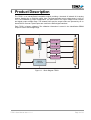
The Embedded I/O Company
TIP551
Optically Isolated
4 Channel 16 Bit D/A
Version 1.1
User Manual
Issue 1.1.4
December 2009
TEWS TECHNOLOGIES GmbH
Am Bahnhof 7 25469 Halstenbek, Germany
Phone: +49 (0) 4101 4058 0 Fax: +49 (0) 4101 4058 19
e-mail: [email protected] www.tews.com
TIP551-10
Optically isolated 4 Channel 16 bit D/A,
0V to +10V or +/-10V Output Voltage Range
This document contains information, which is
proprietary to TEWS TECHNOLOGIES GmbH. Any
reproduction without written permission is forbidden.
TEWS TECHNOLOGIES GmbH has made any
effort to ensure that this manual is accurate and
complete. However TEWS TECHNOLOGIES GmbH
reserves the right to change the product described
in this document at any time without notice.
TEWS TECHNOLOGIES GmbH is not liable for any
damage arising out of the application or use of the
device described herein.
Style Conventions
Hexadecimal characters are specified with prefix 0x,
i.e. 0x029E (that means hexadecimal value 029E).
For signals on hardware products, an ‘Active Low’ is
represented by the signal name with # following, i.e.
IP_RESET#.
©2009 by TEWS TECHNOLOGIES GmbH
All trademarks mentioned are property of their respective owners.
TIP551 User Manual Issue 1.1.4
Page 2 of 16
Issue
Description
Date
Preliminary Issue
August 1997
1.0
First Issue
September 1997
1.1
General Update
July 2002
1.2
New Hardware Version
September 2006
1.3
General Revision
June 2008
1.1.4
New Notation for User Manual and Engineering Documentation
December 2009
TIP551 User Manual Issue 1.1.4
Page 3 of 16
Table of Contents
1
2
PRODUCT DESCRIPTION ......................................................................................... 6
TECHNICAL SPECIFICATION................................................................................... 7
2.1 Analog Output .................................................................................................................................8
2.2 Data Correction ...............................................................................................................................8
2.2.1 DAC Correction Formula for 0V to +10V Output Voltage Range.........................................8
2.2.2 DAC Correction Formula for ±10V Output Voltage Range ..................................................8
3
ID PROM CONTENTS ................................................................................................ 9
3.1 ID PROM Contents TIP551-10 ........................................................................................................9
4
IP ADDRESSING...................................................................................................... 10
4.1
4.2
4.3
4.4
5
Channel Select Register (0x01) ...................................................................................................11
Status Register (0x03) ..................................................................................................................12
Data Register (0x04)......................................................................................................................13
Load Register (0x07).....................................................................................................................13
DAC DATA CODING ................................................................................................ 14
5.1 Bipolar Output Mode.....................................................................................................................14
5.2 Unipolar Output Mode ..................................................................................................................14
6
7
JUMPER CONFIGURATION .................................................................................... 15
IP I/O CONNECTOR................................................................................................. 16
7.1 Analog Output Connections ........................................................................................................16
7.2 Power Input Connections.............................................................................................................16
TIP551 User Manual Issue 1.1.4
Page 4 of 16
List of Figures
FIGURE 1-1 : BLOCK DIAGRAM TIP551 .........................................................................................................6
FIGURE 6-1 : JUMPER CONFIGURATION FOR OUTPUT VOLTAGE RANGE TIP551 ..............................15
List of Tables
TABLE 2-1 : TECHNICAL SPECIFICATION FUNCTIONAL DESCRIPTION...................................................7
TABLE 3-1 : ID PROM CONTENTS TIP551-10................................................................................................9
TABLE 4-1 : ID PROM CONTENTS TIP551-10..............................................................................................10
TABLE 4-2 : CHANSEL DAC CHANNEL SELECT REGISTER .....................................................................11
TABLE 4-3 : STATREG DAC STATUS REGISTER .......................................................................................12
TABLE 4-4 : DATAREG DAC DATA REGISTER............................................................................................13
TABLE 4-5 : LOADREG DAC LOAD REGISTER ...........................................................................................13
TABLE 7-1 : ANALOG OUTPUT CONNECTIONS TIP551.............................................................................16
TABLE 7-2 : POWER INPUT CONNECTIONS TIP551 ..................................................................................16
TIP551 User Manual Issue 1.1.4
Page 5 of 16
1 Product Description
The TIP551 is an IndustryPack® compatible module providing 4 channels of isolated 16 bit analog
outputs. Settling time to 0.003%is typical 10µs. The programmable output voltage range is ±10V or
0 to +10V selectable by jumper configuration. The DAC resets to 0V output voltage in both unipolar
and bipolar output voltage range. The isolated DACs and the output buffers are powered by an on
board DC/DC converter. Optocouplers are used for the DACs digital interfaces.
ID-PROM
16 bit DAC
16 bit DAC
16 bit DAC
16 bit DAC
Industry Pack I/O Interface
Control &
Interface
Optocoupler
Industry Pack logic Interface
Each TIP551 is factory calibrated. The calibration information is stored in the Identification-PROM
unique to each IP and voltage range.
DC/DC
Converter
Figure 1-1 : Block Diagram TIP551
TIP551 User Manual Issue 1.1.4
Page 6 of 16
2 Technical Specification
Logic Interface
IndustryPack® Logic Interface
Size
Single wide IP
I/O Interface
50-conductor flat cable
Analog Outputs
4 D/A channels
Isolation
All D/A channels are galvanically isolated from the IP interface
Output Voltage Range
±10V or 0V to 10V (selectable by jumper), common for all 4
channels
Settling Time of DAC
To 0.003% in 10µs typical
Calibration Data
In ID PROM for gain and offset correction for each channel
Output Current
±4 mA for each channel
Load Capacitance
1nF typical
Accuracy
INL ±4 LSB typical after calibration
Linearity
DNL ±0.5 LSB
Monotonicity
16 bit over the specified temperature range
Wait States
no wait states
Power Requirements
360 mA typical l@+5V with 4mA output current for each channel
Temperature Range
Operating -40°C to +85°C
Storage -45°C to +125°C
MTBF
714000 h
Humidity
5 - 95% non-condensing
Weight
34 g
Table 2-1 : Technical Specification Functional Description
TIP551 User Manual Issue 1.1.4
Page 7 of 16
2.1 Analog Output
The TIP551 includes 4 channels of analog outputs with a resolution of 16 bits and a voltage range of
±10V or 0V to +10V. The maximum output current for each channel is ±4 mA. Each channel has a
settling time to 0.003 % of typical 10 µs.
Two voltage ranges are jumper selectable: ±10V or 0V to +10V. Voltage range selection covers all 4
channels.
The 4 analog outputs of the TIP551 are galvanically isolated from the IndustryPack logic interface by
optocoupler.
2.2 Data Correction
There are two errors which affect the DC accuracy of the DAC. The first is the zero error (offset). For
the DAC this is the data value required to produce a zero voltage output signal. This error is corrected
by subtracting the known error from all readings.
The second error is the gain error. Gain error is the difference between the ideal gain and the actual
gain of the DAC. It is corrected by multiplying the data value by a correction factor.
The data correction values are obtained during factory calibration and are stored in the modules
individual version of the ID PROM. The DAC has a pair of offset and gain correction values for each
single output channel. The correction values are stored in the ID PROM as two’s complement byte
wide values in the range -32768 to 32767. For higher accuracy they are scaled to ¼ LSB.
Because offset and gain correction values are dependent on the selected output voltage range the
TIP551 has 2 different sets of ID PROM data. Depending on the jumper settings for the voltage range
the corresponding set of correction values is automatically selected.
2.2.1 DAC Correction Formula for 0V to +10V Output Voltage
Range
The basic formula for correcting unipolar DAC output value is:
Data = Value * ( 1 - Gaincorr / 262144 ) - Offsetcorr / 4
Data is the (corrected) digital value that should be sent to the DAC, Value is the desired output value,
Gaincorr and Offsetcorr are the correction factors from the ID PROM.
2.2.2 DAC Correction Formula for ±10V Output Voltage Range
The basic formula for correcting bipolar DAC output value is:
Data = Value * ( 1 - Gaincorr / 131072 ) - Offsetcorr / 4
Data is the (corrected) digital value that should be sent to the DAC, Value is the desired output value,
Gaincorr and Offsetcorr are the correction factors from the ID PROM.
Gaincorr and Offsetcorr correction factors are stored separately for each for the four DAC outputs.
Floating point arithmetic or scaled integer arithmetic is necessary to avoid rounding error
while computing above formula.
TIP551 User Manual Issue 1.1.4
Page 8 of 16
3 ID Prom Contents
The Voltage Range bit of the DAC Status Register is used to select the correct set of data correction values for
the actual selected voltage range (transparent for the user).
3.1 ID PROM Contents TIP551-10
ADDRESS
FUNCTION
0x01
ASCII ’I’
Content
0x49
0x03
ASCII ’P’
0x50
0x05
ASCII ’A’
0x41
0x07
ASCII ’C’
0x43
0x09
Manufacturer ID
0xB3
0x0B
Model Number
0x23
0x0D
Revision
0x10
0x0F
reserved
0x00
0x11
Driver-ID low-byte
0x00
0x13
Driver-ID high-byte
0x00
0x15
number of bytes used
0x1D
0x17
CRC
variable
0x19
Version -10
0x0A
0x1B
DAC1 Offset
Ch.1 Low Byte
board dependent
0x1D
DAC1 Offset
Ch.1 High Byte
board dependent
0x1F
DAC2 Offset
Ch.2 Low Byte
board dependent
0x21
DAC2 Offset
Ch.2 High Byte
board dependent
0x23
DAC3 Offset
Ch.3 Low Byte
board dependent
0x25
DAC3 Offset
Ch.3 High Byte
board dependent
0x27
DAC4 Offset
Ch.4 Low Byte
board dependent
0x29
DAC4 Offset
Ch.4 High Byte
board dependent
0x2B
DAC1 Gain
Ch.1 Low Byte
board dependent
0x2D
DAC1 Gain
Ch.1 High Byte
board dependent
0x2F
DAC2 Gain
Ch.2 Low Byte
board dependent
0x31
DAC2 Gain
Ch.2 High Byte
board dependent
0x33
DAC3 Gain
Ch.3 Low Byte
board dependent
0x35
DAC3 Gain
Ch.3 High Byte
board dependent
0x37
DAC4 Gain
Ch.4 Low Byte
board dependent
0x39
DAC4 Gain
Ch.4 High Byte
board dependent
0x3B…0x3F
not used
-
-
Table 3-1 : ID PROM Contents TIP551-10
The TIP551 requires 870us after reset before ID data is ready to be read (ID data is loaded from
serial EEPROM after reset).
TIP551 User Manual Issue 1.1.4
Page 9 of 16
4 IP Addressing
The TIP551 is controlled by a set of registers, which are directly accessible in the I/O address space of
the IP.
All registers are cleared by assertion of IP_RESET#.
Address
Name
Function
Size
0x01
CHANSEL
DAC Channel Select Register
byte
0x03
STATUS
DAC Status Register
byte
0x04
DATAREG
DAC Data Register
word
0x07
LOADDAC
DAC Load Register
byte
0x09
IDWRENA
ID Write Enable Register
byte
Table 4-1 : ID PROM Contents TIP551-10
IDWRENA is for factory use only. Do not write to this register!
TIP551 User Manual Issue 1.1.4
Page 10 of 16
4.1 Channel Select Register (0x01)
The DAC Channel Select Register is used to load conversion data to the DAC internal data register of
a selected DAC channel.
The DAC Data Register must be set up with the conversion data, before the write to the DAC Channel
Select Register is performed.
If Bit 7 is set to '0', the write access to the DAC Channel Select Register does only update the DAC
internal data register of the selected DAC channel. The DAC outputs are not updated in this case.
If Bit 7 is set to '1', the write access to the DAC channel Select Register first updates the DAC internal
data register of the selected channel. After that all 4 DAC outputs are updated according to the DAC
internal data register of each channel.
Write access to the DAC Channel Select Register during active DACBUSY status is ignored and sets
the ERROR flag in the DAC Status Register.
Bit Number
Symbol
Description
7
AL
Automatic Load after Data Transfer
0 = No DAC output update. User can update all
DAC outputs with a write access to the
DAC Load Register or with the next
channel selection write with AL bit set to ‘1’
after data transmission.
1 = All 4 DAC outputs are updated
automatically after data transmission to the
selected DAC channel
6:2
-
1
CS1
Access Reset Value
R/W
0
-
-
R/W
00
Always read as 0
Output Channel Selection
0
CS0
CS1
CS0
Channel
0
0
1
0
1
2
1
0
3
1
1
4
Table 4-2 : CHANSEL DAC Channel Select Register
TIP551 User Manual Issue 1.1.4
Page 11 of 16
4.2 Status Register (0x03)
The DAC Status Register is used to signal status information of the TIP551 which are assisting to
control the conversation of DAC Output.
The DAC Status Register is an 8 bit read only register.
Bit Number
Symbol
7:3
-
2
1
0
ERR
VR
DAC
BUSY
Access
Reset Value
Always read as 0
Description
-
-
Error flag
Write access to the DAC Channel Select
Register or DAC Load Register during active
DACBUSY status is ignored and sets this flag
to ‘1‘. Any write access to the DAC Status
Register clears the ERROR flag.
R
0
Voltage Range flag
Indicates the selected Voltage Range according
to the jumper setting for the output voltage
ranges.
Reading as ’0’ means ±10V output range and
binary two‘s complement as output code
Reading as’1’ means 0V to +10V output range
and straight binary as output code
R
x
DAC Busy flag
Reading as ‘1‘ indicates that a serial data
transfer to the DAC is in progress. Write
access to the DAC Channel Select Register or
DAC Load Register during active DACBUSY
status is ignored and sets the Error flag.
R
0
Table 4-3 : STATREG DAC Status Register
TIP551 User Manual Issue 1.1.4
Page 12 of 16
4.3 Data Register (0x04)
The DAC Data Register contains the DAC conversion data, used by the DAC Channel Select
command.
A write access to the DAC Channel Select Register starts the serial data transfer to the DAC (and if
selected the conversion into an analog value).
Immediately after a write to the DAC Channel Select register, the DAC Data Register may be written
with the next conversion data value. However, before the next write to the DAC Channel Select
Register, the DACBUSY status bit must be '0'.
The content of the DAC Data Register is valid until it is re-written by the user.
The DAC Data Register does not need to be updated if the DAC conversion data value for the next
DAC Channel Select command should be the same.
Bit Number
Symbol
15:0
-
Description
This register contains the desired DAC
conversion data value used by the DAC
Channel Select command.
Access
Reset Value
R/W
0x0000
Table 4-4 : DATAREG DAC Data Register
For data coding see chapter “DAC Data Coding”.
4.4 Load Register (0x07)
Every write access to the DAC Load Register updates all 4 DAC outputs with the last value written into
the DACs internal data register.
Write access to the DAC Load Register during active DACBUSY status is ignored and sets the
ERROR flag in the DAC Status Register.
Bit Number
7:0
Symbol
Description
-
Write access updates all 4 DAC outputs with
the conversion data stored in the DACs internal
data register.
DACBUSY status must be '0' before are write
to the DAC Load Register.
Access Reset Value
W
-
Table 4-5 : LOADREG DAC Load Register
TIP551 User Manual Issue 1.1.4
Page 13 of 16
5 DAC Data Coding
5.1 Bipolar Output Mode
If the DAC channels are configured for ±10V output voltage range by the corresponding jumper
configuration the following DAC data coding applies:
DATAREG
OUTPUT
0x7FFF
+ Full-scale
0x8000
- Full-scale
0x0000
Midscale
5.2 Unipolar Output Mode
If the DAC channels are configured for 0V to +10V output voltage range by the corresponding jumper
configuration the following DAC data coding applies:
TIP551 User Manual Issue 1.1.4
DATAREG
OUTPUT
0xFFFF
+ Full-scale
0x8000
Midscale
0x0000
Zero-scale
Page 14 of 16
6 Jumper Configuration
On the TIP551 the desired DAC output voltage range is configured by a 3 pin jumper field.
The configured DAC output voltage range applies to all four DAC channels.
Jumper Configuration :
Voltage range 0V to +10V :
J1 1-2 installed
Voltage range ±10V :
J1 2-3 installed
J1
3
2
Industry Pack I/O Interface
Industry Pack logic Interface
1
Figure 6-1 : Jumper Configuration for Output Voltage Range TIP551
Factory configuration is 0V to +10V output voltage range for all DAC channels.
TIP551 User Manual Issue 1.1.4
Page 15 of 16
7 IP I/O connector
7.1 Analog Output Connections
Pin-Number
Signal
01
DAC_OUT1
02
AGND
03
DAC_OUT2
04
AGND
05
DAC_OUT3
06
AGND
07
DAC_OUT4
08
AGND
Table 7-1 : Analog Output Connections TIP551
7.2 Power Input Connections
Pin-Number
Function
44
AGND
45
-15V
46
AGND
47
+15V
48
AGND
49
+5V
50
AGND
Table 7-2 : Power Input Connections TIP551
The power input connections are reserved for special versions of the TIP551 without on board
DC/DC converter. Do not supply any voltage to these pins for the TIP551-10 version.
TIP551 User Manual Issue 1.1.4
Page 16 of 16