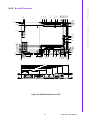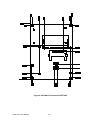
1
User Manual
PCM-4372
Onboard VIA Eden™ EPIC CPU
Module
Copyright
The documentation and the software included with this product are copyrighted
2007 by Advantech Co., Ltd. All rights are reserved. Advantech Co., Ltd. reserves
the right to make improvements in the products described in this manual at any
time without notice. No part of this manual may be reproduced, copied, translated
or transmitted in any form or by any means without the prior written permission of
Advantech Co., Ltd. Information provided in this manual is intended to be
accurate and reliable. However, Advantech Co., Ltd. assumes no responsibility
for its use, nor for any infringements of the rights of third parties, which may result
from its use.
This document is copyrighted, 2007. All rights are reserved. The original
manufacturer reserves the right to make improvements to the products described
in this manual at any time without notice. No part of this manual may be
reproduced, copied, translated or transmitted in any form or by any means
without the prior written permission of the original manufacturer. Information
provided in this manual is intended to be accurate and reliable. However, the
original manufacturer assumes no responsibility for its use, nor for any
infringements upon the rights of third parties that may result from such use.
Acknowledgements
Award is a trademark of Award Software International, Inc.
VIA is a trademark of VIA Technologies, Inc.
IBM, PC/AT, PS/2 and VGA are trademarks of International Business Machines
Corporation.
Intel and Pentium are trademarks of Intel Corporation.
Microsoft Windows is a registered trademark of Microsoft Corp.
RTL is a trademark of Realtek Semi-Conductor Co., Ltd.
ESS is a trademark of ESS Technology, Inc.
UMC is a trademark of United Microelectronics Corporation.
SMI is a trademark of Silicon Motion, Inc.
Creative is a trademark of Creative Technology LTD.
CHRONTEL is a trademark of Chrontel Inc.
All other product names or trademarks are properties of their respective owners.
PCM-4372 User Manual
Part No. 2006437211
Edition 2
Printed in Taiwan
June 2007
ii
Product Warranty
Warranty Period
ADVANTECH aims to meet the customer's expectations for post-sales service
and support; therefore, in addition to offering 2 years global warranty for
ADVANTECH's standard products, a global extended warranty service is also
provided for customers upon request. ADVANTECH customers are entitled to a
complete and prompt repair service beyond the standard 2 years of warranty.
Standard products manufactured by ADVANTECH are covered by a 2 year's
global warranty from the date of shipment. Products covered by extended
warranty and cross-region repair services against defects in design, materials,
and workmanship, are also covered from the date of shipment. All of key parts
assembled into ADVANTECH system products such as LCD, Touch Screen,
Power Supply, and peripherals etc, will be also covered by the standard 2 years
of warranty.
Repairs under Warranty
It is possible to obtain a replacement (cross-shipment) during the first 30 days of
the purchase (45 days for Channel Partners), if the products were purchased
directly from ADVANTECH and the product is DOA (Dead-on-Arrival). DOA
cross-shipment excludes any customized and/or build-to-order products. The
cross-shipment agreement signed by customers is required for initiating/releasing
cross shipment with ADVANTECH confirmation and verification. The only
conditions for cross-shipment are: a) the return must not be damaged, altered or
marked, b) all parts and accessories must be included as originally shipped; and
c) proof of purchase must be included. Any returns that do not meet mentioned
requirements above, or any wrong user settings/configurations will be denied, or
subject to additional handling/service charges as determined by the
ADVANTECH Repair Service Department. For those products which are not
DOA, the return fee to an authorized ADVANTECH repair facility will be at the
customers' expense. The shipping fee for reconstructive products from
ADVANTECH back to customers' sites will be at ADVANTECH's expense.
iii
PCM-4372 User Manual
Exclusions from Warranty
The product is excluded from warranty if:
•
The product has been found to be defective after expiry of the warranty
period.
•
Warranty has been voided by removal or alternation of product or part identification labels.
•
The product has been misused, abused, or subjected to unauthorized disassembly/modification; placed in an unsuitable physical or operating environment; improperly maintained by the customer; or failure caused which
ADVANTECH is not responsible whether by accident or other cause. Such
conditions will be determined by ADVANTECH at its sole unfettered discretion.
•
The product is damaged beyond repair due to a natural disaster such as a
lighting strike, flood, earthquake, etc.
•
Product updates/upgrades and tests upon the request of customers who are
without warranty.
Technical Support and Assistance
For more information about this and other Advantech products, please visit our
website at:
http://www.advantech.com/
http://www.advantech.com/ePlatform/
For technical support and service, please visit our support website at:
http://support.advantech.com.tw/support/
Additional Information and Assistance
1. Visit the Advantech web site at http://www.advantech.com/ where you can
find the latest information about the product.
2. Contact your distributor, sales representative, or Advantech's customer service center for technical support if you need additional assistance. Please
have the following information ready before you call:
•
Product name and serial number
•
Description of your peripheral attachments
•
Description of your software (operating system, version, application software, etc.)
•
A complete description of the problem
•
The exact wording of any error messages
PCM-4372 User Manual
iv
Declaration of Conformity
CE
This product has passed the CE test for environmental specifications. Test
conditions for passing included the equipment being operated within an industrial
enclosure. In order to protect the product from being damaged by ESD
(Electrostatic Discharge) and EMI leakage, we strongly recommend the use of
CE-compliant industrial enclosure products.
FCC Class A
This device complies with the requirements in part 15 of the FCC rules: Operation
is subject to the following two conditions:
1.This device may not cause harmful interference, and
2. This device must accept any interference received, including interference that
may cause undesired operation
This equipment has been tested and found to comply with the limits for a Class A
digital device, pursuant to Part 15 of the FCC Rules. These limits are designed to
provide reasonable protection against harmful interference when the equipment
is operated in a commercial environment. This equipment generates, uses, and
can radiate radio frequency energy and, if not installed and used in accordance
with the instruction manual, may cause harmful interference to radio
communications.
Operation of this device in a residential area is likely to cause harmful
interference in which case the user will be required to correct the interference at
his/her own
expense. The user is advised that any equipment changes or modifications not
expressly approved by the party responsible for compliance would void the
compliance to FCC regulations and therefore, the user's authority to operate the
equipment.
FM
This equipment has passed the FM certification. According to the National Fire
Protection Association, work sites are classified into different classes, divisions
and groups, based on hazard considerations. This equipment is compliant with
the specifications of Class I, Division 2, Groups A, B, C and D indoor hazards.
Document Feedback
To assist us in making improvements to this manual, we would welcome
comments and constructive criticism. Please send all such - in writing to:
[email protected]
v
PCM-4372 User Manual
Packing List
Before setting up the system, check that the items listed below are included and
in good condition. If any item does not accord with the table, please contact your
dealer immediately.
Item
Part Number
1 PCM-4372 SBC
1 Startup manual
1 Utility CD
1 mini jumper pack
9689000002
FLAT Cable 50P 20CM 3Com & LPT 1.27mm
to D-sub
1700002034
FLAT Cable 44P IDC 44P/44P/40P keyed
50CM
1701440504
Cable 20P/10P 10CM EPIC ATX Power
1700002055
Cable 6pin, 6-pin; 20CM long: PS/2 KB &
Mouse
1700060202
USB CABLE 20 Pin TO 2 Port, L=30 cm PCM43xx series
1700004891
CABLE Serial ATA 7P/7P 100cm
1700071000
Wire RS-422/485 W/D-SUB COM 4P 15cm
1703040157
Ordering Information
Model Number Description
PCM-4372F-S0A1E Eden ULV 1.0GHz w/CF/VGA/LCD/LVDS/SATA
PCM-4372U-S0A1E Eden ULV 1.0GHz w/USB-DOM/VGA/LCD/LVDS/SATA
PCM-4372F-M0A1E Eden 600MHz w/CF/VGA/LCD/LVDS/SATA
PCM-4372F-J0A1E Eden 400MHz w/CF/VGA/LCD/LVDS/SATA
Optional accessories
Model Number Description
PCD-USBH1I-MS0256 USB-DOM, 256 MB, -40 ~ 85 ° C
PCD-USBH1I-MS0512 USB-DOM, 512 MB, -40 ~ 85 ° C
PCD-USBH1I-MS1024 USB-DOM, 1 GB, -40 ~ 85 ° C
PCD-USBH1I-MS2048 USB-DOM, 2 GB, -40 ~ 85 ° C
PCM-410B-00A1E HD Audio/USB module for EPIC
PCM-410-00A1E Audio/USB/COM/LPT daughter board for EPIC
PCM-4372 User Manual
vi
Safety Instructions
1.
2.
3.
4.
5.
6.
7.
8.
9.
10.
11.
12.
13.
14.
15.
16.
17.
18.
19.
20.
Read these safety instructions carefully.
Keep this User Manual for later reference.
Disconnect this equipment from any AC outlet before cleaning. Use a damp cloth.
Do not use liquid or spray detergents for cleaning.
For plug-in equipment, the power outlet socket must be located near the equipment
and must be easily accessible.
Keep this equipment away from humidity.
Put this equipment on a reliable surface during installation. Dropping it or letting it
fall may cause damage.
The openings on the enclosure are for air convection. Protect the equipment from
overheating. DO NOT COVER THE OPENINGS.
Make sure the voltage of the power source is correct before connecting the
equipment to the power outlet.
Position the power cord so that people cannot step on it. Do not place anything over
the power cord.
All cautions and warnings on the equipment should be noted.
If the equipment is not used for a long time, disconnect it from the power source to
avoid damage by transient overvoltage.
Never pour any liquid into an opening. This may cause fire or electrical shock.
Never open the equipment. For safety reasons, the equipment should be opened
only by qualified service personnel.
If one of the following situations arises, get the equipment checked by service
personnel:
The power cord or plug is damaged.
Liquid has penetrated into the equipment.
The equipment has been exposed to moisture.
The equipment does not work well, or you cannot get it to work according to the
user's manual.
The equipment has been dropped and damaged.
The equipment has obvious signs of breakage.
Chapter
1
General Information ............................1
1.1
1.2
General Information .................................................................................. 2
Product Features....................................................................................... 2
1.2.1 General ......................................................................................... 2
1.2.2 Display .......................................................................................... 2
Specifications ............................................................................................ 3
1.3.1 Processor: VIA Eden CPU: ........................................................... 3
1.3.2 Chipset: VIA CX700 chipset:......................................................... 3
1.3.3 Other Functions ............................................................................ 5
1.3.4 Mechanical Specification .............................................................. 6
1.3.5 Power Supply Voltage................................................................... 6
1.3.6 Power Supply Current................................................................... 6
Table 1.1: CPU : Eden ULV 1.0 GHz , RAM:533 MHz 1 GB DDR2
SDRAM....................................................................... 6
Table 1.2: CPU : Eden ULV 1.0 GHz , RAM:533 MHz 1 GB DDR2
SDRAM....................................................................... 6
1.3.7 RTC Battery .................................................................................. 7
1.3.8 Environmental Specification.......................................................... 7
1.3
Chapter
2
H/W Installation....................................9
2.1
2.2
H/W Installation ....................................................................................... 10
Jumpers .................................................................................................. 10
2.2.1 Jumper List ................................................................................. 10
Table 2.1: J1.............................................................................. 10
Table 2.2: J2.............................................................................. 10
Table 2.3: J3.............................................................................. 10
Table 2.4: J4.............................................................................. 10
Table 2.5: J5.............................................................................. 10
2.2.2 Jumper Description ..................................................................... 11
Table 2.6: PCI VIO Setting (J5) ................................................. 11
Connector Settings.................................................................................. 12
2.3.1 Connectors List ........................................................................... 12
2.3.2 GPIO (General Purpose Input Output) (CN2) ............................. 12
2.3.3 COM Port Connector (CN4, CN5, CN6) ..................................... 12
2.3.4 Parallel Port Connector (CN5) .................................................... 13
2.3.5 Power Connectors (CN5, CN26)................................................. 13
2.3.6 Fan Power Supply Connector (CN7) .......................................... 13
2.3.7 Keyboard and PS/2 Mouse Connector (CN8)............................. 13
2.3.8 IDE, CDROM Hard Drive Connector (CN9) ................................ 13
2.3.9 Solid State Disk: CompactFlash (CN10)..................................... 14
2.3.10 Power & HDD LED Connector (CN11) ....................................... 14
2.3.11 Power Reset Button (S1) ............................................................ 14
2.3.12 VGA/LCD/LVDS Interface Connections (CN13, CN14, CN21)... 14
2.3.13 Ethernet Configuration (CN15, CN16) ........................................ 14
2.3.14 USB Connectors (CN17, CN18, CN27) ...................................... 14
2.3.15 SATA Connector (SA1, SA2) ...................................................... 14
Mechanical .............................................................................................. 15
2.4.1 Jumper & Connector Location .................................................... 15
Figure 2.1 PCM-4372 Position TOP .......................................... 15
Figure 2.2 PCM-4372 Position BOTTOM .................................. 16
2.4.2 Board Dimension ........................................................................ 17
Figure 2.3 PCM-4372 Dimension TOP ...................................... 17
Figure 2.4 PCM-4372 Dimension BOTTOM .............................. 18
2.3
2.4
Chapter
3
BIOS Settings.....................................21
ix
PCM-4372 User Manual
Chapter
Chapter
3.1
3.2
BIOS Operation....................................................................................... 22
BIOS Setup ............................................................................................. 22
3.2.1 Main Menu .................................................................................. 23
3.2.2 Standard CMOS Features .......................................................... 24
3.2.3 Advanced BIOS Features ........................................................... 25
3.2.4 Advanced Chipset Features ....................................................... 27
3.2.5 Integrated Peripherals ................................................................ 28
3.2.6 Power Management Setup ......................................................... 29
3.2.7 PnP/PCI Configurations.............................................................. 31
3.2.8 PC Health Status ........................................................................ 32
3.2.9 Frequency/voltage Control.......................................................... 33
3.2.10 Load Optimized Defaults ............................................................ 33
3.2.11 Set Password.............................................................................. 34
3.2.12 Save & Exit Setup....................................................................... 35
3.2.13 Quit Without Saving .................................................................... 36
4
S/W Installation ................................. 37
4.1
4.2
4.3
S/W Installation ....................................................................................... 38
Driver Installation .................................................................................... 38
SUSI Application Library ......................................................................... 38
4.3.1 SUSI Introduction........................................................................ 38
4.3.2 SUSI Functions........................................................................... 38
4.3.3 SUSI Sample Programs.............................................................. 41
5
5.1
Installing Extension
I/O ................. 47
5.2
5.3
5.4
5.5
MIO Introduction ..................................................................................... 48
5.1.1 M2M Concept ............................................................................. 48
5.1.2 Easy Wireless Technology For Your Embedded Motherboard... 48
5.1.3 Best Board Combination............................................................. 48
Figure 5.1 PCM-4372 + MIO 2320 ............................................ 48
PC/104 Module Introduction ................................................................... 49
MIO-USB Introduction............................................................................. 50
Installing SO-DIMM................................................................................. 51
Optional Modules .................................................................................... 51
5.5.1 MIO-2310 Wireless Module ........................................................ 51
5.5.2 MIO-2320 GSM/GPRS Module................................................... 51
5.5.3 MIO-3121 Mini-PCI to 4 COMs Module ...................................... 52
5.5.4 MIO-3140 Mini-PCI to 2 SATA Module....................................... 52
5.5.5 MIO-3150 Mini-PCI to Video Capture Module ............................ 52
Appendix A
PIN Assignments .............................. 53
A.1
PIN Assignements .................................................................................. 54
Table A.1: GPIO Connector (CN2) ............................................ 54
Table A.2: Power Switch (CN3) ................................................. 54
Table A.3: COM1 (CN4) ............................................................ 54
Table A.4: CN5 COM2/3/4 & LPT.............................................. 55
Table A.5: RS-422/485 (CN6).................................................... 57
Table A.6: System FAN (CN7)................................................... 57
Table A.7: KB_MS (CN8)........................................................... 58
Table A.8: IDE0 (CN9)............................................................... 58
Table A.9: Compact II W/Ejector (CN10)................................... 59
Table A.10:HD & Power LED (CN11) ......................................... 61
Table A.11:Inverter Power (CN12) ............................................. 61
Table A.12:LVDS0 Connector (CN13)........................................ 62
Table A.13:VGA Connector (CN14)............................................ 63
PCM-4372 User Manual
x
Table A.14:LAN1 (RJ45+100M Transformer)( CN15) ................ 63
Table A.15:LAN2 (RJ45+100M Transformer) (CN16) ................ 64
Table A.16:USB0/1 (CN17)......................................................... 64
Table A.17:USB2/3 & AC97 (AUDIO I/F) (CN18) ....................... 65
Table A.18:USB4/5(MIO-USB) (CN19)....................................... 65
Table A.19:Inverter Power (CN20).............................................. 66
Table A.20:LVDS1 Connector (CN21) ........................................ 66
Table A.21:ISA_-5V (CN24)........................................................ 68
Table A.22:ATX Power Connector (CN26) ................................. 68
Table A.23:USB4/5 (CN27)......................................................... 69
Appendix B
System Assignments ........................71
B.1
B.2
System Assignments............................................................................... 72
System I/O Ports ..................................................................................... 72
Table B.1: System I/O ports....................................................... 72
1st MB memory map ............................................................................... 72
Table B.2: Table C.2: 1st MB memory map............................... 72
DMA channel assignments ..................................................................... 73
Table B.3: DMA channel assignments....................................... 73
Interrupt assignments.............................................................................. 73
Table B.4: Interrupt assignments ............................................... 73
B.3
B.4
B.5
Chapter
1
1
General Information
This chapter gives background
information on the PCM-4372
Sections include:
! Introduction
! Features
! Specifications
1.1 General Information
PCM-4372 is an EPIC SBC (Single Board Computer) with high performance and
lower power based on VIA Eden processors. The PCM-4372, in conjunction with VIA
CX700 chipset, supports processors clocked at up to 1GHz, six USB 2.0 compatible
ports, dual 10/100Base-T Ethernet interface, 2 Channel LVDS interface, and one
MIO expansion connector (CF or USB-DOM), and can accommodate up to 1GB of
ECC DDR RAM memory. The PCM-4372 also supports two SATA and four COM
ports.
1.2 Product Features
1.2.1 General
!
!
!
!
!
!
!
!
!
!
!
!
!
!
!
!
!
!
!
CPU Embedded VIA Eden processor
System Chipset VIA CX700
BIOS AWARD 4 Mbit Flash BIOS
System Memory 200-pin SODIMM socket, support ECC Double Data Rate
(DDR2) 128 MB to 1 GB, accept 128/256/512/1 GB DDR 400/533 DRAM
Power Management APM1.2, ACPI support
SSD Supports CompactFlash Card TYPE I/II (shared 1st IDE Channel) USB
memory, uDOC (Optional)
Watchdog Timer Single chip Watchdog 255-level interval timer, setup by software
Expansion Interface Supports 8/16 bit ISA bus for standard PC/104 device
(ITE 8888g), PC/104-Plus
Battery 2-pin wafer box for external Battery on board I/O
I/O Interface 1 x EIDE (UDMA 33), 1 x K/B, 1 x KB/mouse, 3 x RS232, 1 x
RS232/422/485, 1 x LPT
USB 6 x USB 2.0 compliant Ports (2 ports on board connector, 4 ports pinhead)
Audio CX700 HD 3D surround stereo sound Supports Line -in, Line-out, Microphone-in (with PCM-410 option)
IrDA N/A
GPIO 8-bit general purpose input/output Ethernet
Chipset Intel 82551, 82541PI (Gigabit for optional)
Speed 10/100 Mbps
Interface 2 x RJ45
Standard IEEE 802.3u 100Base-T
1.2.2 Display
!
!
!
!
!
!
!
!
Chipset VIA CX700 chip integrated. (Extreme Graphics 2)
Memory Size Optimized Shared Memory Architecture, supports up to 64 MB
frame buffer using system memory
Resolution CRT Display mode: pixel resolution up to 1600 x 1200 at 85-Hz and
2048 x 1536 at 75-Hz LCD Display mode: Dual channel LVDS panel supports
up to UXGA panel resolution with frequency range from 25 MHz to 112 MHz
LCD Interface 2 Channel
1 x 24/48-bit LVDS
1 x 24/48-bit LVDS
LVDS Two Hirose connectors support up to 2 channel LVDS LCD Panel
Dual Independent CRT + LVDS, LVDS + LVDS (optional)
PCM-4372 User Manual
2
Chapter 1
1.3 Specifications
1.3.1 Processor: VIA Eden CPU:
• Supports 400 MHz FSB VIA Eden CPU.
• Supports 400M / 600M / ULV1.0GHz CPU.
21mm *21mm Flip Chip Nano-BGA2.
1.3.2 Chipset: VIA CX700 chipset:
3
PCM-4372 User Manual
General Information
Memory:
DDR2 533/400 SDRAM.
Maximum 1GB DDR2 SDRAM.
Socket:
1 x 200 pin SO-DIMM socket type *1
Graphic and Video Controllers : VIA CX700 chipset supports:
DuoView+ Capability
• Dual displays: CRT+LVDS1, LVDS1+LVDS2. (These use different
BIOS.)
• WinXP, Extended desktop support.
LVDS1 Panel Display Interface
• Compatible with TIA/EIA-644.
• Supports panel resolution from VGA through UXGA (1600 x 1200)
• Supports 1 x Dual-Channel LVDS panel.
LVDS connector : Hirose DF13 type 40 pin
CRT
• CRT display interface with 30-bit true-color RAMDAC up to 350
MHz pixel rate with gamma correction capability.
• Supports CRT resolutions up to 2048x1536.
Analog CRT Connector : D-sub 15-pin 5mm (Black)
IDE Interface: VIA CX700 chip supports:
• Single channel EIDE controller supporting 2 Enhanced IDE devices.
• Data transfer rate up to 33MB/sec to cover PIO mode 4, Multi-word
DMA mode 2, and UltraDMA-33 interface.
• Supports ATPAI compliant devices including DVD devices.
• Supports PCI native and ATA compatibility modes.
IDE Primary Connector:
• 40pin 2.54 mm Box Header
SSD:
Option 1: VIA CX700 chip supports:
IDE Interface Master Mode default.
• Supports Compact Flash Card Type I.
Socket:
• 50 pin Compact Flash Card Type I connector.
Option 2: VIA CX700 chip supports:
• uDOC (uDiskONChip from M-Systems) socket on board, occupying
USB 2.0 port no. 5
HD Audio Link: VIA CX700 controller chip supports:
• High performance audio controller with 192KHz sample rate, 32-bit
per sample and up to 8 channels.
• Line-in, Line-out, Mic-in (Mono), CD-in, Side-Surround, Back-Surround, Center-out, Bass out.
Connectors:
• HD Link : Pin header 8*2P (M) 2.0mm
Module:
• PCM-410.
PC/104-plus expansion:
PCI-104: VIA CX700 chip supports.
• PCI 2.2 compliant.
• 32-bit 3.3V 33MHz PCI interface with 5V tolerant inputs.
• Supports PC/PCI DMA
PCI Socket:
• 30*4(F) 2.00mm PC/104+ Solder 63.35mm*7.87mm*9.35mm.
PC104: ITE8888G supports:
• Supports full ISA compatible functions
• Supports ISA at 1/4 of PCI frequency
PC104 Socket:
Socket2. 20*2(F) 2.54mm 51.86mm*5.01mm*11.45mm p=3.40mm
Socket3. 32*2(F) 2.54mm 82.34mm*5.01mm*11.45mm p=3.40mm
SATA Connector: VIA CX700 chip supports:
• Supports up to 2 SATA devices.
• Supports 1.5Gbit/s transfer rate.
• Complies with SATA specification rev.1.0.
SATA connectors.
• Serial ATA 7pins 1.27mm*2
USB Interface: VIA CX700 chip supports:
• Six USB 2.0 ports.
• Legacy keyboard and PS/2 mouse support.
USB Connector:
• (USB1~2) 2 USB connector on front site.
• (USB3~4) Audio pin header.
Module:
• PCM-410.
• (USB5~6) 2 set 5x2pin 2.0mm pin header (USB5: supports Advantech MIO-USB type flash Standard Specification.)
Power Management: VIA CX700 chip supports:
• Supports both ACPI (Advanced Configuration and Power Interface)
2.0 and legacy APM V1.2 power management.
BIOS : VIA CX700 chip supports:
• Phoenix 4M bit Flash BIOS, supports Plug & Play, APM 1.2/ACPI
1.1.
• FWH Type.
Socket:
• 32 pin PLCC socket
PCM-4372 User Manual
4
5
PCM-4372 User Manual
General Information
Graphic and Video Controllers
LVDS2 Interface
LVDS Transmitter chip:VIA VT1636 supports.
• Double-data-rate data transfer with clock rates up to 165MHz
• Supports panel resolution from VGA through UXGA (1600x1200)
• Supports 1 x Dual-Channel LVDS panel
LVDS connector : Hirose DF13 type 40 pin
Serial Ports: Winbond W83627HF (LPC Super I/O) and Fintek F81216DG supports.
• 2 full function serial ports by Winbond W83627
• 2 full function serial ports by Fintek F81216DG
• High Speed NS16C550A Compatible UARTs with Data rates to
1.5Mbps
• Supports IRQ Sharing among serial ports
Connectors:
• COM1: (RS-232) 1x DB9 on front site
• COM2: (RS-232/422/485) 1 x 1.27mm box header
• COM3~4: (RS-232) 1 x 1.27mm box header
• Module:PCM-410
Thermal Sensor: WinbondW 83627HF (LPC Super I/O) supports.
Parallel Port: Winbond W83627HF (LPC Super I/O) supports.
• One Parallel Port
• SPP/EPP (1.7,1.9)/ECP (IEEE 1284 Compliant) mode
Connector:
• Box header 15*2P (M) 1.27mm
• Module:PCM-410
Keyboard/Mouse Connector: Winbond W83627HF supports.
• PS/2 Keyboard and Mouse interface
Connector: Mini-Din 6P On Front Site
LAN: Intel 82551 supports.
• 82551: Integrated IEEE 802.3 10BASE-T and 100BASE-TX compatible PHY
• Two LAN chips
Connectors:
• Phone Jack RJ45 8P 90D(F)*2
GPIO: PCA9554 supports.
• SMbus expansion
• 8 I/O Pins
• 5V tolerance I/Os
Connectors:
• Connector: 10 pins 2.0mm pin header
Fan:
Connector:
• 3 pins 2.0mm Wafer box
Battery Backup:
• 2 pin wafer box for external Battery on board
Chapter 1
1.3.3 Other Functions
1.3.4 Mechanical Specification
Dimension (mm)
• L 164 mm x W115 mm
Height on Top (mm)
• 27.6 mm (Heatsink)
Height on Bottom (mm)
• 7.5 mm (CN10)
Heatsink Dimension (mm)
• L 109 mm x W 52 mm x H 27.6 mm
Weight(g) with Heatsink
• 340g
1.3.5 Power Supply Voltage
Voltage requirement with ATX Power:
+5 V DC +/-5%
+5 V DC Standby +/- 5%
+3.3 V DC +/-5%
+12 V DC (For DDR PWM Power enable, some PC/104, PC/104+
cards and two LVDS inverter power)
-12 V DC (For some PC/104, PC/104+ cards)
Voltage requirement with AT Power:
+5 V DC +/-5%
+12 V DC (For DDR PWM Power enable, some PC/104, PC/104+
cards and two LVDS inverter power)
1.3.6 Power Supply Current
Supply Current (Typical)
Table 1.1: CPU : Eden ULV 1.0 GHz , RAM:533 MHz 1 GB DDR2
SDRAM
Dos
BIOS
WINXP Idle
WINXP HCT11.0
WINXP 3DMARK2001SE
ATX
5V
1.91A
1.91A
1.59A
2.05A
2.21A
12V
0.12A
0.09A
0.09A
0.12A
0.12A
3.3V
0.53A
0.52A
0.53A
0.54A
0.53A
5V Standby
0.30A
0.31A
0.28A
0.37A
0.49A
5V
2.42A
2.42A
2.06A
2.69A
3.25A
12V
0.12A
0.12A
0.12A
0.14A
0.11A
Supply Current (Maximum)
Table 1.2: CPU : Eden ULV 1.0 GHz , RAM:533 MHz 1 GB DDR2
SDRAM
ATX
5V
AT
12V
3.3V
5V Standby 5V
Eden ULV 1.0 GHz + 533 MHz 1.0 GB 2.21A 0.12A 0.54A 0.49A
DDR2 SDRAM
PCM-4372 User Manual
6
3.25
A
12V
0.14
A
Typical Voltage : 3.0V
Normal discharge capacity : 210mAh
1.3.8 Environmental Specification
Operating Temperature
The VIA EDEN is specified for proper operation when the junction
temperature is within the specified range of 0° C to 100° C.
Operating temperature: 0 ~ 60° C (32~140° F)
Operating Humidity
Operating Humidity: 0% ~ 90% Relative Humidity, non-condensing
Storage Temperature
Standard products (0~60° C)
Storage temperature: -20~70° C
Phoenix products (-20~80° C)
Storage temperature: -20~80° C
Platinum Phoenix products (-40~85° C)
Storage temperature: -40~85° C
Storage Humidity
Standard products (0~60° C)
Relative Humidity: 95% @ 60° C
Phoenix products (-20~80° C)
Relative Humidity: 95% @ 60° C
Platinum Phoenix products (-40~85° C)
Relative Humidity: 95% @ 60° C
7
PCM-4372 User Manual
General Information
The VIA CX700 chipset operating temperature runs at a maximum of
85° C.
Chapter 1
1.3.7 RTC Battery
Chapter
2
2
H/W Installation
This chapter explains the setup
procedures of the PCM-4372 hardware, including instructions on
setting jumpers and connecting
peripherals, switches, indicators
and mechanical drawings. Be sure
to read all safety precautions
before you begin the installation
procedure.
2.1 H/W Installation
2.2 Jumpers
This chapter explains the setup procedures of PCM-4372 hardware, including
instructions on setting jumpers and connecting peripherals, switches, indicators and
mechanical drawings. Be sure to read all safety precautions before you begin the
installation procedure.
2.2.1 Jumper List
J1
J2
J3
J4
J5
Clear CMOS
COM2 Setting
LVDS0 Power
LVDS1 Power
PCI VIO Setting
Table 2.1: J1
J1
Clear CMOS
Setting
Function
(1-2)
Normal
(2-3)
Clear CMOS
Table 2.2: J2
J2
COM2 Setting
Setting
Function
(1-2)
RS232
(3-4)
RS485
(5-6)
RS422
Table 2.3: J3
J3
LVDS0 Power
Setting
Function
(1-2)
+5 V
(2-3)
+3.3 V
Table 2.4: J4
J4
LVDS1 Power
Setting
Function
(1-2)
+5 V
(2-3)
+3.3 V
Table 2.5: J5
J5
PCI VIO Setting
Setting
Function
(1-2)
+5 V
(2-3)
+3.3 V
PCM-4372 User Manual
10
You can configure your card to match the needs of your application by setting jumpers. A jumper is a metal bridge used to close an electric circuit. It consists of two
metal pins and a small metal clip (often protected by a plastic cover) that slides over
the pins to connect them. To close a jumper you connect the pins with the clip. To
open a jumper you remove the clip. Sometimes a jumper will have three pins, labeled
1, 2 and 3. In this case you would connect either pins 1 and 2, or 2 and 3.
closed
closed 2-3
The jumper settings are schematically depicted in this manual as follows:
closed
open
closed 2-3
A pair of needle-nose pliers may be helpful when working with jumpers. If you have
any doubts about the best hardware configuration for your application, contact your
local distributor or sales representative before you make any changes. Generally,
you simply need a standard cable to make most connections.
Table 2.6: PCI VIO Setting (J5)
Setting
Function
1-2
+5V
2-3
+3.3V
Warning! To avoid damaging the computer, always turn off the power supply before
setting.Clear CMOS. Before turning on the power supply, set the jumper back
to 3.0 V Battery On.
11
PCM-4372 User Manual
H/W Installation
open
Chapter 2
2.2.2 Jumper Description
2.3 Connector Settings
2.3.1 Connectors List
CN1 Battery Con.
CN2 GPIO
CN3 Power Switch
CN4 COM1
CN5 COM2/3/4 & LPT
CN6 RS-422/485
CN7 System FAN
CN8 KB_MS
CN9 IDE0
CN10 Compack II W/O Ejector
CN11 HD & Power LED
CN12 Inverter Power0
CN13 LVDS0 Connector
CN14 VGA Connector
CN15 LAN1(RJ45)
CN16 LAN2(RJ45)
CN17 USB0/1
CN18 USB2/3 & AC97 (AUDIO I/F)
CN19 USB4/5(MIO-USB)
CN20 Inverter Power1
CN21 LVDS1 Connector
CN23 PC104/+
CN24 ISA_-5V
CN26 ATX Power Con.
CN27 USB4/5
DIMM1 DDR-SODIMM(RVS)-5.2mm
SA1 SATA1
SA2 SATA2
2.3.2 GPIO (General Purpose Input Output) (CN2)
The board supports 8-bit GPIO via a GPIO connector. The 8 digital in/out-puts can be
programmed to read or control devices, with input or out- puts defined. The default
setting is 4 bits input and 4 bits output.
2.3.3 COM Port Connector (CN4, CN5, CN6)
PCM-4372 provides 4 serial ports (COM1: RS-232; COM2: RS-232/422/485) in one
DB-9 connector (COM1) and one 50-pin dual-inline, male header. It provides connections for serial devices (mouse, etc.) or a communication network. You can find the
pin assignments for the COM port connector in Appendix A.
PCM-4372 User Manual
12
2.3.5 Power Connectors (CN5, CN26)
Main power connector, +3.3V, +5 V, +12 V (CN26).
Supplies main power to the PCM-4372 (+5 V), and to devices that require +12 V.
2.3.6 Fan Power Supply Connector (CN7)
Provides +5 V power supply to the CPU cooling fan.
2.3.7 Keyboard and PS/2 Mouse Connector (CN8)
The board provides a keyboard connector that supports both a keyboard and a PS/2
style mouse. In most cases, especially in embedded applications, a keyboard is not
used. If the keyboard is not present, the standard PC/AT BIOS will report an error or
fail during power-on self-test (POST) after a reset. The product's BIOS standard
setup menu allows you to select All but Keyboard under the Halt On section. This
allows no-keyboard operation in embedded system applications, without the system
halting under POST.
2.3.8 IDE, CDROM Hard Drive Connector (CN9)
The board provides 1 IDE channel which you can attach up to two Enhanced Integrated Device Electronics hard disk drives or CDROM to the boards internal controller, which uses a PCI interface.
This advanced IDE controller supports faster data transfer, PIO mode 4, Multi-word
DMA mode 2 and an UltraDMA-33 interface.
Connecting the hard drive
Connecting drives is done in a daisy-chain fashion. This package includes One
44PIN IDE cable that can connect to 1.8" and 2.5" drives.
1. Connect one end of the cable to Hard Drive connector. Make sure that the red (or
blue) wire corresponds to pin 1 on the connector, which is labeled on the board (on
the right side).
2. Plug the other end of the cable into the Enhanced IDE hard drive, with pin 1 on the
cable corresponding to pin 1 on the hard drive.
(See your hard drives documentation for the location of the connector.)
If desired, connect a second drive as described above.
Unlike floppy drives, IDE hard drives can connect to either end of the cable. If you
install two drives, you will need to set one as the master and one as the slave by
using jumpers on the drives. If you install only one drive, set it as the master.
13
PCM-4372 User Manual
H/W Installation
Normally, the parallel port is used to connect the card to a printer. The board includes
a multi-mode (ECP/EPP/SPP) parallel port accessed via CN5 and a 50-pin flat-cable
connector. You will need an adapter cable if you use a traditional DB-25 connector.
The adapter cable has a 50-pin connector on one end, and a DB-25 connector on the
other.
The parallel port is designated as LPT1, and can be disabled in the system BIOS
setup.
The parallel port interrupt channel is designated IRQ7.
You can select ECP/EPP DMA channel via BIOS setup.
Chapter 2
2.3.4 Parallel Port Connector (CN5)
2.3.9 Solid State Disk: CompactFlash (CN10)
PCM-4372 provides a CompactFlash card type I socket. The CompactFlash card
shares a secondary IDE channel which can be enabled/disabled via the BIOS settings.
2.3.10 Power & HDD LED Connector (CN11)
Next, you may want to install external switches to monitor and control the board.
These features are optional: install them only if you need them. The Power & HDD
LED connector is a 4-pin pin-header connector, which provides connections for a
power and hard disk access indicator.
The HDD LED indicator for hard disk access is an active low signal (24mA sink rate).
2.3.11 Power Reset Button (S1)
Momentarily pressing the reset button will activate a reset. The switch should be
rated for 10 mA, 5 V.
2.3.12 VGA/LCD/LVDS Interface Connections (CN13, CN14, CN21)
PCM-4372's PCI VGA interface can drive conventional CRT displays and is capable
of driving a wide range of flat panel displays, including passive LCD and active LCD
displays. The board has connectors to support these displays: one for standard CRT
VGA monitors, one for flat panel displays, and one for LVDS type LCD panels.
CRT display connector (CN14)
The CRT display connector is a 15-pin D-SUB connector used for conventional CRT
displays.
LVDS LCD panel connector (CN13, CN21)
The board supports 2 channel 36bit/ 48bit LVDS LCD panel displays.
2.3.13 Ethernet Configuration (CN15, CN16)
The board is equipped with 2 high performance 32-bit PCI-bus Ethernet interface
which are fully compliant with IEEE 802.3 10/100Mbps, and are supported by all
major network operating systems.
100Base-T (CN15, CN16) connections are made via the on-board RJ-45 connector.
2.3.14 USB Connectors (CN17, CN18, CN27)
The board provides up to six USB (Universal Serial Bus) ports. This gives complete
Plug and Play, and hot attach/detach for up to 127 external devices. The USB interfaces comply with USB specification Rev. 2.0 which supports 480 Mbps transfer rate,
and are fuse protected.
The USB interface is accessed through one 8 x 2-pin flat-cable connectors, CN27.
You will need an adapter cable if you use a standard USB connector. The adapter
cable has a 8 x 2-pin connector on one end and a USB connector on the other. The
USB interfaces can be disabled in the system BIOS setup.
2.3.15 SATA Connector (SA1, SA2)
PCM-4372 supports Serial ATA via two connectors (SA1, SA2). Data transfer rates
up to 150 MB/s are possible, enabling very fast data and file transfer, and independent DMA operation on two ports.
PCM-4372 User Manual
14
Chapter 2
2.4 Mechanical
2.4.1 Jumper & Connector Location
CN26
CN21
CN13
H/W Installation
J3
J4
CN14
CN4
SA2
SA1
CN7
CN24
CN15
CN23
CN20
CN16
CN23
CN1
CN12
CN17
CN8
J1
CN6
J5
CN3
CN18
CN11
CN9
CN27
J2
CN2
CN5
Figure 2.1 PCM-4372 Position TOP
15
PCM-4372 User Manual
CN25
S1
CN19
CN10
DIMM
Figure 2.2 PCM-4372 Position BOTTOM
PCM-4372 User Manual
16
144.88
144.68
145.38
145.90
147.80
152.25
153.06
158.93
159.75
122.66
117.44
102.08
78.64
85.19
71.02
5.08
8.82
109.98
103.94
81.58
64.96
60.38
54.17
43.24
16.36
15.85
15.00
12.47
7.92
6.82
5.18
158.80
161.00
164.00
136.26
141.57
145.68
147.22
150.47
119.41
111.13
92.41
85.70
67.21
68.48
72.87
54.53
28.82
0.00
2.72
5.03
5.99
11.79
12.65
0.00
164.00
140.67
122.91
105.40
86.69
60.07
13.00
16.18
24.08
13.70
12.55
0.00
29.31
26.72
24.23
15.48
15.38
14.02
10.01
9.73
7.92
5.08
4.01
3.53
Figure 2.3 PCM-4372 Dimension TOP
17
PCM-4372 User Manual
H/W Installation
112.83
111.13
109.98
109.96
103.94
101.40
99.75
115.00
Chapter 2
2.4.2 Board Dimension
Figure 2.4 PCM-4372 Dimension BOTTOM
PCM-4372 User Manual
18
Chapter 2
H/W Installation
PCM-4372 User Manual
19
Chapter
3
BIOS Settings
3
3.1 BIOS Operation
Introduction
Advantech provides the full-featured Award BIOS 6.0 BIOS which delivers superior
performance, compatibility and functionality that manufactures of Industrial PCs and
Embedded boards want, it’s many options and extensions let you customize your
products to a wide range of designs and target markets.
The modular, adaptable Award BIOS 6.0 BIOS supports the broadest range of thirdparty peripherals and all popular chipsets, plus Intel, AMD, nVidia, VIA, and compatible CPUs from 386 through Pentium and AMD Geode, K7 and K8 (including multiple
processor platforms), and VIA Eden C3 and C7 CPU processors.
You can use Advantech’s utilities to select and install the features to suit your customers design needs.
3.2 BIOS Setup
PCM-4372 has built-in Award BIOS with a CMOS SETUP utility which allows users to
configure the required settings or to activate certain system features.
The CMOS SETUP saves the configuration in the CMOS RAM of the motherboard.
When the power is turned off, the battery on the board supplies the necessary power
to the CMOS RAM.
When the power is turned on, press the <Del> button during the BIOS POST (PowerOn Self Test) will take you to the CMOS SETUP screen.
CONTROL KEYS
<!><"><#><$>
Move to select item
<Enter>
Select Item
<Esc>
Main Menu - Quit and not save changes into CMOS
Sub Menu - Exit current page and return to Main Menu
<Page Up/+>
Increase the numeric value or make changes
<Page Down/->
Decrease the numeric value or make changes
<F1>
General help, for Setup Sub Menu
<F2>
Item Help
<F5>
Load Previous Values
<F7>
Load Optimized Default
<F10>
Save all CMOS changes
PCM-4372 User Manual
22
Press <Del> to enter Award BIOS CMOS Setup Utility, the Main Menu will appear on
the screen. Use arrow keys to select among the items and press <Enter> to accept or
enter the sub-menu.
Chapter 3
3.2.1 Main Menu
BIOS Settings
! Standard CMOS Features
This setup page includes all the items in the standard compatible BIOS.
! Advanced BIOS Features
This setup page includes all the items of the Award BIOS enhanced features.
! Advanced Chipset Features
This setup page includes all the items of the Chipset configuration features.
! Integrated Peripherals
This setup page includes all the onboard peripheral devices.
! Power Management Setup
This setup page includes all the items of the Power Management features.
! PnP/PCI Configurations
This setup page includes the PnP OS and PCI device configurations.
! PC Health Status
This setup page includes the system auto detect CPU and system temperature, voltage, fan speed settings.
! Frequency/Voltage Control
This setup page includes CPU host clock control, frequency ratio and voltage settings.
! Load Optimized Defaults
This setup page includes Load system optimized values, for the best performance
configuration.
! Set Password
Establish, change or disable passwords.
! Save & Exit Setup
Save CMOS value settings to CMOS and exit BIOS setup.
! Exit Without Saving
Abandon all CMOS value changes and exit BIOS setup.
23
PCM-4372 User Manual
3.2.2 Standard CMOS Features
! Date
The date format is <week>, <month>, <day>, <year>.
– Week
From Sun to Sat, determined and display by BIOS only
– Month
From Jan to Dec.
– Day
From 1 to 31
– Year
From 1999 through 2098
! Time
The times formats are in <hour> <minute> <second>, based on the 24-hour time
! IDE Channel 0 Master/Slave
– IDE HDD Auto-Detection Press "Enter" for automatic device detection.
! IDE Channel 1 Master/Slave
– IDE HDD Auto-Detection Press "Enter" for automatic device detection.
! Drive A / Drive B
The Item identifies the types of floppy disk drive A or drive B
– None
No floppy drive installed
– 360K, 5.25"
5.25 inch PC-type standard drive; 360K byte capacity
– 1.2M, 5.25"
5.25 inch AT-type high-density drive; 1.2M byte capacity
– 720K, 3.5"
3.5 inch double-sided drive; 720K byte capacity
– 1.44M, 3.5"
3.5 inch double-sided drive; 1.44M byte capacity
– 2.88M, 3.5"
3.5 inch double-sided drive; 2.88M byte capacity
! Halt on
This determines whether the computer will stop if an error is detected during power
up.
PCM-4372 User Manual
24
– All Errors
Whenever the BIOS detects a non-fatal error the system
will be stopped.
– All, But Keyboard
The system boot will not stop for a keyboard error; it will
stop for all other errors. (Default value)
– All, But Diskette
The system boot will not stop for a disk error; it will stop for
all other errors.
– All, But Disk/Key
The system boot will not stop for a keyboard or disk error; it
will stop for al other errors.
! Base Memory
The POST of the BIOS will determine the amount of base (or conventional) memory
installed in the system.
! Extended Memory
The POST of the BIOS will determine the amount of extended memory (above 1MB
in the CPU memory address map) installed in the system.
! Total Memory
This item displays the total system memory size.
3.2.3 Advanced BIOS Features
! Blank Boot [Disabled] (* Advantech feature enhancement)
This item allows the system to only display blank screens during BIOS Post stage.
! POST Beep [Enabled] (* Advantech feature enhancement)
This item allows the system to send out Beep sounds during BIOS Post stage.
! CPU Feature
This item allows users to adjust CPU features, CPU ratio, VID and Thermal and special feature like XD flag.
! Hard Disk Boot Priority
This item allows the user to select the boot sequence for system devices: HDD,
SCSI, RAID.
! Virus Warning[Disabled]
This item allows users to choose the VIRUS warning feature for IDE Hard Disk boot
sector protection.
25
PCM-4372 User Manual
BIOS Settings
The system boot will not stop for any error
Chapter 3
– No Errors
! CPU L3 Cache [Enabled]
This item allows users to enable CPU L3 cache.
! CPU L2 Cache ECC Checking [Enabled]
This item allows user to enable CPU L2 cache and ECC checking function.
! Quick Power On Self Test [Enabled]
This field speeds up the Power-On Self Test (POST) routine by skipping re-testing a
second, third and forth time. Setup setting default is enabled.
! First / Second / Third / Other Boot Drive
– Floppy
Select boot device priority by Floppy
– LS120
Select boot device priority by LS120
– Hard Disk
Select boot device priority by Hard Disk
– CDROM
Select boot device priority by CDROM
– ZIP
Select boot device priority by ZIP
– USB-FDD
Select boot device priority by USB-FDD.
– USB-ZIP
Select boot device priority by USB-ZIP.
– USB-CDROM
Select boot device priority by USB-CDROM.
– USB-HDD
Select boot device priority by USB-HDD.
– LAN
Select boot device priority by LAN.
– Disabled
Disable this boot function.
! Swap Floppy Drive [Disabled]
This item enables users to swap floppy “A” and “B” identified without changing hardware cable connection.
! Boot Up Floppy Seek [Disabled]
When enabled, the BIOS will seek the floppy “A” drive first
! Boot Up NumLock Status [Disabled]
This item enables users to activate the Number Lock function upon system boot
! Typematic Rate Setting
This item enables users to set the two typematic controls items.
This field controls the speed:
!
– Typematic Rate
(Chars/Sec)
This item controls the speed at system registers
repeated keystrokes. Eight settings are 6, 8, 10, 12, 15,
20, 24 and 30.
– Typematic Delay
(Msec)
This item sets the time interval for displaying the first and
second characters. Four delay rate options are 250, 500,
750 and 1000.
Security Option [Setup]
– System
System can not boot and can not access the Setup page if
the correct password is not entered at the prompt
– Setup
System will boot, but access to Setup if the correct password is not entered at the prompt. (Default value)
PCM-4372 User Manual
26
Note!
The “Advanced Chipset Features” option controls the configuration of the
board’s chipset, this page is developed by Chipset independent, for control
chipset register setting and fine tune system performance. It is strongly recommended only technical users make changes to the default settings.
! DRAM Timing Selectable [By SPD]
This item enables users to set the optimal timings for items 2 through to 5, the system
default setting of “By SPD” ensures the system is running in a stable and optimal performance.
! CAS Latency Time [Auto]
This item enables users to set the timing delay in clock cycles before SDRAM starts a
read command after receiving it.
! DRAM RAS# to CAS# Delay [Auto]
This item enables users to set the timing of the transition from RAS (Row Address
Strobe) to CAS (Column Address Strobe) as both rows and columns are separately
addressed shortly after DRAM is refreshed.
! DRAM RAS# Precharge [Auto]
27
PCM-4372 User Manual
BIOS Settings
3.2.4 Advanced Chipset Features
Chapter 3
! MPS Version Control for OS [1.4]
This item sets the operating system multiprocessor support version.
! OS Select For DRAM > 64M [Non-OS2]
Select OS2 only if system is running OS/2 operating system with greater than 64MB
of RAM on the system
! Video BIOS Shadow [Enabled]
Enabled copies Video BIOS to shadow RAM improves performance
! Full Screen Logo Show [Enabled]
Show full screen logo during post stage, (Logo picture can be customized).
! Small Logo (EPA) Show [Enabled]
Show EPA logo during system post stage
! Summary Screen Show [Enabled]
Show system status in Summary screen page
This item enables users to set the DRAM RAS# precharge timing, the system default
is set to “Auto” to reference the data from SPD ROM.
! System BIOS Cacheable [Enabled]
This item allows the system BIOS to be cached to allow faster execution and better
performance.
! Video BIOS Cacheable [Disabled]
This item allows the video BIOS to be cached to allow faster execution and better
performance.
! Memory Hole At 15M-16M [Disabled]
This item reserves 15MB-16MB memory address space to ISA expansion cards that
specifically require the setting. Memory from 15MB-16MB will be unavailable to the
system because the expansion cards can only access memory at this area.
3.2.5 Integrated Peripherals
Note!
This “Integrated Peripherals” option controls the configuration of the board’s
chipset, includes IDE, ATA, SATA, USB, AC97, MC97 and Super IO and Sensor devices, this page is developed by Chipset independent.
! OnChip IDE Device
This item enables users to set the OnChip IDE device status, includes enable IDE
devices and setting PIO and DMA access mode, and some of new chipset also support for SATA device (Serial-ATA)
! Onboard Device
This item enables users to set the onboard device status, includes enable USB,
AC97, MC97 and LAN devices.
! Super IO Device
This item enables users to set the Super IO device status, includes enable Floppy,
COM, LPT, IR and control GPIO and Power fail status.
PCM-4372 User Manual
28
Chapter 3
3.2.6 Power Management Setup
BIOS Settings
Note!
This “Power management Setup” option configure system to most effectively
saving energy while operating in a manner consistent with your computer use
style.
! ACPI Function [Enabled]
This item defines the ACPI (Advanced Configuration and Power Management) feature that makes hardware status information available to the operating system, and
communicates PC and system devices for improving power management.
! ACPI Suspend Type [S1 (POS)]
This item allows the user to select sleep state when in suspend mode.
– S1(POS)
The suspend mode is equivalent to a software power down.
– S3(STR)
The system shuts down with the exception of a refresh current to the system memory.
! Run VGA BIOS if S3 Resume[Auto]
This item allows system to re initialize VGA BIOS after system resume from ACPI S3
mode.
! Power Management [Min Saving]
This item allows user to select system power saving mode.
– Min Saving
Minimum power management. Suspend Mode=1 hr.
– Max Saving
Maximum power management. Suspend Mode=1 min.
– User Define
Allows user to set each mode individually. Suspend
Mode= Disabled or 1 min ~1 hr.
! Video Off Method [DPMS]
This item allows the user to determine the manner is which the monitor is blanked.
– V/H SYNC+Blank
This option will cause system to turn off vertical and horizontal synchronization ports and write blanks to the video
buffer.
29
PCM-4372 User Manual
– Blank Screen
This option only writes blanks to the video buffer
– DPMS
Initial display power management signaling.
! Video Off In Suspend [Yes]
This item allows user to turn off Video during system enter suspend mode.
! Suspend Type [Stop Grant]
This item allows user to determine the suspend type.
! Modem use IRQ [3]
This item allows user to determine the IRQ which the MODEM can use.
! Suspend Mode [1 Hour]
This item allows user to determine the time of system inactivity, all devices except the
CPU will be shut off.
! HDD Power Down Mode [15 Min]
This item allows user to determine the time of system inactivity, when the hard disk
drive will be powered down.
! Soft-Off by PWR-BTN [Enabled]
This item allows the user to define the power button function.
– Instant-Off
Press power button then Power off instantly.
– Delay 4 Sec
Press power button for 4 sec. to Power off.
! Wake-Up by PCI card [Enabled]
This item allows the user to define PCI cards to wake up the system from suspend
mode.
! Power On by Ring [Enabled]
This item allows the user to define when the system will resume by modem ring activation.
! USB KB Wake-Up From S3 [Enabled]
This item allows user to enable using a USB keyboard, and allow a keystroke to
wake up the system from power saving mode.
! Resume by Alarm [Disabled]
This item allows user to enable and key in a Date/time to power on the system
– Disabled
Disable this function.
– Enabled
Enable alarm function to power on system
– Data (of month)
Alarm 1-31
– Time
(HH:MM:SS)
Alarm (0-23): (0-59): 0-59)
PCM-4372 User Manual
30
Chapter 3
3.2.7 PnP/PCI Configurations
BIOS Settings
Note!
This “PnP/PCI Configurations” option is setting up the IRQ and DMA (both PnP
and PCI bus assignments.
! Init Display First [PCI Slot]
This item is setting for start up Video output from PCI or Onboard device.
! Reset Configuration Data [Disabled]
This item allow the user to clear any PnP configuration data stored in the BIOS.
! Resources Controlled By [Auto (ESCD)]
31
PCM-4372 User Manual
– IRQ Resources
This item allows you respectively assign an interruptive
type for IRQ-3, 4, 5, 7, 9, 10, 11, 12, 14, and 15.
– DMA Resources
This item allows you respectively assign an interruptive
type for DMA, 0, 1, 2, 3, 4, 5, 6, and 7.
! PCI VGA Palette Snoop [Disabled]
The item is designed to solve problems caused by some non-standard
VGA cards. A built-in VGA system does not need this function.
! INT Pin 1~8 Assignment [Auto]
The interrupt request (IRQ) line assigned to a device connected to the PCI interface
on your system.
3.2.8 PC Health Status
Note!
This “PC Health Status” option controls the Thermal, FAN and Voltage status
of the board. this page is developed by Chipset independent.
! Shutdown Temperature [Disabled]
This item enables users to set the limitation of CPU temperature, the range is from
85×C through 100×C.
! Current System/CPU Temp [Show Only]
This item displays current system and CPU temperature.
! FAN 1 / FAN2 / FAN3 / FAN4 Speed [Show Only]
This item displays current system FAN speed.
! 2.5V / 3.3V / 5V / 12V and VCore [Show Only]
This item displays current CPU and system Voltage.
PCM-4372 User Manual
32
This “Frequency/Voltage Control” option controls the CPU Host and PCI
frequency, this page is developed by CPU and Chipset independent,
some items will show up when you install a processor which supports
this function.
! Auto Detect PCI Clk [Enabled]
This item enables users to set the PCI Clk by system automatic detection or by manual.
! Spread Spectrum [Disabled]
This item enables users to set the spread spectrum modulation.
! CPU Host/SRC/PCI Clock [Default]
This item enables users to set the CPU Host and PCI clock by system automatic
detection or by manual
3.2.10 Load Optimized Defaults
33
PCM-4372 User Manual
BIOS Settings
Note!
Chapter 3
3.2.9 Frequency/voltage Control
Note!
Load Optimized Defaults loads the default system values directly from ROM. If
the stored record created by the Setup program should ever become corrupted (and therefore unusable).
These defaults will load automatically when you turn PCM-4372 on.
3.2.11 Set Password
Note!
To enable this feature, you should first go to the Advanced BIOS Features
menu, choose the Security Option, and select either Setup or System,
depending on which aspect you want password protected. Setup requires a
password only to enter Setup. System requires the password either to enter
Setup or to boot the system. A password may be at most 8 characters long.
To Establish Password
1. Choose the Set Password option from the CMOS Setup Utility main menu and
press <Enter>.
2. When you see “Enter Password”, enter the desired password and press <Enter>.
3. At the “Confirm Password” prompt, retype the desired password, then press
<Enter>.
4. Select Save to CMOS and EXIT, type <Y>, then <Enter>.
To Change Password
1. Choose the Set Password option from the CMOS Setup Utility main menu and
press <Enter>.
2. When you see “Enter Password”, enter the existing password and press <Enter>.
3. Next you will see “Confirm Password”. Type it again, and press <Enter>.
4. Select Set Password again, and at the “Enter Password” prompt, enter the new
password and press <Enter>.
5. At the "Confirm Password” prompt, retype the new password, and press <Enter>.
6. Select Save to CMOS and EXIT, type <Y>, then <Enter>.
To Disable Password
PCM-4372 User Manual
34
Note!
Typing “Y” will quit the BIOS Setup Utility and save user setup value to CMOS.
Type “N” will return to BIOS Setup Utility.
35
PCM-4372 User Manual
BIOS Settings
3.2.12 Save & Exit Setup
Chapter 3
1. Choose the Set Password option from the CMOS Setup Utility main menu and
press <Enter>.
2. When you see “Enter Password”, enter the existing password and press <Enter>.
3. You will see “Confirm Password”. Type it again, and press <Enter>.
4. Select Set Password again, and at the “Enter Password” prompt, don’t enter anything; just press <Enter>.
5. At the “Confirm Password” prompt, again, don’t type in anything; just press
<Enter>.
6. Select Save to CMOS and EXIT, type <Y>, then <Enter>.
3.2.13 Quit Without Saving
Note!
Typing “Y” will quit the BIOS Setup Utility without saving to CMOS. Type “N” will
return to BIOS Setup Utility.
PCM-4372 User Manual
36
Chapter
4
S/W Installation
4
4.1 S/W Installation
The mission of Advantech Embedded Software Services is to “Enhance quality of life
with Advantech platforms and Microsoft Windows® embedded technology.” We
enable Windows® Embedded software products on Advantech platforms to more
effectively support the embedded computing community. Customers are freed from
the hassle of dealing with multiple vendors (Hardware suppliers, System integrators,
Embedded OS distributor) for projects. Our goal is to make Windows® Embedded
Software solutions easily and widely available to the embedded computing community.
4.2 Driver Installation
To install the drivers, insert the CD into CD-Rom, select the drivers that you want to
install, then run the .exe (set up) file under each chipset folder. Follow the on-screen
instructions to complete the installation.
4.3 SUSI Application Library
4.3.1 SUSI Introduction
To make hardware easier and more convenient to access for programmers, Advantech has released a suite of APIs (Application Programming Interface) in the form of
a program library. The program library is called the “Secured and Unified Smart Interface” (SUSI) library.
In modern operating systems, user space applications cannot access hardware
directly. Drivers are required to access hardware. User space applications access
hardware through drivers. Different operating systems usually define different interfaces for drivers. This means that user space applications call different functions for
hardware access in different operating systems. To provide a uniform interface for
accessing hardware, an abstraction layer is built on top of the drivers and SUSI is
such an abstraction layer. SUSI provides a uniform API for application programmers
to access the hardware functions in different operating systems and on different
Advantech hardware platforms.
Application programmers should invoke the functions exported by SUSI instead of
calling the drivers directly. The benefit of using SUSI is portability. The same APIs
can be used for different Advantech hardware platforms. Besides, the same set of
APIs is implemented in different operating systems including Windows XP and Windows CE. This user manual describes some sample programs and the API in SUSI.
The hardware functions currently supported by SUSI can be grouped into a few categories including Watchdog, I2C, SMBus, GPIO, and VGA control. Each category of
the API in SUSI is briefly described below.
4.3.2 SUSI Functions
4.3.2.1 The GPIO API
General Purpose Input/Output (GPIO) is a flexible parallel interface that allows a variety of custom connections. You can control cash drawers with GPIO.
4.3.2.2 The I2C API
I2C is a bidirectional two wire bus that was developed by Phillips for use in their televisions in the 1980s. It is used in various types of embedded systems nowadays. The
strict timing requirements defined in the I2C protocol has been taken care of by SUSI.
PCM-4372 User Manual
38
4.3.2.4 The VGA Control API
There are two kinds of VGA control API in SUSI: backlight on/off control and brightness control. Backlight on/off control can allow a developer to turn on or turn off the
backlight. Our API allows a developer to turn on/off the backlight and to control
brightness smoothly.
4.3.2.5 The Watchdog API
A watchdog timer (WDT) is a hardware device which triggers an action, e.g. rebooting the system, if the system does not reset the timer within a specific period of time.
The WDT API in the SUSI provides developers with functions such as starting the
timer, reset the timer, and set the time-out value if the hardware supports customized
a time-out value.
4.3.2.6 The Hardware Monitor API
The hardware monitor (HWM) is a system health supervision function that uses an
I/O chip along with sensors to monitor items such as fan speed, temperature and
voltage.
Commercial hardware monitoring chips are not accurate, so Advantech has developed a unique scheme for hardware monitoring. This uses a dedicated microprocessor and algorithms specifically designed for providing accurate real-time data, to
protect your system in a more reliable manner.
4.3.2.7 4.3.3 SUSI Installation
SUSI supports many different operating systems. Each subsection describes how to
install SUSI and related software on a specific operating system. Please refer to the
subsection matching your operating system.
4.3.2.8 Windows XP
In windows XP, you can install libraries, drivers and demo programs on to the platform easily by using the SUSI Library Installer. After the installer is executed, the
SUSI Library and related files for Windows XP can be found in the target directory
you choose during installation. The files are listed in the following table.
39
PCM-4372 User Manual
S/W Installation
4.3.2.3 The SMBus API
The System Management Bus (SMBus) is a two-wire interface defined by Intel® Corporation in 1995. It is based on the same principles of operation as I2C and is used in
personal computers and servers for low-speed system management communications. It can be seen in many types of embedded systems. As with other APIs in
SUSI, the SMBus API is available on many platforms including Windows XP and
Windows CE.
Chapter 4
Instead of asking application programmers to figure out the strict timing requirements
in the I2C protocol, the I2C API in SUSI can be used to control I2C devices just like
invoking other function calls. Therefore, the development process of your products
can be accelerated by using SUSI. Besides, SUSI provides a consistent programming interface for different Advantech boards. This means programs using SUSI are
portable across different Advantech boards as long as the boards and SUSI provide
the required functionality.
Directory
Contents
\Library
Susi.lib: Library for developing applications on Windows XP.
Susi.dll: Dynamic library for SUSI on Windows XP.
SusiDemo.exe: Demo program on Windows XP.
Susi.dll: Dynamic library for SUSI on Windows XP.
Source code of the demo program on Windows XP.
\Demo
\Demo\SRC
The following section of [Installation] illustrates all the process of installation.
Note!
The version shown on each SUSI Library Installer screen may.
Installation:
1. Extract Susi.zip.
2.
Double-click the "Setup.exe" file.
The installer searches for a previous installation of SUSI Library. If it locates one, a
screen opens asking whether you want to modify, repair or remove the software. If a
previous version is located, please see the section of [Maintenance Setup]. If it is not
located, the following screen shot opens. Click Next.
4.3.2.9 Windows CE
In windows CE, there are three ways to install SUSI Library. You can install it manually, use Advantech CE-Builder to install the library or just copy the programs and the
library into a CompactFlash card.
Express Installation:
To use Advantech CE-Builder to help you include the library in the image:
1.
2.
3.
Click the My Component tab.
Click the Add New Category button to add a new category, e.g. SUSI Library.
Add a new file in this category and upload the SUSI.dll for this category.
After doing these steps, you can just select the SUSI Library category you created for
every project.
Manual Installation:
To add the SUSI Library to the image by editing a bib file:
1.
2.
3.
4.
5.
6.
Open project.bib in the platform builder.
Add this line to the MODULES section of project.bib
Susi.dll $(_FLATRELEASEDIR)\Susi.dll NK SH
If you want to run the window-based demo, add following line:
SusiTest.exe $(_FLATRELEASEDIR)\SusiTest.exe
If you want to run the console-based demo, add following lines:
Watchdog.exe $(_FLATRELEASEDIR)\Watchdog.exe NK S
GPIO.exe $(_FLATRELEASEDIR)\GPIO.exe NK S
SMBUS.exe $(_FLATRELEASEDIR)\SMBUS.exe NK S
Place the three files into any files directory.
Build your new Windows CE operating system.
PCM-4372 User Manual
40
4.3.3.1 Sample Programs
The sample programs demonstrate how to incorporate SUSI into your program.
There are sample programs for Windows XP and Windows CE. The sample programs run in graphics mode in Windows XP and Windows CE. The sample programs
are described in the subsections below.
4.3.3.3 SusiDemo.exe
The SusiDemo.exe test application is an application that uses all functions of the
SUSI Library. It consists of Watchdog, GPIO, SMBus, I2C and VGA control. The following screen is shown when you execute SusiDemo.exe. You can click function
tabs to select test functions respectively. Some function tabs will not show on the test
application if your platform does not support such functions. Refer to Appendix A for
a complete support list. We describe steps to test all functions of this application.
41
PCM-4372 User Manual
S/W Installation
4.3.3.2 Windows Graphics Mode
There are sample programs in Windows graphics mode for Windows CE and Windows XP. Each demo application release package contains an executable file SusiDemo.exe, a shared library Susi.dll and source code. The Windows CE and Windows
XP files are not compatible with each other. SusiDemo.exe is an executable file that
requires the shared library, Susi.dll, to demonstrate SUSI functions. The Windows
CE source code of SusiDemo.exe must be compiled with Microsoft Embedded Visual
C++ 4.0 on Windows CE and the Windows XP version must be compiled with
Microsoft Visual C++ 6.0 on Windows XP. Developers must add the header file
Susi.h and library Susi.lib to their own projects when they want to develop something
with SUSI.
Chapter 4
4.3.3 SUSI Sample Programs
4.3.3.4 GPIO
When the application is executed, it will display GPIO information in the GPIO
INFORMATION group box. It displays the number of input pins and output pins. You
can click a radio button to choose to test either single or multiple pins. The GPIO pin
assignments of the supported platforms are shown in Appendix B.
To test read a single input pin:
1.
2.
3.
Click the single pin radio button.
Key in the pin number to read the value of the input pin. Pin numbers start from '0'.
Click the READ GPIO DATA button to show the status of the GPIO pin in the (R/W)
Result field.
To test read multiple input pins:
1. Click the multiple pin radio button.
2.
3.
Key in a pin number from 0x01 to 0x0F to read the value of the input pin(s). The pin
numbers are bitwise-ordered, i.e. bit 0 stands for GPIO 0, bit 1 stands for GPIO 1,
etc. For example, if you want to read pin 0, 1, and 3, the pin numbers should be
0x0B.
Click the READ GPIO DATA button to show the statuses of GPIO pins in the (R/W)
Result field.
To test write a single output pin:
1. Click the single pin radio button.
2.
3.
4.
Key in the pin number you want to write to. Pin numbers start from '0'.
Key either '0' or '1' into the (R/W) Result field to write the output pin you chose in the
step 1.
Click the WRITE GPIO DATA button to write to the GPIO output pin.
To test write multiple output pins:
1. Click the multiple pin radio button.
2.
3.
4.
Key in a pin number from 0x01 to 0x0F to choose the multiple pin numbers to write
to. The pin numbers are bitwise-ordered, i.e. bit 0 stands for GPIO 0, bit 1 stands for
GPIO 1, etc. For example, if you want to write pin 0, 1, and 3, the pin numbers
should be 0x0B
Key a value into the (R/W) Result field from 0x01 to 0x0F to write the value of the
output pin. The pin numbers are bitwise-ordered, i.e. bit 0 stands for GPIO 0, bit 1
stands for GPIO 1, etc. For example, if you want to set pin 0 and 1 high, 3 to low, the
pin number should be 0x0B and the (R/W) Result field 0x0A
Click the WRITE GPIO DATA button to write to the GPIO output pins.
PCM-4372 User Manual
42
Chapter 4
4.3.3.5 I2C
1.
2.
3.
Key the slave device address into the Slave Address field.
Key the register offset into the Register Offset field.
Click the READ A BYTE button to show a byte in the Result field.
To write a byte:
1.
2.
3.
Key the slave device address into the Slave Address field.
Key the register offset into the Register Offset field.
Key the desired data into the Result field to write to the device.
4.
Click the WRITE A BYTE button to write to the device through I2C.
4.3.3.6 SMBus
When the application is executed, you can click a radio button to choose to test each
access mode, i.e. Access a byte, Access multiple bytes and Access a word. All data
must be read or written in hexadecimal, except the number of bytes of the Access
multiple bytes mode, which must be written in the decimal system. You can test the
watchdog timer as follows.
To read a byte:
1.
2.
3.
4.
Click Access a byte radio button.
Key the slave device address into the Slave Address field.
Key the register offset into the Register Offset field.
Click the READ SMBus DATA button to show a byte of data from the device in the
Result field.
43
PCM-4372 User Manual
S/W Installation
When the application is executed, you can read or write a byte of data through I2C
devices. All data must be read or written in hexadecimal.
To read a byte:
To write a byte:
1.
2.
3.
4.
5.
Click the Access a byte radio button.
Key the slave device address into the Slave Address field.
Key the register offset into the Register Offset field.
Key the desired data into the Result field.
Click the WRITE SMBus DATA button to write to the device through SMBus.
To read a word:
1.
2.
3.
4.
Click Access a word radio button.
Key the slave device address into the Slave address field.
Key the register offset into the Register Offset field.
Click the READ SMBus DATA button to show a word of data from the device in the
Result field.
To write a word:
1.
2.
3.
4.
5.
Click the Access a word radio button.
Key the slave device address into Slave address field.
Key the register offset into Register Offset field.
Key the desired data, such as 0x1234, into the Result field.
Click the WRITE SMBus DATA button to write the data to the device through
SMBus.
To read Multiple bytes:
1.
2.
3.
4.
5.
Click the Access multiple bytes radio button.
Key the slave device address into the Slave address field.
Key the register offset into the Register Offset field.
Key the desired number of bytes, such as 3, into the field at the right of the Access
multiple bytes radio button. The number must be written in decimal.
Click the READ SMBus DATA button. All data from the device will be delimited by
commas and shown in the Result field.
To write multiple bytes:
1.
2.
3.
4.
5.
6.
Click the Access multiple bytes radio button.
Key the slave device address into the Slave Address field.
Key the register offset into the Register Offset field.
Key the desired number of bytes, such as 3, into the field at the right of the Access
multiple bytes radio button. The number must be written in decimal.
Key the desired data into the Result field in hexadecimal format. The data must be
delimited by commas, e.g., 0x50,0x60,0x7A.
Click the WRITE SMBus DATA button to write to the device through SMBus.
PCM-4372 User Manual
44
Chapter 4
4.3.3.7 VGA Control
1.
2.
3.
Click the ON radio button, or push the F11 key to turn on the panel screen.
Click the OFF radio button or push the F12 key to turn off the panel screen.
The platform display chip must be in the support list in Appendix A, or this function
will not work.
To configure the brightness:
! To move the slider in increments: use the mouse, the direction keys or click the
UP button to increase the brightness.
! To move the slider in decrements: use either the mouse or the direction keys, or
click the DOWN button to decrease the brightness.
4.3.3.8 Watchdog
When the application is executed, it will display watchdog information in the WATCHDOG INFORMATION group box. It displays maximum time-out, minimum time-out,
45
PCM-4372 User Manual
S/W Installation
When the application is executed, it will display two blocks of VGA control functions.
The application can turn on or turn off the screen shot freely, and it also can tune the
brightness of the panels if your platform is supported. You can test the functionality of
VGA control as follows.
To configure the screen on/off function:
and time-out step in milliseconds. For example, a 1 ~ 255 seconds watchdog has a
maximum time-out of 255000 ms, a minimum time-out of 1000 ms, and a 1000 ms
resolution. You can test the functionality of the watchdog timer as follows.
! Set the time-out value, e.g. 3000 (3 seconds), in the SET TIMEOUT field and
set a delay value, e.g. 2000 (2 seconds), in the SET DELAY field, and then click
the START button. The Time-out Countdown field will show the watchdog timer
counting down, starting at 5000 (5 seconds) if you set the example values.
! Before the timer counts down to zero, you can reset the timer by clicking the
REFRESH button. After you click this button, the Time-out Countdown field will
display the value of the SET TIMEOUT field.
! If you want to stop the watchdog timer, click the STOP button.
4.3.3.9 Hardware Monitor
When the application is executed by clicking the Monitor button, it will display hardware monitoring data values. If certain data value are not supported on the platform,
the corresponding data field will be shown in gray with value 0.
PCM-4372 User Manual
46
Chapter
5
5
Installing Extension
I/O
This appendix gives instructions
for installing extension I/O modules.
5.1 MIO Introduction
5.1.1 M2M Concept
Due to many devices needed to connect to IP & Mobile networks, Advantech has
done a lot research and development to fulfill the concept of Machine to Machine or
Machine to Mobile communication in Industrial application fields.
5.1.2 Easy Wireless Technology For Your Embedded Motherboard
Advantech MIO-series products provide Wireless/Bluetooth/GSM/GPRS modules
through onboard USB interface. Also, there are more advanced applications like
GPS, Zigbee, and RFID that are going to be introduced in the near future.
5.1.3 Best Board Combination
Figure 5.1 PCM-4372 + MIO 2320
PCM-4372 User Manual
48
Aim the pinconnector to thefootprint
and applyforce evenly.
After applying force to the connector, the
footprint of the module / CPU board
needs to be inserted correctly.
49
PCM-4372 User Manual
Installing Extension I/O
After applyingforce to the IPCconnector,
the footprint of the module / CPU boa
rd
needsto be inserted correctly.
Chapter 5
5.2 PC/104 Module Introduction
5.3 MIO-USB Introduction
SCREW M3
FORCE
After applying force,
please use an M3 screw to lock it
Aim the pin connector at the
and apply force evenly
BRACKET
PCM-4372 User Manual
50
Chapter 5
5.4 Installing SO-DIMM
Module Key Aligned
With housing Key
2
Housing
Card Slot
1
Module Tilted
Approximately 25
3
Module Latching
Ledge(TO Engage
Edge of Module)
The procedures for installing SODIMMs are described below. Please follow these
steps carefully. You can install SDRAM memory modules using 200-pin SODIMMs
(Small Outline Dual In-line Memory Modules).
1. Ensure that all power supplies to the system are switched off.
2. Tilt the SODIMM card approximately 25° above the board, and move it in the
direction of the housing card slot. Make sure that the key in the module and the
key in the housing are aligned.
3. Push the module into the socket until the module bottoms. There should be a
slight insertion force to engage the module into the contacts.
5.5 Optional Modules
5.5.1 MIO-2310 Wireless Module
!
!
!
Support 802.11b/g
Data rate up to 54Mbps
RoHS compliance
5.5.2 MIO-2320 GSM/GPRS Module
!
!
!
Support Quad-band: GSM 850/900/1800/1900MHz
Support Multi-slot Class 12
RoHS compliance
51
PCM-4372 User Manual
Installing Extension I/O
PC Board
5.5.3 MIO-3121 Mini-PCI to 4 COMs Module
!
!
!
!
Compliant with PCI Specification, revision 2.3
Support Four 16C950 High performance UART channels
Support 32-bit, 33MHz MiniPCI interface, fully compliant to PCI Local Bus specification 3.0
RoHS compliance
5.5.4 MIO-3140 Mini-PCI to 2 SATA Module
!
!
!
!
Compliant with PCI Specification, revision 2.3
Supports 66MHz PCI with 32-bit data
Supports two independent Serial ATA channels
RoHS compliance
5.5.5 MIO-3150 Mini-PCI to Video Capture Module
!
!
!
!
PCI 2.2 Compliant
All-standards TV decoder: NTSC, PAL and SECAM
Output in YUV and RGB
RoHS compliance
PCM-4372 User Manual
52
Appendix
A
A
PIN Assignments
A.1 PIN Assignements
Table A.1: GPIO Connector (CN2)
2 4
1
6 8 10
3 5 7 9
Part Number
1653005261
Footprint
JH5X2S-2M
Description
PIN HEADER SMD 5*2P
Pin
Pin Name
Signal Type
Signal Level
1
+5V
PWR
+5V
2
GPIO4
I/O
+5V
3
GPIO0
I/O
+5V
4
GPIO5
I/O
+5V
5
GPIO1
I/O
+5V
6
GPIO6
I/O
+5V
7
GPIO2
I/O
+5V
8
GPIO7
I/O
+5V
9
GPIO3
I/O
+5V
10
GND
180D(M) 2.0mm
Table A.2: Power Switch (CN3)
Part Number
1655302020
Footprint
WHL2V-2M
Description
WAFER BOX 2P 180D 2.0mm MALE W/Lock
Pin
Pin Name
Signal Type
Signal Level
1
+5V
PWR
+5V
2
FP_PSIN
+5V
IN
Table A.3: COM1 (CN4)
1 2 3 4 5
6 7 8 9
Part Number
1654000056
Footprint
DBCOM-VM5MS
PCM-4372 User Manual
54
Description
D-SUB CON. 9P 90D(M) DIP 070241MR009S200ZU SUYIN
Pin
Pin Name
Signal Type
Signal Level
1
DCD#
IN
+5V
2
RXD#
IN
+5V
3
TXD#
OUT
+5V
4
DTR#
I/O
+5V
5
GND
6
DSR#
IN
+5V
7
RTS#
I/O
+5V
8
CTS#
IN
+5V
9
RI#
IN
+5V
10
NC
11
NC
12
GND
13
GND
14
GND
15
GND
16
GND
17
GND
18
GND
19
GND
20
GND
21
GND
Table A.4: CN5 COM2/3/4 & LPT
2
50
1
49
Part Number
1653000320
Footprint
BH25X2SV-1.27M
Description
BOX HEADER 25*2P 180D(M) 1.27mm SMD SEH-50-D
Pin
Pin Name
Signal Type
Signal Level
1
COM1_DCD#
IN
+5V
2
COM1_DSR#
IN
+5V
3
COM1_RXD
IN
+5V
4
COM1_RTS#
I/O
+5V
5
COM1_TXD
OUT
+5V
6
COM1_CTS#
IN
+5V
7
COM1_DTR#
I/O
+5V
55
PCM-4372 User Manual
Appendix A PIN Assignments
Table A.3: COM1 (CN4)
Table A.4: CN5 COM2/3/4 & LPT
8
COM1_RI#
IN
+5V
9
GND
10
GND
11
COM2_DCD#
IN
+5V
12
COM2_DSR#
IN
+5V
13
COM2_RXD
IN
+5V
14
COM2_RTS#
I/O
+5V
15
COM2_TXD
OUT
+5V
16
COM2_CTS#
IN
+5V
17
COM2_DTR#
I/O
+5V
18
COM2_RI#
IN
+5V
19
GND
20
GND
21
COM3_DCD#
IN
+5V
22
COM3_DSR#
IN
+5V
23
COM3_RXD
IN
+5V
24
COM3_RTS#
I/O
+5V
25
COM3_TXD
OUT
+5V
26
COM3_CTS#
IN
+5V
27
COM3_DTR#
I/O
+5V
28
COM3_RI#
IN
+5V
29
GND
30
GND
31
LPT_STB#
OUT
+5V
32
LPT_AFD#
OUT
+5V
33
LPT_PRD0
I/O
+5V
34
LPT_ERR#
IN
+5V
35
LPT_PRD1
I/O
+5V
36
LPT_INIT#
OUT
+5V
37
LPT_PRD2
I/O
+5V
38
LPT_SLIN#
OUT
+5V
39
LPT_PRD3
I/O
+5V
40
LPT_PRD4
I/O
+5V
41
LPT_PRD5
I/O
+5V
42
LPT_PRD6
I/O
+5V
43
LPT_PRD7
I/O
+5V
44
LPT_ACK#
IN
+5V
45
LPT_BUSY
IN
+5V
46
LPT_PE
IN
+5V
47
LPT_SLCT
48
GND
49
GND
50
GND
I/O
+5V
Table A.5: RS-422/485 (CN6)
Part Number
1653004101
Footprint
JH4X1V-2M
Description
PIN HEADER 4*1P 180D(M) SQUARE 2.0mm
Pin
Pin Name
Signal
Type
Signal Level
1
422_RXD-
IN
+5V
2
422_RXD+
IN
+5V
3
485-422_TXD+
OUT
+5V
4
485-422_TXD-
OUT
+5V
Table A.6: System FAN (CN7)
1
2
3
Part Number
1655303020
Footprint
WHL3V-2M
Description
WAFER BOX 2.0mm 3P 180D w/LOCK
Pin
Pin Name
Signal Type
Signal Level
1
FAN_IO
IN
+5V
2
+12V
PWR
+12V
3
GND
57
PCM-4372 User Manual
Appendix A PIN Assignments
Table A.4: CN5 COM2/3/4 & LPT
Table A.7: KB_MS (CN8)
6
5
4
3
2
1
Part Number
1654606203
Footprint
MINIDIN6-H
Description
MINI DIN 6P 90D(F) D Short body W/Shielding W/Pb
Pin
Pin Name
Signal Type
Signal Level
1
KB_DAT
I/O
+5V
2
MS_DAT
I/O
+5V
3
GND
4
+5V
PWR
+5V
5
KB_CLK
I/O
+5V
6
MS_CLK
I/O
+5V
Table A.8: IDE0 (CN9)
Part Number
1653000263
Footprint
BH22X2DV
Description
BOX Header 2*22P 180D(M)2.0mm DIP W/Lock
Pin
Pin Name
Signal Type Signal Level
1
IDE0_RST#
OUT
+5V
2
GND
3
IDE0_D7
I/O
+5V
4
IDE0_D8
I/O
+5V
5
IDE0_D6
I/O
+5V
6
IDE0_D9
I/O
+5V
7
IDE0_D5
I/O
+5V
8
IDE0_D10
I/O
+5V
9
IDE0_D4
I/O
+5V
10
IDE0_D11
I/O
+5V
11
IDE0_D3
I/O
+5V
12
IDE0_D12
I/O
+5V
13
IDE0_D2
I/O
+5V
14
IDE0_D13
I/O
+5V
15
IDE0_D1
I/O
+5V
16
IDE0_D14
I/O
+5V
17
IDE0_D0
I/O
+5V
PCM-4372 User Manual
58
18
IDE0_D15
I/O
+5V
19
GND
21
IDE0_DREQ
OUT
+5V
22
GND
23
IDE0_IOW
OUT
+5V
24
GND
25
IDE0_IOR
OUT
+5V
26
GND
27
IDE0_IORDY
OUT
+5V
28
IDE0_CSEL
I/O
+5V
29
IDE0_DACK#
OUT
+5V
30
GND
31
IDE0_IRQ14
IN
+5V
32
IDE0_IOIS16#
IN
+5V
33
IDE0_A1
IN
+5V
34
IDE0_D66DET#
IN
+5V
35
IDE0_A0
IN
+5V
36
IDE0_A2
IN
+5V
37
IDE0_CS#0
OUT
+5V
38
IDE0_CS#1
OUT
+5V
39
IDE0_ASP#
OUT
+5V
40
GND
41
+5V
42
+5V
43
GND
44
N/A
Appendix A PIN Assignments
Table A.8: IDE0 (CN9)
Table A.9: Compact II W/Ejector (CN10)
Part Number
1653025215
Footprint
COMPACK-T12
Description
HEADER for CF Type II 50P 90D(M)Standoff 2.0mm
Pin
Pin Name
Signal Type
Signal Level
1
GND
2
IDE1_D3
I/O
+5V
3
IDE1_D4
I/O
+5V
4
IDE1_D5
I/O
+5V
5
IDE1_D6
I/O
+5V
6
IDE1_D7
I/O
+5V
7
IDE1_CS#1
OUT
+5V
59
PCM-4372 User Manual
Table A.9: Compact II W/Ejector (CN10)
8
IDE1_A10
OUT
+5V
9
IDE1_OE#
OUT
+5V
10
IDE1_A9
OUT
+5V
11
IDE1_A8
OUT
+5V
12
IDE1_A7
OUT
+5V
13
+5V
PWR
+5V
14
IDE1_A6
IN
+5V
15
IDE1_A5
IN
+5V
16
IDE1_A4
IN
+5V
17
IDE1_A3
IN
+5V
18
IDE1_A2
IN
+5V
19
IDE1_A1
IN
+5V
20
IDE1_A0
IN
+5V
21
IDE1_D0
I/O
+5V
22
IDE1_D1
I/O
+5V
23
IDE1_D2
I/O
+5V
24
IDE1_IOIS16#
IN
+5V
25
CF_CD#2
IN
+5V
26
CF_CD#1
IN
+5V
27
IDE1_D11
I/O
+5V
28
IDE1_D12
I/O
+5V
29
IDE1_D13
I/O
+5V
30
IDE1_D14
I/O
+5V
31
IDE1_D15
I/O
+5V
32
IDE1_CS#3
OUT
+5V
33
NC
34
IDE1_IOR#
OUT
+5V
35
IDE1_IOW#
OUT
+5V
36
IDE1_WE#
OUT
+5V
37
IDE1_IRQ15
IN
+5V
38
+5V
PWR
+5V
39
CF_CSEL#
OUT
+5V
40
NC
41
IDE1_RST#
OUT
+5V
42
IDE1_IORDY
OUT
+5V
43
IDE1_DREQ
OUT
+5V
44
IDE1_DACK#
OUT
+5V
45
CF_ASP#
I/O
+5V
46
CF_S66DET#
IN
+5V
47
IDE1_D8
I/O
+5V
48
IDE1_D9
I/O
+5V
49
IDE1_D10
I/O
+5V
50
GND
Table A.10: HD & Power LED (CN11)
1
Part Number
1653004101
Footprint
JH4X1V-2M
Description
2
3
4
PIN HEADER 4*1P 180D(M) SQUARE 2.0mm
Pin
Pin Name
Signal Type
Signal Level
1
+5V
PWR
+5V
2
GND
3
+5V
PWR
+5V
4
HD_LED
OUT
+5V
Table A.11: Inverter Power (CN12)
1
5
Part Number
1655305020
Footprint
WHL5V-2M
Description
WAFER BOX 2.0mm 5P 180D MALE W/LOCK
Pin
Pin Name
Signal Type
Signal Level
1
LVDS0_V12
PWR
+V12
2
GND
3
LVDS0_ENABKL
OUT
+5V
4
LVDS0_VBR
OUT
+5V
5
LVDS0_V5
PWR
+5V
61
PCM-4372 User Manual
Appendix A PIN Assignments
Table A.9: Compact II W/Ejector (CN10)
Table A.12: LVDS0 Connector (CN13)
1 3
37 39
2 4
38 40
Part Number
1653920200
Footprint
SPH20X2
Description
*CONN. DF13-40DP-1.25V
Pin
Pin Name
Signal Type
Signal Level
1
+5V/+3.3V
PWR
+5V/+3.3V
2
+5V/+3.3V
PWR
+5V/+3.3V
3
GND
4
GND
5
+5V/+3.3V
PWR
+5V/+3.3V
6
+5V/+3.3V
PWR
+5V/+3.3V
7
LVDS0_D0-
OUT
LVDS
8
LVDS1_D0-
OUT
LVDS
9
LVDS0_D0+
OUT
LVDS
10
LVDS1_D0+
OUT
LVDS
11
GND
12
GND
13
LVDS0_D1-
OUT
LVDS
14
LVDS1_D1-
OUT
LVDS
15
LVDS0_D1+
OUT
LVDS
16
LVDS1_D1+
OUT
LVDS
17
GND
18
GND
19
LVDS0_D2-
OUT
LVDS
20
LVDS1_D2-
OUT
LVDS
21
LVDS0_D2+
OUT
LVDS
22
LVDS1_D2+
OUT
LVDS
23
GND
24
GND
25
LVDS0_CLK-
OUT
LVDS
26
LVDS1_CLK-
OUT
LVDS
27
LVDS0_CLK+
OUT
LVDS
28
LVDS1_CLK+
OUT
LVDS
29
GND
30
GND
31
LVDS0_SC_DDC
I/O
+3V~+5V
32
LVDS0_SD_DDC
I/O
+3V~+5V
33
GND
34
GND
35
LVDS0_D3-
OUT
LVDS
36
LVDS1_D3-
OUT
LVDS
37
LVDS0_D3+
OUT
LVDS
38
LVDS1_D3+
OUT
LVDS
39
NC
40
LVDS0_VCON
OUT
0.3V
Table A.13: VGA Connector (CN14)
Part Number
1654000055
Footprint
DBVGA-VF5MS
Description
D-SUB Conn. 15P
90D(F) DIP
070242FR015S200ZU
Pin
Pin Name
Signal Type
Signal Level
Table A.14: LAN1 (RJ45+100M Transformer)( CN15)
1
8
1
8
Part Number
1652000147
Footprint
RJ45X10-LED-1AX9
Pin
Pin Name
Signal Type
Signal Level
1
LAN_TX+
OUT
Analog
2
LAN_TX-
OUT
Analog
3
LAN_RX+
OUT
Analog
4
LAN_MID0+
I/O
Analog
5
LAN_MID0-
I/O
Analog
6
LAN_RX-
I/O
Analog
7
LAN_MID1+
I/O
Analog
8
LAN_MID1-
I/O
Analog
63
PCM-4372 User Manual
Appendix A PIN Assignments
Table A.12: LVDS0 Connector (CN13)
Table A.15: LAN2 (RJ45+100M Transformer) (CN16)
1
8
1
8
Part Number
1652000147
Footprint
RJ45X10-LED-1AX9
Pin
Pin Name
Signal Type
Signal Level
1
LAN_TX+
OUT
Analog
2
LAN_TX-
OUT
Analog
3
LAN_RX+
OUT
Analog
4
LAN_MID0+
I/O
Analog
5
LAN_MID0-
I/O
Analog
6
LAN_RX-
I/O
Analog
7
LAN_MID1+
I/O
Analog
8
LAN_MID1-
I/O
Analog
Table A.16: USB0/1 (CN17)
Part Number
1654908100
Footprint
USBX2-V
Description
USB Conn. DUAL
port 8Pin90D(M)
Black
Pin
Pin Name
Signal Type
Signal Level
1
+5V
PWR
+5V
2
USB0_P-
I/O
3
USB0_P+
I/O
4
GND
5
+5V
PWR
6
USB1_P-
I/O
7
USB1_P+
I/O
8
GND
9
GND
10
GND
PCM-4372 User Manual
64
+5V
11
GND
12
GND
Table A.17: USB2/3 & AC97 (AUDIO I/F) (CN18)
2 4
14 16
1 3
13 15
Part Number
1653005260
Footprint
JH8X2S-2M
Description
PIN HEADER 8*2P 180D(M) 2.0mm
Pin
Pin Name
Signal Type
1
AC-SYNC
I/O
2
+5V
PWR
3
AC-SDIN0
I/O
4
AC-RST
I/O
5
AC-SDOUT
I/O
6
AC-BITCLK
I/O
7
+5V
PWR
+5V
8
+5V
PWR
+5V
9
USB2_P-
I/O
10
USB3_P-
I/O
11
USB2_P+
I/O
12
USB3_P+
I/O
13
GND
14
GND
15
GND
16
N/A
Signal Level
+5V
Table A.18: USB4/5(MIO-USB) (CN19)
Part Number
1653205261
Footprint
BH5X2SV
Description
BOX HEADER SMD 5*2 180D 2.0mm NO.10P
Pin
Pin name
1
+5V
2
+5V
3
UV4-
4
UV5-
65
PCM-4372 User Manual
Appendix A PIN Assignments
Table A.16: USB0/1 (CN17)
Table A.18: USB4/5(MIO-USB) (CN19)
5
UV4+
6
UV5+
7
GND
8
GND
9
10
NC
Table A.19: Inverter Power (CN20)
1
5
Part Number 1655305020
Footprint
WHL5V-2M
Description
WAFER BOX 2.0mm 5P 180D MALE W/LOCK
Pin
Pin Name
Signal Type
Signal Level
1
LVDS0_V12
PWR
+V12
2
GND
3
LVDS0_ENABKL
OUT
+5V
4
LVDS0_VBR
OUT
+5V
5
LVDS0_V5
PWR
+5V
Table A.20: LVDS1 Connector (CN21)
1 3
37 39
2 4
38 40
Part Number
1653920200
Footprint
SPH20X2
Description
*CONN. DF13-40DP1.25V
Pin
Pin Name
Signal Type
Signal Level
1
+5V/+3.3V
PWR
+5V/+3.3V
2
+5V/+3.3V
PWR
+5V/+3.3V
3
GND
4
GND
5
+5V/+3.3V
PWR
+5V/+3.3V
6
+5V/+3.3V
PWR
+5V/+3.3V
7
LVDS0_D0-
OUT
LVDS
8
LVDS1_D0-
OUT
LVDS
9
LVDS0_D0+
OUT
LVDS
PCM-4372 User Manual
66
10
LVDS1_D0+
11
GND
12
GND
13
Appendix A PIN Assignments
Table A.20: LVDS1 Connector (CN21)
OUT
LVDS
LVDS0_D1-
OUT
LVDS
14
LVDS1_D1-
OUT
LVDS
15
LVDS0_D1+
OUT
LVDS
16
LVDS1_D1+
OUT
LVDS
17
GND
18
GND
19
LVDS0_D2-
OUT
LVDS
20
LVDS1_D2-
OUT
LVDS
21
LVDS0_D2+
OUT
LVDS
22
LVDS1_D2+
OUT
LVDS
23
GND
24
GND
25
LVDS0_CLK-
OUT
LVDS
26
LVDS1_CLK-
OUT
LVDS
27
LVDS0_CLK+
OUT
LVDS
28
LVDS1_CLK+
OUT
LVDS
29
GND
30
GND
31
LVDS0_SC_DDC
I/O
+3V~+5V
32
LVDS0_SD_DDC
I/O
+3V~+5V
33
GND
34
GND
35
LVDS0_D3-
OUT
LVDS
36
LVDS1_D3-
OUT
LVDS
37
LVDS0_D3+
OUT
LVDS
38
LVDS1_D3+
OUT
LVDS
39
NC
40
LVDS0_VCON
OUT
0.3V
67
PCM-4372 User Manual
Table A.21: ISA_-5V (CN24)
Part Number
1653002101
Footprint
JH2X1V-2M
Description
PIN HEADER 2*1P 180D
(M)SQUARE 2.0mm
Pin
Pin Name
Signal Type
Signal Level
Table A.22: ATX Power Connector (CN26)
5 4 3 2 1
10 9 8 7 6
Part Number
1655000042
Footprint
ATXCON-2X5-42-1
Description
Pin
Pin Name
Signal Type
Signal Level
1
PS_ON
IN
+5V
2
GND
3
GND
4
VCC_12V
PWR
+12V
5
VCC3
PWR
+3.3V
6
VCC_SB
PWR
+5V
7
VCC
PWR
+5V
8
VCC
PWR
+5V
9
V-12V
PWR
-12V
10
GND
PCM-4372 User Manual
68
Part Number
1653205261
Footprint
BH5X2SV
Description
BOX HEADER SMD 5*2 180D 2.0mm NO.10P
Pin
Pin name
1
+5V
2
+5V
3
UV4-
4
UV5-
5
UV4+
6
UV5+
7
GND
8
GND
9
GND
10
NC
69
PCM-4372 User Manual
Appendix A PIN Assignments
Table A.23: USB4/5 (CN27)
Appendix
B
B
System Assignments
This chapter gives background
information on the PCM-9584.
Sections include:
! Introduction
! Features
! Specifications
Board layout and dimensions
B.1 System Assignments
B.2 System I/O Ports
Table B.1: System I/O ports
Addr. range (Hex)
Device
000-01F
020-021
040-05F
060-06F
070-07F
080-09F
0A0-0BF
0C0-0DF
0F0
0F1
0F8-0FF
1F0-1F8
200-207
278-27F
2E8-2EF
2F8-2FF
300-31F
360-36F
378-37F
380-38F
3A0-3AF
3B0-3BF
3C0-3CF
3D0-3DF
3E8-3EF
3F0-3F7
3F8-3FF
DMA controller
Interrupt controller 1, master
8254 timer
8042 (keyboard controller)
Real-time clock, non-maskable interrupt (NMI) mask
DMA page register
Interrupt controller 2
DMA controller
Clear math co-processor
Reset math co-processor
Math co-processor
Fixed disk
Reserved (Game I/O)
Reserved (Parallel port 2,LTP3)
Reserved (Series port 4)
Serial port 2
Prototype card
Reserved
Parallel printer port 1 (LPT 2)
SDLC, bisynchronous 2
Bisynchronous 1
Monochrome display and printer adapter (LPT1)
Reserved
Color/graphics monitor adapter
Reserved (Series port 3)
Diskette controller
Serial port 1
* PNP audio I/O map range from 220 ~ 250H (16 bytes)
MPU-401 select from 300 ~ 330H (2 bytes)
B.3 1st MB memory map
Table B.2: Table C.2: 1st MB memory map
Addr. range (Hex)
Device
F0000h - FFFFFh
*CC000h - EFFFFh
C0000h - CBFFFh
B8000h - BFFFFh
B0000h - B7FFFh
A0000h - AFFFFh
00000h - 9FFFFh
System ROM
Unused (reserved for Ethernet ROM)
Expansion ROM (for VGA BIOS)
CGA/EGA/VGA text
Unused
EGA/VGA graphics
Base memory
PCM-4372 User Manual
72
B.4 DMA channel assignments
Table B.3: DMA channel assignments
Channel
Function
0
1
2
3
4
5
6
7
Available
Available (audio)
Floppy disk (8-bit transfer)
Available (parallel port)
Cascade for DMA controller 1
Available
Available
Available
* Audio DMA select 1, 3, or 5
** Parallel port DMA select 1 (LPT2) or 3 (LPT1)
B.5 Interrupt assignments
Table B.4: Interrupt assignments
Interrupt#
Interrupt source
IRQ 0
IRQ 1
IRQ 2
IRQ 3
IRQ 4
IRQ 5
IRQ 6
IRQ 7
IRQ 8
IRQ 9
IRQ 10
IRQ 11
IRQ 12
IRQ 13
IRQ 14
Interval timer
Keyboard
Interrupt from controller 2 (cascade)
COM2
COM1
Reserved (COM4)
FDD
LPT1
RTC
Reserved (audio)
Reserved (COM3)
Reserved for watchdog timer
PS/2 mouse
INT from co-processor
Primary IDE
* Ethernet interface IRQ select: 9, 11
* PNP audio IRQ select: 9, 11
* PNP USB IRQ select: 9, 11
* PNP ACPI IRQ select: 9, 11
73
PCM-4372 User Manual
Appendix B System Assignments
* If Ethernet boot ROM is disabled (Ethernet ROM occupies about 16 KB)
* E0000 - EFFFF is reserved for BIOS POST