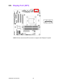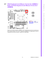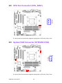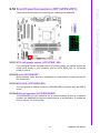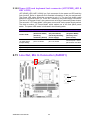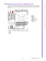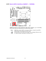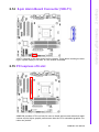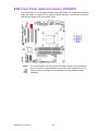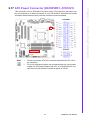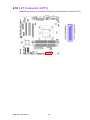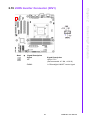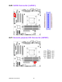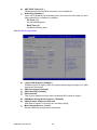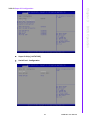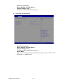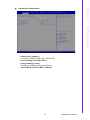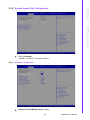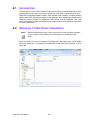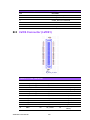
1
User Manual AIMB-584 Intel® Xeon® E3/Core™ i7/i5/i3 LGA1150 MicroATX with CRT/ DVI/eDP/LVDS/DP, 6 COM, Dual LAN, DDR3, PCIe x 16 and SATAIII Copyright The documentation and the software included with this product are copyrighted 2013 by Advantech Co., Ltd. All rights are reserved. Advantech Co., Ltd. reserves the right to make improvements in the products described in this manual at any time without notice. No part of this manual may be reproduced, copied, translated or transmitted in any form or by any means without the prior written permission of Advantech Co., Ltd. Information provided in this manual is intended to be accurate and reliable. However, Advantech Co., Ltd. assumes no responsibility for its use, nor for any infringements of the rights of third parties, which may result from its use. Acknowledgements IBM and PC are trademarks of International Business Machines Corporation. Intel® Core™ i7/i5/i3 Celeron® is trademark of Intel Corporation All other product names or trademarks are properties of their respective owners. AIMB-584 User Manual Part No. 2006058400 Edition 1 Printed in China October 2013 ii A Message to the Customer Advantech Customer Services Each and every Advantech product is built to the most exacting specifications to ensure reliable performance in the harsh and demanding conditions typical of industrial environments. Whether your new Advantech equipment is destined for the laboratory or the factory floor, you can be assured that your product will provide the reliability and ease of operation for which the name Advantech has come to be known. Your satisfaction is our primary concern. Here is a guide to Advantech’s customer services. To ensure you get the full benefit of our services, please follow the instructions below carefully. Technical Support We want you to get the maximum performance from your products. So if you run into technical difficulties, we are here to help. For the most frequently asked questions, you can easily find answers in your product documentation. These answers are normally a lot more detailed than the ones we can give over the phone. So please consult this manual first. If you still cannot find the answer, gather all the information or questions that apply to your problem, and with the product close at hand, call your dealer. Our dealers are well trained and ready to give you the support you need to get the most from your Advantech products. In fact, most problems reported are minor and are able to be easily solved over the phone. In addition, free technical support is available from Advantech engineers every business day. We are always ready to give advice on application requirements or specific information on the installation and operation of any of our products. iii AIMB-584 User Manual Declaration of Conformity FCC Class B This device complies with the requirements in part 15 of the FCC rules: Operation is subject to the following two conditions: This device may not cause harmful interference This device must accept any interference received, including interference that may cause undesired operation. This equipment has been tested and found to comply with the limits for a Class B digital device, pursuant to Part 15 of the FCC Rules. These limits are designed to provide reasonable protection against harmful interference when the equipment is operated in a commercial environment. This equipment generates, uses, and can radiate radio frequency energy and, if not installed and used in accordance with the instruction manual, may cause harmful interference to radio communications. Operation of this device in a residential area is likely to cause harmful interference in which case the user will be required to correct the interference at his/her own expense. The user is advised that any equipment changes or modifications not expressly approved by the party responsible for compliance would void the compliance to FCC regulations and therefore, the user's authority to operate the equipment. Caution! There is a danger of a new battery exploding if it is incorrectly installed. Do not attempt to recharge, force open, or heat the battery. Replace the battery only with the same or equivalent type recommended by the manufacturer. Discard used batteries according to the manufacturer's instructions. CPU Compatibility CPU Family Core Power Stepping Freq (GHz) Mfg. Tech HT L2 cache Smart cache (L3) Package Type Intel Xeon E31275 v3 QS 95W 3.5G 22nm Y NA 8MB LGA1150 PASS WG2 Intel Xeon E31225 v3 95W 3.2G 22nm - NA 8MB LGA1150 PASS WG2 Intel E3-1268L 2.3GHz 45W 2.3G 22nm Y NA 8MB LGA1150 PASS WG2/QG2 Result Supports Model Intel i7-4770S 3.1GHz QS 65W 3.1G 22nm Y NA 8 MB LGA1150 PASS QG2 Intel i7-4770TE 2.3GHz QS 45W 2.3G 22nm Y NA 8 MB LGA1150 PASS QG2 Intel i5-4570S 2.9GHz QS 65W 2.9G 22nm - NA 6MB LGA1150 PASS QG2 Intel I5-4570TE 2.7GHz 35W 2.7G 22nm Y NA 4MB LGA1150 PASS WG2/QG2 Intel i3-43300 3.5GHz 65W 3.5G 22nm Y NA 3MB LGA1150 PASS WG2/QG2 Intel I3-4330TE 2.4GHz 35W 2.4G 22nm Y NA 3MB LGA1150 PASS WG2/QG2 Intel Pentium® Processor G3420 3.2G 65W 3.2G 22nm - NA 3MB LGA1150 PASS WG2/QG2 Intel Pentium® Processor G3320TE 2.3G 35W 2.3G 22nm - NA 3MB LGA1150 PASS WG2/QG2 AIMB-584 User Manual iv Memory Compatibility Brand Size Speed Transcend 1GB DDR3 1333 Type ECC Vendor PN Memory N TS128MLK64V3U ELPIDA EDJ1108BFBG-DJPASS F DDR3 Transcend 2GB DDR3 1333 Transcend 4GB Apacer Result DDR3 N TS256MLK64V3U SEC K4B1G0846G-BCH9 PASS DDR3 1333 DDR3 N TS512MLK64V3N HYNIX H5TQ2G83CFR H9C 256x8 PASS 1GB DDR3 1333 DDR3 N 78.01GC6.AF0 H5TQ1G83DFR-H9C PASS H5TQ1G83TFR-H9C PASS Apacer 2GB DDR3 1333 DDR3 N 78.A1GDE.4200C ELPIDA J2108BCSE-DJ-F PASS Apacer 2GB DDR3 1333 DDR3 N 78.A1GDE.AF00C Hynix H5TQ2G838FR(256x8) PASS Apacer 4GB DDR3 1333 DDR3 N 78.B1GDE.AF1 HYNIX H5TQ2G83BFRH9C PASS Apacer 4GB DDR3 1333 DDR3 N 78.B1GDE.AF1 HYNIX H5TQ2G83BFR H9C PASS 256x8 Apacer 8GB DDR3 1333 DDR3 N 78.C1GEP.4210C ELPIDA J4208BASE-DJ-F 512x8 PASS Kingston 2GB DDR3 1333 DDR3 N KVR1333D3S8N9/2G ELPIDA J2108BCSE-DJF(128x8) PASS Kingston 4GB DDR3 1333 DDR3 N KVR1333D3N9/4G KINGSTON D2568JENCPGD9U(512x64 PASS ) ATP 2GB DDR3 1600 DDR3 N XQ16A8N2GS-9-AV SEC K4B2G0846D (256x8) PASS ATP 2GB DDR3 1600 DDR3 N XQ16A8N2GM-9-AV MICRON 2HM77 D9PFJ (256x8) PASS ATP 4GB DDR3 1600 DDR3 N XQ16B8N4GS-9-AV SEC K4B2G0846D (256x8) PASS ATP 8GB DDR3 1600 DDR3 N XQ16B8N8GS-9-AV SEC K4B4G0846B (512x8) PASS Apacer 8GB DDR3 1600 DDR3 N 78.C1GET.ATF0C Micron 2FD27 D9PCP (512x8) PASS DSL 2GB DDR3 1600 DDR3 N D3US56081XH12AA SEC 113 HCK0 K4B2G0846C 256x8 PASS DSL 4GB DDR3 1600 DDR3 N D3US56082XH12AA SEC 113 HCK0 K4B2G0846C 256x8 PASS Transcend 2GB DDR3 1600 DDR3 N TS256MLK64V6N MICRON IRM72 D9PFJ PASS Transcend 4GB DDR3 1600 DDR3 N TS512MLK64V6N MICRON IUM22 D9PFJ PASS Transcend 4GB DDR3 1600 DDR3 N TS512MLK64V6N MICRON 2EM77 D9PFJ 256x8 PASS Transcend 8GB DDR3 1600 DDR3 N TS1GLK64V6H micron IZD27 D9PBC 512x8 PASS Ordering Information Part Number Chipset Memory VGA DVI DP LVDS / USB eDP 3.0/2.0 SATAIII COM TPM GbE LAN AIMB-584QG200A1E Q87 Non-ECC 1 1 1 1/(1) 4/8 6 6 (1) 2 ECC/ Non1 ECC 1 1 1/(1) 4/8 6 6 (1) 2 AIMB-584WG2C226 00A1E *() means do not populated on MP version. v AIMB-584 User Manual Product Warranty (2 years) Advantech warrants to you, the original purchaser, that each of its products will be free from defects in materials and workmanship for two years from the date of purchase. This warranty does not apply to any products which have been repaired or altered by persons other than repair personnel authorized by Advantech, or which have been subject to misuse, abuse, accident or improper installation. Advantech assumes no liability under the terms of this warranty as a consequence of such events. Because of Advantech’s high quality-control standards and rigorous testing, most of our customers never need to use our repair service. If an Advantech product is defective, it will be repaired or replaced at no charge during the warranty period. For outof-warranty repairs, you will be billed according to the cost of replacement materials, service time and freight. Please consult your dealer for more details. If you think you have a defective product, follow these steps: 1. Collect all the information about the problem encountered. (For example, CPU speed, Advantech products used, other hardware and software used, etc.) Note anything abnormal and list any onscreen messages you get when the problem occurs. 2. Call your dealer and describe the problem. Please have your manual, product, and any helpful information readily available. 3. If your product is diagnosed as defective, obtain an RMA (return merchandise authorization) number from your dealer. This allows us to process your return more quickly. 4. Carefully pack the defective product, a fully-completed Repair and Replacement Order Card and a photocopy proof of purchase date (such as your sales receipt) in a shippable container. A product returned without proof of the purchase date is not eligible for warranty service. 5. Write the RMA number visibly on the outside of the package and ship it prepaid to your dealer. Initial Inspection Before you begin installing your motherboard, please make sure that the following materials have been shipped: 1 x AIMB-584 Intel LGA 1150 Xeon E3 & Core i7/i5/i3 Micro ATX Motherboard 2 x SATA HDD cable 2 x SATA Power cable 1 x I/O port bracket 1 x Startup manual 1 x Driver CD 1 x Warranty card If any of these items are missing or damaged, contact your distributor or sales representative immediately. We have carefully inspected the AIMB-584 mechanically and electrically before shipment. It should be free of marks and scratches and in perfect working order upon receipt. As you unpack the AIMB-584, check it for signs of shipping damage. (For example, damaged box, scratches, dents, etc.) If it is damaged or it fails to meet the specifications, notify our service department or your local sales representative immediately. Also notify the carrier. Retain the shipping carton and packing material for inspection by the carrier. After inspection, we will make arrangements to repair or replace the unit. AIMB-584 User Manual vi Contents Chapter 1 General Information ............................1 1.1 1.2 1.3 1.9 1.10 1.11 1.12 1.13 Introduction ............................................................................................... 2 Features .................................................................................................... 2 Specifications ............................................................................................ 2 1.3.1 System .......................................................................................... 2 1.3.2 Memory ......................................................................................... 2 1.3.3 Input/Output .................................................................................. 3 1.3.4 Graphics........................................................................................ 3 1.3.5 Ethernet LAN ................................................................................ 3 1.3.6 Industrial features ......................................................................... 3 1.3.7 Mechanical and environmental specifications............................... 3 Jumpers and Connectors .......................................................................... 4 Table 1.1: Jumpers...................................................................... 4 Table 1.2: Connectors ................................................................. 4 Board layout: Jumper and Connector Locations ....................................... 5 Figure 1.1 Jumper and Connector Location ................................ 5 Figure 1.2 I/O Connectors ........................................................... 6 AIMB-584 Board Diagram ......................................................................... 6 Figure 1.3 AIMB-584 Block Diagram ........................................... 6 Safety Precautions .................................................................................... 7 Jumper Settings ........................................................................................ 7 1.8.1 How to Set Jumpers...................................................................... 7 1.8.2 CMOS Clear (CMOS1) ................................................................. 8 Table 1.3: CMOS1....................................................................... 8 1.8.3 JLVDS1-2: LCD Power 3.3 V/ 5 V/ 12 V Selector......................... 8 Table 1.4: JLVDS1-2: LCD Power 3.3 V/5 V/ 12 V Selector ....... 8 1.8.4 JUSBPWR1-4 (USB Power Selection Connector)........................ 9 Table 1.5: JUSBPWR1-4 (USB Power Selection Connector) ..... 9 1.8.5 PSON1: ATX, AT Mode Selector .................................................. 9 Table 1.6: PSON1: ATX, AT Mode Selector................................ 9 1.8.6 JIR1+JOB1+JWD1: Watchdog Timer Output and OBS Alarm Option ........................................................................................... 9 Table 1.7: JIR1+JOB1+JWD1: Watchdog Timer Output and OBS Alarm Connector......................................................... 9 1.8.7 JME1:BIOS Update ME Mode Selector ...................................... 10 Table 1.8: BIOS update ME mode selector ............................... 10 1.8.8 JCASE1: Case Open Sensor...................................................... 10 System Memory ...................................................................................... 10 Memory Installation Procedures.............................................................. 11 Cache Memory........................................................................................ 11 Processor Installation.............................................................................. 11 PCI Bus Routing Table............................................................................ 11 2 Connecting Peripherals ....................13 2.1 2.2 Introduction ............................................................................................. 14 USB Ports (LAN1_USB01/LAN2_USB23/USB45/USB89/USB1011/ USB1213)................................................................................................ 14 Table 2.1: LAN LED Indicator.................................................... 14 USB Power Switch .................................................................................. 15 VGA/DVI-D Connector (VGA1+DVI 1) Connector................................... 16 Serial Ports (COM1~COM6) ................................................................... 17 Display Port (DP1) .................................................................................. 18 PS/2 Keyboard and Mouse Connector (KBMS1)/External PS/2 Keyboard 1.4 1.5 1.6 1.7 1.8 Chapter 2.3 2.4 2.5 2.6 2.7 vii AIMB-584 User Manual 2.11 2.12 2.13 2.14 2.15 2.16 2.17 2.18 2.19 2.20 2.21 2.22 2.23 and Mouse Connector (KBMS2) ............................................................. 19 CPU Fan Connector (CPU_FAN1) ......................................................... 20 System FAN Connector (SYSFAN1/2/3/4) ............................................. 20 Front Panel Connectors (JFP1/JFP2/JFP3) ........................................... 21 2.10.1 ATX soft power switch (JFP2/PWR_SW) ................................... 21 2.10.2 Reset (JFP2/RESET).................................................................. 21 2.10.3 HDD LED (JFP2/HDDLED) ........................................................ 21 2.10.4 External speaker (JFP2/SPEAKER) ........................................... 21 2.10.5 Power LED and keyboard lock connector (JFP1/PWR_LED & KEY LOCK)......................................................................................... 22 Table 2.2: ATX power supply LED status (No support for AT power) ............................................................................. 22 Line Out, Mic In Connector (AUDIO1) .................................................... 22 Digital Audio Connector (SPDIF_OUT1)................................................. 23 Serial ATA Interface (SATA1 ~ SATA6).................................................. 24 8-pin Alarm Board Connector (VOLT1).................................................. 25 PCI express x16 slot ............................................................................... 25 Front Panel Audio Connector (FPAUD1) ................................................ 26 ATX Power Connector (EATXPWR1, ATX12V1).................................... 27 LPT Connector (LPT1)............................................................................ 28 LVDS Inverter Connector (INV1) ............................................................ 29 LVDS Connector (LVDS1) ...................................................................... 30 General purpose I/O Connector (GPIO1) ............................................... 30 eDP Connector (eDP1) (Optional) .......................................................... 31 JTAG Connector (JTAG1)....................................................................... 31 3 BIOS Operation ................................. 33 3.1 3.2 3.4 3.5 3.6 Introduction ............................................................................................. 34 BIOS Setup ............................................................................................. 34 3.2.1 Main Menu .................................................................................. 35 3.2.2 Advanced BIOS Features ........................................................... 36 Chipset Configuration Setting ................................................................. 59 3.3.1 PCH-IO Configuration................................................................ 60 3.3.2 System Agent (SA) Configuration............................................... 65 Boot Setting ............................................................................................ 72 Security Setting....................................................................................... 73 Save & Exit Configuration ....................................................................... 74 4 Software Introduction & Service ..... 77 4.1 4.2 Introduction ............................................................................................. 78 Value-Added Software Services ............................................................. 78 4.2.1 Software API............................................................................... 78 4.2.2 Software Utility............................................................................ 80 5 Chipset Software Installation Utility 81 5.1 5.2 5.3 Before You Begin.................................................................................... 82 Introduction ............................................................................................. 82 Windows 7 Driver Setup ......................................................................... 83 6 VGA Setup ......................................... 85 6.1 6.2 Introduction ............................................................................................. 86 Windows 7 VGA Driver Installation ......................................................... 86 2.8 2.9 2.10 Chapter 3.3 Chapter Chapter Chapter AIMB-584 User Manual viii Chapter 7 LAN Configuration.............................89 7.1 7.2 7.3 7.4 Introduction ............................................................................................. 90 Features .................................................................................................. 90 Installation ............................................................................................... 90 Windows® 7 Driver Setup (Intel I217LM/ Intel I211AT) .......................... 91 Appendix A Programming the Watchdog Timer..93 A.1 Programming the Watchdog Timer ......................................................... 94 A.1.1 Watchdog Timer Overview.......................................................... 94 A.1.2 Programming the Watchdog Timer ............................................. 94 Table A.1: Watchdog Timer Registers ....................................... 96 A.1.3 Example Program ....................................................................... 97 Appendix B Pin Assignments .............................101 B.1 RS-232 Serial Port (COM2) .................................................................. 102 Table B.1: RS-232 Connector (2 x 5P Connector)................... 102 Serial Port: COM3/4/5/6 Connector (COM3456)................................... 102 Table B.2: COM3456 Connector (2 x 20 Pin Header) ............. 102 RS-232/ 422/ 485 Selection Jumpers (JSETCOM3)............................. 103 Table B.3: RS232/422/485 Selection Jumper (2 x 9 Pin Header).. 103 ................................................................................ 103 COM3_RI Selection Jumper Setting ......................... (JSETCOM3_V1)103 Table B.4: COM3_RI selection Jumper Setting ( 2 x 3 Pin Header) 104 ................................................................................ 104 LVDS Connector (LVDS1) .................................................................... 104 Table B.5: LVDS Connector..................................................... 104 Table B.11:................................................................................ 104 LVDS Panel Voltage Selection for LVDS1 Connector (JLVDS1).......... 105 Table B.6: LVDS P)anel Voltage Selection for LVDS1 Connector. 105 ................................................................................ 105 Inverter Connector for LVDS1 (INV1) ................................................... 105 Table B.7: Inverter connector for LVDS1 ( 1x 5 Pin Header)... 105 ................................................................................ 105 eDP Connector (eDP) (Optional) .......................................................... 106 Table B.8: eDP Connector (Optional) ...................................... 106 ................................................................................ 106 ATX 12 V Connector (ATX12V1) .......................................................... 106 Table B.9: ATX 4 Pin Main Power Connector (ATX12V1) ....... 106 ................................................................................ 106 ATX 24 Pin Main Power Connector (ATXPWR1).................................. 107 Table B.10: ATX 20 Pin Main Power Connector....................... 107 Serial ATA III (SATA 1 ~ 6) ................................................................... 107 Table B.11:SATA Connector..................................................... 107 CPU FAN Connector (CPUFAN1)......................................................... 108 Table B.12:CPU FAN Pin Header............................................. 108 ................................................................................ 108 SYS FAN Connector (SYSFAN1~4) ..................................................... 108 Table B.13:System Fan Connector (1 x 4 Pin Header)............. 108 ................................................................................ 108 USB 2.0 Pin Header (USB56, USB78, USB910, USB1112) ................ 108 Table B.14:Two-port USB 2.0 Header (2 x 5 Pin Header) ........ 108 USB POWER Selection for LAN1_USB12 Connector and KBMS B.2 B.3 B.4 B.5 B.6 B.7 B.8 B.9 B.10 B.11 B.12 B.13 B.14 B.15 ix AIMB-584 User Manual B.16 B.17 B.18 B.19 B.20 B.21 B.22 B.23 B.24 B.25 B.26 B.27 B.28 B.29 B.30 B.31 B.32 B.33 B.34 AIMB-584 User Manual Connector (JUSBPWR12) .................................................................... 109 Table B.15:USB Header Power Switch for LAN1_USB12 Ports .... 109 ............................................................................... 109 USB POWER Selection for LAN1_USB34 Connector (JUSBPWR34) . 109 Table B.16:USB Header Power Switch for LAN1_USB34 Ports .... 109 USB POWER Selection for USB56, USB78 Connector (JUSBPWR5678). 109 Table B.17:USB Header Power Switch for USB56, USB78 Ports .. 109 USB POWER Selection for USB910, USB1112 Connector (JUSBPWR9101112) ............................................................................ 110 Table B.18:USB Header Power Switch for USB910, USB1112 Ports ....................................................................... 110 ............................................................................... 110 Keyboard / Mouse Connector (KBMS2)................................................ 110 Table B.19:Keyboard/ Mouse Connector ( 1 x 6 Pin Header) .. 110 ............................................................................... 110 Printer Port Connector (LPT1) .............................................................. 110 Table B.20:Printer Port Connectors.......................................... 111 Digital IO Connector (GPIO1) ............................................................... 111 Table B.21:Digital IO Connector (2 x 5 Pin Header)................. 111 SMBus Connector from PCH (SMBUS1).............................................. 112 Table B.22:SMBus Connector from PCH ................................. 112 ............................................................................... 112 Audio Front Panel Connector (FPAUD1) .............................................. 112 Table B.23:Audio Front Panel Connector ................................. 112 ............................................................................... 112 SPDIF Connector (SPDIF_OUT1) ........................................................ 112 Table B.24:SPDIF Connector .................................................. 112 BIOS IC Socket (SPI1).......................................................................... 113 Table B.25:BIOS IC Socket ...................................................... 113 ............................................................................... 113 BIOS Update/Debug Connector (SPI_CN1) ......................................... 113 Table B.26:BIOS Update/Debug Connector ............................ 113 ............................................................................... 113 LAN LED (LANLED1)............................................................................ 113 Table B.27:LAN LED ............................................................... 113 Alarm Board/CMM Power Connector (VOLT1)..................................... 114 Table B.28:Alarm Board/CMM Power Connector ..................... 114 ............................................................................... 114 AT/ATX Mode Selection Connector (PSON1) ...................................... 114 Table B.29:AT/ATX Mode Selection Connector ...................... 114 ............................................................................... 114 Front Panel (PWR LED&KB LOCK#) Pin Header (JFP1) ..................... 115 Table B.30:Front Panel (PWR LED&KB LOCK#) Pin Header .. 115 ............................................................................... 115 Power Switch/ Reset/ External Speaker/ SATA HDD LED / SMBus Connector (JFP2).................................................................................. 115 Table B.31:Power Switch/ Reset/ External Speaker/ SATA HDD LED / SMBus Connector ....................................... 115 IrDA / OBS / Watch Dog Connector (JIR1+JOBS1+JWDT1) ............... 116 Table B.32:IrDA / OBS / Watch Dog Connector ....................... 116 ............................................................................... 116 RTC/CMOS Clear (JCMOS1) ............................................................... 116 Table B.33:RTC/CMOS Clear................................................... 116 ............................................................................... 116 ME Clear (JMECLR1) ........................................................................... 116 Table B.34:ME Clear ............................................................... 116 x B.35 B.36 B.37 B.38 B.39 B.40 B.41 Flash Descriptor Security Override (JMECLR1) ................................... 117 Table B.35:Flash Descriptor Security Override......................... 117 ................................................................................ 117 CASE OPEN Connector (JCASE1)....................................................... 117 Table B.36:JCASE OPEN Connector ...................................... 117 ................................................................................ 117 CASE OPEN Switch (JCASEOP_SW1)................................................ 117 Table B.37:JCASE OPEN Switch ............................................. 117 ................................................................................ 117 JTAG Connector (JTAG1)..................................................................... 118 Table B.38:JTAG CONNECTOR .............................................. 118 ................................................................................ 118 DMA Channel Assignments .................................................................. 118 Table B.39:DMA Channel Assignments.................................... 118 Interrupt Assignments ........................................................................... 118 Table B.40:Interrupt Assignments............................................. 118 1st MB Memory Map ............................................................................. 119 Table B.41:1st MB Memory Map .............................................. 119 xi AIMB-584 User Manual AIMB-584 User Manual xii Chapter 1 1 General Information 1.1 Introduction AIMB-584 is designed with the Intel Q87/C226 for industrial applications that require both performance computing and enhanced power management capabilities. The motherboard supports Intel Core i7 Xeon E3-1275v3 3.5GHz/ E3-1225v3 3.2GHz/ E3-1268L 2.3GHz/ Core i7-4770 3.1GHz/ Core i5-4570 2.9GHz/ Core i3 4330 3.5 GHz/ Pentium G3420 3.2 GHz/ Celeron G3320TE 2.3 GHz processor up to 8 MB L3 cache and DDR3 1333/1600 up to 32GB up to 16 GB. A rich I/O connectivity of 6 serial ports, 8 USB 2.0, 4 USB 3.0, dual GbE LAN, 6 SATA III ports. 1.2 Features Rich I/O connectivity: Dual GbE LAN via PCIe x1 bus, 2 x PCI 32- bit/33 MHz PCI slots, 1 x PCIe x16 slot (Gen 3), 1 x PCIe x4 slot (Gen 2), 8 USB 2.0 ports and 4 USB 3.0 ports. Standard Micro ATX form factor with industrial feature: The AIMB-584 is a full featured Micro ATX motherboard with balanced expandability and performance. Wide selection of storage devices: SATAIII HDD, customers benefit from the flexibility of using the most suitable storage device for larger capacity. Optimized integrated graphic solution: With Intel® Flexible Display Interface, it supports versatile display options and 32-bit 3D graphics engine. 1.3 Specifications 1.3.1 System CPU: Intel 4th generation Xeon E3 and Core i7/i5/i3 processor BIOS: AMI EFI 128 Mbit SPI BIOS System chipset: Intel® Q87/C226 SATA hard disk drive interface: Six on-board SATA connectors with data transmission rate up to 600 MB 1.3.2 Memory RAM: Up to 32 GB in 4 slots 240-pin DIMM sockets. Supports dual-channel DDR3 1333/1600MHz SDRAM. – AIMB-584QG2 supports non-ECC unbuffered DIMMs and do not support any memory configuration that mixes non-ECC with ECC unbuffered DIMMs. – AIMB-584WG2 supports ECC buffered DIMMs. Note! A 32-bit OS may not fully detect 4GB of RAM when 4 GB is installed. AIMB-584 User Manual 2 1.3.4 Graphics Controller: Intel® HD Graphics Display memory: 1 GB maximum shared memory with 2GB and above system memory installed DVI: Supports DVI up to resolution 1920 x 1200 @ 60Hz refresh rate VGA: Supports VGA up to resolution 2048 x 1536 @ 75Hz refresh rate LVDS: Supports LVDS up to resolution 1920 x 1200 Display Port: Support max resolution 3840 x 2160 @60Hz eDP: Support max resolution 3840 x 2160 @ 60Hz Triple Display: VGA + eDP (or LVDS)+ DP, VGA+eDP(or LVDS)+ DVI, VGA+DP+DVI Dual Display: VGA+eDP (or LVDS), VGA+DVI, eDP(or LVDS)+ DVI, VGA + DP, DP+ DVI, LVDS+DP Note! The default LVDS setting in BIOS is " disabled", customer could enable this function manually, please see detailed information in BIOS section. 1.3.5 Ethernet LAN Supports dual 10/100/1000 Mbps Ethernet port (s) via PCI Express x1 bus which provides 500 MB/s data transmission rate Controller: LAN1: Intel I217LM; LAN2:Intel I211AT 1.3.6 Industrial features Watchdog timer: Can generate a system reset. The watchdog timer is programmable, with each unit equal to one second or one minute (255 levels) 1.3.7 Mechanical and environmental specifications Operating temperature: 0 ~ 60° C (32 ~ 140° F, Depending on CPU) Storage temperature: -40 ~ 85° C (-40 ~ 185° F) Humidity: 5 ~ 95% non-condensing Power supply voltage: +3.3 V, +5 V, +12 V, -12 V, 5 Vsb 3 AIMB-584 User Manual General Information PCIe slot: 1 PCIe x16 expansion slot, 1 PCIe x4 expansion slot PCI Bus: 2 PCI slots, 32-bit/33 MHz PCI 2.2 compliant Enhanced parallel port: Configured to LPT1 or disabled. Standard DB-25 female connector cable is a optional accessory. LPT1 supports EPP/SPP/ECP. Serial port: Six serial ports, one is RS-232/422/485 with hardware auto-flow control and four are RS-232. One DB-9 connectors located in rear panel are RS-232. Keyboard and PS/2 mouse connector: Two 6-pin mini-DIN connectors are located on the mounting bracket for easy connection to PS/2 keyboard and mouse. USB port: Supports up to 8 USB 2.0 ports with transmission rates up to 480 Mbps and 4 USB 3.0 ports with transmission rates up to 5 Gbps. GPIO: AIMB-584 supports 8-bit GPIO from super I/O for general purpose control application. Chapter 1 1.3.3 Input/Output Power consumption: LAG1150 Core i7 4770S 3.1 GHz, 8MB L3 Cache, 4pcs 8GB DDR3 1600MHz memory +5 V 3.3 V 12 V 5 Vsb -12 V 2.22 A 1.13 A 5.18 A 0.49 A 0A Measure the maximum current value which system under maximum load (CPU: Top speed, RAM & Graphic: Full loading) Board size: 240 mm x 240 mm (9.6" x 9.6") Board weight: 0.365 kg 1.4 Jumpers and Connectors Connectors on the AIMB-584 motherboard link it to devices such as hard disk drives and a keyboard. In addition, the board has a number of jumpers used to configure your system for your application. The tables below list the function of each of the board jumpers and connectors. Later sections in this chapter give instructions on setting jumpers. Chapter 2 gives instructions for connecting external devices to your motherboard. Table 1.1: Jumpers Label Function JFP1 (Keyboard Lock and Power LED) Power LED Suspend: Fast flash (ATX/ AT) System Off: Slow flash (ATX) System Off: OFF (AT) System On: ON (ATX/ AT) JFP2 Power Switch/ Reset/ External Speaker/ SATA HDD LED / SMBus connector JSETCOM3 Serial port:RS232/RS422/RS485 jumper setting JCMOS1 CMOS clear (default 1-2 pin) JCASE1 case open connector JLVDS1 LVDS power jumper JIR1+JOBS1 +JWDT1 Jumper for Irda/Watchdog/OBS JME1 Jumper for flash descriptor security Override JTAG Joint Test Action Group connector 2x5 P Table 1.2: Connectors Label Function COM1 Serial Port 1 (RS-232) COM2 Serial Port COM2, pin header 2 x 5 COM3/4/5/6 Serial port: COM 3/4/5/6, box header 2x 20 p, COM3 supports RS232/422/485 DP1 Display Port Connector VGA1+DVI1 VGA Connector (Top) and DVI connector (bottom) LAN1_USB12 LAN1 & USB12 Connector LAN2_USB34 LAN2 & USB34 Connector LANLED1 Front Panel LAN Indicator connector USB5-12 USB port 5-6, 7-8, 9-10, 11-12 (internal 2 x 5 pin header on board) AIMB-584 User Manual 4 CPUFAN1 CPU FAN connector (4 pin) SYS-FAN1/2/3/4 System FAN Power Connector (4 pin) eDP1 eDP connector (2 x 10 pin header) (Optional) LVDS1 LVDS connector LPT1 Parallel port KBMS1 PS/2 keyboard and Mouse connector; Cable length: 20 meter KBMS2 On board external keyboard and Mouse connector AUDIO1 Line Out, Mic IN connector FPAUDIO1 Front Panel audio connector (FP_AU-DIO) PSON1 AT(1-2) / ATX(2-3) (Default 2-3) SPI_CN1 SPI flash programming connector GPIO1 GPIO pin header (SMD pitch=2.0 mm) SMBUS1 SMBUS expansion pin header 1 x 4 p ATX12V1 ATX 12V Auxiliary power connector EATXPWR1 ATX power connector INV1 LVDS inverter VOLT1 Voltage Display connector SPDIF1 Digital Audio connector 4 x 1 header pitch = 2.54 mm LPC1 Low pin count interface (2 x 7 pin header) 1.5 Board layout: Jumper and Connector Locations Figure 1.1 Jumper and Connector Location 5 AIMB-584 User Manual General Information Serial III ATA connector Chapter 1 SATA1-6 Figure 1.2 I/O Connectors 1.6 AIMB-584 Board Diagram Figure 1.3 AIMB-584 Block Diagram AIMB-584 User Manual 6 Warning! Always completely disconnect the power cord from chassis whenever you work with the hardware. Do not make connections while the power is on. Sensitive electronic components can be damaged by sudden power surges. Only experienced electronics personnel should open the PC chassis. Caution! The computer is provided with a battery-powered real-time clock circuit. There is a danger of explosion if battery is incorrectly replaced. Replace only with same or equivalent type recommended by the manufacturer. Discard used batteries according to manufacturer's instructions. Caution! There is a danger of a new battery exploding if it is incorrectly installed. Do not attempt to recharge, force open, or heat the battery. Replace the battery only with the same or equivalent type recommended by the manufacturer. Discard used batteries according to the manufacturer’s instructions. 1.8 Jumper Settings This section provides instructions on how to configure your motherboard by setting the jumpers. It also includes the motherboards's default settings and your options for each jumper. 1.8.1 How to Set Jumpers You can configure your motherboard to match the needs of your application by setting the jumpers. A jumper is a metal bridge that closes an electrical circuit. It consists of two metal pins and a small metal clip (often protected by a plastic cover) that slides over the pins to connect them. To “close” (or turn ON) a jumper, you connect the pins with the clip. To “open” (or turn OFF) a jumper, you remove the clip. Sometimes a jumper consists of a set of three pins, labeled 1, 2, and 3. In this case you connect either pins 1 and 2, or 2 and 3. A pair of needle-nose pliers may be useful when setting jumpers. 7 AIMB-584 User Manual General Information Caution! Always ground yourself to remove any static charge before touching the motherboard. Modern electronic devices are very sensitive to electrostatic discharges. As a safety precaution, use a grounding wrist strap at all times. Place all electronic components on a static-dissipative surface or in a static-shielded bag when they are not in the chassis. Chapter 1 1.7 Safety Precautions 1.8.2 CMOS Clear (CMOS1) The AIMB-584 motherboard contains a jumper that can erase CMOS data and reset the system BIOS information. Normally this jumper should be set with pins 1-2 closed. If you want to reset the CMOS data, set CMOS1 to 2-3 closed for just a few seconds, and then move the jumper back to 1-2 closed. This procedure will reset the CMOS to its default setting. Table 1.3: CMOS1 Function Jumper Setting *Keep CMOS data 1-2 closed Clear CMOS data 2-3 closed * Default 1.8.3 JLVDS1-2: LCD Power 3.3 V/ 5 V/ 12 V Selector Table 1.4: JLVDS1-2: LCD Power 3.3 V/5 V/ 12 V Selector Closed Pins Result JLVDS2, 1-2 Jumper for +3.3 V JLVDS2, 2-3 Jumper for +V5 JLVDS1, 2 JLVDS2, 2 Jumper for +12 V *Default AIMB-584 User Manual 8 Table 1.5: JUSBPWR1-4 (USB Power Selection Connector) Pin Pin Name 1 +V5_DUAL 2 +V5_USB 3 +V5 General Information 1 Default: 2-3 Pin (+5 V) 1.8.5 PSON1: ATX, AT Mode Selector Table 1.6: PSON1: ATX, AT Mode Selector Closed Pins Result 1-2 AT Mode 2-3* ATX Mode *Default 1 1 ATX Mode 2-3 closed AT Mode 1-2 closed 1.8.6 JIR1+JOB1+JWD1: Watchdog Timer Output and OBS Alarm Option Table 1.7: JIR1+JOB1+JWD1: Watchdog Timer Output and OBS Alarm Connector Pin Pin Name 1 +V5 2 NC 3 NC 4 Watch dog reset# output 5 IRRX 6 System reset input# 7 GND 8 SIO Warning Beep output 9 IRTX 10 SP1 Buzzer Beep input Note: Watch dog time-out reset# (4-6 short) / SIO Warning Beep enable (8-10 short). 9 Chapter 1 1.8.4 JUSBPWR1-4 (USB Power Selection Connector) AIMB-584 User Manual 1.8.7 JME1:BIOS Update ME Mode Selector JME1 is the jumper for users to select BIOS update freely without lock protection when using ADVSPI or with lock protection. Table 1.8: BIOS update ME mode selector Function Jumper BIOS Setting protect Master ME JME1 Region Update ME function PWR Setting Access tool version after working Control update status 1.*Production mode (1-2) pin None closed FF Link/ ADVSPI updated remote control Lock Link/ no Read:0B ADVSPI remote updated Write:0A control 2. 3. Manufacture (2-3) pin None mode closed FF OEM request ADVSPI updated None default AC on/ stdby AC on/ stdby None None * refers to default. 1. 2. 3. * In default production mode, there's no lock protection for BIOS. The Master Region Access Control setting is FF, users can update the complete BIOS with the ADVSPI tool. The function is same as Manufacture mode. BIOS ME (Management Engine) function keeps link/remote control. The jumper can be set under AC off PWR status, it can not be set under standby PWR status. In production mode with lock protection for BIOS, the Master Region Access Control setting is Read:0B, Write:0A. Users can not update BIOS ME firmware freely. BIOS ME (Management Engine) function keeps link/remote control. This setting is only for OEM project requests. The jumper can be set under AC off PWR status, it can not set under standby PWR status. In manufacture mode, BIOS has no lock protection function. The Master Region Access Control setting is FF, users can update complete BIOS with ADVSPI tool. However, the BIOS ME function does not keep the link/remote control after the BIOS been updated. 1.8.8 JCASE1: Case Open Sensor The AIMB-584 motherboard contains a jumper that provides a chassis open sensor. The buzzer on the motherboard beeps when the case is opened. 1.9 System Memory AIMB-584 has four 240-pin memory sockets for 1333/1600 MHz memory modules with maximum capacity of 32 GB (Maximum 8 GB for each DIMM). AIMB-584QG2 supports only non-ECC DDR3 memory modules and do not support registered DIMMs (RDIMMs) Note! Because AIMB-584 supports Intel Active Management Technology 8.0 (iAMT 8.0) which utilizes some memory space of channel 0, it's suggested that the user should not leave channel 0 DIMM slots (DIMMA1 and DIMMA2) empty, or it may cause some system abnormality. AIMB-584 User Manual 10 To install DIMMs, first make sure the two handles of the DIMM socket are in the “open” position, i.e., the handles lean outward. Slowly slide the DIMM module along the plastic guides on both ends of the socket. Then firmly but gently (avoid pushing down too hard) press the DIMM module well down into the socket, until you hear a click when the two handles have automatically locked the memory module into the correct position of the DIMM socket. To remove the memory module, just push both handles outward, and the memory module will be ejected by the mechanism. The AIMB-584 supports a CPU with one of the following built-in full speed L3 caches: 8MB for Intel Xeon E3 1275v3 8MB for Intel Xeon E3 1225v3 8MB for Intel Xeon E3 1268L 8MB for Intel Core i7 4770S 8MB for Intel Core i7 4770TE 6MB for Intel Core i5 4570S 4MB for Intel Core i5 4570TE 3MB for Intel Core i3 4330 3MB for Intel Core i3 4330TE 3MB for Intel Pentium G3420 3MB for Intel Celeron G3320TE The built-in second-level cache in the processor yields much higher performance than conventional external cache memories. 1.12 Processor Installation The AIMB-584 is designed for LGA1150, Intel Xeon and Intel Core i7/Core i5/Core i3/ Pentium processor. 1.13 PCI Bus Routing Table PCI1 PCI2 AD16 AD17 A A B B B C C C D D D A AD PCI slot INT 11 AIMB-584 User Manual General Information 1.11 Cache Memory Chapter 1 1.10 Memory Installation Procedures AIMB-584 User Manual 12 Chapter 2 Connecting Peripherals 2 2.1 Introduction You can access most of the connectors from the top of the board as it is being installed in the chassis. If you have a number of cards installed or have a packed chassis, you may need to partially remove the card to make all the connections. 2.2 USB Ports (LAN1_USB01/LAN2_USB23/USB45/ USB89/USB1011/USB1213) The AIMB-584 provides up to 12 USB ports. The USB interface complies with USB Specification Rev 2.0 supporting transmission rates up to 480 Mbps and Rev 3.0 supporting transmission rate up to 5 Gbps and is fuse protected. The USB interface can be disabled in the system BIOS setup. The AIMB-584 is equipped with two high-performance 1000 Mbps Ethernet LAN adapters, both of which are supported by all major network operating systems. The RJ-45 jacks on the rear panel provides convenient LAN connection. LAN1_USB12 LAN2_USB34 Table 2.1: LAN LED Indicator LAN Mode LAN1 indicator LAN2 indicator AIMB-584 User Manual LAN Indicator LED1 (Right) off for mal-link; Link (On) / Active (Flash) LED2 (Left) 100 Mbps (On) / 10 Mbps (Off) LED2 (Left) 1000 Mbps (On) LED1 (Right) off for mal-link; Link (On) / Active (Flash) LED2 (Left) 100 Mbps (On) / 10 Mbps (Off) LED2 (Left) 1000 Mbps (On) 14 AIMB-584 allows users to set USB power between +5 VSB and +5 V. When the jumper is set as +5 V (default 2-3 pin), the board doesn't support wake from S3 via keyboard or mouse. If you need to set it to +5 Vsb, you need to modify the jumper (12 pin) and modify the customized BIOS at the same time. Chapter 2 2.3 USB Power Switch Connecting Peripherals Note! When USB power is switched to +5V, it can't be connected with power KVM. 15 AIMB-584 User Manual 2.4 VGA/DVI-D Connector (VGA1+DVI 1) Connector 5 10 15 1 6 11 AIMB-584 includes VGA and DVI interfaces that can drive conventional VGA and DVI displays. VGA is a standard 15-pin D-SUB connector commonly used for VGA. Pin assignments for VGA and DVI connectors are detailed in Appendix B. AIMB-584 User Manual 16 Chapter 2 2.5 Serial Ports (COM1~COM6) COM1 Connecting Peripherals AIMB-584 supports six serial ports. COM1, COM2, COM4-6 supports RS-232. COM3 supports RS-232/422/485 (with 5V/12V power). JSETCOM3 is used to select the RS232/422/485 mode for COM3. These ports can connect to serial devices, such as a mouse or a printer, or to a communications network. The IRQ and address ranges for both ports are fixed. However, if you want to disable the port or change these parameters later, you can do this in the system BIOS setup. Different devices implement the RS-232 standards in different ways. If you have problems with a serial device, be sure to check the pin assignments for the connector. 17 AIMB-584 User Manual 2.6 Display Port (DP1) AIMB-584 has one external DP connector to supports the Display Port panel. AIMB-584 User Manual 18 Chapter 2 2.7 PS/2 Keyboard and Mouse Connector (KBMS1)/ External PS/2 Keyboard and Mouse Connector (KBMS2) Connecting Peripherals Two 6-pin mini-DIN connectors (KBMS1) on the motherboard provide connection to a PS/2 keyboard and a PS/2 mouse, respectively. KBMS2 is for supporting the 2nd PS/ 2 keyboard and PS/2 mouse by a cable P/N 1700018699. 19 AIMB-584 User Manual 2.8 CPU Fan Connector (CPU_FAN1) If a fan is used, this connector supports cooling fans of 500 mA (6 W) or less. 2.9 System FAN Connector (SYSFAN1/2/3/4) If a fan is used, this connector supports cooling fans of 500 mA (6 W) or less. AIMB-584 User Manual 20 There are several headers for monitoring and controlling the AIMB-584. Connecting Peripherals 2.10.1 ATX soft power switch (JFP2/PWR_SW) If your computer case is equipped with an ATX power supply, you should connect the power on/off button on your computer case to (JFP2/ PWR_SW), for convenient power on and off. 2.10.2 Reset (JFP2/RESET) Many computer cases offer the convenience of a reset button. Connect the wire for the reset button. 2.10.3 HDD LED (JFP2/HDDLED) You can connect an LED to connector (JFP2/HDDLED) to indicate when the HDD is active. 2.10.4 External speaker (JFP2/SPEAKER) JFP2/SPEAKER is a 4-pin connector for an external speaker. If there is no external speaker, the AIMB-584 provides an onboard buzzer as an alternative. To enable the buzzer, set pins 7 & 10 as closed. 21 Chapter 2 2.10 Front Panel Connectors (JFP1/JFP2/JFP3) AIMB-584 User Manual 2.10.5 Power LED and keyboard lock connector (JFP1/PWR_LED & KEY LOCK) (JFP1/PWR_LED & KEY LOCK) is a 5-pin connector for the power on LED and Key Lock function. Refer to Appendix B for detailed information on the pin assignments. The Power LED cable should be connected to pin 1-3. The key lock button cable should be connected to pin 4-5. There are 3 modes for the power supply connection. The first is “ATX power mode”; the system turns on/off by a momentary power button. The second is “AT Power Mode”; the system turns on/off via the power supply switch. The third is another “AT Power Mode” which makes use of the front panel power switch. The power LED status is indicated in the following table: Table 2.2: ATX power supply LED status (No support for AT power) Power mode LED (ATX Power Mode) (On/off by momentary button) LED (AT power Mode) (On/off by switching power supply) LED (AT power Mode) (On/off by front panel switch) PSON1 (on back plane) jumper setting pins 2-3 closed pins 1-2 closed Connect pins 1 & 2 to panel switch via cable System On On On On System Suspend Fast flashes Fast flashes Fast flashes System Off Slow flashes Off Off 2.11 Line Out, Mic In Connector (AUDIO1) Line Out Mic In AIMB-584 User Manual 22 This connector is for the S/PDIF audio module to allow digital output sound. Connect one end of the S/PDIF audio cable to this connector and the other end to the S/PDIF module. Chapter 2 2.12 Digital Audio Connector (SPDIF_OUT1) Connecting Peripherals Note! The S/PDIF module is purchased separately. 23 AIMB-584 User Manual 2.13 Serial ATA Interface (SATA1 ~ SATA6) AIMB-584 features a high performance Serial ATA III interface (up to 600 MB/s) which eases hard drive cabling with thin, space-saving cables. Note! AIMB-584 on board SATA only supports Fedora 14 and 15 and SATA mode in BIOS should be set as AHCI mode. If SATA mode is set as IDE mode, when user is installing Fedora 14 and 15, ODD has been connected on SATA port 3~6. AIMB-584 User Manual 24 2.15 PCI express x16 slot AIMB-584 provides a PCIe x16 slot for users to install add-on cards when their applications require higher graphic performance than the CPU embedded graphics controller can provide. 25 AIMB-584 User Manual Connecting Peripherals VOLT1 connects to the alarm board on the chassis. These alarm boards give warnings if a power supply or fan fails, or if the chassis overheats. Chapter 2 2.14 8-pin Alarm Board Connector (VOLT1) 2.16 Front Panel Audio Connector (FPAUD1) This connector is for a chassis-mounted front panel audio I/O module that supports either HD Audio or legacy AC’97 (optional) audio standard. Connect this connector with the front panel audio I/O module cable. Note! For motherboards with the optional HD Audio feature, we recommend that you connect a high-definition front panel audio module to this connector to take advantage of the motherboard’s high definition audio capability. AIMB-584 User Manual 26 This connector is for an ATX Micro-Fit power supply. The plugs from the power supply are designed to fit these connectors in only one direction. Determine the proper orientation and push down firmly until the connectors mate completely. EATXPWR1 Note! 1. 2. Please connect the ATX12V1 connector with the PSU ATX 12V 4pin connector. For a fully configured system, we recommend that you use a power supply unit (PSU) that complies with ATX 12 V Specification 2.0 (or later version) and provides a minimum power of 180 W. 27 AIMB-584 User Manual Connecting Peripherals ATX12V1 Chapter 2 2.17 ATX Power Connector (EATXPWR1, ATX12V1) 2.18 LPT Connector (LPT1) AIMB-584 has one 2x 13 pin header on board for print port device connection (LPT1). AIMB-584 User Manual 28 Signal Description Signal VR Signal Description Vadj=0.75 V (Recommended: 4.7 KΩ, >1/16 W) LCD backlight ON/OFF control signal ENBKL 29 AIMB-584 User Manual Connecting Peripherals Note! Chapter 2 2.19 LVDS Inverter Connector (INV1) 2.20 LVDS Connector (LVDS1) 2.21 General purpose I/O Connector (GPIO1) AIMB-584 User Manual 30 Chapter 2 2.22 eDP Connector (eDP1) (Optional) Connecting Peripherals 2.23 JTAG Connector (JTAG1) 31 AIMB-584 User Manual AIMB-584 User Manual 32 Chapter 3 BIOS Operation 3 3.1 Introduction AMI BIOS has been integrated into many motherboards, and has been very popular for over a decade. With the AMI BIOS Setup program, you can modify BIOS settings to control the special features of your computer. The Setup program uses a number of menus for making changes. This chapter describes the basic navigation of the AIMB-584 setup screens. 3.2 BIOS Setup The AIMB-584 Series system has AMI BIOS built in, with a SETUP utility that allows users to configure required settings or to activate certain system features. The SETUP saves the configuration in the FLASH of the motherboard. When the power is turned off, the battery on the board supplies the necessary power to preserve the FLASH. When the power is turned on, press the <Del> or <Esc> button during the BIOS POST (Power-On Self Test) to access the CMOS SETUP screen. Control Keys < ← >< → > Select Screen < ↑ >< ↓ > Select Item <Enter> Select <+/-> Change Opt <F1> General help <F2> Previous Values <F3> Optimized Defaults <F4> Save & Exit <Esc> Exit AIMB-584 User Manual 34 Press <Del> or <Esc> to enter AMI BIOS CMOS Setup Utility, the Main Menu will appear on the screen. Use arrow keys to select among the items and press <Enter> to accept or enter the sub-menu. Chapter 3 3.2.1 Main Menu BIOS Operation The Main BIOS setup screen has two main frames. The left frame displays all the options that can be configured. Grayed-out options cannot be configured; options in blue can. The right frame displays the key legend. Above the key legend is an area reserved for a text message. When an option is selected in the left frame, it is highlighted in white. Often a text message will accompany it. System time / System date Use this option to change the system time and date. Highlight System Time or System Date using the <Arrow> keys. Enter new values through the keyboard. Press the <Tab> key or the <Arrow> keys to move between fields. The date must be entered in MM/DD/YY format. The time must be entered in HH:MM:SS format. 35 AIMB-584 User Manual 3.2.2 Advanced BIOS Features Select the Advanced tab from the AIMB-584 setup screen to enter the Advanced BIOS Setup screen. You can select any of the items in the left frame of the screen, such as CPU Configuration, to go to the sub menu for that item. You can display an Advanced BIOS Setup option by highlighting it using the <Arrow> keys. All Advanced BIOS Setup options are described in this section. The Advanced BIOS Setup screen is shown below. The sub menus are described on the following pages. AIMB-584 User Manual 36 Chapter 3 3.2.2.1 PCI Subsystem Settings BIOS Operation PCI Latency Time: [32 PCI Bus Clocks] The value to be programmed in PCI Latency Timer Register. VGA Palette Snoop [Disable] Enables or Disables VGA Palette Registers Snooping. PERR# Generation [ Disable] Enables or Disables PCI Device to Generate PERR#. SERR# Generation [ Disable] Enables or Disables PCI Device to Generate SERR#. 37 AIMB-584 User Manual PCI Express Settings – Relaxed Ordering [Disable] Enables or Disables PCI Express Device Relaxed Ordering. – Extended Tag [ Disabled ] Enable allows Device to use 8-bit Tag field as a requester. – No Snoop [ Enabled ] Enables or Disables PCI Express Device No Snoop option. – Maximum Payload [ Auto ] Set Maximum Payload of PCI Express Device or allow System BIOS to select the value, and the default is "Auto". – Maximum Read Request [ Auto ] Set Maximum Read Request Size of PCI Express Device or allow System BIOS to select the value. – ASPM Support [ Disabled ] Set the ASPM Level: Force L0s - Force all links to L0s State. AUTO - BIOS auto configure DISABLE - Disables ASPM – Extended Synch [ Disabled ] Enable allows generation of Extended Synchronization patterns. – Link Training Retry Defines number of Retry Attempts software will take to retrain the link if previous training attempt was unsuccessful. – Link Training Timeout (uS) Defines number of Microseconds software will wait before polling 'Link Training' bit in Link Status register. Value range from 10 to 10000 uS. – Unpopulated Links [ Keep Link On ] In order to save power, software will disable unpopulated PCI Express links, if this option set to 'Disable Link'. AIMB-584 User Manual 38 Warning! Enabling this may cause issues with other hardware after S3 resume. BIOS Operation 3.2.2.2 ACPI Settings Chapter 3 – Restore PCIE Registers [Disabled ] On non-PCI Express aware OS's (Pre Windows Vista) some devices may not be correctly re-initialized after S3. Enabling this restore PCI Express device configurations on S3 resume. Enable ACPI Auto Configuration [ Disabled] Enable or disable BIOS ACPI auto configuration. Enable Hibernation [ Enabled ] Enables or Disables System ability to Hibernate (OS/S4 Sleep State). This option may be not effective with some OS. ACPI Sleep State [ Auto ] Select ACPI sleep state the system will enter when the SUSPEND button is pressed. Lock Legacy Resources [ Disabled ] Enables or Disables Lock of Legacy Resources. S3 Video Repost [ Disabled ] Enable or Disable S3 Video Repost. 39 AIMB-584 User Manual 3.2.2.3 Trusted Computing To enable/disable TPM (TPM 1.1/1.2) set up in BIOS. TPM (Trusted Platform Module) is a secure key generator and key cache management component, enables protected storage of encryption keys and authentication credentials for enhanced security capabilities. Security Device Support [ Disable ] Note! TCG EFI Protocol and INT1A interface won't be available. AIMB-584 User Manual 40 Chapter 3 3.2.2.4 S5RTC Wake Settings The item allow you enable or disable system wake up on alarm event. BIOS Operation Wake system with Fixed Time [ Disabled ] Note! When enabled, system will wake up on the specified time. 41 AIMB-584 User Manual 3.2.2.5 CPU Configuration CPU Configuration The item shows you CPU specification and feature, the content could be different by the different CPU. AIMB-584 User Manual 42 Chapter 3 3.2.2.6 SATA Configuration BIOS Operation SATA Controllers [ Enabled ] Enable or disable SATA Function. SATA Mode [ IDE ] This can be configured as IDE, AHCI or RAID mode. 43 AIMB-584 User Manual 3.2.2.7 Intel Rapid Start Technology Intel Rapid Start Technology [ Disabled ] AIMB-584 User Manual 44 Chapter 3 3.2.2.8 PCH FM Configuration BIOS Operation MEDS BIOS Status Code [ Disable ] Firmware update Configuration – ME FW Image Re-Flash [ Disabled ] 45 AIMB-584 User Manual 3.2.2.9 Intel® Anti-Theft Technology Configuration Intel( R ) Anti-Theft Technology Configuration [ Enabled ] Enter Intel ( R ) AT Suspend Mode [ Disabled ] AIMB-584 User Manual 46 Chapter 3 3.2.2.10 AMT Configuration BIOS Operation Intel AMT [ Enabled ] This item allows users to enable or disable Intel AMT BIOS extension. BIOS Hotkey Pressed [ Disabled ] Enable/Disable BIOS hotkey press. MEBx Select Screen [ Disabled ] Enable/Disable MEBx selection screen. Hide Un-Configure ME Confirmation [ Disabled ] Hide Un-Configure ME without password Confirmation Prompt. MEBx Debug Message Output [ Disabled ] Enable MEBx debug message output. Un-Configure ME [ Disabled ] Sets this item to [Disabled] to unconfigure AMT/ME without using a password or set it as [Enabled] to use a password. Amt Wait timer [0] Set timer to wait before sending ASF_GET_BOOT_OPTIONS. Disable ME [ Disabled ] Set ME to Soft Temporary Disabled. ASF [ Enabled ] Enable/Disable Alert Specification Format. Active Remote Assistance Process [ Disabled ] Trigger CIRA boot. USB Configure [ Enable ] Enable/Disable USB Configure function. PET Progress [ Enable ] User can Enable/Disable PET Events progress to receive PET events or not. 47 AIMB-584 User Manual AMT CIRA Timeout [ 0 ] OEM defined timeout for MPS connection to be established. Watchdog [ Disabled ] When set to [Enabled], the Watchdog timer will monitor the time taken for each task performed by a software or hardware. – OS Timer [ 0 ] Set OS watchdog timer. – BIOS Timer [ 0] Set BIOS watchdog timer. 3.2.2.11 USB Configuration Legacy USB Support [ Enabled ] Enables support for legacy USB. Auto option disables legacy support if no USB devices are connected. USB 3.0 Support [ Enabled ] XHCI Hand-off [ Enabled ] EHCI Hand-off This is just a workaround item under OS without EHCI hand-off support. USB Mass Storage Driver Support [ Enabled ] USB hardware delays and time-outs USB Device transfer & reset time-out and delay setting. Mass Storage Devices [ Auto ] Shows USB mass storage device information. AIMB-584 User Manual 48 Chapter 3 3.2.2.12 Super IO Configuration BIOS Operation Super IO Chip [ NCT6776D ] Serial Port 1 Configuration 49 AIMB-584 User Manual – Serial Port [ Enabled ] – Device Settings: IO=3F8h; IRQ =4 – Change Settings [ Auto ] To select an optimal setting for serial port 1. Serial Port 2 Configuration – Serial Port [ Enabled ] – Device Settings: IO=378h; IRQ =3 – Change Setting [ Auto ] To select an optimal setting for serial port 2. – Device Mode Serial port 2 could be selected as “Standard serial port mode”, “IrDA 1.0 (HP SIR) mode”, or “ASKIR mode”. AIMB-584 User Manual 50 Parallel Port Configuration Chapter 3 BIOS Operation – Parallel Port [ Enabled ] To enable or disable Parallel Port. (LPT/LPTE) – Device Settings: IO=278h; IRQ =7 – Change Settings [ Auto ] To select an optimal setting for parallel port. – Device Mode [ ECP and EPP 1.9 Mode ] 51 AIMB-584 User Manual Digital I/O Configuration – Digital I/O Pin 1 - 8 [ Input ] 3.2.2.13 H/W Monitor Smart Fan Mode Configuration AIMB-584 User Manual 52 CPU FAN Mode [ SMART FAN IV Mode ] The item shows you CPU temperature and fan speed (PWM) information. SYSFAN Mode [ SMART FAN IV Mode ] The item shows you system temperature and fan speed (PWM) information. PC Health Status Chapter 3 BIOS Operation – CPU Warning Temperature [ Disabled ] Use this to set the CPU warning temperature threshold. When the system reaches the warning temperature, the speaker will beep. – ACPI Shutdown Temperature [ Disabled ] Use this to set the ACPI shutdown temperature threshold. When the system reaches the shutdown temperature, it will be automatically shut down by ACPI OS to protect the system from overheating damage. 53 AIMB-584 User Manual 3.2.2.14 Second Super IO Configuration AIMB-584 supports 2nd super IO for COM 3-6, so this page of the BIOS menu is to set respective serial port configuration. Serial Port 3 Configuration – Serial Port [ Enabled ] To “enable or disable” Serial Port 3. – Device Settings: IO=C80h; IRQ =10 – Change Settings [ Auto ] To select an optimal setting for serial port 3. – Auto flow control [ Disabled ] When the COM is to set as RS-485, it supports auto flow control function. AIMB-584 User Manual 54 Serial Port 4 Configuration Chapter 3 BIOS Operation – Serial Port [Enabled] To "enable or disable" serial port 4. – Device Settings: IO=C88h; IRQ =10 – Change Settings [ Auto ] To select an optimal setting for serial port 4. 55 AIMB-584 User Manual Serial Port 5 Configuration – Serial Port [Enabled] To “enable or disable” serial port 5. – Device Settings: IO=C90h; IRQ =10 – Change Settings [ Auto ] To select an optimal setting for serial port 5. AIMB-584 User Manual 56 Serial Port 6 Configuration Chapter 3 BIOS Operation – Serial Port [ Enabled ] To “enable or disable” serial port 6. – Device Settings: IO=C98h; IRQ =10 – Change Setting [ Auto ] To select an optimal setting for serial port 6. 57 AIMB-584 User Manual 3.2.2.15 Serial Port Console Redirection Console Redirection [ Enabled ] Enable or disable the console redirection feature AIMB-584 User Manual 58 Select the chipset tab from the BIOS setup screen to enter the Chipset Setup screen. Users can select any item in the left frame of the screen, such as PCI express Configuration, to go to the sub menu for that item. Users can display a Chipset Setup option by highlighting it using the <Arrow> keys. All Chipset Setup options are described in this section. The Chipset Setup screens are shown below. The sub menus are described on the following pages. Chapter 3 3.3 Chipset Configuration Setting BIOS Operation 59 AIMB-584 User Manual 3.3.1 PCH-IO Configuration PCI Express Configuration Details of PCI Express items. (See 3.3.1.1) USB Configuration Details of USB items. (See 3.3.1.2) PCH Azalia Configuration Details of PCH azalia items. (See 3.3.1.3) LAN 1controller [ Enabled ] Enable or disable the LAN 1 controller. – LAN 1 PXE OpROM [ Disabled ] Enable or disable the LAN 1 option-ROM. – Wake on LAN [ Disabled ] Enable or disable integrated LAN to wake the system. (The Wake On LAN cannot be disabled if ME is on at Sx state) LAN 2 controller [ Enabled ] Enable or disable the LAN 2 controller. – LAN 2 PXE OpROM [ Disabled ] Enable or disable the LAN 2 option-ROM. PCIE Wake [ Disabled ] Enable or disable PCIE to wake the system from S5. DeepSx Power Policies Enable or Disable Deep Sleep mode. Restore AC Power Loss [ Power Off ] This item allows users to select off, on and last state. AIMB-584 User Manual 60 Chapter 3 3.3.1.1 PCI Express Configuration BIOS Operation PCI Express Clock Gating [ Enabled ] Enable or Disable PCI Express clock gating for each port. DMI Link ASPM Control [ Enabled ] The control of Active State Power Management on both NB side and SB side of the DMI Link. DMI Link Extended Synch Control [ Disabled ] The control of Extended Synch on SB side of the DMI Link. PCIe-USB Glitch W/A [ Disabled ] PCIe-USB Glitch W/A for bad USB device(s) connected behind PCIE/PEG Port. PCIE Root Port Function Swapping [ Disabled ] Enable or disable PCI Express PCI Express Root Port Function Swapping. Subtractive Decode [ Disabled ] Enable or disable PCI Express Subtractive Decode. 61 AIMB-584 User Manual PCI Express Root Port 1 – PCI Express Root Port 1 [ Enabled ] Control the PCI Express Root Port. – ASPM Support [ Auto ] Set the ASPM Level: Force L0s - Force all links to L0s State : AUTO - BIOS auto configure : DISABLE - Disables ASPM – L1 Substates PCI Express L1 Substates settings. URR [ Disabled ]: Enable or disable PCI Express Unsupported Request Reporting. FER [ Disabled ]: Enable or disable PCI Express Device Fatal Error Reporting. NFER [ Disabled ]: Enable or disable PCI Express Device Non-Fatal Error Reporting. CER [ Disabled ]: Enable or disable PCI Express Device Correctable Error Reporting. CTO [ Disabled ]: Enable or disable PCI Express Completion Timer TO. SEFE [ Disabled ]: Enable or disable Root PCI Express System Error on Fatal Error. SENFE [ Disabled ]: Enable or disable Root PCI Express System Error on Non-Fatal Error. SECE [ Disabled ]: Enable or disable Root PCI Express System Error on Correctable Error. PME SCI [ Disabled ]: Enable or disable PCI Express PME SCI. Hot Plug [ Disabled ]: Enable or disable PCI Express Hot Plug. – PCIe Speed [ Auto ] Select PCI Express port speed. AIMB-584 User Manual 62 USB Preconditon [ Disabled ] To enable or disable precondition work on USB host controller for faster enumeration. XHCI Mode [ Auto ] Mode of operation of XHCI controller. BTCG [ Enabled ] Enable/Disable trunk clock gating. 63 AIMB-584 User Manual BIOS Operation 3.3.1.2 USB Configuration Chapter 3 – Detect Non-Compliance Device [ Disabled ] Detect Non-Compliance PCI Express Device. If enable, it will take more time at POST time. – Extra Bus Reserved Extra Bus Reserved (0-7) for bridges behind this Root Bridge. – Reserved Memory => Reserved Memory Range for this Root Bridge. – Prefetchable Memory => Prefetchable Memory Range for this Root Bridge. – Reserved I/O => Reserved I/O (4K/8K/12K/16K/.../48K) Range for this Root Bridge. 3.3.1.3 PCH Azalia Configuration Azalia [ Auto] This item set for control Detection of the Azalia device. [Disabled] = Azalia will be unconditionally disabled. [Enabled] = Azalia will be unconditionally enabled [Auto] = Azalia will be enabled if present, disabled otherwise. AIMB-584 User Manual 64 Chapter 3 3.3.2 System Agent (SA) Configuration BIOS Operation VT-d [ Enabled ] Disable or enable VT-d function on MCH. 3.3.2.1 Graphics Configuration Graphics Turbo IMON Current [ 14-31 ] 65 AIMB-584 User Manual Primary Display [ Auto ] Select which of IGFX/PEG/PCI Graphics device should be Primary Display Internal Graphics [ Auto ] Keep IGD enabled based on the setup options. Aperture Size [ 256MB ] DVMT Pre-Allocated [ 32M ] Select DVMT 5.0 Pre-Allocated (Fixed) Graphics Memory size used by the Internal Graphics Device. DVMT Total Gfx Mem [ 256M ] Select DVMT5.0 Total Graphic Memory size used by the Internal Graphics Device. Gfx Low Power Mode [ Enabled ] Note! This option is applicable for SFF only. LCD control Primary IGFX Boot Display [ VBIOS Default ] Select the video device which will be activated during POST. Secondary boot display selection will appear based on customer's selection. Note! When BIOS set as " Auto", only CRT is supported as the single display under DOS. AIMB-584 User Manual 66 The triple display can only working PASS under Windows 7 and 8, the 2nd and 3rd display can not work under DOS. Here is 2-3 displays combination table and all of these combinations are verified and tested properly already. Display Combination List BIOS DOS WES 7 CRT PASS PASS PASS DVI PASS PASS PASS DP PASS PASS PASS EDP PASS PASS PASS LVDS PASS PASS PASS CRT+DVI NA NA PASS CRT+LVDS NA NA PASS CRT+DP NA NA PASS CRT+EDP NA NA PASS DVI+LVDS NA NA PASS DVI+DP NA NA PASS DVI+EDP NA NA PASS LVDS+DP NA NA PASS LVDS+EDP NA NA PASS DP+LVDS+DVI NA NA PASS CRT+LVDS+DVI NA NA PASS CRT+DP+LVDS NA NA PASS DP+EDP+DVI NA NA PASS CRT+EDP+DVI NA NA PASS CRT+DP+EDP NA NA PASS CRT+DP+DVI NA NA PASS Chapter 3 Note! Single Display Triple Display LVDS Panel Type [ Disabled ] Note! When you enable LVDS type, customers can choose different resolution settings from the table. Default resolution setting is "800 x 600 18-bit". 67 AIMB-584 User Manual BIOS Operation Dual Display Backlight Signal Control [ PWM ] Switch Backlight Signal Control for PWM or LINEAR. LVDS/eDP Select [ LVDS ] Select the Active LFP Configuration. Note! LVDS and eDP co-layout designed on AIMB-584, and the default setting in BIOS and HW both are LVDS. If customer would like to active eDP function, then both of HW and BIOS need to be modified. AIMB-584 User Manual 68 Chapter 3 3.3.2.2 DMI Configuration BIOS Operation DMI Vc1 Control [ Disabled ] DMI Vcp Control [ Enabled ] DMI Vcm Control [ Enabled ] DMI Link ASPM Control [ L0sL1 ] Enable or disable the control of Active State Power Management on SA side of the DMI Link. DMI Extended Synch Control [ Disabled ] Enable DMI Extended Synchronization. DMI Gen 2 [ Auto ] Enable or disable DMI Gen 2/nAuto means Disabled for IVB A0 MB/DT and IVB B0 MB, Enabled for other CPUs. DMI De-emphasis Control [ -6 dB ] Configure the De-emphasis control on DMI DMI IOT [ Disabled ] 69 AIMB-584 User Manual 3.3.2.3 NB PCIe Configuration PEG0- Gen X [ Auto ] Configure PEG0 B0:D1:F0 Gen1-Gen3 Run-time C7 Allowed [ Enabled ] Enable/Disable the entry to C7 state [Run-time controll]. Don't enable this feature until you have all the appropriate Save/Restore Controller/Endpoint state. Enable PEG [ Auto ] To enable or disable the PEG. Detect Non-Compliance Device [ Disabled ] Detect Non-Compliance PCI Express Device in PEG Program PCIe ASPM after OpROM [ Disabled ] Enabled: PCIe ASPM will be programmed after OpROM. Disabled: PCIe ASPM will be programmed before OpROM. PEG0 De-emphasis Control [ -3.5 dB ] PEG0:Configure the De-emphasis control on PEG PEG0 - ASPM Control [ Auto ] ASPM support for the PEG Device. This has no effect if PEG is not the currently active device. PEG Sampler Calibrate [ Disabled ] Enable or disable PEG Sampler Calibrate\nAuto means Disabled for SNB MB/ DT, Enabled for IVB A0 B0. Swing Control [ Full ] Perform PEG Swing Control, on IVB C0 and Later. PEG Gen3 Equalization [ Enabled ] Perform PEG Gen3 Equalization steps PEG Gen3 Root Port Preset Value for each Lane Root Port Preset Value Per lane for Gen3 Equalization. AIMB-584 User Manual 70 3.3.2.4 Memory Configuration The item shows you memory specification included RC version, Frequency, size and voltage information etc. DIMM profile Select DIMM timing profile that should be used. 71 AIMB-584 User Manual BIOS Operation PEG Gen3 Endpoint Preset Value each Lane Endpoint Preset Value Per lane for Gen3 Equalization. PEG Gen3 Endpoint Hint Value each Lane Endpoint Hint Value Per lane for Gen3 Equalization. Gen3 Eq Preset Search [ Enabled ] Perform PEG Gen3 Preset Search algorithm, on IVB C0 and Later. Always re-search Gen3 Eq Preset [ Disabled ] Always re-search Gen3 Preset, even it has been done once. Allow PERST# GPIO Usage [ Enabled ] Enable or disable GPIO-based resets to PEG endpoint(s) during margin search, if needed Preset Search Dwell Time [ 1000 ] PEG Gen3 Preset Search Dwell Time in [ms]. Timing Margin Steps [ 2 ] Number of margin steps during Preset Search, [1..255]. Timing Start Margin [ 15 ] The starting value for the backward margin search, [4..255]. Voltage Margin Steps [ 2 ] Number of margin steps [1..255] during Preset Search. Voltage Start Margin [ 20 ] The starting value [4..255] for the backward margin search. Chapter 3 Memory Frequency Limiter [ Auto ] Maximum Memory Frequency Selections in Mhz. Max TOLUD [ Dynamic ] Maximum Value of TOLUD. Dynamic assignment would adjust TOLUD automatically based on largest MMIO length of installed graphic controller. Enh Interleave Support [ Enabled ] Enable or disable Enhanced Interleave support. RI Support [ Enabled ] Enable or disable Rank Interleave support. NOTE: RI and HORI can not be enabled at the same time. DLL Weak Lock Support [ Enabled ] Enable or disable Dll Weak lock support. Mc Lock [ Enabled ] Enable or disable capacity to lock or not MC registers. 3.4 Boot Setting Setup Prompt Timeout User the <+> and <-> keys to adjust the number of seconds to wait for setup activation key. Bootup NumLock State [ On ] On or Off power on state for the NumLock Quiet Boot [ Disabled ] If this option is set to disabled, the BIOS displays normal POST messages. If enabled, an OEM logo is shown instead of POST messages. Boot Option #1/#2 Choose boot priority from boot device AIMB-584 User Manual 72 Chapter 3 3.5 Security Setting BIOS Operation Administrator Password Select this option and press <ENTER> to access the sub menu, and then type in the password. Set the Administrator password. User Password Select this option and press <ENTER> to access the sub menu, and then type in the password. Set the User Password. 73 AIMB-584 User Manual 3.6 Save & Exit Configuration Save Changes and Exit When users have completed system configuration, select this option to save changes, exit BIOS setup menu and reboot the computer to take effect all system configuration parameters. 1. Select Exit Saving Changes from the Exit menu and press <Enter>. The following message appears: Save Configuration Changes and Exit Now? [Ok] [Cancel] 2. Select Ok or cancel. Discard Changes and Exit Select this option to quit Setup without making any permanent changes to the system configuration. 1. Select Exit Discarding Changes from the Exit menu and press <Enter>. The following message appears: Discard Changes and Exit Setup Now? [Ok] [Cancel] 2. Select Ok to discard changes and exit. Discard Changes Select Discard Changes from the Exit menu and press <Enter>. Save Changes and Reset When users have completed system configuration, select this option to save changes, exit BIOS setup menu and reboot the computer to take effect all system configuration parameters. 1. Select Exit Saving Changes from the Exit menu and press <Enter>. The following message appears: Save Configuration Changes and Exit Now? [Ok] [Cancel] 2. Select Ok or cancel. Discard Changes and Reset Select this option to quit Setup without making any permanent changes to the system configuration. AIMB-584 User Manual 74 75 AIMB-584 User Manual BIOS Operation Chapter 3 1. Select Reset Discarding Changes from the Exit menu and press <Enter>. The following message appears: Discard Changes and Exit Setup Now? [Ok] [Cancel] 2. Select Ok to discard changes and reset. Discard Changes Select Discard Changes from the Exit menu and press <Enter>. Restore Default The BIOS automatically configures all setup items to optimal settings when users select this option. Defaults are designed for maximum system performance, but may not work best for all computer applications. In particular, do not use the Defaults if the user's computer is experiencing system configuration problems. Select Restore Defaults from the Exit menu and press <Enter>. Save as User Default Save the all current settings as a user default. Restore User Default Restore all settings to user default values. Boot Override Shows the boot device types on the system. AIMB-584 User Manual 76 Chapter 4 4 Software Introduction & Service 4.1 Introduction The mission of Advantech Embedded Software Services is to "Enhance quality of life with Advantech platforms and Microsoft® Windows® embedded technology." We enable Windows® Embedded software products on Advantech platforms to more effectively support the embedded computing community. Customers are freed from the hassle of dealing with multiple vendors (hardware suppliers, system integrators, embedded OS distributors) for projects. Our goal is to make Windows® Embedded Software solutions easily and widely available to the embedded computing community. 4.2 Value-Added Software Services Software API: An interface that defines the ways by which an application program may request services from libraries and/or operating systems. Provides not only the underlying drivers required but also a rich set of user-friendly, intelligent and integrated interfaces, which speeds development, enhances security and offers add-on value for Advantech platforms. It plays the role of catalyst between developer and solution, and makes Advantech embedded platforms easier and simpler to adopt and operate with customer applications. 4.2.1 Software API 4.2.1.1 Control GPIO General Purpose Input/Output is a flexible parallel interface that allows a variety of custom connections. It allows users to monitor the level of signal input or set the output status to switch on/off the device. Our API also provides Programmable GPIO, which allows developers to dynamically set the GPIO input or output status. SMBus SMBus is the System Management Bus defined by Intel Corporation in 1995. It is used in personal computers and servers for low-speed system management communications. The SMBus API allows a developer to interface a embedded system environment and transfer serial messages using the SMBus protocols, allowing multiple simultaneous device control. AIMB-584 User Manual 78 Brightness Control The Brightness Control API allows a developer to access embedded devices and easily control brightness. The Backlight API allows a developer to control the backlight (screen) on/off in embedded devices. 4.2.1.3 Monitor Watchdog A watchdog timer (WDT) is a device that performs a specific operation after a certain period of time if something goes wrong and the system does not recover on its own. A watchdog timer can be programmed to perform a warm boot (restarting the system) after a certain number of seconds. Hardware Monitor The Hardware Monitor (HWM) API is a system health supervision API that inspects certain condition indexes, such as fan speed, temperature and voltage. 4.2.1.4 Power Saving CPU Speed Makes use of Intel SpeedStep technology to save power consumption. The system will automatically adjust the CPU speed depending on the system loading. System Throttling Refers to a series of methods for reducing power consumption in computers by lowering the clock frequency. This API allows the user to adjust the clock from 87.5% to 12.5%. 79 AIMB-584 User Manual Software Introduction & Service Backlight Chapter 4 4.2.1.2 Display 4.2.2 Software Utility BIOS Flash The BIOS Flash utility allows customers to update the flash ROM BIOS version, or use it to back up current BIOS by copying it from the flash chip to a file on the customers’ disk. The BIOS Flash utility also provides a command line version and an API for fast implementation into customized applications. Embedded Security ID The embedded application is the most important property of a system integrator. It contains valuable intellectual property, design knowledge and innovation - but it is easy to be copy. Embedded Security ID utility provides reliable security functions for customers to secure their application data within embedded BIOS. Monitoring Monitoring is a utility for customers to monitor system health, like voltage, CPU and system temperature and fan speed. These items are important to a device, if critical errors occur and are not solved immediately, permanent damage may be caused. AIMB-584 User Manual 80 Chapter 5 Chipset Software Installation Utility 5 5.1 Before You Begin To facilitate the installation of the enhanced display drivers and utility software, read the instructions in this chapter carefully. The drivers for AIMB-584 are located on the software installation CD. The driver in the folder of the driver CD will guide and link you to the utilities and drivers under a Windows system. Updates are provided via Service Packs from Microsoft*. Note! The files on the software installation CD are compressed. Do not attempt to install the drivers by copying the files manually. You must use the supplied SETUP program to install the drivers. Before you begin, it is important to note that most display drivers need to have the relevant software application already installed in the system prior to installing the enhanced display drivers. In addition, many of the installation procedures assume that you are familiar with both the relevant software applications and operating system commands. Review the relevant operating system commands and the pertinent sections of your application software’s user manual before performing the installation. 5.2 Introduction The Intel® Chipset Software Installation (CSI) utility installs the Windows INF files that outline to the operating system how the chipset components will be configured. This is needed for the proper functioning of the following features: Core PCI PnP services IDE Ultra ATA 100/66/33 and Serial ATA interface support Identification of Intel® chipset components in the Device Manager Note! This utility is used for the following versions of Windows, and it has to be installed before installing all the other drivers: Windows 7 (32-bit) Windows 7 (64-bit) Windows 8 (32 bit) Windows 8 (64 bit) AIMB-584 User Manual 82 1. Insert the driver CD into your system's CD-ROM drive. Navigate to the "INF" folder and click "infinst.autol.exe" to complete driver installation. Chapter 5 5.3 Windows 7 Driver Setup Chipset Software Installation Utility 83 AIMB-584 User Manual AIMB-584 User Manual 84 Chapter 6 VGA Setup 6 6.1 Introduction The Intel Xeon, Core i7/i5/i3, Pentium and Celeron CPUs are embedded with an integrated graphics controller. You need to install the VGA driver to enable this function. Optimized integrated graphic solution: With flexible Intel Graphics, versatile display options and 32-bit 3D graphics engine are supported. Dual independent displays and enhanced display modes for widescreen flat panels include extended, twin, and clone dual display modes, plus optimized 3D support delivers an intensive and realistic visual experience. 6.2 Windows 7 VGA Driver Installation Note! Before installing this driver, make sure the CSI utility has been installed in your system. See Chapter 5 for information on installing the CSI utility. Insert the driver CD into your system's CD-ROM drive. Navigate to the "VGA" folder and click "setup.exe" to complete the installation of the drivers for Windows 7 32 or 64 bit OS. AIMB-584 User Manual 86 Chapter 6 VGA Setup 87 AIMB-584 User Manual AIMB-584 User Manual 88 Chapter 7 7 LAN Configuration 7.1 Introduction The AIMB-584 has dual Gigabit Ethernet LANs via dedicated PCI Express x1 lanes (Intel 82579LM (LAN1) and 82583V (LAN2)) that offer bandwidth of up to 500 MB/ sec, eliminating the bottleneck of network data flow and incorporating Gigabit Ethernet at 1000 Mbps. 7.2 Features Integrated 10/100/1000 Mbps transceiver 10/100/1000 Mbps triple-speed MAC High-speed RISC core with 24-KB cache On-chip voltage regulation Wake-on-LAN (WOL) support PCI Express X1 host interface 7.3 Installation Note! Before installing the LAN drivers, make sure the CSI utility has been installed on your system. See Chapter 5 for information on installing the CSI utility. The AIMB-584’s Intel 82579LM (LAN1) and 82583V (LAN2) Gigabit integrated controllers support all major network operating systems. However, the installation procedure varies from system to system. Please find and use the section that provides the driver setup procedure for the operating system you are using. AIMB-584 User Manual 90 Insert the driver CD into your system's CD-ROM drive. Select the “LAN” folder then navigate to the directory for your OS. Chapter 7 7.4 Windows® 7 Driver Setup (Intel I217LM/ Intel I211AT) LAN Configuration 91 AIMB-584 User Manual AIMB-584 User Manual 92 Appendix A A Programming the Watchdog Timer A.1 Programming the Watchdog Timer AIMB-584's watchdog timer can be used to monitor system software operation and take corrective action if the software fails to function within the programmed period. This section describes the operation of the watchdog timer and how to program it. A.1.1 Watchdog Timer Overview The watchdog timer is built into the super I/O controller Nuvoton NCT6776D. It provides the following user-programmable functions: Can be enabled and disabled by user program Timer can be set from 1 to 255 seconds or 1 to 255 minutes Generates an interrupt or resets signal if the software fails to reset the timer before time-out A.1.2 Programming the Watchdog Timer The I/O port address of the watchdog timer is 2E (hex) and 2F (hex). 2E (hex) is the address port. 2F (hex) is the data port. You must first assign the address of register by writing an address value into address port 2E (hex), then write/read data to/from the assigned register through data port 2F (hex). AIMB-584 User Manual 94 Appendix A Programming the Watchdog Timer Unlock NCT6776D Select register of watchdog timer Enable the function of the watchdog timer Use the function of the watchdog timer Lock NCT6776D 95 AIMB-584 User Manual Table A.1: Watchdog Timer Registers Address of Register (2E) Attribute Read/Write Value (2F) & description 87 (hex) ----- Write this address to I/O address port 2E (hex) twice to unlock the NCT6776D. 07 (hex) write Write 08 (hex) to select register of watchdog timer. 30 (hex) write Write 01 (hex) to enable the function of the watchdog timer. Disabled is set as default. write Set seconds or minutes as units for the timer. Write 0 to bit 3: set second as counting unit. [default] Write 1 to bit 3: set minutes as counting unit. write 0: stop timer [default] 01~FF (hex): The amount of the count, in seconds or minutes, depends on the value set in register F5 (hex). This number decides how long the watchdog timer waits for strobe before generating an interrupt or reset signal. Writing a new value to this register can reset the timer to count with the new value. F7 (hex) read/write Bit 7:Write 1 to enable mouse to reset the timer, 0 to disable[default]. Bit 6: Write 1 to enable keyboard to reset the timer, 0 to disable.[default] Bit 5: Write 1 to generate a timeout signal immediately and automatically return to 0. [default=0] Bit 4: Read status of watchdog timer, 1 means timer is “timeout”. AA (hex) ----- Write this address to I/O port 2E (hex) to lock the watchdog timer 2. F5 (hex) F6 (hex) AIMB-584 User Manual 96 1. Enable watchdog timer and set 10 sec. as timeout interval ;----------------------------------------------------------Mov dx,2eh ; Unlock NCT6776D Mov al,87h Out dx,al Out dx,al ;----------------------------------------------------------Mov al,07h ; Select registers of watchdog timer Out dx,al Inc dx Mov al,08h Out dx,al ;----------------------------------------------------------Dec dx ; Enable the function of watchdog timer Mov al,30h Out dx,al Inc dx Mov al,01h Out dx,al ;----------------------------------------------------------Dec dx ; Set second as counting unit Mov al,0f5h Out dx,al Inc dx In al,dx And al,not 08h Out dx,al ;----------------------------------------------------------Dec dx ; Set timeout interval as 10 seconds and start counting Mov al,0f6h Out dx,al Inc dx Mov al,10 Out dx,al ;----------------------------------------------------------Dec dx ; Lock NCT6776D Mov al,0aah Out dx,al 2. Enable watchdog timer and set 5 minutes as timeout interval ;----------------------------------------------------------Mov dx,2eh ; Unlock NCT6776D Mov al,87h Out dx,al Out dx,al 97 AIMB-584 User Manual Appendix A Programming the Watchdog Timer A.1.3 Example Program ;----------------------------------------------------------Mov al,07h ; Select registers of watchdog timer Out dx,al Inc dx Mov al,08h Out dx,al ;----------------------------------------------------------Dec dx ; Enable the function of watchdog timer Mov al,30h Out dx,al Inc dx Mov al,01h Out dx,al ;----------------------------------------------------------Dec dx ; Set minute as counting unit Mov al,0f5h Out dx,al Inc dx In al,dx Or al,08h Out dx,al ;----------------------------------------------------------Dec dx ; Set timeout interval as 5 minutes and start counting Mov al,0f6h Out dx,al Inc dx Mov al,5 Out dx,al ;----------------------------------------------------------Dec dx ; Lock NCT6776D Mov al,0aah Out dx,al 3. Enable watchdog timer to be reset by mouse ;----------------------------------------------------------Mov dx,2eh ; Unlock NCT6776D Mov al,87h Out dx,al Out dx,al ;----------------------------------------------------------Mov al,07h ; Select registers of watchdog timer Out dx,al Inc dx Mov al,08h Out dx,al ;----------------------------------------------------------- AIMB-584 User Manual 98 99 AIMB-584 User Manual Appendix A Programming the Watchdog Timer Dec dx ; Enable the function of watchdog timer Mov al,30h Out dx,al Inc dx Mov al,01h Out dx,al ;----------------------------------------------------------Dec dx ; Enable watchdog timer to be reset by mouse Mov al,0f7h Out dx,al Inc dx In al,dx Or al,80h Out dx,al ;----------------------------------------------------------Dec dx ; Lock NCT6776D Mov al,0aah Out dx,al 4. Enable watchdog timer to be reset by keyboard ;----------------------------------------------------------Mov dx,2eh ; Unlock NCT6776D Mov al,87h Out dx,al Out dx,al ;----------------------------------------------------------Mov al,07h ; Select registers of watchdog timer Out dx,al Inc dx Mov al,08h Out dx,al ;----------------------------------------------------------Dec dx ; Enable the function of watchdog timer Mov al,30h Out dx,al Inc dx Mov al,01h Out dx,al ;----------------------------------------------------------Dec dx ; Enable watchdog timer to be strobed reset by keyboard Mov al,0f7h Out dx,al Inc dx In al,dx Or al,40h Out dx,al ;----------------------------------------------------------Dec dx ; Lock NCT6776D Mov al,0aah Out dx,al 5. Generate a time-out signal without timer counting ;----------------------------------------------------------Mov dx,2eh ; Unlock NCT6776D Mov al,87h Out dx,al Out dx,al ;----------------------------------------------------------Mov al,07h ; Select registers of watchdog timer Out dx,al Inc dx Mov al,08h Out dx,al ;----------------------------------------------------------Dec dx ; Enable the function of watchdog timer Mov al,30h Out dx,al Inc dx Mov al,01h Out dx,al ;----------------------------------------------------------Dec dx ; Generate a time-out signal Mov al,0f7h Out dx,al ;Write 1 to bit 5 of F7 register Inc dx In al,dx Or al,20h Out dx,al ;----------------------------------------------------------Dec dx ; Lock NCT6776D Mov al,0aah Out dx,al AIMB-584 User Manual 100 Appendix B B Pin Assignments B.1 RS-232 Serial Port (COM2) Table B.1: RS-232 Connector (2 x 5P Connector) Pin Pin Name 1 COM2_DCD# 2 COM2_DSR# 3 COM2_SIN 4 COM2_RTS# 5 COM2_SOUT 6 COM2_CTS# 7 COM2_DTR# 8 COM2_RI# 10 GND B.2 Serial Port: COM3/4/5/6 Connector (COM3456) Table B.2: COM3456 Connector (2 x 20 Pin Header) Pin Pin Name Pin Pin Name 1 COM3_DCD# 2 COM3_DSR# 3 COM3_SIN 4 COM3_RTS# 5 COM3_SOUT 6 COM3_CTS# 7 COM3_DTR# 8 COM3_RI# 9 GND 10 GND 11 COM4_DCD# 12 COM4_DSR# 13 COM4_SIN 14 COM4_RTS# 15 COM4_SOUT 16 COM4_CTS# 17 COM4_DTR# 18 COM4_RI# 19 GND 20 GND AIMB-584 User Manual 102 21 COM5_DCD# 22 COM5_DSR# 23 COM5_SIN 24 COM5_RTS# 25 COM5_SOUT 26 COM5_CTS# 27 COM5_DTR# 28 COM5_RI# 29 GND 30 GND 31 COM6_DCD# 32 COM6_DSR# 33 COM6_SIN 34 COM6_RTS# 35 COM6_SOUT 36 COM6_CTS# 37 COM6_DTR# 38 COM6_RI# 39 GND 40 GND B.3 RS-232/ 422/ 485 Selection Jumpers (JSETCOM3) Table B.3: RS232/422/485 Selection Jumper (2 x 9 Pin Header) Pin Pin Name Pin Pin Name 1 UART_SIN 10 COM3_SOUT 2 RXD485 11 COM3_TXD485N 3 UART_SIN 12 COM3_RXD485P 4 RXD422 13 SIN 5 UART_SIN 14 DTR# 6 RXD232 15 COM3_SIN 7 DCD# 16 COM3_DTR# 8 SOUT 17 COM3_TXD485P 9 COM3_DCD# 18 COM3_RXD485N B.4 COM3_RI Selection Jumper Setting (JSETCOM3_V1) 103 AIMB-584 User Manual Appendix B Pin Assignments Table B.2: COM3456 Connector (2 x 20 Pin Header) Table B.4: COM3_RI selection Jumper Setting ( 2 x 3 Pin Header) Pin Pin Name 1 COM3_RI# to chipset 2 COM3_RI# from COM3456 3 COM3_RI# from COM3456 4 +5 V 5 +12 V 6 COM3_RI# from COM3456 B.5 LVDS Connector (LVDS1) Table B.5: LVDS Connector Pin Pin Name Pin Pin Name Pin Pin Name 1 VDD_LVDS1 (*) 15 LA_DATAP1 29 GND 2 VDD_LVDS1 (*) 16 LB_DATAP1 30 GND 3 LVDS1_Detect# 17 GND 31 LVDS_DDC_CLK 4 GND 18 GND 32 LVDS_DDC_DAT 5 VDD_LVDS1 (*) 19 LA_DATAN2 33 GND 6 VDD_LVDS1 (*) 20 LB_DATAN2 34 GND 7 LA_DATAN0 21 LA_DATAP2 35 LA_DATAN3 8 LB_DATAN0 22 LB_DATAP2 36 LB_DATAN3 9 LA_DATAP0 23 GND 37 LA_DATAP3 10 LB_DATAP0 24 GND 38 LB_DATAP3 11 GND 25 LA_CLKN 39 L_BKLTEN 12 GND 26 LB_CLKN 40 VCON (VESA / JEIDA select) AIMB-584 User Manual 104 13 LA_DATAN1 27 LA_CLKP 14 LB_DATAN1 28 LB_CLKP Note: (*) Voltage depends on setting of JLVDS1. B.6 LVDS Panel Voltage Selection for LVDS1 Connector (JLVDS1) Table B.6: LVDS P)anel Voltage Selection for LVDS1 Connector Pin Name 1 NC 2 +5V 3 +12V 4 LVDS panel power input 5 NC 6 +3.3V Note: +3.3V (JLVDS1, 4-6 short) +5V (JLVDS1, 2-4 short) +12V (JLVDS1 3-4 short) B.7 Inverter Connector for LVDS1 (INV1) Table B.7: Inverter connector for LVDS1 ( 1x 5 Pin Header) Pin Name 1 +12V 2 GND 3 LVDS1_Backlight Enable 4 LVDS1_Brightness PWM Control 5 +5V 105 AIMB-584 User Manual Appendix B Pin Assignments Table B.5: LVDS Connector B.8 eDP Connector (eDP) (Optional) Table B.8: eDP Connector (Optional) Pin Pin Name Pin Pin Name 1 GND 2 GND 3 EDP0- 4 EDP3- 5 EDP0+ 6 EDP3+ 7 GND 8 NC 9 EDP1- 10 GND 11 EDP1+ 12 EAUX- 13 GND 14 EAUX+ 15 EDP2- 16 GND 17 EDP2+ 18 HPD 19 VDD_LVDS1 (*) 20 VDD_LVDS1 (*) Note: (*) Voltage depends on setting of JLVDS1. B.9 ATX 12 V Connector (ATX12V1) Table B.9: ATX 4 Pin Main Power Connector (ATX12V1) Pin Pin Name 1 GND 2 GND 3 +12V 4 +12V AIMB-584 User Manual 106 Table B.10: ATX 20 Pin Main Power Connector Pin Pin Name Pin Pin Name 1 +3.3V 13 +3.3V 2 +3.3V 14 3 GND 15 - GND 12V 4 +5V 16 PS_ON# 5 GND 17 GND 6 +5V 18 GND 7 GND 19 GND 8 ATXPG 20 -5V 9 5VSB 21 +5V 10 +12V 22 +5V 11 +12V 23 +5 12 +3.3V 24 GND B.11 Serial ATA III (SATA 1 ~ 6) Table B.11: SATA Connector Pin Pin Name 1 GND 2 TX+ 3 TX- 4 GND 5 RX107 AIMB-584 User Manual Appendix B Pin Assignments B.10 ATX 24 Pin Main Power Connector (ATXPWR1) Table B.11: SATA Connector 6 RX+ 7 GND B.12 CPU FAN Connector (CPUFAN1) Table B.12: CPU FAN Pin Header Pin Pin Name 1 GND 2 CPU_FAN_POWER (+12V) 3 CPU_FAN_SPEED 4 NC B.13 SYS FAN Connector (SYSFAN1~4) Table B.13: System Fan Connector (1 x 4 Pin Header) Pin Pin Name 1 GND 2 SYS_FAN_POWER (+12V) 3 SYS_FAN_SPEED 4 NC B.14 USB 2.0 Pin Header (USB56, USB78, USB910, USB1112) Table B.14: Two-port USB 2.0 Header (2 x 5 Pin Header) Pin Pin Name Pin Pin Name 1 +5V or +5V_DUAL (*) 2 +5V or +5V_DUAL (*) AIMB-584 User Manual 108 3 USB- 4 USB- 5 USB+ 6 USB+ 7 GND 8 GND 10 NC Note: (*) Depends on Setting of JUSBPWR5678~JUSBPWR9101112 B.15 USB POWER Selection for LAN1_USB12 Connector and KBMS Connector (JUSBPWR12) Table B.15: USB Header Power Switch for LAN1_USB12 Ports Pin Pin Name 1 +5V_DUAL 2 USB12/KBMS 5VPower Input 3 +5V B.16 USB POWER Selection for LAN1_USB34 Connector (JUSBPWR34) Table B.16: USB Header Power Switch for LAN1_USB34 Ports Description USB POWER selection for LAN2_USB34 Pin Pin Name 1 +5V_DUAL 2 USB34 5V Power Input 3 +V5 B.17 USB POWER Selection for USB56, USB78 Connector (JUSBPWR5678) Table B.17: USB Header Power Switch for USB56, USB78 Ports Pin Pin Name 1 +5V_DUAL 109 AIMB-584 User Manual Appendix B Pin Assignments Table B.14: Two-port USB 2.0 Header (2 x 5 Pin Header) Table B.17: USB Header Power Switch for USB56, USB78 Ports 2 USB5678 5V Power Input 3 +5V B.18 USB POWER Selection for USB910, USB1112 Connector (JUSBPWR9101112) Table B.18: USB Header Power Switch for USB910, USB1112 Ports Pin Pin Name 1 +5V_DUAL 2 USB9101112 5V Power Input 3 +5V B.19 Keyboard / Mouse Connector (KBMS2) Table B.19: Keyboard/ Mouse Connector ( 1 x 6 Pin Header) Pin Pin Name 1 KB_CLK# 2 KB_DAT# 3 MS_DAT# 4 GND 5 KBMS1_VCC (*) 6 MS_CLK# Note: (*) Depends on Setting of JUSBPWR12. B.20 Printer Port Connector (LPT1) AIMB-584 User Manual 110 Table B.20: Printer Port Connectors Pin Pin Name Pin Pin Name 1 LPT1_STB# 2 LPT1_AFD# 3 LPT1_PD0 4 LPT1_ERR# 5 LPT1_PD1 6 LPT1_INIT# 7 LPT1_PD2 8 LPT1_SLIN# 9 LPT1_PD3 10 GND 11 LPT1_PD4 12 GND 13 LPT1_PD5 14 GND 15 LPT1_PD6 16 GND 17 LPT1_PD7 18 GND 19 LPT1_ACK# 20 GND 21 LPT1_BUSY 22 GND 23 LPT1_PE 24 GND 25 LPT1_SLCT B.21 Digital IO Connector (GPIO1) Table B.21: Digital IO Connector (2 x 5 Pin Header) Pin Pin Name 1 GPIO0 from GP70 of SIO 2 GPIO4 from GP74 of SIO 3 GPIO1 from GP71 of SIO 4 GPIO5 from GP75 of SIO 5 GPIO2 from GP72 of SIO 6 GPIO6 from GP76 of SIO 7 GPIO3 from GP73 of SIO 8 GPIO7 from GP77 of SIO 9 +5V_DUAL 10 GND 111 AIMB-584 User Manual Appendix B Pin Assignments T B.22 SMBus Connector from PCH (SMBUS1) Table B.22: SMBus Connector from PCH Pin Pin Name 1 +5V 2 CLK 3 DATA 4 GND B.23 Audio Front Panel Connector (FPAUD1) Table B.23: Audio Front Panel Connector Pin Pin Name Pin Pin Name 1 MIC2_L 2 GND 3 MIC2_R 4 Front Panel PRESENCE# 5 LINE2_R 6 MIC2-Jack Detection Return 7 Jack Detection Sense 8 9 LINE2_L 10 LINE2-Jack Detection Return B.24 SPDIF Connector (SPDIF_OUT1) Table B.24: SPDIF Connector Pin Pin Name 1 +5V 2 NC 3 SPDIF-OUT 4 GND AIMB-584 User Manual 112 Table B.25: BIOS IC Socket Pin Pin Name 1 SPI_CS# 2 SPI_MISO 3 SPI_WP# 4 GND 5 SPI_MOSI 6 SPI_CLK 7 HOLD 8 +3.3V B.26 BIOS Update/Debug Connector (SPI_CN1) Table B.26: BIOS Update/Debug Connector Pin Pin Name Pin Pin Name 1 +3.3V_SPI 2 GND 3 SPI_CS# 4 SPI_CLK 5 SPI_SO_R1 6 SPI_SI 8 NC B.27 LAN LED (LANLED1) Table B.27: LAN LED Pin Pin Name 1 LAN1LED0 (ACTIVE) 2 LAN2LED1 (ACTIVE) 3 LAN1_LED_Power (+3.3V) 4 LAN2_LED_Power (+3.3V) 113 AIMB-584 User Manual Appendix B Pin Assignments B.25 BIOS IC Socket (SPI1) Table B.27: LAN LED 5 LAN1LED1 (LINK1000) 6 LAN2_LED2 (LINK1000) 7 LAN1_LED2 (LINK100) 8 LAN2_LED0 ((LINK100) 9 +V3.3_DUAL B.28 Alarm Board/CMM Power Connector (VOLT1) Table B.28: Alarm Board/CMM Power Connector Pin Pin Name 1 +5V Standby 2 GND 3 GND 4 -5V 5 +5V 6 +3.3V 7 -12V 8 +12V B.29 AT/ATX Mode Selection Connector (PSON1) Table B.29: AT/ATX Mode Selection Connector Pin Pin Name 1 AT 2 +3.3V 3 ATX Note: ATX mode (2-3 short): System boots up by pressing power button. AT mode (1-2 short): System boots up w/o pressing power button after turning on AC. AIMB-584 User Manual 114 Table B.30: Front Panel (PWR LED&KB LOCK#) Pin Header Pin Pin Name 1 Power LED+ (+3.3V) 2 NC 3 Power LED - 4 Keyboard Lock# 5 GND B.31 Power Switch/ Reset/ External Speaker/ SATA HDD LED / SMBus Connector (JFP2) Table B.31: Power Switch/ Reset/ External Speaker/ SATA HDD LED / SMBus Connector Pin Pin Name 1 Speaker + 2 HDD LED+ 3 Power Button 4 NC 5 HDD LED- 6 Power Button 7 Speaker - 8 H/W monitor IC_SDA 9 Reset Button 10 - Speaker 11 H/W monitor IC_SCL 12 Reset Button Note: PWRBTN#(3-6) / RESET#(9-12) /HDD LED(2-5) / Serial bus from HW monitor IC(8-11) / Internal Buzzer(7-10 short) /External speaker(1-10 or 1-7). 115 AIMB-584 User Manual Appendix B Pin Assignments B.30 Front Panel (PWR LED&KB LOCK#) Pin Header (JFP1) B.32 IrDA / OBS / Watch Dog Connector (JIR1+JOBS1+JWDT1) Table B.32: IrDA / OBS / Watch Dog Connector Pin Pin Name 1 +V5 2 NC 3 NC 4 Watch dog reset# output 5 IRRX 6 System reset input# 7 GND 8 SIO Warning Beep output 9 IRTX 10 SP1 Buzzer Beep input Note: IrDA (1-9) / Watch dog time-out reset# (4-6 short) / SIO Warning Beep enable (8-10 short). B.33 RTC/CMOS Clear (JCMOS1) Table B.33: RTC/CMOS Clear Pin Pin Name 1 NC 2 RTCRST# 3 GND Note: Normal operation (1-2 short) as default / Resets register bits in the RTC well. (2-3 short). B.34 ME Clear (JMECLR1) Table B.34: ME Clear Pin Pin Name 1 NC AIMB-584 User Manual 116 2 SRTCRST# 3 GND Not: Normal operation (1-2 short) as default/ Reset the manageability register bits in the RTC well when the RTC battery is removed. (2-3 short). B.35 Flash Descriptor Security Override (JMECLR1) Table B.35: Flash Descriptor Security Override Pin Pin Name 1 NC 2 Flash Descriptor Security Override 3 +3.3V Standby Note: (1-2): ENABLE / (2-3): DISABLE. B.36 CASE OPEN Connector (JCASE1) Table B.36: JCASE OPEN Connector Pin Pin Name 1 CASEOP or CASEOP# (Depends on JCASEOP_SW1) 2 GND B.37 CASE OPEN Switch (JCASEOP_SW1) Table B.37: JCASE OPEN Switch Description Pin Pin Name 1 CASEOP# w/ normal close switch 2 CASE OPEN Setting 3 CASEOP w/ normal open switch Note: Setting Case Open w/ Normal Close or Open Switch. (2-3) is default. 117 AIMB-584 User Manual Appendix B Pin Assignments Table B.34: ME Clear B.38 JTAG Connector (JTAG1) Table B.38: JTAG CONNECTOR Pin Pin Name 1 TCK 2 GND 3 TMS 4 GND 5 TDI 6 GND 7 TDO 8 GND 9 TRST# 10 NC B.39 DMA Channel Assignments Table B.39: DMA Channel Assignments Channel Function 0 Available 1 Available 2 N/A 3 ECP Printer Port (LPT1) 4 Direct memory access controller 5 Available 6 Available 7 Available B.40 Interrupt Assignments Table B.40: Interrupt Assignments Priority Interrupt# Interrupt source 1 NMI Parity error detected 2 IRQ0 System timer 3 IRQ1 Keyboard - IRQ2 Interrupt from controller 2 (cascade) 4 IRQ8 Real-time clock 5 IRQ9 Cascaded to INT 0A (IRQ 2) 6 IRQ10 Serial communication port 3/4/5/6 7 IRQ11 Available 8 IRQ12 PS/2 mouse AIMB-584 User Manual 118 Appendix B Pin Assignments Table B.40: Interrupt Assignments 9 IRQ13 Numeric data processor 10 IRQ14 Primary IDE Channel 11 IRQ15 Secondary IDE Channel 12 IRQ3 Serial communication port 2 13 IRQ4 Serial communication port 1 14 IRQ5 Available 15 IRQ6 Available 16 IRQ7 Available B.41 1st MB Memory Map Table B.41: 1st MB Memory Map Addr. range (Hex) Device E0000h - FFFFFh BIOS CC000h - DFFFFh Unused C0000h - CBFFFh VGA BIOS A0000h - BFFFFh Video Memory 00000h - 9FFFFh Base memory 119 AIMB-584 User Manual www.advantech.com Please verify specifications before quoting. This guide is intended for reference purposes only. All product specifications are subject to change without notice. No part of this publication may be reproduced in any form or by any means, electronic, photocopying, recording or otherwise, without prior written permission of the publisher. All brand and product names are trademarks or registered trademarks of their respective companies. © Advantech Co., Ltd. 2013