1
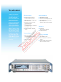
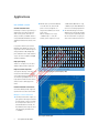
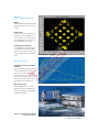
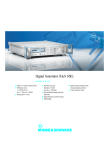
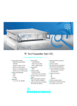
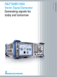
Test Equipment Solutions Datasheet
Test Equipment Solutions Ltd specialise in the second user sale, rental and distribution of
quality test & measurement (T&M) equipment. We stock all major equipment types such as
spectrum analyzers, signal generators, oscilloscopes, power meters, logic analysers etc from
all the major suppliers such as Agilent, Tektronix, Anritsu and Rohde & Schwarz.
We are focused at the professional end of the marketplace, primarily working with customers
for whom high performance, quality and service are key, whilst realising the cost savings that
second user equipment offers. As such, we fully test & refurbish equipment in our in-house,
traceable Lab. Items are supplied with manuals, accessories and typically a full no-quibble 2
year warranty. Our staff have extensive backgrounds in T&M, totalling over 150 years of
combined experience, which enables us to deliver industry-leading service and support. We
endeavour to be customer focused in every way right down to the detail, such as offering free
delivery on sales, covering the cost of warranty returns BOTH ways (plus supplying a loan
unit, if available) and supplying a free business tool with every order.
As well as the headline benefit of cost saving, second user offers shorter lead times, higher
reliability and multivendor solutions. Rental, of course, is ideal for shorter term needs and
offers fast delivery, flexibility, try-before-you-buy, zero capital expenditure, lower risk and off
balance sheet accounting. Both second user and rental improve the key business measure of
Return On Capital Employed.
We are based near Heathrow Airport in the UK from where we supply test equipment
worldwide. Our facility incorporates Sales, Support, Admin, Logistics and our own in-house
Lab.
All products supplied by Test Equipment Solutions include:
- No-quibble parts & labour warranty (we provide transport for UK mainland addresses).
- Free loan equipment during warranty repair, if available.
- Full electrical, mechanical and safety refurbishment in our in-house Lab.
- Certificate of Conformance (calibration available on request).
- Manuals and accessories required for normal operation.
- Free insured delivery to your UK mainland address (sales).
- Support from our team of seasoned Test & Measurement engineers.
- ISO9001 quality assurance.
Test equipment Solutions Ltd
Unit 8 Elder Way
Waterside Drive
Langley
Berkshire
SL3 6EP
T: +44 (0)1753 596000
F: +44 (0)1753 596001
Email: [email protected]
Web: www.TestEquipmentHQ.com
Vector Signal Generator R&S SMV03
Vector modulation in the analog class
◆ Frequency range 9 kHz to 3.3 GHz
◆ I/Q modulator (100 MHz RF bandwidth) with excellent vector accuracy
(f >500 MHz to 3 GHz)
◆ SSB phase noise –128 dBc (1 Hz)
◆ Setting times <10 ms
◆ High level accuracy <0.5 dB
◆ High reliability through electronic
attenuator
◆ Digital frequency and level sweep
◆ AM/FM/ϕM
◆ Optional pulse modulator with
integrated pulse generator
◆ 3-year calibration cycle
The allrounder
The Vector Signal Generator
R&S SMV03 is based on the
successful analog Signal
Generator R&S SML03 and so
features the same excellent
technical characteristics. It
comprises an additional broadband I/Q modulator which is
able to generate any digital
signal in conjunction with an
external I/Q source. The R&S
SMV03 is, therefore, a way of
entering the wide field of automatic test systems as well as
gaining access to applications
like R&D and service. When
used together with the R&S
AMIQ and R&S WinIQSIM™,
the R&S SMV03 can generate
digital signals that meet any
requirement.
2
Vector Signal Generator R&S SMV03
RF characteristics
Analog modulation
◆ Frequency range from 9 kHz to
3.3 GHz with 0.1 Hz resolution
◆ High output level of +13 dBm with a
deviation <0.5 dB
◆ Interruption-free level setting by
electronic attenuator
◆ High spectral purity
(<–122 dBc (1 Hz) at f = 1 GHz and
20 kHz carrier offset)
◆ Frequency and level setting time
<10 ms
◆ AM/FM/ϕM as standard
◆ Simultaneous AM, FM/ϕM, pulse and
vector modulation
◆ Optional pulse modulator with integrated pulse generator (R&S SML-B3)
Dimensions
◆ Compact size
427 mm x 88 mm x 450 mm
◆ Low weight <9.5 kg
Vector modulation
Low cost of ownership
◆ Wide I/Q bandwidth of >50 MHz
(3 dB), 100 MHz RF bandwidth for
f >500 MHz to 3 GHz
◆ High vector accuracy
◆ 3-year calibration cycle
◆ Electronic attenuator for wear-free
operation
◆ Service-friendly (continuous selftest,
access to internal test points)
Applications
Production:
fast, accurate, reliable
Versatility
The R&S SMV03 generates all kinds of
I/Q-modulated signals using the integrated vector modulator. Thanks to its wide I/
Q bandwidth of 50 MHz, the R&S SMV03
is also optimally suited for applications
using high data rates such as WLAN standards. Signals to digital stan-dards can be
easily generated in conjunction with an
external I/Q source like the Modulation
Generator R&S AMIQ (PD 0757.3970)
and the associated R&S WinIQSIM™
simulation software (PD 0757.6940).
The R&S SMV03 therefore optimally
meets production environment requirements.
Dimensions
The compact size (only 2 HU) makes the
R&S SMV03 ideal for use in production
where space is often limited.
Reliability
A signal generator used in production
must feature high reliability. The R&S
SMV03 meets this requirement, for
example, through the use of a completely
wear-free electronic attenuator.
Output level
In production test systems, the signal is
routed to the DUT via switches and cables
which introduce losses. This can be compensated for by the high output power of
the R&S SMV03.
Example: component test
◆ Tests using digital signals are becoming increasingly important for checking the functions of individual components – especially at the component production stage. In this environment, the R&S SMV03's I/Q modulator shows what it can do. Thanks to
its wide signal bandwidth of 50 MHz,
it can generate a great variety of digital signals when an external I/Q source is used.
◆ To obtain reliable information on component quality, high level accuracy
and high output level repeatability are
essential. The R&S SMV03 fully
meets these requirements thanks to a
maximum level uncertainty of <0.5 dB
(at levels >–120 dBm) and high reproducibility.
◆ Extremely short frequency and level
setting times (<10 ms) allow fast
measurements and make the R&S
SMV03 the ideal generator for production testing.
◆ Overshoots that occur when the level
is changed may damage or even destroy the DUT. This cannot happen
with the R&S SMV03 as no
overshoots are produced.
Speed
Speed is essential – especially in production. And this is exactly where the R&S
SMV03 shows what it can do with a frequency and level setting time of <10 ms.
Accuracy
Any measurement uncertainty has two
components: the uncertainty due to the
measuring instrument and that due to the
rest of the test setup. The lower the level
uncertainty of the vector signal generator, the greater the test setup tolerance
that may be allowed. If greater tolerances
can be allowed for the DUT because of
the small level error of the R&S SMV03,
production rejects can be markedly reduced – an advantage that pays off immediately.
I
Q
RF
DUT
Vector Signal Generator R&S SMV03
3
Applications
Versatile modulation modes
Particularly in research, a great variety of
digital signals are used in the development of new systems, which are not
always covered by a standard. Thanks to
its very wideband I/Q modulator, the R&S
SMV03 can handle universal tasks of this
kind.
In conjunction with the optional Pulse
Modulator R&S SML-B3, the vector signal generator can also handle all types of
analog modulation. AM, FM/ϕM and
pulse modulation can be used simultaneously as can vector modulation, FM/ϕM
and pulse modulation.
◆ Minimal spurious, minimal broadband
noise and, above all, excellent SSB
phase noise are prerequisites for
using the R&S SMV03 as an interference source.
With an SSB phase noise of typ.
–128 dBc/Hz (at f = 1 GHz, ∆f =
20 kHz), spurious suppression of typ.
–76 dBc and broadband noise of typ.
–150 dBc (1 Hz), the R&S SMV03 meets
even the most exacting requirements.
◆ The mechanical design of the R&S
SMV03 ensures excellent RF shielding
of its casing. This is particularly important for measurements on highly sensitive receivers with built-in antenna.
2
0
Response (dB)
Lab and R&D: versatile
–2
–4
–6
High spectral purity
Thanks to its low phase noise, the R&S
SMV03 is ideally suited to replace LOs.
High and accurate output level
The high level accuracy of the Vector Signal Generator R&S SMV03 is a prerequisite for highly accurate measurements on
sensitive analog and digital receivers. Its
high output level makes the R&S SMV03
an ideal source for driving high-level
mixers.
–8
–10
–100 –90
–80 –70
–60
–50
–20
–10
0
10
20
Frequency response of I/Q modulator (carrier frequency 1 GHz)
Example: receiver measurements
◆ Sensitivity measurements require a signal generator with high level accuracy. High accuracy is even more critical
at low output levels. Thanks to its sophisticated calibration methods, the
R&S SMV03 features high level accuracy (uncertainty <0.5 dB at levels
>–120 dBm).
Vector diagram of QPSK signals
Vector Signal Generator R&S SMV03
–30
30
Frequency offset from carrier (MHz)
Excellent modulation characteristics
As the R&S SMV03 provides high-linearity FM, it can be used as a precise VCO.
4
–40
40
50
60
70
80
90
100
Servicing:
robust, compact, lightweight
Mobility
The R&S SMV03 is lightweight (<9.5 kg)
and compact and therefore very easy to
transport.
Flexible control
In service environments, an IEC/IEEE bus
interface is not always available to control the generator. This is not a problem as
the R&S SMV03 can also be controlled
via a standard RS-232-C interface.
Protection against overvoltage
The integrated overvoltage protection of
the RF output protects the R&S SMV03
against very high external voltages such
as may occur during transceiver measurements.
Constellation diagram of WCDMA signal in 3GPP TDD mode
EMS measurements
Interruption-free level setting without
overshoots
EMS measurements require interruptionfree level setting which should also be
overshoot-free. The R&S SMV03 does not
produce any overshoots – even at setting
times <10 ms. Furthermore, it has a wide
dynamic range of typ. 30 dB over which
level adjustment is interruption-free.
Wide frequency range
The R&S SMV03 features a lower frequency limit of 9 kHz as standard and so
fully covers the frequency range required
for EMC measurements.
Typical SSB phase noise at 1 GHz (with OCXO option R&S SML-B1)
Module test with R&S SMV03, R&S AMIQ and
Spectrum Analyzer R&S FSP
Vector Signal Generator R&S SMV03
5
Reference source
–115
–120
Phase noise/dBc(1 Hz)
The R&S SMV03 allows selection of the
mode of frequency generation. In the
extended divider range mode, the RF signal is generated by frequency division.
The excellent values obtained in this
mode for SSB phase noise are comparable to those from the high-grade crystal
oscillators normally used as reference
sources from 10 MHz to 30 MHz.
–125
–130
–135
–140
–145
Compared to crystal oscillators, the R&S
SMV03 has the following benefits:
◆ Frequency can be set in 0.1 Hz steps
and synchronized to an external reference
◆ All functions can be remotely controlled via the IEC/IEEE bus or serial interface
EasyWheel
◆ One-hand operation with
EasyWheel
◆ All settings simple and
self-explanatory
◆ High-contrast LCD
◆ User-assignable menu keys
◆ Online help including IEC/IEEE bus
commands
–150
10
50
100
500
Offset from carrier
SSB phase noise, typical values
1 Hz
–95 dB
10 Hz
–120 dB
100 Hz
–130 dB
1 kHz
–138 dB
10 kHz
–148 dB
SSB phase noise at 9.5 MHz output frequency, extended divider range activated, 1 Hz measurement
bandwidth
Certified Quality System
ISO 9001
DQS REG. NO 1954
Certified Environmental System
ISO 14001
REG. NO 1954
Simply select the desired menu with the spinwheel and click the button to open the submenu
6
Vector Signal Generator R&S SMV03
3300
Typical SSB phase noise versus carrier frequency (carrier offset 20 kHz); dashed line: extended divider
range mode
Turn
Click
1000
Frequency/MHz
Specifications
Specifications apply under the following conditions:
30 minutes warmup time at ambient temperature, specified environmental conditions met, calibration cycle adhered to, and total calibration performed.
Data designated “nominal” are design parameters and are not tested.
Data designated “overrange” are not warranted.
.
Frequency
R&S SMV03
I/Q modulation off
I/Q modulation on
9 kHz to 3.3 GHz
5 MHz to 3.3 GHz
Resolution
0.1 Hz
Characteristic impedance
50 Ω
SWR
100 kHz to 1.5 GHz
f >1.5 GHz
1.6
2.3
Setting time (IEC/IEEE bus),
f >100 kHz
<10 ms, 5 ms typ.
Interruption-free level setting5)
(for f >100 kHz)
I/Q modulation off
I/Q modulation on
20 dB, overrange 30 dB
15 dB, overrange 20 dB
safeguards unit against externally
applied RF power and DC voltage
(50 Ω source)
Overvoltage protection
Setting time (for an offset of <1x10⁻⁷ or
<90 Hz for f ≤76 MHz) after IEC/IEEE
bus delimiter
<10 ms
I/Q modulation off
<12 ms
I/Q modulation on
Max. permissible RF power
f ≤2.2 GHz
f >2.2 GHz
50 W
25 W
Max. permissible DC voltage
35 V
Vector modulation
Reference frequency
Standard
Aging (after 30 days of operation)
−6
<1 x 10 /year
Option R&S SML-B1
<1 x 10⁻⁷/year
−10
<5 x 10
−6
Temperature effect (0°C to 55°C)
<1 x 10
<2 x 10
Output for internal reference
Frequency
Output voltage, V rms, sinewave
Source impedance
10 MHz
>0.5 V into 50 Ω
50 Ω
Input for external reference
Frequency
Permissible frequency drift
Input voltage, V rms, sinewave
Input impedance
10 MHz
5 x 10⁻⁶
0.5 V to 2 V into 50 Ω
50 Ω
/day
−8
Spectral purity
Spurious signals
Harmonics1) (for f >100 kHz)
Subharmonics
f ≤1.1 GHz
f >1.1 GHz
Nonharmonics
(carrier offset >10 kHz)
f ≤1.1 GHz
f >1.1 GHz to 2.2 GHz
f >2.2 GHz to 3.3 GHz
<–30 dBc at levels ≤+8 dBm
–
<–50 dBc
<–70 dBc
<–64 dBc
<–58 dBc
Broadband noise2) 3) (f = 1 GHz,
carrier offset >2 MHz, 1 Hz bandwidth) <−135 dBc, −140 dBc typ.
SSB phase noise (f = 1 GHz,
20 kHz carrier offset, 1 Hz bandwidth) <−122 dBc, −128 dBc typ.
Spurious FM, rms (f = 1 GHz)
0.3 kHz to 3 kHz
0.03 kHz to 20 kHz
<4 Hz, 1 Hz typ.
<10 Hz, 3 Hz typ.
Spurious AM, rms
0.03 kHz to 20 kHz
<0.02%
Level
−140 dBm to +13 dBm 2) 4)
(overrange +19 dBm)
Range
Resolution
external DC
I and Q modulation inputs
Input impedance
SWR (DC to 30 MHz)
Input voltage for full-scale level
50 Ω
<1.2
2
2
I + Q = 0,. 5V
(1 V EMF with 50 Ω source)
Static error vector6),
Level <+8 dBm
Rms value
f <2.6 GHz
f >2.6 GHz to f=3 GHz
Peak value
f <2.6 GHz
f >2.6 GHz to f=3 GHz
<0.5%
<0.7%
<1%
<1.4%
Modulation frequency response
f >500 MHz to 3 GHz
DC to 5 MHz
DC to 50 MHz
f <500 MHz and f >3 GHz7)
DC to 5 MHz
DC to 30 MHz
<0.4 dB
<3 dB
<0.4 dB
<3 dB
Residual carrier at 0 V input voltage
referred to max. input voltage
<–45 dBc (at f=5 MHz to 3 GHz)
I/Q imbalance
Carrier leakage
Setting range
Resolution
I≠Q
Setting range
Resolution
Quadrature offset
Setting range
Resolution
0% to 50%
0.5%
–12% to +12%
0.1%
–10° to +10°
0.1°
0.1 dB
<0.5 dB
<0.9 dB
Internal modulation generator
2) 3)
Frequency response at 0 dBm
100 kHz to ≤2 GHz
f >2 GHz
Operating mode
Adjacent-channel leakage ratio (ACLR)
WCDMA 3GPP FDD
(f = 2.14 GHz)
Test model 1 (64 DPCHs)
nom. >60 dB, 62 dB typ.
Offset 5 MHz
nom. >64 dB, 66 dB typ.
Offset 10 MHz
2) 3)
Level accuracy
(level >−120 dBm)
100 kHz to ≤2 GHz
f >2 GHz
Additional level inaccuracy in case of
vector modulation (ALC OFF), referred
<0.3 dB
to CW mode
<0.7 dB
<1.0 dB
Frequency range
Resolution
0.1 Hz to 1 MHz
0.1 Hz
Frequency accuracy
as for reference frequency +
2.4 x 10⁻³ Hz
Vector Signal Generator R&S SMV03
7
Frequency response
(up to 500 kHz, level >100 mV)
<0.5 dB
Carrier frequency offset at FM DC
THD (up to 100 kHz, level 4 V,
RL = 600 Ω)
<0.1%
Open-circuit voltage Vp (LF connector) 1 mV to 4 V
Resolution
1 mV
Setting accuracy (at 1 kHz)
1% of Vp + 1 mV
Output impedance
approx. 10 Ω
Frequency setting time (after reception
<10 ms
of last IEC/IEEE bus character)
Simultaneous modulation
AM, FM/ϕM and pulse modulation or
vector modulation, FM/ϕM and pulse
modulation
Amplitude modulation8)
Operating modes
internal, external AC/DC,
internal/external two-tone
Modulation depth
0% to 100%
settable modulation depth continuously
decreasing between +7 dBm and
+13 dBm9) while adhering to AM specifications; a status message is output
when the modulation depth is too high
Resolution
0.1%
Setting accuracy at 1 kHz
(m <80%)10)
<4% of reading +1%
AM distortion at 1 kHz
m = 30%
m = 80%
<1%
<2%
Modulation frequency range
(<3 dB)
DC/10 Hz to 50 kHz
Incidental ϕM at AM (30%),
AF = 1 kHz
Modulation input EXT
Input impedance
Input voltage Vp for set
modulation depth
<0.2 rad
>100 kΩ
1V
Frequency modulation
Operating modes
Frequency deviation
9 kHz to 76 MHz
>76 MHz to 151.3125 MHz
>151.3125 MHz to 302.625 MHz
>302.625 MHz to 605.25 MHz
>605.25 MHz to 1.2105 GHz
>1.2105 GHz to 1.818 GHz
>1.818 GHz to 2.655 GHz
>2.655 GHz to 3.300 GHz
internal, external AC/DC,
internal/external two-tone
0 Hz to 1 MHz
0 Hz to 125 kHz
0 Hz to 250 kHz
0 Hz to 500 kHz
0 Hz to 1 MHz
0 Hz to 2 MHz
0 Hz to 3 MHz
0 Hz to 4 MHz
Resolution
<1% of set deviation,
minimum 10 Hz
Setting accuracy (at AF = 1 kHz)
<4% of reading + 20 Hz
FM distortion (at AF = 1 kHz and
50% of max. deviation)
<0.2%, 0.1% typ.
Modulation frequency range
(<3 dB)
Standard
Wide
DC to 100 kHz
10 Hz to 500 kHz
Incidental AM (at AF = 1 kHz,
f >10 MHz, 40 kHz deviation)
<0.1%
Stereo modulation at 40 kHz useful
deviation, AF = 1 kHz,
RF = 87 MHz to 108 MHz
Crosstalk
S/N ratio unweighted, rms
S/N ratio weighted, rms
Distortion
0.1% typ. of set deviation
Modulation input EXT
Input impedance
Input voltage Vp for set deviation
(nominal value)
>100 kΩ
1V
Phase modulation
Operating modes
internal, external AC/DC,
internal/external two-tone
Phase deviation11)
9 kHz to 76 MHz
>76 MHz to 151.3125 MHz
>151.3125 MHz to 302.625 MHz
>302.625 MHz to 605.25 MHz
>605.25 MHz to 1.2105 GHz
>1.2105 GHz to 1.818 GHz
>1.818 GHz to 2.655 GHz
>2.655 GHz to 3.300 GHz
0 rad to 10 (2) rad
0 rad to 1.25 (0.25) rad
0 rad to 2.5 (0.5) rad
0 rad to 5 (1) rad
0 rad to 10 (2) rad
0 rad to 20 (4) rad
0 rad to 30 (6) rad
0 rad to 40 (8) rad
Resolution
<1%, min. 0.001 rad
Setting accuracy at AF = 1 kHz
<4% of reading + 0.02 rad
Phase distortion (at AF = 1 kHz and
50% of maximum deviation)
<0.2%, 0.1% typ.
Modulation frequency range (–3 dB)
Standard
Wide
DC to 100 kHz
10 Hz to 500 kHz
Modulation inputs EXT
Input impedance
Input voltage Vp for set deviation
(nominal value)
>100 kΩ
1V
Pulse modulation (with option R&S SML-B3)
Operating modes
internal, external
On/off ratio
>80 dB
Rise/fall time (10%/90%)
<20 ns, 10 ns typ.
Pulse repetition frequency
0 Hz to 2.5 MHz
Pulse delay
50 ns typ.
Video crosstalk (Vp)
<30 mV
Modulation input PULSE
Input level
Input impedance
TTL level (HCT)
10 kΩ or 50 Ω, selectable with internal
link
Pulse generator (with option R&S SML-B3)
Operating modes
automatic, externally triggered, external
gate mode, single pulse, double pulse,
delayed pulse (externally triggered)
Active trigger edge
positive or negative
Pulse period
Resolution
Accuracy
100 ns to 85 s
5 digits, min. 20 ns
<1 x 10⁻⁴
Pulse width
Resolution
Accuracy
20 ns to 1 s
4 digits, min. 20 ns
<1 x 10⁻⁴ + 3 ns
Pulse delay
Resolution
Accuracy
20 ns to 1 s
4 digits, min. 20 ns
<1 x 10⁻⁴ + 3 ns
Double-pulse spacing
Resolution
Accuracy
20 ns to 1 s
4 digits, min. 20 ns
<1 x 10⁻⁴ + 3 ns
Trigger delay
50 ns typ.
Jitter
<10 ns
PULSE/VIDEO output
TTL signal (RL ≥50 Ω)
>50 dB
>70 dB
>70 dB
<0.2%, 0.1% typ.
Vector Signal Generator R&S SMV03
8
Sweep
RF sweep, AF sweep
Operating modes
Sweep range
Step width (lin)
Step width (log)
Level sweep
Operating modes
Sweep range
Step width (log)
digital in discrete steps
Electromagnetic compatibility
meets EN 55011 and EN 61326-1
(EMC directive of EU)
automatic, single-shot, manually or externally triggered, linear or logarithmic
user-selectable
user-selectable
0.01% to 100%
Immunity to radiated interference
10 V/m
Power supply
100 V to 120 V (AC), 50 Hz to 400 Hz,
200 V to 240 V (AC), 50 Hz to 60 Hz,
autoranging, max. 250 VA
Safety
meets DIN EN 61010-1, IEC 1010-1,
UL 3111-1, CSA 22.2 No. 1010-1
Dimensions (W x H x D)
427 mm x 88 mm x 450 mm
Weight
9.5 kg when fully equipped
automatic, single-shot, manually or
externally triggered, logarithmic
user-selectable
user-selectable
Step time
Resolution
10 ms to 1 s
0.1 ms
Trigger input
Input level
Input impedance
TTL (HCT)
10 kΩ (pull-up)
1)
2)
3)
4)
5)
6)
Memory for device settings
Number of storable settings
100
Remote control
7)
8)
9)
10)
With option R&S SML-B3 only for f > 20 MHz.
With attenuator mode auto.
Temperature range 20°C to 30°C.
–140 dBm to 11 dBm at f ≤5 MHz, f >3 GHz.
With attenuator mode fixed.
After 1 hour warmup and recalibration within 4 hours of operation after
temperature variations <5°C.
The modulation bandwidth continuously decreases upon approaching 5 MHz or. 3.3 GHz.
With attenuator mode auto, f ≥100 kHz.
+5 dBm to +11 dBm at f ≤5 MHz, f >3 GHz.
With option R&S SML-B3 only for f >10 MHz.
Values in brackets apply to wide modulation bandwidth.
System
IEC 60625 (IEEE 488) and RS-232-C
Command set
SCPI 1995.0
Connector
Amphenol, 24-pin and 9-pin
IEC/IEEE bus address
0 to 30
Ordering information
Interface functions
SH1, AH1, T6, L4, SR1, RL1, PP1, DC1,
DT1, C0
Vector Signal Generator
Rated temperature range
0°C to 55°C;
meets IEC 68-2-1 and IEC 68-2-2
Storage temperature range
−40°C to +70°C
Options
Reference Oscillator OCXO
Pulse Modulator
Stereo /RDS Coder
Rear Connectors for AF, RF
General data
Climatic resistance
Damp heat
Mechanical resistance
Vibration, sinusoidal
Vibration, random
Shock
95% relative humidity at +25°C/
+40°C cyclically; meets IEC 60068
5 Hz to 150 Hz, max. 2 g at 55 Hz,
max. 0.5 g between 55 Hz and
150 Hz, meets IEC 60068, IEC 61010
and MIL-T-28800D, class 5
10 Hz to 300 Hz,
acceleration 1.2 g (rms)
40 g shock spectrum,
meets MIL-STD-810D and
MIL-T-28800D, class 3/5
11)
R&S SMV03
Accessories supplied
Recommended extras
Service Kit
19“ Rack Adapter
Transport Bag
Service Manual, Modules
1)
1147.7509.13
power cable,
user manual
R&S SML-B1
R&S SML-B3
R&S SML-B5
R&S SML-B19
1090.5790.02
1090.5403.021)
1147.8805.02
1090.5303.021)
R&S SML-Z2
R&S ZZA-211
R&S ZZT-214
1090.5203.02
1096.3260.00
1109.5119.00
1090.3123.24
Factory-fitted only.
Vector Signal Generator R&S SMV03
9
1102 (U bb)
Printed in Germany
PD 0757.7175.22 ⋅ Vector Signal Generator R&S SMV03 ⋅ Trade names are trademarks of the owners ⋅ Subject to change ⋅ Data without tolerances: typical values
ROHDE&SCHWARZ GmbH & Co. KG ⋅ Mühldorfstraße 15 ⋅ 81671 München ⋅ Germany ⋅ P.O.B. 8014 69 ⋅ 81614 München ⋅ Germany ⋅ Telephone +49 89 4129-0
www.rohde-schwarz.com ⋅ Customer Support: Telephone +49 1805124242, Fax +49 89 4129-13777, E-mail: [email protected]