1
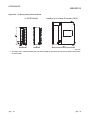
I/O Module Type Building Block
User's Manual
SAFETY PRECAUTIONS
(Read these precautions before using this product.)
Before using this product, please read this manual and the relevant manuals carefully and pay full
attention to safety to handle the product correctly.
The precautions given in this manual are concerned with this product only. For the safety precautions of
the programmable controller system, refer to the user’s manual for the CPU module used.
In this manual, the safety precautions are classified into two levels: " ! WARNING" and " ! CAUTION".
! WARNING
Indicates that incorrect handling may cause hazardous conditions,
resulting in death or severe injury.
! CAUTION
Indicates that incorrect handling may cause hazardous conditions,
resulting in minor or moderate injury or property damage.
Under some circumstances, failure to observe the precautions given under " ! CAUTION" may lead to
serious consequences.
Observe the precautions of both levels because they are important for personal and system safety.
Make sure that the end users read this manual and then keep the manual in a safe place for future
reference.
[Design Precautions]
!
WARNING
• Configure safety circuits external to the programmable controller to ensure that the entire system
operates safely even when a fault occurs in the external power supply or the programmable
controller. Failure to do so may result in an accident due to an incorrect output or malfunction.
(1) Configure external safety circuits, such as an emergency stop circuit, protection circuit, and
protective interlock circuit for forward/reverse operation or upper/lower limit positioning.
(2) When the programmable controller detects an abnormal condition, it stops the operation and
all outputs are:
(a) Turned off if the overcurrent or overvoltage protection of the power supply module is
activated.
(b) Held or turned off according to the parameter setting if the self-diagnostic function of the
CPU module detects an error such as a watchdog timer error.
Note, however, that AnS series modules on the system turn off all outputs in both cases.
All outputs may turn on if an error occurs in a part, such as an I/O control part, where the
CPU module cannot detect any error. To ensure safety operation in such a case, provide a
safety mechanism or a fail-safe circuit external to the programmable controller. For a failsafe circuit example, refer to the user’s manual for the CPU module used.
(3) Outputs may remain on or off due to a failure of an output module relay or transistor.
Configure an external circuit for monitoring output signals that could cause a serious
accident.
A-1
A-1
[Design Precautions]
!
WARNING
• In an output module, when a load current exceeding the rated current or an overcurrent caused
by a load short-circuit flows for a long time, it may cause smoke and fire. To prevent this,
configure an external safety circuit, such as a fuse.
• Configure a circuit so that the programmable controller is turned on first and then the external
power supply.
If the external power supply is turned on first, an accident may occur due to an incorrect output
or malfunction.
• For the operating status of each station after a communication failure, refer to relevant manuals
for each network.
Incorrect output or malfunction due to a communication failure may result in an accident.
• When changing data of the running programmable controller from a peripheral connected to the
CPU module or from a personal computer connected to an intelligent function module, configure
an interlock circuit in the sequence program to ensure that the entire system will always operate
safely.
For other controls to a running programmable controller (such as program modification or
operating status change), read relevant manuals carefully and ensure the safety before the
operation.
Especially, in the case of a control from an external device to a remote programmable controller,
immediate action cannot be taken for a problem on the programmable controller due to a
communication failure.
To prevent this, configure an interlock circuit in the sequence program, and determine corrective
actions to be taken between the external device and CPU module in case of a communication
failure.
!
CAUTION
• Do not install the control lines or communication cables together with the main circuit lines or
power cables.
Keep a distance of 100mm or more between them.
Failure to do so may result in malfunction due to noise.
• When a device such as a lamp, heater, or solenoid valve is controlled through an output module,
a large current (approximately ten times greater than normal) may flow when the output is
turned from off to on. Take measures such as replacing the module with one having a sufficient
current rating.
A-2
A-2
[Installation Precautions]
!
CAUTION
• Use the programmable controller in an environment that meets the general specifications in the
user’s manual for the CPU module used.
Failure to do so may result in electric shock, fire, malfunction, or damage to or deterioration of
the product.
• To mount the module, while pressing the module mounting lever located in the lower part of the
module, fully insert the module fixing projection(s) in the hole(s) in the base unit and press the
module until it snaps into place.
Incorrect interconnection may cause malfunction, failure, or drop of the module.
When using the programmable controller in an environment of frequent vibrations, fix the
module with a screw.
Tighten the screw within the specified torque range.
Undertightening can cause drop of the screw, short circuit or malfunction.
Overtightening can damage the screw and/or module, resulting in drop, short circuit, or
malfunction.
• When using an extension cable, connect it to the extension cable connector of the base unit
securely.
Check the connection for looseness.
Poor contact may cause incorrect input or output.
• When using a memory card, fully insert it into the memory card slot.
Check that it is inserted completely.
Poor contact may cause malfunction.
• Shut off the external power supply for the system in all phases before mounting or removing the
module.
Failure to do so may result in damage to the product.
• Do not touch the module during turning on electricity and immediately after power supply
interception. There is fear of a burn.
• Do not directly touch any conductive parts and electronic components of the module.
Doing so can cause malfunction or failure of the module.
[Wiring Precautions]
!
WARNING
• Shut off the external power supply for the system in all phases before wiring.
Failure to do so may result in electric shock or damage to the product.
• After wiring, attach the included terminal cover to the module before turning it on for operation.
Failure to do so may result in electric shock.
A-3
A-3
[Wiring Precautions]
!
CAUTION
• Individually ground the FG and LG terminals of the programmable controller with a ground
resistance of 100 Ω or less.
Failure to do so may result in electric shock or malfunction.
• Check the rated voltage and terminal layout before wiring to the module, and connect the cables
correctly.
Connecting a power supply with a different voltage rating or incorrect wiring may cause a fire or
failure.
• Connectors for external devices must be crimped or pressed with the tool specified by the
manufacturer, or must be correctly soldered.
Incomplete connections may cause short circuit, fire, or malfunction.
• Tighten the terminal screw within the specified torque range.
Undertightening can cause short circuit, fire, or malfunction.
Overtightening can damage the screw and/or module, resulting in drop, short circuit, or
malfunction.
• Prevent foreign matter such as dust or wire chips from entering the module.
Such foreign matter can cause a fire, failure, or malfunction.
• A protective film is attached to the top of the module to prevent foreign matter, such as wire
chips, from entering the module during wiring.
Do not remove the film during wiring.
Remove it for heat dissipation before system operation.
• Mitsubishi programmable controllers must be installed in control panels.
Connect the main power supply to the power supply module in the control panel through a relay
terminal block.
Wiring and replacement of a power supply module must be performed by qualified maintenance
personnel with knowledge of protection against electric shock.
(For wiring methods, refer to the QCPU User's Manual (Hardware Design, Maintenance and
Inspection).)
A-4
A-4
[Startup and Maintenance Precautions]
!
WARNING
• Do not touch any terminal while power is on.
Doing so will cause electric shock.
• Correctly connect the battery connector.
Do not charge, disassemble, heat, short-circuit, or solder the battery, or throw it into the fire.
Doing so will cause the battery to produce heat, explode, or ignite, resulting in injury and fire.
• Shut off the external power supply for the system in all phases before cleaning the module or
retightening the terminal screws or module fixing screws.
Failure to do so may result in electric shock.
Undertightening the terminal screws can cause short circuit or malfunction.
Overtightening can damage the screw and/or module, resulting in drop, short circuit, or
malfunction.
A-5
A-5
[Startup and Maintenance Precautions]
!
CAUTION
• Before performing online operations (especially, program modification, forced output, and
operating status change) for the running CPU module from the peripheral device connected,
read relevant manuals carefully and ensure the safety.
Improper operation may damage machines or cause accidents.
• Do not disassemble or modify the modules.
Doing so may cause failure, malfunction, injury, or a fire.
• Shut off the external power supply for the system in all phases before mounting or removing the
module.
Failure to do so may cause the module to fail or malfunction.
• After the first use of the product, do not mount/remove the module to/from the base unit, and the
terminal block to/from the module more than 50 times (IEC 61131-2 compliant) respectively.
Exceeding the limit may cause malfunction.
• Before handling the module, touch a grounded metal object to discharge the static electricity
from the human body.
Failure to do so may cause the module to fail or malfunction.
[Disposal Precautions]
!
CAUTION
• When disposing of this product, treat it as industrial waste.
A-6
A-6
• CONDITIONS OF USE FOR THE PRODUCT •
(1) Mitsubishi programmable controller ("the PRODUCT") shall be used in conditions;
i) where any problem, fault or failure occurring in the PRODUCT, if any, shall not lead to any major or
serious accident; and
ii) where the backup and fail-safe function are systematically or automatically provided outside of the
PRODUCT for the case of any problem, fault or failure occurring in the PRODUCT.
(2) The PRODUCT has been designed and manufactured for the purpose of being used in general
industries.
MITSUBISHI SHALL HAVE NO RESPONSIBILITY OR LIABILITY (INCLUDING, BUT NOT LIMITED
TO ANY AND ALL RESPONSIBILITY OR LIABILITY BASED ON CONTRACT, WARRANTY, TORT,
PRODUCT LIABILITY) FOR ANY INJURY OR DEATH TO PERSONS OR LOSS OR DAMAGE TO
PROPERTY CAUSED BY the PRODUCT THAT ARE OPERATED OR USED IN APPLICATION NOT
INTENDED OR EXCLUDED BY INSTRUCTIONS, PRECAUTIONS, OR WARNING CONTAINED IN
MITSUBISHI'S USER, INSTRUCTION AND/OR SAFETY MANUALS, TECHNICAL BULLETINS AND
GUIDELINES FOR the PRODUCT.
("Prohibited Application")
Prohibited Applications include, but not limited to, the use of the PRODUCT in;
• Nuclear Power Plants and any other power plants operated by Power companies, and/or any other
cases in which the public could be affected if any problem or fault occurs in the PRODUCT.
• Railway companies or Public service purposes, and/or any other cases in which establishment of a
special quality assurance system is required by the Purchaser or End User.
• Aircraft or Aerospace, Medical applications, Train equipment, transport equipment such as Elevator
and Escalator, Incineration and Fuel devices, Vehicles, Manned transportation, Equipment for
Recreation and Amusement, and Safety devices, handling of Nuclear or Hazardous Materials or
Chemicals, Mining and Drilling, and/or other applications where there is a significant risk of injury to
the public or property.
Notwithstanding the above, restrictions Mitsubishi may in its sole discretion, authorize use of the
PRODUCT in one or more of the Prohibited Applications, provided that the usage of the PRODUCT is
limited only for the specific applications agreed to by Mitsubishi and provided further that no special
quality assurance or fail-safe, redundant or other safety features which exceed the general
specifications of the PRODUCTs are required. For details, please contact the Mitsubishi
representative in your region.
A-7
A-7
REVISIONS
The manual number is given on the bottom left of the back cover.
Print Date
Dec., 1999
Feb., 2000
Manual Number
Revision
SH (NA)-080042-A First edition
SH (NA)-080042-B Addition model
QH42P, QX48Y57, QX70, QX71, QX72, QY18A
Addition
Chapter 4
Partial correction
Section 1.2, Chapter 5, 8.1
Chapters 4 to 8 (changed into Chapters 5 to 9)
Apr., 2000
SH (NA)-080042-C
Deletion
QY18A
Jul., 2000
SH (NA)-080042-D
Addition model
QX28, QX40-S1, QY18A, QY22, QI60
Addition
Chapter 5
Partial correction
Section 1.2
Chapters 5 to 9 (changed into Chapters 6 to 10)
Nov., 2000
SH (NA)-080042-E
Addition model
QY70, QY71
Addition
Section 1.3
Partial correction
CONTENTS, Section 3.3, 5.1
Jan., 2001
SH (NA)-080042-F
Addition model
QY68A
Addition
Section 10.2
Partial correction
CONTENTS, Section 1.2, 3.3, 5.1, Chapters 7
Mar., 2001
SH (NA)-080042-G
Partial correction
Section 2.4, 8.1
Jul., 2001
SH (NA)-080042-H
Addition model
Q6TE-18S
Addition
Chapter 9, APP 1.3
Partial correction
CONTENTS, Section 2.1, 2.2, 2.4, 5.1
Chapters 9 to 10 (changed into Chapters 10 to 11)
Jul., 2002
A-8
SH (NA)-080042-I
Addition model
QX41-S1, QX42-S1, A6CON4
A-8
Print Date
Manual Number
Mar., 2003
SH (NA)-080042-J
Addition model
QX82
May, 2003
SH (NA)-080042-K
Partial correction
Section 1.2, 2.2
May, 2003
SH (NA)-080042-L
Addition model
QX82-S1
Revision
Partial correction
Section 1.2, 3.3
Addition
Section 2.15
Jul., 2004
SH (NA)-080042-M
Partial correction
Section 1.2, 2.1 to 2.15, 3.1 to 3.12, 4.1, 4.2, 5.1, 8.1, 8.2.1, 8.2.2, 10
Jul., 2005
SH (NA)-080042-N
Partial correction
SAFETY PRECAUTIONS, Section 3.3
Addition
Appendix 1.3
Apr., 2006
SH (NA)-080042-O
Partial correction
SAFETY PRECAUTIONS, Section 4.1, Chapter 6
Sep., 2006
SH (NA)-080042-P
Partial correction
Section 11.1, 11.2, Appendix 1.2, 1.3
Oct., 2006
SH (NA)-080042-Q
Addition model
QX50
Partial correction
SAFETY PRECAUTIONS, Section 2.10 to 2.16, 3.4 to 3.12, 4.1, 4.2
Addition
Section 2.9
Sep., 2007
SH (NA)-080042-R
Addition model
QX41Y41P
Partial correction
Section 1.2, 1.3.3, 2.1 to 2.16, 3.1 to 3.12, 4.1, 4.3, 5.1, 7.1, 8.1, Chapter
10, Section 11.1, 11.2, Appendix 1.2
Addition
Section 4.2
Jun., 2008
SH (NA)-080042-S
Addition model
QX10-TS, QX40-TS, QX80-TS, QY10-TS, QY40P-TS, QY80-TS
Partial correction
Section 1.2, 2.3 to 2.19, 3.3 to 3.15, 9.2, Chapter 10
Addition
Section 2.2, 2.6, 2.16, 3.2, 3.6, 3.14, 9.1, 9.3
A-9
A-9
Print Date
Manual Number
Oct., 2008
SH (NA)-080042-T
Revision
Addition model
QX40-H, QX70-H, QX80-H, QX90-H
Partial correction
Section 1.2.5, 1.3.1, 2.8 to 2.23, 9.2, Chapter 10
Addition
Section 2.7, 2.14, 2.19, 2.23
Apr., 2009
SH (NA)-080042-U
Addition model
QX41-S2, QX81-S2
Partial correction
Section 2.7, 2.11 to 2.25, 5.1, 8.1
Addition
May, 2010
Section 2.10, 2.22
SH (NA)-080042-V External connections are reviewed according to IEC 60617.
Addition model
QY82P
Partial correction
SAFETY PRECAUTIONS, Section 1.1, 1.2, Chapter 2 to 4, Chapter 7,
Section 8.1, Chapter 10, Section 11.1, 11.2, Appendix 1.1
Addition
CONDITIONS OF USE FOR THE PRODUCT, Section 3.16
Jul., 2011
SH (NA)-080042-W
Addition model
Q6TE-18SN
Partial correction
Section 1.2.1, 1.2.2, 1.2.3, 1.2.6, 3.11, Chapter 7, Section 9.1, 9.2,
Chapter 10, Section 11.2, Appendix 1.3
Mar., 2012
SH (NA)-080042-X
Addition model
QY41H
Partial correction
Section 1.2.2, 2.3, 3.8 to 3.17, Chapter 7, Section 8.1
Addition
Section 3.7
Jun., 2013
SH (NA)-080042-Y
Partial correction
Section 1.2.1, 1.3.1, 2.7, 2.15, 2.20, 2.25, 11.2
Dec., 2013
SH (NA)-080042-Z
Partial correction
Section 2.8, 2.9, 2.10, 2.11, 2.12, 2.16, 2.17, 2.21, 2.22, 2.23, 2.24, 3.7,
3.8, 3.9, 3.13, 3.16, 3.17, 4.1, 4.2, Chapter 7, Appendix 1.2
Oct., 2014 SH (NA)-080042-AA Partial correction
SAFETY PRECAUTIONS, Section 1.2.2, 3.4, 9.2, 11.2
A - 10
A - 10
Print Date
Sep.,2015
Manual Number
Revision
SH (NA)-080042-AB Partial correction
Section 1.2.6, Chapter 2, Chapter 3, Section 5.1, Chapter 6, Section
8.1, Section 9.1, Appendix 1.1, Appendix 1.2, Appendix 1.3, Appendix
1.4
Japanese Manual Version SH-080024-AC
This manual confers no industrial property rights or any rights of any other kind, nor does it confer any patent licenses.
Mitsubishi Electric Corporation cannot be held responsible for any problems involving industrial property rights which
may occur as a result of using the contents noted in this manual.
1999 MITSUBISHI ELECTRIC CORPORATION
A - 11
A - 11
INTRODUCTION
Thank you for purchasing the Mitsubishi MELSEC-Q series programmable controllers.
Before using this product, please read this manual carefully and develop familiarity with the functions and
performance of the MELSEC-Q series programmable controller to handle the product correctly.
CONTENTS
SAFETY PRECAUTIONS .............................................................................................................................A- 1
CONDITIONS OF USE FOR THE PRODUCT ............................................................................................A- 7
REVISIONS ...................................................................................................................................................A- 8
INTRODUCTION...........................................................................................................................................A- 12
CONTENTS ...................................................................................................................................................A- 12
ABOUT MANUALS .......................................................................................................................................A- 15
COMPLIANCE WITH EMC AND LOW VOLTAGE DIRECTIVES ..............................................................A- 15
1. GENERAL SPECIFICATIONS AND PRECAUTIONS FOR USE
1- 1 to 1- 20
1.1 General Specifications ............................................................................................................................ 1- 1
1.2 Precautions for Use ................................................................................................................................ 1- 1
1.2.1 Input module ...................................................................................................................................... 1- 1
1.2.2 Output module ................................................................................................................................... 1- 3
1.2.3 I/O combined module ........................................................................................................................ 1-13
1.2.4 I/O module with protection function .................................................................................................. 1-14
1.2.5 Interrupt module ................................................................................................................................ 1-15
1.2.6 Installation and wiring ........................................................................................................................ 1-15
1.3 Various Settings for I/O Module.............................................................................................................. 1-16
1.3.1 Setting of I/O response time ............................................................................................................. 1-16
1.3.2 Setting of error-time output mode ..................................................................................................... 1-19
1.3.3 Switch setting of interrupt module..................................................................................................... 1-20
2. INPUT MODULE SPECIFICATIONS
2- 1 to 2- 36
2.1 QX10 AC Input Module ........................................................................................................................... 2- 1
2.2 QX10-TS AC Input Module ..................................................................................................................... 2- 2
2.3 QX28 AC Input Module ........................................................................................................................... 2- 3
2.4 QX40 DC Input Module (Positive Common Type) ................................................................................. 2- 4
2.5 QX40-S1 DC Input Module (Positive Common Type) ........................................................................... 2- 5
2.6 QX40-TS DC Input Module (Positive Common Type) .......................................................................... 2- 6
2.7 QX40H DC High-Speed Input Module (Positive Common Type) ........................................................ 2- 7
2.8 QX41 DC Input Module (Positive Common Type) ................................................................................. 2- 9
2.9 QX41-S1 DC Input Module (Positive Common Type) ........................................................................... 2-10
2.10 QX41-S2 DC Input Module (Positive Common Type) ......................................................................... 2-12
2.11 QX42 DC Input Module (Positive Common Type) ............................................................................... 2-13
2.12 QX42-S1 DC Input Module (Positive Common Type) ......................................................................... 2-15
2.13 QX50 DC (Positive Common/Negative Common Shared Type)/ AC Input Module ........................... 2-17
2.14 QX70 DC Input Module (Positive Common/Negative Common Shared Type) .................................. 2-18
2.15 QX70H DC High-speed Input Module (Positive Common Type) ........................................................ 2-19
2.16 QX71 DC Input Module (Positive/Negative Shared Common Type) .................................................. 2-21
2.17 QX72 DC Input Module (Positive/Negative Shared Common Type) .................................................. 2-22
2.18 QX80 DC Input Module (Negative Common Type) ............................................................................. 2-24
A - 12
A - 12
2.19
2.20
2.21
2.22
2.23
2.24
2.25
QX80-TS DC Input Module (Negative Common Type) ....................................................................... 2-25
QX80H DC High-speed Input Module (Negative Common Type) ..................................................... 2-26
QX81 DC Input Module (Negative Common Type) ............................................................................. 2-28
QX81-S2 DC Input Module (Negative Common Type) ....................................................................... 2-29
QX82 DC Input Module (Negative Common Type) ............................................................................. 2-30
QX82-S1 DC Input Module (Negative Common Type) ....................................................................... 2-32
QX90H DC High-speed Input Module (Negative Common Type) ..................................................... 2-34
3. OUTPUT MODULE SPECIFICATIONS
3- 1 to 3- 20
3.1 QY10 Contact Output Module ................................................................................................................ 3- 1
3.2 QY10-TS Contact Output Module .......................................................................................................... 3- 2
3.3 QY18A Contact Output Module (All Points Independent) ..................................................................... 3- 3
3.4 QY22 TRIAC Output Module .................................................................................................................. 3- 4
3.5 QY40P Transistor Output Module (Sink Type) ...................................................................................... 3- 6
3.6 QY40P-TS Transistor Output Module (Sink Type) ............................................................................... 3- 7
3.7 QY41H Transistor High-speed Output Module (Sink Type) .................................................................. 3- 8
3.8 QY41P Transistor Output Module (Sink Type) ...................................................................................... 3- 9
3.9 QY42P Transistor Output Module (Sink Type) ...................................................................................... 3-10
3.10 QY50 Transistor Output Module (Sink Type)....................................................................................... 3-11
3.11 QY68A Transistor Output Module (All Points Independent, Sink/Source Type) ................................ 3-12
3.12 QY70 Transistor Output Module (Sink Type)....................................................................................... 3-13
3.13 QY71 Transistor Output Module (Sink Type)....................................................................................... 3-14
3.14 QY80 Transistor Output Module (Source Type) .................................................................................. 3-15
3.15 QY80-TS Transistor Output Module (Source Type) ........................................................................... 3-16
3.16 QY81P Transistor Output Module (Source Type)................................................................................ 3-18
3.17 QY82P Transistor Output Module (Source Type) ............................................................................... 3-19
4. I/O COMBINED MODULE
4- 1 to 4- 9
4.1 QH42P I/O Combined Module ................................................................................................................ 4- 1
4.2 QX41Y41P I/O Combined Module ......................................................................................................... 4- 4
4.3 QX48Y57 I/O Combined Module ............................................................................................................ 4- 7
5. INTERRUPT MODULE
5- 1 to 5- 2
5.1 QI60 Interrupt Module ............................................................................................................................. 5- 1
6. BLANK COVER MODULE
6- 1 to 6- 2
7. CONNECTORS
7- 1 to 7- 2
8. SPECIFICATIONS OF CONNECTOR/TERMINAL BLOCK CONVERTER MODULES
8- 1 to 8- 7
8.1 Specifications of Connector/Terminal Block Converter Modules .......................................................... 88.2 Connector/terminal block converter module connection diagrams ....................................................... 88.2.1 A6TBXY36 ........................................................................................................................................ 88.2.2 A6TBXY54 ........................................................................................................................................ 88.2.3 A6TBX70 .......................................................................................................................................... 8A - 13
A - 13
1
3
3
4
5
8.2.4
8.2.5
8.2.6
8.2.7
8.2.8
A6TBX36-E....................................................................................................................................... 8A6TBY36-E....................................................................................................................................... 8A6TBX54-E....................................................................................................................................... 8A6TBY54-E....................................................................................................................................... 8A6TBX70-E....................................................................................................................................... 8-
9. SPRING CLAMP TERMINAL BLOCK
5
6
6
7
7
9- 1 to 9- 9
9.1 Spring Clamp Terminal Block I/O Module .......................................................................................... 9- 1
9.2 Spring Clamp Terminal Block (Q6TE-18S, Q6TE-18SN) .................................................................. 9- 6
10. PART NAMES
10- 1 to 10- 6
11. I/O MODULE TROUBLESHOOTING
11- 1 to 11- 8
11.1 Input Circuit Troubleshooting.............................................................................................................. 11- 1
11.2 Output Circuit Troubleshooting ........................................................................................................... 11- 4
APPENDICES
App- 1 to App-12
Appendix 1 External Dimensions..............................................................................................................App- 1
Appendix 1.1 I/O modules and blank cover module ............................................................................App- 1
Appendix 1.2 Connectors, connector/terminal block converter modules ............................................App- 5
Appendix 1.3 Connector/ terminal block converter module cable .......................................................App- 9
Appendix 1.4 Spring clamp terminal block .......................................................................................... App-10
Appendix 2 Compatibility with MELSEC-AnS Series I/O Modules ......................................................... App-11
A - 14
A - 14
ABOUT MANUALS
The following manuals are also related to this product.
In necessary, order them by quoting the details in the tables below.
Related Manuals
Manual Number
(Model Code)
Manual Name
QCPU User's Manual (Hardware Design/Maintenance and Inspection)
This manual provides the specifications of the CPU modules, power supply modules, base units, extension
cables, memory cards and others.
(Sold separately)
QnUCPU User's Manual (Function Explanation/Program Fundamentals)
This manual explains the functions, programming methods, devices on necessary to create programs with
the QnUCPU.
SH-080483ENG
(13JR73)
SH-080807ENG
(13JZ27)
(Sold separately)
Qn(H)/QnPH/QnPRHCPU User's Manual (Function Explanation/Program Fundamentals)
This manual explains the functions, programming methods, devices on necessary to create programs with
the Qn(H)/QnPH/QnPRHCPU.
SH-080808ENG
(13JZ28)
(Sold separately)
COMPLIANCE WITH EMC AND LOW VOLTAGE DIRECTIVES
(1) Method of ensuring compliance
To ensure that Mitsubishi programmable controllers maintain EMC and Low
Voltage Directives when incorporated into other machinery or equipment, certain
measures may be necessary. Please refer to one of the following manuals.
• QCPU User's Manual (Hardware Design, Maintenance and Inspection)
• Safety Guidelines (This manual is included with the CPU module or base unit.)
The CE mark on the side of the programmable controller indicates compliance
with EMC and Low Voltage Directives.
(2) Additional measures
No additional measures are necessary for the compliance of this product with
EMC and Low Voltage Directives.
\
A - 15
A - 15
MEMO
A - 16
A - 16
1
GENERAL SPECIFICATIONS AND PRECAUTIONS FOR USE
MELSEC-Q
1. GENERAL SPECIFICATIONS AND PRECAUTIONS FOR USE
This chapter describes the general specifications and precautions for use of the I/O
modules.
1.1 General Specifications
Refer to the following manual for the general specifications of the I/O modules.
• QCPU User's Manual (Hardware Design, Maintenance and Inspection)
1.2 Precautions for Use
1.2.1 Input module
(1) Simultaneous ON points
The number of simultaneous on points of input module depends on the input
voltage and ambient temperature.
Refer to the derating chart of the input module specifications.
(2) Input response time and pulse width
Input modules may take in noise or the like as an input depending on the pulse
width of a signal.
This pulse width has a value as listed below depending on the parameter-set
response time. Set input response time while fully consider the operating
environment.
Minimum value of pulse width
Response time setting value (ms)
where noise or the like may be
taken in as an input (ms)
1
0.3
5
3
10
6
20
12
70
45
For the setting of input response time values, refer to Section 1.3.1.
1-1
1-1
1
1
GENERAL SPECIFICATIONS AND PRECAUTIONS FOR USE
MELSEC-Q
(3) Precautions for using the DC input module
(a) Measure against back EMF
When an inductive load is connected, connect a diode to the load in parallel.
Use a diode that meets the following conditions.
• Reverse breakdown voltage is 10 times as high as the circuit voltage or
more.
• Forward current is twice as high as the load current or more.
1
(4) Precautions for using the high-speed input module
Read the following precautions carefully when using the high-speed input modules
(QX40H, QX70H, QX80H, and QX90H).
(a) When switching to the high-speed input, the specifications of the high-speed
input modules and the input module QX40-S1 are identical. On the other
hand, when switching to the interrupt input, the specifications of the highspeed input modules and the interrupt module QI60 are identical too.
Therefore, the specifications of the input module (QX40-S1) are construed as
the specifications of the high-speed input module switched to the high-speed
input. Similarly, the specifications of the interrupt module (QI60) indicated in
the manuals other than this manual are construed as the specifications of the
high-speed input module switched to the interrupt input.
(b) By using setting switches on the bottom of the module (refer to Chapter 10),
the high-speed input module switches module types (high-speed input or
interrupt input) for 16 input points all together and between valid and invalid
noise filters as shown below.
Noise filter
selector switch selector switch
(Switch 1)
ON
OFF
GX Developer setting
Function
(Switch 2)
Interrupt
Module type
operation
*1
ON
High-speed input
OFF
Interrupt
ON
High-speed input
OFF
Input response time
*1
*1
*2
*1
Interrupt
: Settable : Not settable
*1: When selecting an improper module type, an error (error code: 2100)
occurs.
*2: The input response time value set in GX Developer is ignored.
1-2
1-2
1
GENERAL SPECIFICATIONS AND PRECAUTIONS FOR USE
MELSEC-Q
(c) If the small number of value of input response time is set, the modules tend to
have impact of noise. Ensure that the modules do not have impact of noise.
For details of the measure against noise, refer to the QCPU User’s Manual
(Hardware Design, Maintenance and Inspection).
(d) The high-speed input modules connected with electric appliance such as
relays may load a chattering as a signal.
(e) To use a high-speed input module as a CE marked product, keep the cable
length 3m or less.
1.2.2 Output module
(1) Maximum switching frequency when the module drives inductive load
The output must be on for one second or longer and off for one second or longer.
(2) Load for connection
When connecting a counter or timer that has a DC-DC converter as a load, select
an output module whose maximum load current is larger than inrush current of the
load.
Selecting an output module by average current of the load may cause a failure of
the module because inrush current flows at a constant frequency at power-on or
during operation due to the connected load.
If an output module needs to be selected by average current of the load, take either
of the following actions to reduce an influence from inrush current.
• Connecting a resistor to the load in
series
• Connecting an inductor to the load in
series
(3) Replacement of fuses
Fuses installed to an output module cannot be replaced.
(4) Built-in fuses
Built-in fuses works to prevent the external cables from being burned when a short
circuit occurs in the internal output circuit. For this reason, the output module may
not be protected if the fuses blow any other reasons except for a short circuit.
1-3
1-3
1
GENERAL SPECIFICATIONS AND PRECAUTIONS FOR USE
MELSEC-Q
(5) Fuses installed to external terminals
It is recommended to install fuses to each external terminal. These fuses works to
prevent the external devices and the module from being burned when a short circuit
occurs in the load circuit of the QY22 or QY68A.
The following table lists the fuses whose operations have been checked and
ensured by Mitsubishi.
1
Module model
2
QY22*
QY68A*
Fuse model
216 02.5
216 002
216 3.15
312 003
Rated current
2.5A
2A
3.15A
3A
Manufacturer
Littelfuse, Inc
*1: Fuses that conform to Sheet 1 of IEC60127 are recommended.
*2: Fast blow fuses whose rated current is 3A are recommended.
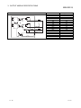
(6) Precautions for using the transistor output module
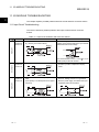
(a) Action against reverse current
If a transistor output module is wired as shown below, reverse current flows in
an output element, causing a failure of the element.
When wiring a transistor output module, connect a diode as shown below.
• When connecting transistor output modules in parallel
Sink type
Source type
• When incorporating an additional circuit parallel to a transistor output
module
Additional circuit
OUT
Additional circuit
OUT
Diode
COM
COM
Sink type
1-4
Diode
Source type
1-4
1
GENERAL SPECIFICATIONS AND PRECAUTIONS FOR USE
MELSEC-Q
(b) Measure against back EMF
When an inductive load is connected, connect a diode to the load in parallel.
Use a diode that meets the following conditions.
• Reverse breakdown voltage is 10 times as high as the circuit voltage or
more.
• Forward current is twice as high as the load current or more.
1-5
1-5
GENERAL SPECIFICATIONS AND PRECAUTIONS FOR USE
MELSEC-Q
(7) Precautions for using the contact output module
When using the contact output module, consider the following.
• Relay life (contact switching life)
• Effects to relay life due to connected load
• Measures against back EMF
(a) Relay life
Applicable module: QY10, QY10-TS, QY18A
The relay life depends on the operating environment.
Select a module according to the operating environment.
The relay lives shown below are the actual service values, not the guaranteed
values. Replace the module well in advance since the actual switching life may
be shorter than the one shown below.
200
100
70
Switching life (10,000 times)
1
50
30
20
10
7
30VDC =0ms
5
100VDC
=7ms
100VAC cos =0.7
200VAC cos =0.7
3
(L/R): Time constant
cos
: Power factor
100VAC cos =0.35
200VAC cos =0.35
24VDC =7ms
2
120VAC cos =0.2
240VAC cos =0.2
1
0.1
0.2
0.3
0.5
0.7
1
2
3
5
Switching current (A)
1-6
1-6
1
GENERAL SPECIFICATIONS AND PRECAUTIONS FOR USE
Operating environment
MELSEC-Q
Switching life
Rated switching voltage/current load
100 thousand times
200VAC 1.5A, 240VAC 1A (COS
100 thousand times
=0.7)
200VAC 0.4A, 240VAC 0.3A (COS
200VAC 1A, 240VAC 0.5A (COS
=0.7)
300 thousand times
=0.35)
100 thousand times
200VAC 0.3A, 240VAC 0.15A (COS
=0.35)
300 thousand times
24VDC 1A, 100VDC 0.1A (L/R=7ms)
100 thousand times
24VDC 0.3A, 100VDC 0.03A (L/R=7ms)
300 thousand times
POINT
When using the module for the application in which the relay contact is
frequently switched, the relay life span should be considered. It is recommended
to use a triac output module.
1-7
1-7
1
GENERAL SPECIFICATIONS AND PRECAUTIONS FOR USE
MELSEC-Q
(b) Measures against inrush current
The actual relay life may be significantly shortened compared to the one shown
in (7)(a), depending on the type of a load connected and the characteristics of
inrush current.
Also, the inrush current may cause contact welding.
Take the following measures to prevent shortening of the relay life and the
contact welding.
• Select a load so that the inrush current will be within the rated current of the
module.
• Connect an external relay that can withstand the inrush current.
The following table shows the relation between the load and the inrush current.
Select a load so that the inrush current (i) and the rated current (io) will be within
the rated switching current specified for the output module used.
The inrush current may flow for a longer time depending on the load.
Inrush
Load type
Signal waveform diagram
current(i)/rated
Inrush
Signal waveform diagram
current(i)/rated
current (io)
current (io)
Inductive
Approx. 10 to
Approx. 3 to
load
20 times
10 times
Approx. 3 to
Approx. 3
*1
times
10 times
Lamp load
Approx. 5 to
10 times
―
―
(To the next page)
*1: Typical electric-discharge lamp circuit includes discharge tubes,
transformers, choke coils, and capacitors. Therefore, note that the inrush
current may flow 20 to 40 times as large as the rated current in the case of
high power factor and low power impedance.
1-8
1-8
1
GENERAL SPECIFICATIONS AND PRECAUTIONS FOR USE
Inrush
Load type
Signal waveform diagram
current(i)/rated
Inrush
Signal waveform diagram
current (io)
Capacitive
Approx. 20 to
load
40 times
MELSEC-Q
current(i)/rated
current (io)
―
―
*2: When the wiring of the circuit is long, take care of the wire capacity.
1-9
1-9
1
GENERAL SPECIFICATIONS AND PRECAUTIONS FOR USE
MELSEC-Q
(c) Measures against back EMF
Configure a contact protection circuit for extending the contact life, preventing
noise when the contact is cut off, and suppressing the generation of carbide and
nitric acid due to arc discharge.
An Incorrect contact protection circuit may cause contact welding.
Also, when using the contact protection circuit, the recovery time may be long.
The following table shows the representative examples of the contact protection
circuit.
Circuit example
Method for selecting elements
Remarks
Capacitor +
Refer to the following for
If a load is from a relay or
Resistor method
constants of the capacitor and
solenoid, the recovery time
(CR method)
resistor. Note that the following
delays.
values may differ depending
A capacitor suppresses
on a nature of the load and a
electric discharge while a
variation of characteristics of it.
contact is off, and a resistor
• Capacitor 0.5 to 1 ( F)
restricts a flow of current while
against contact current of 1A
a contact is on.
• Resistor 0.5 to 1 (Ω)against
contact voltage of 1V
Use a capacitor whose
withstand voltage is 200 to
300V. In AC circuit, use a
capacitor having no polarity.
Diode method
Use a diode whose reverse
The recovery time is later than
breakdown voltage is 10 times
the CR method.
as high as the circuit voltage or
more and whose forward
current is twice as high as the
load current or more.
Diode + Zener
Use zener voltage for the
The diode method is effective
diode method
zener diode equal to or more
when the recovery time is too
than the power supply voltage.
late.
*1: When using AC power, impedance of CR must be larger enough than that of
the load. (prevention of a malfunction due to leak current from the CR)
(To the next page)
1 - 10
1 - 10
1
GENERAL SPECIFICATIONS AND PRECAUTIONS FOR USE
Circuit example
Varistor method
MELSEC-Q
Method for selecting elements
Remarks
Select a cut voltage (Vc) for
The recovery time delays
the varistor to meet the
slightly.
following condition. Multiply the
value by root two for use of AC
power.
Vc Power supply voltage
1.5 (V)
Note that when selecting an
element whose Vc is too high,
its effect will weaken.
POINT
(1) Avoid providing contact protection circuits shown below.
These circuits are effective for preventing an arc at shut-off. However, the
contact welding may occur because the charge current flows to capacitor when
the contact turns on or off.
A DC inductive load is usually harder for switching than a resistor load, but if a
proper protection circuit is configured, the performance will be similar to the
resistor load.
(2) A protection circuit must be provided closely to a load or contact (module). If
their distance is far, the protection circuit may not be effective. Appropriate
distance is within 50cm.
1 - 11
1 - 11
1
GENERAL SPECIFICATIONS AND PRECAUTIONS FOR USE
MELSEC-Q
(8) Precautions for using the triac output module
(a) Measures against back EMF
Circuit example
Method for selecting elements
Remarks
Capacitor +
Refer to the following for
If a load is from a relay or
Resistor method
constants of the capacitor and
solenoid, the recovery time
(CR method)
resistor. Note that the following
delays.
values may differ depending
on a nature of the load and a
variation of characteristics of it.
• Capacitor: 0.5 to 1 ( F)
against load current of 1A
• Resistor: 0.5 to 1(Ω) against
power supply voltage of 1V
Use a capacitor whose
withstand voltage is equal to or
more than the rated voltage.
Use a capacitor having no
polarity.
Varistor method
Select a cut voltage (Vc) for
The recovery time delays
the varistor to meet the
slightly.
following condition.
• Vc Power supply voltage
1.5 (V)
2 (when using AC
power supply)
Note that when selecting an
element whose Vc is too high,
its effect will weaken.
1 - 12
1 - 12
1
GENERAL SPECIFICATIONS AND PRECAUTIONS FOR USE
MELSEC-Q
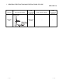
1.2.3 I/O combined module
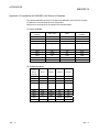
(1) I/O numbers of I/O combined modules
There are two types of I/O combined modules:
• Module using same I/O numbers for input and output
Since same number is used for input and output, the I/O numbers to be
used can be saved.
• Module using sequential I/O numbers for input and output
Since I/O assignments are the same for A series, it is useful when replacing
modules from those of A series.
00
Input (X)
Output (Y)
X00
Y00
Input (X)
00
X00
1F
X1F
32 points
1F
X1F
Output (Y)
Vacant
Y1F
20
32 points
Y20
32 points
Vacant
3F
Y3F
Module using same I/O numbers for input
Module using sequential I/O numbers for input
and output (QH42P)
and output (QX41Y41P)
Product
CPU module
Description
The module whose serial number
(first 5 digits) is "01112" or later
Precautions
• Use it with "Output" being set to
SW4D5C-GPPW or earlier
GX Developer
the I/O assignment.
• Input response time cannot be
set. (fixed at 10ms)
SW5D5C-GPPW or later
Use it with "I/O combined" being
set to the I/O assignment.
For how to check the serial number of the CPU module, refer to the QCPU User's
Manual (Hardware Design, Maintenance and Inspection).
1 - 13
1 - 13
1
GENERAL SPECIFICATIONS AND PRECAUTIONS FOR USE
MELSEC-Q
1.2.4 I/O module with protection function
The overload protection function and overheat protection function of the following
modules are explained below.
(1) QY40P, QY41P, QY42P, QX41Y41P, QH42P
Function
Common
(Overload and overheat
protection functions)
Overload protection
function
Overheat protection
function
Description
• If an overcurrent due to overload keeps flowing, heat is generated
and the overheat protection function is activated.
• The functions are provided for protecting only the circuits inside
the module.
A load error, which causes an increase in temperature within the
module, may deteriorate output elements or discolour the module
case or printed circuit board. If a load error occurs, turn off the
corresponding output immediately and eliminate the error cause.
• The overload protection function is activated in units of 1 point at
1A to 3A/point.
• The overload protection function returns to normal operation when
the load becomes a rated load.
• The overheat protection function is activated in units of 1 point.
• The overheat protection function automatically returns to normal
operation after heat reduces.
(2) QY81P, QY82P
Function
Common
(Overload and overheat
protection functions)
Overload protection
function
Overheat protection
function
1 - 14
Description
• If an overcurrent due to overload keeps flowing, heat is generated
and the overheat protection function is activated.
• The functions are provided for protecting only the circuits inside
the module.
A load error, which causes an increase in temperature within the
module, may deteriorate output elements or discolour the module
case or printed circuit board. If a load error occurs, turn off the
corresponding output immediately and eliminate the error cause.
• The overload protective function is activated in units of 1 point at
1A to 3A/point.
• The overload protective function returns to normal operation when
the load becomes a rated load.
• The overheat protection function is activated in units of 2 points.
(It is activated in units of 2 points of Y0/Y1, Y2/Y3, ..., and when
overheat protection is activated, 2 points of them are activated
simultaneously. If an overheat status persists, heat is conducted,
and which may activate another overheat protection function.)
• If an output turns on at the activation of the overheat protection
function, the actual output voltage oscillates between 0V and load
voltage.
At the load voltage of 24V, the average voltage during oscillation is
approx. 7V.
No oscillation occurs when the output is off at the activation of the
overheat protection function.
To ensure that the output is turned off at the activation of the
overheat protection function, use an external load that turns off at
7V or more.
• The overheat protective function automatically returns to normal
operation after heat reduces.
1 - 14
1
GENERAL SPECIFICATIONS AND PRECAUTIONS FOR USE
MELSEC-Q
1.2.5 Interrupt module
(1) If setting the response time during the interrupt input operation of QI60 or QX40H,
QX70H, QX80H, and QX90H, use the module whose contents are shown below.
The response time cannot be set with other contents (fixed at 0.2ms.).
Product
Description
CPU module
Product information "021120000000000-B" or later
GX Developer
SW6D5C-GPPW or later
For how to check product information of the CPU module, refer to the QCPU User's
Manual (Hardware Design, Maintenance and Inspection).
1.2.6 Installation and wiring
(1) Solderless terminal with insulation sleeve
A solderless terminal with insulation sleeve cannot be used for a terminal block.
It is recommended that the junction of a solderless terminal and a cable should be
covered up with a cable tag or an insulation tube.
(2) Applicable wire
2
Use wires of 0.3 to 0.75mm core and 2.8mm OD max. to connect to the terminal
block. When using a wire whose core is 0.75mm or more, it is preferable to use the
spring clamp terminal block (Q6TE-18S, Q6TE-18SN).
(3) Tightening torque range
Tighten screws (such as a module fixing screw) within the following torque range.
Screw location
1 - 15
Tightening torque range
Module fixing screw (M3 12 screw)
0.36 to 0.48 N•m
Terminal block screw (M3 screw)
0.42 to 0.58 N•m
Terminal block mounting screw (M3.5 screw)
0.66 to 0.89 N•m
Connector screw (M2.6 screw)
0.20 to 0.29 N•m
1 - 15
1
GENERAL SPECIFICATIONS AND PRECAUTIONS FOR USE
MELSEC-Q
1.3 Various Settings for I/O Module
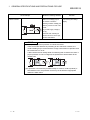
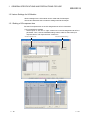
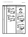
Various settings for the I/O module can be made with GX Developer.
This section describes how to make the settings with GX Developer.
1.3.1 Setting of I/O response time
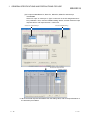
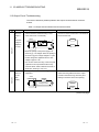
Set the I/O response time on the I/O assignment tab of PLC Parameter.
(1) For Input/I/O mix module
Select "Input" or "I/O mix" in "Type" combo box on the I/O assignment tab of PLC
parameter. Then, click the "Detailed setting" button, and then select the input
response time in "I/O response time" combo box.
Choose Input/I/O mix.
Choose Detailed setting.
Choose I/O response time
(default: 10ms).
1 - 16
1 - 16
1
GENERAL SPECIFICATIONS AND PRECAUTIONS FOR USE
MELSEC-Q
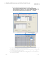
(2) For input module/QX40-S1, QX41-S1, QX42-S1, QX82-S1 and interrupt
module/QI60
Select "Hi. input" or "Interrupt" in "Type" combo box on the I/O assignment tab of
PLC parameter. Then, click the "Detailed setting" button, and then select the input
*1
response time in "I/O response time" combo box.
Choose Hi. input/Interrupt.
Choose Detailed setting.
Choose I/O response time
(default: 0.2ms).
*1: When the actual response time differs from the setting value, refer to the specifications of
the relevant input modules.
1 - 17
1 - 17
1
GENERAL SPECIFICATIONS AND PRECAUTIONS FOR USE
MELSEC-Q
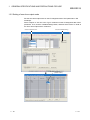
(3) For high-speed input module/QX40H, QX70H, QX80H, QX90H
Select "Hi.input" or "Interrupt", which is the same module type as the one selected
with the high-speed input module switch, in "Type" combo box on the I/O
*1
assignment tab of PLC parameter. Then, click the "Detailed setting" button, and
*2 *3
then select the input response time in "I/O response time"
combo box.
Choose Hi. input/Interrupt.
Choose Detailed setting.
Choose I/O response time
(default: 0.2ms).
*1: If a different module type from the one selected by the function selector switch (switch 2) of
the high-speed input module is selected, an error occurs.
*2: If the noise filter is disabled with the noise filter selector switch (switch 1) of the high-speed
input module, the setting value is ignored.
*3: When the actual response time differs from the setting value, refer to the specifications of
the relevant input modules.
1 - 18
1 - 18
1
GENERAL SPECIFICATIONS AND PRECAUTIONS FOR USE
MELSEC-Q
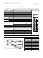
1.3.2 Setting of error-time output mode
Set the error-time output mode on the I/O assignment tab of PLC parameter in GX
Developer.
Select "Output" or "I/O mix" in the "Type" combo box on the I/O assignment tab of PLC
parameter. Then, click the "Detailed setting" button, and then select "Clear" or "Hold" in
the "Error time output mode" combo box.
Choose Output/I/O mix.
Choose Detailed setting.
Choose Clear/Hold
(default: Clear).
1 - 19
1 - 19
1
GENERAL SPECIFICATIONS AND PRECAUTIONS FOR USE
MELSEC-Q
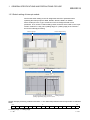
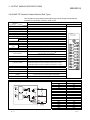
1.3.3 Switch setting of interrupt module
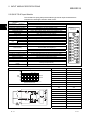
Perform the switch setting on the I/O assignment tab of PLC parameter when
operating the interrupt input for QI60, QX40H, QX70H, QX80H, or QX90H.
Select "Interrupt" in the "Type" combo box on the I/O assignment tab of PLC
parameter. Then, click the "Switch setting" button, and then select "HEX" in the "Input
format" combo box. Lastly, set 0 (leading edge) or 1 (trailing edge) in the "Switch 1"
box for the interrupt processing.
Choose Interrupt.
Choose Switch setting.
Choose HEX.
Set the interrupt processing conditions
Setting inhibited.
(leading edge/trailing edge) of CH1 to CH16.
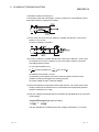
Set the interrupt processing condition with switch 1. The relationships between bits and inputs are as indicated
below.
b15
XF
to
XE
XD
XC
XB
XA
X9
X8
b0
X7
X6
X5
X4
X3
X2
X1
X0
0: Leading edge, 1: Trailing edge
1 - 20
1 - 20
2 INPUT MODULE SPECIFICATIONS
MELSEC-Q
2. INPUT MODULE SPECIFICATIONS
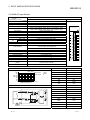
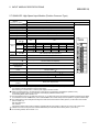
2.1 QX10 AC Input Module
Type
Specifications
Number of input points
Isolation method
Rated input voltage, frequency
Input voltage distortion
Rated input current
Input derating
Inrush current
ON voltage/ON current
OFF voltage/OFF current
Input impedance
OFF to ON
Response
time
ON to OFF
Dielectric withstand voltage
Insulation resistance
Noise immunity
Protection degree
Common terminal arrangement
Number of occupied I/O points
Operation indicator
External connections
Applicable wire size
Applicable crimping terminal
Internal current consumption
(5VDC)
Weight
AC input module
QX10
16 points
Photocoupler
100-120VAC (+10/-15%) 50/60Hz (±3Hz)
Within 5% (Refer to section 1.2)
Approx. 8mA (100VAC, 60Hz), approx. 7mA (100VAC, 50Hz)
Refer to the derating chart.
Max. 200mA within 1ms (at 132VAC)
80VAC or higher/5mA or higher (50Hz, 60Hz)
30VAC or lower/1.7mA or lower (50Hz, 60Hz)
Approx. 12kΩ (60Hz), approx. 15kΩ (50Hz)
15ms or less (100VAC 50Hz, 60Hz)
20ms or less (100VAC 50Hz, 60Hz)
1780VAC rms/3 cycles (altitude 2000m)
10MΩ or more by insulation resistance tester
By noise simulator of 1500Vp-p noise voltage, 1 s noise width
and 25 to 60Hz noise frequency
First transient noise IEC61000-4-4: 1kV
IP1X
16 points/common (common terminal: TB17)
16 points (I/O assignment is set as a 16-point input module.)
ON indication (LED)
18-point terminal block (M3 6 screws)
0.3 to 0.75mm2 core (2.8mm OD max.)
R1.25-3 (sleeved crimping terminals cannot be used.)
0
0
1
2
3
4
5
6
7
8
9
A
B
C
D
E
F
1
2
3
4
5
6
7
8
9
A
B
C
D
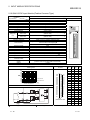
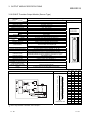
E
F
COM
NC
100VAC
8mA60Hz
7mA50Hz
0.17kg
120VAC
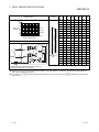
132VAC
10 20 30 40 50 55( C )
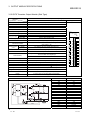
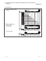
Ambient temperature
External connection
2-1
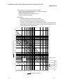
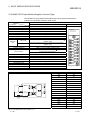
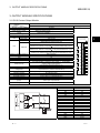
QX10
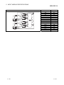
0 1 2 3 4 5 6 7
8 9 A B CDE F
50mA (TYP. all points ON)
Derating chart
(%)
100
90
ON 80
ratio 70
60
50
40
0
Appearance
Terminal block No.
Signal name
TB1
X00
TB2
X01
TB3
X02
TB4
X03
TB5
X04
TB6
X05
TB7
X06
TB8
X07
TB9
X08
TB10
X09
TB11
X0A
TB12
X0B
TB13
X0C
TB14
X0D
TB15
X0E
TB16
X0F
TB17
COM
TB18
Vacant
2-1
2
2 INPUT MODULE SPECIFICATIONS
MELSEC-Q
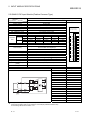
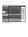
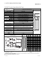
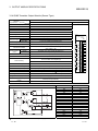
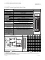
2.2 QX10-TS AC Input Module
This module is a spring clamp terminal block type and an input module that has
indicators for checking the insertion state of wire.
Type
Specifications
2
Number of input points
Isolation method
Rated input voltage, frequency
Input voltage distortion
Rated input current
Input derating
Inrush current
ON voltage/ON current
OFF voltage/OFF current
Input impedance
OFF to ON
Response
time
ON to OFF
Dielectric withstand voltage
Insulation resistance
Noise immunity
Protection degree
Common terminal arrangement
Number of occupied I/O points
Operation indicator
External connections
Applicable wire size
Applicable crimping terminal
Internal current consumption
(5VDC)
Weight
AC input module
QX10-TS
16 points
Photocoupler
100-120VAC (+10/-15%) 50/60Hz (±3Hz)
Within 5% (Refer to section 1.2)
Approx. 8mA (100VAC, 60Hz), approx. 7mA (100VAC, 50Hz)
Refer to the derating chart.
Max. 200mA within 1ms (at 132VAC)
80VAC or higher/5mA or higher (50Hz, 60Hz)
30VAC or lower/1.7mA or lower (50Hz, 60Hz)
Approx. 12kΩ (60Hz), approx. 15kΩ (50Hz)
15ms or less (100VAC 50Hz, 60Hz)
20ms or less (100VAC 50Hz, 60Hz)
1780VAC rms/3 cycles (altitude 2000m)
10MΩ or more by insulation resistance tester
By noise simulator of 1500Vp-p noise voltage, 1 s noise width
and 25 to 60Hz noise frequency
First transient noise IEC61000-4-4: 1kV
IP2X
16 points/common (common terminal: TB17)
16 points (I/O assignment is set as a 16-point input module.)
ON indication (LED)
Two piece Spring clamp terminal block
0.3 to 2.0mm2 core (22 to 15 AWG)
Refer to section 9.1
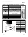
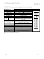
01234 567
8 9 ABCDEF
1
2
3
4
5
6
7
8
9
10
11
12
13
14
15
16
17
18
0.17kg
120VAC
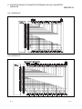
132VAC
10 20 30 40 50 55( C )
Ambient temperature
External connection
2-2
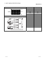
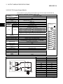
QX10-TS
50mA (TYP. all points ON)
Derating chart
(%)
100
90
ON 80
ratio 70
60
50
40
0
Appearance
Terminal block No.
Signal name
TB1
X00
TB2
X01
TB3
X02
TB4
X03
TB5
X04
TB6
X05
TB7
X06
TB8
X07
TB9
X08
TB10
X09
TB11
X0A
TB12
X0B
TB13
X0C
TB14
X0D
TB15
X0E
TB16
X0F
TB17
COM
TB18
Vacant
2-2
2 INPUT MODULE SPECIFICATIONS
MELSEC-Q
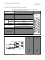
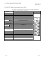
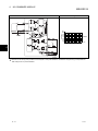
2.3 QX28 AC Input Module
Type
Specifications
Number of input points
Isolation method
Rated input voltage, frequency
Input voltage distortion
Rated input current
Input derating
Inrush current
ON voltage/ON current
OFF voltage/OFF current
Input impedance
OFF to ON
Response
time
ON to OFF
Dielectric withstand voltage
Insulation resistance
Noise immunity
Protection degree
Common terminal arrangement
Number of occupied I/O points
Operation indicator
External connections
Applicable wire size
Applicable crimping terminal
Internal current consumption
(5VDC)
Weight
AC input module
QX28
8 points
Photocoupler
100-240VAC (+10/-15%) 50/60Hz (±3Hz)
Within 5% (Refer to section 1.2)
Approx. 17mA (200VAC, 60Hz), approx. 14mA (200VAC, 50Hz)
Approx. 8mA (100VAC, 60Hz), approx. 7mA (100VAC, 50Hz)
Refer to the derating chart.
Max. 950mA within 1ms (at 264VAC)
80VAC or higher/5mA or higher (50Hz, 60Hz)
30VAC or lower/1.7mA or lower (50Hz, 60Hz)
Approx. 12kΩ (60Hz), approx. 15kΩ (50Hz)
10ms or less (100VAC 50Hz, 60Hz)
20ms or less (100VAC 50Hz, 60Hz)
2830VAC rms/3 cycles (altitude 2000m)
10MΩ or more by insulation resistance tester
By noise simulator of 1500Vp-p noise voltage, 1 s noise width
and 25 to 60Hz noise frequency
First transient noise IEC61000-4-4: 1kV
IP1X
8 points/common (common terminal: TB17)
16 points (I/O assignment is set as a 16-point input module.)
ON indication (LED)
18-point terminal block (M3 6 screws)
0.3 to 0.75mm2 core (2.8mm OD max.)
R1.25-3 (sleeved crimping terminals cannot be used.)
0
0
1
2
3
4
5
6
7
8
9
A
B
C
D
E
F
NC
1
NC
2
NC
3
NC
4
NC
5
NC
6
NC
7
NC
COM
NC
200VAC
17mA60Hz
14mA50Hz
0.20kg
100% 45 C
100% 55 C
87.5% 55 C
10 20 30 40 50 55( C )
Ambient temperature
External connection
2-3
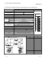
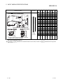
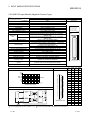
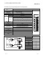
QX28
0 1 2 3 4 5 6 7
50mA (TYP. all points ON)
Derating chart
(%)
100
90
ON 80
ratio 70
60
50
40
0
Appearance
240V
264V
Terminal block No.
Signal name
TB1
X00
TB2
Vacant
TB3
X01
TB4
Vacant
TB5
X02
TB6
Vacant
TB7
X03
TB8
Vacant
TB9
X04
TB10
Vacant
TB11
X05
TB12
Vacant
TB13
X06
TB14
Vacant
TB15
X07
TB16
Vacant
TB17
COM
TB18
Vacant
2-3
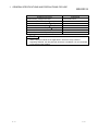
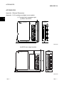
2 INPUT MODULE SPECIFICATIONS
MELSEC-Q
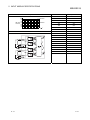
2.4 QX40 DC Input Module (Positive Common Type)
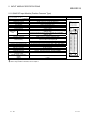
Type
DC input module (Positive common type)
Specifications
QX40
Number of input points
Isolation method
Rated input voltage
Rated input current
Input derating
ON voltage/ON current
OFF voltage/OFF current
Input impedance
Response
time
OFF to ON
ON to OFF
Dielectric withstand voltage
Insulation resistance
Noise immunity
Protection degree
Common terminal arrangement
Number of occupied I/O points
Operation indicator
External connections
Applicable wire size
Applicable crimping terminal
Internal current consumption
(5VDC)
Weight
Appearance
16 points
Photocoupler
24VDC (+20/-15%, ripple ratio within 5%)
Approx. 4mA
No
19V or higher/3mA or higher
11V or lower/1.7mA or lower
Approx. 5.6kΩ
1ms/5ms/10ms/20ms/70ms or less (configured in PLC parameter)
(Default: 10ms)
1ms/5ms/10ms/20ms/70ms or less (configured in PLC parameter)
(Default: 10ms)
560VAC rms/3 cycles (altitude 2000m)
10MΩ or more by insulation resistance tester
By noise simulator of 500Vp-p noise voltage, 1 s noise width
and 25 to 60Hz noise frequency
First transient noise IEC61000-4-4: 1kV
IP2X
16 points/common (common terminal: TB17)
16 points (I/O assignment is set as a 16-point input module.)
ON indication (LED)
18-point terminal block (M3 6 screws)
0.3 to 0.75mm2 core (2.8mm OD max.)
R1.25-3 (sleeved crimping terminals cannot be used.)
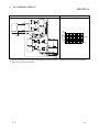
External connection
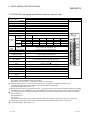
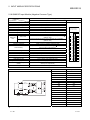
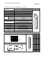
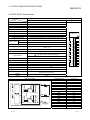
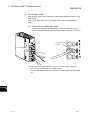
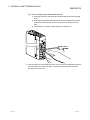
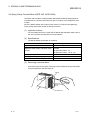
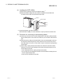
QX40
0 1 2 3 4 5 6 7
8 9 A B CDE F
1
0
0
1
2
3
4
5
6
7
8
9
A
B
C
D
E
F
1
2
1
3
4
5
6
7
8
9
A
B
C
D
E
F
- +
COM
NC
24VDC
4mA
50mA (TYP. all points ON)
0.16kg
Terminal block No.
Signal name
TB1
X00
TB2
X01
TB3
X02
TB4
X03
TB5
X04
TB6
X05
TB7
X06
TB8
X07
TB9
X08
TB10
X09
TB11
X0A
TB12
X0B
TB13
X0C
TB14
X0D
TB15
X0E
TB16
X0F
TB17
COM
TB18
Vacant
1: For the setting method, refer to Section 1.3.1.
2-4
2-4
2 INPUT MODULE SPECIFICATIONS
MELSEC-Q
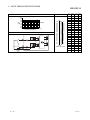
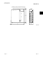
2.5 QX40-S1 DC Input Module (Positive Common Type)
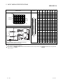
Type
Specifications
Number of input points
Isolation method
Rated input voltage
Rated input current
Input derating
ON voltage/ON current
OFF voltage/OFF current
Input impedance
Set value 1
TYP.
Response OFF to ON
MAX.
time
TYP.
ON to OFF
MAX.
Dielectric withstand voltage
Insulation resistance
Noise immunity
Protection degree
Common terminal arrangement
Number of occupied I/O points
Operation indicator
External connections
Applicable wire size
Applicable crimping terminal
Internal current consumption
(5VDC)
Weight
DC input module (Positive common type)
QX40-S1
16 points
Photocoupler
24VDC (+20/-15%, ripple ratio within 5%)
Approx. 6mA
No
19V or higher/4.0mA or higher
11V or lower/1.7mA or lower
Approx. 3.9kΩ
0.1
0.2
0.4
0.6
1
0.05ms
0.15ms
0.30ms
0.55ms
1.05ms
0.10ms
0.20ms
0.40ms
0.60ms
1.20ms
0.15ms
0.20ms
0.35ms
0.60ms
1.10ms
0.20ms
0.30ms
0.50ms
0.70ms
1.30ms
560VAC rms/3 cycles (altitude 2000m)
10MΩ or more by insulation resistance tester
By noise simulator of 500Vp-p noise voltage, 1 s noise width
and 25 to 60Hz noise frequency
First transient noise IEC61000-4-4: 1kV
IP2X
16 points/common (common terminal: TB17)
16 points (I/O assignment is set as a 16-point high-speed input module.)
ON indication (LED)
18-point terminal block (M3 6 screws)
0.3 to 0.75mm2 core (2.8mm OD max.)
R1.25-3 (sleeved crimping terminals cannot be used.)
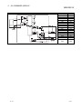
External connection
Appearance
QX40-S1
0 1 2 3 4 5 6 7
8 9 A B CDE F
0
0
1
2
3
4
5
6
7
8
9
A
B
C
D
E
F
1
2
3
4
5
6
7
8
9
A
B
C
D
E
F
- +
COM
NC
24VDC
6mA
60mA (TYP. all points ON)
0.20kg
Terminal block No.
Signal name
TB1
X00
TB2
X01
TB3
X02
TB4
X03
TB5
X04
TB6
X05
TB7
X06
TB8
X07
TB9
X08
TB10
X09
TB11
X0A
TB12
X0B
TB13
X0C
TB14
X0D
TB15
X0E
TB16
X0F
TB17
COM
TB18
Vacant
1: Configured in PLC parameter. (Default: 0.2ms)
A response time setting value can be changed in GX Developer (SW5D5C-GPPW or later).
For the setting method, refer to Section 1.3.1.
2-5
2-5
2 INPUT MODULE SPECIFICATIONS
MELSEC-Q
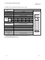
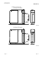
2.6 QX40-TS DC Input Module (Positive Common Type)
This module is a spring clamp terminal block type and an input module that has
indicators for checking the insertion state of wire.
Type
DC input module (Positive common type)
Specifications
QX40-TS
Number of input points
Isolation method
Rated input voltage
Rated input current
Input derating
ON voltage/ON current
OFF voltage/OFF current
Input impedance
Response
time
OFF to ON
ON to OFF
Dielectric withstand voltage
Insulation resistance
Noise immunity
Protection degree
Common terminal arrangement
Number of occupied I/O points
Operation indicator
External connections
Appearance
16 points
Photocoupler
24VDC (+20/-15%, ripple ratio within 5%)
Approx. 4mA
No
19V or higher/3mA or higher
11V or lower/1.7mA or lower
Approx. 5.6kΩ
1ms/5ms/10ms/20ms/70ms or less (configured in PLC parameter)
1
(Default: 10ms)
1ms/5ms/10ms/20ms/70ms or less (configured in PLC parameter)
1
(Default: 10ms)
560VAC rms/3 cycles (altitude 2000m)
10MΩ or more by insulation resistance tester
By noise simulator of 500Vp-p noise voltage, 1 s noise width
and 25 to 60Hz noise frequency
First transient noise IEC61000-4-4: 1kV
IP2X
16 points/common (common terminal: TB17)
16 points (I/O assignment is set as a 16-point input module.)
ON indication (LED)
Two piece Spring clamp terminal block
Applicable wire size
Applicable crimping terminal
Internal current consumption (5VDC)
Weight
External connection
0.3 to 2.0mm2 core (22 to 15 AWG)
Refer to section 9.1
50mA (TYP. all points ON)
0.16kg
QX40-TS
012 34 567
8 9 A B CDE F
1
2
3
4
5
6
7
8
9
10
11
12
13
14
15
16
17
18
Terminal block No.
Signal name
TB1
X00
TB2
X01
TB3
X02
TB4
X03
TB5
X04
TB6
X05
TB7
X06
TB8
X07
TB9
X08
TB10
X09
TB11
X0A
TB12
X0B
TB13
X0C
TB14
X0D
TB15
X0E
TB16
X0F
TB17
COM
TB18
Vacant
1: For the setting method, refer to Section 1.3.1.
2-6
2-6
2 INPUT MODULE SPECIFICATIONS
MELSEC-Q
2.7 QX40H DC High-Speed Input Module (Positive Common Type)
DC high-speed input module (Positive common type)
Type
Specifications
QX40H
Number of input points
Isolation method
Rated input voltage
Rated input current
Input derating
ON voltage/ON current
OFF voltage/OFF current
Input impedance
SW1 (noise
filter) 1
Set value 2
Response
TYP.
time
OFF to ON
MAX.
TYP.
ON to OFF
MAX.
Function
SW2 4
setting
Dielectric withstand voltage
Insulation resistance
Noise immunity
5
Appearance
16 points
Photocoupler
24VDC (+20/-15%, ripple ratio within 5%)
Approx. 6mA
Refer to the derating chart.
13V or higher/3mA or higher
8V or lower/1.6mA or lower
Approx. 3.9kΩ
OFF
ON
Invalid
0ms
0ms
-
3
3
3
3
0.1
0.04ms
0.05ms
0.04ms
0.05ms
0.2
0.10ms
0.15ms
0.10ms
0.15ms
0.4
0.25ms
0.30ms
0.25ms
0.30ms
0.6
0.50ms
0.60ms
0.50ms
0.60ms
1
0.95ms
1.00ms
0.95ms
1.00ms
OFF: Interrupt, ON: High-speed input
560VAC rms/3 cycles (altitude 2000m)
10MΩ or more by insulation resistance tester
By noise simulator of 500Vp-p noise voltage, 1 s noise width
and 25 to 60Hz noise frequency
IP2X
Protection degree
Common terminal
8 points/common (common terminal: TB9, TB18)
arrangement
Number of occupied I/O
16 points (I/O assignment is set as a 16-point high-speed input module or
points
interrupt module.) 4
Interrupt processing condition
Set by Switch setting in GX Developer 4 6
Operation indicator
ON indication (LED)
External connections
18-point terminal block (M3 6 screws)
Applicable wire size
0.3 to 0.75mm2 core (2.8mm OD max.)
Applicable crimping terminal
R1.25-3(sleeved solderless terminals cannot be used.)
Internal current consumption
80mA (TYP. all points ON)
(5VDC)
Weight
0.16kg
1: If the noise filter selector switch (switch 1) on the bottom of the module (refer to Chapter 10) is turned on, the noise filter takes effect.
The off-status noise filter disables I/O response time setting.
After switching on or off the switch 1, reset the power supply of the CPU module.
2: Set an input response time in "I/O response time" combo box of PLC parameter in GX Developer. (Default: 0.2ms)
A response time setting value can be changed in GX Developer (SW6D5C-GPPW or later).
For the setting details, refer to Section 1.3.1.
3: The actual response time is 5 s delay when turning on, 10 s delay when turning off, because the hardware response time is added.
For the details of the CPU overhead time, refer to manuals for the CPU module used (Function Explanation, Program Fundamentals).
4: The module function can be changed according to the status of the function selector switch (switch 2) on the bottom of the module
(refer to Chapter 10).
ON: High-speed input
OFF: Interrupt
If the function selector switch (switch 2) setting is changed while the CPU module is in RUN, an error (error code: 2100) occurs.
5: Indicates the noise immunity when the noise filter takes effect (the noise filter selector switch (switch 1) is turned on).
6: For the setting method, refer to Section 1.3.3.
2-7
2-7
2 INPUT MODULE SPECIFICATIONS
MELSEC-Q
Derating chart
(%)
100
90
80
ON ratio/ 70
common
60
50
40
0
26.4VDC
28.8VDC
10 20 30 40 50 55 (
Ambient temperature
External connection
2-8
)
Terminal block No.
Signal name
TB1
X00
TB2
X01
TB3
X02
TB4
X03
TB5
X04
TB6
X05
TB7
X06
TB8
X07
TB9
COM1
TB10
X08
TB11
X09
TB12
X0A
TB13
X0B
TB14
X0C
TB15
X0D
TB16
X0E
TB17
X0F
TB18
COM2
2-8
2 INPUT MODULE SPECIFICATIONS
MELSEC-Q
2.8 QX41 DC Input Module (Positive Common Type)
Type
Specifications
QX41
32 points
Photocoupler
24VDC (+20/-15%, ripple ratio within 5%)
Approx. 4mA
Refer to the derating chart.
19V or higher/3mA or higher
11V or lower/1.7mA or lower
Approx. 5.6kΩ
1ms/5ms/10ms/20ms/70ms or less (configured in PLC parameter)
(Default: 10ms)
1ms/5ms/10ms/20ms/70ms or less (configured in PLC parameter)
Number of input points
Isolation method
Rated input voltage
Rated input current
Input derating
ON voltage/ON current
OFF voltage/OFF current
Input impedance
Response
time
DC input module (Positive common type)
OFF to ON
ON to OFF
Dielectric withstand voltage
Insulation resistance
Noise immunity
Protection degree
Common terminal arrangement
Number of occupied I/O points
Operation indicator
External connections
Applicable wire size
Applicable connector
Applicable connector/terminal block
converter module
Internal current consumption
(5VDC)
Weight
QX41
0 1
8 9
0 1
8 9
1
2
A
2
A
3
B
3
B
4
C
4
C
24VDC
4mA
5
D
5
D
6
E
6
E
7
F
7
F
QX41
1
(Default: 10ms)
560VAC rms/3 cycles (altitude 2000m)
10MΩ or more by insulation resistance tester
By noise simulator of 500Vp-p noise voltage, 1 s noise width
and 25 to 60Hz noise frequency
First transient noise IEC61000-4-4: 1kV
IP2X
32 points/common (common terminal: B01, B02)
32 points (I/O assignment is set as a 32-point input module.)
ON indication (LED)
40-pin connector
0.088 to 0.3mm2 (For A6CON1 or A6CON4) 2
A6CON1, A6CON2, A6CON3, A6CON4 (optional)
A6TBXY36, A6TBXY54, A6TBX70
75mA (TYP. all points ON)
(0.08A is shown on the rating plate of the module.)
0.15kg
Derating chart
(%)
100
90
80
ON
ratio 70
60
50
40
0
Appearance
Pin-Outs
28.8VDC
10 20 30 40 50 55 ( C )
Ambient temperature
External connection
B20
B19
B18
B17
B16
B15
B14
B13
B12
B11
B10
B9
B8
B7
B6
B5
B4
B3
B2
B1
A20
A19
A18
A17
A16
A15
A14
A13
A12
A11
A10
A9
A8
A7
A6
A5
A4
A3
A2
A1
Pin
No.
Signal
No.
Pin
No.
Signal
No.
B20
X00
A20
X10
B19
X01
A19
X11
B18
X02
A18
X12
B17
X03
A17
X13
B16
X04
A16
X14
B15
X05
A15
X15
B14
X06
A14
X16
B13
X07
A13
X17
B12
X08
A12
X18
B11
X09
A11
X19
B10
X0A
A10
X1A
B09
X0B
A09
X1B
B08
X0C
A08
X1C
B07
X0D
A07
X1D
B06
X0E
A06
X1E
B05
X0F
A05
X1F
B04 Vacant A04 Vacant
Module front view
1: For the setting method, refer to Section 1.3.1.
2-9
B03 Vacant A03 Vacant
B02
COM
A02 Vacant
B01
COM
A01 Vacant
2: When using A6CON2 or A6CON3, refer to Chapter 7.
2-9
2 INPUT MODULE SPECIFICATIONS
MELSEC-Q
2.9 QX41-S1 DC Input Module (Positive Common Type)
Type
Specifications
Number of input points
Isolation method
Rated input voltage
Rated input current
Input derating
ON voltage/ON current
OFF voltage/OFF current
Input impedance
Set value 1
TYP.
Response OFF to ON
MAX.
time
TYP.
ON to OFF
MAX.
Dielectric withstand voltage
Insulation resistance
Noise immunity
Protection degree
Common terminal arrangement
Number of occupied I/O points
Operation indicator
External connections
Applicable wire size
Applicable connector
Applicable connector/terminal
block converter module
Internal current consumption
(5VDC)
Weight
DC input module (Positive common type)
QX41-S1
32 points
Photocoupler
24VDC (+20/-15%, ripple ratio within 5%)
Approx. 4mA
Refer to the derating chart.
19V or higher/3.0mA or higher
9.5V or lower/1.5mA or lower
Approx. 5.6kΩ
0.1
0.2
0.4
0.6
1
0.05ms
0.15ms
0.30ms
0.55ms
1.05ms
0.12ms
0.20ms
0.40ms
0.60ms
1.20ms
0.15ms
0.20ms
0.35ms
0.60ms
1.10ms
0.20ms
0.30ms
0.50ms
0.70ms
1.30ms
560VAC rms/3 cycles (altitude 2000m)
10MΩ or more by insulation resistance tester
By noise simulator of 500Vp-p noise voltage, 1 s noise width
and 25 to 60Hz noise frequency
First transient noise IEC61000-4-4: 1kV
IP2X
32 points/common (common terminal: B01, B02)
32 points (I/O assignment is set as a 32-point high-speed input module.)
ON indication (LED)
40-pin connector
0.088 to 0.3mm2 (For A6CON1 or A6CON4) 2
Appearance
QX41-S1
0 1 2 3
8 9 A B
0 1 2 3
8 9 A B
24VDC
4mA
4
C
4
C
5
D
5
D
6
E
6
E
7
F
7
F
QX41-S1
A6CON1, A6CON2, A6CON3, A6CON4 (optional)
A6TBXY36, A6TBXY54, A6TBX70
75mA (TYP. all points ON)
(0.08A is shown on the rating plate of the module.)
0.15kg
1: Configured in PLC parameter. (Default: 0.2ms)
A response time setting value can be changed in GX Developer (SW5D5C-GPPW or later).
For the setting method, refer to Section 1.3.1.
2: When using A6CON2 or A6CON3, refer to Chapter 7.
2 - 10
2 - 10
2 INPUT MODULE SPECIFICATIONS
MELSEC-Q
Derating chart
(%)
100
90
80
ON
ratio 70
60
50
40
0
Pin-Outs
28.8VDC
10 20 30 40 50 55 ( C )
Ambient temperature
External connection
B20
B19
B18
B17
B16
B15
B14
B13
B12
B11
B10
B9
B8
B7
B6
B5
B4
B3
B2
B1
A20
A19
A18
A17
A16
A15
A14
A13
A12
A11
A10
A9
A8
A7
A6
A5
A4
A3
A2
A1
Pin
No.
Signal
No.
Pin
No.
Signal
No.
B20
X00
A20
X10
B19
X01
A19
X11
B18
X02
A18
X12
B17
X03
A17
X13
B16
X04
A16
X14
B15
X05
A15
X15
B14
X06
A14
X16
B13
X07
A13
X17
B12
X08
A12
X18
B11
X09
A11
X19
B10
X0A
A10
X1A
B09
X0B
A09
X1B
B08
X0C
A08
X1C
B07
X0D
A07
X1D
B06
X0E
A06
X1E
B05
X0F
A05
X1F
B04 Vacant A04 Vacant
Module front view
2 - 11
B03 Vacant A03 Vacant
B02
COM
A02 Vacant
B01
COM
A01 Vacant
2 - 11
2 INPUT MODULE SPECIFICATIONS
MELSEC-Q
2.10 QX41-S2 DC Input Module (Positive Common Type)
Type
Specifications
QX41-S2
32 points
Photocoupler
24VDC (+20/-15%, ripple ratio within 5%)
Approx. 6mA
Refer to the derating chart.
15V or higher/3mA or higher
5V or lower/1.7mA or lower
Approx. 3.6kΩ
1ms/5ms/10ms/20ms/70ms or less (configured in PLC parameter) 1
(Default: 10ms)
1ms/5ms/10ms/20ms/70ms or less (configured in PLC parameter) 1
(Default: 10ms)
560VAC rms/3 cycles (altitude 2000m)
10MΩ or more by insulation resistance tester
By noise simulator of 500Vp-p noise voltage, 1 s noise width
and 25 to 60Hz noise frequency
First transient noise IEC61000-4-4: 1kV
IP2X
32 points/common (common terminal: B01, B02)
32 points (I/O assignment is set as a 32-point input module.)
ON indication (LED)
40-pin connector
0.088 to 0.3mm2 (For A6CON1 or A6CON4) 2
Number of input points
Isolation method
Rated input voltage
Rated input current
Input derating
ON voltage/ON current
OFF voltage/OFF current
Input impedance
Response
time
DC input module (Positive common type)
OFF to ON
ON to OFF
Dielectric withstand voltage
Insulation resistance
Noise immunity
Protection degree
Common terminal arrangement
Number of occupied I/O points
Operation indicator
External connections
Applicable wire size
Applicable connector
Applicable connector/terminal block
converter module
Internal current consumption
(5VDC)
Weight
A6CON1, A6CON2, A6CON3, A6CON4 (optional)
A6TBXY36, A6TBXY54, A6TBX70
75mA (TYP. all points ON)
(0.08A is shown on the rating plate of the module.)
0.15kg
Derating chart
(%)
100
90
80
70
ON
ratio 60
50
40
30
20
10
0
Pin-Outs
(31.25%) 24VDC
(18.75%) 28.8VDC
10 20 30 40
Ambient temperature
Appearance
50 55 (
External connection
)
B20
B19
B18
B17
B16
B15
B14
B13
B12
B11
B10
B9
B8
B7
B6
B5
B4
B3
B2
B1
A20
A19
A18
A17
A16
A15
A14
A13
A12
A11
A10
A9
A8
A7
A6
A5
A4
A3
A2
A1
Pin
No.
Signal
No.
Pin
No.
Signal
No.
B20
X00
A20
X10
B19
X01
A19
X11
B18
X02
A18
X12
B17
X03
A17
X13
B16
X04
A16
X14
B15
X05
A15
X15
B14
X06
A14
X16
B13
X07
A13
X17
B12
X08
A12
X18
B11
X09
A11
X19
B10
X0A
A10
X1A
B09
X0B
A09
X1B
B08
X0C
A08
X1C
B07
X0D
A07
X1D
B06
X0E
A06
X1E
B05
X0F
A05
X1F
B04 Vacant A04 Vacant
Module front view
1: For the setting method, refer to Section 1.3.1.
2 - 12
B03 Vacant A03 Vacant
B02
COM
A02 Vacant
B01
COM
A01 Vacant
2: When using A6CON2 or A6CON3, refer to Chapter 7.
2 - 12
2 INPUT MODULE SPECIFICATIONS
MELSEC-Q
2.11 QX42 DC Input Module (Positive Common Type)
Type
Specifications
Number of input points
Isolation method
Rated input voltage
Rated input current
Input derating
ON voltage/ON current
OFF voltage/OFF current
Input impedance
Response
time
OFF to ON
ON to OFF
Dielectric withstand voltage
Insulation resistance
Noise immunity
Protection degree
Common terminal arrangement
Number of occupied I/O points
Operation indicator
External connections
Applicable wire size
Applicable connector
Applicable connector/terminal block
converter module
Internal current consumption
(5VDC)
Weight
DC input module (Positive common type)
QX42
64 points
Photocoupler
24VDC (+20/-15%, ripple ratio within 5%)
Approx. 4mA
Refer to the derating chart.
19V or higher/3mA or higher
11V or lower/1.7mA or lower
Approx. 5.6kΩ
1ms/5ms/10ms/20ms/70ms or less (configured in PLC parameter) 1
(Default: 10ms)
1ms/5ms/10ms/20ms/70ms or less (configured in PLC parameter) 1
(Default: 10ms)
560VAC rms/3 cycles (altitude 2000m)
10MΩ or more by insulation resistance tester
By noise simulator of 500Vp-p noise voltage, 1 s noise width
and 25 to 60Hz noise frequency
First transient noise IEC61000-4-4: 1kV
IP2X
32 points/common (common terminal: 1B01, 1B02, 2B01, 2B02)
64 points (I/O assignment is set as a 64-point input module.)
ON indication (LED), 32 point switch-over using switch
40-pin connector
0.088 to 0.3mm2 (For A6CON1 or A6CON4) 2
A6CON1, A6CON2, A6CON3, A6CON4 (optional)
Appearance
QX42
0 1
8 9
0 1
8 9
2
A
2
A
24VDC
4mA
3
B
3
B
4
C
4
C
5
D
5
D
6
E
6
E
7
F
7
F
F
QX42
DISPLAY
L
A6TBXY36, A6TBXY54, A6TBX70
90mA (TYP. all points ON)
0.18kg
1: For the setting method, refer to Section 1.3.1.
2: When using A6CON2 or A6CON3, refer to Chapter 7.
2 - 13
2 - 13
2 INPUT MODULE SPECIFICATIONS
MELSEC-Q
Derating chart
(%)
100
90
80
70
ON ratio/
common 60
50
40
30
20
0
Pin-Outs
24VDC
26.4VDC
28.8VDC
10 20 30 40 50 55 ( C )
Ambient temperature
External connection
B20
B19
B18
B17
B16
B15
B14
B13
B12
B11
B10
B9
B8
B7
B6
B5
B4
B3
B2
B1
A20
A19
A18
A17
A16
A15
A14
A13
A12
A11
A10
A9
A8
A7
A6
A5
A4
A3
A2
A1
Module front
view
Pin
No.
4
Signal
No.
Pin
No.
4
Signal
No.
Pin
No.
4
Signal
No.
Pin
No.
4
Signal
No.
1B20
X00
1A20
X10
2B20
X20
2A20
X30
1B19
X01
1A19
X11
2B19
X21
2A19
X31
1B18
X02
1A18
X12
2B18
X22
2A18
X32
1B17
X03
1A17
X13
2B17
X23
2A17
X33
1B16
X04
1A16
X14
2B16
X24
2A16
X34
1B15
X05
1A15
X15
2B15
X25
2A15
X35
1B14
X06
1A14
X16
2B14
X26
2A14
X36
1B13
X07
1A13
X17
2B13
X27
2A13
X37
1B12
X08
1A12
X18
2B12
X28
2A12
X38
1B11
X09
1A11
X19
2B11
X29
2A11
X39
1B10
X0A
1A10
X1A
2B10
X2A
2A10
X3A
1B09
X0B
1A09
X1B
2B09
X2B
2A09
X3B
1B08
X0C
1A08
X1C
2B08
X2C
2A08
X3C
1B07
X0D
1A07
X1D
2B07
X2D
2A07
X3D
1B06
X0E
1A06
X1E
2B06
X2E
2A06
X3E
1B05
X0F
1A05
X1F
2B05
X2F
2A05
X3F
1B04 Vacant 1A04 Vacant 2B04 Vacant 2A04 Vacant
1B03 Vacant 1A03 Vacant 2B03 Vacant 2A03 Vacant
1B02 COM1 1A02 Vacant 2B02
COM2
2A02 Vacant
1B01 COM1 1A01 Vacant 2B01
COM2
2A01 Vacant
The above diagram shows the first half of 32 points (F).
The latter half of 32 points (L) are similar.
3: Selection of left-hand (F) side provides the first half (X00 to X1F) LED indications, and selection of right-hand (L) side provides the
latter half (X20 to X3F) LED indications.
4: Pin number of 1
indicates that of the left-hand side connector, and pin number of 2
indicates that of the right-hand
side connector.
2 - 14
2 - 14
2 INPUT MODULE SPECIFICATIONS
MELSEC-Q
2.12 QX42-S1 DC Input Module (Positive Common Type)
Type
Specifications
Number of input points
Isolation method
Rated input voltage
Rated input current
Input derating
ON voltage/ON current
OFF voltage/OFF current
Input impedance
Set value 1
TYP.
Response OFF to ON
MAX.
time
TYP.
ON to OFF
MAX.
Dielectric withstand voltage
Insulation resistance
Noise immunity
Protection degree
Common terminal arrangement
Number of occupied I/O points
Operation indicator
External connections
Applicable wire size
Applicable connector
Applicable connector/terminal
block converter module
Internal current consumption
(5VDC)
Weight
DC input module (Positive common type)
QX42-S1
64 points
Photocoupler
24VDC (+20/-15%, ripple ratio within 5%)
Approx. 4mA
Refer to the derating chart.
19V or higher/3.0mA or higher
9.5V or lower/1.5mA or lower
Approx. 5.6kΩ
0.1
0.2
0.4
0.6
1
0.05ms
0.15ms
0.30ms
0.55ms
1.05ms
0.12ms
0.20ms
0.40ms
0.60ms
1.20ms
0.15ms
0.20ms
0.35ms
0.60ms
1.10ms
0.20ms
0.30ms
0.50ms
0.70ms
1.30ms
560VAC rms/3 cycles (altitude 2000m)
10MΩ or more by insulation resistance tester
By noise simulator of 500Vp-p noise voltage, 1 s noise width
and 25 to 60Hz noise frequency
First transient noise IEC61000-4-4: 1kV
IP2X
32 points/common (common terminal: 1B01, 1B02, 2B01, 2B02)
64 points (I/O assignment is set as a 64-point high-speed input module.)
ON indication (LED), 32 point switch-over using switch
40-pin connector
0.088 to 0.3mm2 (For A6CON1 or A6CON4) 2
A6CON1, A6CON2, A6CON3, A6CON4 (optional)
Appearance
QX42-S1
0 1 2 3
8 9 A B
0 1 2 3
8 9 A B
4
C
4
C
5
D
5
D
24VDC
4mA
F
QX42-S1
DISPLAY
L
6
E
6
E
7
F
7
F
A6TBXY36, A6TBXY54, A6TBX70
90mA (TYP. all points ON)
0.18kg
1: Configured in PLC parameter. (Default: 0.2ms)
A response time setting value can be changed in GX Developer (SW5D5C-GPPW or later).
For the setting method, refer to Section 1.3.1.
2: When using A6CON2 or A6CON3, refer to Chapter 7.
2 - 15
2 - 15
2 INPUT MODULE SPECIFICATIONS
Derating chart
(%)
100
90
80
ON ratio/ 70
common 60
50
40
30
20
0
MELSEC-Q
Pin-Outs
24VDC
26.4VDC
28.8VDC
10 20 30 40 50 55 ( C )
Ambient temperature
External connection
B20
B19
B18
B17
B16
B15
B14
B13
B12
B11
B10
B9
B8
B7
B6
B5
B4
B3
B2
B1
A20
A19
A18
A17
A16
A15
A14
A13
A12
A11
A10
A9
A8
A7
A6
A5
A4
A3
A2
A1
Module front
view
Pin
No.
4
Signal
No.
Pin
No.
4
Signal
No.
Pin
No.
4
Signal
No.
Pin
No.
4
Signal
No.
1B20
X00
1A20
X10
2B20
X20
2A20
X30
1B19
X01
1A19
X11
2B19
X21
2A19
X31
1B18
X02
1A18
X12
2B18
X22
2A18
X32
1B17
X03
1A17
X13
2B17
X23
2A17
X33
1B16
X04
1A16
X14
2B16
X24
2A16
X34
1B15
X05
1A15
X15
2B15
X25
2A15
X35
1B14
X06
1A14
X16
2B14
X26
2A14
X36
1B13
X07
1A13
X17
2B13
X27
2A13
X37
1B12
X08
1A12
X18
2B12
X28
2A12
X38
1B11
X09
1A11
X19
2B11
X29
2A11
X39
1B10
X0A
1A10
X1A
2B10
X2A
2A10
X3A
1B09
X0B
1A09
X1B
2B09
X2B
2A09
X3B
1B08
X0C
1A08
X1C
2B08
X2C
2A08
X3C
1B07
X0D
1A07
X1D
2B07
X2D
2A07
X3D
1B06
X0E
1A06
X1E
2B06
X2E
2A06
X3E
1B05
X0F
1A05
X1F
2B05
X2F
2A05
X3F
1B04 Vacant 1A04 Vacant 2B04 Vacant 2A04 Vacant
1B03 Vacant 1A03 Vacant 2B03 Vacant 2A03 Vacant
1B02 COM1 1A02 Vacant 2B02 COM2 2A02 Vacant
1B01 COM1 1A01 Vacant 2B01 COM2 2A01 Vacant
The above diagram shows the first half of 32 points (F).
The latter half of 32 points (L) are similar.
3: Selection of left-hand (F) side provides the first half (X00 to X1F) LED indications, and selection of right-hand (L) side provides the
latter half (X20 to X3F) LED indications.
indicates that of the left-hand side connector, and pin number of 2
indicates that of the right-hand
4: Pin number of 1
side connector.
2 - 16
2 - 16
2 INPUT MODULE SPECIFICATIONS
MELSEC-Q
2.13 QX50 DC (Positive Common/Negative Common Shared Type)/ AC Input Module
DC (positive/negative shared common type)/ AC input module
QX50
Appearance
DC Input
AC Input
16 points
Photocoupler
QX50
012 345 67
48VDC
48VAC (+10/-15%) 50/60Hz
8 9 A BCDEF
(+20/-15%, ripple ratio within 5%)
(±3Hz) (ripple ratio within 5%)
Approx. 4mA
Refer to the derating chart.
28V or higher/2.5mA or higher
0
10V or lower/1.0mA or lower
0
1
Approx. 11.2kΩ
2
1
5ms or less
15ms or less
3
2
20ms or less
20ms or less
4
3
1060VAC rms/3 cycles (altitude 2000m)
5
4
6
10MΩ or more by insulation resistance tester
5
7
By noise simulator of 500Vp-p noise voltage, 1 s noise width
6
8
and 25 to 60Hz noise frequency
9
7
First transient noise IEC61000-4-4: 1kV
A
8
IP2X
B
9
16 points/common (common terminal: TB17)
C
A
16 points (I/O assignment is set as a 16-point input module.)
D
B
ON indication (LED)
E
F
C
18-point terminal block (M3 6 screws)
0.3 to 0.75mm2 core (2.8mm OD max.)
D
R1.25-3 (sleeved crimping terminals cannot be used.)
E
Type
Specifications
Number of input points
Isolation method
Rated input voltage
Rated input current
Input derating
ON voltage/ON current
OFF voltage/OFF current
Input impedance
OFF to ON
Response
time 1
ON to OFF
Dielectric withstand voltage
Insulation resistance
Noise immunity
Protection degree
Common terminal arrangement
Number of occupied I/O points
Operation indicator
External connections
Applicable wire size
Applicable crimping terminal
Internal current consumption
(5VDC)
Weight
F
50mA (TYP. all points ON)
0.13kg
Derating chart
Terminal block No.
Signal name
TB1
X00
TB2
X01
TB3
X02
TB4
X03
TB5
X04
TB6
X05
TB7
X06
TB8
X07
TB9
X08
TB10
X09
TB11
X0A
(%)
100
90
80
ON 70
ratio
60
50
40
0
48VDC/AC
57.6VDC
52.8VAC
10
20
30
40
50 55 ( C)
Ambient temperature
External connection
TB12
X0B
TB13
X0C
TB14
X0D
TB15
X0E
TB16
X0F
TB17
COM
TB18
Vacant
1: Response time cannot be changed. Parameter setting of the CPU module will be invalid.
2 - 17
2 - 17
2 INPUT MODULE SPECIFICATIONS
MELSEC-Q
2.14 QX70 DC Input Module (Positive Common/Negative Common Shared Type)
Type
DC input module (Positive/negative shared common type)
QX70
Specifications
Number of input points
Isolation method
5VDC
(+20/-10%, ripple ratio within 5%)
Approx. 1.2mA
Applicable wire size
12VDC
(+20/-15%, ripple ratio within 5%)
Approx. 3.3mA
None
3.5V or higher/1mA or higher
1V or lower/0.1mA or lower
Approx. 3.3kΩ
1ms/5ms/10ms/20ms/70ms or less (configured in PLC parameter) 1
(Default: 10ms)
1ms/5ms/10ms/20ms/70ms or less (configured in PLC parameter) 1
(Default: 10ms)
560VAC rms/3 cycles (altitude 2000m)
10MΩ or more by insulation resistance tester
By noise simulator of 500Vp-p noise voltage,
1 s noise width and 25 to 60Hz noise frequency
First transient noise IEC61000-4-4: 0.25kV
IP2X
16 points/common (common terminal: TB17)
16 points (I/O assignment is set as a 16-point input module.)
ON indication (LED)
18-point terminal block (M3 6 screw)
Core cable: 0.3 to 0.75mm2 (Outside diameter: 2.8mm or smaller)
Applicable crimping terminal
Internal current consumption
(5VDC)
Weight
R1.25-3 (Terminals with sleeve cannot be used)
55mA (TYP, all points ON)
(0.06A is shown on the rating plate of the module.)
0.14kg
Rated input voltage
Rated input current
Input derating
ON voltage/ON current
OFF voltage/OFF current
Input resistance
Response
time
Appearance
16 points
Photocoupler
OFF to ON
ON to OFF
Dielectric withstand voltage
Insulation resistance
Noise immunity
Protection degree
Common terminal arrangement
Number of occupied I/O points
Operation indicator
External connections
External connection
QX70
0 1 2 3 4 5 6 7
8 9 A B CDE F
0
0
1
2
3
4
5
6
7
8
9
A
B
C
D
E
F
1
2
3
4
5
6
7
8
9
A
B
C
D
E
F
- +
COM
NC
5/12VDC
1.2mA
3.3mA
Terminal block No.
Signal name
TB1
X00
TB2
X01
TB3
X02
TB4
X03
TB5
X04
TB6
X05
TB7
X06
TB8
X07
TB9
X08
TB10
X09
TB11
X0A
TB12
X0B
TB13
X0C
TB14
X0D
TB15
X0E
TB16
X0F
TB17
COM
TB18
Vacant
1: For the setting method, refer to Section 1.3.1.
2 - 18
2 - 18
2 INPUT MODULE SPECIFICATIONS
MELSEC-Q
2.15 QX70H DC High-speed Input Module (Positive Common Type)
DC high-speed input module (Positive common type)
Type
Specifications
QX70H
Number of input points
Isolation method
Rated input voltage
Rated input current
Input derating
ON voltage/ON current
OFF voltage/OFF current
Input impedance
SW1 (noise
filter) 1
Set value 2
Response
TYP.
time
OFF to ON
MAX.
TYP.
ON to OFF
MAX.
Function
SW2 4
setting
Dielectric withstand voltage
Insulation resistance
Noise immunity
5
Protection degree
Common terminal
arrangement
Number of occupied I/O
points
Interrupt processing condition
Operation indicator
External connections
Applicable wire size
Applicable crimping terminal
Internal current consumption
(5VDC)
Weight
Appearance
16 points
Photocoupler
5VDC (+20/-15%, ripple ratio within 5%)
Approx. 6mA
None
3.5V or higher/3mA or higher
1V or lower/1mA or lower
Approx. 470Ω
OFF
ON
Invalid
0ms
0ms
-
3
3
3
3
0.1
0.04ms
0.05ms
0.04ms
0.05ms
0.2
0.10ms
0.15ms
0.10ms
0.15ms
0.4
0.25ms
0.30ms
0.25ms
0.30ms
0.6
0.50ms
0.60ms
0.50ms
0.60ms
1
0.95ms
1.00ms
0.95ms
1.00ms
OFF: Interrupt, ON: High-speed input
560VAC rms/3 cycles (altitude 2000m)
10MΩ or more by insulation resistance tester
By noise simulator of 500Vp-p noise voltage, 1 s noise width
and 25 to 60Hz noise frequency
IP2X
8 points/common (common terminal: TB9, TB18)
16 points (I/O assignment is set as a 16-point high-speed input module or
interrupt module.) 4
Set by Switch setting in GX Developer 4 6
ON indication (LED)
18-point terminal block (M3 6 screws)
0.3 to 0.75mm2 core (2.8mm OD max.)
R1.25-3 (sleeved solderless terminals cannot be used.)
80mA (TYP. all points ON)
0.14kg
1: If the noise filter selector switch (switch 1) on the bottom of the module (refer to Chapter 10) is turned on, the noise filter takes effect.
The off-status noise filter disables I/O response time setting.
After switching on or off the switch 1, reset the power supply of the CPU module.
2: Set an input response time in "I/O response time" combo box of PLC parameter in GX Developer. (Default: 0.2ms)
A response time setting value can be changed in GX Developer (SW6D5C-GPPW or later).
For the setting details, refer to Section 1.3.1.
3: The actual response time is 5 s delay when turning on, 10 s delay when turning off, because the hardware response time is added.
For the details of the CPU overhead time, refer to manuals for the CPU module used (Function Explanation, Program Fundamentals).
4: The module function can be changed according to the status of the function selector switch (switch 2) on the bottom of the module
(refer to Chapter 10).
ON: High-speed input
OFF: Interrupt
If the function selector switch (switch 2) setting is changed while the CPU module is in RUN, an error (error code: 2100) occurs.
5: Indicates the noise immunity when the noise filter takes effect (the noise filter selector switch (switch 1) is turned on).
6: For the setting method, refer to Section 1.3.3.
2 - 19
2 - 19
2 INPUT MODULE SPECIFICATIONS
External connection
2 - 20
MELSEC-Q
Terminal block No.
Signal name
TB1
TB2
TB3
TB4
TB5
TB6
TB7
TB8
TB9
TB10
TB11
TB12
TB13
TB14
TB15
TB16
TB17
TB18
X00
X01
X02
X03
X04
X05
X06
X07
COM1
X08
X09
X0A
X0B
X0C
X0D
X0E
X0F
COM2
2 - 20
2 INPUT MODULE SPECIFICATIONS
MELSEC-Q
2.16 QX71 DC Input Module (Positive/Negative Shared Common Type)
Type
DC input module (Positive/negative shared common type)
QX71
Specifications
Number of input points
Isolation method
5VDC
(+20/-10%, ripple ratio within 5%)
Approx. 1.2mA
Rated input voltage
Rated input current
Input derating
ON voltage/ON current
OFF voltage/OFF current
Input resistance
Response
time
OFF to ON
ON to OFF
Dielectric withstand voltage
Insulation resistance
Noise immunity
Protection degree
Common terminal arrangement
Number of occupied I/O points
Operation indicator
External connections
Applicable wire size
Applicable connector
Internal current consumption
(5VDC)
Weight
Appearance
32 points
Photocoupler
12VDC
(+20/-15%, ripple ratio within 5%)
Approx. 3.3mA
None
3.5V or higher/1mA or higher
1V or lower/0.1mA or lower
Approx. 3.3kΩ
1ms/5ms/10ms/20ms/70ms or less (configured in PLC parameter) 1
(Default: 10ms)
1ms/5ms/10ms/20ms/70ms or less (configured in PLC parameter) 1
(Default: 10ms)
560VAC rms/3 cycles (altitude 2000m)
10MΩ or more by insulation resistance tester
By noise simulator of 500Vp-p noise voltage,
1 s noise width and 25 to 60Hz noise frequency
First transient noise IEC61000-4-4: 0.25kV
IP2X
32 points/common (common terminal: B01, B02)
32 points (I/O assignment is set as a 32-point input module.)
ON indication (LED)
40-pin connector
0.088 to 0.3mm2 (For A6CON1 or A6CON4) 2
QX71
0 1
8 9
0 1
8 9
2
A
2
A
3
B
3
B
4
C
4
C
5
D
5
D
6
E
6
E
7
F
7
F
QX71
5/12VDC
1.2 / 3.3mA
A6CON1, A6CON2, A6CON3, A6CON4 (optional)
70mA (TYP, all points ON)
0.12kg
External connection
Pin-Outs
B20
B19
B18
B17
B16
B15
B14
B13
B12
B11
B10
B9
B8
B7
B6
B5
B4
B3
B2
B1
A20
A19
A18
A17
A16
A15
A14
A13
A12
A11
A10
A9
A8
A7
A6
A5
A4
A3
A2
A1
Pin
No.
Signal
No.
Pin
No.
Signal
No.
B20
X00
A20
X10
B19
X01
A19
X11
B18
X02
A18
X12
B17
X03
A17
X13
B16
X04
A16
X14
B15
X05
A15
X15
B14
X06
A14
X16
B13
X07
A13
X17
B12
X08
A12
X18
B11
X09
A11
X19
B10
X0A
A10
X1A
B09
X0B
A09
X1B
B08
X0C
A08
X1C
B07
X0D
A07
X1D
B06
X0E
A06
X1E
B05
X0F
A05
X1F
B04 Vacant A04 Vacant
Module front view
B03 Vacant A03 Vacant
B02
COM
A02 Vacant
B01
COM
A01 Vacant
1: For the setting method, refer to Section 1.3.1.
2: When using A6CON2 or A6CON3, refer to Chapter 7.
2 - 21
2 - 21
2 INPUT MODULE SPECIFICATIONS
MELSEC-Q
2.17 QX72 DC Input Module (Positive/Negative Shared Common Type)
Type
Specifications
Number of input points
Isolation method
Rated input voltage
Rated input current
Input derating
ON voltage/ON current
OFF voltage/OFF current
Input resistance
Response
time
OFF to ON
ON to OFF
Dielectric withstand voltage
Insulation resistance
Noise immunity
Protection degree
Common terminal arrangement
Number of occupied I/O points
Operation indicator
External connections
Applicable wire size
Applicable connector
Internal current consumption
(5VDC)
Weight
DC input module (Positive/negative shared common type)
QX72
Appearance
64 points
Photocoupler
5VDC
12VDC
QX72
(+20/-10%, ripple ratio within 5%) (+20/-15%, ripple ratio within 5%)
0 1 2 3 4 5 6 7
8 9 A B CDE F
Approx. 1.2mA
Approx. 3.3mA
0 1 2 3 4 5 6 7
None
8 9 A B CDE F
3.5V or higher/3mA or higher
QX72
DISPLAY
5/12VDC
1V or lower/0.1mA or lower
F
L
1.2/3.3mA
Approx. 3.3kΩ
1ms/5ms/10ms/20ms/70ms or less (configured in PLC parameter) 1
(Default: 10ms)
1ms/5ms/10ms/20ms/70ms or less (configured in PLC parameter) 1
(Default: 10ms)
560VAC rms/3 cycles (altitude 2000m)
10MΩ or more by insulation resistance tester
By noise simulator of 500Vp-p noise voltage,
1 s noise width and 25 to 60Hz noise frequency
First transient noise IEC61000-4-4: 0.25kV
IP2X
32 points/common (common terminal: 1B01, 1B02, 2B01, 2B02)
64 points (I/O assignment is set as a 64-point input module.)
ON indication (LED), 32-point switchover using switch
40-pin connector
0.088 to 0.3mm2 (For A6CON1 or A6CON4) 2
A6CON1, A6CON2, A6CON3, A6CON4 (optional)
85mA (TYP, all points ON)
(0.09A is shown on the rating plate of the module.)
0.13kg
1: For the setting method, refer to Section 1.3.1.
2: When using A6CON2 and A6CON3, refer to Chapter 7.
2 - 22
2 - 22
2 INPUT MODULE SPECIFICATIONS
External connection
MELSEC-Q
Pin-Outs
B20
B19
B18
B17
B16
B15
B14
B13
B12
B11
B10
B9
B8
B7
B6
B5
B4
B3
B2
B1
A20
A19
A18
A17
A16
A15
A14
A13
A12
A11
A10
A9
A8
A7
A6
A5
A4
A3
A2
A1
Pin
Pin
Pin
Pin
Signal
Signal
Signal
Signal
No.
No.
No.
No.
No.
No.
No.
No.
4
4
4
4
1B20
X00
1A20
X10
2B20
X20
2A20
X30
1B19
X01
1A19
X11
2B19
X21
2A19
X31
1B18
X02
1A18
X12
2B18
X22
2A18
X32
1B17
X03
1A17
X13
2B17
X23
2A17
X33
1B16
X04
1A16
X14
2B16
X24
2A16
X34
1B15
X05
1A15
X15
2B15
X25
2A15
X35
1B14
X06
1A14
X16
2B14
X26
2A14
X36
1B13
X07
1A13
X17
2B13
X27
2A13
X37
1B12
X08
1A12
X18
2B12
X28
2A12
X38
1B11
X09
1A11
X19
2B11
X29
2A11
X39
1B10
X0A
1A10
X1A
2B10
X2A
2A10
X3A
1B09
X0B
1A09
X1B
2B09
X2B
2A09
X3B
1B08
X0C
1A08
X1C
2B08
X2C
2A08
X3C
1B07
X0D
1A07
X1D
2B07
X2D
2A07
X3D
1B06
X0E
1A06
X1E
2B06
X2E
2A06
X3E
1B05
X0F
1A05
X1F
2B05
X2F
2A05
X3F
1B04 Vacant 1A04 Vacant 2B04 Vacant 2A04 Vacant
Module
front view
The above diagram shows the first half of 32 points (F).
The latter half of 32 points (L) are similar.
1B03 Vacant 1A03 Vacant 2B03 Vacant 2A03 Vacant
1B02 COM1 1A02 Vacant 2B02 COM2 2A02 Vacant
1B01 COM1 1A01 Vacant 2B01 COM2 2A01 Vacant
3: Selection of left-hand (F) side provides the first half (X00 to X1F) LED indications, and selection of right-hand (L) side provides the
latter half (X20 to X3F) LED indications.
4: Pin number of 1
indicates that of the left-hand side connector, and pin number of 2
indicates that of the right-hand
side connector.
2 - 23
2 - 23
2 INPUT MODULE SPECIFICATIONS
MELSEC-Q
2.18 QX80 DC Input Module (Negative Common Type)
Type
DC input module (Negative common type)
Specifications
QX80
Number of input points
Isolation method
Rated input voltage
Rated input current
Input derating
ON voltage/ON current
OFF voltage/OFF current
Input impedance
Response
time
OFF to ON
ON to OFF
Dielectric withstand voltage
Insulation resistance
Noise immunity
Protection degree
Common terminal arrangement
Number of occupied I/O points
Operation indicator
External connections
Applicable wire size
Applicable crimping terminal
Internal current consumption
(5VDC)
Weight
Appearance
16 points
Photocoupler
24VDC (+20/-15%, ripple ratio within 5%)
Approx. 4mA
No
19V or higher/3mA or higher
11V or lower/1.7mA or lower
Approx. 5.6kΩ
1ms/5ms/10ms/20ms/70ms or less (configured in PLC parameter)
(Default: 10ms)
1ms/5ms/10ms/20ms/70ms or less (configured in PLC parameter)
(Default: 10ms)
560VAC rms/3 cycles (altitude 2000m)
10MΩ or more by insulation resistance tester
By noise simulator of 500Vp-p noise voltage, 1 s noise width
and 25 to 60Hz noise frequency
First transient noise IEC61000-4-4: 1kV
IP2X
16 points/common (common terminal: TB18)
16 points (I/O assignment is set as a 16-point input module.)
ON indication (LED)
18-point terminal block (M3 6 screws)
0.3 to 0.75mm2 core (2.8mm OD max.)
R1.25-3 (sleeved crimping terminals cannot be used.)
External connection
QX80
0 1 2 3 4 5 6 7
8 9 A B CDE F
1
0
0
1
2
3
4
5
6
7
8
9
A
B
C
D
E
F
1
2
1
3
4
5
6
7
8
9
A
B
C
D
E
F
NC
COM
24VDC
4mA
50mA (TYP. all points ON)
0.16kg
Terminal block No.
Signal name
TB1
X00
TB2
X01
TB3
X02
TB4
X03
TB5
X04
TB6
X05
TB7
X06
TB8
X07
TB9
X08
TB10
X09
TB11
X0A
TB12
X0B
TB13
X0C
TB14
X0D
TB15
X0E
TB16
X0F
TB17
Vacant
TB18
COM
1: For the setting method, refer to Section 1.3.1.
2 - 24
2 - 24
2 INPUT MODULE SPECIFICATIONS
MELSEC-Q
2.19 QX80-TS DC Input Module (Negative Common Type)
This module is a spring clamp terminal block type and an input module that has
indicators for checking the insertion state of wire.
Type
DC input module (Negative common type)
Specifications
QX80-TS
Number of input points
Isolation method
Rated input voltage
Rated input current
Input derating
ON voltage/ON current
OFF voltage/OFF current
Input impedance
Response
time
OFF to ON
ON to OFF
Dielectric withstand voltage
Insulation resistance
Noise immunity
Protection degree
Common terminal arrangement
Number of occupied I/O points
Operation indicator
External connections
Appearance
16 points
Photocoupler
24VDC (+20/-15%, ripple ratio within 5%)
Approx. 4mA
No
19V or higher/3mA or higher
11V or lower/1.7mA or lower
Approx. 5.6kΩ
1ms/5ms/10ms/20ms/70ms or less (configured in PLC parameter)
1
(Default: 10ms)
1ms/5ms/10ms/20ms/70ms or less (configured in PLC parameter)
1
(Default: 10ms)
560VAC rms/3 cycles (altitude 2000m)
10MΩ or more by insulation resistance tester
By noise simulator of 500Vp-p noise voltage, 1 s noise width
and 25 to 60Hz noise frequency
First transient noise IEC61000-4-4: 1kV
IP2X
16 points/common (common terminal: TB18)
16 points (I/O assignment is set as a 16-point input module.)
ON indication (LED)
Two piece Spring clamp terminal block
Applicable wire size
Applicable crimping terminal
Internal current consumption (5VDC)
Weight
External connection
0.3 to 2.0mm2 core (22 to 15 AWG)
Refer to section 9.1
50mA (TYP. all points ON)
0.16kg
QX80-TS
01234 567
8 9 ABCDEF
1
2
3
4
5
6
7
8
9
10
11
12
13
14
15
16
17
18
Terminal block No.
Signal name
TB1
X00
TB2
X01
TB3
X02
TB4
X03
TB5
X04
TB6
X05
TB7
X06
TB8
X07
TB9
X08
TB10
X09
TB11
X0A
TB12
X0B
TB13
X0C
TB14
X0D
TB15
X0E
TB16
X0F
TB17
Vacant
TB18
COM
1: For the setting method, refer to Section 1.3.1.
2 - 25
2 - 25
2 INPUT MODULE SPECIFICATIONS
MELSEC-Q
2.20 QX80H DC High-speed Input Module (Negative Common Type)
DC high-speed input module (Negative common type)
Type
Specifications
QX80H
Number of input points
Isolation method
Rated input voltage
Rated input current
Input derating
ON voltage/ON current
OFF voltage/OFF current
Input impedance
SW1 (noise
filter) 1
Set value 2
Response
TYP.
time
OFF to ON
MAX.
TYP.
ON to OFF
MAX.
Function
SW2 4
setting
Dielectric withstand voltage
Insulation resistance
Noise immunity
5
Protection degree
Common terminal
arrangement
Number of occupied I/O
points
Interrupt processing condition
Operation indicator
External connections
Applicable wire size
Applicable crimping terminal
Internal current consumption
(5VDC)
Weight
Appearance
16 points
Photocoupler
24VDC (+20/-15%, ripple ratio within 5%)
Approx. 6mA
Refer to the derating chart.
13V or higher/3mA or higher
8V or lower/1.6mA or lower
Approx. 3.9kΩ
OFF
ON
Invalid
0ms
0ms
-
3
3
3
3
0.1
0.04ms
0.05ms
0.04ms
0.05ms
0.2
0.10ms
0.15ms
0.10ms
0.15ms
0.4
0.25ms
0.30ms
0.25ms
0.30ms
0.6
0.50ms
0.60ms
0.50ms
0.60ms
1
0.95ms
1.00ms
0.95ms
1.00ms
OFF: Interrupt, ON: High-speed input
560VAC rms/3 cycles (altitude 2000m)
10MΩ or more by insulation resistance tester
By noise simulator of 500Vp-p noise voltage, 1 s noise width
and 25 to 60Hz noise frequency
IP2X
8 points/common (common terminal: TB9, TB18)
16 points (I/O assignment is set as a 16-point high-speed input module or
interrupt module.) 4
Set by Switch setting in GX Developer 4 6
ON indication (LED)
18-point terminal block (M3 6 screws)
0.3 to 0.75mm2 core (2.8mm OD max.)
R1.25-3 (sleeved solderless terminals cannot be used.)
80mA (TYP. all points ON)
0.16kg
1: If the noise filter selector switch (switch 1) on the bottom of the module (refer to Chapter 10) is turned on, the noise filter takes effect.
The off-status noise filter disables I/O response time setting.
After switching on or off the switch 1, reset the power supply of the CPU module.
2: Set an input response time in "I/O response time" combo box of PLC parameter in GX Developer. (Default: 0.2ms)
A response time setting value can be changed in GX Developer (SW6D5C-GPPW or later).
For the setting details, refer to Section 1.3.1.
3: The actual response time is 5 s delay when turning on, 10 s delay when turning off, because the hardware response time is added.
For the details of the CPU overhead time, refer to manuals for the CPU module used (Function Explanation, Program Fundamentals).
4: The module function can be changed according to the status of the function selector switch (switch 2) on the bottom of the module
(refer to Chapter 10).
ON: High-speed input
OFF: Interrupt
If the function selector switch (switch 2) setting is changed while the CPU module is in RUN, an error (error code: 2100) occurs.
5: Indicates the noise immunity when the noise filter takes effect (the noise filter selector switch (switch 1) is turned on).
6: For the setting method, refer to Section 1.3.3.
2 - 26
2 - 26
2 INPUT MODULE SPECIFICATIONS
MELSEC-Q
Derating chart
(%)
100
90
80
ON ratio/ 70
common 60
50
40
0
26.4VDC
28.8VDC
10 20 30 40 50 55 (
Ambient temperature
External connection
2 - 27
)
Terminal block No.
Signal name
TB1
X00
TB2
X01
TB3
X02
TB4
X03
TB5
X04
TB6
X05
TB7
X06
TB8
X07
TB9
COM1
TB10
X08
TB11
X09
TB12
X0A
TB13
X0B
TB14
X0C
TB15
X0D
TB16
X0E
TB17
X0F
TB18
COM2
2 - 27
2 INPUT MODULE SPECIFICATIONS
MELSEC-Q
2.21 QX81 DC Input Module (Negative Common Type)
Type
Specifications
Number of input points
Isolation method
Rated input voltage
Rated input current
Input derating
ON voltage/ON current
OFF voltage/OFF current
Input impedance
Response
time
OFF to ON
ON to OFF
Dielectric withstand voltage
Insulation resistance
Noise immunity
Protection degree
Common terminal arrangement
Number of occupied I/O points
Operation indicator
External connections
Applicable wire size
Applicable connector
Applicable connector/terminal block
converter module
Internal current consumption
(5VDC)
Weight
DC input module (Negative common type)
QX81
32 points
Photocoupler
24VDC (+20/-15%, ripple ratio within 5%)
Approx. 4mA
Refer to the derating chart.
19V or higher/3mA or higher
11V or lower/1.7mA or lower
Approx. 5.6kΩ
1ms/5ms/10ms/20ms/70ms or less (configured in PLC parameter) 1
(Default: 10ms)
1ms/5ms/10ms/20ms/70ms or less (configured in PLC parameter) 1
(Default: 10ms)
560VAC rms/3 cycles (altitude 2000m)
10MΩ or more by insulation resistance tester
By noise simulator of 500Vp-p noise voltage, 1 s noise width
and 25 to 60Hz noise frequency
First transient noise IEC61000-4-4: 1kV
IP2X
32 points/common (common terminal: 17, 18, 36)
32 points (I/O assignment is set as a 32-point input module.)
ON indication (LED)
37-pin D-sub connector
0.088 to 0.3mm2 (For A6CON1E) 2
2
A
2
A
3
B
3
B
4
C
4
C
5
D
5
D
6
E
6
E
7
F
7
F
QX81
24VDC
4mA
A6TBX36-E, A6TBX54-E, A6TBX70-E
75mA (TYP. all points ON)
(0.08A is shown on the rating plate of the module.)
0.16kg
Pin
No.
Pin-Outs
28.8VDC
10 20 30 40 50 55 ( C )
Ambient temperature
External connection
19
18
17
16
15
14
13
12
11
10
9
8
7
6
5
4
3
2
1
37
36
35
34
33
32
31
30
29
28
27
26
25
24
23
22
21
20
Module front view
1: For the setting method, refer to Section 1.3.1.
2 - 28
QX81
0 1
8 9
0 1
8 9
A6CON1E, A6CON2E, A6CON3E (optional)
Derating chart
(%)
100
90
ON 80
ratio 70
60
50
40
0
Appearance
Signal
No.
Pin
No.
Signal
No.
1
X00
9
X10
20
X01
28
X11
2
X02
10
X12
21
X03
29
X13
3
X04
11
X14
22
X05
30
X15
4
X06
12
X16
23
X07
31
X17
5
X08
13
X18
24
X09
32
X19
6
X0A
14
X1A
25
X0B
33
X1B
7
X0C
15
X1C
26
X0D
34
X1D
X1E
8
X0E
16
27
X0F
35
X1F
17
COM
37
Vacant
36
COM
19
Vacant
18
COM
2: When using A6CON2E or A6CON3E, refer to Chapter 7.
2 - 28
2 INPUT MODULE SPECIFICATIONS
MELSEC-Q
2.22 QX81-S2 DC Input Module (Negative Common Type)
Type
Specifications
Number of input points
Isolation method
Rated input voltage
Rated input current
Input derating
ON voltage/ON current
OFF voltage/OFF current
Input impedance
Response
time
OFF to ON
ON to OFF
Dielectric withstand voltage
Insulation resistance
Noise immunity
Protection degree
Common terminal arrangement
Number of occupied I/O points
Operation indicator
External connections
Applicable wire size
Applicable connector
Applicable connector/terminal block
converter module
Internal current consumption
(5VDC)
Weight
DC input module (Negative common type)
QX81-S2
32 points
Photocoupler
24VDC (+20/-15%, ripple ratio within 5%)
Approx. 6mA
Refer to the derating chart.
15V or higher/3mA or higher
5V or lower/1.7mA or lower
Approx. 3.6kΩ
1ms/5ms/10ms/20ms/70ms or less (configured in PLC parameter) 1
(Default: 10ms)
1ms/5ms/10ms/20ms/70ms or less (configured in PLC parameter) 1
(Default: 10ms)
560VAC rms/3 cycles (altitude 2000m)
10MΩ or more by insulation resistance tester
By noise simulator of 500Vp-p noise voltage, 1 s noise width
and 25 to 60Hz noise frequency
First transient noise IEC61000-4-4: 1kV
IP2X
32 points/common (common terminal: 17, 18, 36)
32 points (I/O assignment is set as a 32-point input module.)
ON indication (LED)
37-pin D-sub connector
0.088 to 0.3mm2 (For A6CON1E) 2
A6CON1E, A6CON2E, A6CON3E (optional)
A6TBX36-E, A6TBX54-E, A6TBX70-E
75mA (TYP. all points ON)
(0.08A is shown on the rating plate of the module.)
0.16kg
Derating chart
(%)
100
90
80
70
ON
ratio 60
50
40
30
20
10
0
Pin-Outs
(31.25%) 24VDC
(18.75%) 28.8VDC
10 20 30 40 50 55 (
Ambient temperature
External connection
)
19
18
17
16
15
14
13
12
11
10
9
8
7
6
5
4
3
2
1
37
36
35
34
33
32
31
30
29
28
27
26
25
24
23
22
21
20
Module front view
1: For the setting method, refer to Section 1.3.1.
2 - 29
Appearance
Pin
No.
Signal
No.
Pin
No.
Signal
No.
1
X00
9
X10
20
X01
28
X11
2
X02
10
X12
21
X03
29
X13
3
X04
11
X14
22
X05
30
X15
4
X06
12
X16
23
X07
31
X17
5
X08
13
X18
24
X09
32
X19
6
X0A
14
X1A
25
X0B
33
X1B
7
X0C
15
X1C
26
X0D
34
X1D
8
X0E
16
X1E
27
X0F
35
X1F
17
COM
37
Vacant
36
COM
19
Vacant
18
COM
2: When using A6CON2E or A6CON3E, refer to Chapter 7.
2 - 29
2 INPUT MODULE SPECIFICATIONS
MELSEC-Q
2.23 QX82 DC Input Module (Negative Common Type)
Type
Specifications
Number of input points
Isolation method
Rated input voltage
Rated input current
Input derating
ON voltage/ON current
OFF voltage/OFF current
Input impedance
Response
time
OFF to ON
ON to OFF
Dielectric withstand voltage
Insulation resistance
Noise immunity
Protection degree
Common terminal arrangement
Number of occupied I/O points
Operation indicator
External connections
Applicable wire size
Applicable connector
Applicable connector/terminal block
converter module
Internal current consumption
(5VDC)
Weight
DC input module (Negative common type)
QX82
64 points
Photocoupler
24VDC (+20/-15%, ripple ratio within 5%)
Approx. 4mA
Refer to the derating chart.
19V or higher/3mA or higher
11V or lower/1.7mA or lower
Approx. 5.6kΩ
1ms/5ms/10ms/20ms/70ms or less (configured in PLC parameter) 1
(Default: 10ms)
1ms/5ms/10ms/20ms/70ms or less (configured in PLC parameter) 1
(Default: 10ms)
560VAC rms/3 cycles (altitude 2000m)
10MΩ or more by insulation resistance tester
By noise simulator of 500Vp-p noise voltage, 1 s noise width
and 25 to 60Hz noise frequency
First transient noise IEC61000-4-4: 1kV
IP2X
32 points/common (common terminal: 1B01, 1B02, 2B01, 2B02)
64 points (I/O assignment is set as a 64-point input module.)
ON indication (LED), 32 point switch-over using switch
40-pin connector
0.088 to 0.3mm2 (For A6CON1 or A6CON4) 2
A6CON1, A6CON2, A6CON3, A6CON4 (optional)
Appearance
QX82
0 1
8 9
0 1
8 9
2
A
2
A
24VDC
4mA
3
B
3
B
4
C
4
C
5
D
5
D
6
E
6
E
7
F
7
F
QX82
DISPLAY
F
L
—————
90mA (TYP. all points ON)
0.18kg
1: For the setting method, refer to Section 1.3.1.
2: When using A6CON2 or A6CON3, refer to Chapter 7.
2 - 30
2 - 30
2 INPUT MODULE SPECIFICATIONS
Derating chart
(%)
100
90
80
70
ON ratio/ 60
common
50
40
30
20
0
MELSEC-Q
Pin Signal Pin Signal Pin Signal Pin Signal
No. No. No. No. No. No. No. No.
4
4
4
4
Pin-Outs
24VDC
26.4VDC
28.8VDC
10 20 30 40 50 55 ( C )
Ambient temperature
External connection
B20
B19
B18
B17
B16
B15
B14
B13
B12
B11
B10
B9
B8
B7
B6
B5
B4
B3
B2
B1
A20
A19
A18
A17
A16
A15
A14
A13
A12
A11
A10
A9
A8
A7
A6
A5
A4
A3
A2
A1
Module front
view
1B20
X00
1A20
X10
2B20
X20
2A20
X30
1B19
X01
1A19
X11
2B19
X21
2A19
X31
1B18
X02
1A18
X12
2B18
X22
2A18
X32
1B17
X03
1A17
X13
2B17
X23
2A17
X33
1B16
X04
1A16
X14
2B16
X24
2A16
X34
1B15
X05
1A15
X15
2B15
X25
2A15
X35
1B14
X06
1A14
X16
2B14
X26
2A14
X36
1B13
X07
1A13
X17
2B13
X27
2A13
X37
1B12
X08
1A12
X18
2B12
X28
2A12
X38
1B11
X09
1A11
X19
2B11
X29
2A11
X39
1B10
X0A
1A10
X1A
2B10
X2A
2A10
X3A
1B09
X0B
1A09
X1B
2B09
X2B
2A09
X3B
1B08
X0C
1A08
X1C
2B08
X2C
2A08
X3C
1B07
X0D
1A07
X1D
2B07
X2D
2A07
X3D
1B06
X0E
1A06
X1E
2B06
X2E
2A06
X3E
1B05
X0F
1A05
X1F
2B05
X2F
2A05
X3F
1B04 Vacant 1A04 Vacant 2B04 Vacant 2A04 Vacant
1B03 Vacant 1A03 Vacant 2B03 Vacant 2A03 Vacant
1B02 COM1 1A02 Vacant 2B02 COM2 2A02 Vacant
The above diagram shows the first half of 32 points (F).
The latter half of 32 points (L) are similar.
1B01 COM1 1A01 Vacant 2B01 COM2 2A01 Vacant
3: Selection of left-hand (F) side provides the first half (X00 to X1F) LED indications, and selection of right-hand (L) side provides the
latter half (X20 to X3F) LED indications.
4: Pin number of 1
indicates that of the left-hand side connector, and pin number of 2
indicates that of the right-hand
side connector.
2 - 31
2 - 31
2 INPUT MODULE SPECIFICATIONS
MELSEC-Q
2.24 QX82-S1 DC Input Module (Negative Common Type)
Type
Specifications
Number of input points
Isolation method
Rated input voltage
Rated input current
Input derating
ON voltage/ON current
OFF voltage/OFF current
Input impedance
Set value 1
TYP.
Response OFF to ON
MAX.
time
TYP.
ON to OFF
MAX.
Dielectric withstand voltage
Insulation resistance
Noise immunity
Protection degree
Common terminal arrangement
Number of occupied I/O points
Operation indicator
External connections
Applicable wire size
Applicable connector
Applicable connector/terminal
block converter module
Internal current consumption
(5VDC)
Weight
DC input module (Negative common type)
QX82-S1
64 points
Photocoupler
24VDC (+20/-15%, ripple ratio within 5%)
Approx. 4mA
Refer to the derating chart.
19V or higher/3.0mA or higher
9.5V or lower/1.5mA or lower
Approx. 5.6kΩ
0.1
0.2
0.4
0.6
1
0.05ms
0.15ms
0.30ms
0.55ms
1.05ms
0.12ms
0.20ms
0.40ms
0.60ms
1.20ms
0.15ms
0.20ms
0.35ms
0.60ms
1.10ms
0.20ms
0.30ms
0.50ms
0.70ms
1.30ms
560VAC rms/3 cycles (altitude 2000m)
10MΩ or more by insulation resistance tester
By noise simulator of 500Vp-p noise voltage, 1 s noise width
and 25 to 60Hz noise frequency
First transient noise IEC61000-4-4: 1kV
IP2X
32 points/common (common terminal: 1B01, 1B02, 2B01, 2B02)
64 points (I/O assignment is set as a 64-point high-speed input module.)
ON indication (LED), 32 point switch-over using switch
40-pin connector
0.088 to 0.3mm2 (For A6CON1 or A6CON4) 2
A6CON1, A6CON2, A6CON3, A6CON4 (optional)
Appearance
QX82-S1
0 1 2 3
8 9 A B
0 1 2 3
8 9 A B
4
C
4
C
5
D
5
D
24VDC
4mA
F
QX82-S1
DISPLAY
L
6
E
6
E
7
F
7
F
—————
90mA (TYP. all points ON)
0.18kg
1: Configured in PLC parameter. (Default: 0.2ms)
A response time setting value can be changed in GX Developer (SW5D5C-GPPW or later).
For the setting method, refer to Section 1.3.1.
2: When using A6CON2 or A6CON3, refer to Chapter 7.
2 - 32
2 - 32
2 INPUT MODULE SPECIFICATIONS
Derating chart
(%)
100
90
80
ON ratio/ 70
common 60
50
40
30
20
0
Pin
Pin
Pin
Pin
Signal
Signal
Signal
Signal
No.
No.
No.
No.
No.
No.
No.
No.
4
4
4
4
Pin-Outs
24VDC
26.4VDC
28.8VDC
10 20 30 40 50 55 ( C )
Ambient temperature
External connection
MELSEC-Q
B20
B19
B18
B17
B16
B15
B14
B13
B12
B11
B10
B9
B8
B7
B6
B5
B4
B3
B2
B1
A20
A19
A18
A17
A16
A15
A14
A13
A12
A11
A10
A9
A8
A7
A6
A5
A4
A3
A2
A1
Module front
view
1B20
X00
1A20
X10
2B20
X20
2A20
X30
1B19
X01
1A19
X11
2B19
X21
2A19
X31
1B18
X02
1A18
X12
2B18
X22
2A18
X32
1B17
X03
1A17
X13
2B17
X23
2A17
X33
1B16
X04
1A16
X14
2B16
X24
2A16
X34
1B15
X05
1A15
X15
2B15
X25
2A15
X35
1B14
X06
1A14
X16
2B14
X26
2A14
X36
1B13
X07
1A13
X17
2B13
X27
2A13
X37
1B12
X08
1A12
X18
2B12
X28
2A12
X38
1B11
X09
1A11
X19
2B11
X29
2A11
X39
1B10
X0A
1A10
X1A
2B10
X2A
2A10
X3A
1B09
X0B
1A09
X1B
2B09
X2B
2A09
X3B
1B08
X0C
1A08
X1C
2B08
X2C
2A08
X3C
1B07
X0D
1A07
X1D
2B07
X2D
2A07
X3D
1B06
X0E
1A06
X1E
2B06
X2E
2A06
X3E
1B05
X0F
1A05
X1F
2B05
X2F
2A05
X3F
1B04 Vacant 1A04 Vacant 2B04 Vacant 2A04 Vacant
1B03 Vacant 1A03 Vacant 2B03 Vacant 2A03 Vacant
1B02 COM1 1A02 Vacant 2B02 COM2 2A02 Vacant
1B01 COM1 1A01 Vacant 2B01 COM2 2A01 Vacant
The above diagram shows the first half of 32 points (F).
The latter half of 32 points (L) are similar.
3: Selection of left-hand (F) side provides the first half (X00 to X1F) LED indications, and selection of right-hand (L) side provides the latter
half (X20 to X3F) LED indications.
4: Pin number of 1
indicates that of the left-hand side connector, and pin number of 2
indicates that of the right-hand
side connector.
2 - 33
2 - 33
2 INPUT MODULE SPECIFICATIONS
MELSEC-Q
2.25 QX90H DC High-speed Input Module (Negative Common Type)
DC high-speed input module (Negative common type)
Type
Specifications
QX90H
Number of input points
Isolation method
Rated input voltage
Rated input current
Input derating
ON voltage/ON current
OFF voltage/OFF current
Input impedance
SW1 (noise
filter) 1
Set value 2
Response
TYP.
time
OFF to ON
MAX.
TYP.
ON to OFF
MAX.
Function
SW2 4
setting
Dielectric withstand voltage
Insulation resistance
Noise immunity
5
Protection degree
Common terminal
arrangement
Number of occupied I/O
points
Interrupt processing condition
Operation indicator
External connections
Applicable wire size
Applicable crimping terminal
Internal current consumption
(5VDC)
Weight
Appearance
16 points
Photocoupler
5VDC (+20/-15%, ripple ratio within 5%)
Approx. 6mA
None
3.5V or higher/3mA or higher
1V or lower/1mA or lower
Approx. 470Ω
OFF
ON
Invalid
0ms
0ms
-
3
3
3
3
0.1
0.04ms
0.05ms
0.04ms
0.05ms
0.2
0.10ms
0.15ms
0.10ms
0.15ms
0.4
0.25ms
0.30ms
0.25ms
0.30ms
0.6
0.50ms
0.60ms
0.50ms
0.60ms
1
0.95ms
1.00ms
0.95ms
1.00ms
OFF: Interrupt, ON: High-speed input
560VAC rms/3 cycles (altitude 2000m)
10MΩ or more by insulation resistance tester
By noise simulator of 500Vp-p noise voltage, 1 s noise width
and 25 to 60Hz noise frequency
IP2X
8 points/common (common terminal: TB9, TB18)
16 points (I/O assignment is set as a 16-point high-speed input module or
interrupt module.) 4
Set by Switch setting in GX Developer 4 6
ON indication (LED)
18-point terminal block (M3 6 screws)
0.3 to 0.75mm2 core (2.8mm OD max.)
R1.25-3 (sleeved solderless terminals cannot be used.)
80mA (TYP. all points ON)
0.14kg
1: If the noise filter selector switch (switch 1) on the bottom of the module (refer to Chapter 10) is turned on, the noise filter takes effect.
The off-status noise filter disables I/O response time setting.
After switching on or off the switch 1, reset the power supply of the CPU module.
2: Set an input response time in "I/O response time" combo box of PLC parameter in GX Developer. (Default: 0.2ms)
A response time setting value can be changed in GX Developer (SW6D5C-GPPW or later).
For the setting details, refer to Section 1.3.1.
3: The actual response time is 5 s delay when turning on, 10 s delay when turning off, because the hardware response time is added.
For the details of the CPU overhead time, refer to manuals for the CPU module used (Function Explanation, Program Fundamentals).
4: The module function can be changed according to the status of the function selector switch (switch 2) on the bottom of the module
(refer to Chapter 10).
ON: High-speed input
OFF: Interrupt
If the function selector switch (switch 2) setting is changed while the CPU module is in RUN, an error (error code: 2100) occurs.
5: Indicates the noise immunity when the noise filter takes effect (the noise filter selector switch (switch 1) is turned on).
6: For the setting method, refer to Section 1.3.3.
2 - 34
2 - 34
2 INPUT MODULE SPECIFICATIONS
External connection
2 - 35
MELSEC-Q
Terminal block No.
Signal name
TB1
X00
TB2
X01
TB3
X02
TB4
X03
TB5
X04
TB6
X05
TB7
X06
TB8
X07
TB9
COM1
TB10
X08
TB11
X09
TB12
X0A
TB13
X0B
TB14
X0C
TB15
X0D
TB16
X0E
TB17
X0F
TB18
COM2
2 - 35
2 INPUT MODULE SPECIFICATIONS
MELSEC-Q
MEMO
2 - 36
2 - 36
3 OUTPUT MODULE SPECIFICATIONS
MELSEC-Q
3. OUTPUT MODULE SPECIFICATIONS
3.1 QY10 Contact Output Module
Type
Specifications
Number of output points
Isolation method
Rated switching voltage,
current
Minimum switching load
Maximum switching load
OFF to ON
Response
time
ON to OFF
Mechanical
Life
Electrical
Maximum switching frequency
Surge suppressor
Fuse
Dielectric withstand voltage
Insulation resistance
Noise immunity
Protection degree
Common terminal
arrangement
Number of occupied I/O points
Operation indicator
External connections
Applicable wire size
Applicable crimping terminal
Internal current consumption
(5VDC)
Weight
Contact output module
QY10
16 points
Relay
24VDC 2A (resistive load)
/point, 8A/common
240VAC 2A (cos =1)
5VDC 1mA
264VAC 125VDC
10ms or less
12ms or less
20 million times or more
Rated switching voltage/current load
100 thousand times or more
200VAC 1.5A, 240VAC 1A (COS =0.7) 100 thousand times or more
200VAC 0.4A, 240VAC 0.3A (COS =0.7) 300 thousand times or more
200VAC 1A, 240VAC 0.5A (COS =0.35) 100 thousand times or more
200VAC 0.3A, 240VAC 0.15A (COS =0.35) 300 thousand times or more
24VDC 1A, 100VDC 0.1A (L/R=7ms) 100 thousand times or more
24VDC 0.3A, 100VDC 0.03A (L/R=7ms) 300 thousand times or more
3600 times/hour
No
No
2830VAC rms/3 cycles (altitude 2000m)
10MΩ or more by insulation resistance tester
By noise simulator of 1500Vp-p noise voltage, 1 s noise width
and 25 to 60Hz noise frequency
First transient noise IEC61000-4-4: 1kV
IP1X
16 points/common (common terminal: TB17)
16 points (I/O assignment is set as a 16-point output module.)
ON indication (LED)
18-point terminal block (M3 6 screws)
0.3 to 0.75mm2 core (2.8mm OD max.)
R1.25-3 (sleeved crimping terminals cannot be used.)
External connection
3-1
Appearance
QY10
0 1 2 3 4 5 6 7
8 9 A B CDE F
0
L
L
1
2
L
L
3
4
L
L
5
6
L
L
7
8
L
L
9
A
L
L
B
C
L
L
D
E
L
L
F
COM
NC
24VDC
240VAC
2A
0
1
2
3
4
5
6
7
8
9
A
B
C
D
E
F
430mA (TYP. all points ON)
0.22kg
Terminal block No.
TB1
TB2
TB3
TB4
TB5
TB6
TB7
TB8
TB9
TB10
TB11
TB12
TB13
TB14
TB15
TB16
TB17
TB18
Signal name
Y00
Y01
Y02
Y03
Y04
Y05
Y06
Y07
Y08
Y09
Y0A
Y0B
Y0C
Y0D
Y0E
Y0F
COM
Vacant
3-1
3
3 OUTPUT MODULE SPECIFICATIONS
MELSEC-Q
3.2 QY10-TS Contact Output Module
This module is a spring clamp terminal block type and an output module that has
indicators for checking the insertion state of wire.
3
Type
Specifications
Number of output points
Isolation method
Rated switching voltage,
current
Minimum switching load
Maximum switching load
OFF to ON
Response
time
ON to OFF
Mechanical
Life
Electrical
Maximum switching
frequency
Surge suppressor
Fuse
Dielectric withstand voltage
Insulation resistance
Noise immunity
Protection degree
Common terminal
arrangement
Number of occupied I/O
points
Operation indicator
External connections
Applicable wire size
Applicable crimping terminal
Internal current consumption
(5VDC)
Weight
Contact output module
QY10-TS
16 points
Relay
24VDC 2A (resistive load)
/point, 8A/common
240VAC 2A (cos =1)
5VDC 1mA
264VAC 125VDC
10ms or less
12ms or less
20 million times or more
Rated switching voltage/current load
100 thousand times or more
200VAC 1.5A, 240VAC 1A (COS =0.7) 100 thousand times or more
200VAC 0.4A, 240VAC 0.3A (COS =0.7) 300 thousand times or more
200VAC 1A, 240VAC 0.5A (COS =0.35) 100 thousand times or more
200VAC 0.3A, 240VAC 0.15A (COS =0.35) 300 thousand times or more
24VDC 1A, 100VDC 0.1A (L/R=7ms) 100 thousand times or more
24VDC 0.3A, 100VDC 0.03A (L/R=7ms) 300 thousand times or more
3600 times/hour
No
No
2830VAC rms/3 cycles (altitude 2000m)
10MΩ or more by insulation resistance tester
By noise simulator of 1500Vp-p noise voltage, 1 s noise width
and 25 to 60Hz noise frequency
First transient noise IEC61000-4-4: 1kV
IP2X
16 points/common (common terminal: TB17)
16 points (I/O assignment is set as a 16-point output module.)
QY10-TS
01234 567
8 9 ABCDEF
1
2
3
4
5
6
7
8
9
10
11
12
13
14
15
16
17
18
ON indication (LED)
Two piece Spring clamp terminal block
0.3 to 2.0mm2 core (22 to 15 AWG)
Refer to section 9.1
430mA (TYP. all points ON)
0.22kg
External connection
3-2
Appearance
Terminal block No.
TB1
TB2
TB3
TB4
TB5
TB6
TB7
TB8
TB9
TB10
TB11
TB12
TB13
TB14
TB15
TB16
TB17
TB18
Signal name
Y00
Y01
Y02
Y03
Y04
Y05
Y06
Y07
Y08
Y09
Y0A
Y0B
Y0C
Y0D
Y0E
Y0F
COM
Vacant
3-2
3 OUTPUT MODULE SPECIFICATIONS
MELSEC-Q
3.3 QY18A Contact Output Module (All Points Independent)
Type
Specifications
Number of output points
Isolation method
Rated switching
voltage/current
Minimum switching load
Maximum switching load
OFF to ON
Response
time
ON to OFF
Mechanical
Life
Electrical
Maximum switching
frequency
Surge suppressor
Fuse
Dielectric withstand voltage
Insulation resistance
Noise immunity
Protection degree
Number of occupied I/O
points
Operation indicator
External connections
Applicable wire size
Applicable crimping terminal
Internal current consumption
(5VDC)
Weight
Contact output module (All points independent)
QY18A
8 points
Relay isolation
24VDC 2A (resistive load)
/point, 8A/unit
240VAC 2A (cos =1)
5VDC 1mA
264VAC 125VDC
10ms or shorter
12ms or shorter
20 million cycles or more
Rated switching voltage/current load 100 thousand cycles or more
200VAC 1.5A, 240VAC 1A (COS =0.7) 100 thousand cycles or more
200VAC 0.4A, 240VAC 0.3A (COS =0.7) 300 thousand cycles or more
200VAC 1A, 240VAC 0.5A (COS =0.35) 100 thousand cycles or more
200VAC 0.3A, 240VAC 0.15A (COS =0.35) 300 thousand cycles or more
24VDC 1A, 100VDC 0.1A (L/R=7ms) 100 thousand cycles or more
24VDC 0.3A, 100VDC 0.03A (L/R=7ms) 300 thousand cycles or more
3600 cycles/hour
QY18A
0 1 2 3 4 5 6 7
8 9 A B CDE F
L
L
L
L
None
None
2830VAC rms/3 cycles (altitude 2000m)
10MΩ or more by insulation resistance tester
By noise simulator of 1500Vp-p noise voltage,
1 s noise width and 25 to 60Hz noise frequency
First transient noise IEC61000-4-4: 1kV
IP1X
16 points (I/O assignment is set as a 16-point output module.)
ON indication (LED)
18-point terminal block (M3 6 screws)
Core cable 0.3 to 0.75mm2 (Outside diameter 2.8mm or smaller)
L
L
L
L
0
0
1
2
3
4
5
6
7
8
9
A
B
C
D
E
F
1
2
3
4
5
6
7
NC
NC
24VDC
240VAC
2A
R1.25-3 (Terminals with sleeve cannot be used)
240mA (TYP. all points ON)
0.22kg
External connection
3-3
Appearance
Terminal block No.
TB1
TB2
TB3
TB4
TB5
TB6
TB7
TB8
TB9
TB10
TB11
TB12
TB13
TB14
TB15
TB16
TB17
TB18
Signal name
Y00
Y01
Y02
Y03
Y04
Y05
Y06
Y07
Vacant
Vacant
3-3
3 OUTPUT MODULE SPECIFICATIONS
MELSEC-Q
3.4 QY22 TRIAC Output Module
Type
TRIAC output module
Specifications
QY22
Number of output points
16 points
Isolation method
Photocoupler
Rated load voltage
100 to 240VAC 50/60Hz
Load voltage distortion rate
Within 5%
Maximum load voltage
264VAC
Appearance
5%
Maximum load current
0.6A/point, 4.8A/common
Minimum load voltage/current
24VAC 100mA, 100VAC 25mA, 240VAC 25mA
Maximum rush current
20A/cycle or less
Leakage current at OFF
3mA or lower (for 240V, 60Hz), 1.5mA or lower (for 120V, 60Hz)
Maximum voltage drop at ON
1.5V or lower
Response time
1ms + 0.5 cycles or less
ON to OFF
1ms + 0.5 cycles or less (rated load, resistance load)
L
L
Fuse
None (Attaching a fuse to each external wiring is recommended. Refer to
Section 1.2)
L
Dielectric withstand voltage
2830VAC rms/3 cycles (altitude 2000m)
L
Insulation resistance
10MΩ or higher by insulation resistance meter
L
1
By noise simulator of 1.5kVp-p noise voltage,
s noise width and 25 to 60Hz noise frequency
First transient noise IEC61000-4-4: 1kV
Protection degree
IP1X
Common terminal arrangement
16 points/common (common terminal: TB17)
Number of occupied I/O points
16 points (I/O assignment is set as a 16-point output module.)
Operation indicator
ON indication (LED)
External connections
Applicable wire size
18-point terminal block (M3 6 screws)
Core cable 0.3 to 0.75mm2 (Outside diameter 2.8mm or smaller)
Applicable crimping terminal
R1.25-3 (Terminals with sleeve cannot be used)
250mA (Max., all points ON)
Weight
0.40kg
3-4
2
L
3
4
5
6
L
L
7
8
9
A
L
L
B
C
L
L
D
E
L
Internal current consumption
(5VDC)
External connection
1
L
CR absorber
Noise immunity
0
L
OFF to ON
Surge suppressor
QY22
0 1 2 3 4 5 6 7
8 9 A B CDE F
Terminal block No.
TB1
TB2
TB3
TB4
TB5
TB6
TB7
TB8
TB9
TB10
TB11
TB12
TB13
TB14
TB15
TB16
TB17
TB18
L
F
COM
100VAC
240VAC
0.6A
0
1
2
3
4
5
6
7
8
9
A
B
C
D
E
F
Signal name
Y00
Y01
Y02
Y03
Y04
Y05
Y06
Y07
Y08
Y09
Y0A
Y0B
Y0C
Y0D
Y0E
Y0F
COM
Vacant
3-4
3 OUTPUT MODULE SPECIFICATIONS
MELSEC-Q
POINT
Do not touch the module during turning on electricity and immediately after power
supply interception. There is fear of a burn.
3-5
3-5
3 OUTPUT MODULE SPECIFICATIONS
MELSEC-Q
3.5 QY40P Transistor Output Module (Sink Type)
Type
Transistor output module (Sink type)
Specifications
QY40P
Number of output points
Isolation method
Rated load voltage
Maximum load current
Maximum inrush current
Leakage current at OFF
Maximum voltage drop at ON
OFF to ON
Response time
ON to OFF
Surge suppressor
Fuse
Voltage
External supply
power
Current
Dielectric withstand voltage
Insulation resistance
Noise immunity
Protection degree
Common terminal arrangement
Number of occupied I/O points
Protection function
Operation indicator
External connections
Applicable wire size
Applicable crimping terminal
Internal current consumption
(5VDC)
Weight
External connection
3-6
Appearance
16 points
Photocoupler
12-24VDC (+20/-15%)
0.1A/point, 1.6A/common
0.7A, 10ms or less
0.1mA or less
0.1VDC (TYP.) 0.1A, 0.2VDC (MAX.) 0.1A
1ms or less
1ms or less (rated load, resistive load)
Zener diode
No
12-24VDC (+20/-15%) (ripple ratio within 5%)
MAX. 10mA (when 24VDC and all points are ON)
560VAC rms/3 cycles (altitude 2000m)
10MΩ or more by insulation resistance tester
By noise simulator of 500Vp-p noise voltage, 1 s noise width
and 25 to 60Hz noise frequency
First transient noise IEC61000-4-4: 1kV
IP2X
16 points/common (common terminal: TB18)
16 points (I/O assignment is set as a 16-point output module.)
Yes (overload protection function, overheat protection function)
• Overheat protection function is activated in increments of 1 point.
• Overload protection function is activated in increments of 1 point.
ON indication (LED)
18-point terminal block (M3 6 screws)
0.3 to 0.75mm2 core (2.8mm OD max.)
R1.25-3 (sleeved crimping terminals cannot be used.)
65mA (TYP. all points ON)
(0.07A is shown on the rating plate of the module.)
0.16kg
Terminal block No.
TB1
TB2
TB3
TB4
TB5
TB6
TB7
TB8
TB9
TB10
TB11
TB12
TB13
TB14
TB15
TB16
TB17
TB18
QY40P
0 1 2 3 4 5 6 7
8 9 A B CDE F
0
L
L
1
2
L
L
3
4
L
L
5
6
L
L
7
8
L
L
9
A
L
L
B
C
L
L
D
E
L
L
F
COM
12VDC
24VDC
0.1A
0
1
2
3
4
5
6
7
8
9
A
B
C
D
E
F
Signal name
Y00
Y01
Y02
Y03
Y04
Y05
Y06
Y07
Y08
Y09
Y0A
Y0B
Y0C
Y0D
Y0E
Y0F
12/24VDC
COM
3-6
3 OUTPUT MODULE SPECIFICATIONS
MELSEC-Q
3.6 QY40P-TS Transistor Output Module (Sink Type)
This module is a spring clamp terminal block type and an output module that has
indicators for checking the insertion state of wire.
Type
Transistor output module (Sink type)
Specifications
QY40P-TS
Number of output points
Isolation method
Rated load voltage
Maximum load current
Maximum inrush current
Leakage current at OFF
Maximum voltage drop at ON
OFF to ON
Response time
ON to OFF
Surge suppressor
Fuse
Voltage
External supply
power
Current
Dielectric withstand voltage
Insulation resistance
Noise immunity
Protection degree
Common terminal arrangement
Number of occupied I/O points
Protection function
Operation indicator
External connections
Applicable wire size
Applicable crimping terminal
Internal current consumption
(5VDC)
Weight
QY40P-TS
0123 4567
8 9 AB CDEF
1
2
3
4
5
6
7
8
9
10
11
12
13
14
15
16
17
18
Refer to section 9.1
65mA (TYP. all points ON)
(0.07A is shown on the rating plate of the module.)
0.16kg
External connection
3-7
Appearance
16 points
Photocoupler
12-24VDC (+20/-15%)
0.1A/point, 1.6A/common
0.7A, 10ms or less
0.1mA or less
0.1VDC (TYP.) 0.1A, 0.2VDC (MAX.) 0.1A
1ms or less
1ms or less (rated load, resistive load)
Zener diode
No
12-24VDC (+20/-15%) (ripple ratio within 5%)
MAX. 10mA (when 24VDC and all points are ON)
560VAC rms/3 cycles (altitude 2000m)
10MΩ or more by insulation resistance tester
By noise simulator of 500Vp-p noise voltage, 1 s noise width
and 25 to 60Hz noise frequency
First transient noise IEC61000-4-4: 1kV
IP2X
16 points/common (common terminal: TB18)
16 points (I/O assignment is set as a 16-point output module.)
Yes (overload protection function, overheat protection function)
• Overheat protection function is activated in increments of 1 point.
• Overload protection function is activated in increments of 1 point.
ON indication (LED)
Two piece Spring clamp terminal block
0.3 to 2.0mm2 core (22 to 15 AWG)
Terminal block No.
TB1
TB2
TB3
TB4
TB5
TB6
TB7
TB8
TB9
TB10
TB11
TB12
TB13
TB14
TB15
TB16
TB17
TB18
Signal name
Y00
Y01
Y02
Y03
Y04
Y05
Y06
Y07
Y08
Y09
Y0A
Y0B
Y0C
Y0D
Y0E
Y0F
12/24VDC
COM
3-7
3 OUTPUT MODULE SPECIFICATIONS
MELSEC-Q
3.7 QY41H Transistor High-speed Output Module (Sink Type)
Type
Specifications
Number of output points
Isolation method
Rated load voltage
Maximum load current
Maximum inrush current
Leakage current at OFF
Maximum voltage drop at ON
OFF to ON
Response time
ON to OFF
Surge suppressor
Fuse
Dielectric withstand voltage
Insulation resistance
Noise immunity
Protection degree
Common terminal arrangement
Number of occupied I/O points
Operation indicator
External connections
Applicable wire size
Applicable connector
Applicable connector/terminal
block converter module
Internal current consumption
(5VDC)
Weight
Transistor high-speed output module (Sink type)
QY41H
32 points
Photocoupler
5-24VDC (+20/-15%)
0.2A/point, 2A/common
0.7A, 10ms or less
0.1mA or less
0.1VDC (TYP.) 0.1A, 0.2VDC (MAX.) 0.1A
2 s or less
2 s or less (rated load, resistive load)
Zener diode
None (Attaching a fuse to external wiring is recommended.)
560VAC rms/3 cycles (altitude 2000m)
10MΩ or more by insulation resistance tester
By noise simulator of 500Vp-p noise voltage, 1 s noise width
and 25 to 60Hz noise frequency
First transient noise IEC61000-4-4: 1kV
IP2X
32 points/common (common terminal: A01, A02)
32 points (I/O assignment is set as a 32-point output module.)
ON indication (LED)
40-pin connector
0.088 to 0.3mm2 (For A6CON1 or A6CON4) 1
A6CON1, A6CON2, A6CON3, A6CON4 (optional)
Appearance
A6TBXY36, A6TBXY54
370mA (TYP. all points ON)
0.10kg
External connection
Pin-Outs
LED
B20
Load
Internal
circuit
LED
A05
Load
A01,A02
5/24VDC
B20
B19
B18
B17
B16
B15
B14
B13
B12
B11
B10
B9
B8
B7
B6
B5
B4
B3
B2
B1
A20
A19
A18
A17
A16
A15
A14
A13
A12
A11
A10
A9
A8
A7
A6
A5
A4
A3
A2
A1
Module front view
Pin
No.
Signal
No.
Pin
No.
Signal
No.
B20
B19
Y00
Y01
A20
A19
Y10
Y11
B18
B17
Y02
Y03
A18
A17
Y12
Y13
B16
B15
Y04
Y05
A16
A15
Y14
Y15
B14
B13
Y06
Y07
A14
A13
Y16
Y17
B12
B11
Y08
Y09
A12
A11
Y18
Y19
B10
B09
Y0A
Y0B
A10
A09
Y1A
Y1B
B08
B07
Y0C
Y0D
A08
A07
Y1C
Y1D
B06
B05
Y0E
Y0F
A06
A05
Y1E
Y1F
B04 Vacant A04 Vacant
B03 Vacant A03 Vacant
B02 Vacant A02
B01 Vacant A01
COM
COM
1: When using A6CON2 or A6CON3, refer to Chapter 7.
3-8
3-8
3 OUTPUT MODULE SPECIFICATIONS
MELSEC-Q
3.8 QY41P Transistor Output Module (Sink Type)
Type
Specifications
Number of output points
Isolation method
Rated load voltage
Maximum load current
Maximum inrush current
Leakage current at OFF
Maximum voltage drop at ON
OFF to ON
Response time
ON to OFF
Surge suppressor
Fuse
Voltage
External supply
power
Current
Dielectric withstand voltage
Insulation resistance
Noise immunity
Protection degree
Common terminal arrangement
Number of occupied I/O points
Protection function
Operation indicator
External connections
Applicable wire size
Applicable connector
Applicable connector/terminal
block converter module
Internal current consumption
(5VDC)
Weight
Transistor output module (Sink type)
QY41P
32 points
Photocoupler
12-24VDC (+20/-15%)
0.1A/point, 2A/common
0.7A, 10ms or less
0.1mA or less
0.1VDC (TYP.) 0.1A, 0.2VDC (MAX.) 0.1A
1ms or less
1ms or less (rated load, resistive load)
Zener diode
No
12-24VDC (+20/-15%) (ripple ratio within 5%)
20mA (at 24VDC)
560VAC rms/3 cycles (altitude 2000m)
10MΩ or more by insulation resistance tester
By noise simulator of 500Vp-p noise voltage, 1 s noise width
and 25 to 60Hz noise frequency
First transient noise IEC61000-4-4: 1kV
IP2X
32 points/common (common terminal: A01, A02)
32 points (I/O assignment is set as a 32-point output module.)
Yes (overheat protection function, overload protection function)
• Overheat protection function is activated in increments of 1 point.
• Overload protection function is activated in increments of 1 point.
ON indication (LED)
40-pin connector
0.088 to 0.3mm2 (For A6CON1 or A6CON4) 1
A6CON1, A6CON2, A6CON3, A6CON4 (optional)
Appearance
QY41P
0 1 2
8 9 A
0 1 2
8 9 A
3
B
3
B
4
C
4
C
12/24VDC
0.1A
5
D
5
D
6
E
6
E
7
F
7
F
QY41P
A6TBXY36, A6TBXY54
105mA (TYP. all points ON)
(0.11A is shown on the rating plate of the module.)
0.15kg
External connection
Pin-Outs
B20
B19
B18
B17
B16
B15
B14
B13
B12
B11
B10
B9
B8
B7
B6
B5
B4
B3
B2
B1
A20
A19
A18
A17
A16
A15
A14
A13
A12
A11
A10
A9
A8
A7
A6
A5
A4
A3
A2
A1
Module front view
Pin
No.
Signal
No.
Pin
No.
Signal
No.
B20
B19
Y00
Y01
A20
A19
Y10
Y11
B18
B17
Y02
Y03
A18
A17
Y12
Y13
B16
B15
Y04
Y05
A16
A15
Y14
Y15
B14
Y06
A14
Y16
B13
Y07
A13
Y17
B12
B11
Y08
Y09
A12
A11
Y18
Y19
B10
B09
Y0A
Y0B
A10
A09
Y1A
Y1B
B08
B07
Y0C
Y0D
A08
A07
Y1C
Y1D
B06
B05
Y0E
Y0F
A06
A05
Y1E
Y1F
B04 Vacant A04 Vacant
B03 Vacant A03 Vacant
B02
B01
12/24
VDC
12/24
VDC
A02
COM
A01
COM
1: When using A6CON2 or A6CON3, refer to Chapter 7.
3-9
3-9
3 OUTPUT MODULE SPECIFICATIONS
MELSEC-Q
3.9 QY42P Transistor Output Module (Sink Type)
Type
Specifications
Number of output points
Isolation method
Rated load voltage
Maximum load current
Maximum inrush current
Leakage current at OFF
Maximum voltage drop at ON
OFF to ON
Response time
ON to OFF
Surge suppressor
Fuse
Voltage
External supply
power
Current
Dielectric withstand voltage
Insulation resistance
Noise immunity
Protection degree
Common terminal arrangement
Number of occupied I/O points
Protection function
Operation indicator
External connections
Applicable wire size
Applicable connector
Applicable connector/terminal
block converter module
Internal current consumption
(5VDC)
Weight
Transistor output module (Sink type)
QY42P
64 points
Photocoupler
12-24VDC (+20/-15%)
0.1A/point, 2A/common
0.7A, 10ms or less
0.1mA or less
0.1VDC (TYP.) 0.1A, 0.2VDC (MAX.) 0.1A
1ms or less
1ms or less (rated load, resistive load)
Zener diode
No
12-24VDC (+20/-15%) (ripple ratio within 5%)
20mA (at 24VDC)/common
560VAC rms/3 cycles (altitude 2000m)
10MΩ or more by insulation resistance tester
By noise simulator of 500Vp-p noise voltage, 1 s noise width
and 25 to 60Hz noise frequency
First transient noise IEC61000-4-4: 1kV
IP2X
32 points/common (common terminal: 1A01, 1A02, 2A01, 2A02)
64 points (I/O assignment is set as a 64-point output module.)
Yes (overheat protection function, overload protection function)
• Overheat protection function is activated in increments of 1 point.
• Overload protection function is activated in increments of 1 point.
ON indication (LED), 32 point switch-over using switch
40-pin connector
0.088 to 0.3mm2 (For A6CON1 or A6CON4) 3
A6CON1, A6CON2, A6CON3, A6CON4 (optional)
External connection
QY42P
0 1 2
8 9 A
0 1 2
8 9 A
3
B
3
B
4
C
4
C
12/24VDC
F
0.1A
5
D
5
D
6
E
6
E
7
F
7
F
QY42P
DISPLAY
L
A6TBXY36, A6TBXY54
150mA (TYP. all points ON)
0.17kg
Pin
No.
Pin-Outs
B20
B19
B18
B17
B16
B15
B14
B13
B12
B11
B10
B9
B8
B7
B6
B5
B4
B3
B2
B1
The above diagram shows the first half of 32 points (F).
The latter half of 32 points (L) are similar.
Appearance
1
A20
A19
A18
A17
A16
A15
A14
A13
A12
A11
A10
A9
A8
A7
A6
A5
A4
A3
A2
A1
Module front
view
Signal
No.
Pin
No.
1
1B20 Y00 1A20
1B19 Y01 1A19
1B18 Y02 1A18
1B17 Y03 1A17
1B16 Y04 1A16
1B15 Y05 1A15
1B14 Y06 1A14
1B13 Y07 1A13
1B12 Y08 1A12
1B11 Y09 1A11
1B10 Y0A 1A10
1B09 Y0B 1A09
1B08 Y0C 1A08
1B07 Y0D 1A07
1B06 Y0E 1A06
1B05 Y0F 1A05
1B04 Vacant 1A04
1B03 Vacant 1A03
12/24V
1B02
1A02
DC
12/24V
1B01
1A01
DC
Signal
No.
Y10
Y11
Y12
Y13
Y14
Y15
Y16
Y17
Y18
Y19
Y1A
Y1B
Y1C
Y1D
Y1E
Y1F
Vacant
Vacant
Pin
No.
1
Signal
No.
Pin
No.
1
2B20 Y20 2A20
2B19 Y21 2A19
2B18 Y22 2A18
2B17 Y23 2A17
2B16 Y24 2A16
2B15 Y25 2A15
2B14 Y26 2A14
2B13 Y27 2A13
2B12 Y28 2A12
2B11 Y29 2A11
2B10 Y2A 2A10
2B09 Y2B 2A09
2B08 Y2C 2A08
2B07 Y2D 2A07
2B06 Y2E 2A06
2B05 Y2F 2A05
2B04 Vacant 2A04
2B03 Vacant 2A03
12/24V
COM1 2B02
2A02
DC
12/24V
COM1 2B01
2A01
DC
Signal
No.
Y30
Y31
Y32
Y33
Y34
Y35
Y36
Y37
Y38
Y39
Y3A
Y3B
Y3C
Y3D
Y3E
Y3F
Vacant
Vacant
COM2
COM2
1: Pin number of 1
indicates that of the left-hand side connector, and pin number of 2
indicates that of the right-hand
side connector.
2: Selection of left-hand (F) side provides the first half (Y00 to Y1F) LED indications, and selection of right-hand (L) side provides the
latter half (Y20 to Y3F) LED indications.
3: When using A6CON2 or A6CON3, refer to Chapter 7.
3 - 10
3 - 10
3 OUTPUT MODULE SPECIFICATIONS
MELSEC-Q
3.10 QY50 Transistor Output Module (Sink Type)
Type
Transistor output module (Sink type)
Specifications
QY50
Number of output points
16 points
Isolation method
Photocoupler
Rated load voltage
12-24VDC (+20/-15%)
Maximum load current
0.5A/point, 4A/common
Maximum inrush current
4A, 10ms or less
Appearance
Leakage current at OFF
0.1mA or less
Maximum voltage drop at ON
0.2VDC (TYP.) 0.5A, 0.3VDC (MAX.) 0.5A
Response time
OFF to ON
1ms or less
ON to OFF
1ms or less (rated load, resistive load)
Surge suppressor
Zener diode
Fuse
6.7A (unchangeable) (fuse capacity: 50A)
Fuse blow indication
Provided (When a fuse blows, LED turns on and a signal is output to the
CPU module.) 1
External supply
power
Voltage
12-24VDC (+20/-15%) (ripple ratio within 5%)
Current
QY50
0 1 2 3 4 5 6 7
8 9 A B CDE F
FUSE
L
L
L
20mA (at 24VDC)
L
L
Insulation resistance
10MΩ or more by insulation resistance tester
and 25 to 60Hz noise frequency
Noise immunity
First transient noise IEC61000-4-4: 1kV
L
L
L
IP2X
L
L
Number of occupied I/O points
16 points (I/O assignment is set as a 16-point output module.)
Operation indicator
ON indication (LED)
External connections
18-point terminal block (M3 6 screws)
Applicable wire size
0.3 to 0.75mm2 core (2.8mm OD max.)
80mA (TYP. all points ON)
Weight
0.17kg
External connection
Terminal block No.
TB1
TB2
TB3
TB4
TB5
TB6
TB7
TB8
TB9
TB10
TB11
TB12
TB13
TB14
TB15
TB16
TB17
TB18
6
7
8
9
A
B
C
L
16 points/common (common terminal: TB18)
R1.25-3 (sleeved crimping terminals cannot be used.)
4
5
L
Protection degree
Applicable crimping terminal
3
L
Common terminal arrangement
Internal current consumption
(5VDC)
2
L
560VAC rms/3 cycles (altitude 2000m)
s noise width
1
L
Dielectric withstand voltage
By noise simulator of 500Vp-p noise voltage, 1
0
L
D
E
F
COM
12VDC
24VDC
0.5A
0
1
2
3
4
5
6
7
8
9
A
B
C
D
E
F
Signal name
Y00
Y01
Y02
Y03
Y04
Y05
Y06
Y07
Y08
Y09
Y0A
Y0B
Y0C
Y0D
Y0E
Y0F
12/24VDC
COM
1: Fuse blown is not detected when the external power supply is shut off.
3 - 11
3 - 11
3 OUTPUT MODULE SPECIFICATIONS
MELSEC-Q
3.11 QY68A Transistor Output Module (All Points Independent, Sink/Source Type)
Type
Transistor output module (All points independent, sink/source type)
Specifications
QY68A
Number of output points
Isolation method
Rated load voltage
Maximum load current
Maximum inrush current
Leakage current at OFF
Maximum voltage drop at ON
OFF to ON
Response time
ON to OFF
Surge suppressor
Fuse
External supply power
Dielectric withstand voltage
Insulation resistance
Noise immunity
Protection degree
Common terminal arrangement
Number of occupied I/O points
Operation indicator
External connections
Applicable wire size
Applicable crimping terminal
Internal current consumption
(5VDC)
Weight
Appearance
8 points
Photocoupler
5-24VDC (+20/-10%)
2A/point, 8A/unit
8A, 10ms or less
0.1mA or less
0.3VDC (MAX.) 2A
3ms or less
10ms or less (resistive load)
Zener diode
None (Attaching a fuse to external wiring is recommended. Refer to
Section 1.2)
None
560VAC rms/3 cycles (altitude 2000m)
10MΩ or more by insulation resistance tester
By noise simulator of 500Vp-p noise voltage, 1 s noise width
and 25 to 60Hz noise frequency
First transient noise IEC61000-4-4: 1kV
IP2X
All points Independent
16 points (I/O assignment is set as a 16-point output module.)
ON indication (LED)
18-point terminal block (M3 6 screws)
0.3 to 0.75mm2 core (2.8mm OD max.)
R1.25-3 (sleeved crimping terminals cannot be used.)
External connection
0
L
0
1
2
3
4
5
6
7
8
9
A
B
C
D
E
F
1
L
2
L
3
L
4
L
5
L
6
L
7
L
NC
NC
5/12/
24VDC
2A
110mA (TYP. all points ON)
0.14kg
Terminal block No.
TB1
TB2
TB3
TB4
TB5
TB6
TB7
TB8
TB9
TB10
TB11
TB12
TB13
TB14
TB15
TB16
3 - 12
QY68A
0 1 2 3 4 5 6 7
Signal name
Y00
Y01
Y02
Y03
Y04
Y05
Y06
Y07
TB17
Vacant
TB18
Vacant
3 - 12
3 OUTPUT MODULE SPECIFICATIONS
MELSEC-Q
3.12 QY70 Transistor Output Module (Sink Type)
Type
Transistor output module (Sink type)
Specifications
QY70
Number of output points
16 points
Isolation method
Photocoupler
Appearance
Rated load voltage
5/12VDC (+25/-10%)
Maximum load current
16mA/point, 256mA/common
Maximum inrush current
40mA, 10ms or less
Output voltage at OFF
VOH: 3.5VDC (VCC=5VDC, IOH=0.4mA)
Maximum voltage drop at ON
VOL: 0.3VDC
Response time
OFF to ON
0.5ms or less
ON to OFF
0.5ms or less (resistive load)
Surge suppressor
None
Fuse
1.6A (unchangeable) (fuse capacity: 50A)
Fuse blown indicator
Provided (When a fuse blows, LED turns on and a signal is output to the
CPU module.) 1
External supply
power
Voltage
5 to 12VDC (+25/-10%) (ripple ratio within 5%)
Current
MAX. 90mA (when 12VDC and all points are ON)
QY70
0 1 2 3 4 5 6 7
8 9 A B CDE F
FUSE
L
L
L
Insulation resistance
10MΩ or more by insulation resistance tester
L
L
and 25 to 60Hz noise frequency
First transient noise IEC61000-4-4: 1kV
L
Protection degree
IP2X
16 points/common (common terminal: TB18)
Number of occupied I/O points
16 points (I/O assignment is set as a 16-point output module.)
Operation indicator
ON indication (LED)
External connections
18-point terminal block (M3 6 screws)
Applicable wire size
0.3 to 0.75mm2 core (2.8mm OD max.)
6
7
8
9
A
L
B
C
D
E
L
Applicable crimping terminal
R1.25-3 (sleeved crimping terminals cannot be used.)
Internal current consumption
(5VDC)
95mA (TYP. all points ON)
(0.10A is shown on the rating plate of the module.)
Weight
0.14kg
External connection
4
5
L
L
Common terminal arrangement
3
L
L
Noise immunity
2
L
560VAC rms/3 cycles (altitude 2000m)
s noise width
1
L
Dielectric withstand voltage
By noise simulator of 500Vp-p noise voltage, 1
0
L
Terminal block No.
TB1
TB2
TB3
TB4
TB5
TB6
TB7
TB8
TB9
TB10
TB11
TB12
TB13
TB14
TB15
TB16
TB17
TB18
L
F
COM
5VDC
12VDC
16mA
0
1
2
3
4
5
6
7
8
9
A
B
C
D
E
F
Signal name
Y00
Y01
Y02
Y03
Y04
Y05
Y06
Y07
Y08
Y09
Y0A
Y0B
Y0C
Y0D
Y0E
Y0F
5/12VDC
COM
1: Fuse blown is not detected when the external power supply is shut off.
3 - 13
3 - 13
3 OUTPUT MODULE SPECIFICATIONS
MELSEC-Q
3.13 QY71 Transistor Output Module (Sink Type)
Type
Specifications
Number of output points
Isolation method
Rated load voltage
Maximum load current
Maximum inrush current
Output voltage at OFF
Maximum voltage drop at ON
OFF to ON
Response time
ON to OFF
Surge suppressor
Fuse
Fuse blown indicator
Voltage
External supply
power
Current
Dielectric withstand voltage
Insulation resistance
Noise immunity
Protection degree
Common terminal arrangement
Number of occupied I/O points
Operation indicator
External connections
Applicable wire size
Applicable connector
Internal current consumption
(5VDC)
Weight
Transistor output module (Sink type)
QY71
32 points
Photocoupler
5/12VDC (+25/-10%)
16mA/point, 512mA/common
40mA, 10ms or less
VOH: 3.5VDC (VCC=5VDC, IOH=0.4mA)
VOL: 0.3VDC
0.5ms or less
0.5ms or less (resistive load)
None
1.6A (unchangeable) (fuse capacity: 50A)
Provided (When a fuse blows, LED turns on and a signal is output to the
CPU module.) 1
5 to 12VDC (+25/-10%) (ripple ratio within 5%)
MAX. 170mA (when 12VDC and all points are ON)
560VAC rms/3 cycles (altitude 2000m)
10MΩ or more by insulation resistance tester
By noise simulator of 500Vp-p noise voltage, 1 s noise width
and 25 to 60Hz noise frequency
First transient noise IEC61000-4-4: 1kV
IP2X
32 points/common (common terminal: A01, A02)
32 points (I/O assignment is set as a 32-point output module.)
ON indication (LED)
40-pin connector
0.088 to 0.3mm2 (For A6CON1 or A6CON4) 2
A6CON1, A6CON2, A6CON3, A6CON4 (optional)
Appearance
QY71
0 1
8 9
0 1
8 9
2
A
2
A
3
B
3
B
4
C
4
C
5/12VDC
16mA
5
D
5
D
6
E
6
E
7
F
7
F
QY71
FUSE
150mA (TYP. all points ON)
0.14kg
External connection
Pin-Outs
B20
B19
B18
B17
B16
B15
B14
B13
B12
B11
B10
B9
B8
B7
B6
B5
B4
B3
B2
B1
A20
A19
A18
A17
A16
A15
A14
A13
A12
A11
A10
A9
A8
A7
A6
A5
A4
A3
A2
A1
Module front view
Pin
No.
Signal
No.
Pin
No.
Signal
No.
B20
Y00
A20
Y10
B19
Y01
A19
Y11
B18
Y02
A18
Y12
B17
Y03
A17
Y13
B16
Y04
A16
Y14
B15
Y05
A15
Y15
B14
Y06
A14
Y16
B13
Y07
A13
Y17
B12
Y08
A12
Y18
B11
Y09
A11
Y19
B10
Y0A
A10
Y1A
B09
Y0B
A09
Y1B
B08
Y0C
A08
Y1C
B07
Y0D
A07
Y1D
B06
Y0E
A06
Y1E
B05
Y0F
A05
Y1F
B04 Vacant A04 Vacant
B03 Vacant A03 Vacant
5/12
B02 VDC A02 COM
5/12
B01 VDC A01 COM
1: Fuse blown is not detected when the external power supply is shut off.
2: When using A6CON2 or A6CON3, refer to Chapter 7.
3 - 14
3 - 14
3 OUTPUT MODULE SPECIFICATIONS
MELSEC-Q
3.14 QY80 Transistor Output Module (Source Type)
Type
Transistor output module (Source Type)
Specifications
QY80
Number of output points
16 points
Isolation method
Photocoupler
Rated load voltage
12-24VDC (+20/-15%)
Maximum load current
0.5A/point, 4A/common
Maximum inrush current
4A, 10ms or less
Appearance
Leakage current at OFF
0.1mA or less
Maximum voltage drop at ON
0.2VDC (TYP.) 0.5A, 0.3VDC (MAX.) 0.5A
Response time
OFF to ON
1ms or less
ON to OFF
1ms or less (rated load, resistive load)
Surge suppressor
Zener diode
Fuse
6.7A (unchangeable) (fuse capacity: 50A)
Fuse blown indicator
Provided (When a fuse blows, LED turns on and a signal is output to the
CPU module.) 1
External supply
power
Voltage
12-24VDC (+20/-15%) (ripple ratio within 5%)
Current
20mA (at 24VDC)
0
L
L
1
2
L
L
3
4
L
L
5
6
L
Dielectric withstand voltage
560VAC rms/3 cycles (altitude 2000m)
Insulation resistance
10MΩ or more by insulation resistance tester
By noise simulator of 500Vp-p noise voltage, 1
Noise immunity
QY80
0 1 2 3 4 5 6 7
8 9 A B CDE F
FUSE
s noise width
L
7
8
L
L
9
A
L
and 25 to 60Hz noise frequency
L
First transient noise IEC61000-4-4: 1kV
L
L
B
C
D
Protection degree
IP2X
L
Common terminal arrangement
16 points/common (common terminal: TB17)
F
L
- +
Number of occupied I/O points
16 points (I/O assignment is set as a 16-point output module.)
Operation indicator
ON indication (LED)
External connections
18-point terminal block (M3 6 screws)
Applicable wire size
0.3 to 0.75mm2 core (2.8mm OD max.)
Applicable crimping terminal
R1.25-3 (sleeved crimping terminals cannot be used.)
Internal current consumption
(5VDC)
80mA (TYP. all points ON)
Weight
0.17kg
External connection
Terminal block No.
TB1
TB2
TB3
TB4
TB5
TB6
TB7
TB8
TB9
TB10
TB11
TB12
TB13
TB14
TB15
TB16
TB17
TB18
E
COM
12VDC
24VDC
0.5A
0
1
2
3
4
5
6
7
8
9
A
B
C
D
E
F
Signal name
Y00
Y01
Y02
Y03
Y04
Y05
Y06
Y07
Y08
Y09
Y0A
Y0B
Y0C
Y0D
Y0E
Y0F
COM
0V
1: Fuse blown is not detected when the external power supply is shut off.
3 - 15
3 - 15
3 OUTPUT MODULE SPECIFICATIONS
MELSEC-Q
3.15 QY80-TS Transistor Output Module (Source Type)
This module is a spring clamp terminal block type and an output module that has
indicators for checking the insertion state of wire.
Type
Specifications
Transistor output module (Source Type)
QY80-TS
Number of output points
16 points
Isolation method
Photocoupler
Appearance
Rated load voltage
12-24VDC (+20/-15%)
Maximum load current
0.5A/point, 4A/common
Maximum inrush current
4A, 10ms or less
Leakage current at OFF
0.1mA or less
Maximum voltage drop at ON
0.2VDC (TYP.) 0.5A, 0.3VDC (MAX.) 0.5A
Response time
QY80-TS
OFF to ON
1ms or less
ON to OFF
1ms or less (rated load, resistive load)
Surge suppressor
Zener diode
Fuse
6.7A (unchangeable) (fuse capacity: 50A)
Fuse blown indicator
Provided (When a fuse blows, LED turns on and a signal is output to the
CPU module.) 1
External supply
power
Voltage
Current
Dielectric withstand voltage
Insulation resistance
12-24VDC (+20/-15%) (ripple ratio within 5%)
20mA (at 24VDC)
560VAC rms/3 cycles (altitude 2000m)
10MΩ or more by insulation resistance tester
By noise simulator of 500Vp-p noise voltage, 1
Noise immunity
s noise width
and 25 to 60Hz noise frequency
First transient noise IEC61000-4-4: 1kV
Protection degree
IP2X
Common terminal arrangement
16 points/common (common terminal: TB17)
Number of occupied I/O points
16 points (I/O assignment is set as a 16-point output module.)
Operation indicator
ON indication (LED)
External connections
Applicable wire size
Two piece Spring clamp terminal block
0.3 to 2.0mm2 core (22 to 15 AWG)
Applicable crimping terminal
Refer to section 9.1
Internal current consumption
(5VDC)
80mA (TYP. all points ON)
01 23 4 567
8 9 AB CDEF
FUSE
1
2
3
4
5
6
7
8
9
10
11
12
13
14
15
16
17
18
Weight
0.17kg
1: Fuse blown is not detected when the external power supply is shut off.
3 - 16
3 - 16
3 OUTPUT MODULE SPECIFICATIONS
External connection
3 - 17
MELSEC-Q
Terminal block No.
TB1
TB2
TB3
TB4
TB5
TB6
TB7
TB8
TB9
TB10
TB11
TB12
TB13
TB14
TB15
TB16
TB17
TB18
Signal name
Y00
Y01
Y02
Y03
Y04
Y05
Y06
Y07
Y08
Y09
Y0A
Y0B
Y0C
Y0D
Y0E
Y0F
COM
0V
3 - 17
3 OUTPUT MODULE SPECIFICATIONS
MELSEC-Q
3.16 QY81P Transistor Output Module (Source Type)
Type
Specifications
Number of output points
Isolation method
Rated load voltage
Maximum load current
Maximum inrush current
Leakage current at OFF
Maximum voltage drop at ON
OFF to ON
Response time
ON to OFF
Surge suppressor
Fuse
Voltage
External supply
power
Current
Dielectric withstand voltage
Insulation resistance
Noise immunity
Protection degree
Common terminal arrangement
Number of occupied I/O points
Protection function
Operation indicator
External connections
Applicable wire size
Applicable connector
Applicable connector/terminal
block converter module
Internal current consumption
(5VDC)
Weight
Transistor output module (Source type)
QY81P
32 points
Photocoupler
12-24VDC (+20/-15%)
0.1A/1point, Pilot Duty, 2A/common
0.7A, 10ms or less
0.1mA or less
0.1VDC (TYP.) 0.1A, 0.2VDC (MAX.) 0.1A
1ms or less
1ms or less (rated load, resistive load)
Zener diode
No
12-24VDC (+20/-15%) (ripple ratio within 5%)
40mA (at 24VDC)
560VAC rms/3 cycles (altitude 2000m)
10MΩ or more by insulation resistance tester
By noise simulator of 500Vp-p noise voltage, 1 s noise width
and 25 to 60Hz noise frequency
First transient noise IEC61000-4-4: 1kV
IP2X
32 points/common (common terminal: 17, 18, 36)
32 points (I/O assignment is set as a 32-point output module.)
Yes (overheat protection function, overload protection function)
• Overheat protection function is activated in increments of 2 points.
• Overload protection function is activated in increments of 1 point.
ON indication (LED)
37-pin D-sub connector
0.088 to 0.3mm2 (For A6CON1E) 1
A6CON1E, A6CON2E, A6CON3E (optional)
Appearance
QY81P
0 1 2
8 9 A
0 1 2
8 9 A
3
B
3
B
4
C
4
C
5
D
5
D
6
E
6
E
7
F
7
F
QY81P
12/24VDC
0.1A
A6TBY36-E, A6TBY54-E
95mA (TYP. all points ON)
(0.10A is shown on the rating plate of the module.)
0.15kg
External connection
Pin
No.
Pin-Outs
19
18
17
16
15
14
13
12
11
10
9
8
7
6
5
4
3
2
1
37
36
35
34
33
32
31
30
29
28
27
26
25
24
23
22
21
20
Module front view
Signal
No.
Pin
No.
Signal
No.
1
Y00
9
Y10
20
Y01
28
Y11
2
Y02
10
Y12
21
Y03
29
Y13
3
Y04
11
Y14
22
Y05
30
Y15
4
Y06
12
Y16
23
Y07
31
Y17
5
Y08
13
Y18
24
Y09
32
Y19
6
Y0A
14
Y1A
25
Y0B
33
Y1B
7
Y0C
15
Y1C
26
Y0D
34
Y1D
8
Y0E
16
Y1E
27
Y0F
35
Y1F
17
COM
37
0V
36
COM
19
0V
18
COM
1: When using A6CON2E or A6CON3E, refer to Chapter 7.
3 - 18
3 - 18
3 OUTPUT MODULE SPECIFICATIONS
MELSEC-Q
3.17 QY82P Transistor Output Module (Source Type)
Type
Specifications
Number of output points
Isolation method
Rated load voltage
Maximum load current
Maximum inrush current
Leakage current at OFF
Maximum voltage drop at ON
OFF to ON
Response time
ON to OFF
Surge suppressor
Fuse
Voltage
External supply
power
Current
Dielectric withstand voltage
Insulation resistance
Noise immunity
Protection degree
Common terminal arrangement
Number of occupied I/O points
Protection function
Operation indicator
External connections
Applicable wire size
Applicable connector
Applicable connector/terminal
block converter module
Internal current consumption
(5VDC)
Weight
Transistor Output Module (Source Type)
QY82P
64 points
Photocoupler
12-24VDC (+20/-15%)
0.1A/1point, Pilot Duty, 2A/common
0.7A, 10ms or less
0.1mA or less
0.1VDC (TYP.) 0.1A, 0.2VDC (MAX.) 0.1A
1ms or less
1ms or less (rated load, resistive load)
Zener diode
No
12-24VDC (+20/-15%) (ripple ratio within 5%)
40mA (at 24VDC)/common
560VAC rms/3 cycles (altitude 2000m)
10MΩ or more by insulation resistance tester
By noise simulator of 500Vp-p noise voltage, 1 s noise width
and 25 to 60Hz noise frequency
First transient noise IEC61000-4-4: 1kV
IP2X
32 points/common (common terminal: 1B01, 1B02, 2B01, 2B02)
64 points (I/O assignment is set as a 64-point output module.)
Yes (overheat protection function, overload protection function)
• Overheat protection function is activated in increments of 2 points.
• Overload protection function is activated in increments of 1 point.
ON indication (LED), 32 point switch-over using switch
40-pin connector
0.088 to 0.3mm2 (For A6CON1 or A6CON4) 3
A6CON1, A6CON2, A6CON3, A6CON4 (optional)
A6TBXY36, A6TBXY54
160mA (TYP. all points ON)
0.17kg
External connection
Pin-Outs
B20
B19
B18
B17
B16
B15
B14
B13
B12
B11
B10
B9
B8
B7
B6
B5
B4
B3
B2
B1
The above diagram shows the first half of 32 points (F).
The latter half of 32 points (L) are similar.
Appearance
A20
A19
A18
A17
A16
A15
A14
A13
A12
A11
A10
A9
A8
A7
A6
A5
A4
A3
A2
A1
Module front
view
Pin
No.
1
Signal
No.
1B20
Y00
1B19
1B18
1B17
1B16
1B15
1B14
1B13
1B12
1B11
1B10
1B09
1B08
1B07
1B06
1B05
1B04
1B03
1B02
1B01
Y01
Y02
Y03
Y04
Y05
Y06
Y07
Y08
Y09
Y0A
Y0B
Y0C
Y0D
Y0E
Y0F
Vacant
Vacant
COM1
COM1
Pin
No.
1
1A20
Signal
No.
Y10
Pin
No.
1
2B20
Signal
No.
Y20
Pin
No.
1
2A20
Signal
No.
Y30
1A19 Y11 2B19 Y21 2A19 Y31
1A18 Y12 2B18 Y22 2A18 Y32
1A17 Y13 2B17 Y23 2A17 Y33
1A16 Y14 2B16 Y24 2A16 Y34
1A15 Y15 2B15 Y25 2A15 Y35
1A14 Y16 2B14 Y26 2A14 Y36
1A13 Y17 2B13 Y27 2A13 Y37
1A12 Y18 2B12 Y28 2A12 Y38
1A11 Y19 2B11 Y29 2A11 Y39
1A10 Y1A 2B10 Y2A 2A10 Y3A
1A09 Y1B 2B09 Y2B 2A09 Y3B
1A08 Y1C 2B08 Y2C 2A08 Y3C
1A07 Y1D 2B07 Y2D 2A07 Y3D
1A06 Y1E 2B06 Y2E 2A06 Y3E
1A05 Y1F 2B05 Y2F 2A05 Y3F
1A04 Vacant 2B04 Vacant 2A04 Vacant
1A03 Vacant 2B03 Vacant 2A03 Vacant
1A02 0V
2B02 COM2 2A02
0V
1A01 0V
2B01 COM2 2A01
0V
1: Pin number of 1
indicates that of the left-hand side connector, and pin number of 2
indicates that of the right-hand
side connector.
2: Selection of left-hand (F) side provides the first half (Y00 to Y1F) LED indications, and selection of right-hand (L) side provides the
latter half (Y20 to Y3F) LED indications.
3: When using A6CON2 or A6CON3, refer to Chapter 7.
3 - 19
3 - 19
3 OUTPUT MODULE SPECIFICATIONS
MELSEC-Q
MEMO
3 - 20
3 - 20
4
I/O COMBINED MODULE
MELSEC-Q
4. I/O COMBINED MODULE
4.1 QH42P I/O Combined Module
• When using the module, configure the system according to Section 1.2.3 (2).
• The module uses same I/O numbers for input and output.
For I/O numbers of I/O combined modules, refer to Section 1.2.3.
(1) DC input specifications (positive common type)
Type
Specifications
Number of input points
Isolation method
Rated input voltage
Rated input current
Input derating
ON voltage/ON current
OFF voltage/OFF current
Input resistance
OFF
ON
Response time
ON OFF
Dielectric withstand voltage
Insulation resistance
Noise immunity
Protection degree
Common terminal arrangement
Number of occupied I/O points
Operation indicator
External connections
Applicable wire size
Applicable connector
Applicable connector/terminal block
converter module
Internal current consumption (5VDC)
Weight
QH42P I/O combined module (input specifications)
32 points
Photocoupler
24VDC (+20/-15%, ripple ratio within 5%)
Approx. 4mA
See the derating chart.
19V or higher/3mA or higher
11V or lower/1.7mA or lower
Approx. 5.6kΩ
1ms/5ms/10ms/20ms/70ms or less (configured in PLC parameter) 1
(Default: 10ms)
1ms/5ms/10ms/20ms/70ms or less (configured in PLC parameter) 1
(Default: 10ms)
560VAC rms/3 cycles (altitude 2000m)
10MΩ or more by insulation resistance tester
By noise simulator of 500Vp-p noise voltage, 1 s noise width and 25 to 60Hz noise frequency
First transient noise IEC61000-4-4: 1kV
IP2X
32 points/common (common terminal: 1B01, 1B02)
32 points (I/O assignment is set as a 32-point I/O combined module.)
ON indication (LED), 32-point switchover using switch 2
40-pin connector
0.088 to 0.3mm2 (For A6CON1 or A6CON4) 3
A6CON1, A6CON2, A6CON3, A6CON4 (optional)
A6TBXY36, A6TBXY54, A6TBX70
130mA (TYP, all points ON)
0.20kg
1: For the setting method, refer to the Section 1.3.1.
2: Selection of left-hand (F) side provides the first half (X00 to X1F) LED indications, and selection of right-hand (L) side provides the
latter half (Y00 to Y1F) LED indications.
3: When using A6CON2 or A6CON3, refer to Chapter 7.
4-1
4-1
4
4
I/O COMBINED MODULE
MELSEC-Q
External connection
Derating chart
ON Ratio
(%)
100
90
80
70
60
50
40
0
28.8VDC
10 20 30 40 50 55 (°C)
Ambient temperature
4
2: Selection of left-hand (F) side provides the first half (X00 to X1F) LED indications, and selection of right-hand (L) side provides the
latter half (Y00 to Y1F) LED indications.
4-2
4-2
4
I/O COMBINED MODULE
MELSEC-Q
(2) Transistor output specifications (sink type)
Type
QH42P I/O combined module (output specifications)
Specifications
Number of output points
Isolation method
Rated load voltage
Maximum load current
Maximum inrush current
Leakage current at OFF
Maximum voltage drop at ON
OFF ON
Response time
ON OFF
Surge suppressor
Fuse
Voltage
External power
supply
Current
Common terminal arrangement
32 points
Photocoupler
12-24VDC (+20/-15%)
0.1A/point, 2A/common
0.7A/10ms or less
0.1mA or lower
0.1VDC (TYP.) 0.1A, 0.2VDC (MAX.) 0.1A
1ms or shorter
1ms or shorter (rated load, resistance load)
Zener diode
None
12-24VDC (+20/-15%) (ripple ratio within 5%)
MAX. 15mA /common (when 24VDC and all points are ON)
32 points/common (common terminal: 2A01, 2A02)
3
B
3
B
4
C
4
C
5
D
5
D
6
E
6
E
7
F
7
F
QH42P
24VDC4mA
DISPLAY
12/24VDC
F
L
0.1A
Pin
Pin
Pin
Pin
No. Signal No. Signal No. Signal No. Signal
No.
No.
No.
No.
4
4
4
4
Pin-Outs
B20
B19
B18
B17
B16
B15
B14
B13
B12
B11
B10
B9
B8
B7
B6
B5
B4
B3
B2
B1
A20
A19
A18
A17
A16
A15
A14
A13
A12
A11
A10
A9
A8
A7
A6
A5
A4
A3
A2
A1
Module front view
4-3
QH42P
0 1 2
8 9 A
0 1 2
8 9 A
Provided (overheat protection function, overload protection function)
• Overheat protection function operate independently of each other.
• Overload protection function operate independently of each other.
Protection function
4: Pin number of 1
side connector.
Appearance
1B20
X00
1A20
X10
2B20
Y00
2A20
Y10
1B19
X01
1A19
X11
2B19
Y01
2A19
Y11
1B18
X02
1A18
X12
2B18
Y02
2A18
Y12
1B17
X03
1A17
X13
2B17
Y03
2A17
Y13
1B16
X04
1A16
X14
2B16
Y04
2A16
Y14
1B15
X05
1A15
X15
2B15
Y05
2A15
Y15
1B14
X06
1A14
X16
2B14
Y06
2A14
Y16
1B13
X07
1A13
X17
2B13
Y07
2A13
Y17
1B12
X08
1A12
X18
2B12
Y08
2A12
Y18
1B11
X09
1A11
X19
2B11
Y09
2A11
Y19
1B10
X0A
1A10
X1A
2B10
Y0A
2A10
Y1A
1B09
X0B
1A09
X1B
2B09
Y0B
2A09
Y1B
1B08
X0C
1A08
X1C
2B08
Y0C
2A08
Y1C
1B07
X0D
1A07
X1D
2B07
Y0D
2A07
Y1D
1B06
X0E
1A06
X1E
2B06
Y0E
2A06
Y1E
1B05
X0F
1A05
X1F
2B05
Y0F
2A05
Y1F
1B04 Vacant 1A04 Vacant 2B04 Vacant 2A04 Vacant
1B03 Vacant 1A03 Vacant 2B03 Vacant 2A03 Vacant
12/24
1B02 COM1 1A02 Vacant 2B02
2A02 COM2
VDC
12/24
1B01 COM1 1A01 Vacant 2B01
2A01 COM2
VDC
indicates that of the left-hand side connector, and pin number of 2
indicates that of the right-hand
4-3
4
I/O COMBINED MODULE
MELSEC-Q
4.2 QX41Y41P I/O Combined Module
• When using the module, configure the system according to Section 1.2.3 (2).
• The module uses sequential I/O numbers for input and output.
For I/O numbers of I/O combined modules, refer to Section 1.2.3.
(1) DC input specifications (positive common type)
Type
Specifications
Number of input points
Isolation method
Rated input voltage
Rated input current
Input derating
ON voltage/ON current
OFF voltage/OFF current
Input resistance
OFF
ON
Response time
ON OFF
Dielectric withstand voltage
Insulation resistance
Noise immunity
Protection degree
Common terminal arrangement
Number of occupied I/O points
Operation indicator
External connections
Applicable wire size
Applicable connector
Applicable connector/terminal block
converter module
Internal current consumption (5VDC)
Weight
QX41Y41P I/O combined module (input specifications)
32 points
Photocoupler
20.4 to 28.8VDC (ripple ratio within 5%)
Approx. 4mA
See the derating chart.
19V or higher/3mA or higher
11V or lower/1.7mA or lower
Approx. 5.6kΩ
1ms/5ms/10ms/20ms/70ms or less (configured in PLC parameter) 1
(Default: 10ms)
1ms/5ms/10ms/20ms/70ms or less (configured in PLC parameter) 1
(Default: 10ms)
560VAC rms/3 cycles (altitude 2000m)
10MΩ or more by insulation resistance tester
By noise simulator of 500Vp-p noise voltage, 1 s noise width and 25 to 60Hz noise frequency
First transient noise IEC61000-4-4: 1kV
IP2X
32 points/common (common terminal: 1B01, 1B02)
64 points (I/O assignment is set as a 64-point I/O combined module.)
ON indication (LED), 32-point switchover using switch 2
40-pin connector
0.088 to 0.3mm2 (For A6CON1 or A6CON4) 3
A6CON1, A6CON2, A6CON3, A6CON4 (optional)
A6TBXY36, A6TBXY54, A6TBX70
130mA (TYP, all points ON)
0.20kg
1: For the setting method, refer to the Section 1.3.1.
2: Selection of left-hand (F) side provides the first half (X00 to X1F) LED indications, and selection of right-hand (L) side provides the
latter half (Y20 to Y3F) LED indications.
3: When using A6CON2 or A6CON3, refer to Chapter 7.
4-4
4-4
I/O COMBINED MODULE
MELSEC-Q
External connection
Derating chart
(%)
100
90
80
70
60
50
40
0
ON Ratio
4
28.8VDC
10 20 30 40 50 55 (°C)
Ambient temperature
2: Selection of left-hand (F) side provides the first half (X00 to X1F) LED indications, and selection of right-hand (L) side provides the
latter half (Y20 to Y3F) LED indications.
4-5
4-5
4
I/O COMBINED MODULE
MELSEC-Q
(2) Transistor output specifications (sink type)
Type
Specifications
Number of output points
Isolation method
Rated load voltage
Maximum load current
Maximum inrush current
Leakage current at OFF
Maximum voltage drop at ON
OFF ON
Response time
ON OFF
Surge suppressor
Fuse
Voltage
External power
supply
Current
Common terminal arrangement
QX41Y41P I/O combined module (output specifications)
32 points
Photocoupler
12-24VDC (+20/-15%)
0.1A/point, 2A/common
0.7A/10ms or less
0.1mA or lower
0.1VDC (TYP.) 0.1A, 0.2VDC (MAX.) 0.1A
1ms or shorter
1ms or shorter (rated load, resistance load)
Zener diode
None
12-24VDC (+20/-15%) (ripple ratio within 5%)
MAX. 15mA /common (when 24VDC and all points are ON)
32 points/common (common terminal: 2A01, 2A02)
5
D
5
D
6
E
6
E
7
F
7
F
24VDC4mA QX41Y41P
DISPLAY
12/24VDC
F
L
0.1A
Pin
Pin
Pin
Pin
No. Signal No. Signal No. Signal No. Signal
No.
No.
No.
No.
4
4
4
4
Pin-Outs
B20
B19
B18
B17
B16
B15
B14
B13
B12
B11
B10
B9
B8
B7
B6
B5
B4
B3
B2
B1
A20
A19
A18
A17
A16
A15
A14
A13
A12
A11
A10
A9
A8
A7
A6
A5
A4
A3
A2
A1
Module front view
4-6
QX41Y41P
0 1 2 3 4
8 9 A B C
0 1 2 3 4
8 9 A B C
Provided (overheat protection function, overload protection function)
• Overheat protection function operate independently of each other.
• Overload protection function operate independently of each other.
Protection function
4: Pin number of 1
side connector.
Appearance
1B20
X00
1A20
X10
2B20
Y20
2A20
Y30
1B19
X01
1A19
X11
2B19
Y21
2A19
Y31
1B18
X02
1A18
X12
2B18
Y22
2A18
Y32
1B17
X03
1A17
X13
2B17
Y23
2A17
Y33
1B16
X04
1A16
X14
2B16
Y24
2A16
Y34
1B15
X05
1A15
X15
2B15
Y25
2A15
Y35
1B14
X06
1A14
X16
2B14
Y26
2A14
Y36
1B13
X07
1A13
X17
2B13
Y27
2A13
Y37
1B12
X08
1A12
X18
2B12
Y28
2A12
Y38
1B11
X09
1A11
X19
2B11
Y29
2A11
Y39
1B10
X0A
1A10
X1A
2B10
Y2A
2A10
Y3A
1B09
X0B
1A09
X1B
2B09
Y2B
2A09
Y3B
1B08
X0C
1A08
X1C
2B08
Y2C
2A08
Y3C
1B07
X0D
1A07
X1D
2B07
Y2D
2A07
Y3D
1B06
X0E
1A06
X1E
2B06
Y2E
2A06
Y3E
1B05
X0F
1A05
X1F
2B05
Y2F
2A05
Y3F
1B04 Vacant 1A04 Vacant 2B04 Vacant 2A04 Vacant
1B03 Vacant 1A03 Vacant 2B03 Vacant 2A03 Vacant
12/24
1B02 COM1 1A02 Vacant 2B02
2A02 COM2
VDC
12/24
1B01 COM1 1A01 Vacant 2B01
2A01 COM2
VDC
indicates that of the left-hand side connector, and pin number of 2
indicates that of the right-hand
4-6
4
I/O COMBINED MODULE
MELSEC-Q
4.3 QX48Y57 I/O Combined Module
• When using the module, configure the system according to Section 1.2.3 (2).
• The module uses sequential I/O numbers for input and output.
For I/O numbers of I/O combined modules, refer to Section 1.2.3.
(1) DC input specifications (positive common type)
Type
Specifications
Number of input points
Isolation method
Rated input voltage
Rated input current
Input derating
ON voltage/ON current
OFF voltage/OFF current
Input resistance
Response
time
OFF
ON
ON OFF
Dielectric withstand voltage
Insulation resistance
Noise immunity
Protection degree
Common terminal
arrangement
Number of occupied I/O
points
Operation indicator
External connections
Applicable wire size
Applicable crimping terminal
Internal current consumption
(5VDC)
Weight
QX48Y57 I/O combined module (input specifications)
8 points
Photocoupler
24VDC (+20/-15%, ripple ratio within 5%)
Approx. 4mA
None
19V or higher/3mA or higher
11V or lower/1.7mA or lower
Approx. 5.6kΩ
1ms/5ms/10ms/20ms/70ms or less (configured in PLC parameter) 1
(Default: 10ms)
1ms/5ms/10ms/20ms/70ms or less (configured in PLC parameter) 1
(Default: 10ms)
560VAC rms/3 cycles (altitude 2000m)
10MΩ or more by insulation resistance tester
By noise simulator of 500Vp-p noise voltage,
1 s noise width and 25 to 60Hz noise frequency
First transient noise IEC61000-4-4: 1kV
IP2X
8 points/common (common terminal: TB9)
16 points (I/O assignment is set as a 16-point I/O combined module.)
ON indication (LED)
18-point terminal block (M3 6 screw)
2
Core cable: 0.3 to 0.75mm (Outside diameter: 2.8mm or smaller)
R1.25-3 (Terminals with sleeve cannot be used)
Appearance
QX48Y57
0 1 2 3 4 5 6 7
8 9 A B CDE F
FUSE
0
1
2
3
4
5
6
7
- +
COM
L
8
9
L
L
A
B
L
L
C
D
L
L
E
COM
24VDC4mA
12/24VDC
0.5A
0
1
2
3
4
5
6
7
8
9
A
B
C
D
E
F
80mA (TYP, all points ON)
0.20kg
1: For the setting method, refer to the Section 1.3.1.
4-7
4-7
4
I/O COMBINED MODULE
External connection
MELSEC-Q
Terminal block No. Signal name
TB1
X00
TB2
X01
TB3
X02
TB4
X03
TB5
X04
TB6
X05
TB7
X06
TB8
X07
TB9
COM1
TB10
Y08
TB11
Y09
TB12
Y0A
TB13
Y0B
TB14
Y0C
TB15
Y0D
TB16
Y0E
TB17
12/24VDC
TB18
4-8
COM2
4-8
4
I/O COMBINED MODULE
MELSEC-Q
(2) Transistor output specifications (sink type)
Type
Specifications
Number of output points
Isolation method
Rated load voltage
Maximum load current
Maximum inrush current
Leakage current at OFF
Maximum voltage drop at ON
OFF ON
Response
time
ON OFF
Surge suppressor
Fuse
Fuse blown indicator
Voltage
External
power supply
Current
Common terminal
arrangement
QX48Y57 I/O combined module (output specifications)
7 points
Photocoupler
12-24VDC (+20/-15%)
0.5A/point, 2A/common
4A/10ms or less
0.1mA or lower
0.2VDC (TYP.) 0.5A, 0.3VDC (MAX.) 0.5A
1ms or shorter
1ms or shorter (rated load, resistance load)
Zener diode
4A (Not replaceable) (Fuse capacity: 50A)
Provided (When a fuse blows, LED turns on and a signal is output to the CPU module) 2
12-24VDC (+20/-15%) (ripple ratio within 5%)
10mA (at 24VDC)
7 points/common (common terminal: TB18)
2: Fuse blown is not detected when the external power supply is shut off.
4-9
4-9
5 INTERRUPT MODULE
MELSEC-Q
5. INTERRUPT MODULE
5.1 QI60 Interrupt Module
For usage of this module, refer to the User’s Manual (Function Explanation, Program
Fundamentals) for the CPU module used.
Type
Specifications
5
Number of input points
Isolation method
Rated input voltage
Rated input current
Input derating
ON voltage/ON current
OFF voltage/OFF current
Input impedance
Set value 1
TYP.
OFF to ON
Response
MAX.
time
TYP.
ON to OFF
MAX.
Dielectric withstand voltage
Insulation resistance
Noise immunity
Protection degree
Common terminal arrangement
Number of occupied I/O points
Interrupt processing condition
Operation indicator
External connections
Applicable wire size
Applicable crimping terminal
Internal current consumption (5VDC)
Weight
Interrupt module
QI60
16 points
Photocoupler
24VDC (+20/-15%, ripple ratio within 5%)
Approx. 6mA
No
19V or higher/4.0mA or higher
11V or lower/1.7mA or lower
Approx. 3.9kΩ
0.1
0.2
0.4
0.6
1
0.05ms
0.15ms
0.30ms
0.55ms
1.05ms
0.10ms
0.20ms
0.40ms
0.60ms
1.20ms
0.15ms
0.20ms
0.35ms
0.60ms
1.10ms
0.20ms
0.30ms
0.50ms
0.70ms
1.30ms
560VAC rms/3 cycles (altitude 2000m)
10MΩ or more by insulation resistance tester
By noise simulator of 500Vp-p noise voltage, 1 s noise width
and 25 to 60Hz noise frequency
First transient noise IEC61000-4-4: 1kV
IP2X
16 points/common (common terminal: TB17)
16 points (I/O assignment is set as a 16-point interrupt
module.) 3
Set by Switch setting in GX Developer. 2
ON indication (LED)
18-point terminal block (M3 6 screws)
0.3 to 0.75mm2 core (2.8mm OD max.)
R1.25-3 (sleeved crimping terminals cannot be used.)
60mA (TYP. all points ON)
0.20kg
External connection
Appearance
QI60
0 1 2 3 4 5 6 7
8 9 A B CDE F
0
1
2
3
4
5
6
7
8
9
A
B
C
D
E
F
- +
COM
NC
24VDC
6mA
Terminal block No.
TB1
TB2
TB3
TB4
TB5
TB6
TB7
TB8
TB9
TB10
TB11
TB12
TB13
TB14
TB15
TB16
TB17
TB18
0
1
2
3
4
5
6
7
8
9
A
B
C
D
E
F
Signal name
X00
X01
X02
X03
X04
X05
X06
X07
X08
X09
X0A
X0B
X0C
X0D
X0E
X0F
COM
Vacant
1: Select the value in PLC parameter. (Default: 0.2ms). Refer to Section 1.3.1 for the setting method.
For the CPU modules (Q series) and GX Developer where the response time can be set, refer to Section 1.2.5.
2: For the setting method, refer to the section 1.3.3.
3: When making settings with an SW5D5C-GPPW or earlier GX Developer, select "16 point intelligent Module."
5-1
5-1
5 INTERRUPT MODULE
MELSEC-Q
MEMO
5
5-2
5-2
6 BLANK COVER MODULE
MELSEC-Q
6. BLANK COVER MODULE
This chapter provides the specifications of the blank cover module used to protect the
vacant slot (between I/O modules) of the base unit from dust.
Table 6.1 Blank Cover Module Specifications
Type
Item
Number of occupied I/O
points
dimensions
Weight
Default: 16 points
(Can be changed to 0, 16, 32, 48, 64, 128, 256, 512, 1024 points by
"PLC system" of "PLC parameter".)
Used as a dustproof cover for a slot not loaded with an I/O module
Application
External
QG60
(especially a vacant slot between modules).
H
98mm
W
27.4mm
D
90mm
0.07 kg
Load the blank cover module with the connector cover of the base unit fitted.
6
6-1
6-1
6 BLANK COVER MODULE
MELSEC-Q
MEMO
6
6-2
6-2
7 CONNECTORS
MELSEC-Q
7. CONNECTORS
The 40-pin connectors and 37-pin D-sub connectors used with the input and output
modules are to be user-prepared.
The following tables list the connector types and applicable models, and introduce
crimp-contact and pressure-displacement tools.
(1) 40-pin connectors
(a) 40-pin connectors
Type
Model name
Applicable wire size
Applicable model
2
Soldering type connector
A6CON1
(straight out type)
*1
0.088 to 0.3mm
(28 to 22 AWG) (stranded wire)
2
2
0.088mm to 0.24mm
Crimp-contact type connector
A6CON2
(straight out type)
(28 to 24 AWG)
QX41-S2, QX42,
(stranded wire)
Pressure-displacement type connector
(straight out type)
28 AWG (stranded wire)
A6CON3
30 AWG (single wire)
Flat cable 1.27mm pitch
Soldering type connector
QX41, QX41-S1,
QX42-S1, QX71, QX72,
QX82, QY41H, QY41P,
QY42P, QY71, QY82P,
QH42P, QX41Y41P
2
(both for straight out and 45-degree
A6CON4
*1
types)
0.088 to 0.3mm (28 to 22 AWG)
(stranded wire)
*1: Use cables with outside diameter of 1.3mm or shorter to connect 40 cables
to the connector. In addition, consider the amount of current to be used and
select appropriate cables.
(b) 40-pin connector crimp-contact and pressure-displacement
tools
7
Type
Crimp-contact tool
Model name
Contact
FCN-363T-T005/H
FCN-367T-T012/H
(locator plate)
Pressure-displacement tool
FCN-707T-T001/H
(cable cutter)
FUJITSU COMPONENT
LIMITED
FCN-707T-T101/H
(hand press)
7-1
7-1
7 CONNECTORS
MELSEC-Q
(2) 37-pin D-sub connectors
(a) 37-pin D-sub connectors
Type
Model name
Applicable wire size
Applicable model
2
Soldering type connector
*1
A6CON1E
(straight out type)
Crimp-contact type connector
A6CON2E
(straight out type)
Pressure-displacement type connector
(straight out type)
A6CON3E
0.088 to 0.3mm
(28 to 22 AWG) (stranded wire)
24 to 20 AWG (stranded wire)
QX81, QX81-S2, QY81P
28 AWG (stranded wire)
30 AWG (single wire)
*1: Use cables with outside diameter of 1.3mm or shorter to connect 37 cables
to the connector. In addition, consider the amount of current to be used and
select appropriate cables.
(b) 37-pin D-sub connector crimp-contact and pressuredisplacement tools
Type
Crimp-contact tool
Model name
Contact
91503-1
768349-1 (die set)
768338-1
Pressure-displacement
tool
91220-1 (cable cutter)
Tyco Electronics AMP K.K.
91085-2 (hand minipress)
7-2
7-2
7
8 SPECIFICATIONS OF CONNECTOR/TERMINAL BLOCK CONVERTER
MODULES
MELSEC-Q
8. SPECIFICATIONS OF CONNECTOR/TERMINAL BLOCK CONVERTER
MODULES
8.1 Specifications of Connector/Terminal Block Converter Modules
This chapter explains the specifications of connector/terminal block converter modules.
(1) Connector/terminal block converter module
Type
Weight
0.4kg
For positive common type input
A6TBXY54 modules and sink type output
modules (2-wire type)
0.5kg
A6TBX36-E
A6TBX54-E
A6TBX70-E
A6TBY36-E
A6TBY54-E
8-1
For positive common type input
modules
(3-wire type)
For negative common type input
modules (standard type)
For negative common type input
modules (2-wire type)
For negative common type input
modules (3-wire type)
For source type output modules
(standard type)
For source type output modules
(2-wire type)
Applicable
wire size
Applicable
crimping
terminal
Applicable Models
Q series
For positive common type input
A6TBXY36 modules and sink type output
modules (standard type)
A6TBX70
8
Details
0.6kg
0.75
to
2
2mm
1.25-3.5(JIS)
1.25-YS3A
V1.25-M3
V1.25-YS3A
2-3.5(JIS)
2-YS3A
V2-S3
V2-YS3A
QX41, QX41-S1, QX41-S2, QX42,
QX42-S1, QY41H, QY41P, QY42P,
QY82P, QH42P, QX41Y41P
AnS series A1SX41, A1SX41-S1, A1SX41-S2,
A1SX42, A1SX42-S1, A1SX42-S2,
A1SX82-S1, A1SY41, A1SY41P,
A1SY42, A1SY42P, A1SY82, A1SH42,
A1SH42P, A1SH42-S1, A1SH42P-S1
A series AX42, AX42-S1, AY42, AY42-S1,
AY42-S3, AY42-S4, AH42
CC-Link AJ65SBTCF1-32D, AJ65SBTCF1-32T,
AJ65BTC1-32D, AJ65BTC1-32T
MELSECNET-MINI AJ35TC1-32D, AJ35TC1-32T
Q series QX41, QX41-S1, QX41-S2, QX42,
QX42-S1, QH42P, QX41Y41P
AnS series A1SX41, A1SX41-S1, A1SX41-S2,
A1SX42, A1SX42-S1, A1SX42-S2,
A1SX82-S1, A1SH42, A1SH42P,
A1SH42-S1, A1SH42P-S1
A series AX42, AX42-S1, AH42
CC-Link AJ65SBTCF1-32D, AJ65BTC1-32D
MELSECNET-MINI AJ35TC1-32D
0.4kg
0.5kg
Q series QX81, QX81-S2
AnS series A1SX81, A1SX81-S2
A series AX82
0.6kg
0.4kg
0.5kg
Q series QY81P
AnS series A1SY81
A series AY82EP
8-1
8 SPECIFICATIONS OF CONNECTOR/TERMINAL BLOCK CONVERTER
MODULES
MELSEC-Q
POINT
(1) The number of connectable I/O points is 32 for all connector/terminal block
converter modules.
Two connector/terminal block converter modules and two cables for
connector/terminal block converter modules are required for 64-point I/O
modules.
(2) Though the A1SX81(S2) is used either as a sink or source type, use the
A6TBX36-E, A6TBX54-E or A6TBX70-E.
The A6TBXY36, A6TBXY54 or A6TBX70 cannot be used.
(3) Though the A1SX82-S1 is used either as a sink or source type, the
A6TBXY36/XY54/X70 may be used only when the A1SX82-S1 is used as a sink
type.
When it is used as a source type, the A6TBXY36/XY54/X70 cannot be used.
(4) Though the A1SY82 and QY82P are source type output modules, use the
A6TBXY36 or A6TBXY54. The A6TBY36-E or A6TBY54-E cannot be used.
(5) In the A series, the positive common input module is separately labeled as a
sink type input module, and the negative common input module is separately
labeled as a source type input module.
(6) When using the A6TBX70 as I/O combined module, use at the input side.
(7) Tighten the module terminal screws to the following torque.
Terminal screw (M3.5 screw): Tightening torque 0.78N•m
(2) Cable
Type
AC05TB
AC10TB
AC20TB
AC30TB
AC50TB
AC80TB
AC100TB
AC05TB-E
AC10TB-E
AC20TB-E
AC30TB-E
AC50TB-E
8-2
Details
0.5 m, for sink modules
1 m, for sink modules
2 m, for sink modules
3 m, for sink modules
5 m, for sink modules
8 m, for sink modules (common current not
exceeding 0.5 A)
10 m, for sink modules (common current
not exceeding 0.5 A)
0.5 m, for source modules
1 m, for source modules
2 m, for source modules
3 m, for source modules
5 m, for source modules
Weight
0.17kg
0.23kg
0.37kg
0.51kg
0.76kg
1.2kg
Applicable Models
A6TBXY36
A6TBXY54
A6TBX70
1.5kg
0.17kg
0.23kg
0.37kg
0.51kg
0.76kg
A6TBX36-E
A6TBY36-E
A6TBX54-E
A6TBY54-E
A6TBX70-E
8
8-2
8 SPECIFICATIONS OF CONNECTOR/TERMINAL BLOCK CONVERTER
MODULES
MELSEC-Q
8.2 Connector/terminal block converter module connection diagrams
8.2.1 A6TBXY36
(1) When connecting an input
module
(2) When connecting an
output module
(a) Sink type
(b) Source type
8-3
8-3
8 SPECIFICATIONS OF CONNECTOR/TERMINAL BLOCK CONVERTER
MODULES
MELSEC-Q
8.2.2 A6TBXY54
(1) When connecting an input
module
(2) When connecting an
output module
(a) Sink type
(b) Source type
8-4
8-4
8 SPECIFICATIONS OF CONNECTOR/TERMINAL BLOCK CONVERTER
MODULES
MELSEC-Q
8.2.3 A6TBX70
8.2.4 A6TBX36-E
8-5
8-5
8 SPECIFICATIONS OF CONNECTOR/TERMINAL BLOCK CONVERTER
MODULES
MELSEC-Q
8.2.5 A6TBY36-E
8.2.6 A6TBX54-E
8-6
8-6
8 SPECIFICATIONS OF CONNECTOR/TERMINAL BLOCK CONVERTER
MODULES
MELSEC-Q
8.2.7 A6TBY54-E
8.2.8 A6TBX70-E
8-7
8-7
9 SPRING CLAMP TERMINAL BLOCK
MELSEC-Q
9. SPRING CLAMP TERMINAL BLOCK
This chapter describes a spring clamp terminal block.
9.1 Spring Clamp Terminal Block I/O Module
The spring clamp terminal block I/O module is an I/O module of spring clamp terminal
block type.
Since this module uses a spring clamp it does not require screw tightening, which
greatly reduces the number of wiring procedures.
(1) Model name
The model name of spring clamp terminal block I/O module is described below.
Model type
I/O module
Model name
QX10-TS
QY10-TS
QX40-TS
QY40P-TS
QX80-TS
QY80-TS
POINT
• Use bar solderless terminals for wiring this module.
• For the signal names corresponding to the terminal numbers when connected to
an external device, refer to Chapter 2 and 3 in this manual.
9
9-1
9-1
9 SPRING CLAMP TERMINAL BLOCK
MELSEC-Q
(2) Connecting a cable
Strip off about 6.5mm of the cable tip to install the bar solderless terminal to the
stripped part.
Connect the cable either by the (a) method or by the (b) method described
below.
(a) Connection by inserting the cable
Insert the bar solderless terminal into the circular shaped hole and then
*1
force the wire into the hole until the connection check indicator comes out.
Connection Check
Indicator
Circular shaped hole
*1: If the connection check indicator does not come out, the bar solderless
terminal is not connected to the module properly.
Insert the bar solderless terminal until the connection check indicator comes
out.
9
9-2
9-2
9 SPRING CLAMP TERMINAL BLOCK
MELSEC-Q
(b) Use of spring clamp terminal block tool
1) Insert the tool all the way inside the square shaped hole of the terminal
block.
2) Insert the bar solderless terminal into the circular shaped hole until the
connection check indicator comes out, and remove the tool from the
hole.
*1
3) Check that the connection check indicator is sticking out.
Square shaped hole
Circular shaped hole
Tool
*1: If the connection check indicator does not come out, the bar solderless terminal is
not connected to the module properly. Insert the terminal until the connection
check indicator comes out.
9-3
9-3
9 SPRING CLAMP TERMINAL BLOCK
MELSEC-Q
POINT
• If the stripped wire is inserted into the corresponding hole without installing the
bar solderless terminal, the connection check indicator does not come out. Do
not use the stripped wire without installing the bar solderless terminal.
• The wire strip length must follow the specification of the bar solderless terminal.
Also, use a crimp tool when installing the bar solderless terminal to the wire.
• Before inserting the bar solderless terminal, check the corresponding circular
shaped hole and the bar solderless terminal. Before inserting, pay attention to
the angle of bar solderless terminal.
If a bar solderless terminal, which is bigger than the insertion slot, is inserted,
the terminal block may be damaged.
(3) Disconnecting a cable
(a) Insert the tool all the way inside the square shaped hole of the spring clamp
terminal block.
(b) Pull the bar solderless terminal out of the hole.
9-4
9-4
9 SPRING CLAMP TERMINAL BLOCK
MELSEC-Q
(4) List of introductory products
The tools and the bar solderless terminals used for wiring the spring clamp
terminal block I/O module are listed below.
Manufacturer
Mitsubishi Electric System & Service Co., Ltd.
Name of product
Spring clamp terminal block
Model name
Applicable wire size
KD-5339
―
tool
Nichifu Co.,Ltd.
Bar solderless terminal
TE 0.5-8
TE 0.5-10
TE 0.75-8
TE 0.75-10
TE 1.0-8
TE 1.0-10
TE 1.5-8
TE 1.5-10
Phoenix Contact Co.,Ltd.
Bar solderless terminal tool
NH79
Bar solderless terminal
AI 0.34-8TQ
AI 0.5-8WH
0.3 to 0.5 mm
(22 AWG)
2
0.75 mm
(20 AWG)
2
1.0 mm
(18 AWG)
2
1.5 mm
(16 AWG)
―
0.34 mm
2
0.5 mm
2
0.75 mm
2
2
AI 0.5-10WH
AI 0.75-8GY
AI 0.75-10GY
AI 1-8RD
1.0 mm
2
1.5 mm
2
AI 1-10RD
AI 1.5-8BK
AI 1.5-10BK
AI 2.5-8BU
2.0 to 2.5 mm
2
AI 2.5-10BU
Bar solderless terminal tool
9-5
CRIMPFOX ZA 3
―
9-5
9 SPRING CLAMP TERMINAL BLOCK
MELSEC-Q
9.2 Spring Clamp Terminal Block (Q6TE-18S, Q6TE-18SN)
The Q6TE-18S and Q6TE-18SN (hereafter abbreviated as Q6TE-18S(N)) shall be
used attached to a Q Series terminal block type I/O module or an intelligent function
module.
Since the Q6TE-18S(N) uses a spring clamp it does not require screw tightening,
which greatly reduces the number of wiring procedures.
(1) Applicable modules
For the modules that can be used with the Q6TE-18S and Q6TE-18SN, refer to
the user’s manuals included with the terminal blocks.
(2) Specifications
The Q6TE-18S(N) specification is explained.
Item
Applicable wire size
Wire strip length
Specifications
2
0.3 to 1.5 mm (22 to 16 AWG)
264VAC
125VDC
8A (terminal number: 17)
4A (terminal number: 1 to 16, 18)
8 to 11 mm
Mounting screw tightening torque range
0.66 to 0.89 Nm
Weight
0.07kg
Maximum rated voltage, maximum rated
current
(3) Removing a terminal block
Unscrew the two terminal block mounting screws situated at the top and bottom
of the terminal block and take them off.
Module
Terminal
block mounting
screw
Terminal block
9-6
9-6
9 SPRING CLAMP TERMINAL BLOCK
MELSEC-Q
(4) Installing the Q6TE-18S(N)
*1
(a) Remove the protection cap from the Q6TE-18S(N).
(b) Mount the Q6TE-18S(N) onto the module and tighten the terminal block
mounting screws within the specified torque range.
Module
Q6TE-18S(N)
Terminal block
mounting screw
*1: Keep the protection cap after removing it.
When the Q6TE-18S(N) is not used, attach the cap to protect the terminal area.
(5) Precaution for connecting or disconnecting cables
(a) Insert only one wire into the circular shaped hole of the spring clamp terminal
block. Inserting two or more wires may result in a poor contact to the terminal
part.
(b) Strip the wire according to the specification. If the wire strip length is too long,
the exposed conductive part may cause electric shock or short circuit. If the
wire strip length is too short, it may result in a poor contact to the spring clamp
terminal part.
(c) When using a spring clamp terminal block tool, follow the instruction below.
Failure to do so may cause damage of the spring clamp terminal part or the
terminal block resin part.
• Use a dedicated tool for a spring clamp terminal block.
• Do not insert the bar solderless terminal or the wire before inserting the tool
into the square shaped hole.
• Insert the tool vertically into the hole.
9-7
9-7
9 SPRING CLAMP TERMINAL BLOCK
MELSEC-Q
(6) Connecting a cable
(a) When using the bar solderless terminal, correctly connect a wire to the
solderless terminal according to the directions for the solderless terminal.
When using a wire (single wire or stranded wire), strip the wire to meet the
strip length of the specifications.
(b) Insert the tool vertically all the way inside the square shaped hole of the
Q6TE-18S(N).
(c) Insert the bar solderless terminal or the wire into the circular shaped hole, and
remove the tool from the hole.
(d) After the connection is completed, check that the bar solderless terminal or
the wire is firmly clamped by pulling it lightly.
(7) Disconnecting a cable
(a) Insert the tool vertically all the way inside the square shaped hole of the
Q6TE-18S(N).
(b) Pull the bar solderless terminal or the wire out of the hole.
9-8
9-8
9 SPRING CLAMP TERMINAL BLOCK
MELSEC-Q
(8) List of introductory products
The tools and the bar solderless terminal used for wiring the spring clamp
terminal block I/O module are listed below.
Manufacturer
Name of product
Mitsubishi Electric System & Service Co., Ltd.
Model name
Spring clamp terminal block
tool
KD-5339
―
TE 0.5-8
0.3 to 0.5 mm
(22 AWG)
2
0.75 mm
(20 AWG)
2
1.0 mm
(18 AWG)
2
1.5 mm
(16 AWG)
―
TE 0.5-10
TE 0.75-8
Nichifu Co.,Ltd.
Bar solderless terminal
*1
TE 0.75-10
TE 1.0-8
TE 1.0-10
TE 1.5-8
TE 1.5-10
Bar solderless terminal tool
Applicable wire size
NH79
2
*1: Use this product when doing the terminal treatment of the wire and inserting it into the
spring clamp terminal block.
9-9
9-9
10 PART NAMES
MELSEC-Q
10. PART NAMES
This chapter explains the part names of I/O modules.
18-point screw terminal block type (other than
high-speed input module)
40-pin connector type
1)
QX10
0 1 2 3 4 5 6 7
8 9 A B CDE F
2)
1)
2)
2
A
2
A
24VDC
4mA
3)
0
1
2
3
4
5
6
7
8
9
10
11
12
13
14
15
16
17
18
1
2
3
4
5
6
7
8
9
A
B
C
D
E
F
COM
NC
100VAC
8mA60Hz
7mA50Hz
No.
3
B
3
B
4
C
4
C
5
D
5
D
6
E
6
E
7
F
7
F
Module fixing hook
2)
I/O indicator LED
3)
Terminal block
4)
Terminal cover
5)
40-pin connector
6)
Indication selector switch
7)
Module loading lever
2)
2
A
2
A
3
B
3
B
4
C
4
C
5
D
5
D
F
QX42
DISPLAY
L
QX41
24VDC
4mA
5)
5)
7)
7)
Name
1)
1)
QX42
0 1
8 9
0 1
8 9
6
E
6
E
7
F
7
F
6)
4)
7)
10
QX41
0 1
8 9
0 1
8 9
Description
Hook used to fix the module to the base unit.
(Single-motion installation)
Used to indicate the I/O status (on/off). The corresponding LED turns
on when the I/O status is on.
A 18-point terminal block for connecting a power line and I/O signal
lines
Terminal cover with recording paper
Designed for 32- or 64-point module and used to connect power and
I/O signal wires.
*1
Used to switch the LED indications between the first-half 32 points
and latter-half 32 points of a 64-point module.
Used to mount the module on the base unit.
*1: Operate the indication selector switch with your fingertip.
Do not use a screwdriver or similar tool as it may damage the switch.
10 - 1
10 - 1
10 PART NAMES
MELSEC-Q
37-pin D-sub connector type
1)
2)
QX81
0 1
8 9
0 1
8 9
2
A
2
A
3
B
3
B
4
C
4
C
5
D
5
D
6
E
6
E
9)
7
F
7
F
QX81
24VDC
4mA
8)
10)
7)
No.
8)
Name
37-pin D-sub connector
Description
Designed for 32 points and used to connect power and I/O signal
wires.
9)
Module fixing screw hole
Used to fix the module to the base unit.
10)
Metal fitting
Do not touch as this may be deformed.
10
10 - 2
10 - 2
10 PART NAMES
MELSEC-Q
18-point screw terminal block type (high-speed input module)
1)
6)
2)
3)
4)
7)
5)
A
View A (enlarged view)
8)
No.
Name
1) Module fixing hook
9)
Description
Hook used to fix the module to the base unit.
(Single-motion installation)
2) I/O indicator LED
Used to indicate the I/O status (on/off). The corresponding LED turns on when the
I/O status is on.
3) Terminal block
A 18-point terminal block for connecting a power line and I/O signal lines
4) Terminal cover
Terminal cover with recording paper
5) Module mounting lever
Used to mount the module into the base unit.
6) Module fixing screw hole
Used to fix the module to the base unit.
7) Metal fitting
Do not touch as this may be deformed.
8) Noise filter selector switch
Used to set valid/invalid noise filters.
*1
(Switch 1)
9) Function selector switch
(Switch 2)
*1
On: Valid (at the factory default) Off: Invalid
Used to switch the module function.
On: High-speed input module (at the factory default) Off: Interrupt module
*1: Operate the switch with an industrial tool such as a driver, because the switch is placed beyond your reach.
Operate the switch carefully. Failure to do so may result in damage to the switch.
10 - 3
10 - 3
10 PART NAMES
MELSEC-Q
Spring clamp terminal block type
1)
7)
2)
3)
4)
5)
8)
6)
No.
Name
Description
Hook used to fix the module to the base unit.
1)
Module fixing hook
2)
I/O indicator LED
3)
Wire insertion slot
Hole inserted a wire to in wiring (Circular hole)
4)
Tool insertion slot
Hole inserted a spring clamp terminal block tool to in wiring (Square hole)
5)
Connection check indicator
Comes out if a wire is inserted in wiring
6)
Module loading lever
Used to load the module into the base unit
7)
Module fixing screw hole
Used to fix the module to the base unit.
8)
Metal fitting
Do not touch as this may be deformed.
10 - 4
(Single-motion installation)
Used to indicate the I/O status (on/off). The corresponding LED turns on
when the I/O status is on.
10 - 4
10 PART NAMES
MELSEC-Q
A6TB
36
A6TB
54
2)
1)
COM 2
0
1
3)
11
10
4
COM 3
COM 13
COM 12
COM
5
15
14
6
8
COM
7
COM
17
COM
16
COM
9
19
18
A
C
COM B
COM 1B
COM 1A
COM
D
1D
1C
E
COM
COM
F
COM
1F
COM
1E
2)
No.
0V
24V
24V
COM
0V
4)
1)
Name
Description
1)
Panel mounting hole
Used for mounting to panel (for M4 screw).
2)
Terminal block
Used to connect power and signal wires.
3)
40-pin connector
4)
Module fixing hook
10 - 5
Designed for 32-point module and used to connect power and I/O
signal wires.
Used for mounting onto DIN rail.
10 - 5
10 PART NAMES
MELSEC-Q
A6TBX70
2)
1)
+C
-C
0
3)
10
+C
+C
1
11
-C
-C
2
12
+C
+C
3
13
-C
-C
4
14
+C
+C
5
15
-C
-C
17
16
+C
+C
7
6
-C
-C
8
18
+C
+C
9
19
-C
-C
A
1A
+C
+C
B
1B
-C
-C
C
1C
+C
+C
D
1D
-C
-C
-C
24V
+C
2)
No.
0V
24V
1F
1E
+C
+C
F
E
0V
4)
1)
Name
Description
1)
Panel mounting hole
Used for mounting to panel (for M4 screw).
2)
Terminal block
Used to connect power and signal wires.
3)
40-pin connector
4)
Module fixing hook
Designed for 32-point module and used to connect power and I/O
signal wires.
Used for mounting onto DIN rail.
Q6TE-18S(N)
1)
2)
3)
No.
Name
Description
1)
Terminal block mounting screw
Used to fix the Q6TE-18S(N) to a module.
2)
Circular shaped hole
Hole for inserting wire when wiring
3)
Square shaped hole
Hole for inserting a tool when wiring
10 - 6
10 - 6
11 I/O MODULE TROUBLESHOOTING
MELSEC-Q
11. I/O MODULE TROUBLESHOOTING
11
This chapter explains possible problems with I/O circuits and their corrective actions.
11.1 Input Circuit Troubleshooting
This section describes possible problems with input circuits and their corrective
actions.
Table 11.1 Input Circuit Problems and Corrective Actions
Condition
Cause
• Leakage current of input switch
(e.g. drive by non-contact switch).
Corrective action
Connect an appropriate resistor so that the
voltage across the terminals of the input module
will be less than the off voltage.
An input
signal does
not turn off.
• Drive by a limit switch with neon lamp.
It is recommended to use 0.1 to 0.47 F + 47 to
120Ω (1/2W) for the CR constant.
• Same as Example 1.
• Or make up another independent display
circuit.
An input
signal does
not turn off.
• Leakage current due to line capacity of wiring
cable.
(Line capacity C of twisted pair wire is approx.
100 pF/m).
• Same as Example 1.
• However, leakage current is not generated
when the power supply is located in the input
equipment side as shown below.
Example 3
Example 2
Example 1
An input
signal does
not turn off.
(To the next page)
11 - 1
11 - 1
11 I/O MODULE TROUBLESHOOTING
MELSEC-Q
Table 11.1 Input Circuit Problems and Corrective Actions (Continued)
Cause
• Drive by switch with LED indicator.
Corrective action
Connect an appropriate resistor so that the
current flow within the module will be less than
the off current.
Example 4
Condition
An input
signal does
not turn off.
Example 5
An input
signal does
not turn off.
• Current flow in the opposite direction due to
the use of two power supplies
DC input
A calculation example of a value for a
connected resistor is given on the following
page.
• Use only one power supply.
• Connect a diode so that current flows only in
one direction. (Figure below)
DC input
Diode
Input
module
Lamp
E2
E1
Input
module
Lamp
E2
E1
An input
signal does
not turn on
(AC input
module).
Stepwise distortion as shown below appears to
the zero cross voltage of input signal (AC).
False input
due to
noise
Noise has been taken as input data.
Example 7
Example 6
E1>E2
Improve input signal waveform by using the
uninterruptible power system etc.
Zero cross
voltage
*1
Change the response time setting value.
Example
1ms 5ms
If this action is not effective, take the following
measures.
• To prevent excessive noise, avoid installing
power cables together with I/O cables.
• Take noise reduction measures. (Example:
Connect surge absorbers to noise-generating
devices such as relays and contactors using
the same power supply.)
*1: If excessive noise is periodically generated, setting a shorter response time value may be effective.
11 - 2
11 - 2
11
11 I/O MODULE TROUBLESHOOTING
MELSEC-Q
<Calculation example of Example 4>
Connecting a switch with LED display, in which a maximum 2.33mA leakage current
flows when 24VDC is supplied to the QX40.
(1) In this case, the circuit does not satisfy the condition that the OFF current of the
QX40 is 1.7mA or less.
Connect a resistance as follows.
(2) In order to satisfy the condition that the OFF current of the QX40 is 1.7mA or less,
the resistance R, in which a 0.63mA or more current flows, shall be connected.
Calculating with the formula,
IR: IZ=Z (Input impedance): R
R
IZ
IR
Z (Input impedance) =
1.7
0.63
5.6=15.11[k ]
the resistance R will be R<15.11kΩ.
Consequently, if the resistance R is set to 12kΩ, the electric power W of the
resistance R will be calculated in the following formula,
2
2
W= (Input voltage) /R=28.8 /12000=0.069[W].
(3) Since the resistance requires the electric power which is 3 to 5 times of the power
actually consumed, the resistance to be connected to the corresponding terminal
shall be 12.0kΩ and 1/4 to 1[W].
(4) The OFF voltage of the QX40 when the resistance R calculated above is connected
will be 8.90[V].
1
1
12.0[k ]
1
5.6[k ]
2.33[mA]=8.90[V]
This also satisfies the condition that the OFF voltage of the QX40 is 11V or less.
11 - 3
11 - 3
11 I/O MODULE TROUBLESHOOTING
MELSEC-Q
11.2 Output Circuit Troubleshooting
This section describes possible problems with output circuits and their corrective
actions.
Table 11.2 Output Circuit Problems and Corrective Actions
Condition
When the
output is
Cause
Corrective action
• Load is half-wave rectified inside (in some
cases, this is true of a solenoid).
• Connect a resistor several tens to hundreds of
kΩ across the load.
off,
excessive
voltage is
QY22
Output module
applied to
[1]
Resistor
Load
Load
the load.
Example 1
D1
[2]
• When the polarity of the power supply is as
shown in [1], C is charged. When the polarity is
as shown in [2], the voltage charged in C plus
the line voltage are applied across D1. Max.
voltage is approx. 2.2E.
(If a circuit is used in this way, it does not pose
a problem to the output element. But it may
cause the diode, which is built into the load, to
deteriorate, resulting in a fire, etc.)
The load
does not
• Leakage current due to built-in surge
(When the wiring distance from the output
suppressor.
Example 2
turn off
(triac
output).
• Connect a resistor across the load.
module to the load is long, there may be a
QY22
Output module
leakage current due to the line capacity.)
Load
Resistor
Leakage current
Load
(To the next page)
11 - 4
11 - 4
11 I/O MODULE TROUBLESHOOTING
MELSEC-Q
Table 11.2 Output Circuit Problems and Corrective Actions (Continued)
Condition
Example 3
The load
does not
turn off
(triac
output).
Cause
Corrective action
• If the load current is insufficient (lower than
25mA), the triac does not operate, causing the
load current to flow into a phototriac as shown
below.
If an inductive load is connected in this
condition, the load may not turn off because
surge at the time of off is applied to the
phototriac.
• Connect a resistor to both ends of the load so
that the load current of approx. 100mA flows
and the triac operation is stable.
Resistance value ≤ Voltage across the load /
100mA
Resistor
Load
Surge suppressor
QY22
Phototriac
Control
circuit
Load
(Example)
When using 100VAC (output voltage), for
instance, calculate the resistance value from
the formula below.
100VAC / 100mA = 1kΩ
Resistance value = 1kΩ
Triac
(To the next page)
11 - 5
11 - 5
11 I/O MODULE TROUBLESHOOTING
MELSEC-Q
Table 11.2 Output Circuit Problems and Corrective Actions (Continued)
Condition
When the
external power
supply turns
on, the load
turns on for a
moment.
(transistor
output)
Cause
Corrective action
Erroneous output due to the stray capacitance (C) between
collector and emitter of photocoupler.
There is no erroneous output at normal load.
An erroneous output may occur at high sensitivity load
(such as solid state relay)
(1) To turn on or off the external power supply,
check that the external power supply rising
edge must be 10ms or more, and switch the
SW1 to the primary side of external power
supply.
(2) When switching to the secondary side of the
external power supply is required, the
external power supply rising edge
connected a condenser and a resistor must
be slow, and measured 10ms or more.
Sink output
Source output
Example 4
(1) If the external power supply is turned on precipitously, Ic
current flows due to the stray capacitance (C) between
collector and emitter of photocoupler.
(2) Ic current flows to the next stage of transistor Tr1 gate and
Y0 output turns on by 100 s.
SW: External power
supply (24V) at On
10ms or less
Output Y0
Approx.100 s
* The measures are ineffective in the following
modules due to the characteristic of the external
power supply circuit
QY81P
QY82P
R1: Several tens of ohms
*1 2
Power capacity (external power supply current )
resistance value
(3 to 5)*2
C1: several hundreds of microfarads 50V
*1 Refer to current consumption of the external power
supply for modules used in this manual.
*2 Select the power capacity of resistance to be 3 to 5
times larger than the actual power consumption.
(Example)
R1=40Ω, C1=300 F
Use the below expression to calculate a time
constant
C1 R1=300 10-6 40
=12 10-3s=12ms
(To the next page)
11 - 6
11 - 6
11 I/O MODULE TROUBLESHOOTING
MELSEC-Q
Table 11.2 Output Circuit Problems and Corrective Actions (Continued)
Condition
Cause
The load
momentarily
turns on
when the
system is
powered off
(transistor
output).
If an inductive load is connected, the load may turn on
from off ([2]) due to back electromotive force at the
time of power-off ([1]).
Corrective action
Take one of the following actions.
(1) To suppress back electromotive force, connect a
diode in parallel with the load where the back
electromotive force has been generated.
Source output
[3]
Sink output
[3]
Example 5
(2) Configure another current path by connecting a
diode across positive and negative of the external
power supply.
When the corrective action described in the
example 4 is taken at the same time, connect a
diode in parallel with C1 and R1.
* The measures are ineffective in the following
modules due to the characteristic of the external
power supply circuit
QY81P
QY82P
D1: Reverse voltage VR(VRM) *1,
Forward current IF(IFM) *2
*1 Approximately 10 times higher than the rated
voltage in the specifications
Example: 24 VDC Approximately 200V
*2 Two times or more as much as the maximum load
current (common) in the specifications
Example: 2A/1 common 4A or more
(To the next page)
11 - 7
11 - 7
11 I/O MODULE TROUBLESHOOTING
MELSEC-Q
Table 11.2 Output Circuit Problems and Corrective Actions (Continued)
Example 6
Condition
The load
operates only by
powering on the
external power
supply.
(transistor
output)
Cause
Corrective action
The polarity to connect the external power supply is reverse.
Transistor
output module
Connect the external power supply with
correct polarity.
Load
Y0
Incorrect
Correct
External
power
supply
COM
Output element
protection diode
If the external power supply is connected with wrong polarity,
current may flow across an output element protection diode to
the load.
If the wire connecting 0V of an external power supply and a
common of a load is cut off or disconnected, a current flows to
the load that is off due to a parasitic circuit of the output
element that is off.
Connect the external power supply and
loads correctly.
To prevent the condition described on the
left, connect a diode to each output terminal
as shown below.
Example 7
When an output
is turned on, a
load connected
to the other
output is also
turned on.
(transistor
output (source
type))
If a current keeps flowing under the above condition, a failure
may occur.
11 - 8
11 - 8
APPENDICES
MELSEC-Q
APPENDICES
Appendix 1 External Dimensions
Appendix 1.1 I/O modules and blank cover module
(1) Terminal block connector type
(a) Other than QY22
2
A
QX10
0 1 2 3 4 5 6 7
89ABCDEF
0
1
2
3
4
98
105
5
6
7
8
9
A
B
C
D
E
F
COM
NC
5
100VAC
8mA60Hz
7mA50Hz
0
1
2
3
4
5
6
7
8
9
A
B
C
D
E
F
2
90
27.4
Unit: mm
(b) QY22 triac output module
Unit: mm
App - 1
App - 1
APPENDICES
MELSEC-Q
2
(2) Spring clamp terminal block type
1
2
3
4
5
6
7
8
9
10
11
12
13
14
15
16
17
18
A
5
98
105
QX10-TS
01234567
8 9 A B CDEF
2
90
27.4
Unit: mm
App - 2
App - 2
APPENDICES
MELSEC-Q
2
(3) 40-pin connector type
(a) 32-point I/O module
QX41
0 1 2 3
89AB
0 1 2 3
89AB
4
C
4
C
5
D
5
D
6
E
6
E
98
5
105
24VDC
4mA
7
F
7
F
QX41
2
45
90
27.4
Unit: mm
QX42
0 1 2 3
89AB
0 1 2 3
89AB
4
C
4
C
5
D
5
D
24VDC
4mA
F
QX42
DISPLAY
L
7
F
7
F
105
6
E
6
E
5
98
2
(b) 64-point I/O module
2
90
45
27.4
Unit: mm
App - 3
App - 3
APPENDICES
MELSEC-Q
2
(4) 37-pin D-sub connector type 32-point I/O module
QX81
0 1 2 3 4
89ABC
0 1 2 3 4
89ABC
5
D
5
D
6
E
6
E
7
F
7
F
QX81
98
5
105
24VDC
4mA
2
90
46
27.4
Unit: mm
(5) Blank cover module
Unit: mm
App - 4
App - 4
APPENDICES
MELSEC-Q
Appendix 1.2 Connectors, connector/terminal block converter modules
(1) 40-pin connectors
(a) A6CON1 soldering type, A6CON2 crimp-contact type 40-pin
connector
Unit: mm
(b) A6CON3 pressure-displacement type 40-pin connector
69.48
8.25
Flat cable
arrangement is in the
following sequence.
A1 B1 A2…
22.5
10
Unit: mm
App - 5
App - 5
APPENDICES
MELSEC-Q
(c) A6CON4 soldering type
Unit: mm
If the cable diameter is thinner than the clamp portion, wind tape, etc. to
secure the cable so that it will not come off the cable clamp portion.
If the cable is made of slippery material, it is recommended to take anti-slip
measures by winding rubber-based tape, etc.
App - 6
App - 6
APPENDICES
MELSEC-Q
(2) 37-pin D-sub connectors
(a) A6CON1E soldering type 37-pin D sub-connector
(straight out type)
A6CON2E crimp-contact-type 37-pin D sub-connector
(straight out type)
Unit: mm
(b) A6CON3E pressure-displacement type 37-pin D-sub connector
(flat cable type)
69.4
12.6
3.4
5.9
Unit: mm
App - 7
App - 7
APPENDICES
MELSEC-Q
(3) A6TB
36
connector/terminal block converter module
Unit: mm
(4) A6TB
54
connector/terminal block converter module
Unit: mm
(5) A6TBX70
connector/terminal block converter module
Unit: mm
App - 8
App - 8
APPENDICES
MELSEC-Q
Appendix 1.3 Connector/terminal block converter module cable
(1) AC
TB
Unit: mm
(2) AC
TB-E
Unit: mm
App - 9
App - 9
APPENDICES
MELSEC-Q
Appendix 1.4 Spring clamp terminal block
(1) Q6TE-18S(N)
Installed on a module (Example: QX10)
Unit: mm
*1: The depth of the module installed with the Q6TE-18S(N) is equivalent with the factory default dimensions
for that module.
App - 10
App - 10
APPENDICES
MELSEC-Q
Appendix 2 Compatibility with MELSEC-AnS Series I/O Modules
Note that the MELSEC-Q series I/O modules and MELSEC-AnS series I/O modules
are different in external terminal block configuration.
Differences in terminal block configuration are indicated below.
(1) Input modules
Terminal Block
A1SX10, A1SX40,
QX10, QX40
QX80
TB9
X08
X08
COM
TB10
X09
X09
X08
TB11
X0A
X0A
X09
•
•
•
•
•
•
•
•
•
•
•
•
TB16
X0F
X0F
X0E
TB17
COM
NC
X0F
TB18
NC
COM
COM
TB19
—
—
NC
TB20
—
—
NC
Number
A1SX80
(2) Output modules
Terminal
Block
QY10
QY40P
A1SY10
A1SY40
TB9
Y08
Y08
COM1
12/24VDC
TB10
Y09
Y09
Y08
COM1
TB11
Y0A
Y0A
Y09
Y08
•
•
•
•
•
•
•
•
•
•
•
•
•
•
•
TB16
Y0F
Y0F
Y0E
Y0D
TB17
COM
12/24VDC
Y0F
Y0E
TB18
NC
COM
COM2
Y0F
TB19
—
—
24VDC
12/24VDC
TB20
—
—
0V
COM2
Number
App - 11
App - 11
APPENDICES
MELSEC-Q
Terminal
Block
Terminal
QY50
A1SY50
QY80
A1SY80
TB9
Y08
12/24VDC
TB9
Y08
COM1
TB10
Y09
COM1
TB10
Y09
0V
TB11
Y0A
Y08
TB11
Y0A
Y08
•
•
•
•
•
•
•
•
•
•
•
•
Number
Block
Number
•
•
•
•
•
•
TB16
Y0F
Y0D
TB16
Y0F
Y0D
TB17
12/24VDC
Y0E
TB17
COM
Y0E
TB18
COM
Y0F
TB18
0V
Y0F
TB19
—
12/24VDC
TB19
—
COM2
TB20
—
COM2
TB20
—
0V
POINT
The 40-pin connector used with the MELSEC-AnS series I/O module can be used
intact with the MELSEC-Q series I/O module.
The 37-pin D-sub connector used with the MELSEC-AnS series I/O module is the
same in wiring as, but opposite in cable pulling direction to, the MELSEC-Q series
I/O module. (The conventional cable for A6TB cannot be used.)
App - 12
App - 12
WARRANTY
Please confirm the following product warranty details before using this product.
1. Gratis Warranty Term and Gratis Warranty Range
If any faults or defects (hereinafter "Failure") found to be the responsibility of Mitsubishi occurs during use of the product
within the gratis warranty term, the product shall be repaired at no cost via the sales representative or Mitsubishi Service
Company.
However, if repairs are required onsite at domestic or overseas location, expenses to send an engineer will be solely at
the customer’s discretion. Mitsubishi shall not be held responsible for any re-commissioning, maintenance, or testing onsite that involves replacement of the failed module.
[Gratis Warranty Term]
The gratis warranty term of the product shall be for one year after the date of purchase or delivery to a designated
place.
Note that after manufacture and shipment from Mitsubishi, the maximum distribution period shall be six (6) months, and
the longest gratis warranty term after manufacturing shall be eighteen (18) months. The gratis warranty term of repair
parts shall not exceed the gratis warranty term before repairs.
[Gratis Warranty Range]
(1) The range shall be limited to normal use within the usage state, usage methods and usage environment, etc.,
which follow the conditions and precautions, etc., given in the instruction manual, user's manual and caution labels
on the product.
(2) Even within the gratis warranty term, repairs shall be charged for in the following cases.
1. Failure occurring from inappropriate storage or handling, carelessness or negligence by the user. Failure caused
by the user's hardware or software design.
2. Failure caused by unapproved modifications, etc., to the product by the user.
3. When the Mitsubishi product is assembled into a user's device, Failure that could have been avoided if functions
or structures, judged as necessary in the legal safety measures the user's device is subject to or as necessary
by industry standards, had been provided.
4. Failure that could have been avoided if consumable parts (battery, backlight, fuse, etc.) designated in the
instruction manual had been correctly serviced or replaced.
5. Failure caused by external irresistible forces such as fires or abnormal voltages, and Failure caused by force
majeure such as earthquakes, lightning, wind and water damage.
6. Failure caused by reasons unpredictable by scientific technology standards at time of shipment from Mitsubishi.
7. Any other failure found not to be the responsibility of Mitsubishi or that admitted not to be so by the user.
2. Onerous repair term after discontinuation of production
(1) Mitsubishi shall accept onerous product repairs for seven (7) years after production of the product is discontinued.
Discontinuation of production shall be notified with Mitsubishi Technical Bulletins, etc.
(2) Product supply (including repair parts) is not available after production is discontinued.
3. Overseas service
Overseas, repairs shall be accepted by Mitsubishi's local overseas FA Center. Note that the repair conditions at each FA
Center may differ.
4. Exclusion of loss in opportunity and secondary loss from warranty liability
Regardless of the gratis warranty term, Mitsubishi shall not be liable for compensation of damages caused by any cause
found not to be the responsibility of Mitsubishi, loss in opportunity, lost profits incurred to the user by Failures of Mitsubishi
products, special damages and secondary damages whether foreseeable or not , compensation for accidents, and
compensation for damages to products other than Mitsubishi products, replacement by the user, maintenance of on-site
equipment, start-up test run and other tasks.
5. Changes in product specifications
The specifications given in the catalogs, manuals or technical documents are subject to change without prior notice.
SH(NA)-080042-AB
SH(NA)-080042-AB(1509)MEE
MODEL:
Q-IO-U-E
MODEL CODE: 13JL99
HEAD OFFICE : TOKYO BUILDING, 2-7-3 MARUNOUCHI, CHIYODA-KU, TOKYO 100-8310, JAPAN
NAGOYA WORKS : 1-14 , YADA-MINAMI 5-CHOME , HIGASHI-KU, NAGOYA , JAPAN
When exported from Japan, this manual does not require application to the
Ministry of Economy, Trade and Industry for service transaction permission.
Specifications subject to change without notice.