1
APPLICATION NOTE
RZ/A1H Group
Display Out Comparison Unit(DISCOM)Sample Program
R01AN1825EJ0100
Rev.1.00
May 27, 2014
Introduction
This application note describes the sample program which checks through the RZ/A1H’s Display Out
Comparison Unit (DISCOM) whether graphics data from a graphics display module, the Video Display
Controller 5 (VDC5), is the same as expected.
The display out comparison unit sample program offers the following features:
Selects layer 2 as the graphics plane for the graphics display module for comparing CRC codes.
Uses software to calculate CRC codes which should be set in the DISCOM for comparison (the DISCOM
is also available to calculate CRC codes).
Uses the 16-bit per pixel format (RGB565).
Specifies the entire screen area as the rectangular areas to be compared.
Generates an interrupt if the comparison detects a discrepancy.
Compares the CRC codes through the DISCOM and serially outputs the comparison results while
refreshing the screen at fixed intervals (for example, while changing colors from red to blue to white).
Target Device
RZ/A1H
When applying the sample program covered in this application note to another microcomputer, modify the
program according to the specifications for the target microcomputer and conduct an extensive evaluation of
the modified program.
R01AN1825EJ0100
May 27, 2014
Rev.1.00
Page 1 of 28
RZ/A1H Group
Display Out Comparison Unit(DISCOM)Sample Program
Contents
1.
Specifications .......................................................................................................................................... 3
2.
Operation Check Conditions ................................................................................................................... 4
3.
Related Application Notes ...................................................................................................................... 5
4.
Peripheral Functions ............................................................................................................................... 5
5.
Hardware ................................................................................................................................................ 6
5.1
Hardware Configuration .................................................................................................................. 6
6.
Software .................................................................................................................................................. 7
6.1
Operational Overview ..................................................................................................................... 7
6.1.1 Serial output ................................................................................................................................ 7
6.2
Memory Mapping ............................................................................................................................ 8
6.2.1 Section Assignment in Sample Code ......................................................................................... 9
6.2.2 MMU settings ............................................................................................................................ 12
6.3
Interrupts ....................................................................................................................................... 13
6.4
Basic Data Types.......................................................................................................................... 13
6.5
List of Constants and Error Codes ............................................................................................... 14
6.6
List of Variables ............................................................................................................................ 15
6.7
List of Functions ............................................................................................................................ 15
6.8
Function Specifications ................................................................................................................. 16
6.8.1 R_DISCOM_Initialize ................................................................................................................ 16
6.8.2 R_DISCOM_Terminate ............................................................................................................. 16
6.8.3 R_DISCOM_Configure ............................................................................................................. 17
6.8.4 R_DISCOM_SetInterrupt .......................................................................................................... 19
6.8.5 R_DISCOM_Start ..................................................................................................................... 19
6.8.6 R_DISCOM_Stop...................................................................................................................... 19
6.8.7 R_DISCOM_GetCRC ............................................................................................................... 20
6.8.8 DiscomDrv_Init .......................................................................................................................... 20
6.8.9 DiscomDrv_Term ...................................................................................................................... 20
6.8.10
DiscomDrv_ConvChannel ..................................................................................................... 21
6.8.11
DiscomDrv_ConvGrTypeSelPlanel ....................................................................................... 22
6.8.12
DiscomDrv_ConvPixRdFormat ............................................................................................. 23
6.8.13
DiscomDrv_CalcCRC............................................................................................................ 24
6.9
Flowcharts .................................................................................................................................... 25
6.9.1 Main process ............................................................................................................................. 25
6.9.2 Process of detecting a CRC error through the DISCOM .......................................................... 26
7.
Sample Code ........................................................................................................................................ 27
8.
Documents for Reference ..................................................................................................................... 27
R01AN1825EJ0100
May 27, 2014
Rev.1.00
Page 2 of 28
RZ/A1H Group
1.
Display Out Comparison Unit(DISCOM)Sample Program
Specifications
This sample code in this application note, checks through the RZ/A1H’s Display Out Comparison Unit
(DISCOM) whether graphics data from a graphics display module, the Video Display Controller 5 (VDC5), is
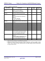
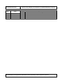
the same as expected. Table 1.1 shows Peripheral Functions and Their Applications
Table 1.1
Peripheral Functions and Their Applications
Peripheral functions
DISCOM
INTC (interrupt ID: CMP1 (129))
VDC5 (ch1) (layer 2)
R01AN1825EJ0100
May 27, 2014
Rev.1.00
Application
Compares CRC codes for graphics data.
Controls an interrupt due to discrepancy detection by
display out comparison.
Displays an image on the LCD.
Page 3 of 28
RZ/A1H Group
2.
Display Out Comparison Unit(DISCOM)Sample Program
Operation Check Conditions
The sample code accompanying this application note has been run and confirmed under the conditions
below.
Table 2.1
Operation Check Conditions
Item
Contents
MCU used
Operating frequency*
RZ/A1H
Operating voltage
Integrated development
environment
C compiler
Operating mode
CPU clock (Iφ): 400MHz
Image processing clock (Gφ): 266.67MHz
Internal bus clock (Bφ): 133.33MHz
Peripheral clock 1 (P1φ): 66.67MHz
Peripheral clock 0 (P0φ): 33.33MHz
Power supply voltage (I/O): 3.3V
Power supply voltage (Internal): 1.18V
ARM® integrated development environment
ARM Development Studio 5 (DS-5TM) Version 5.16
ARM C/C++ Compiler/Linker/Assembler Ver.5.03 [Build 102]
Compiler options (excluding additional directory path)
-O3 -Ospace --cpu=Cortex-A9 --littleend --arm --apcs=/interwork
--no_unaligned_access --fpu=vfpv3_fp16 -g --asm
Boot mode 0
(CS0-space 16-bit booting)
Board used
GENMAI board
・RTK772100BC00000BR (R7S72100 CPU board)
・RTK7721000B00000BR (Option board for the R7S72100 CPU board)
Device used (functionality to be
used on the board)
Display Out (Analog RGB D-sub15) (Option board :J15)
Serial interface (connected with a Dsub-9 connector)
Note: * The operating frequency used in clock mode 0 (Clock input of 13.33MHz from EXTAL pin)
R01AN1825EJ0100
May 27, 2014
Rev.1.00
Page 4 of 28
RZ/A1H Group
3.
Display Out Comparison Unit(DISCOM)Sample Program
Related Application Notes
For additional information associated with this document, refer to the following application note.
RZ/A1H Group Example of Initialization (R01AN1864EJ)
RZ/A1H Group Video Display Controller 5 Sample Driver(R01AN1822EJ)
RZ/A1H Group I/O definition header file <iodefine.h> (R01AN1860EJ)
4.
Peripheral Functions
The basic functions of the CEU and VDC5 are described in the RZ/A1H Group User’s Manual: Hardware.
R01AN1825EJ0100
May 27, 2014
Rev.1.00
Page 5 of 28
RZ/A1H Group
5.
5.1
Display Out Comparison Unit(DISCOM)Sample Program
Hardware
Hardware Configuration
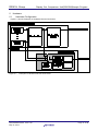
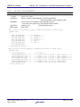
Figure 5.1 shows Examples of Hardware Devices Connected.
Figure 5.1
Examples of Hardware Devices Connected
R01AN1825EJ0100
May 27, 2014
Rev.1.00
Page 6 of 28
RZ/A1H Group
6.
Display Out Comparison Unit(DISCOM)Sample Program
Software
6.1
Operational Overview
This sample program checks through the DISCOM whether graphics data from graphics display module
VDC5 is the same as expected.
The screen displayed by the VDC5 is refreshed at fixed intervals. Each time it is refreshed, its data is
compared by using the DISCOM. The CRC codes for comparison of data on the screen are calculated in
software and set in the DISCOM. The DISCOM is also available to calculate the CRC codes. If the compared
data does not match, a discrepancy is detected upon a DISCOM interrupt due to discrepancy detection by
display out comparison. The comparison results are serially output.
6.1.1
Serial output
Below is output serial data. CRC values are enclosed in parentheses.
The bit rate for serial data transmission is 115,200 bps.
RZ/A1H CPU Board Sample Program. Ver.1.00
Copyright (C) 2013 Renesas Electronics Corporation. All rights reserved.
_/_/_/_/
Aragon Discom Sample Ver.1.00
_/_/_/_/
CRC OK (0x209C86E3)
CRC OK (0x571E9393)
CRC OK (0x0E34838C)
CRC OK (0xC4F7C315)
CRC OK (0x5278291D)
CRC OK (0x98BB6984)
CRC OK (0xC191799B)
CRC OK (0x2B4702B4)
CRC OK (0xD3E181F3)
CRC OK (0x9DDDD30A)
CRC OK (0xBDB85D8F)
CRC OK (0x0B523902)
CRC OK (0xA7833023)
Figure 6.1
Output from the DISCOM
R01AN1825EJ0100
May 27, 2014
Rev.1.00
Page 7 of 28
RZ/A1H Group
6.2
Display Out Comparison Unit(DISCOM)Sample Program
Memory Mapping
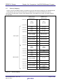
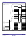
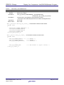
Figure 6.2 shows the Address Space of the RZ/A1H group and the Memory Mapping of the GENMAI board.
In this sample code, the code and data used in the ROM area is located in the NOR flash memory
connected to the CS0 space, and the code and data used in the RAM area is located in the large-capacity
on-chip RAM.
RZ/A1H group
Address space
GENMAI board
Memory map
Others
(2550MB)
Others
(2550MB)
Large-capacity on-chip RAM
(10MB)
Large-capacity on-chip RAM
mirror space
SPI multi I/O bus space 2
(64MB)
SPI multi I/O bus
mirror space 2
SPI multi I/O bus space 1
(64MB)
SPI multi I/O bus
mirror space 1
CS5 space (64MB)
CS4 space (64MB)
CS5 mirror space
CS4 mirror space
CS3 space (64MB)
CS3 mirror space
CS2 space (64MB)
CS2 mirror space
CS1 space (64MB)
CS1 mirror space
CS0 space (64MB)
CS0 mirror space
Others
(502MB)
Others
(502MB)
Large-capacity on-chip RAM
(10MB)
Large-capacity on-chip RAM
(10MB)
SPI multi I/O bus space 2
(64MB)
Serial flash memory (64MB)
SPI multi I/O bus space 1
(64MB)
Serial flash memory (64MB)
CS5 space (64MB)
CS4 space (64MB)
User area
CS3 space (64MB)
SDRAM (64MB)
CS2 space (64MB)
SDRAM (64MB)
CS1 space (64MB)
NOR flash memory
(64MB)
CS0 space (64MB)
NOR flash memory
(64MB)
H'FFFF FFFF
H'60A0 0000
H'6000 0000
H'5C00 0000
H'5800 0000
Mirror space
H'5000 0000
H'4C00 0000
H'4800 0000
H'4400 0000
H'4000 0000
H'20A0 0000
H'2000 0000
H'1C00 0000
H'1800 0000
Normal space
H'1000 0000
H'0C00 0000
H'0800 0000
H'0400 0000
H'0000 0000
Figure 6.2
Memory Mapping
R01AN1825EJ0100
May 27, 2014
Rev.1.00
Page 8 of 28
RZ/A1H Group
6.2.1
Display Out Comparison Unit(DISCOM)Sample Program
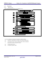
Section Assignment in Sample Code
In this sample code, the exception processing vector table and the IRQ interrupt handler are assigned to the
large-capacity on-chip RAM, and they are executed in such RAM to speed up the interrupt processing. The
transfer processing from the NOR flash memory area which is the program code of the exception processing
vector table and the IRQ interrupt handler to the large-capacity on-chip RAM area, the clear to zero
processing for the data selection without initial data, and the initialization for the data selection with initial data
are executed by using the scatter-loading function. Refer to "Image structure and generation" in "ARM
Compiler toolchain Using the Linker" provided by the ARM for more information about the scatter-loading
function.
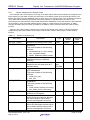
Table 6.1 and Table 6.2 list the Sections to be Used in this sample code. Figure 6.3 shows the Section
Assignment for the initial condition of the sample code and the condition after using the scatter-loading
function.
Table 6.1
Sections to be Used (1/2)
Area Name
VECTOR_TABLE
RESET_HANDLER
Description
Exception processing vector table
Program code area of reset handler
processing
This area consists of the following
sections.
Type
Code
Code
Loading
Area
FLASH
FLASH
Execution
Area
FLASH
FLASH
Code
FLASH
FLASH
Code
and
RO Data
Code
FLASH
FLASH
FLASH
FLASH
Code
FLASH
FLASH
Code
FLASH
FLASH
Code
FLASH
FLASH
RO Data
FLASH
FLASH
• INITCA9CACHE (L1 cache setting)
• INIT_TTB (MMU setting)
• RESET_HANDLER (Reset handler)
CODE_BASIC_SETUP Program code area to optimize
operating frequency and flash
memory
InRoot
This area consists of the sections
located in the root area such as C
standard library.
CODE_FPU_INIT
Program code area for NEON and
VFP initializations
This area consists of the following
sections.
• CODE_FPU_INIT
• FPU_INIT
CODE_RESET
Program code area for hardware
initialization
This area consists of the following
sections.
• CODE_RESET (Startup processing)
• INIT_VBAR (Vector base setting)
CODE_IO_REGRW
CODE
CONST
R01AN1825EJ0100
May 27, 2014
Program code area for read/write
functions of I/O register
Program code area for defaults
All the Code type sections which do
not define section names with C
source are assigned in this area.
Constant data area for defaults
All the RO Data type sections which
do not define section names with C
source are assigned in this area.
Rev.1.00
Page 9 of 28
RZ/A1H Group
Table 6.2
Display Out Comparison Unit(DISCOM)Sample Program
Sections to be Used (2/2)
Area Name
Description
VECTOR_MIRROR_ Exception processing vector table
TABLE
(Section to transfer data to
large-capacity on-chip RAM)
CODE_HANDLER_
Program code area for user-defined
functions of IRQ interrupt handler
JMPTBL
CODE_HANDLER
Program code area of IRQ interrupt
handler
This area consists of the following
sections.
Type
Code
Loading
Area
FLASH
Execution
Area
LRAM
Code
FLASH
LRAM
Code
FLASH
LRAM
RW Data
FLASH
LRAM
ZI Data
ZI Data
ZI Data
ZI Data
ZI Data
ZI Data
ZI Data
RW Data
FLASH
LRAM
LRAM
LRAM
LRAM
LRAM
LRAM
LRAM
LRAM
ZI Data
-
LRAM
Data
-
LRAM
• CODE_HANDLER
• IRQ_FIQ_HANDLER
DATA_HANDLER_
JMPTBL
ARM_LIB_STACK
IRQ_STACK
FIQ_STACK
SVC_STACK
ABT_STACK
TTB
ARM_LIB_HEAP
DATA
BSS
VRAM
Registration table data area for
user-defined functions of IRQ interrupt
handler
Application stack area
IRQ mode stack area
FIQ mode stack area
Supervisor (SVC) mode stack area
Abort (ABT) mode stack area
MMU translation table area
Application heap area
Data area with initial value for defaults
All the RW Data type sections which
do not define section names with C
source are assigned in this area.
Data area without initial value for
defaults
All the ZI Data type sections which do
not define section names with C
source area assigned in this area.
Display Buffer
Notes: 1. "FLASH" and "LRAM" shown in Loading Area and Execution Area indicate the NOR flash memory
area and the large-capacity on-chip RAM area respectively.
2. Basically the section name is set to be the same as the region's, however it consists of some
sections in the areas of RESET_HANDLER, InRoot, CODE_FPU_INIT, CODE_RESET, CODE,
CONST, CODE_HANDLER, DATA, and BSS. Refer to the ARM compiler toolchain manual about
the region and the section.
R01AN1825EJ0100
May 27, 2014
Rev.1.00
Page 10 of 28
RZ/A1H Group
Display Out Comparison Unit(DISCOM)Sample Program
RZ/A1H group
Address space
H'FFFF FFFF
Section assignment
(Load view)
Section assignment
(Execution view)
Memory allocation after
executing scatter-loading
H'209F FFFF
Clear to zero
BSS
Initialize data
with initial value
DATA
H'200B 8000
ARM_LIB_HEAP
H'2003 8000
Secure area such
as stack area
H'2003 4000
H'2003 2000
H'2003 0000
H'2002 E000
H'2002 C000
TTB
ABT_STACK
SVC_STACK
FIQ_STAC
IRQ_STACK
ARM_LIB_STACK
H'2002 4000
Initialize data
with initial value
DATA_HANDLER_JMPTBL
CODE_HANDLER
H'2002 0100
CODE_HANDLER_JMPTBL
H'2002 0000
VECTOR_MIRROR_TABLE
H'2000 0000
H'03FF FFFF
H'4000 0000
DATA
DATA_HANDLER_JMPTBL
H'20A0 0000
H'2000 0000
CODE_HANDLER
Large-capacity on-chip RAM
(10MB)
CODE_HANDLER_JMPTBL
CONST
H'1C00 0000
CODE
CODE_IO_REGRW
H'1800 0000
H'1000 0000
H'0C00 0000
H'0800 0000
Figure 6.3
CS0 space
(64MB)
CODE
CODE_IO_REGRW
CODE_RESET
CODE_RESET
CODE_FPU_INIT
InRoot
InRoot
CODE_BASIC_SETUP
CODE_BASIC_SETUP
RESER_HANDLER
H'0400 0000
CONST
CODE_FPU_INIT
H'0000 0200
H'0000 0000
Transfer program
code which requires
speeding up to onchip RAM
H'0000 0100
VECTOR_MIRROR_TABLE
H'0000 0000
VECTOR_TABLE
Transfer exception
processing vector to
on-chip RAM
RESER_HANDLER
VECTOR_TABLE
Section Assignment
R01AN1825EJ0100
May 27, 2014
Rev.1.00
Page 11 of 28
RZ/A1H Group
6.2.2
Display Out Comparison Unit(DISCOM)Sample Program
MMU settings
The MMU is set to manage the 4 GB area in 1MB unit from the address H'0000 0000 in response to the
memory map of the hardware resource used for the GENMAI board. (Set by the ttb_init.s file.) The minimum
unit should be 1MB when customizing the MMU based on the system.
Table 6.3 lists the Setting for MMU.
Table 6.3
Setting for MMU
Definition Name
M_SIZE_NOR
Contents
CS0 and CS1 spaces
(NOR flash memory)
M_SIZE_SDRAM
CS2 and CS3 spaces
(SDRAM)
M_SIZE_CS45
CS4 and CS5 spaces
M_SIZE_SPI
SPI multi IO bus
space 1 and 2
(serial flash memory)
Large-capacity on-chip
RAM space
M_SIZE_RAM
M_SIZE_IO_1
On-chip peripheral
module and reserved
area
M_SIZE_NOR_M
CS0 and CS1 mirror
spaces
M_SIZE_SDRAM_M
CS2 and CS3 mirror
spaces
M_SIZE_CS45_M
CS4 and CS5 mirror
spaces
M_SIZE_SPI_M
SPI multi IO bus
mirror space 1 and 2
M_SIZE_RAM_M
Large-capacity on-chip
RAM mirror space
M_SIZE_IO_2
On-chip peripheral
module and reserved
area
R01AN1825EJ0100
May 27, 2014
Rev.1.00
Address
H'0000 0000
to
H'07FF FFFF
H'0800 0000
to
H'0FFF FFFF
H'1000 0000
to
H'17FF FFFF
H'1800 0000
to
H'1FFF FFFF
H'2000 0000
to
H'209F FFFF
H'20A0 0000
to
H'3FFF FFFF
H'4000 0000
to
H'47FF FFFF
H'4800 0000
to
H'4FFF FFFF
H'5000 0000
to
H'57FF FFFF
H'5800 0000
to
H'5FFF FFFF
H'6000 0000
to
H'609F FFFF
H'60A0 0000
to
H'FFFF FFFF
Size
128MB
Memory Type
L1 cache enable,
Normal memory
128MB
L1 cache enable,
Normal memory
128MB
Strongly-ordered memory
(L1 cache disable)
128MB
L1 cache enable,
Normal memory
10MB
L1 cache enable,
Normal memory
502MB
Strongly-ordered memory
(L1 cache disable)
128MB
L1 cache disable,
Normal memory
128MB
L1 cache disable,
Normal memory
128MB
Strongly-ordered memory
(L1 cache disable)
128MB
L1 cache disable,
Normal memory
10MB
L1 cache disable,
Normal memory
2550MB
Strongly-ordered memory
(L1 cache disable)
Page 12 of 28
RZ/A1H Group
6.3
Display Out Comparison Unit(DISCOM)Sample Program
Interrupts
Table 6.4 shows interrupts for the sample code.
Table 6.4
Interrupts for the Sample Code
Interrupt (factor ID)
CMP1
GR3_VLINE1
6.4
Priority
5
5
Process outline
Interrupt due to discrepancy detection by display out
comparison
Line signal specified for graphics (3) panel output
Basic Data Types
Table 6.5 shows the basic data types for the sample code.
Table 6.5
Basic Data Types for the Sample Code
Symbol
char_t
bool_t
int_t
int8_t
int16_t
int32_t
int64_t
uint8_t
uint16_t
uint32_t
uint64_t
float32_t
float64_t
float128_t
R01AN1825EJ0100
May 27, 2014
Rev.1.00
Contents
8-bit character
Boolean type, value: true (1) or false (0)
High-speed integer, signed
32-bit integer in this sample code
8-bit integer, singed (Defined by standard library)
16-bit integer, singed (Defined by standard library)
32-bit integer, singed (Defined by standard library)
64-bit integer, singed (Defined by standard library)
8-bit integer, unsigned (Defined by standard library)
16-bit integer, unsigned (Defined by standard library)
32-bit integer, unsigned (Defined by standard library)
64-bit integer, unsigned (Defined by standard library)
32-bit floating point
(Defined by standard library when specifying "__ARM_NEON__")
64-biy floating point (Defined by standard library)
(Defined by standard library when specifying "__ARM_NEON__")
128-bit floating point
Page 13 of 28
RZ/A1H Group
6.5
Display Out Comparison Unit(DISCOM)Sample Program
List of Constants and Error Codes
Table 6.6 lists the constants for the sample program. Table 6.7 lists the error codes for the sample code.
Table 6.6
Constants for the Sample Program
Constant
Setting
DISCOM_CHANNEL_0
DISCOM_CHANNEL_1
DISCOM_OFF
DISCOM_ON
DISCOM_PIX_FORMAT_ARGB8888
DISCOM_PIX_FORMAT_RGB888
DISCOM_PIX_FORMAT_RGB565
DISCOM_CMPSELP_NO
DISCOM_CMPSELP_1_GR0
DISCOM_CMPSELP_2_GR1
DISCOM_CMPSELP_3_GR2
DISCOM_CMPSELP_4_GR3
DISCOM_CMPSELP_5_OIR
DISCOM_CMPSELP_AB
Table 6.7
0
1
0
1
0
1
2
0
1
2
3
4
5
6
Description
DISCOM channel 0
DISCOM channel 1
Off
On
Pixel format ARGB8888
Pixel format RGB888
Pixel format RGB565
Not selected.
Graphics (0)
Graphics (1)
Graphics (2)
Graphics (3)
Graphics (OIR)
Graphics data after α blending
Error Codes for the Sample Code
Constant
Setting
DISCOM_OK
DISCOM_ERR_PARAM_CHANNEL
0
1
DISCOM_ERR_PARAM_BIT_WIDTH
2
DISCOM_ERR_PARAM_UNDEFINED
DISCOM_ERR_PARAM_NULL
DISCOM_ERR_UPDATE_TIMING
3
4
5
DISCOM_ERR_STATUS
6
R01AN1825EJ0100
May 27, 2014
Rev.1.00
Description
Normal completion
Parameter error: The specified channel number is
not correct.
Parameter error: The specified value is greater than
the bit-width of the parameter.
Parameter error: The specified value is not defined.
Parameter error: Null cannot be set to the pointer.
Timing error: The updating registers in this timing
causes an unexpected result in the CRC code
calculation.
Status error: Calling the API function is not allowed
in the status.
Page 14 of 28
RZ/A1H Group
6.6
Display Out Comparison Unit(DISCOM)Sample Program
List of Variables
Table 6.8 lists the static variables.
Table 6.8
Type
Variable Name
int32_t
6.7
Static Variables
crc_error
Contents
DISCOM interrupt detection flag
Function Used
CrcErrorDetection ()
List of Functions
Table 6.9 lists the list of functions.
Table 6.9
List of Functions
Function name
Page number
R_DISCOM_Initialize
R_DISCOM_Terminate
16
16
R_DISCOM_Configure
R_DISCOM_SetInterrupt
R_DISCOM_Start
R_DISCOM_Stop
R_DISCOM_GetCRC
DiscomDrv_Init
DiscomDrv_Term
DiscomDrv_ConvChannel
DiscomDrv_ConvGrTypeSelPlanel
DiscomDrv_ConvPixRdFormat
DiscomDrv_CalcCRC
17
19
19
19
20
20
20
21
22
23
24
R01AN1825EJ0100
May 27, 2014
Rev.1.00
Page 15 of 28
RZ/A1H Group
6.8
Display Out Comparison Unit(DISCOM)Sample Program
Function Specifications
This section contains the specifications for the functions that are implemented in the sample code.
6.8.1
R_DISCOM_Initialize
R_DISCOM_Initialize
Synopsis
DISCOM driver initialization.
Header
r_discom.h
Declaration
discom_error_t R_DISCOM_Initialize(
const discom_channel_t ch,
void (* const init_func)(uint32_t),
const uint32_t user_num)
Description
In this function, the operations are performed as below.
- The specified user-defined function is executed.
- The DISCOM driver internal variables are initialized.
- The operation of the panel clock is enabled.
Arguments
ch
:Channel
init_func
:Pointer to the user-defined function
user_num
:User-defined number
Return value
Error code
6.8.2
R_DISCOM_Terminate
R_DISCOM_Terminate
Synopsis
DISCOM driver termination.
Header
r_discom.h
Declaration
discom_error_t R_DISCOM_Terminate(
const discom_channel_t ch,
void (* const quit_func)(uint32_t),
const uint32_t user_num)
Description
In this function, the operations are performed as below.
- The specified user-defined function is executed.
- Stop the interrupt of DISCOM.
Arguments
ch
:Channel
quit_func
:Pointer to the user-defined function
user_num
:User-defined number
Return value
Error code
R01AN1825EJ0100
May 27, 2014
Rev.1.00
Page 16 of 28
RZ/A1H Group
6.8.3
Display Out Comparison Unit(DISCOM)Sample Program
R_DISCOM_Configure
R_DISCOM_Configure
Synopsis
DISCOM driver configuration.
Header
r_discom.h
Declaration
discom_error_t R_DISCOM_Configure(
const discom_channel_t ch,
const discom_config_t * const config,
const discom_rect_area_t * const rect_area)
Description
In this function, the operations are performed as below.
- Operation Parameter Setting.
- Setting the rectangular area for which the CRC code is calculated.
Arguments
ch
: Channel
config
: Operation Parameter Setting
rect_area
: Rectangular area for which the CRC code is calculated
Return value
Error code
The discom_config_t structure members are shown below.
typedef struct
{
discom_pix_format_t pix_format;
uint8_t
cmpdfa;
discom_onoff_t
cmpdauf;
discom_cmpselp_t
cmpselp;
} discom_config_t;
Type
Argument name
discom_pix_format_t
pix_format
Input/ou
tput
in
uint8_t
cmpdfa
discom_onoff_t
cmpdauf
in
discom_cmpselp_tdly
cmpselp
in
R01AN1825EJ0100
May 27, 2014
in
Rev.1.00
Description
Pixel format
• DISCOM_PIX_FORMAT_ARGB8888: ARGB8888
• DISCOM_PIX_FORMAT_RGB888: RGB888
• DISCOM_PIX_FORMAT_RGB565: RGB565
Default α value for display out comparison
Specifies whether to use the default α value for display out
comparison.
• DISCOM_OFF: Does not use the default α value.
• DISCOM_ON: Uses the default α value.
Plane selected for display out comparison
• DISCOM_CMPSELP_NO:
• DISCOM_CMPSELP_1_GR0: Graphics (0)
• DISCOM_CMPSELP_2_GR1: Graphics (1)
• DISCOM_CMPSELP_3_GR2: Graphics (2)
• DISCOM_CMPSELP_4_GR3: Graphics (3)
• DISCOM_CMPSELP_5_OIR: Graphics (OIR)
• DISCOM_CMPSELP_AB: Graphics data after α blending
Page 17 of 28
RZ/A1H Group
Display Out Comparison Unit(DISCOM)Sample Program
The discom_rect_area_t structure members are shown below.
typedef struct
{
uint16_t
cmpspx;
uint16_t
cmpspy;
uint16_t
cmpszx;
uint16_t
cmpszy;
} discom_rect_area_t;
Type
Argument name
uint16_t
cmpspx
Input/output
in
uint16_t
cmpspy
in
uint16_t
cmpszx
in
uint16_t
cmpszy
in
R01AN1825EJ0100
May 27, 2014
Rev.1.00
Description
Horizontal start position for display out comparison
Specifies the horizontal start position of the rectangular area for
which the CRC code should be calculated. Set a value smaller
than or equal to the horizontal size of graphics data.
Vertical start position for display out comparison.
Specifies the vertical start position of the rectangular area for
which the CRC code should be calculated. Set a value smaller
than or equal to the vertical size of graphics data.
Horizontal size for display out comparison
Specifies the horizontal size of the rectangular area for which the
CRC code should be calculated. Set a value so the horizontal
size of graphics data can be as follows.
Horizontal size of graphics data ≥ Horizontal start position
(cmpspx) + Horizontal size (cmpszx)
Vertical size for display out comparison
Specifies the vertical size of the rectangular area for which the
CRC code should be calculated. Set a value so the vertical size
of graphics data can be as follows.
Vertical size of graphics data ≥ Vertical start position (cmpspy) +
Vertical size (cmpszy)
Page 18 of 28
RZ/A1H Group
6.8.4
Display Out Comparison Unit(DISCOM)Sample Program
R_DISCOM_SetInterrupt
R_DISCOM_SetInterrupt
Synopsis
DISCOM driver set ISR.
Header
r_discom.h
Declaration
discom_error_t R_DISCOM_SetInterrupt(
const discom_channel_t ch,
void (* const callback)(void))
Description
In this function, the operations are performed as below.
- Setting the interrupt of DISCOM.
- Setting the callback function.
Arguments
ch
: Channel
callback
: Pointer to the user-defined function
Return value
Error code
6.8.5
R_DISCOM_Start
R_DISCOM_Start
Synopsis
Header
Declaration
Description
Arguments
Return value
6.8.6
DISCOM driver start.
r_discom.h
discom_error_t R_DISCOM_Start(
const discom_channel_t ch,
const uint32_t cmpecrc)
In this function, the operations are performed as below.
- Start DISCOM.
- Setting the CRC code to compare.
ch
: Channel
cmpecrc
: Expected display out comparison CRC code
Error code
R_DISCOM_Stop
R_DISCOM_Stop
Synopsis
Header
Declaration
Description
Arguments
Return value
R01AN1825EJ0100
May 27, 2014
DISCOM driver stop.
r_discom.h
discom_error_t R_DISCOM_Stop(
const discom_channel_t ch)
In this function, the operations are performed as below.
- Stop DISCOM.
ch
: Channel
Error code.
Rev.1.00
Page 19 of 28
RZ/A1H Group
6.8.7
Display Out Comparison Unit(DISCOM)Sample Program
R_DISCOM_GetCRC
R_DISCOM_GetCRC
Synopsis
T DISCOM driver get CRC code.
Header
r_discom.h
Declaration
discom_error_t R_DISCOM_GetCRC(
const discom_channel_t ch,
const uint32_t * crc_code);
Description
In this function, the operations are performed as below.
- Get CRC code.
Arguments
ch
: Channel
crc_code
: CRC code
Return value
Error code.
6.8.8
DiscomDrv_Init
DiscomDrv_Init
Synopsis
Header
Declaration
Description
Arguments
Return value
6.8.9
DISCOM driver initialization.
discom_drv_utility.h
discom_error_t DISCOMDRV _Init(
const discom_channel_t channel,
void (* const IntCallbackFunc)(void))
In this function, the operations are performed as below.
- Call the function (R_DISCOM_Initialize).
- Call the function (R_DISCOM_SetInterrupt).
channel
: Channel
IntCallbackFunc
: Pointer to the user-defined function
Error code.
DiscomDrv_Term
DiscomDrv_Term
Synopsis
Header
Declaration
Description
Arguments
Return value
R01AN1825EJ0100
May 27, 2014
DISCOM driver termination.
discom_drv_utility.h
discom_error_t DISCOMDRV _Term(
const discom_channel_t channel)
In this function, the operations are performed as below.
- Call the function (R_DISCOM_Terminate).
- Call the function (R_DISCOM_SetInterrupt).
channel
: Channel
Error code.
Rev.1.00
Page 20 of 28
RZ/A1H Group
6.8.10
Display Out Comparison Unit(DISCOM)Sample Program
DiscomDrv_ConvChannel
DiscomDrv_ConvChannel
Synopsis
Conversion channel.
Header
discom_drv_utility.h
Declaration
discom_channel_t DiscomDrv_ConvChannel (vdc5_channel_t channel)
Description
In this function, the operations are performed as below.
- Conversion from VDC5 channel into DISCOM channel.
Arguments
channel
: Channel
Return value
Error code.
The r_vdc5.h vdc5_channel_t
/*! Channel */
typedef enum
{
VDC5_CHANNEL_0 = 0,
VDC5_CHANNEL_1,
VDC5_CHANNEL_NUM
} vdc5_channel_t;
enumeration method is shown below.
/*!< VDC5 channel 0 */
/*!< VDC5 channel 1 */
/*!< The number of VDC5 channels */
r_discom.h discom_channel_t enumeration method is shown below.
typedef enum
{
DISCOM_CHANNEL_0 = 0,
/*!< DISCOM channel 0 */
DISCOM_CHANNEL_1,
/*!< DISCOM channel 1 */
DISCOM_CHANNEL_NUM
/*!< The number of DISCOM channels */
} discom_channel_t;
R01AN1825EJ0100
May 27, 2014
Rev.1.00
Page 21 of 28
RZ/A1H Group
6.8.11
Display Out Comparison Unit(DISCOM)Sample Program
DiscomDrv_ConvGrTypeSelPlanel
DiscomDrv_ConvGrTypeSelPlanel
Synopsis
Conversion plane.
Header
discom_drv_utility.h
Declaration
discom_cmpselp_t DISCOMDRV_ConvGrTypeSelPlane(
const vdc5_graphics_type_t graphics_type)
Description
In this function, the operations are performed as below.
- Conversion from graphics type into DISCOM selection plane.
Arguments
graphics_type
: VDC5 Graphics type ID
Return value
Error code.
The r_vdc5.h vdc5_graphics_type_t enumeration method is shown below.
typedef enum
{
VDC5_GR_TYPE_GR0 = 0, /*!< Graphics 0 */
VDC5_GR_TYPE_GR1,
/*!< Graphics 1 */
VDC5_GR_TYPE_GR2,
/*!< Graphics 2 */
VDC5_GR_TYPE_GR3,
/*!< Graphics 3 */
VDC5_GR_TYPE_VIN,
/*!< VIN */
VDC5_GR_TYPE_OIR,
/*!< OIR */
VDC5_GR_TYPE_NUM
} vdc5_graphics_type_t;
The r_discom.h discom_cmpselp_t enumeration method is shown below.
typedef enum
{
DISCOM_CMPSELP_NO
= 0, /*!< No data */
DISCOM_CMPSELP_1_GR0 = 1, /*!< Graphics data of plane 1 (VDC5 graphics
DISCOM_CMPSELP_2_GR1 = 2, /*!< Graphics data of plane 2 (VDC5 graphics
DISCOM_CMPSELP_3_GR2 = 3, /*!< Graphics data of plane 3 (VDC5 graphics
DISCOM_CMPSELP_4_GR3 = 4, /*!< Graphics data of plane 4 (VDC5 graphics
DISCOM_CMPSELP_5_OIR = 5, /*!< Graphics data of plane 5 (VDC5 OIR)*/
DISCOM_CMPSELP_AB
= 9
/*!< Graphics data after alpha blending */
} discom_cmpselp_t;
R01AN1825EJ0100
May 27, 2014
Rev.1.00
0)
1)
2)
3)
*/
*/
*/
*/
Page 22 of 28
RZ/A1H Group
6.8.12
Display Out Comparison Unit(DISCOM)Sample Program
DiscomDrv_ConvPixRdFormat
DiscomDrv_ConvPixRdFormat
Synopsis
Conversion signal format
Header
discom_drv_utility.h
Declaration
vdc5_gr_format_t DISCOMDRV _ConvPixRdFormat(
const discom_pix_format_t pix_format)
Description
In this function, the operations are performed as below.
- Conversion from DISCOM pixel format into VDC5 read signal format.
Arguments
pix_format
Return value
Error code.
The r_discom.h discom_pix_format_t enumeration method is shown below.
typedef enum
{
DISCOM_PIX_FORMAT_ARGB8888 = 0,
DISCOM_PIX_FORMAT_RGB888,
DISCOM_PIX_FORMAT_RGB565,
DISCOM_PIX_FORMAT_NUM
} discom_pix_format_t;
The r_vdc5.h vdc5_gr_format_t
typedef enum
{
VDC5_GR_FORMAT_RGB565 = 0,
VDC5_GR_FORMAT_RGB888,
VDC5_GR_FORMAT_ARGB8888,
・
・
VDC5_GR_FORMAT_NUM
} vdc5_gr_format_t;
R01AN1825EJ0100
May 27, 2014
Rev.1.00
enumeration method is shown below.
/*!< RGB565 */
/*!< RGB888 */
/*!< ARGB8888 */
/*!< The number of signal formats */
Page 23 of 28
RZ/A1H Group
6.8.13
Display Out Comparison Unit(DISCOM)Sample Program
DiscomDrv_CalcCRC
DiscomDrv_CalcCRC
Synopsis
Crc calculate
Header
discom_drv_utility.h
Declaration
uint32_t DISCOMDRV _CalcCRC (
void
* const framebuff,
const uint32_t
fb_stride,
const discom_pix_format_t
pix_format,
const uint32_t
crc_ini,
const discom_rect_area_t
* const rect_area)
Description
In this function, the operations are performed as below.
-CRC calculation of the rect area.
Arguments
framebuff
: buffer pointer
fb_stride
: buffer stride
pix_format
: pixel format
crc_ini
: The initial value of the CRC
rect_area
: The rect area for CRC calculation
Return value
Crc code
R01AN1825EJ0100
May 27, 2014
Rev.1.00
Page 24 of 28
RZ/A1H Group
6.9
Display Out Comparison Unit(DISCOM)Sample Program
Flowcharts
6.9.1
Main process
shows main process described in this application note.
Figure 6.4
Main Process
(1) to (4): Initialize the VDC5 and configure the display settings.
(5)
: Initialize the DISCOM and configure the operation parameters.
(6)
: Calculate the CRC codes for graphics data, start the DISCOM,
and check the CRC comparison results.
(7)
: Create graphics data.
(8)
: Change the graphics data.
R01AN1825EJ0100
May 27, 2014
Rev.1.00
Page 25 of 28
RZ/A1H Group
6.9.2
Display Out Comparison Unit(DISCOM)Sample Program
Process of detecting a CRC error through the DISCOM
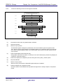
CrcErrorDetection
(1)
DiscomDrv_CalcCRC
(2)
R_DISCOM_Start
(3)
WaitVsync(2)
(4)
(5)
crc_error = 0;
WaitVsync(VSYNC_WAIT_COUNT)
(6)
R_DISCOM_Stop
(7)
WaitVsync(1)
(8)
result output
End
Figure 6.5
CRC Error Detection through the DISCOM
(1)
: Calculate the CRC codes for graphics data in software.
(2)
: Start the DISCOM.
(3)
: Wait two Vsync periods.
The DISCOM register settings are updated at the end of the effective period of graphics data.
Thus, wait one Vsync period until they are updated. Display out comparison starts upon detection
of the start of effective graphics data. Thus, wait another Vsync period. The total wait time is two
Vsync periods.
(4)
: Clear the DISCOM interrupt detection flag.
If the graphics data does not match, an interrupt occurs due to discrepancy detection by display out
comparison, setting this flag to 1.
(5)
: Perform the display out comparison process during the VSYN_WAIT_COUNT period.
(6)
: Stop the DISCOM.
(7)
: Wait one Vsync period.
Wait one Vsync period until the DISCOM register settings are updated.
(8)
: Output the display out comparison results.
Check the status of the DISCOM interrupt detection flag and then serially output the comparison
results.
R01AN1825EJ0100
May 27, 2014
Rev.1.00
Page 26 of 28
RZ/A1H Group
7.
Display Out Comparison Unit(DISCOM)Sample Program
Sample Code
The sample code is available on the Renesas Electronics Website.
8.
Documents for Reference
User's Manual: Hardware
RZ/A1H Group User's Manual: Hardware
The latest version can be downloaded from the Renesas Electronics website.
R7S72100 RTK772100BC00000BR (GENMAI) User's Manual
The latest version can be downloaded from the Renesas Electronics website.
R7S72100 CPU (GENMAI) Optional Board RTK7721000B00000BR User's Manual
The latest version can be downloaded from the Renesas Electronics website.
ARM Architecture Reference Manual ARMv7-A and ARMv7-R edition Issue C
The latest version can be downloaded from the ARM website.
ARM Generic Interrupt Controller Architecture Specification Architecture version 1.0
The latest version can be downloaded from the ARM website.
Technical Update/Technical News
The latest information can be downloaded from the Renesas Electronics website.
User's Manual: Development Tools
ARM Software Development Tools (ARM Compiler toolchain, ARM DS-5 etc) can be downloaded from the ARM
website.
The latest version can be downloaded from the Renesas Electronics website.
R01AN1825EJ0100
May 27, 2014
Rev.1.00
Page 27 of 28
RZ/A1H Group
Display Out Comparison Unit(DISCOM)Sample Program
Website and Support
Renesas Electronics website
http://www.renesas.com
Inquiries
http://www.renesas.com/contact/
R01AN1825EJ0100
May 27, 2014
Rev.1.00
Page 28 of 28
REVISISON HISTORY
Rev.
Date
1.00
May 27,2014
RZ/A1H Group Display Out Comparison Unit(DISCOM)Sample Program
Description
Summary
ページ
—
First edition issued
All trademarks and registered trademarks are the property of their respective owners.
General Precautions in the Handling of MPU/MCU Products
The following usage notes are applicable to all MPU/MCU products from Renesas. For detailed usage notes on the
products covered by this document, refer to the relevant sections of the document as well as any technical updates that
have been issued for the products.
1. Handling of Unused Pins
Handle unused pins in accordance with the directions given under Handling of Unused Pins in the
manual.
The input pins of CMOS products are generally in the high-impedance state. In operation with an
unused pin in the open-circuit state, extra electromagnetic noise is induced in the vicinity of LSI, an
associated shoot-through current flows internally, and malfunctions occur due to the false
recognition of the pin state as an input signal become possible. Unused pins should be handled as
described under Handling of Unused Pins in the manual.
2. Processing at Power-on
The state of the product is undefined at the moment when power is supplied.
The states of internal circuits in the LSI are indeterminate and the states of register settings and
pins are undefined at the moment when power is supplied.
In a finished product where the reset signal is applied to the external reset pin, the states of pins are
not guaranteed from the moment when power is supplied until the reset process is completed.
In a similar way, the states of pins in a product that is reset by an on-chip power-on reset function
are not guaranteed from the moment when power is supplied until the power reaches the level at
which resetting has been specified.
3. Prohibition of Access to Reserved Addresses
Access to reserved addresses is prohibited.
The reserved addresses are provided for the possible future expansion of functions. Do not access
these addresses; the correct operation of LSI is not guaranteed if they are accessed.
4. Clock Signals
After applying a reset, only release the reset line after the operating clock signal has become stable.
When switching the clock signal during program execution, wait until the target clock signal has
stabilized.
When the clock signal is generated with an external resonator (or from an external oscillator) during
a reset, ensure that the reset line is only released after full stabilization of the clock signal.
Moreover, when switching to a clock signal produced with an external resonator (or by an external
oscillator) while program execution is in progress, wait until the target clock signal is stable.
5. Differences between Products
Before changing from one product to another, i.e. to a product with a different part number, confirm that
the change will not lead to problems.
The characteristics of an MPU or MCU in the same group but having a different part number may
differ in terms of the internal memory capacity, layout pattern, and other factors, which can affect
the ranges of electrical characteristics, such as characteristic values, operating margins, immunity
to noise, and amount of radiated noise. When changing to a product with a different part number,
implement a system-evaluation test for the given product.
Notice
1.
Descriptions of circuits, software and other related information in this document are provided only to illustrate the operation of semiconductor products and application examples. You are fully responsible for
the incorporation of these circuits, software, and information in the design of your equipment. Renesas Electronics assumes no responsibility for any losses incurred by you or third parties arising from the
use of these circuits, software, or information.
2.
Renesas Electronics has used reasonable care in preparing the information included in this document, but Renesas Electronics does not warrant that such information is error free. Renesas Electronics
3.
Renesas Electronics does not assume any liability for infringement of patents, copyrights, or other intellectual property rights of third parties by or arising from the use of Renesas Electronics products or
assumes no liability whatsoever for any damages incurred by you resulting from errors in or omissions from the information included herein.
technical information described in this document. No license, express, implied or otherwise, is granted hereby under any patents, copyrights or other intellectual property rights of Renesas Electronics or
others.
4.
You should not alter, modify, copy, or otherwise misappropriate any Renesas Electronics product, whether in whole or in part. Renesas Electronics assumes no responsibility for any losses incurred by you or
third parties arising from such alteration, modification, copy or otherwise misappropriation of Renesas Electronics product.
5.
Renesas Electronics products are classified according to the following two quality grades: "Standard" and "High Quality". The recommended applications for each Renesas Electronics product depends on
the product's quality grade, as indicated below.
"Standard": Computers; office equipment; communications equipment; test and measurement equipment; audio and visual equipment; home electronic appliances; machine tools; personal electronic
equipment; and industrial robots etc.
"High Quality": Transportation equipment (automobiles, trains, ships, etc.); traffic control systems; anti-disaster systems; anti-crime systems; and safety equipment etc.
Renesas Electronics products are neither intended nor authorized for use in products or systems that may pose a direct threat to human life or bodily injury (artificial life support devices or systems, surgical
implantations etc.), or may cause serious property damages (nuclear reactor control systems, military equipment etc.). You must check the quality grade of each Renesas Electronics product before using it
in a particular application. You may not use any Renesas Electronics product for any application for which it is not intended. Renesas Electronics shall not be in any way liable for any damages or losses
incurred by you or third parties arising from the use of any Renesas Electronics product for which the product is not intended by Renesas Electronics.
6.
You should use the Renesas Electronics products described in this document within the range specified by Renesas Electronics, especially with respect to the maximum rating, operating supply voltage
range, movement power voltage range, heat radiation characteristics, installation and other product characteristics. Renesas Electronics shall have no liability for malfunctions or damages arising out of the
use of Renesas Electronics products beyond such specified ranges.
7.
Although Renesas Electronics endeavors to improve the quality and reliability of its products, semiconductor products have specific characteristics such as the occurrence of failure at a certain rate and
malfunctions under certain use conditions. Further, Renesas Electronics products are not subject to radiation resistance design. Please be sure to implement safety measures to guard them against the
possibility of physical injury, and injury or damage caused by fire in the event of the failure of a Renesas Electronics product, such as safety design for hardware and software including but not limited to
redundancy, fire control and malfunction prevention, appropriate treatment for aging degradation or any other appropriate measures. Because the evaluation of microcomputer software alone is very difficult,
please evaluate the safety of the final products or systems manufactured by you.
8.
Please contact a Renesas Electronics sales office for details as to environmental matters such as the environmental compatibility of each Renesas Electronics product. Please use Renesas Electronics
products in compliance with all applicable laws and regulations that regulate the inclusion or use of controlled substances, including without limitation, the EU RoHS Directive. Renesas Electronics assumes
no liability for damages or losses occurring as a result of your noncompliance with applicable laws and regulations.
9.
Renesas Electronics products and technology may not be used for or incorporated into any products or systems whose manufacture, use, or sale is prohibited under any applicable domestic or foreign laws or
regulations. You should not use Renesas Electronics products or technology described in this document for any purpose relating to military applications or use by the military, including but not limited to the
development of weapons of mass destruction. When exporting the Renesas Electronics products or technology described in this document, you should comply with the applicable export control laws and
regulations and follow the procedures required by such laws and regulations.
10. It is the responsibility of the buyer or distributor of Renesas Electronics products, who distributes, disposes of, or otherwise places the product with a third party, to notify such third party in advance of the
contents and conditions set forth in this document, Renesas Electronics assumes no responsibility for any losses incurred by you or third parties as a result of unauthorized use of Renesas Electronics
products.
11. This document may not be reproduced or duplicated in any form, in whole or in part, without prior written consent of Renesas Electronics.
12. Please contact a Renesas Electronics sales office if you have any questions regarding the information contained in this document or Renesas Electronics products, or if you have any other inquiries.
(Note 1)
"Renesas Electronics" as used in this document means Renesas Electronics Corporation and also includes its majority-owned subsidiaries.
(Note 2)
"Renesas Electronics product(s)" means any product developed or manufactured by or for Renesas Electronics.
SALES OFFICES
http://www.renesas.com
Refer to "http://www.renesas.com/" for the latest and detailed information.
Renesas Electronics America Inc.
2801 Scott Boulevard Santa Clara, CA 95050-2549, U.S.A.
Tel: +1-408-588-6000, Fax: +1-408-588-6130
Renesas Electronics Canada Limited
1101 Nicholson Road, Newmarket, Ontario L3Y 9C3, Canada
Tel: +1-905-898-5441, Fax: +1-905-898-3220
Renesas Electronics Europe Limited
Dukes Meadow, Millboard Road, Bourne End, Buckinghamshire, SL8 5FH, U.K
Tel: +44-1628-585-100, Fax: +44-1628-585-900
Renesas Electronics Europe GmbH
Arcadiastrasse 10, 40472 Düsseldorf, Germany
Tel: +49-211-6503-0, Fax: +49-211-6503-1327
Renesas Electronics (China) Co., Ltd.
Room 1709, Quantum Plaza, No.27 ZhiChunLu Haidian District, Beijing 100191, P.R.China
Tel: +86-10-8235-1155, Fax: +86-10-8235-7679
Renesas Electronics (Shanghai) Co., Ltd.
Unit 301, Tower A, Central Towers, 555 Langao Road, Putuo District, Shanghai, P. R. China 200333
Tel: +86-21-2226-0888, Fax: +86-21-2226-0999
Renesas Electronics Hong Kong Limited
Unit 1601-1613, 16/F., Tower 2, Grand Century Place, 193 Prince Edward Road West, Mongkok, Kowloon, Hong Kong
Tel: +852-2265-6688, Fax: +852 2886-9022/9044
Renesas Electronics Taiwan Co., Ltd.
13F, No. 363, Fu Shing North Road, Taipei 10543, Taiwan
Tel: +886-2-8175-9600, Fax: +886 2-8175-9670
Renesas Electronics Singapore Pte. Ltd.
80 Bendemeer Road, Unit #06-02 Hyflux Innovation Centre, Singapore 339949
Tel: +65-6213-0200, Fax: +65-6213-0300
Renesas Electronics Malaysia Sdn.Bhd.
Unit 906, Block B, Menara Amcorp, Amcorp Trade Centre, No. 18, Jln Persiaran Barat, 46050 Petaling Jaya, Selangor Darul Ehsan, Malaysia
Tel: +60-3-7955-9390, Fax: +60-3-7955-9510
Renesas Electronics Korea Co., Ltd.
12F., 234 Teheran-ro, Gangnam-Ku, Seoul, 135-920, Korea
Tel: +82-2-558-3737, Fax: +82-2-558-5141
© 2014 Renesas Electronics Corporation. All rights reserved.
Colophon 4.0