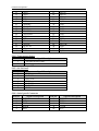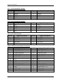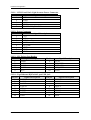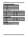
1
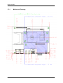
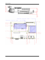
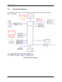
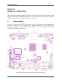
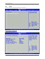
PEB-2739I Series
Embedded System Board
User's Manual
Version 1.0
Copyright © Portwell, Inc., 2010. All rights reserved.
All other brand names are registered trademarks of their respective owners.
Table of Contents
How to Use This Manual
Chapter 1 System Overview.......................................................................................................1-1
1.1 Introduction ....................................................................................................... 1-1
1.2 Check List........................................................................................................... 1-2
1.3 Product Specification........................................................................................ 1-2
1.3.1 Mechanical Drawing................................................................................ 1-5
1.4 System Architecture.......................................................................................... 1-7
Chapter 2 Hardware Configuration ...........................................................................................2-1
2.1 Jumper Setting ................................................................................................... 2-1
2.2 Connector Allocation........................................................................................ 2-2
Chapter 3 System Installation....................................................................................................3-1
3.1 System Architecture.......................................................................................... 3-1
3.2 System Architecture.......................................................................................... 3-1
3.3 System Architecture.......................................................................................... 3-2
3.3.1 Mechanical Drawing................................................................................ 3-2
3.3.2 Intel Integrated Graphics GMCH Chip ................................................ 3-2
3.3.3 Intel Gigabit Ethernet Controller ........................................................... 3-2
3.3.4 Audio Controller ...................................................................................... 3-3
3.4 Clear CMOS Operation .................................................................................... 3-3
3.5 WDT Function ................................................................................................... 3-3
3.6 GPIO.................................................................................................................... 3-4
3.7 WDT/GPIO Assembly Code........................................................................... 3-4
Chapter 4 BIOS Setup Information............................................................................................4-1
4.1 Entering Setup -- Launch System Setup ........................................................ 4-1
4.2 Main .................................................................................................................... 4-2
4.3 Advanced ........................................................................................................... 4-3
4.4 PCIPnP.............................................................................................................. 4-15
4.5 Boot ................................................................................................................... 4-17
4.6 Security ............................................................................................................. 4-22
4.7 Chipset.............................................................................................................. 4-23
4.8 Exit..................................................................................................................... 4-27
Chapter 5 Troubleshooting ........................................................................................................5-1
5.1 Hardware Quick Installation........................................................................... 5-1
5.2 BIOS Setting ....................................................................................................... 5-1
Appendix A System Memory Address Map
Appendix B Interrupt Request Lines (IRQ)
Preface
How to Use This Manual
The manual describes how to configure your PEB-2739I to meet various operating
requirements. It is divided into five chapters, with each chapter addressing a basic
concept and operation of Single Board Computer.
Chapter 1 : System Overview. Presents what you have in the box and give you an
overview of the product specifications and basic computer architecture.
Chapter 2 : Hardware Configuration. Shows the definitions and locations of
Jumpers and Connectors that you can easily configure your embedded board.
Chapter 3 : System Installation. Describes how to properly mount the CPU, main
memory and Compact Flash to get a safe installation and provides a programming
guide of Watch Dog Timer function.
Chapter 4 : BIOS Setup Information. Specifies the meaning of each setup
parameters, how to get advanced BIOS performance and update new BIOS. In
addition, POST checkpoint list will give users some guidelines of trouble-shooting.
Chapter 5 : Troubleshooting. Provides various useful tips to quickly get PEB-2739I
running with success. As basic hardware installation has been addressed in Chapter
3, this chapter will basically focus on system integration issues, in terms of backplane
setup, BIOS setting, and OS diagnostics.
The content of this manual is subject to change without prior notice. These changes
will be incorporated in new editions of the document. Portwell may make
supplement or change in the products described in this document at any time.
Updates to this manual, technical clarification, and answers to frequently asked
questions will be shown on the following web site: http://www.portwell.com.tw/.
System Overview
Chapter 1
System Overview
1.1
Introduction
Portwell Inc., a world-leading innovator in the Industrial PC (IPC) market and a
member of the Intel® Embedded and Communications Alliance (Intel ECA),
announced today the Portwell PEB-2739I utilizing the Intel® ECX form factor based
on the Intel® Atom™ processor Z500PT series and the Intel® System Controller Hub
US15WPT. The new micro-architecture of the Intel® platform will provide a range of
low power, wide temperature and fanless devices such as Panel PC, Kiosk, DS,
Medical, Military, Government and Industrial automation and control applications.
PEB-2739I is specifically designed to operate at a very low power consumption of
less than 10 watts at full loading. It supports dual independent display by LVDS and
SDVO daughter card (DVI/VGA/LVDS, by request).
Based on the Intel® Atom™ processor Z500PT series platform, the PEB-2739I takes
advantage of the processor’s very low power consumption, Ground-breaking power
management techniques and wide temperature so it can be a truly industrial
temperature and fanless configuration. In addition, the PEB-2739I supports DC 12V
input, one SO-DIMM memory slot for DDR2 SDRAM up to 2GB, and comes with
one SATA, one CompactFlash® socket, one SDVO connector (with one PCIE x1 and
USB signal), one gigabit Ethernet, two RS232, six USB2.0 and one SDIO connector.
PEB-2739I features:
z
Intel® Atom™ processor Z500PT series and System Controller Hub US15WPT
z
One 200-pin SO-DIMM support DDR2 SDRAM up to 2GB
z
Dual independent display: SDVO(by VGA/DVI/LVDS daughter card) and
24bit LVDS
z
One Gigabit Ethernet
z
TPM (Trusted Platform Module) could be added on board (optional)
z
Customization (Extension card): BTB connector with SDVO/USB/PCI-E x1
signal and SDIO pin header
z
Storage: One SATA / One CompactFlash / One USB Flash / One SDIO
z
12V DC input
PEB-2739I User’s Manual
1-1
System Overview
1.2
Check List
The PEB-2739I package should include the following items:
z
z
z
z
One PEB-2739I embedded system board
One 2-in-1 Heatsink
One SATA Cable
One Installation Resources CD Title
If any of these items is damaged or missing, please contact your vendor and keep all
packing materials for future replacement and maintain.
1.3
z
z
z
z
z
z
z
z
z
z
z
z
Product Specification
CPU
On board Intel® Atom™ Z510PT (1.1GHz) / Z520PT (1.33GHz) processor
CPU clock bus: Z520PT: 533MHz / Z510PT:400MHz
Chipset
Intel® System Controller Hub US15WPT
System BIOS
AMI BIOS
Main Memory
One 200-pin DDR2 SODIMM socket supports up to 2GB dual channel
400/533MHz memory
Serial Port
Support one RS-232 and one RS-232/422/485 selectable
USB Interface
Support six USB (Universal Serial Bus) ports, four on rear I/O and two on
board header for internal devices. USB port6, 7 can support USB 2.0 only base
on Intel specification.
Client USB
Support one Client USB on board edge
Audio Interface
Connector for Mic-In and Line-Out
Keyboard and PS/2 Mouse interface
Support one PS/2 header for keyboard and mouse
Watch Dog Timer
Support WDT function through software programming for enable/disable and
interval setting
General system reset
On Board VGA
Intel® System Controller Hub US15WPT integrated GMA 500 Graphic device
On-board Ethernet
One Gigabit Ethernet (10/100/1000 Mbits/sec) LAN ports using Intel PCIExpressx1interface GbE Ethernet Controller (82574IT)
PEB-2739I User’s Manual
1-2
System Overview
z
z
z
On Board I/O
- Rear I/O
‧Line-Out
‧MIC-In
‧Four USB ports
‧One DB-9 support RS-232/422/485
‧Fast Ethernet port (RJ45)
‧12V DC Jack
- Internal I/O
‧One SATA connector(with Power)
‧One Type II CompactFlash socket
‧One LVDS port
‧One SDVO port (BTB connector with SDVO/USB/PCI-E x1 signal)
‧One SDIO port (2x8-pin, 2mm-pitch box header)
‧One RS-232 port (2x5-pin, 2mm-pitch box header)
‧Two USB 2.0 ports (2x5-pin, 2mm-pitch header)
‧One Client USB connector
‧One 3-pin power connector for system fan
‧One power output port
‧Power on/off LED, Hard drive activity LED and system Reset switch
headers
‧On-board programmable 8-bit Digital I/O interface
System Monitoring Feature
Monitor system temperature and major power sources.
Outline Dimension (L X W):
146mm X 105mm
PEB-2739I User’s Manual
1-3
System Overview
z Power requirements
System Configuration
CPU Type
SBC BIOS
Memory
Intel® Atom™ CPU [email protected] FSB:400MHz
Portwell,Inc.PEB-2739I BIOS Rev.:R1.00.E2(09232009)
VGA Card
VGA Driver
LAN Card
LAN Driver
Audio Card
Audio Driver
Chip Driver
USB 2.0 Driver
IDE HDD
Compact Flash
USB-CDROM
Power Supply
Onboard Intel Corporation US15WPT Embedded Graphics Chipset Function
L2:512K
Transcend DDR2-533 1GB(SamSung K4T51083QE)
Intel Corporation US15WPT Embedded Graphics Chipset Ver:10.1.0.1390
Onboard Intel 82574IT Gigabit Chipset
Intel® 82574IT Gigabit Network Connection Ver:10.6.15.0
Onboard Realtek ALC662 Audio Chipset
Realtek High Definition Audio Ver:6.0.1.5680
Intel® Chipset Device Software Ver:8.8.0.1011
Intel® SCH Family USB2 Enhanced Host Controller Ver:8.8.0.1001
WD WD1200BEVE 120GB 2.5”
Transcend Ultra DMA 1GB(TS1GCF45IF-A5)
ASUS CB-52164 DVD-ROM
Seasonic SSA-0651-1
Programs for loading both CPU & VGA: Run Burning Test V5.3
RUN time: 10 / 30 Minutes.
Full Loading
Full Loading
Item
Power ON
10Min
30Min
DC 12V
USB Loading Test
z
z
z
0.6A
0.88A
4.73 V/ 510 mA
0.89A
Operating Temperature:
-40°C ~ 80°C
Storage Temperature:
-40°C ~ 80°C
Relative Humidity:
5% ~ 90%, non-condensing
PEB-2739I User’s Manual
1-4
System Overview
1.3.1
Mechanical Drawing
PEB-2739I User’s Manual
1-5
System Overview
PEB-2739I User’s Manual
1-6
System Overview
1.4
System Architecture
All of details operating relations are shown in PEB-2739I System Block Diagram.
PEB-2739I Block Diagram
PEB-2739I User’s Manual
1-7
Hardware Configuration
Chapter 2
Hardware Configuration
This chapter gives the definitions and shows the positions of jumpers, headers and
connector. All of the configuration jumpers on PEB-2739I are in the proper position.
The default settings are indicated with a star sign (Ì).
2.1
Jumper Setting
For users to customize PEB-2739I’s features. In the following sections, Short means
covering a jumper cap over jumper pins; Open or N/C (Not Connected) means
removing a jumper cap from jumper pins. Users can refer to Figure 2-1 for the
Jumper and Connector locations.
PEB-2739I Jumper and Connector Locations (Top)
PEB-2739I User’s Manual
2-1
Hardware Configuration
JP1 : Clear CMOS
JP1
Open
Short
Function
Normal operation Ì
Clear CMOS
JP2 : 5V / 3.3V Panel power selection
JP2
1-2 Short
2-3 Short
Function
3.3V
5V Ì
JP3 : Microcontroller programming
JP3
1-2, 3-4, 5-6 Short
1-2, 3-4, 5-6 Open
Function
Normal operation Ì
Programming microcontroller
JP4 : 5V / 3.3V backlight enable pin power level selection
JP4
1-2 Short
2-3 Short
Function
3.3V
5V Ì
JP5 : Serial port 2 function selection
JP5
5-6, 9-11, 10-12, 15-17, 16-18 Short
3-4, 7-9, 8-10, 13-15, 14-16, 21-22 Short
1-2, 7-9, 8-10, 19-20 Short
2.2
Function
RS-232 Ì
RS-422
RS-485
Connector Allocation
I/O peripheral devices are connected to the interface connectors.
Connector Function List
Connector
CN1
CN2
CN3
CN4
CN5
CN6
CN7
CN8
CN9
CN10
CN11
Function
Remark
SATA port 1
SDIO Port (Support SD 1.1 and MMC 4.0 only)
PATA 44-Pin (IDE)
Temperature Sense
SATA port 2
Serial port 2
USB port 6,7
USB port 0,2
8 bit GPIO
Single channel LVDS panel interface
Panel backlight inverter’s power
PEB-2739I User’s Manual
2-2
Hardware Configuration
CN12
CN13
CN14
CN15
CN16
CN17
CN18
CN19
CN20
CN21
CN22
CN23
ATX power source
LPC Debug Port
Giga Ethernet with USB port 1,3
Microcontroller programmer
PS/2 Keyboard & Mouse
USB port 4,5
Audio port (Stereo line output, microphone input)
CRT with serial port 1
Front Panel
FAN
DDR2 SO-DIMM 200Pin
Compact flash
Pin Assignments of Connectors
CN1 : SATA Port 1
Pin No.
1
2
3
4
5
6
7
Signal Description
GND
SATATX+
SATATXGND
SATARX+
SATARXGND
CN2 : SDIO Connector
Pin No.
1
3
5
7
9
11
13
15
Signal Description
SDIO_DATA0
SDIO_DATA1
SDIO_DATA2
SDIO_DATA3
SDIO_DATA4
SDIO_DATA5
SDIO_DATA6
SDIO_DATA7
Pin No.
2
4
6
8
10
12
14
16
Signal Description
+3.3V
SDIO_CLK
SDIO_CMD
+3.3V
GND
SDIO_CD#
SDIO_WP
GND
Pin No.
2
4
6
8
10
Signal Description
GND
PDD8
PDD9
PDD10
PDD11
CN3 : Hard Disk 44-pin Connector
Pin No.
1
3
5
7
9
Signal Description
R_PLT_RST#
PDD7
PDD6
PDD5
PDD4
PEB-2739I User’s Manual
2-3
Hardware Configuration
11
13
15
17
19
21
23
25
27
29
31
33
35
37
39
41
43
PDD3
PDD2
PDD1
PDD0
GND
PDDREQ
PDIOW#
PDIOR#
PDIORDY
PDDACK#
IRQ14#
PDA1
PDA0
PDCS1#
IDEACT#
+5V
GND
12
14
16
18
20
22
24
26
28
30
32
34
36
38
40
42
44
PDD12
PDD13
PDD14
PDD15
N/C
GND
GND
GND
GND
GND
N/C
GND
PDA2
PDCS3#
GND
+5V
N/C
CN4 : Temperature Sense
Pin No.
1
2
Signal Description
Thermal resister 10K+
Analog ground
CN5 : SATA Port 2
Pin No.
1
2
3
4
5
6
7
Signal Description
GND
SATATX+
SATATXGND
SATARX+
SATARXGND
CN6 : Serial port 2 Connector
Pin No.
1
3
5
7
9
Signal Description
DCD1#
TXD1#
GND
RTS1#
RI1#
PEB-2739I User’s Manual
Pin No.
2
4
6
8
10
Signal Description
RXD1#
DTR1#
DSR1#
CTS1#
N/C
2-4
Hardware Configuration
CN7 : USB Port6&Port7 Header
Pin No.
1
3
5
7
9
Signal Description
+5V
USBD6USBD6+
GND
N/C
Pin No.
2
4
6
8
Signal Description
+5V
USBD7USBD7+
GND
CN8 : USB Port0&Port2 Header
Pin No.
1
3
5
7
9
Signal Description
+5V
USBD0USBD0+
GND
N/C
Pin No.
2
4
6
8
Signal Description
+5V
USBD2USBD2+
GND
Pin No.
2
4
6
8
10
Signal Description
LPC_GP14
LPC_GP15
LPC_GP16
LPC_GP17
+5V
Pin No.
2
4
6
8
10
12
14
16
18
20
22
24
26
28
30
Signal Description
LVDSA_DATA0LVDSA_DATA1LVDSA_DATA2LVDSA_DATA3LVDSA_CLKN/C
N/C
N/C
N/C
N/C
LVDS_I2C_CLK
BACKLIGHT_CTL
GND
VDD_LVDS
VDD_LVDS
CN9 : 8 bit GPIO Header
Pin No.
1
3
5
7
9
Signal Description
LPC_GP10
LPC_GP11
LPC_GP12
LPC_GP13
GND
CN10 : LVDS Panel Interface Connector
Pin No.
1
3
5
7
9
11
13
15
17
19
21
23
25
27
29
Signal Description
LVDSA_DATA0+
LVDSA_DATA1+
LVDSA_DATA2+
LVDSA_DATA3+
LVDSA_CLK+
N/C
N/C
N/C
N/C
N/C
LVDS_I2C_DATA
GND
GND
VDD_LVDS
N/C
PEB-2739I User’s Manual
2-5
Hardware Configuration
CN11 : LVDS Panel Back Light Inverter Power Connector
Pin No.
1
2
3
4
5
Signal Description
+5V
GND
+12V
GND
BACKLIGH_ENABLE
CN12 : Power Connector
Pin No.
1
2
3
4
5
6
7
8
Signal Description
+5V
+5V
+5V Standby
+12V
PS_ON#
GND
GND
GND
CN13 : LPC Debug Port Header
Pin No.
1
3
5
7
9
Signal Description
LAD0
LAD1
LAD2
LAD3
N/C
Pin No.
2
4
6
8
10
Signal Description
+3.3V
PLT_RST#
LFRAME#
LPC_PCID
GND
CN14 : Giga Ethernet RJ45 with 2 port USB Jack
Pin No.
1
3
5
7
9
11
13
15
Signal Description
LAN 0+
LAN 1+
LAN 2LAN 3+
+5V
USBD1USBD1+
GND
PEB-2739I User’s Manual
Pin No.
2
4
6
8
10
12
14
16
Signal Description
LAN 0LAN 2+
LAN 1LAN 3+5V
USBD3USBD3+
GND
2-6
Hardware Configuration
CN15 : Microcontroller programmer Header
Pin No.
1
2
3
4
5
6
Signal Description
Vpp
+3.3V
GND
I2C_DATA
I2C_CLK
N/C
CN16 : PS/2 Keyboard/Mouse
Pin No.
B1
B2
B3
B4
B5
B6
Signal Description
KB_DATA
N/C
GND
+5V
KB_CLK
N/C
Pin No.
T1
T2
T3
T4
T5
T6
Signal Description
MS_DATA
N/C
GND
+5V
MS_CLK
N/C
Pin No.
B1
B2
B3
B4
Signal Description
CN17 : USB Port4&Port5 Jack
Pin No.
T1
T2
T3
T4
Signal Description
+5V
USBD5USBD5+
GND
+5V
USBD4USBD4+
GND
CN18 : Audio Jack
Pin No.
Top
Bottom
Signal Description
Stereo line out
Microphone input
PEB-2739I User’s Manual
2-7
Hardware Configuration
CN19 : CRT with Serial port 1 Connector (DB15+DB9)
Pin No.
B1
B3
B5
B7
B9
B11
B13
B15
T1
T3
T5
T7
T9
Signal Description
RED
BLUE
GND
GND
N/C
MONOPU
HSYNC
RED
DCD2#
TXD2#
GND
RTS2#
RI2#
Pin No.
B2
B4
B6
B8
B10
B12
B14
T2
T4
T6
T8
Signal Description
GREEN
MON2PU
GND
GND
GND
5VDDCDA
VSYNC
RXD2#
DTR2#
DSR2#
CTS2#
CN20 : Front Panel Header
Pin No.
1
3
5
7
Signal Description
SUS_LED
HDD_LED
GND
PWR_ON_SW#
Pin No.
2
4
6
8
Signal Description
5V_Dual
+3.3V
RESET
GND
CN21 : Fan Connector
Pin No.
1
2
3
Signal Description
GND
+12V
RPM
CN22 : DDR2 SO-DIMM 200Pin Connector
CN23 : Compact Flash connector
Pin No.
1
2
3
4
5
6
7
8
9
Signal Description
Ground
Data 3
Data 4
Data 5
Data 6
Data 7
HDC CS0#
Ground
Ground
PEB-2739I User’s Manual
Pin No.
26
27
28
29
30
31
32
33
34
Signal Description
N/C
Data 11
Data 12
Data 13
Data 14
Data 15
HDC CS1#
N/C
IOR#
2-8
Hardware Configuration
10
11
Ground
Ground
35
36
12
13
14
15
16
17
18
19
20
21
22
23
24
25
Ground
+5V
Ground
Ground
Ground
Ground
HDC SDA2
HDC SDA1
HDC SDA0
Data 0
Data 1
Data 2
N/C
N/C
37
38
39
40
41
42
43
44
45
46
47
48
49
50
PEB-2739I User’s Manual
IOW#
Write Enable(pull-high 4.7k to
5V)
IRQ
+5V
CSEL (pull-low 470 to Gnd)
N/C
RESET#
IORDY
DREQ#
DACK#
HDC ACT#
PDIAG# (Pull-Low 150 ohms)
Data 8
Data 9
Data 10
Ground
2-9
System Installation
Chapter 3
System Installation
This chapter provides you with instructions to set up your system. The additional
information is enclosed to help you set up onboard PCI device and handle Watch
Dog Timer (WDT) and operation of GPIO in software programming.
3.1
System Architecture
- Intel® Atom™ Processor Z510PT (512K Cache, 1.10 GHz, 400 MHz FSB)
- Intel® Atom™ Processor Z520PT (512K Cache, 1.33 GHz, 533 MHz FSB)
3.2
System Architecture
PEB-2739I provide 1 x 200pin SO-DIMM sockets which supports 400/533 DDR2SODIMM as main memory, Non-ECC (Error Checking and Correcting), non-register
functions. The maximum memory can be up to 2GB. Memory clock and related
settings can be detected by BIOS via SPD interface.
For system compatibility and stability, do not use memory module without brand.
Memory configuration can be set to either one double-sided DIMM in one DIMM
socket.
Beware of the connection and lock integrity from memory module to socket.
Inserting improperly it will affect the system reliability.
Before locking, make sure that all modules have been fully inserted into the card
slots.
Note:
To insure the system stability, please do not change any of DRAM parameters in
BIOS setup to modify system the performance without acquired technical
information.
PEB-2739I User’s Manual
3-1
System Installation
3.3
System Architecture
To install your PEB-2739I into standard chassis or proprietary environment, please
perform the following:
Step 1 : Check all jumpers setting on proper position
Step 2 : Install and configure CPU and memory module on right position
Step 3 : Place PEB-2739I into the dedicated position in the system
Step 4 : Attach cables to existing peripheral devices and secure it
WARNING
Please ensure that SBC is properly inserted and fixed by mechanism.
Note:
Please refer to section 3.3.1 to 3.3.7 to install INF/VGA/LAN/Audio drivers.
3.3.1
Mechanical Drawing
PEB-2739I uses state-of-art Intel® Z510 CPU. It’s a new chipset that some old
operating systems might not be able to recognize. To overcome this compatibility
issue, for Windows Operating Systems such as Windows XP/Vista/Win7, please
install its INF before any of other Drivers are installed. You can find very easily this
chipset component driver in PEB-2739I CD-title.
3.3.2
Intel Integrated Graphics GMCH Chip
PEB-2739I uses Intel GMA500 integrated graphic chipset to gain an outstanding
graphic performance. Shared 8 accompany it to 128MB system DDR2-SODIMM with
Total Graphics Memory. PEB-2739I supports VGA, LVDS dual display. This
combination makes PEB-2739I an excellent piece of multimedia hardware.
With no additional video adaptor, this onboard video will usually be the system
display output. By adjusting the BIOS setting to disable on-board VGA, an add-on
PCI-Express by 1 VGA card can take over the system display.
Drivers Support
Please find all the drivers in the PEB-2739I CD-title. Drivers support , Windows
XP/Vista/Win7.
3.3.3
Intel Gigabit Ethernet Controller
Drivers Support
Please find INTEL 82574IT LAN driver in /Ethernet directory of PEB-2739I CD-title.
The drivers support Windows XP/Vista/Win7.
PEB-2739I User’s Manual
3-2
System Installation
3.3.4
Audio Controller
Please find Intel® High Definition Audio driver form PEB-2739I CD-title. The
drivers support Windows XP/Vista/Win7.
3.4
Clear CMOS Operation
The following table indicates how to enable/disable Clear CMOS Function hardware
circuit by putting jumpers at proper position.
(JP7)RTC Reset
JP7
Function
1-2 Short
Normal operation *
1-2 Open
Clear CMOS
3.5
JP7
1-2 Short
1-2 Open
WDT Function
The algorithm of the WDT function can be simply described as a timer counting
process with an output event. The Time-Out period ( Twd ) can be set by software
commands or hardware jumpers that depend on the board circuit design and may be
different among the boards. This timer can be used to monitor a software hang.
PEB-2739I allows users to control WDT by issuing dynamic software commands.The
WDT starts counting when it is activated. It will cause a system reset once it expires.
Before WDT expires, a refreshing command with a Twd can be issued to re-count
WDT and continue the status monitoring. If the system encounters a software or
application hang, WDT will generate a system reset after its timeout.
The related Control Registers of WDT are included in the following programming
guide that is written in C language. User can write a non-zero value ( defined as
Twd ) into the Time-out Value Register ( CR_Twd ) to enable WDT. Users can write
0x00 and then Twd to CR_Twd to refresh WDT. To refresh WDT, the time tolerance
of refreshing interval must be considered. The smaller of Twd, the more deviation of
WDT and you need to include more tolerance. “Let Twd be longer than 2 seconds” is
the recommendation due to the limitation of Winbond W83627DHG WDT. You can
call Portwell support center for reference. The value read back from CR_Twd
indicates the counting down value instead of the original Twd. System will be reset
after the Time-out Value to be counted down to zero. Users can directly fill a zero
value into CR_Twd to disable WDT immediately. To ensure a successful access to
the desired Control Register, the following programming guide should be followed.
Programming guide :
PEB-2739I User’s Manual
3-3
System Installation
3.6
GPIO
The PEB-2739I provides 8 programmable input or output ports that can be
individually configured to perform a simple basic I/O function. Users can configure
each individual port to become an input or output port by programming register bit
of I/O Selection. To invert port value, the setting of Inversion Register has to be
made. Port values can be set to read or write through Data Register.
The GPIO ports are located on J9 shown as follows.
Notes : Do not short-circuit Pin 9 and 10 of J9!
3.7
WDT/GPIO Assembly Code
#include <stdio.h>
#include <stdlib.h>
#include <conio.h>
void WDT_Enable(int time,int mode);
void WDT_Disable();
void GPIO_Set_Mode(int bit,int mode);
void GPIO_Write(int bit,int data);
int GPIO_Read(int bit);
void main(){
outp (0x2e,0x87);//Input SIO entry key
outp (0x2e,0x87);
//WDT sample code
WDT_Enable(20,0);
//WDT_Disable();
//GPIO sampe code
GPIO_Set_Mode(0,0);//set GPIO 30 for output
GPIO_Set_Mode(1,1);//set GPIO 31 for input
GPIO_Set_Mode(2,1);//Set GPIO 32 for input
GPIO_Write(0,1);//Set GPIO 30 for high
outp (0x2e,0xAA);//Input SIO Exit key
return;
}
// time<255
, mode 0 =sec, 1 =min
void WDT_Enable(int time,int mode){
outp (0x2e,0x2d);
PEB-2739I User’s Manual
3-4
System Installation
outp (0x2f,inp(0x2f)&0xfe);//Enable WDT function
outp (0x2e,0x07);
outp (0x2f,0x08); //entry device 8
outp (0x2e,0xF5);
outp (0x2f,inp(0x2f)|(mode*0x08)); //bit3 0:second,1 Minute
outp (0x2e,0xf6);
outp (0x2f,time);// Set time (sec/min)
outp (0x2e,0xf7);
outp (0x2f,inp(0x2f)|0xc0);//enable reset time by mouse/keyboard
interrupt
}
void WDT_Disable(){
outp (0x2e,0x2d);
outp (0x2f,inp(0x2f)|0x01);//Disable WDT function
}
//bit 0~7=GPIO 30~37, mode 0=output 1=input
void GPIO_Set_Mode(int bit,int mode){
int tmp=1<<bit;
outp (0x2e,0x07);
outp (0x2f,0x09);// entry device 9
outp (0x2e,0xf0);
outp (0x2f,(inp(0x2f)&~tmp)|(tmp*mode));//0 for output,1 for intput
}
//data 0 for low, 1 for high
void GPIO_Write(int bit,int data){
int tmp=1<<bit;
outp (0x2e,0x07);
outp (0x2f,0x09);// entry device 9
outp (0x2e,0xf1);
outp (0x2f,(inp(0x2f)&~tmp)|(tmp*data));//0 for low,1 for high
}
//high return 1, low return 0
int GPIO_Read(int bit){
int tmp=1<<bit;
int data;
outp (0x2e,0x07);
PEB-2739I User’s Manual
3-5
System Installation
outp (0x2f,0x09);// entry device 9
outp (0x2e,0xf1);
data=inp(0x2f)&~tmp;//read bit
if (data==0)
return 0;
else
return 1;
PEB-2739I User’s Manual
3-6
BIOS Setup Information
Chapter 4
BIOS Setup Information
PEB-2739I is equipped with the AMI BIOS stored in Flash ROM. These BIOS has a
built-in Setup program that allows users to modify the basic system configuration
easily. This type of information is stored in CMOS RAM so that it is retained during
power-off periods. When system is turned on, PEB-2739I communicates with
peripheral devices and checks its hardware resources against the configuration
information stored in the CMOS memory. If any error is detected, or the CMOS
parameters need to be initially defined, the diagnostic program will prompt the user
to enter the SETUP program. Some errors are significant enough to abort the start
up.
4.1
Entering Setup -- Launch System Setup
Power on the computer and the system will start POST (Power On Self Test) process.
When the message below appears on the screen, press <Del> key to enter Setup.
Press <Del> to enter SETUP
If the message disappears before you respond and you still wish to enter Setup,
restart the system by turning it OFF and On or pressing the RESET button. You may
also restart the system by simultaneously pressing <Ctrl>, <Alt>, and <Delete> keys.
Press <F1> to Run SETUP or Resume
The BIOS setup program provides a General Help screen. You can call up this screen
from any menu by simply pressing <F1>. The Help screen lists the appropriate keys
to use and the possible selections for the highlighted item. Press <Esc> to exit the
Help screen.
PEB-2739I User’s Manual
4-1
BIOS Setup Information
4.2
Main
Use this menu for basic system configurations, such as time, date etc.
AMI BIOS, Processor, System Memory
These items show the firmware and hardware specifications of your system. Read
only.
System Time
The time format is <Hour> <Minute> <Second>. Use [+] or [-] to configure system
Time.
System Date
The date format is <Day>, <Month> <Date> <Year>. Use [+] or [-] to configure
system Date.
PEB-2739I User’s Manual
4-2
BIOS Setup Information
4.3
Advanced
Use this menu to set up the items of special enhanced features.
PEB-2739I User’s Manual
4-3
BIOS Setup Information
CPU Configuration
These items show the advanced specifications of your CPU. Read only.
Hardware Prefetcher
The choice: Disabled, Enabled.
Adjacent Cache Line Prefetch
The choice: Disabled, Enabled.
Max CPUID Value Limit
Disabled for Windows XP
The choice: Disabled, Enabled.
Execute-Disable Bit capability
When disabled, force the XD feature flag to always return 0
The choice: Disabled, Enabled.
PEB-2739I User’s Manual
4-4
BIOS Setup Information
Hyper Threading Technology
“Enabled” for Windows XP and Linux 2.4.X (OS optimized for Hyper-Threading
Technology and “Disabled” for other OS (OS not optimized for Hyper-Threading
Technology).
The choice: Enabled, Disabled.
Intel(R) Speed Step (tm) Tech
Disable: Disable GV3.
Enable: Enable GV3.
IDE Configuration
The IDE Configuration the IDE devices, such as hard disk drive or CD-ROM drive. It
uses a separate sub menu to configure each hard disk drive (Master and Slave).
ATA/IDE Configuration
The choice: Disabled, Compatible, Enabled.
PEB-2739I User’s Manual
4-5
BIOS Setup Information
Primary IDE Master / Slave
While entering setup, BIOS auto detects the presence of IDE devices. This displays
the status of auto detection of IDE devices.
[Type] Press PgUp/<+> or PgDn/<-> to select [Manual], [None] or [Auto] type.
You can use [Manual] to define your own drive type manually.
[LBA/Large Mode] Enabling LBA causes Logical Block Addressing to be used in
place of Cylinders, Heads and Sectors.
[Block (Multi-Sector Transfer)] Any selection except Disabled determines the
number of sectors transferred per block.
[PIO Mode] Indicates the type of PIO (Programmed Input/Output)
[DMA Mode] Indicates the type of Ultra DMA
[S.M.A.R.T.] This allows you to activate the S.M.A.R.T. (Self-Monitoring Analysis &
Reporting Technology) capability for the hard disks. S. M.A.R.T is a utility that
monitors your disk status to predict hard disk failure. This gives you an opportunity
to move data from a hard disk that is going to fail to a safe place before the hard disk
becomes offline.
[32 Bit Data Transfer] Enable/Disable 32-bit Data Transfer.
PEB-2739I User’s Manual
4-6
BIOS Setup Information
Hard Disk Write Protect
Disabled/Enabled device write protection, this will be effective only if device is
accessed through BIOS.
The choice: Disabled, Enabled.
IDE Detect Time Out (Sec)
Select the time out value for detecting ATA/ATAPI device (s).
The choice: 0, 5, 10, 15, 20, 25, 30, 35.
ATA(PI) 80Pin Cable Detection
Select the mechanism for detecting 80Pin ATA (PI) cable.
The choice: Host & Device, Host, Device.
Super IO Configuration
Serial Port 1 Address/IRQ
Allows BIOS Select Serial Port1 Base Addresses.
The choice: Address: Disabled, 3F8, 3E8, 2E8,
IRQ: 3, 4, 10, 11.
PEB-2739I User’s Manual
4-7
BIOS Setup Information
Serial Port 2 Address/IRQ
Allows BIOS Select Serial Port2 Base Addresses.
The choice: Address: Disabled, 2F8, 3E8, 2E8,
IRQ: 3, 4, 10, 11.
Serial Port 2 Mode
The choice: Normal, IrDA, ASK IR,
Watch Dog Timer Set
This BIOS testing option is able to reset the system according to the selected table.
The Choice: Disabled, 10, 20, 30, 40 sec. 1, 2, 4 min.
Hardware Health Configuration
Configuration / monitor the Hardware Health.
PEB-2739I User’s Manual
4-8
BIOS Setup Information
ACPI Settings
Select for Advanced ACPI Configuration.
General ACPI Configuration
PEB-2739I User’s Manual
4-9
BIOS Setup Information
Suspend mode
This item specifies the power saving modes for ACPI function. If your operating
system supports ACPI, you can choose to enter the Standby mode in S1 (POS) or S3
(STR) fashion through the setting of this field. Options are:
[S1 (POS)] The S1 sleep mode is a low power state. In this state, no system context is
lost (CPU or chipset) and hardware maintains all system contexts.
[S3 (STR)] The S3 sleep mode is a lower power state where the information of system
configuration and open applications/ files is saved to main memory that remains
powered while most other hardware components turn off to save energy. The
information stored in memory will be used to restore the system when a “wake up”
event occurs.
Advanced ACPI Configuration
Advanced ACPI Configuration settings, Use this section to configure additional
ACPI options.
ACPI Version Features
Enable RSDP pointers to 64-bit Fixed System Description Tables.
The choice: ACPI v1.0 / ACPI v2.0 / ACPI v3.0.
PEB-2739I User’s Manual
4-10
BIOS Setup Information
ACPI APIC support
Include ACPI APIC table pointer to RSDT pointer list.
The choice: Disabled, Enabled.
AMI OEMB table
Include OEMB table pointer to R(X) SDT pointer list.
The choice: Disabled, Enabled.
Headless mode
Enable / Disable Headless operation mode through ACPI.
The choice: Disabled, Enabled.
South Bridge ACPI Configuration
The South Bridge ACPI related Configuration settings, Use this section to configure
additional ACPI options.
PEB-2739I User’s Manual
4-11
BIOS Setup Information
APIC ACPI SCI IRQ
Enable / Disable APIC ACPI SCI IRQ.
The choice: Disabled, Enabled.
USB Device Wakeup From S3/S4
Enable / Disable USB device Wake from S3/S4 mode.
The choice: Disabled, Enabled.
MPS Configuration
Configure the Multi-Processor Table.
MPS Revision
This field allows you to select which MPS (Multi-Processor Specification) version to
be used for the operating system. You need to select the MPS version supported by
your operating system. To find out which version to use, consult the vendor of your
operating system.
The choice: 1.1, 1.4.
PEB-2739I User’s Manual
4-12
BIOS Setup Information
Smbios Configuration
SMBIOS Configuration Menu
Smbios Smi Support
SMBIOS SMI Wrapper support for PnP Function 50h-54h
The choice: Disabled, Enabled.
PEB-2739I User’s Manual
4-13
BIOS Setup Information
USB Configuration
Legacy USB Support
Set to [Enabled] if you need to use any USB 1.1/2.0 device in the operating system
that does not support or have any USB 1.1/2.0 driver installed, such as DOS and
SCO Unix.
The choice: Disabled, Enabled, Auto.
USB 2.0 Controller Mode
This setting specifies the operation mode of the onboard USB 2.0 controller.
The choice: FullSpeed, HiSpeed.
BIOS EHCI Hand-Off
This is a workaround for OSes without EHCI hand-off support. The EHCI
ownership change should claim by EHCI driver.
The choice: Disabled, Enabled.
PEB-2739I User’s Manual
4-14
BIOS Setup Information
4.4
PCIPnP
Advanced PCI/PnP setting wrong values in below sections may cause system to
malfunction.
Clear NVRAM
Clear NVRAM during System Boot.
The choice: No, Yes.
Plug & Play O/S
No: lets the BIOS configure all the devices in the system.
Yes: lets the operating system configure Plug and Play (PnP) devices not required for
boot if your system has a Plug and Play operating system.
The choice: No, Yes.
PCI Latency Timer
Select value in units of PCI clocks for PCI device latency timer register.
The choice: 32, 64, 96, 128, 160, 192, 224, 248.
PEB-2739I User’s Manual
4-15
BIOS Setup Information
Allocate IRQ to PCI VGA
Yes: Assigns IRQ to PCI VGA card if card requests an IRQ.
No: Does not assign IRQ to PCI VGA card even if card requests an IRQ.
The choice: No, Yes.
Palette Snooping
Enabled: informs the PCI devices that an ISA graphics device is installed in the
system so the card will function correctly.
The choice: Disabled, Enabled.
PCI IDE BusMaster
Enabled: Uses PCI bus mastering for reading / writing to IDE drives.
The choice: Disabled, Enabled.
OffBoard PCI/ISA IDE Card
Some PCI IDE cards may require this to be set to the PCI slot number that is holding
the card. AUTO: Works for most PCI IDE cards
The choice: Auto, PCI Slot1, PCI Slot2, PCI Slot3, PCI Slot4, PCI Slot5, PCI Slot6.
IRQ 3 / IRQ 4 / IRQ5 / IRQ7 / IRQ 9 / IRQ 10 / IRQ 11 / IRQ 14 / IRQ 15
Available: Specified IRQ is available to be used by PCI/PnP devices.
Reserved: Specified IRQ is reserved for used by Legacy ISA devices.
The choice: Available, Reserved.
Reserved Memory Size
Select Size of memory block to reserve for legacy ISA devices.
The choice: Disabled, 16K, 32K, 64K.
PEB-2739I User’s Manual
4-16
BIOS Setup Information
4.5
Boot
Use this menu to specify the priority of boot devices.
Boot Settings Configuration
PEB-2739I User’s Manual
4-17
BIOS Setup Information
Quick Boot
Enabling this setting will cause the BIOS power-on self test routine to skip some of
its tests during boot up for faster system boot.
The choice: Disabled, Enabled.
Quiet Boot
This BIOS feature determines if the BIOS should hide the normal POST messages
with the motherboard or system manufacturer's full-screen logo. When it is enabled,
the BIOS will display the full-screen logo during the boot-up sequence, hiding
normal POST messages.
When it is disabled, the BIOS will display the normal POST messages, instead of the
full-screen logo.
Please note that enabling this BIOS feature often adds 2-3 seconds of delay to the
booting sequence. This delay ensures that the logo is displayed for a sufficient
amount of time. Therefore, it is recommended that you disable this BIOS feature for
a faster boot-up time.
The choice: Disabled, Enabled.
AddOn ROM Display Mode
This item is used to determine the display mode when an optional ROM is initialized
during POST. When set to [Force BIOS], the display mode used by AMI BIOS is
used. Select [Keep Current] if you want to use the display mode of optional ROM.
The choice: Force BIOS, Keep Current.
Bootup Num-Lock
This setting is to set the Num Lock status when the system is powered on.
Setting to [On] will turn on the Num Lock key when the system is powered on.
Setting to [Off] will allow users to use the arrow keys on the numeric keypad.
The choice: Off, On.
PS/2 Mouse support
Select [Enabled] if you need to use a PS/2-interfaced mouse in the operating system.
The choice: Disabled, Enabled, Auto.
PEB-2739I User’s Manual
4-18
BIOS Setup Information
Wait For ‘F1’ If Error
When this setting is set to [Enabled] and the boot sequence encounters an error, it
asks you to press F1. If disabled, the system continues to boot without waiting for
you to press any keys.
The choice: Disabled, Enabled.
Hit ‘DEL’ Message Display
Set this option to [Disabled] to prevent the message as follows:
Hit Del if you want to run setup
It will prevent the message from appearing on the first BIOS screen when the
computer boots. Set it to [Enabled] when you want to run the BIOS Setup Utility.
The choice: Disabled, Enabled.
Interrupt 19 Capture
Interrupt 19 is the software interrupt that handles the boot disk function. When
enabled, this BIOS feature allows the ROM BIOS of these host adaptors to "capture"
Interrupt 19 during the boot process so that drives attached to these adaptors can
function as bootable disks. In addition, it allows you to gain access to the host
adaptor's ROM setup utility, if one is available.
When disabled, the ROM BIOS of these host adaptors will not be able to "cap ture"
Interrupt 19. Therefore, you will not be able to boot operating systems from any
bootable disks attached to these host adaptors. Nor will you be able to gain access to
their ROM setup utilities.
The choice: Disabled, Enabled.
PEB-2739I User’s Manual
4-19
BIOS Setup Information
Boot Device Priority
1st Boot Device
The items allow you to set the sequence of boot devices where BIOS attempts to load
the disk operating system. First press <Enter> to enter the sub-menu. Then you may
use the arrow keys (↑↓) to select the desired device, then press <+>, <-> or
<PageUp>, <PageDown> key to move it up/down in the priority list.
The choice: (Network: IBA GE Slot 00C8 v1324), Disabled.
PEB-2739I User’s Manual
4-20
BIOS Setup Information
Hard Disk Drives
1st Drive
This setting allows users to set the priority of the removable devices. First press
<Enter> to enter the sub-menu. Then you may use the arrow keys (↑↓) to select the
desired device, then press <+>, <-> or <PageUp>, <PageDown> key to move it
up/down in the priority list.
PEB-2739I User’s Manual
4-21
BIOS Setup Information
4.6
Security
Use this menu to set supervisor and user passwords.
Supervisor Password / Change Supervisor Password
Supervisor Password controls access to the BIOS Setup utility. These settings allow
you to set or change the supervisor password.
User Password / Change User Password
User Password controls access to the system at boot. These settings allow you to set
or change the user password.
Boot Sector Virus Protection
Boot Sector Virus Protection.
The choice: Disabled, Enabled.
PEB-2739I User’s Manual
4-22
BIOS Setup Information
4.7
Chipset
This menu controls the advanced features of the onboard Northbridge and
Southbridge.
Onboard LAN PXE ROM Init
The choice: Disabled, Enabled.
PEB-2739I User’s Manual
4-23
BIOS Setup Information
North Bridge Chipset Configuration
Primary Graphic Adapter
Select which graphics controller to use as the primary boot device.
The choice: IGD, PCIe/IGD.
Internal Graphics Mode Select
Select the amount of system memory used by the internal graphics device.
The choice: Disable, Enabled, 1MB, Enabled, 4MB, Enabled, 8MB.
PEB-2739I User’s Manual
4-24
BIOS Setup Information
Video Function Configuration
Boot Display Device
The choice: Auto, Integrated LVDS, External CRT, External LVDS.
Local Flat Panel Scaling
The choice: Auto, Forced Scaling, Disabled.
Flat Panel Type
The choice: 640x480 (generic), 800x600 (generic), 1024x768 (generic), 1200x1024.
DPST Control
The choice: VBIOS Default, DPST Disabled, DPST Enabled at Level 1, DPST Enabled
at Level 2, DPST Enabled at Level 3, DPST Enabled at Level 4, DPST Enabled at
Level 5.
PEB-2739I User’s Manual
4-25
BIOS Setup Information
South Bridge Configuration
USB Functions
This setting specifies the function of the onboard USB controller.
The choice: Disabled, 2 USB Ports, 4 USB Ports, 6 USB Ports.
USB 2.0 Controller
Set to [Enabled] if you need to use any USB 2.0 device in the operating system that
does not support or have any USB 2.0 driver installed, such as DOS and SCO Unix.
The choice: Enabled, Disabled.
USB Client Controller
The choice: Enabled, Disabled.
SDIOController
The choice: Enabled, Disabled.
PEB-2739I User’s Manual
4-26
BIOS Setup Information
Audio Controller Codec
The choice: Auto, Azalia, Disabled.
SLP_S4# Min. Assertion Width
The choice: 4 to 5 seconds, 3 to 4 seconds, 2 to 3 seconds, 1 to 2 seconds.
Restore on AC Power Loss
This item allows user to configure the power status of using ATX power supply after
a serious power loss occurs.
The choice: Power Off, Power On, Last State.
Serial IRQ Mode
The choice: Continuous, Quiet.
PICE Port 0/1
The choice: Auto, Enabled, Disabled.
4.8
Exit
This menu allows you to load the BIOS default values or factory default settings into
the BIOS and exit the BIOS setup utility with or without changes.
PEB-2739I User’s Manual
4-27
BIOS Setup Information
Exit Saving Changes
Exit System Setup and save your changes to CMOS. Pressing <Enter> on this item
asks for confirmation: Save changes to CMOS and exit the Setup Utility.
Discard Changes and Exit
Abandon all changes and exit the Setup Utility.
Discard Changes
Abandon all changes and continue with the Setup Utility.
Load Optimal Defaults
Use this menu to load the default values set by the SBC manufacturer specifically for
optimal performance of the SBC.
Load Failsafe Defaults
Use this menu to load the default values set by the BIOS vendor for stable system
performance.
PEB-2739I User’s Manual
4-28
Troubleshooting
Chapter 5
Troubleshooting
This chapter provides a few useful tips to quickly get PEB-2739I running with
success. As basic hardware installation has been addressed in Chapter 2, this chapter
will primarily focus on system integration issues, in terms of BIOS setting, and OS
diagnostics.
5.1
Hardware Quick Installation
DC 12V Power Input
PEB-2739I supports DC12V input only(J21).
5.2
BIOS Setting
It is assumed that users have correctly adopted modules and connected all the
device
cables required before turning on ATX power. 200-pin DDR2 SO-DIMM, keyboard,
mouse, SATA hard disk, CF connector, VGA connector, device power cables, ATX
accessories are
good examples that deserve attention. With no assurance of properly and correctly
accommodating these modules and devices, it is very possible to encounter system
failures that result in malfunction of any device.
To make sure that you have a successful start with PEB-2739I, it is recommended,
when going with the boot-up sequence, to hit “DEL” key and enter the BIOS setup
menu to tune up a stable BIOS configuration so that you can wake up your system
far well.
PEB-2739I User’s Manual
5-1
Troubleshooting
Loading the default optimal setting
When prompted with the main setup menu, please scroll down to “Restore
Defaults”, press “Enter” and “Y” to load in default optimal BIOS setup. This will
force your BIOS setting back to the initial factory configuration. It is recommended
to do this so you can be sure the system is running with the BIOS setting that
Portwell has highly endorsed. As a matter of fact, users can load the default BIOS
setting any time when system appears to be unstable in boot up sequence.
Auto Detect Hard Disks
In the BIOS => Standard CMOS setup menu, pick up any one from
Primary/Secondary Master/Slave IDE ports, and press “Enter”. Setup the selected
IDE port and its access mode to “Auto”. This will force system to automatically pick
up the IDE devices that are being connected each time system boots up.
Improper disable operation
There are too many occasions where users disable a certain device/feature in one
application through BIOS setting. These variables may not be set back to the original
values when needed. These devices/features will certainly fail to be detected.
It is also very common that users would like to disable a certain device/port to
release IRQ resource. A few good examples are
A quick review of the basic IRQ mapping is given below for your reference.
IRQ#
IRQ #0
IRQ #1
IRQ #2
IRQ #3
IRQ #4
IRQ #5
IRQ #6
IRQ #7
IRQ #8
IRQ #9
IRQ #10
IRQ #11
IRQ #12
IRQ #13
IRQ #14
IRQ #15
Description
System Timer
Keyboard Event
Usable IRQ
COM2
COM1
Usable IRQ
Diskette Event
Usable IRQ
Real-Time Clock
Usable IRQ
Usable IRQ
Usable IRQ
IBM Mouse Event
Coprocessor Error
Hard Disk Event
Usable IRQ
PEB-2739I User’s Manual
5-2
Troubleshooting
It is then very easy to find out which IRQ resource is ready for additional
peripherals. If IRQ resource is not enough, please disable some devices listed above
to release further IRQ numbers.
System Memory Address Map
Each On-board device in the system is assigned a set of memory addresses, which
also can be identical of the device. The following table lists the system memory
address used for your reference.
Memory Area
0000 – 0XXX
0000-003F
0040-004F
0050-006F
0070-0E2E
0E2F-0F6B
0F6C-9FBF
First Meg
A000-AXXX
9FC0-9FFF
A000-AFFF
B000-B7FF
B800-BFFF
C000-CE5F
CE60-EFFF
F000-FFFF
PEB-2739I User’s Manual
Size
Description
XXK
XXX
1K
Interrupt Area
0.3K
BIOS Data Area
0.5K
System Data
54K
DOS
5K
Program Area
【Available】
577K
-- Conventional memory end at 639K -XX K
XXX
1K
Extended BIOS Area
64K
VGA Graphics
32K
Unused
32K
VGA Text
57K
Video ROM
134K
Unused
64K
System ROM
5-3
Troubleshooting
Interrupt Request Lines (IRQ)
Peripheral devices can use interrupt request lines to notify CPU for the service
required. The following table shows the IRQ used by the devices on board.
IRQ#
IRQ 0
IRQ 1
IRQ 2
IRQ 3
IRQ 4
IRQ 5
IRQ 6
IRQ 7
IRQ 8
IRQ 9
IRQ 10
IRQ 11
IRQ 12
IRQ 13
IRQ 14
IRQ 15
PEB-2739I User’s Manual
Current Use
System ROM
System ROM
【Unassigned】
System ROM
System ROM
【Unassigned】
System ROM
Unused
System ROM
【Unassigned】
【Unassigned】
【Unassigned】
System ROM
System ROM
System ROM
【Unassigned】
Default Use
System Timer
Keyboard Event
Usable IRQ
COM2
COM1
Usable IRQ
Diskette Event
Usable IRQ
Real-Time Clock
Usable IRQ
Usable IRQ
Usable IRQ
IBM Mouse Event
Coprocessor Error
Hard Disk Event
Usable IRQ
5-4