1
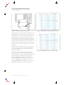
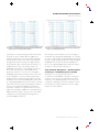
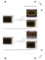
Technical Brief
Probe Bandwidth Calculations
A probe is a critical element in an oscilloscope
measurement system. An oscilloscope probe provides
the physical and electrical connection to the circuit
under test. It also buffers and conditions the signal
for the oscilloscope channel input. An ideal oscilloscope probe would measure a signal with perfect
fidelity so that it can be accurately displayed on the
attached oscilloscope. In making this measurement
the probe would also ideally not disturb the probed
signal in any way. Since ideal probes are only
available in an ideal world, here in the real world
probe measurement fidelity is limited by both probe
electrical performance and probe loading.
Every engineer has a story about a probe causing a
circuit to stop working. There are even stories about
probes that cause circuits to start working. The reality
is that probes interact with the devices under test
(DUT), and this interaction modifies the shape of the
signal waveform. One of the main goals in probe
design is to minimize the probe loading to such a
point that the interaction is insignificant to the device
under test. Unfortunately as signal speeds increase,
it becomes more difficult to reduce probe loading to
an insignificant level.
Probe Bandwidth Calculations
Technical Brief
Figure 1. Discrete
Model of Probe Loading.
Figure 2. Distributed
Model of Probe Loading.
Historically, oscilloscope probes have been described
using discrete models. A typical discrete model, as
shown in Figure 1, describes the probe loading as DC
resistance and an input capacitance.
on the physical properties of the material around the
transmission line. For a microstrip transmission line on
FR-4 circuit board material, the propagation velocity is
about 150 ps/inch, which is about half the speed of
light. For a signal rise time of 500 ps, the length of
transmission line over which the rise time variation of
the signal can be observed is about three inches
(electrical length = signal rise time/propagation
velocity). A conservative guideline that can be applied
is that an interconnect can be expected to show
transmission line effects for interconnects longer
than 1/6th the length over which the signal variation
propagates (0.5 inch for the microstrip transmission
line example)*1. As long as the physical characteristics
of the circuit are smaller than this 1/6th of a propagation
length, a discrete model can be used. However as
electrical interconnects get faster, this becomes much
more of an issue. A 100 ps rise time signal will have
a 0.66 inch propagation length in FR-4. Features
larger than 0.11 inches will start to show transmission
line effects.
This is a valid method when the signal speeds are
slow. Electrical signals will propagate down a transmission line with a propagation velocity that depends
Oscilloscope probes are now being described with
distributed models, as shown in Figure 2. These models
help to take into account transmission line effects.
Increasing signal speed for digital communications
has placed new demands on probe electrical performance and loading. High speed signal probing requires
an oscilloscope probe to measure signals in a transmission line environment. The effect of probe loading
in a transmission line environment requires a more
complex treatment than the simple discrete probe
load models once commonly used. Probe loading
effects in a distributed circuit environment have also
led a probe vendor to introduce a new approach to
both probe measurement and probe specification.
Because this new approach has created some
confusion in the probe market, this paper will examine
this new approach and compare it with the more
traditional, accepted approach.
Probe Loading
*1"TekConnect™ Probes: Signal Fidelity Issues and Modeling", Tektronix, Inc.
2
www.tektronix.com/accessories
Probe Bandwidth Calculations
Technical Brief
Probe loading can be more accurately characterized
by its input impedance over the frequency range of
the probe. Figure 3 shows the input impedance
variation with frequency of a high performance differential probe. The use of input impedance is a straightforward way to model complex interactions between
resistance, capacitance and inductance over frequency.
This characterization method allows probe users
to gauge the impact of the probe loading at
specific frequencies.
Oscilloscope Probing Philosophy
Oscilloscope probes have a very different usage
model when compared to oscilloscopes. Today’s high
bandwidth oscilloscopes all have 50Ω terminations on
each channel. The oscilloscope is meant to be used
as an end-of-line receiver that expects to see a signal
coming from a 50Ω source. An oscilloscope probe is
intended to be connected to a device under test that
is, presumably, already source and receiver terminated.
These probes are usually designed to have a high
input impedance so that the probe affects the device
under test as little as possible.
There are two schools of thought on what an oscilloscope
probe should actually display on an oscilloscope.
Tektronix subscribes to the philosophy that a probe
should measure the unloaded, or original, signal.
Agilent subscribes to a different philosophy that says
a probe should measure the loaded signal. What
exactly does this mean? First you have to understand
how probe bandwidth is characterized.
The through response, or transfer function, of a probe
is characterized as VOUT / VIN where VIN is the input to
the probe and the VOUT is the output of the probe. The
ratio describes the gain of the probe amplifier and
can be written as VOUT (f)/VIN(f) because this gain can
change with frequency. The bandwidth of the probe is
defined as the frequency at which the transfer function
of the probe is down to 0.707 (3dB) of its low frequency
Figure 3. Differential
Input Impedance of Tektronix P7380 with Short
Flex Small Resistor Flex Tip-Clip™ Assembly.
value. This is an industry standard definition of
bandwidth. The difference in implementation methodology between Tektronix and Agilent concerns the
definition of the reference signal, VIN. Introducing the
probe into that well controlled environment can cause
that environment to change. Tektronix and Agilent
account for that change in different ways.
Throughout the years, 50Ω environments have been
the standard for generation and transmission of high
speed signals. Consequently, oscilloscope probes
have been generally characterized using a terminated
50Ω signal generator. The response of a test signal
generator is calibrated to be as flat as possible over
the frequency range of interest. Tektronix characterizes
this flat source (VSOURCE) and calls it VIN. The
probe response is then designed to be as flat as
possible throughout its frequency range in this clean
50Ω environment. This method of characterizing
probes has an inherent effect of compensating for
the probe loading. A probe of this type displays the
original unloaded signal on the oscilloscope. This is
the signal the device under test would see before the
probe is attached.
www.tektronix.com/accessories
3
Probe Bandwidth Calculations
Technical Brief
Agilent takes the position that the loading of the probe
has an impact on the measured signal such that
VSOURCE ≠ VIN. They assert that the probe’s frequency
dependent loading has to be measured and factored
into the calibration to accurately derive the bandwidth
of the probe. A probe that has been characterized
with this method gives a bandwidth and probe
response that includes the loading of the probe in a
50Ω environment. This probe does not attempt to
compensate for the loading, but in fact includes
the loading. An Agilent probe displays on the
oscilloscope screen the original signal as it has
been loaded by the probe.
If a probe existed that had no loading, both philosophies
would converge and you would see no difference
between the probes. Since probe loading does exist,
the difference in measurement philosophy has an
impact on both the waveform displayed by the probe
and the specifications of the probe bandwidth.
To better explain the difference in philosophies, let
us look at a simplified example. Suppose you have a
perfect 1VDC signal that you want to measure. When
you measure this signal with a probe, you expect the
probe to measure 1VDC. If probe loading caused the
signal level to drop to 0.95V, would you want the
probe to read 1VDC or 0.95VDC? The Tektronix
philosophy is that you want to see a 1V signal.
Agilent’s philosophy is that you want to see the
0.95V signal.
This example can be taken one step further. Suppose
you want to measure a perfect AC sinusoidal 1Vpp
signal. This signal can be swept from a few hertz to
gigahertz frequencies and still have a perfect 1Vpp
signal level. As the signal source is swept through its
frequency range, should the probe output change with
frequency due to its changing load profile or should
the output of the probe read 1Vpp throughout the
4
www.tektronix.com/accessories
majority of its frequency range? This is a simplified
example, but it clearly illustrates the differences in
probing philosophy.
Tektronix believes that it is more useful for probe
users to know what is happening inside their circuits
when the probe is not attached. The remainder of this
paper examines in greater detail the effect of Agilent’s
probing philosophy and why Tektronix supports the
traditional bandwidth measurement technique.
How Probe Bandwidth is Measured
Tektronix designs the probe response to be as flat as
possible throughout its frequency range. This flatness
is tested with a Network Analyzer that has been
calibrated along with a probe test fixture to be a flat
source out to 20 GHz, as shown in Figures 4 and 5.
Network analyzers typically have special high
frequency coaxial connectors, so a special probe
calibration test fixture is used to connect the probe to
the network analyzer. The network analyzer is then
calibrated to take out any frequency effects of the
cables and the test fixture. This method insures the
repeatability of the measurement because there can
be slight differences in cables and fixtures between
test stations. This flat system is what Tektronix defines
as VSOURCE or VIN.
The probe is then connected to the test fixture, as
shown in Figure 6, and the response of the probe is
measured, as shown in Figure 7.
Probes have components that can be used to adjust
their frequency response. These components can be
actively adjusted to calibrate the probe in real time
and make the response as flat as possible throughout
its frequency range. One advantage of this method is
that the frequency dependant loading of the probe is
automatically compensated in the process.
Probe Bandwidth Calculations
Technical Brief
Probe Test Fixture
Figure 4. Network
analyzer and test fixture setup for test
system calibration.
Probe
Figure 5. After calibration, network analyzer showing
a flat Vsource.
Probe Power
Supply
Probe Test Fixture
50Ω
Termination
Figure 6. Setup
for measuring the probe response on the
Figure 7. Tektronix
P7380 Probe Response.
network analyzer.
www.tektronix.com/accessories
5
Probe Bandwidth Calculations
Technical Brief
Probe Test Fixture
Figure 8. Calibration
Setup to measure probe loading.
Figure 9. Loading
of Agilent 1134A with Differential Solder Probe Tip.
Agilent follows a somewhat similar method, but uses a
few additional steps to calibrate the probe to show a
loaded response. After the network analyzer has been
calibrated as a flat source with the test fixture, the
probe loading over frequency is measured and saved
to memory. This is done by measuring the test fixture
through response with the probe connected to the test
fixture, as shown in Figure 8. The result of the probe
loading on the test fixture through response is shown
in Figure 9.
Math is then used to divide the flat reference by the
probe loading to account for the affects of loading.
This is what Agilent uses as VIN when they do the
bandwidth calculation.
Then the probe is placed into the system and its
frequency response is measured. Figure 11 shows
the Agilent probe response using the traditional bandwidth measurement used by Tektronix. Figure 12
shows the Agilent probe response using the new
Agilent bandwidth measurement method. It can be
seen by comparing the two figures that the new
Agilent bandwidth method tends to inflate the probe
bandwidth compared to the traditional method.
6
www.tektronix.com/accessories
Figure 10. Calculated VIN using
math to account for probe loading.
Probe Bandwidth Calculations
Technical Brief
Figure 11. 1134A
Differential Solder Probe Tip Response without using
math to divide out the loading (Tektronix Method).
If the probe is measured using the Tektronix method,
the probe response exhibits about a 2dB roll-off
starting around 2 GHz. Once the loading is divided
from the probe response, the probe looks fairly flat
throughout its frequency range. The Agilent probes
are designed to give a math frequency response, or
loaded response, that is as flat as possible. The
bandwidth of the probe is then defined as the point
where this math response is down 3dB from the
probe’s DC response. In essence the new Agilent
bandwidth specification method assumes a zero ohm
source impedance, a source unaffected by probe
loading. A probe characterized by Agilent’s method
would have an effective bandwidth that is lower than
its calculated bandwidth because the probe is used in
real world environment with real impedances that are
not zero. The Tektronix bandwidth measurement
method by comparison is optimized for an effective
25Ω source impedance (50Ω source in parallel with a
50Ω termination), which is much closer to real world
conditions for measuring high speed signals in a
terminated 50Ω environment.
Figure 12. 1134A Differential Solder Probe Tip Response using math to
divide out the loading (Agilent Method).
One indication of the limitations of this new Agilent
method for specifying probe bandwidth is to consider
the case of a probe with a high bandwidth and a large
amount of probe loading. This probe, using the Agilent
bandwidth measurement method, would appear to
have a very high bandwidth, but would have limited
usefulness in a real world environment.
Time Domain Response - Ramifications
of Using a Loaded Response Probe
Although one of the main specifications for
oscilloscopes is bandwidth, a measure of frequency
response, oscilloscopes are primarily time-domain
instruments. The data displayed on an oscilloscope
is a graph of amplitude versus time. Differences that
look small in the frequency domain can have a big
impact in the time domain.
www.tektronix.com/accessories
7
Probe Bandwidth Calculations
Technical Brief
Unloaded Eye Pattern from Source*
Figure 13. Time
Domain effect of probe loading as shown on the CSA/TDS8000 sampling oscilloscope. *2.5 Gb/s PRBS7 data pattern, 40 ps 10/90% Rise time
A square wave is much more complex than it looks
when seen on an oscilloscope display. According to
Fourier math, a perfect square wave can be broken
down into an infinite series of harmonic sinusoids.
However, since today’s probes and oscilloscopes do
not have an infinite amount of bandwidth, a square
wave signal will not appear perfect. Since the square
wave signals cannot change instantly from a low state
to a high state, rise time and fall time numbers are
used to characterize the speed of this change. More
high frequency content equates to faster rise and
fall times. The sharpness of the square wave signal
edges is affected by the amount of high frequency
content that is available. Probe loading is frequency
dependant and it typically gets worse at higher
frequencies. Therefore probe loading has a direct
impact on the corner of any step function or square
wave. Figure 13 illustrates the probe loading affects
on an eye diagram.
The differences between the two philosophies of
showing either the unloaded response (Tektronix) or
the loaded response (Agilent) become much more
apparent in the time domain.
8
Loaded Eye Pattern
www.tektronix.com/accessories
How the Theory is Reduced to Practice
As shown in Figures 14 and 15, both measurement
methodologies produce what they promise. The
Tektronix probe was designed to show the original
signal that was output by the device under test before
the probe was attached. Even for a signal with this
fast rise time, the response shown on the oscilloscope
display looks very similar to the eye diagram generated
by the source. The Agilent probe was designed to
show the loaded signal, the signal in the device under
test after the probe was attached. The response on
the Agilent oscilloscope display does have similar
features to the loaded eye pattern.
Both methods for calibrating the probes are valid,
depending on what you want to look at and measure.
Tektronix believes that most probe users want to know
what is happening inside their circuits when a probe
is not attached. Therefore the probes are designed
to meet that need. If you want to know what is
happening inside the circuit, you should choose a
Tektronix probe. This type of probe is a good general
purpose tool for making measurements without a lot
of effort.
Probe Bandwidth Calculations
Technical Brief
Tektronix P7380 Probe Response
on TDS6804B Oscilloscope
Unloaded Eye Pattern from Source*
Loaded Eye Pattern
Figure 14. Example
of an unloaded response type probe in the time domain. *2.5 Gbps PRBS7 data pattern, 40 ps 10/90% Rise time
Agilent 1134A Differential Probe Tip
Response on 54855A Oscilloscope
Unloaded Eye Pattern from Source*
Loaded Eye Pattern
Figure 15. Example
of a loaded response type probe in the time domain. *2.5 Gbps PRBS7 data pattern, 40 ps 10/90% Rise time
www.tektronix.com/accessories
9
Probe Bandwidth Calculations
Technical Brief
If you want to see how the probe is affecting your
circuit, you should consider choosing an Agilent probe.
For example, this is useful if the circuit can be modeled
and simulated. The probe loading can be added to
the model and the output of the simulation can be
checked with the output of probe and oscilloscope.
A Tektronix probe can be used for this type of
measurement, but it requires that the device under
test be terminated into an oscilloscope channel,
typically through a coax cable. This type of connection
is not always available on circuit boards.
An Agilent probe is good in a few specific applications,
but it does not work very well as a general purpose
tool. The probe will not give you the data you are
looking for without a lot of auxiliary calculation and
extra time because the loading of the probe is always
included in the data. This type of probe is not a
good general purpose tool because it adds an extra
layer of complexity.
Engineers know what they expect to see when they
measure their circuits and they use probes to verify
that everything is working as designed. The Agilent
probe will only show the system performance as it is
affected by the probe loading. Engineers then have
to decide if what they are seeing is due to their
system or just part of the effect of probe loading. It is
possible to take the data and work backwards to find
the original signal, but this process is difficult and
time consuming. Agilent has no automated oscilloscope routine that will perform this step. It must be
done for every single waveform that is measured. If
this step is omitted, then the data that is recorded is
suspect. This phenomenon can become even more of
a issue if engineers want to use one of the vast array
of applications that are available on oscilloscopes.
10 www.tektronix.com/accessories
All of theses applications use the oscilloscope data
to perform their analysis. If the raw probe data is
used, the applications may give false passes or fails
because of the extra effects from the probe that are
not there in the original signal.
Agilent has an application note that describes in more
detail methods that can be used to take the output of
their probe and work backwards to display the original
signal. Agilent sampling oscilloscopes have a normalization feature that can be used to calibrate out test
fixture features when making time-domain reflectometer
(TDR) measurements. This same normalization feature
can be used to account for the probe loading and helps
the probe display the original signal. The drawback to
this method is that the source needs to be well characterized with the probe loading in place before the
normalization can occur. In many instances, the probe
user’s final goal is to characterize their own signal.
Why go through all the trouble to fully characterize
their signal so that they can go back and measure it
again with the probe? Agilent’s real time oscilloscopes
do not have this normalization feature. Their solution
to this problem is to add a probe compensation circuit
to the source using discrete components. While this
does produce the desired effect, it is an impractical
solution for engineers testing their own circuits. Why
go through all the trouble to back out the original
signal from the Agilent probe when a Tektronix probe
does this directly?
Another drawback of an Agilent probe is that it
cannot be reliably used for mask testing. As can
be seen in the pictures, probe loading can have a
significant impact on the front corner of high speed
digital signals. This could cause a signal to artificially
fail or pass a mask test because the probe loading is
part of the response.
Probe Bandwidth Calculations
Technical Brief
Mask testing is an important tool for high speed serial
data testing. Most serial data standards specify
masks that may be used to validate data streams to
make sure they comply to the standards. The masks
are typically designed to be used with an end-of-line
receiver, like a terminated 50Ω oscilloscope channel
or an SMA-input probe like the P7380SMA. End-of-line
receivers do not have to deal with the issues of probe
loading. The signal quality that reaches the receiver
depends mainly on the quality of the transmission
lines and the 50Ω termination. The masks define the
limits of a serial data stream in its intended environment,
which does not include external factors like probe
loading. Sometimes it is not possible to gain access
to a serial data stream to pipe it directly into an
oscilloscope. An example of this situation would be
two chips on the same board that have a high speed
serial connection between them. The only way to
gain access to the data stream would be to use an
oscilloscope probe.
A Tektronix probe can be used for mask testing
because the probe is designed to reproduce the
signal as it was in its original environment. On the
other hand, an Agilent probe displays a signal that
includes the probe loading and may not meet the
criteria to make a valid mask test. A circuit that is
designed to pass a mask test with an Agilent probe
may experience problems when the probe is not
connected to the system, because it passed the test
in a non-valid environment. An Agilent probe may be
used to make compliance tests if special modified
masks are used, but standard masks as specified by
the standard committees cannot be used.
The Agilent probe’s rise time measurements may also
be invalid because the probe’s loading affects the
front corner of any step response. The probe
response that is displayed on the oscilloscope screen
includes the loading. Oscilloscope measurement
algorithms are typically designed to look for a 10-90%
point to make its measurement. Distortion in the front
corner may change the wave shape enough that the
90% point is significantly different and measures
incorrectly. 20-80% rise time measurements experience
less of an impact from front corner distortions
because the measurement takes place farther from
the corner.
Conclusion
An oscilloscope probe is a tool used by engineers to
quickly make measurements and help get products to
market. The enormous increase in signal speeds over
the past few years has introduced complexities in
probing that probe users need to know about and
account for. In the past, all oscilloscope probe
designers subscribed to the same philosophy. The
introduction of Agilent’s loaded response type probe
has given probe users an extra tool, but it has also
caused some confusion.
Care must be taken to understand how a probe will
interact with a DUT, no matter which probe type is
used. Agilent probes might be good tools for a small
set of applications, but are not well suited for general
purpose probing tasks like DUT characterization,
validation, and mask testing because they require
extra calculation to extract the probe loading. In
contrast, Tektronix probes are good tools
for general purpose probing tasks because they
endeavor to directly show the original, unloaded signal.
www.tektronix.com/accessories
11
Sources:
"Z-Active™: A New High Performance Probe
Architecture", Tektronix, Inc.
Contact Tektronix:
ASEAN / Australasia / Pakistan (65) 6356 3900
Austria +41 52 675 3777
Balkan, Israel, South Africa and other ISE Countries +41 52 675 3777
"ABC's of Probes", Tektronix, Inc.
Belgium 07 81 60166
Brazil & South America 55 (11) 3741-8360
Canada 1 (800) 661-5625
"Side-by-Side Comparison of Agilent and Tektronix
Probing Measurements on High-Speed Signals",
Agilent App Note 1491 Agilent Technologies, Inc.
Central Europe & Greece +41 52 675 3777
Central East Europe, Ukraine and Baltics +41 52 675 3777
Denmark 80 88 1401
Finland +41 52 675 3777
"Time-Domain Response of Agilent InfiniiMax Probes
and 54850 Series Infiniium Oscilloscopes",
Agilent App Note 1461 Agilent Technologies, Inc.
France & North Africa +33 (0) 1 69 81 81
Germany +49 (221) 94 77 400
Hong Kong (852) 2585-6688
India (91) 80-22275577
Italy +39 (02) 25086 1
User Manual: 1134A 7 GHz InfiniiMax Differential
and Single-ended Probes (Publication Number
01134-97007), Agilent Technologies, Inc.
Japan 81 (3) 6714-3010
Luxembourg +44 (0) 1344 392400
Mexico, Central America & Caribbean 52 (55) 56666-333
Middle East, Asia and North Africa +41 52 675 3777
The Netherlands 090 02 021797
Norway 800 16098
People’s Republic of China 86 (10) 6235 1230
Poland +41 52 675 3777
Portugal 80 08 12370
Republic of Korea 82 (2) 528-5299
Russia, CIS & The Baltics 7 095 775 1064
South Africa +27 11 254 8360
Spain (+34) 901 988 054
Sweden 020 08 80371
Switzerland +41 52 675 3777
Taiwan 886 (2) 2722-9622
United Kingdom & Eire +44 (0) 1344 392400
USA 1 (800) 426-2200
USA (Export Sales) 1 (503) 627-1916
For other areas contact Tektronix, Inc. at: 1 (503) 627-7111
Updated November 3, 2004
For Further Information
Tektronix maintains a comprehensive, constantly expanding collection of
application notes, technical briefs and other resources to help engineers
working on the cutting edge of technology. Please visit www.tektronix.com
Copyright © 2004, Tektronix, Inc. All rights reserved. Tektronix products are covered by U.S. and foreign
patents, issued and pending. Information in this publication supersedes that in all previously
published material. Specification and price change privileges reserved. TEKTRONIX and TEK are
registered trademarks of Tektronix, Inc. All other trade names referenced are the service marks,
trademarks or registered trademarks of their respective companies.
11/04 FLG/WOW
60W-18324-0