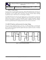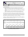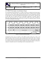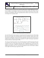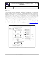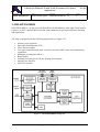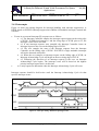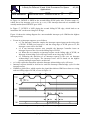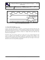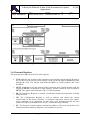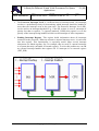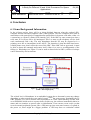
1
A Study On Different 32 and 16-bit Processors For Space Applications By Krister Sundström Wilh. Sonesson AB Kiruna Sweden June 2000 Date: 2000-06-20 00:45 Prepared By: Krister Sundström Approved By: Checked By: Copyright 2000 by µConos A Study On Different 32 and 16-bit Processors For Space Applications 2 (62) Prepared By Created Last Saved Rev Version Krister Sundström 2000-06-20 04:16 2000-06-20 04:16 D 5 DOCUMENT Change Record Changes between issues are marked with a left-bar. Issue D1 D2 Date Paragraphs affected 2000-03-10 All 2000-04-02 All D3 D4 2000-04-10 3.1, 3.2, 3.3, 3.4 2000-04-11 3.1, 3.2, 3.3, 3.4 D5 2000-06-14 3.2, 3.3, 6f Change information New document Split the document into smaller subdocuments to avoid big and heavy treatable files while editing. Sub-documents can be found in the directories with the same name as the processors. This document is a cut&paste version of the whole processor document. Do NOT edit in this file. Merged all sub-documents. Document split. Word is too buggy even to handle sub-documents. It has come to our knowledge that ERC32 is NOT open-sourced after all. Recommending Leon as supplement. Copyright 2000 by µConos A Study On Different 32 and 16-bit Processors For Space Applications 3 (62) Prepared By Created Last Saved Rev Version Krister Sundström 2000-06-20 04:16 2000-06-20 04:16 D 5 Abstract This is the document for the Master’s Thesis “A study on on-board computer systems for micro satellites in low-earth orbit constellations” at the Department of Space Physics, Umeå University, Sweden. Four processors for space applications are studied: RH-THOR, ERC32, LEON, and HS-RTX2010RH. The background data for the mission study is a low-earth orbit around 400-600 km, short lifetime (3 years), and small satellites (around 60 kg). With the processor characteristics listed herein this document, Leon is recommended for the LEO constellation. Leon is an open-sourced processor where the VHDL code can be modified and optimised for best performance. In addition, other functionalities can be added. Detta är dokumentet från mastersavhandlingen ”A study on on-board computer systems for micro satellites in low-earth orbit constellations” vid Rymdfysikinstitutionen, Umeå Universitet. Följande fyra processorer har studerats: RH-THOR, ERC32, LEON och HSRTX2010RH. Data som ligger till grund för beslut är low-earth orbit på omkring 400-600 km, kort livstid (tre år) och småsatelliter (ca 60 kg). Med de processorkarakteristika som är listade i dokumentet rekommenderas att Leon används för LEO-konstellationen. Största anledningen är de stora möjligheterna till modifikationer som den öppna källkoden ger. VHDL-koden kan optimeras för bästa prestanda på just dessa satelliter och övriga funktionaliteter kan läggas till. Copyright 2000 by µConos A Study On Different 32 and 16-bit Processors For Space Applications 4 (62) Prepared By Created Last Saved Rev Version Krister Sundström 2000-06-20 04:16 2000-06-20 04:16 D 5 Table of Contents ABSTRACT ..............................................................................................................................3 INTRODUCTION ....................................................................................................................6 1 DOCUMENTS .......................................................................................................................7 1.1 APPLICABLE DOCUMENTS .................................................................................................7 1.2 ABBREVIATIONS ................................................................................................................8 2 PROCESSORS FOR SPACE APPLICATIONS..............................................................12 2.1 WHAT IS A REAL-TIME SYSTEM? ...................................................................................14 3 A CLOSER LOOK ON THE PROCESSORS..................................................................16 3.1 RH THOR.......................................................................................................................16 3.1.1 Addressing ...............................................................................................................16 3.1.2 Initialisation .............................................................................................................17 3.1.3 Thor Pipeline ...........................................................................................................17 3.1.3.1 Instruction Fetch ...............................................................................................17 3.1.3.2 Address Generation ..........................................................................................17 3.1.3.3 Operand Fetch...................................................................................................18 3.1.3.4 Execute Stage ...................................................................................................18 3.1.4 Error correction and control ....................................................................................18 3.1.5 Memory Protection ..................................................................................................19 3.1.6 Real-Time Clock......................................................................................................19 3.1.7 Exceptions ...............................................................................................................19 3.1.8 Tasking ....................................................................................................................20 3.1.9 RH THOR Conclusions ...........................................................................................20 3.2 ERC32 ............................................................................................................................21 3.2.1 ERC32 - The idea ....................................................................................................22 3.2.2 ERC32 Memory Controller Unit .............................................................................23 3.2.3 ERC32 Integer Unit .................................................................................................24 3.2.4 ERC32 Registers......................................................................................................25 3.2.4.5 ERC32 Register Windows................................................................................26 3.2.5 ERC32 Atom Action .................................................................................................28 3.2.5 ERC32 Atom Action ...............................................................................................29 3.2.6 ERC32 Pipeline and Instruction Executing Timing ................................................29 3.2.6.6 Instruction stages ..............................................................................................30 3.2.7 ERC32 Interrupts (Asynchronous Traps) ................................................................31 3.2.8 ERC32 Conclusions.................................................................................................33 3.3 LEON ...............................................................................................................................34 3.3.1 Leon Integer Unit.....................................................................................................36 3.3.1.7 Leon Instruction Pipeline..................................................................................37 3.3.1.8 Leon Floating Point Unit ..................................................................................37 3.3.2 Leon EDAC .............................................................................................................38 Copyright 2000 by µConos A Study On Different 32 and 16-bit Processors For Space Applications 5 (62) Prepared By Created Last Saved Rev Version Krister Sundström 2000-06-20 04:16 2000-06-20 04:16 D 5 3.3.3 Leon Interrupts ........................................................................................................39 3.3.4 Leon Timer Unit ......................................................................................................40 3.3.5 Leon UART .............................................................................................................41 3.3.6 Leon Parallel I/O Port..............................................................................................41 3.3.7 Leon Power Down ...................................................................................................42 3.3.8 Leon Conclusions ....................................................................................................42 3.4 HS-RTX2010RH ............................................................................................................43 3.4.1 Interrupts..................................................................................................................44 3.4.2 HS-RTX2010RH Operation ....................................................................................46 3.4.3 Internal Registers .....................................................................................................47 3.4.4 On-Chip Peripheral Registers ..................................................................................48 3.4.4.9 Timer/Counter registers:...................................................................................48 3.4.4.10 MAC registers: ...............................................................................................48 3.4.4.11 Interrupt Controller Registers.........................................................................48 3.4.4.12 Stack controller register..................................................................................49 3.4.5 HS-RTX2010RH Conclusions ................................................................................49 4 GENERAL TERMS ............................................................................................................50 4.1 INTERRUPT REGISTERS .....................................................................................................50 5 PROCESSOR COMPARISON ..........................................................................................52 6 CONCLUSION ....................................................................................................................54 6.1 SOME BACKGROUND INFORMATION ................................................................................54 6.2 CHOOSING PROCESSOR ....................................................................................................59 I. APPENDIX A – PARASITIC SILICON CONTROL RECTIFIERS .......................61 7 REFERENCES ....................................................................................................................62 Copyright 2000 by µConos A Study On Different 32 and 16-bit Processors For Space Applications 6 (62) Prepared By Created Last Saved Rev Version Krister Sundström 2000-06-20 04:16 2000-06-20 04:16 D 5 Introduction This study briefly lists four different processor architectures, what peripherals they fully support by default, and possible memory bank sizes. The four processors are RH-THOR, ERC32, LEON, and HS-RTX2010RH. Special characteristics for the processors are listed as well. As different processors have their own specialities it is sometimes difficult to compare the processors. In the last chapter, a recommendation is presented on which processor to use for the uConos satellite constellation. Chapter 1 lists some applicable document whilst chapter 2 briefly lists what a Real-Time System is. The different processors are studied in sections 3.1 (RH THOR), 3.2 (ERC32), 3.3 (Leon), and 3.4 (HS-RTX2010RH). Important registers and functionalities as well as processor architectures are explained in these sections. Chapter 4 briefly explains to most common interrupt register. The different processors are listed with some advantages and disadvantages in chapter 5. Chapter 6 gives a more detailed explanation of why Leon is chosen as the OBC processor. Chapter I is an appendix and finally chapter 7 holds a list of references. The document reader is assumed to have brief knowledge in Real-Time Systems (RTS) and the Ada programming language. Copyright 2000 by µConos A Study On Different 32 and 16-bit Processors For Space Applications 7 (62) Prepared By Created Last Saved Rev Version Krister Sundström 2000-06-20 04:16 2000-06-20 04:16 D 5 1 Documents 1.1 Applicable Documents RTSAPL Real-Time Systems and Programming Languages Alan Burns, Andy Wellings. Addison-Wesley(40365) ISBN:0-201-40365-X WCFEFS Working Copy for Electronics In Space Unpublished document written by Laila Andersson, IRF-Kiruna, Sweden November 1999 RHTIS Rad Hard Thor Instruction Set Architecture Saab Ericsson Space document P-TOR-NOT-0001-SE Prepared by Stefan Asserhäll, 2 Feb 1999 TSC691E User’s Manual for ERC32 Integer Unit Temic Semiconductors, http://www.temic-semi.de/nt/ams/ October 9, 1996 TSC692E User’s Manual for ERC32 Floating Point Unit Temic Semiconductors, http://www.temic-semi.de/nt/ams/ December 2, 1996 TSC693E User’s Manual for ERC32 Memory Controller Temic Semiconductors, http://www.temic-semi.de/nt/ams/ April 10, 1997 ALASP Assembly Language and System Programming for the 68k Family William Ford, William Topp. 2nd edition ISBN: 0-669-28199-9 SDH Spacecraft Data Handling. Teacher’s notes by Torbjörn Hult Saab Ericsson Space, version 991117TH Observational Platforms Course at the Space Engineer Campus, Sweden RHTD Radiation Hardened Thor Documentation and Specifications Saab Ericsson Space, http://www.space.se Copyright 2000 by µConos A Study On Different 32 and 16-bit Processors For Space Applications 8 (62) Prepared By Created Last Saved Rev Version Krister Sundström 2000-06-20 04:16 2000-06-20 04:16 D 5 1.2 Abbreviations ADC AEE AG ALU Am. Ann. AOCS Assoc. ATM Analogue to Digital Converter Address Error Exception Address Generation Arithmetic Logic Unit American Annual Attitude and Orbit Control System Association Asynchronous Transfer Mode bps BOC BOS Bull. bits per second Beginning Of Code Beginning Of Stack Bulletin CB CL Conf. Comm. CCC Conf. CR CWP Check Bit Current Limiter Conference (on) Communications (of) Communication, Command, and Control Conference Configuration Register Current Window Pointer DAC DEC Dept. DHU DR DSP DMM Digital to Analogue Converter Decoder Department (of) Data Handling Unit Delay Register Digital Signal Processor Digital Multimeter ed. EEPROM, E2PROM EI EIB Eng. ENC EOC EOS ER ES ESA edition, editor Electrically Erasable PROM External Interrupt Exception Information Block Engineering Encoder End Of Code End Of Stack Exception Register Execute Stage European Space Agency Copyright 2000 by µConos A Study On Different 32 and 16-bit Processors For Space Applications 9 (62) Prepared By Created Last Saved Rev Version Krister Sundström 2000-06-20 04:16 2000-06-20 04:16 D 5 FAR Fed. FIFO FPE FPT Failing Address Register Federal First In First Out Floating Point Exception Floating Point GEO Gb GB Gibi Giby Govt. GPS Geostationary Orbit Gigabit = 1000 Mb Gigabyte = 1000 MB 1024 Mibi 1024 Miby Government Global Positioning System h/w hardware IAC IBC ICD ICR ICU i/f IF IFR II ILR IMR Inst. Int’l INTSUP IP IR IRL IRQ ISL IVR Interrupt Acknowledge Cycle Interrupt Base Register Interfacing Control Document Interrupt Controlling Register Interrupt Controller Unit interface Instruction Fetch Interrupt Force Register Internal Interrupt Interrupt Level Register Interrupt Mask Register Institute International Interrupt Suppress Internet Protocol Instruction Register Interrupt Request Level Interrupt Request Inter/Intra Satellite Link, Intersatellite Communciation Interrupt Vector Register J. Journal (of) kb kB Kibi Kiby Kilobit = 1000 Bits Kilobyte = 1000 Bytes 1024 bits 1024 * 1024 bits Copyright 2000 by µConos A Study On Different 32 and 16-bit Processors For Space Applications 10 (62) Prepared By Created Last Saved Rev Version Krister Sundström 2000-06-20 04:16 2000-06-20 04:16 D 5 LEO LIFO LSb LSB LSW LZD Low-altitude Earth Orbit Last In First Out Least Significant Bit Least Significant Byte Least Significant Word Leading Zero Detector MAC Math. Mb MB Mibi Miby MPC MSb MSB MSR MSW Multiplier-Accumulator Mathematics, Mathematical Megabit = 1000 kb Megabyte = 1000 KB 1024 kibi 1024 kiby Memory Page Controller Most Significant Bit Most Significant Byte Memory Status Register Most Significant Word NAT Nat’l NMI No. NOP Network Adress Translation National Non-Maskable Interrupt Number No OPeration OBC OBP OBT OF OH OS On-Board Computer On-Board Processing On-Board Timer Operand Fetch Overhead Operating System PC PCNN PIR P/L PR Proc. PROM PSR PTP Program Counter Pulse-Coupled Neural Network Pending Interrupt Register Payload Prescaler Reload Proceedings (of) Programmable Read Only Memory Processor State Register Point-To-Point Rev. r/h, RH Review Radiation Hard(ened) Copyright 2000 by µConos A Study On Different 32 and 16-bit Processors For Space Applications 11 (62) Prepared By Created Last Saved Rev Version Krister Sundström 2000-06-20 04:16 2000-06-20 04:16 D 5 RISC RTOS RTS RTU Reduced Instruction Set Computer Real-Time Operating System Real-Time System Remote Terminal Unit S/C, s/c SBE SCR SEE SGM SIB Soc. SOI SP SPARC SPM SRR SSR s/w Symp. Spacecraft, Satellite Single Bit Error Silicon Control Rectifier Storage Error Exception Safe Guard Memory Startup Information Block Society Silicon On Insulator Stack Pointer Scalable Processor Architecture Solar Panel Motor Status Register Step Square Root software Symposium (of or on) TCB TCB TCP TCR Task Control Blocks Test Check Bits Transmission Control Protocol Timer Control Register Temics, TS TIB TOS TPR TR Trans. Temic Semiconductors Task Information Block Top Of Stack Pointer Timer Preload Register Task Register Transactions (on) UART Univ. Universal Asynchronous Receiver Transmitter University Vol. Volume w/d, WD w/s, WS WIM Watchdog wait state(s) Window Invalid Mask Copyright 2000 by µConos A Study On Different 32 and 16-bit Processors For Space Applications 12 (62) Prepared By Created Last Saved Rev Version Krister Sundström 2000-06-20 04:16 2000-06-20 04:16 D 5 2 Processors for space applications The processor in this space application is responsible for running the mission software and interfacing to nearby peripherals. Mission software includes, among other tasks, attitude and orbit control, software telemetry formatting, and housekeeping. Examples of peripherals are memory, bus controller(s), telemetry controlling, telecommand distribution, etc. An Operation System (OS) is preferable to handle different software tasks and timing constraints. The OS used must be a Real-Time OS (RTOS) to be able to handle all services needed in the mission software. Time tagged instructions are commonly used to perform either periodic or sporadic instructions. The time queue is extra useful when the satellite is out of sight for any ground station. When performing attitude and orbital corrections, timing is of great importance when controlling the actuators. In small satellite systems, like uConos, the central processing unit (OBC) is tightly coupled to the data-handling unit (DHU) and sometimes they are gathered under the same name. Called either the OBC or the DHU. In this study, they are seen as a common system gathered under the name OBC, see Figure 1 for an example of an OBC/DHU. Important issues for the platform on-board computer system can be: • Processing of uplink telecommand (TC) data stream o Assemble, decode, and distribute incoming telecommands • Generate downlink telemetry (TM) data stream o Collect telemetry data o Generate TM Frames • Provide general I/O for command distribution and telemetry data collection • Provide processing power for various tasks o Battery charging control o Thermal control o Antenna pointing (attitude controlling) o Payload control • Provide with timing functionalities o On-Board Timer (OBT) counter o Time pulse synchronising, by using GPS receivers o Distribution of synchronisation signals • Provide with autonomy functionalities o System supervision and context switching (OS aspects) o Automatic system reconfiguration in case of system error(s) Copyright 2000 by µConos A Study On Different 32 and 16-bit Processors For Space Applications 13 (62) Prepared By Created Last Saved Rev Version Krister Sundström 2000-06-20 04:16 2000-06-20 04:16 D 5 Figure 1 - A Typical Data Handling System Copyright 2000 by µConos A Study On Different 32 and 16-bit Processors For Space Applications 14 (62) Prepared By Created Last Saved Rev Version Krister Sundström 2000-06-20 04:16 2000-06-20 04:16 D 5 2.1 What Is A Real-Time System? A real-time system (RTS) is a system that not only performs the right functionality but also performs the functionality at the right time. A system may have to answer to an external event within a predefined time interval. [RTSAPL] has the following definition: “The correctness of a real-time system depends not only on the logical result of the computation but also on the time at which the results are produced.” Real-time systems are said to be either hard or soft. Soft real-time systems are those where response times are important but the system will still function correctly, with some possible degradation, if deadlines are occasionally missed. An example of a soft real-time system can be sampling of scientific data where temporary loss of data can be allowed. Hard real-time systems though, are systems where a catastrophe can follow if a deadline is missed. A classical example is an aircraft. If the system that controls the avionics fails to respond to an external event, the aircraft may crash. In space applications, similar scenario can occur if the satellite is drifting so the solar panels will turn away from the sun and loosing power. The satellite must turn back the solar panels in the correct direction before the battery power goes too low to drive the Solar Panel Motor (SPM). Of course, there are different time periods between the catastrophes in the different scenarios but the deadline is still hard for both systems. One service may have both soft and hard deadlines. For example, a response to some warning event may have a soft deadline of 50 ms (for an optimally efficient reaction) and a hard deadline of 200 ms (to guarantee that no damage to equipment or personnel takes place). The solar panel scenario can also be seen as a mixed hard and soft system. The instant pointing can be seen as soft. The satellite still has electric power from the batteries to adjust the attitude of the satellite if drifting, but it has to be corrected before the battery runs out of power (hard). To build an efficient real-time system, one either needs a hardware (processor) that supports task and context switching or a programming language that implements the switching in the run-time code (RTOS). Systems consisting of a combination of the hardware and software support exist. ADA95 is one language that supports real-time kernels and is a commonly used programming language in the space industry, as it is very strict in general and it is almost impossible to make any conversions errors, using faulty pointers and so forth. This is the language to be used in the continuation of the Conos Project. Copyright 2000 by µConos A Study On Different 32 and 16-bit Processors For Space Applications 15 (62) Prepared By Created Last Saved Rev Version Krister Sundström 2000-06-20 04:16 2000-06-20 04:16 D 5 The processors in this study are listed in Table 1: Processor RH THOR ERC32 LEON HS-RTX2010RH Manufacturer Saab Ericsson Space (SES) Temic Semiconductors ESA Harris (HS) Table 1 - Some processors for space use Copyright 2000 by µConos A Study On Different 32 and 16-bit Processors For Space Applications 16 (62) Prepared By Created Last Saved Rev Version Krister Sundström 2000-06-20 04:16 2000-06-20 04:16 D 5 3 A closer Look On The Processors The processors are briefly presented in the following subsections and material that is essential for the processor choice phase are also listed and briefly explained. Commonly used registers will be listed in section 4. 3.1 RH THOR The radiation hardened Thor processor is a single 32-bit, four stage piped RISC (Reduced Instruction Set Computer) processor. Instead of using traditional registers, Thor uses stackoriented instruction sets. Instructions for both integers and IEEE-754 floating-pointers are supported. Thor is designed to provide hardware support for the Ada programming language to allow fast task rendezvous and low interrupt latency using the Ada tasking mechanism and also to simplify exception detection and handling, thus speeding up many runtime checks. For applicable documents, see [RHTD]. 3.1.1 Addressing The total memory address space for Thor is 2 Giby. OP-code size is always a multiple of 16 bits in length and therefore all instructions are addressed with a half word address, where each half word is 16 bits (2 bytes). Data is addressed with a full word address, where each word is 32 bits. The memory is split into two halves, each with a 1 Giby address space. The lower memory half uses the data error checking, can be cached, and is affected by the Configuration Register w/s settings. The upper half is intended for memory mapped I/O and memory expansion, cannot be cached, has no error checking and w/s are determined using the Chip Ready signal. Memory storage uses the little-endian storage. I.e., the least significant byte is stored at the lowest address and the most significant byte on the highest memory address. Stored Number 0x12345678 (32-bit) 0x1234, 0x5678 (16-bit) Stored In Big-Endian 12 34 56 78 12 34 56 78 Copyright 2000 by µConos Stored In Little-Endian 78 56 34 12 34 12 78 56 A Study On Different 32 and 16-bit Processors For Space Applications 17 (62) Prepared By Created Last Saved Rev Version Krister Sundström 2000-06-20 04:16 2000-06-20 04:16 D 5 3.1.2 Initialisation There is a Startup Information Block (SIB) in memory, addressed when the chip START signal is set, which initialises necessary registers in the microprocessor after a reset. The registers initialised are Program Counter (PC), Top Of Stack Pointer (TOS) and Configuration Register (CR), see Table 2. Address 0x00000000 0x00000004 0x00000008 Register PC TOS CR Table 2 - Startup Information Block 3.1.3 Thor Pipeline 3.1.3.1 Instruction Fetch The Instruction Fetch (IF) stage has two instruction pre-fetch queues, with three 32-bit words each, to allow Thor to pre-fetch instructions. The IF stage reads instructions into the prefetch queues, either from memory or from the instruction cache. When the pipeline is not stalled, the IF stage sends the next instruction to the AG stage and increments the Program Counter (PC). When a control transfer instruction is executed, the PC is loaded with the target address, and the pre-fetch queues are switched. 3.1.3.2 Address Generation The Address Generation (AG) stage computes two addresses, and updates the Top Of Stack (TOS) register. The source address is used by the OF stage to fetch the data operand. The destination address is used to store the result computed by the EX stage. The two addresses are computed relative to the TOS or PC when addressing data, and relative to the Task Pointer (TP) register when dispatching a new task. Address computations utilizing the TOS register use what is termed indirect delayed addressing. This means that the indirect address, stored in the TOS, is computed in the EX stage. This computation must be completed two instructions prior to the instruction using the address (in TOS) for its source or destination address. The AG stage performs checks on the computed addresses, to ensure that TOS relative addresses are within the limits set by the Beginning Of Stack (BOS) and End Of Stack (EOS) registers, and that program code delimited by Beginning Of Code (BOC) and End Of Code (EOC) is not changed. An exception will be raised if a violation is detected. Copyright 2000 by µConos A Study On Different 32 and 16-bit Processors For Space Applications 18 (62) Prepared By Created Last Saved Rev Version Krister Sundström 2000-06-20 04:16 2000-06-20 04:16 D 5 3.1.3.3 Operand Fetch The Operand Fetch (OF) stage fetches the instruction operand pointed out by the source address provided by the AG stage, if required. The operand may either be fetched from memory or the data cache, or be the instruction parameter. The operand is passed from the OF stage to the EX stage, along with the destination address. 3.1.3.4 Execute Stage The Execute Stage (ES) executes instructions, using the ALU, the Multiplier and the Barrel Shifter, to compute logical and integer, as well as IEEE-754 floating-point data. The result produced is generally placed in the TOP register and written to the destination address, either to the cache or directly to memory. When a control transfer instruction is executed in the EX stage, the two subsequent instructions already in the pipe are executed using delayed control transfer. 3.1.4 Error correction and control The EDAC detects double bit errors and corrects single bit errors on the fly. If desired, single bit error detect using parity check, can be used instead. Program flow control is performed by checksumming the instruction codes, until a NOP instruction is reached which compares its parameter with the calculated checksum and then resets the checksum. If the NOP instruction parameter and the checksum are not equal an error is signalled. The bus interface has a system memory bus time-out for memory cycles using external w/s and for Direct Memory Access (DMA) cycles where signal BDRV* has been asserted. If the RDY* signal input is not asserted within 32 ms, an exception is raised. The comparator function can be used with two processors connected in parallel (stacked upon each other) where one chip works as a master, the other as a slave. The slave will never drive the system memory bus but will compare its internal results with those from the other chip. This results in a 100% concurrency error detection.. Thor has two error outputs, ERR0 and ERR1, to signal that an error has occurred. Two signals are used to ensure that an error is not lost. Normally the outputs are [0,1], any other output signals an error. Copyright 2000 by µConos A Study On Different 32 and 16-bit Processors For Space Applications 19 (62) Prepared By Created Last Saved Rev Version Krister Sundström 2000-06-20 04:16 2000-06-20 04:16 D 5 3.1.5 Memory Protection Beginning Of Stack (BOS) and End Of Stack (EOS) registers limit the memory area where stacked data can be accessed. Attempts to write outside this area results in a Storage Error Exception (SEE). As every task has its own memory area allocated for its stack, BOS and EOS registers are updated every time a task switch occurs. It is also possible to protect program code in the memory by using the Beginning Of Code (BOC) and End Of Code (EOC) registers. Any write attempt inside this area results in an Address Error Exception (AEE). 3.1.6 Real-Time Clock Thor has a 64-bit real-time clock counter, which can be handled as two 32-bit registers, RTM and RTL. To ensure that a consistent value is obtained, circuitry will delay any reads or writes of the real-time clock when it is being updated, until both registers are updated. The real-time clock frequency is fully dependent on the external clock and the internal pre-scaling register. The external clock input, CLK, is the chip clock. The chip is fully synchronous and all chip internal memory elements and state machines are clocked with this clock. 3.1.7 Exceptions Exceptions are defined as abnormal events, which causes the processing to be abandoned and the control is transferred to a handler where the exceptional event will be dealt with. It is possible to resume the processing control at the memory position where the exceptional event occurred. The Exception Register (ER), which is a part of the Task Information Block (TIB), holds the pointer to the Exception Information Block (EIB). Copyright 2000 by µConos A Study On Different 32 and 16-bit Processors For Space Applications 20 (62) Prepared By Created Last Saved Rev Version Krister Sundström 2000-06-20 04:16 2000-06-20 04:16 D 5 3.1.8 Tasking There is a total of fifteen Task Control Blocks (TCB) on the chip, with two registers dedicated to tasking: Task Register (TR) and Delay Register (DR). These TCB:s hold important system information about the tasks. TR is used for task information and has flags and fields indicating a task’s status: • • • • • • • • • RDY, Ready flag. Set when this task is ready to execute. DLY, Delay flag. Set when this task is delayed. AW, Accept Wait flag. Set when this task is waiting at an accept statement. EC, Entry Call flag. Set when this task is performing an entry call. QE, Queued Entry flag. Set when queued calls exist for an entry called by this task. RT, Remote Task flag. Set when this task is doing a rendezvous with a remote task. RZ, Rendezvous field. Set to the calling task number when a rendezvous with this task starts, or defines the entry number when this task performs an entry call. AR, Accept field. When an entry call is pending, the bit corresponding to the calling task is set. PR, Priority field. The task’s priority. The AR field indicates which other tasks are calling the task, i.e., wishing to perform a rendezvous with the task. A bit in AR is dedicated for each of the fifteen TCB:s. The PR field is used to determine a task’s priority and consists of two priority registers, the nominal PR and the inherited PR. The nominal register holds the normal priority of the task. The priority may change when a task is being called, using Priority Inheritance Scheduling Mode, or when a task is involved in a rendezvous, using Ada Scheduling Mode. The temporary priority is written in the inherited PR. 3.1.9 RH THOR Conclusions Thor is a powerful processor when it comes to error detection and supervising of bitflips. However,as mentioned later in chapter 6, this level of security is overkill for a LEO orbit with a lifetime of about three years. The address spacing of 2 Giby is more than enough and would satisfy all memory needs for a modern OBC. The program flow control as well as the comparator function gives an excellent error detection rate. An extra plus for the possibility to resume processing control at the memory position that causes an exception. Hardware tasking support speeds up the context switching of a RTS as the logic is in hardware, rather than in software. Hardware switching can occur immediately and asynchronously if needed. One disadvantage is the memory protection, where the stack and program code memory only can be protected with one block of memory each. It would be preferable to have several blocks to protect spread out data and software subroutines. Copyright 2000 by µConos A Study On Different 32 and 16-bit Processors For Space Applications 21 (62) Prepared By Created Last Saved Rev Version Krister Sundström 2000-06-20 04:16 2000-06-20 04:16 D 5 3.2 ERC32 ERC32 is a 32-bit SPARC7 architecture processor that is manufactured by several manufactures. Here, ERC32 from Temic Semiconductors (TS) is studied. For applicable documents, see [2], [3], and [4]. Temic Semiconductors has come up with a single chip solution for this processor but the processor architecture is still divided into three blocks: the Integer Unit (IU)[2], the Floating Point Unit (FPU) [3], and the Memory Controller Unit (MCU) [4]. The ERC32 processor is offering the following SPARC RISC standard functions: • • • • • • ERC32 is fully binary compatible with entire SPARC V7.0 application software base Architecture efficiency that sustains 1.25 to 1.5 clocks per instruction Large windowed register file Tightly coupled floating-point interface User/supervisor modes for multitasking Semaphore instructions and alternate address spaces for multiprocessing ERC32 is offering the following fault Tolerant and Test Mechanism Improvements: • • • • • • • Parity checking on 98.7% of the total number of latches with hardware error traps Parity checking of address, data pads and control pads Program flow control Master/Checker operation IEEE Standard Test Access Port & Boundary-Scan Architecture Possibility to disable the bus parity checking Manufactured using TEMIC Space hardened 0.8 mm SCMOS RT TECHNOLOGY Copyright 2000 by µConos A Study On Different 32 and 16-bit Processors For Space Applications 22 (62) Prepared By Created Last Saved Rev Version Krister Sundström 2000-06-20 04:16 2000-06-20 04:16 D 5 3.2.1 ERC32 - The idea The objective of the ERC32 is to provide a high performance 32-bit computing core, with which computers for on-board embedded real-time applications can be built. The core will be characterized by low circuit complexity and power consumption. Extensive concurrent error detection and support for fault tolerance and reconsideration will also be emphasized. In addition to the main objective, the ERC32 core should be possible to use for performance demanding research applications in deep space probes. The radiation tolerance and error masking are therefore important. By including support for reconfiguration in the error handling the different demands from the applications can be optimised for the best purpose in each case. Figure 2 - ERC32 Architecture Copyright 2000 by µConos A Study On Different 32 and 16-bit Processors For Space Applications 23 (62) Prepared By Created Last Saved Rev Version Krister Sundström 2000-06-20 04:16 2000-06-20 04:16 D 5 The ERC32 incorporates the followings functions: • • • • Processor, which consists of one integer unit [2] and one floating-point unit [3]. The processor includes concurrent error detection facilities. Memory controller [4], which is a unit consisting of all necessary support functions such as memory control and protection, EDAC, wait state (w/s) generator, timers, interrupt handler, watch dog, UART:s and test and debug support. The unit also includes concurrent error detection facilities. On-chip oscillator(s). Buffers necessary to interface with memory and peripherals. 3.2.2 ERC32 Memory Controller Unit All support functions of the ERC32 except for the local clock/oscillator and address and data bus drivers (buffers and latches) are incorporated in one single chip memory controller unit (MCU). The MCU is designed to interface the IU and the FPU to external memory and I/O units thus forming a system, with which computers for on-board embedded real-time applications can be built. In order to achieve this the MCU constitutes all necessary support and on-chip resources accordingly: • • • • • • • • • • • • • • • • • • • • • • System start up control and reset Power down mode control System clock Watchdog function Memory interface to RAM ranging from 256 Kiby to 32 Miby Memory interface to PROM ranging from 128 Kiby to 4 Miby I/O interface to exchange memory (e.g. DPRAM) ranging from 4 Kiby to 512 Kiby. I/O interface to four peripherals DMA interface Bus arbiter Programmable wait-state generator Programmable memory access protection Memory redundancy control EDAC, with byte and halfword write support Trap handler including 15-level interrupt controller One 32-bit general-purpose timer with a 16-bit pre-scaling register. One 32-bit timer with a 8-bit pre-scaling register (Real-Time-Clock) UART function with two serial channels Built-in concurrent error detection including support for master/slave checking of IU and FPU System error handler Parity control on system bus Test support including a minimal TAP interface Copyright 2000 by µConos A Study On Different 32 and 16-bit Processors For Space Applications 24 (62) Prepared By Created Last Saved Rev Version Krister Sundström 2000-06-20 04:16 2000-06-20 04:16 D 5 3.2.3 ERC32 Integer Unit The Integer Unit (IU) is the main computing engine in the SPARC architecture and operates all instructions except floating-point-operate and coprocessor-operate instructions. Figure 3 - ERC32 Integer Unit Block Diagram A block diagram of the IU is shown in Figure 3. The processor is organized around the ALU and the shift unit. These are both two-operand units, accepting 32-bit information from either source 1 or source 2 of the register file, the program counters, or the instruction decoder. ALU or shift unit results may be passed to the register file, address bus, program counters, control registers, or back to themselves. One of the characteristics of the SPARC load/store architecture is that neither the ALU nor the shift unit directly pass results to the instruction/data bus. Memory data moves in and out of the register file through alignment Copyright 2000 by µConos A Study On Different 32 and 16-bit Processors For Space Applications 25 (62) Prepared By Created Last Saved Rev Version Krister Sundström 2000-06-20 04:16 2000-06-20 04:16 D 5 units to and from the instruction/data bus. Instructions are taken directly from the bus and fed to a four-stage instruction pipeline. The SPARC architecture uses a “windowed” register file model in which the file is divided up into groups of registers called windows. This windowed register model simplifies compiler design, speeds procedure calls, and efficiently supports A/I programming languages such as Prolog, LISP and Smalltalk. A unique pair of coprocessor interfaces and a common connection to the system data and virtual address busses (See Figure 2) forms the physical interface between the IU, the FPU, and a coprocessor. The coprocessor interfaces provide the synchronization and error handling that enable all three processor units to operate concurrently. A common interface to the virtual address bus and data bus permits the IU to provide all addresses for floating–point and coprocessor load and store instructions. 3.2.4 ERC32 Registers The register set shown in Figure 4 is a snapshot of the registers the IU sees at any given moment. The working registers constitute the current window on the register file. Registers within the shaded area are accessible only in the supervisor mode. Working registers are used for normal operations and are called r registers in the IU, f registers in the FPU, and c registers in the coprocessor. The various control/status registers keep track of and/or control the state of each processor. Figure 4 - SPARC Register Model Copyright 2000 by µConos A Study On Different 32 and 16-bit Processors For Space Applications 26 (62) Prepared By Created Last Saved Rev Version Krister Sundström 2000-06-20 04:16 2000-06-20 04:16 D 5 3.2.4.5 ERC32 Register Windows The 136 r registers of the IU are 32–bits wide and are divided into a set of 128 window registers and a set of eight global registers. The 128 window registers are grouped into eight sets of 24 r registers called windows, W0-W7 as shown in Figure 5. Figure 5 - Circular Stack of Overlapping Windows The SPARC architecture supports a maximum of 32 windows. The window currently activated (the window visible to the programmer) is identified by the Current Window Pointer (CWP), a 5-bit field in the Processor State Register (PSR). At any given time, a program can address 32 active registers: 24 window registers and the eight globals. By software convention, the window registers are divided into 8 ins, 8 locals, and 8 outs. Registers are addressed as shown in Table 3. Copyright 2000 by µConos A Study On Different 32 and 16-bit Processors For Space Applications 27 (62) Prepared By Created Last Saved Rev Version Krister Sundström 2000-06-20 04:16 2000-06-20 04:16 D 5 Reg. Nr r[24] to r[31] r[16] to r[23] r[8] to r[15] r[0] to r[7] Name ins locals outs globals Table 3 - Register Addressing The Current Window Pointer (CWP) acts as an index pointer within the stack of 128 window registers. Changing the Current Window Pointer by one, offsets r register addressing by 16 (2x8 registers). Since 24 r registers (8 ins, 8 outs, and 8 locals) can be addressed by a single CWP value, incrementing or decrementing the CWP results in an eight register overlap between windows (e.g. w3out shares the same memory as w2ins, see Figure 5). Register window overlap provides an efficient means of passing parameters during procedure calls and returns. One method of implementing a procedure call that takes advantage of the overlap is to have the calling procedure move the parameters to be passed into its outs registers and then execute a CALL instruction. A SAVE instruction decrements the CWP to activate the next window. The calling procedure’s outs become the called procedure’s ins, making the passed parameters directly accessible. When a called procedure is ready to return results to the procedure that called it, those results are moved into its ins registers and it then executes a return, usually with a JMPL (JuMP) instruction. A RESTORE instruction increments the CWP to activate the previous window. The called procedure’s ins are still the calling procedure’s outs; thus the results are available to the calling procedure. Note that the terms ins and outs are defined relative to calling, not returning. For real-time and embedded controller systems, where fast context switching may be more important than procedure calling, the register file can easily be divided into banks of registers separated by trap handling windows set up by the Window Invalid Mask (WIM) register. Switching from one register bank to another is accomplished by writing to the CWP field of the processor state register. Figure 6 shows the IU register file divided into four banks, each with its own trap handler window of eight local registers. Globals are accessible by all processes. After power–on reset, the state of the current window pointer is undefined. The power–on reset trap routine must therefore initialise the CWP register for correct operation. Copyright 2000 by µConos A Study On Different 32 and 16-bit Processors For Space Applications 28 (62) Prepared By Created Last Saved Rev Version Krister Sundström 2000-06-20 04:16 2000-06-20 04:16 D 5 3.2.5 r31 . r24 Register for bank 2 (window 5) r23 . r16 r15 . r8 r31 . r24 Register for bank 1 (window 3) r23 . r16 Trap register for bank 2 (window 4) r15 . r8 UNUSED r31 . r24 RESERVED r23 . r16 Trap register for bank 1 (window 2) r15 . r8 UNUSED r31 . r24 RESERVED r23 . r16 Trap register for bank 0 (window 0) r15 . r8 UNUSED r23 . r16 r15 . r8 r31 . r24 Register for bank 0 (window 1) r31 . r24 r23 . r16 r15 . r8 Figure 6 - Register Banks for Fast Context Switching Copyright 2000 by µConos A Study On Different 32 and 16-bit Processors For Space Applications 29 (62) Prepared By Created Last Saved Rev Version Krister Sundström 2000-06-20 04:16 2000-06-20 04:16 D 5 ERC32 Atom Action The IU provides two uninterruptible instructions, SWAP and LDSTUB (atomic load and store unsigned byte), to support tightly coupled multiprocessing. The SWAP instruction exchanges the contents of an r register with a word from a memory location without allowing asynchronous traps or other memory accesses during the exchange. The LDSTUB instruction reads a byte from memory into an r register and then overwrites the memory byte to all ones. As with SWAP, LDSTUB prevents asynchronous traps and other memory accesses during its execution. LDSTUB is used to construct semaphores. Multiple processors attempting to simultaneously execute SWAP or LDSTUB to the same memory location are guaranteed that the competing instructions will execute in serial order. 3.2.6 ERC32 Pipeline and Instruction Executing Timing One of the major contributing factors to the IU’s very high performance is an instruction execution rate approaching one instruction per clock cycle. To achieve that rate of execution, the IU employs a four-stage instruction pipeline that permits parallel execution of multiple instructions, see Figure 7. Figure 7 - Processor Instruction Pipeline Copyright 2000 by µConos A Study On Different 32 and 16-bit Processors For Space Applications 30 (62) Prepared By Created Last Saved Rev Version Krister Sundström 2000-06-20 04:16 2000-06-20 04:16 D 5 3.2.6.6 Instruction stages Instruction execution is broken into four stages corresponding to the stages of the pipeline: 1. Fetch—The processor outputs the instruction address to fetch the instruction. 2. Decode—The instruction is placed in the instruction register and decoded. The processor reads the operands from the register file and computes the next instruction address. 3. Execute—The processor executes the instruction and saves the results in temporary registers. Pending traps are prioritised and internal traps taken during this stage. 4. Write—If no trap is taken, the processor writes the result to the destination register. All four stages operate in parallel, working on up to four different instructions at a time. A basic “single-cycle” instruction enters the pipeline and completes in four cycles. By the time it reaches the write stage, three more instructions have entered and are moving through the pipeline behind it. So, after the first four cycles, a single-cycle instruction exits the pipeline and a single-cycle instruction enters the pipeline on every cycle, see Figure 8. Of course, a “single-cycle” instruction actually takes four cycles to complete, but they are called single cycle because with this type of instruction the processor can complete one instruction per cycle after the initial four-cycle delay. Figure 8 -Pipeline With All Single-Cycle Instructions Copyright 2000 by µConos A Study On Different 32 and 16-bit Processors For Space Applications 31 (62) Prepared By Created Last Saved Rev Version Krister Sundström 2000-06-20 04:16 2000-06-20 04:16 D 5 3.2.7 ERC32 Interrupts (Asynchronous Traps) The asynchronous Interrupt Request Level (IRL[3:0]) inputs are sampled on the rising edge of every clock. If the interrupt value represented by those inputs is greater than the masking value in the processor, and no higher priority trap supersedes it, the IU will take the interrupt. The IRL input level should be held stable until the processor asserts INTACK. When the trap is taken, IRL lines are ignored until ET=0 (until RETT instruction is executed). Figure 9 shows the timing for the best case response time where the IRL input value is asserted one clock and a set–up time before the execute stage of a single-cycle instruction. Refer to Section 4.1 for more information on interrupts. Figure 9 - Asynchronous Interrupt Timing Asynchronous traps occur in response to the IRL[3:0] inputs. This type of trap is not associated with an instruction and is said to happen between instructions. This is because, unlike synchronous traps, an interrupt allows the instruction in the execute stage to complete its execution. This also includes the double and triple instructions, which generates the IOP:s. Any instruction that has entered the pipeline behind the instruction which was allowed to complete, is annulled, but can be restarted again after returning from the trap. Copyright 2000 by µConos A Study On Different 32 and 16-bit Processors For Space Applications 32 (62) Prepared By Created Last Saved Rev Version Krister Sundström 2000-06-20 04:16 2000-06-20 04:16 D 5 In order to properly synchronise the asynchronous IRL inputs, a double DFF latch is used, as seen in Figure 10. The outputs of the two levels must agree before the interrupt can be processed. If the outputs disagree, the interrupt request is ignored. This logic serves to filter transients on the IRL lines, but it also means that the lines must be active for two consecutive clock edges to be accepted as valid. Figure 10 - A synchronising double DFF with edge detection Once the IRL input has been accepted, it is prioritised and the appropriate trap is taken during the next execute stage of the instruction pipeline. Best-case interrupt response occurs when the interrupt is applied one clock pulse plus one setup time before the execute phase of any instruction in the pipeline. In this case, the first instruction of the interrupt service routine is fetched during the fifth clock following the application of an IRL value greater than the PIL field of the Processor Status Register (PSR). The worst-case interrupt response occurs when the detection of the IRL input just misses the cut-off point for the execute stage of a four-cycle instruction, such as a store double or atomic load-store. In this case, the interrupt input must wait an additional three cycles for the next pipeline execute phase. In addition, if the IRL input just misses the sampling clock edge, an additional clock delay occurs. As a result, the first instruction of the service routine is fetched in the eighth clock following the application of IRL. Copyright 2000 by µConos A Study On Different 32 and 16-bit Processors For Space Applications 33 (62) Prepared By Created Last Saved Rev Version Krister Sundström 2000-06-20 04:16 2000-06-20 04:16 D 5 3.2.8 ERC32 Conclusions ERC32 is a complete SPARC7 architecture, which is a processor that rather many people have knowledge in. It is a processor developed by a space agency that has good knowledge about the hazardous space environment. ERC32 also has quasi support for fast context switching by using the window register. The three processor units are connected to a common address and data bus that is accessible from outside the chip via the DMA port. This makes it possible to debug and control the traffic on the bus. The 32 Miby RAM range is a little bit too parsimonious for a big constellation as uConos. The OBC may have to store orbit and status parameter for all other satellites and depending on how smart data is processed and how much data there is to store, 32 Miby just sounds too small. Copyright 2000 by µConos A Study On Different 32 and 16-bit Processors For Space Applications 34 (62) Prepared By Created Last Saved Rev Version Krister Sundström 2000-06-20 04:16 2000-06-20 04:16 D 5 3.3 Leon Leon is a 32-bit processor implementing the SPARC V8 architecture. As Leon is opensourced, all VHDL code is free and can be downloaded from ESA’s homepage for synthesising. This makes it a very powerful processor as it can be downloaded in any ASIC/FPGA that is large enough. If a re-programmable FPGA is used, slightly in-flight modifications can be performed. Peripheral functionalities can easily be added on to the same chip as the processor if desired. Except the information in these sections about Leon, it is 100% binary back compatible with ERC32 and it’s registers explained in section 3.2. It is designed for embedded applications with the following features on-chip: separate instruction and data caches, memory bus with 32-bit EDAC, PROM and SRAM support, interrupt controller, two 24-bit timers, two UART:s, power-down function, and watchdog, all briefly described below. See Figure 11. Users around the world constantly develop other functionalities and all updates can be found on ESTEC’s homepage, http://www.estec.esa.nl. Figure 11 - Leon Block diagram Copyright 2000 by µConos A Study On Different 32 and 16-bit Processors For Space Applications 35 (62) Prepared By Created Last Saved Rev Version Krister Sundström 2000-06-20 04:16 2000-06-20 04:16 D 5 Leon features: - Integer Unit. The Leon Integer Unit (LIU) is fully compatible with ERC32 and uses a total of 136 32-bits registers divided on 8 register windows - FPU. The optional FPU is based on the Meiko FPU core, and capable of executing all single and double precision floating-point operations as defined in the SPARC V8 standard. - Instruction Cache1. The instruction cache is direct mapped and contains 512 instructions (2 Kiby). Each cache line contains 8 instructions with individual valid bits. To minimise miss-latency, streaming is used during line-refill. - Data Cache1. The data cache is direct mapped with write-through policy, and contains 2 Kiby of data in lines of 32 bytes. Each word (4 bytes) has an individual valid bit. A double-word write buffer is provided to reduce write latency. - Memory Interface. The memory interface provides a direct interface towards PROM, SRAM and memory mapped I/O devices. The PROM and RAM areas can be programmed to either 8 or 32-bit data bus width. A 32-bit SECDEC EDAC (Single Error Correction, Double Error Detection EDAC) is provided on-chip and can be used on all areas. Leon provides two separate busses, a 32-bit memory bus and a 32-bit PCI bus for I/O devices access. To improve the bandwidth of the memory bus, accesses to consecutive addresses can be performed in burst mode (only for RAM and PROM accesses). The RAM area can be write protected to prevent accidental overwriting of mission critical data. o The RAM area is 1Giby in size and divided in four banks with programmable sizes (8 Kiby to 256 Miby). Up to three w/s can be used for RAM accesses. The RAM is always accessed with 32-bit word reads/writes. Byte or half-word writes will result in a read-modify-write cycle. o The PROM area is 512 Miby in size and located at the first physical memory address space (0x0 – 0x20000000). 15 w/s can be used when accessing PROM:s. No read-modify-write cycles are performed during byte or half-word writes. Two PROM-select signals are provided, ROMSN[1:0]. ROMSN[0] is asserted when the lower half of the PROM area as addressed while ROMSN[1] is asserted for the upper half. The provision of two chip-selects makes it possible to have two PROM:s; a small (typically bipolar) boot PROM that will bootstrap the system, and a larger (typically E2PROM) from where the main application is loaded. 1 Cache can make a system hard to analyse in a RTS, as context switching may be unpredictable. If the cache can be switched off, this is preferred. Copyright 2000 by µConos A Study On Different 32 and 16-bit Processors For Space Applications 36 (62) Prepared By Created Last Saved Rev Version Krister Sundström 2000-06-20 04:16 2000-06-20 04:16 D 5 o Memory Mapped I/O. Accesses to I/O have similar timing as ROM accesses, the differences being that additional w/s can be inserted by de-asserting the BRDY signal. As for PROM accesses, no read-modify-write cycles are performed during byte or half-word writes. - Timers. Two 24-bit timers are provided on-chip. The timers can work in periodic or one-shot mode. A common 10-bit pre-scaling register affects both timers. - Watchdog. A 24-bit watchdog is provided on-chip, which is clocked by the timer. When the watchdog reaches zero, an output signal (WDOG) is asserted. This signal can be used to generate system reset. - UART:s. Two 8-bit UART:s are provided on-chip. The baud-rate is individually programmable and data is sent in 8-bits frames with one stop bit. Optionally, one parity bit can be generated and checked. - Interrupt Controllers. The interrupt controller manages a total of 15 interrupts, originating from internal and external sources. Each interrupt can be programmed to one of two levels. - Parallel I/O Port. A 32-bit parallel I/O port is provided. Each individual bit can be programmed to be an input or an output. Some of the bits have alternate usage, such as UART inputs/outputs and external interrupts inputs. 3.3.1 Leon Integer Unit The LEON integer unit has the following features: - 5-stage instruction pipeline (Fetch, Decode, Execute, Memory, Write) Instruction and data cache with parity protection and streaming support 136x32 register-file supporting 8 register windows Low-cost iterative hardware multiplication Copyright 2000 by µConos A Study On Different 32 and 16-bit Processors For Space Applications 37 (62) Prepared By Created Last Saved Rev Version Krister Sundström 2000-06-20 04:16 2000-06-20 04:16 D 5 3.3.1.7 Leon Instruction Pipeline The LEON integer unit uses a single instruction issue pipeline with 5 stages: 1. F (Instruction Fetch): If the instruction cache is enabled, the instruction is fetched directly from the instruction cache. Otherwise, the fetch is forwarded to the memory controller. The instruction is valid at the end of this stage and is registered inside the IU. 2. D (Decode): The instruction is decoded and the operands are read. Operands may either come from the register file or from internal data bypasses. CALL and Branch target addresses are generated in this stage. 3. E (Execute): ALU, logical, and shift operations are performed here. For memory operations (e.g., LD) and for JMPL/RETT, the address is generated. 4. M (Memory): Data cache is accessed. For cache reads, the data will be valid by the end of this stage, at which point it is aligned as appropriate. Store data, passed from the E-stage, is written to the data cache at this time. 5. W (Write): The result of any ALU, logical, shift, or cache read operations are written back to the register file. 3.3.1.8 Leon Floating Point Unit The floating-point unit (if present) is based on the Meiko floating-point core, providing full floating-point support according to the SPARCV8 standard. The FPU interface does not implement a floating-point queue; the processor is stopped during the execution of floatingpoint instructions. This means that ONE bit in the Floating Point Status Register (%fsr) register always is zero, and any attempts of executing the STDFQ instruction will generate a Floating Point Exception (FPE) trap. Copyright 2000 by µConos A Study On Different 32 and 16-bit Processors For Space Applications 38 (62) Prepared By Created Last Saved Rev Version Krister Sundström 2000-06-20 04:16 2000-06-20 04:16 D 5 3.3.2 Leon EDAC The EDAC can correct single bit errors and detect double bit errors in a 32-bit word. For each word, a 7-bit checksum is generated according to the equations below. Correction is done on the fly and no timing penalty occurs during correction. If a non-correctable error (double bit error) is detected, a memory exception is signalled to the IU. If a correctable error occurs, no exception is generated but the event is registered in the Failing Address Register (FAR) and the Memory Status Register (MSR) and interrupt 1 is generated. The interrupt can then be attached to a low priority interrupt handler that scrubs the failing memory location. The EDAC can be used during access to PROM or RAM areas by setting the corresponding EDAC enable bits in the MCR1&2 registers. The equations below show how the EDAC check bits are generated: CB0 = D0 ⊕D4 ⊕D6 ⊕D7 ⊕D8 ⊕D9 ⊕ D11 ⊕ D14 ⊕ D17 ⊕ D18 ⊕ D19 ⊕ D21 ⊕ D26 ⊕ D28 ⊕ D29 ⊕ D31 CB1 = D0 ⊕D1 ⊕D2 ⊕D4 ⊕ D6 ⊕ D8 ⊕ D10 ⊕ D12 ⊕ D16 ⊕ D17 ⊕ D18 ⊕ D20 ⊕ D22 ⊕ D24 ⊕ D26 ⊕ D28 CB2*2 = D0 ⊕D3 ⊕D4 ⊕D7 ⊕ D9 ⊕ D10 ⊕ D13 ⊕ D15 ⊕ D16 ⊕ D19 ⊕ D20 ⊕ D23 ⊕ D25 ⊕ D26 ⊕ D29 ⊕ D31 CB3* = D0 ⊕D1 ⊕D5 ⊕D6 ⊕ D7 ⊕ D11 ⊕ D12 ⊕ D13 ⊕ D16 ⊕ D17 ⊕ D21 ⊕ D22 ⊕ D23 ⊕ D27 ⊕ D28 ⊕ D29 CB4 = D2 ⊕D3 ⊕D4 ⊕D5 ⊕ D6 ⊕ D7 ⊕ D14 ⊕ D15 ⊕ D18 ⊕ D19 ⊕ D20 ⊕ D21 ⊕ D22 ⊕ D23 ⊕ D30 ⊕ D31 CB5 = D8 ⊕D9 ⊕D10 ⊕D11 ⊕ D12 ⊕ D13 ⊕ D14 ⊕ D15 ⊕ D24 ⊕ D25 ⊕ D26 ⊕ D27 ⊕ D28 ⊕ D29 ⊕ D30 ⊕ D31 CB6 = D0 ⊕D1 ⊕D2 ⊕D3 ⊕ D4 ⊕ D5 ⊕ D6 ⊕ D7 ⊕ D24 ⊕ D25 ⊕ D26 ⊕ D27 ⊕ D28 ⊕ D29 ⊕ D30 ⊕ D31 Where ⊕ means modula-2 EXOR. The operation of the EDAC can be tested trough the EDAC Test Check Bits (TCB). If the Enable-Test (ET) bit is set, the value in the TCB field will replace the normal check bits during store cycles, while the memory check bits of the loaded data will be stored in the TCB field during load cycles. 2 The ‘*’ indicates that the Boolean variable is inverted. E.g. OUTPUT* means an active low output signal, whilst STATUS1 would be an active high signal. Copyright 2000 by µConos A Study On Different 32 and 16-bit Processors For Space Applications 39 (62) Prepared By Created Last Saved Rev Version Krister Sundström 2000-06-20 04:16 2000-06-20 04:16 D 5 3.3.3 Leon Interrupts Leon can handle up to 15 interrupts, divided into two priority levels. The Interrupt Controller can be seen in Figure 12 Figure 12 - Leon Interrupt Controller Block Diagram When an interrupt is generated, the corresponding bit is set in the Pending Interrupt Register (PIR). The pending bits are AND’ed with the Interrupt Mask Register (IMR) and then forwarded to the priority selector. Each interrupt can be assigned to one of two levels as programmed in the Interrupt Level Register. Level 1 has higher priority than level 0. The interrupts are prioritised within each level, with interrupt 15 having the highest priority and interrupt 1 the lowest. The highest interrupt from level 1 will be forwarded to the IU. If no unmasked pending interrupt exists on level 1, then the highest unmasked interrupt from level 0 will be forwarded. When the IU acknowledges the interrupt, the corresponding pending bit will automatically be cleared. Interrupt can also be forced by setting a bit in the Interrupt Force Register. In this case, the IU acknowledgement will clear the force bit rather than the pending bit. After reset, the interrupt mask register is set to all zeros while the remaining control registers are undefined. Copyright 2000 by µConos A Study On Different 32 and 16-bit Processors For Space Applications 40 (62) Prepared By Created Last Saved Rev Version Krister Sundström 2000-06-20 04:16 2000-06-20 04:16 D 5 3.3.4 Leon Timer Unit The timer unit implements two 24-bit timers, one 24-bit watchdog and a shared 10-bit prescaling register, see Figure 13. Figure 13 - Leon Tímer Unit Block Diagram The pre-scaler is clocked by the system clock and decremented on each clock cycle. When the pre-scaler underflows, it is reloaded from the Pre-scaler Reload (PR) register and a timer tick is generated for the two timers and the watchdog. The effective division rate is therefore equal to PR register value + 1. The operation of the timers is controlled through the Timer Control Register (TCR). If a timer shall be enabled, the corresponding bit in TCR is set. The timer value is then decremented each time the pre-scaler generates a timer tick. When a timer underflows, it will automatically be reloaded with the value of the timer reload register if the reload bit is set, otherwise it will stop and reset the enable bit. An interrupt will be generated after each underflow. The timer can be reloaded with the value in the reload register at any time by writing a ‘one’ to the load bit in TCR. The watchdog operates similar to the timers, with the difference that it is always enabled and upon underflow asserts the external signal WDOG. This signal can be used to generate a system reset. Copyright 2000 by µConos A Study On Different 32 and 16-bit Processors For Space Applications 41 (62) Prepared By Created Last Saved Rev Version Krister Sundström 2000-06-20 04:16 2000-06-20 04:16 D 5 3.3.5 Leon UART Two identical UART:s are provided for serial communications. The UART:s support data frames with 8 data bits, one optional parity bit and one stop bit. To generate the bit-rate, each UART has a programmable 12-bit clock divider. Hardware flow-control is supported through the RTSN/CTSN handshake signals. Figure 14 shows a block diagram of an UART. Figure 14 - Leon UART Block Diagram 3.3.6 Leon Parallel I/O Port A partially bit-wise programmable 32-bit I/O port is provided on-chip. The port is split in two parts - the lower 16-bits are accessible via the PIO[15:0] signal while the upper 16-bits uses D[15:0] and can only be used when the memory bus is in 8- or 16-bit mode. The low 16 I/O ports can be individually programmed as outputs or inputs, while the high 16 I/O ports only work as inputs. Two registers are associated with the operation of the I/O port; the combined I/O input/output register, and I/O direction register. When read, the input/ output register will return the current value of the I/O port; when written, the value will be driven on the port signals (if enabled as output). The direction register defines the direction for each individual port bit (0=input, 1=output). The parallel I/O port can also be used as interrupt inputs from external devices. A total of four interrupts can be generated, corresponding to interrupt levels 4, 5, 6 and 7. Copyright 2000 by µConos A Study On Different 32 and 16-bit Processors For Space Applications 42 (62) Prepared By Created Last Saved Rev Version Krister Sundström 2000-06-20 04:16 2000-06-20 04:16 D 5 3.3.7 Leon Power Down The processor can be powered-down by writing (an arbitrary) value to the power-down register. Power-down mode will be entered on the next load or store instruction if no unmasked interrupts are pending (or forced). To enter power-down mode immediately, two consecutive stores to the power-down register should be performed. During power-down mode, the IU will effectively be halted. The power-down mode will be disabled (and the IU re-enabled) when an unmasked interrupt becomes pending. All other functions and peripherals operate as nominal during the power-down mode. 3.3.8 Leon Conclusions Leon implements the SPARC V8 and is an upgrade of the ERC32 (SPARC8) processor. What is so unique with this processor is the amount of on-chip interfaces. Leon supports UART:s, PROM, SRAM, Memory-I/O. The RAM size is 1 Giby which should be enough for a while. One disadvantage is; The Integer Unit doesn’t support integer division. This can however be solved by implementing the FPU Unit and let it calculate the quotients. Otherwise, Leon is similar to, and 100% binary compatible with ERC32. The best thing about Leon, though, is that it is open-sourced, meaning that the VHDL code could be modified to match the mission demands better than usual. Additional functionalities like bus controllers can be added onto the chip. Copyright 2000 by µConos A Study On Different 32 and 16-bit Processors For Space Applications 43 (62) Prepared By Created Last Saved Rev Version Krister Sundström 2000-06-20 04:16 2000-06-20 04:16 D 5 3.4 HS-RTX2010RH HS-RTX2010RH is a 16-bit processor from Harris Semiconductors with eight 16-bit internal registers, an ALU, internal data buses and control hardware to perform instruction decoding and sequencing. The chip is equipped with the following peripherals (see Figure 15): • • • • • • • • • Memory page controller Interrupt controlling unit (ICU) Three timers/counters Two stack controllers with their own 256-word sized LIFO stack with multitasking capabilities Multiplier-Accumulator (MAC) Barrel shifter Leading Zero Detector (LZD) for floating point support. Memory bus interface ASIC bus interface Figure 15 - HS-RTX2010RH Block Diagram Copyright 2000 by µConos A Study On Different 32 and 16-bit Processors For Space Applications 44 (62) Prepared By Created Last Saved Rev Version Krister Sundström 2000-06-20 04:16 2000-06-20 04:16 D 5 3.4.1 Interrupts Figure 16 shows the timing diagram for interrupt handling with interrupt suppression. A HIGH signal on INTSUP (Interrupt suppression) inhibits all maskable interrupts, internal and external. • • Events in an external interrupt (EI) sequence are as follows: e1) The Interrupt Controller samples the interrupt request inputs on the rising edge of PCLK. If NMI rises between e1 and the rising edge of PCLK prior to e5, the interrupt vector will be for NMI. e2) If any interrupt requests were sampled, the Interrupt Controller issues an interrupt request to the core on the falling edge of PCLK. e3) The core samples the state of the interrupt requests from the Interrupt Controller on the falling edge of PCLK. If INTSUP is high, maskable interrupts will not be detected at this time. e4) When the core samples an interrupt request on the falling edge of PCLK, an Interrupt Acknowledge Cycle will begin on the next rising edge of PCLK. e5) Following the detection of an interrupt request by the core, an Interrupt Acknowledge Cycle begins. The interrupt vector will be based on the highest priority interrupt request active at this time. t44 is only required to determine when the Interrupt Acknowledge Cycle will occur. Interrupt requests should be held active until the Interrupt Acknowledge Cycle for that specific interrupt occurs. Figure 16 - Interrupt Timing: With Interrupt Suppression Copyright 2000 by µConos A Study On Different 32 and 16-bit Processors For Space Applications 45 (62) Prepared By Created Last Saved Rev Version Krister Sundström 2000-06-20 04:16 2000-06-20 04:16 D 5 In Figure 16, INTSUP is HIGH at the second falling PCLK pulse after EI (time stamp e3), which forces the interrupt cycle to be in a w/s (if the interrupt detected was maskable and actually masked) until INTSUP goes LOW. In Figure 17, INTSUP is LOW during the second falling PCLK edge, which leads to an immediate IAC on the next rising PCLK edge. Figure 18 shows the timing diagram for a non-maskable interrupt cycle. NMI has the highest interrupt priority. • • • • Events in an interrupt sequence are as follows: e1) The Interrupt Controller samples the interrupt request inputs on the rising edge of PCLK. If NMI rises between e1 and the rising edge of PCLK prior to e5, the interrupt vector will be for NMI. e2) If any interrupt requests were sampled, the Interrupt Controller issues an interrupt request to the core on the falling edge of PCLK. e4) When the core samples an interrupt request on the falling edge of PCLK, an Interrupt Acknowledge cycle will begin on the next rising edge of PCLK. e5) Following the detection of an interrupt request by the core, an Interrupt Acknowledge cycle begins. The interrupt vector will be based on the highest priority interrupt request active at this time. t44 is only required to determine when the Interrupt Acknowledge cycle will occur. Interrupt requests should be held active until the Interrupt Acknowledge cycle for that interrupt occurs. NMI has a glitch filter, which requires the signal that initiates NMI last at least two rising and two falling edges of ICLK, as seen in Figure 18. Figure 17 - Interrupt Timing: With NO Interrupt Suppression Copyright 2000 by µConos A Study On Different 32 and 16-bit Processors For Space Applications 46 (62) Prepared By Created Last Saved Rev Version Krister Sundström 2000-06-20 04:16 2000-06-20 04:16 D 5 Figure 18 - Non-Maskable Interrupt Timing 3.4.2 HS-RTX2010RH Operation Control of all data paths and the PC Register, is provided by the Instruction Decoder. This hardware determines what function is to be performed by looking at the contents of the IR and subsequently determines the sequence of operations through data path control. Instructions that do not perform memory accesses execute in a single clock cycle while the next instruction is being fetched. Instructions that access memory require two clock cycles to be executed. During the first cycle of a memory access instruction, the instruction is decoded and the address of the memory location is placed on the memory address bus, and the data is read or written. ALU operations are performed during the second instruction clock cycle. See Figure 19 for a more detailed overview over the operation propagations. Copyright 2000 by µConos A Study On Different 32 and 16-bit Processors For Space Applications 47 (62) Prepared By Created Last Saved Rev Version Krister Sundström 2000-06-20 04:16 2000-06-20 04:16 D 5 Figure 19 - Instruction Execution Sequence 3.4.3 Internal Registers The processor has eight internal 16-bit wide registers • • • • • TOP, holds the top element of the parameter stack and the content may be directed to any I/O device or to any processor register except for the IR. Input to TOP must come through the ALU. The register also holds the MSW of 32-bits products and 32-bit dividends. NEXT, holds the second top element of the parameter stack. During a stack push, the content of NEXT is transferred to stack memory, and the content of TOP is copied to NEXT. The register also holds the LSW of 32-bit operations. IR, The Instruction Register is actually a latch that contains the instruction currently being executed CR, The Configuration Register is used to indicate and control the current control/setup of the micro controller. A read/write instruction from/to this register causes interrupts to be suppressed for one clock cycle, guaranteeing that the next instruction will be performed before an IAC is allowed to be performed. PC, The Program Counter register contains the address of the next instruction to be fetched from main memory. Register is set to address 0 at reset. Copyright 2000 by µConos A Study On Different 32 and 16-bit Processors For Space Applications 48 (62) Prepared By Created Last Saved Rev Version Krister Sundström 2000-06-20 04:16 2000-06-20 04:16 D 5 • • • I, The Index register hold the top element of the return stack. MD, The Multi-step Division register holds the divisor during step divide operations, while the 32-bit dividend is in TOP and NEXT. SR, The Square Root register holds the intermediate values during Step Square Root (SSR) calculations. 3.4.4 On-Chip Peripheral Registers The processor has several registers for external peripherals, such as ICU, MPC, Stack controllers, etc. 3.4.4.9 Timer/Counter registers: • • TCx, The timer/counter registers are 16-bit read-only registers that contains the current count value for each of the three timers/counters. A counter is decremented at each rising edge of TCLK. Reading these registers does not disturb their contents. TPx, The Timer Preload Registers (TPR:s) are write-only registers. After a timer has counted down to zero, it is reloaded with the value present in its TPR at the next rising clock edge, synchronously with TCLK. Writing to any TPR causes the count to be reloaded on the following cycle. 3.4.4.10 MAC registers: The RTX2010 has some registers to support heavier mathematical calculations (For more information see [1]): • • • MHR, Multiple High Product Register MLR, Multiple Low Product Register MXR, Mac Extension Register 3.4.4.11 Interrupt Controller Registers RTX2010 has three registers for interrupt handling (Explained in section 4.1): • • • IVR – Interrupt Vector Register IBC – Interrupt Base Register IMR – Interrupt Mask Register Copyright 2000 by µConos A Study On Different 32 and 16-bit Processors For Space Applications 49 (62) Prepared By Created Last Saved Rev Version Krister Sundström 2000-06-20 04:16 2000-06-20 04:16 D 5 3.4.4.12 Stack controller register The stack registers makes it easy to control the span of each two stacks. • • • SPR, The Stack Pointer Register holds the stack pointer value for each stack; parameter stack pointer (bit 0-7) and return stack pointer (bit 8-15). The register must, however, be accessed as SPR. SRV, The Stack Overflow Limit Register is a write-only register that holds the overflow limit values (0-255) for the parameter stack (bit 0-7) and the return stack (bit 8-15). These values must be written together as a write operation to SRV. SUR, The Stack Underflow Limit Register holds the limits for both the parameter stack and return stack. 3.4.5 HS-RTX2010RH Conclusions This is the only processor in this study that is of 16-bit type. It has quite good support for mathematical operations. However, it is probably needed a processor with at least 32 bits data width to process data in a more effective way and RTX2010 can only access 1 Miby of data. Hereby this processor is kept out of the study. Copyright 2000 by µConos A Study On Different 32 and 16-bit Processors For Space Applications 50 (62) Prepared By Created Last Saved Rev Version Krister Sundström 2000-06-20 04:16 2000-06-20 04:16 D 5 4 General terms Some registers and functionalities are common for many processors for embedded systems. These are listed and commented in this section. 4.1 Interrupt registers Interrupts can be used to interrupt the current software run on the processor to handle important activities, both internal and external. Interrupt routines shall be as short as possible to avoid blocking of the rest of the OS. The routines can for example be of transfer or handling type. A typical transfer routine just performs a short move of data from one point to another, whilst a handling routine may perform important mathematical calculations and response on the Interrupt Request (IRQ). Typical interrupt routines can be for: • • Serial communication applications. The interrupt routine is launched when a character is readable in the serial port input buffer. Alarm trigging from external or internal timers. Interrupt handlers uses some registers to find the interrupt routines and to identify the interrupt that triggered the interrupt controller. Some of them are common for almost every embedded system: • The Interrupt Vector Register is a read-only register that holds the current interrupt vector value, which is used to locate the interrupt routines start address. • The Interrupt Base Register is used to store the interrupt vector base address and to specify configuration information for the processor. • The Interrupt Mask Register gives the opportunity to disable interrupts separately. When a bit is set to LOW, the interrupt corresponding to that bit position is masked (that is, if the register is active high), i.e., the interrupt handler will not be run for this interrupt. However, a bit will be set in the Pending Interrupt Register (PIR) to show that the interrupt is received and is pending to be handled. For a simple example of a interrupt registers configuration, See Figure 20 for a typical setup of interrupt registers. The Pending Interrupt Register (PIR) and MIR (or also know as IMR) are accessible from the processor. This is to make it possible to clear, set, and read the bits in the registers. Copyright 2000 by µConos A Study On Different 32 and 16-bit Processors For Space Applications 51 (62) Prepared By Created Last Saved Rev Version Krister Sundström 2000-06-20 04:16 2000-06-20 04:16 D 5 • The Processor Interrupt Level is a different kind of interrupt mask. All interrupts can have a predefined priority for determining which interrupt should be handled if more than one interrupt occur at the same time. The Processor Interrupt Level (PIL) can be used as an interrupt threshold. E.g., if the PIL register is set to 8, interrupts of priority less than or equal to 7 is ignored (masked). Usually this register is set to the priority of the interrupt being handled to block out all interrupts of lower importance. • Pending Interrupt Register. This register holds information about all interrupts connected to the processor. When an external or internal interrupt occur, it is mirrored into this register. This functionality is especially useful when several interrupt subsystems are linked together. Say, for example, that we need 23 external interrupts to a system that only can handle 8 external registers. To solve this problem we can add an external interrupt handler that registers all 23 interrupts in an external register (EXT_PIR) Figure 20 - A Typical Setup Of Interrupt Registers Copyright 2000 by µConos 5 Processor Comparison Here some general data is listed for comparison purpose. All data couldn’t be found for all processors. Most of the energy have been staked on Leon as this is the processor that were chosen for the uConos projekct. Computational Performance THOR @50MHz, 0WS 50 MIPS, native 16 MFLOPS Temperature -55 to +125 °C @ 33MHz Range 850’000 Transistors Total Dose Capability SEU Rate [Errors/bit/day] Possible Address Total: 2 [Giby], split in two halves. Space [Miby] Timers and Clocks Atom Action Support? Manufacturer ERC32 Temics@14MHz LEON3 Xilinx-Virtex 40 MHz (post-layout) with Xilinx XCV300E-8 -55 to +125 °C ?? 32’000 [Gates] 100 kRAD(Si) RTX2010RH @8MHz -55 to +125 °C ± 10% ?? 300 kRAD(Si) <10-10 RAM: 0.256 up to 32 PROM: 0.128 up to 4 I/O IF: 4-512 [Kiby] RAM: 1 [Giby] (four banks) 1 Miby PROM: 512 I/O: PCI and Memory addr. 2 UART:s, 1 Parallel port Two 24-bit timers Yes Yes Yes ??? Saab Ericsson Space AB Temics/-- -- Intersil One 64-bit RT Clock Counter 3 LEON is an open-sourced processor architecture and can be downloaded in various FPGA:s and hence the characteristics will change depending on the chosen FPGA. A typical RH FPGA for space use can have the following characteristics: 1.000.000 gates, 60-100 [kRAD(Si)] For 680 km orbit, 98° inclination and a 100 mils Al shield: LET immune threshold = 125 [MeV*cm2/mg] Soft upset rate: Protons (2,43e-8 [upsets/bit/day]), Heavy ions (9,54e-8 [upsets/bit/day]) independent of orbit altitude. Copyright 2000 by µConos Processor Thor - Positive Hardware task switching, supporting fifteen tasks. 100% SEU free (SOI) Program flow control checksums instructions. Concurrent run-time error detection, (needs two or more Thor processors) Supports atomic action Exception handler allows program resuming after an abnormal event. ERC32 Leon - HS-RT2010RH - Fully SPARC7 compatible GnuAda and GnuC++ support Regularly user-updated Quasi support for fast context switching, using the window registers. Supports atomic action Supports Ada95 Concurrent run-time error detection, (needs two or more processors) Open sourced, VHDL code => FPGA implementations Fully SPARC8 compatible GnuAda and GnuC++ support Small design. Only needs less than 30 Kgates (no FPU included) Quasi support for fast context switching, using the window registers Supports atomic action Well used Rather high radiation tolerance - Negative New processor with lack in support. Only supports Ada83 with some modifications for Ada95 standards. There are not so many applications ported to this architecture yet. The upper 1 Giby address space is not protected by the EDAC functionality. - Only 32 Miby of RAM area - Open-sourced, no company takes responsibility for mission failures caused by architecture bugs. A very new design and not very well tested and debugged. No support for integer division (DIVU, DIVS). However, an FPU with floating point division solves this problem. - - Can only access 1Miby of memory Copyright 2000 by µConos A Study On Different 32 and 16-bit Processors For Space Applications 54 (62) Prepared By Created Last Saved Rev Version Krister Sundström 2000-06-20 04:16 2000-06-20 04:16 D 5 6 Conclusion 6.1 Some Background Information In the uConos project, there will be a clean dividend between what the payload (P/L) computer and the on-board computer (OBC) shall perform. The two computers will work as stand-alones with some kind of communication possibilities in between each other, either via a system bus or a Point-To-Point (PTP) interface (i/f). If the OBC by some reason goes into a reset state, P/L will not fail or be interrupted. This is a must, as the telephony service shall work continuously 24h a day. The only disturbance that the P/L may be exposed to is a pointing error due to interruption in the AOCS. The intention is that the third hand users, cellular phone users, don’t notice the reset of the OBC. If the OBC fails or gets stuck, it must be able to detect this anomaly and restore itself, either via a reset or reconfiguration of the failing s/s. Watchdogs (see Figure 21) can be used to detect locks in OBC:s, whilst s/s lockups can be detected by access timeouts. Figure 21 - A typical example of a watchdog (WDR = Watchdog Refresh) The critical level of disturbance in an embedded system due to abnormal events may change depending on what caused the event, and of course when the event occurs. Nominally, the s/c OBC software (s/w) saves mission critical parameters in a Safe Guard Memory (SGM), such as an E2PROM, which survives a power down. In this way, the software immediately know its status and can continue to process after re-initialisation. If an extreme event occurs so that several external peripheral systems, like a GPS must go into reset state because of a glitch in the power s/s, there might be a bigger problem. A GPS may have to recalculate orbital Copyright 2000 by µConos A Study On Different 32 and 16-bit Processors For Space Applications 55 (62) Prepared By Created Last Saved Rev Version Krister Sundström 2000-06-20 04:16 2000-06-20 04:16 D 5 parameters for a few minutes (worst case) before the OBC can resume the AOCS. In this time interval the satellite may diverge from its course and affect the P/L performance. It is close to impossible to fully protect the s/c from being affected by SEU:s. The radiation can of course be shielded out with led or steel shields but this is too expensive to launch into orbit, especially for this mission. Instead of designing a faulty-safe system, the correct approach is to make the system faulty-tolerant. Single event effects (SEE) may affect the s/c in different ways: • • • • Memory. If a (radiation) particle hits the memory, the most probable SEE is a single event upset (SEU) which means that a memory bit flips from one state to the other. E.g. a ‘0’ may flip to ‘1’ but not the other way around. It is the technology used in the memory capsule that decides if the memory cell flips to a ‘0’ or a ‘1’. If the cell used only can flip to a ‘0’ and the memory cell already contains a ‘0’ when the particle hits the cell area, nothing will happen. The bit will still be a ‘0’. All particles hitting a sensitive area won’t origin in a bit flip. It’s the energy of the incoming particle and the sensitivity of the component that is setting the threshold for when a bit-flip actually can occur. See Figure 22 and Figure 23. Hardware. Hardware components like transistors, resistors, capacitors, etc, are also more or less sensitive for incoming radiation. With time, the electric characteristics can change, resulting in changed threshold values, current leakage, and material contamination. Processor. The processor is affected in the similar way as for the memory and hardware. A processor has internal memory registers that can be affected by SEU and the processor is built up of transistors, sometimes with up to several millions. If the memory, internal as well as external, holding the software instruction operands is affected by bit-flips, wrong instructions may be executed. This can of course be crucial for the mission. Take for example if the instruction is supposed to read an input from a GPS and suddenly gives the thrusters commands to thrust as a result of a SEU. Now, thrusters usually have rigorous safety barriers that have to be overridden before they actually thrust, but it shows the problem that an instruction may change and perform something unpredictable after a SEU. To prevent this, EDAC:s can be used for detecting and correcting the bit-flips. Bus and PTP. Data traffic on a bus can also be disturbed, not only by incoming radiation adding noise to the data traffic, but also by EMC and power rail jitter. Power rail jitter can occur by many reasons. A shortcut in a s/s can cause fluctuation the time before the Current Limiters (CL) sets in. Thruster relays/hatches takes some current to control, driving a lot of power from the power rails. If a parallel bus is used and by coincidence, all bits are changing from a ‘0’ to ‘1’ (e.g. an ADC output) the sudden power consumption while flipping the bits will cause a current rush from the power rail. It is preferable to use serial ADC:s instead. If however, careful filtering and decoupling capacitors are used, this kind of problems can be extenuated. PTP interfaces should use RS422 or equivalent standards. RS422, which is a complementary interface, is relatively insensitive to common-mode problems and an Copyright 2000 by µConos A Study On Different 32 and 16-bit Processors For Space Applications 56 (62) Prepared By Created Last Saved Rev Version Krister Sundström 2000-06-20 04:16 2000-06-20 04:16 D 5 electric spike will most probably propagate through both lines, leaving the complementary differential electric levels the same. I.e., the receiver will properly decode data as it only looks at the differential voltage between the lines. See [5] for some general info about RS422. • • • Potential well filled with electrons p-Type Si in inversion ~ One million electrons • • Potential well empty p-Type Si in deep depletion A typical 5MeV -particle generates 1.4e6 electron-hole pairs (3.5 [eV/e-h pair]) Figure 22 - SEU effects on DRAM Copyright 2000 by µConos A Study On Different 32 and 16-bit Processors For Space Applications 57 (62) Prepared By Created Last Saved Rev Version Krister Sundström 2000-06-20 04:16 2000-06-20 04:16 D 5 • • • Potential well remains filled E-H pairs generated diffuses Electrons reaching depletion region are swept by electric field into well and holes are repelled. • Potential well now filled (bit flip) Figure 23 - SEU effects on DRAM (continued) From Ma and Dressendorfer(1989b)[7] Common for all incoming particles is that a single particle also can give permanent damage to a device, for example through Single Event Burnout (SEB) due to a Single Event Latch-up (SEL). A SEL can occur due to a parasitic SCR (Silicon Control Rectifier), triggered by an incoming particle (see Figure 24 and Appendix A). Nominally the BOV (Break-Over Voltage) is higher than the operation voltage of the device but if a sufficient charge pulse is injected, the BOV can be temporarily lowered under the operation voltage and start leading. If a SCR starts to lead, the only way to stop this current rush is to power off the electronics. This has to be done immediately before the current rush makes permanent damage, due to burnout, to the device itself and surrounding devices. Copyright 2000 by µConos A Study On Different 32 and 16-bit Processors For Space Applications 58 (62) Prepared By Created Last Saved Rev Version Krister Sundström 2000-06-20 04:16 2000-06-20 04:16 D 5 Figure 24 - A simplified schematic of a parasitic SCR Of course there are ways to protect the electronics from receiving permanent damage due to SEL by using Current Limiters (CL), but it is not feasible to protect everything on component level. Often blocks of functionalities are protected, like payloads, housekeeping I/O-units, subsystems, etc. Sometimes fuses are used as a passive current limiter when a subsystem or payload can be lost without critical impact on the mission. As a mixed complement there is also an auto-fuse, which can be brought back online after the fuse is blown by an electric pulse command. Development of thermal fuses for space flights are going well and will soon be available in radiation hardened versions. A sum-up on this section is that the processor can be allowed to receive SEU:s as there are many good ways to detect and fix bit errors in memories and other peripherals. The Thor processor is said to be 100% SEU free, thanks to the fabricate method. This can be seen as overkill for LEO as the radiation environment there is relatively calm. Of course, it is always good to have as low SEU rate as possible but there are more design parameters and a trade-off may be needed. Topics for a trade-off could be: • • • • • • • • Cost Functionality Level of design reliability Future production line (here, way over 144 platforms shall be manufactured) Complexity PCB size Thermal characteristics etc. Copyright 2000 by µConos A Study On Different 32 and 16-bit Processors For Space Applications 59 (62) Prepared By Created Last Saved Rev Version Krister Sundström 2000-06-20 04:16 2000-06-20 04:16 D 5 6.2 Choosing Processor After looking through data sheets for the four different processors, the conclusion is to recommend the uConos project to use Leon as the OBC processor. Leon is built on the SPARC8 architecture and is an upgrade from the ERC32 processor (SPARC7). With this, Leon is 100% binary back compatible with ERC32. The European Space Agency (ESA), who is well aware of the hazardous space environment effects on processor architectures, originally developed both ERC32 and Leon. The built-in EDAC is a good example of this. Leon comes as open-sourced VHDL code and can be implemented in any ASIC or FPGA, of proper size. Using the re-programmable FPGA:s opens a new dimension of design possibilities, discussed later in this section. Thor is also manufactured by a space organisation but at the moment of speech, the Ada compiler for Thor is full of bugs and there seems to be no guarantees that the generated code is correct. The processor is very new on the market and has not been used in so many applications and the support is at the moment, insufficient. ESA has tested Leon in the following ASIC:s/FPGA:s Technology Area Timing Mietec 0.35 CMOS std-cell 27 kgates + RAM 100 MHz (pre-layout) Atmel 0.35 CMOS std-cell 2 mm2 + RAM 100 MHz (pre-layout) Xilinx XCV300E-8 4,800 LUT + block RAM 40 MHz (post-layout) Altera 10K200E-1 5,400 LCELLs + EAB RAM 22 MHz (post-layout) Every processor has its own specialities and finesses to facilitate the processor management. Thor has hardware task switching which makes it very powerful when it comes to RTS management. However, ERC32 and Leon are the second best processors in this topic with their windowed task context switching method. If Leon is used it is possible to extend the VHDL-code with more functionalities and download this into a RH FPGA. If a bus interfaces or internal on-chip redundancy is needed it could be added into the processor FPGA instead of using separate chips, resulting in that the PCB board space could be minimized which can be a critical factor when manufacturing many satellites. However, it is not sure that the thermal and electrical characteristics are to the better when gathering all functionalities in a single, bigger chip. Whether to collect everything in a single FPGA or not, is not the goal for this thesis and will be studied during the CDR phase. The uConos project may have to produce as many as two to three satellites per week. If the mounting lead-time could be cut off with several hours by using less chips, much money is saved per satellite, and a great amount of money could be saved per year. However, complexity can sometimes result in longer development time for test routines but as that is a one-time problem per generation of satellites, it is profitable. Copyright 2000 by µConos A Study On Different 32 and 16-bit Processors For Space Applications 60 (62) Prepared By Created Last Saved Rev Version Krister Sundström 2000-06-20 04:16 2000-06-20 04:16 D 5 As mentioned earlier, using the open-sourced VHDL-code in re-configurable FPGA:s opens for new possibilities. Bug fixes or hardware updates is made possible by just refreshing the configuration file for the FPGA. A processor-bug in a constellation can be a bigger problem than in a single satellite. And of course, if the system is to be upgraded to a newer communication protocol or new control software is to be used, there may be a possibility that a new processor instruction is needed. Another scenario could be that two or more Leon:s are implemented in a single Virtex FPGA. One processor could be master whilst the other ones either is inactivated or used for run-time error checking (used in parallel with the master). If the active processor is malfunctioning due to hardware error, one of the other processors immediately takes the control. While the new master is running the configuration data from the malfunctioning processor is read out for analysis. When the malfunctioning block is found, simply a new configuration file is uploaded where the erroneous block is by-passed. Using this method, interruption due to anomalies can be minimised. Of course, there is always a chance that a s/s above the processor chip is malfunctioning but it is a trade-off on where to put redundancy and how much. It is impossible to double-design all s/s:s. Figure 25 shows a possible processor architecture setup in the uConos OBC. The PROM holds the default configuration file for the FPGA as it is before final assembly. When upgrades or patches are needed, the changes are downloaded into the E2PROM. On power-on or processor setup reset, the content of the PROM is first read out. The updates in the E2PROM is either read out and sent to the FPGA after a complete PROM read-out, or read out on the fly. I.e. data from the PROM is substituted by data in the E2PROM (on addresses where patches are available) as the FPGA reads out data from the Controller Logic (CL). Patches are uploaded to the E2PROM via the CL and I/O, in this case the system data bus. Figure 25 – A Possible Processor Setup Copyright 2000 by µConos A Study On Different 32 and 16-bit Processors For Space Applications 61 (62) Prepared By Created Last Saved Rev Version Krister Sundström 2000-06-20 04:16 2000-06-20 04:16 D 5 I. Appendix A – Parasitic Silicon Control Rectifiers When manufacturing CMOS circuits with bulk processing, parasitic Silicon Control Rectifiers (SCR) occur through the different PN-NP junctions. The behaviour is similar to the true SCR where the SCR starts to lead current for an infinite time after a threshold voltage is applied to the SCR gate. The only way to stop the current is to switch all power off to the circuit. The true SCR is often used as over voltage protection where a spike on the power rail will make all current rush through the SCR in series with a resistor. In this way, the following electronics is spared from damages. A parasitic SCR on the other hand can damage a circuit, as almost an infinite current will flow through the SCR, making the circuit melt if the current isn’t switched off immediately. The SCR structure consists of a four-layer device forming a diffused PNPN region. These four layers creates the parasitic bipolar PNP and NPN transistors shown in the figure. On way to overcome the parasitic SCR is by using Silicon On Insulator (SOI) manufacturing method. SOI is sometimes more effect consuming and expensive but the SEU rate is just a fraction compared to the bulk processing. If the SOI method cannot be used, minimize the risk of a leading parasitic SCR by making the parasitic bipolar transistor gain as small as possible! Copyright 2000 by µConos A Study On Different 32 and 16-bit Processors For Space Applications 62 (62) Prepared By Created Last Saved Rev Version Krister Sundström 2000-06-20 04:16 2000-06-20 04:16 D 5 7 References [1] HS-RTX2010RH data sheet, March 2000. File number: 3961.3. http://www.dscc.dla.mil/ [2] TSC691E, ERC32 Integer Unit User’s Manual [3] TSC692E, ERC32 Floating Point Unit User’s Manual [4] TSC693E, ERC32 Memory Controller User’s Manual [5] Short intro to different interfaces. http://www.acc.umu.se/~moschler/uConos/interfaces.html [6] Leon circuitry testing http://www.estec.esa.nl/wsmwww/leon/ [7] Ma, T.P. and Dressendorfer, P.V. (eds) (1989b). Ionising radiation effects in MOS devices and circuits, Whiley & Sons, New York Copyright 2000 by µConos