1
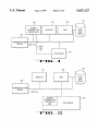
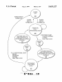
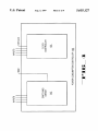
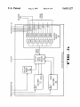
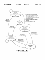
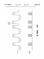
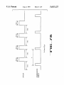
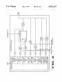
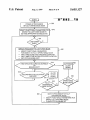
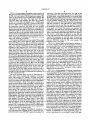
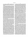
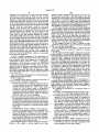
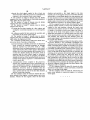
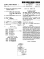
USOO5655 127A
United States Patent [19]
[11] Patent Number:
[45] Date of Patent:
Rabe et al.
[54]
METHOD AND APPARATUS FOR CONTROL
OF POWER CONSUIVIPTION IN A
0419908
0451661
COMPUTER SYSTEM
5,655,127
Aug. 5, 1997
6/1990 European Pat. 0ft. .
3/1991 European Pat. O?'. .
(List continued on next page.)
[75] Inventors: Jeifrey L. Rabe. Rancho Cordova;
OTHER PUBLICATIONS
Zohar Bogin. Folsom; Ajay V. Bhatt,
_
“
~
.
_
El Dorado Hills; James R Kardach’
Slater, Michael, MIPS Prevzews 64-bit R4000 Archztec
San Jose; Nilesh V_ Shah’ Folsom’ all
of can.
ture , Microprocessor Report, vol. 5, Issue: n2, p1(6), Feb.
6’ 1991'
Case, Brian. “R4000 Extends R3000 Architecture With
[73] Assignee: Intel Corporation, Santa Clara, Calif,
64-bit Capabilities”, Microprocessor Report, vol.: v5, Issue:
n19, p10(4), Oct. 16, 1991.
2
l. N .:
Wilson ~ Ron ’ “MIPS Rethinks RISC With SuP e'PP
i elining” ’
67
[ 1] App 0 612’ 3
[22] Filed:
Mar. 8, 1996
Computer Design. V01: V30, Issue: n3, p28(3), Feb. 1, 1991.
Intel Automotive Components Handbook, “Power-On
Reset”, 1988, pp. 10-24 & 10-25.
Motorola MC6802032—Bit Microprocessor User’s Manual,
Related US. Application Data
3rd Edition, 1990,
. 1-3.
[63]
[51]
Continuation of Ser. No. 191,651, Feb. 4, 1994, abandoned.
Int Cl 6
G06F 1,26
Pp
Primary Examiner—-Glenn A. Auve
[52]
US. Cl.
o ..................
-----------------------------------------------------.. 395l750.04; 345/838;
u
Attorney’ Agent) or Firm_B1ake1y,
K.
sokolo?-‘q Taylor &
[58]
Field of Search ................................... .. 395/750, 838,
Zafman
,
[56]
A computer system having a responsive low-power mode
References Clted
U_S_ PATENT DOCUMENTS
and a full-power mode of operation. The computer system
includes a power consumption controller, a processor and a
communication device. The power consumption controller
3,623,017 11/1971 Lowell et a1. .
generates an interrupt signal in response to a low power
3,715,729
2/ 1973 Mercy;
3,736,569
5/1973 130111161115 61111- -
event or a fully operational event. The power consumption
3,737,637
6/1973 Frankeny et a1.
395/750
controller also generates a clock control signal. The clock
371/28
Conn-o1 signal is deassm-tcd during the fu]l_p0we1- mode of
3,395,311 7/1975 Bass? et 31- ~
3’919’695 11/1975 G°°dmg '
4’077’016
game; ct ala'l'
2/1978 82:56 2: a1‘ '
4:095:267
6,1978 Modmoto _ ' '
operation and alternatively asserted for a ?rst duration and
deasserted for a second duration during the low-power mode
of operation. In response to an asserted clock control signal,
the processor suppresses the internal clock signal to at least
one functional block within the processor and in response to
a deasserted clock control signal, the processor transmits the
internal clock signal to at least one functional block within
(List continued on next page.)
the processor. By transmitting the internal clock signal to at
least one functional block within the processor during the
low-power mode of operation, the processor may respond to
cormnunication signals from a communication device dur
FOREIGN PATENT DOCUMENTS
0103755
0140814
8/1983
5/1984
0242010 12/1987
0368144 2/1989
0366250 9/1989
European Pat.
European Pat.
European Pat.
European Pat.
European Pat.
Otf.
O?'.
O?‘.
O?’.
O?'.
.
.
.
.
.
ing the low-power mode of operation.
18 Claims, 9 Drawing Sheets
POWENUP mocrssoi
m
lNNLLYOPERATlONALN?DE
srirci runcnurut PARAMETERS | on
SWll‘Qi YD LOW vowen \WCE Ev
serum; umurnm: ENABLE 5H5
on
LCW
zvrw
v
FA'l
1 not».
- mPuv um stoma Flnsr SPEClFlED non/mm
- mPurmn stun: srcom SFEClF ED rumor»:
rum spa-mm nmwlon rxrlazu'l
on
WEAK EVENI?
Y
5,655,127
Page 2
[LS RAJ'ENT DOCUMENTS
5,077,686 12/1991 Rubinstein.
5,083,266
1/1992 w616n6b6 .............................. .. 395/275
5,103,114
5,123,107
4/1992 1311611.
6/1992 Mensch, I12.
5,129,091
5,133,064
7/1992 Y611m616 6161..
7/1992 1161166161..
4,365,290 12/1982 Nelms et a1. 1
5,151,992
9/1992 Nagae,
4,405,898
5,167,024 11/1992 Smith 6161. .......................... .. 395/375
4,203,153
4,264,863
5/1980 Boyd4/1981 K9Jm_1_a-
4,293,927 10/1981 Hoshu4,300,019 11/1981 Toyomaki9/1983 Flemming-
4,479,191 10/1984 N6jim6 6161..
4,545,030 10/1985 Kitchin4,615,005 9/1986 Maejima 9t a1~4,638,452 1/1987 Schultz et 61..
4,639,864 1/1987 Katzman et a1-4,667,289 5/1987 Yoshida 9141-.
4,669,099 5/1987 Zinn.
4,698,748 10/1987 Juzswik 6161..
4,758,945 7/1988 Remedi4,763,294
8/1988 F9119
5,175,845 1271992 11616.
5,189,647 2/1993 Suzuki 6161,.
5,220,672 6/1993 N6k66 6161..
5,239,652 3/1993 $611,611 6161..
5,249,298 9/1993 B01311 6: 61..
5,251,320 10/1993 Kuzawinski 6161..
5,263,028 11/1993 Borgnjs et 211..
5,319,771 6/1994 Takeda,
5,329,621 7/1994 Burgess 6161..
5,335,168
8/1994 w61k6r .................................. .. 364/707
4,766,597 8/1988 K616.
4,780,843 10/1988 Tietjen.
4,814,591 3/1989 Nara e1 41--
5,336,939 8/1994 Eitrheim 6161..
5,355,501 10/1994 616666161.
5,359,232 10/1994 Eitrheim 6161..
4,823,292
4/1989 H?lwn-
4,841,440
611989 Yonezu et a1--
5,369,771
5,396,635
4,881,205 11/1989 Aih6r6.
4,896,260 1/1990 Hyatt4,907,183 3/1990 Tanaka4,922,450 5/1990 126666161.
4,935,863 6/1990 Calvas er a1~~
4,979,097 12/1990 Trioloet 61..
11/1994
................... .. 395/750
3/1995 Fung ..................................... .. 395/800
5,404,546 4/1995 s16w6n.
5,428,754 6/1995 Baldwin.
5,461,652 10/1995 HOngO.
FOREIGN PATENT DOCUMENTS
4,980,836 12/1990 (2611616161. .......................... .. 364/483
0478132 12/1991
4,983,966
4,991,129
5,021,679
0654726 10/1994 1361616666 Pal. 011..
9302408 2/1993 Germany,
2010551 11/1978 United Kingdom,
1/1991 Groneet 61..
2/1991 SWal‘lZ.
6/1991 Fairbanks 6t 61..
5,059,924 10/1991 Check.
1316616666 Pat. 011..
2130765 10/1983 United Kingdom.
US. Patent
Aug. 5, 1997
105
1
‘
POwER
CONSUMPTION
CONTROLLER
Sheet 1 of 9
5,655,127
104
102
/
”
MONITOR
RAM
101
.
1/06
COMMUNICATIONS
\
DEV'CE
BUS 125
3
SMI#
/LINE
151
103
PROCESSOR
PIE
/
1
104
102
/
/
MONITOR
RAM
1/06
COMMUNICATIONS
DEVICE
\
BUS 125
POWER
/103
CONSUMPTION
CONT1%€LLER
PROCESSOR
US. Patent
Aug. 5, 1997
Sheet 2 Of 9
5,655,127
POWER
OFF
POWER SWITCH
5—34
TURNED OFF
POWER I l POWER
SWITCH
TURNED OFF
SWITCH
TURNED ON
POWER ON
FULLY
OPERATIONAL MODE
.522
LOW POWER EVENT
COUNTER EXPIRES
EXTSMI#
REAL TIME CLOCK
RUN SMM HANDLER
HARD DISK SPUN UP
CRT SCREEN AT NORMAL
INTENSITY
ASSERT
SMI#
29.
51E
RUN SMM HANDLER
HARD DISK SPUN DOWN
ORT SCREEN OFF OR AT LOW
INTENSITY
FULLY OPERATIONAL EvENT
MOUSE
KEYBOARD
EXTSMI#
§_2_g_
REAL TIME CLOCK
RESPONSIVE
LOW POWER
MODE
E
PIH__3
US. Patent
Aug. 5, 1997
Sheet 3 of 9
$21%5
23E%;:
6@2058 8$56%28
a.%.
5,655,127
$52m0:32985
iWlH-MI
US. Patent
Aug. 5, 1997
Sheet 4 0f 9
5,655,127
.IOm
m9
EmwofmO2gE9owm
3 9th
520.65% % §
E5ajo2zO
g
51M2502
éa95z:gw Mm:25mum
Em a
159E: mm
mmw
vmw
min-HF!
US. Patent
Aug. 5, 1997
Sheet 5 Of 9
5,655,127
STPCLK#
DEAssERTED
(FULLY OPERAT'ONAL MODE)
— LOW TIMER REGISTER LOADED
WITH FIRsT SPECIFIED DuRATION
E
- LOW TIMER REsET
— HIGH TIMER REGISTER LOADED
WITH SECOND SPECIFIED DURATION
_ HIGH TIMER REsET
STPCLK#
— DESIRED BREAK EvENT ENABLE
ENABLE BIT
BITs SET
cLEARED
- STPCLK# ENABLE BIT SET
EXPIRATION
OF HIGH TIMER
5TPCLK#
AssERTED
‘
(RESPONSIVE
LOW POWER MODE)
BREAK SIGNAL
EXPIRATION
(BREAK EVENT
WITH BIT ENABLED)
OF LOW TIMER
STPCLK#
DEAssERTED
(RESPONSIVE
LOW POWER MODE)
E4.
BREAK SIGNAL
(BREAK EvENT
WITH BIT ENABLED)
HIGH TIMER
RESET
L63.
FII3_E
US. Patent
Aug. 5, 1997
mm‘
mm“
mm"
“3
“2
“m3.
ima 5%
mm
m3.
17
mmm1
Sheet 6 0f 9
5,655,127
US. Patent
Aug. 5, 1997
Sheet 7 of 9
5,655,127
mew
mmm:
mew
w1m+EAx
mew
mmm1
wfoncw
29530 @206
.mlhui
US. Patent
Aug. 5, 1997
5,655,127
Sheet 9 Of 9
FIE_EI
@
POWER UP PROCESSOR
IN FULLY OPERATIONAL MODE
/ 939
I
SELECT FUNCTIONAL PARAMETERS FOR / 940
SWITCH TO LOw POWER MODE BY
SETTING APPROPRIATE ENABLE BITS
941
LOW POWER
EVENT
SWITCH PROCESSOR TO LOW POWER MODE
MODIFY FUNCTIONAL PARAMETERS
FOR SWITCH TO FULLY OPERATIONAL MODE
INPUT AND STORE FIRST SPECIFIED DURATION
INPUT AND STORE SECOND SPECIFIED DURATION
SET STPCLK# ENABLE BIT
V
944
FIRST SPECIFIED DURATION EXPIRED?
OR
BREAK EVENT?
946
N
SECOND SPECIFIED DURATION
EXPIRED?
N
SUPPRESS
CLOCK
SIGNAL
ALLOW
CLOCK
947 /
OPERATIONAL
MODE EVENT?
FULLY
OPERATIONAL
MODE EVENT?
SWITCH PROCESSOR TO FULLY
OPERATIONAL MODE
—— MODIFY FUNCTIONAL PARAMETERS FOR
SWITCH TO LOW POWER MODE
— CLEAR STPCLK# ENABLE BIT
I
5,655,127
1
2
METHOD AND APPARATUS FOR CONTROL
OF POWER CONSUMPTION IN A
COMPUTER SYSTEM
for switching the computer system between a fully opera
tional mode and a responsive low power mode. In addition,
in one embodiment the power consumption controller can
include a clock controller for cyclically suppressing a clock
signal to a portion of a processor for a ?rst speci?ed duration
This is a continuation of application Ser. No. 08/ 191,65 1,
?led Feb. 4. 1994, now abandoned.
FIELD OF THE INVENTION
when the computer system is in the responsive low power
The present invention relates to the ?eld of computer
systems. More particularly, the present invention relates to
the control of power consumption in computer systems.
10
BACKGROUND OF THE INVENTION
include a break event device for signaling the clock con
troller to allow the clock signal to be transmitted to the
portion of the processor for a second speci?ed duration.
Finally, the power consumption controller can include a
Existing computer systems consume large amounts of
electrical power when operating in the fully operational
mode. These systems typically lack power consumption
controllers and thus when left idle. the systems continue to
remain in the fully operational mode. The United States
Environmental Protection Agency (EPA) has established
guidelines encouraging the manufacture of computer sys
tems which when left idle for an extended period only
selection device for selecting functional parameters of the
power consumption controller, which de?nes events causing
switching between the modes.
BRIEF DESCRIPTION OF THE DRAWINGS
consume a speci?ed amount of electrical power or less.
One prior power consumption controller was used in
portable computer systems. The prior controller would turn
off the monitor. spin down the hard disk and shut down the
central processing unit (CPU). Because the prior controller
mode. Under this embodiment, the clock controller also
cyclically allows the clock signal to be transmitted to the
portion of the processor for a second speci?ed duration
when the computer system is in the responsive low power
mode. Moreover, the power consumption controller can
25
shut down the CPU, the portable system could not be
responsive to signals coming from a communications
device. for instance, a network, fax machine or modern.
The present invention is illustrated by way of example,
and not by way of limitation, in the ?gures of the accom
panying drawings and in which like reference numerals refer
to similar elements and in which:
FIG. 1 is a block diagram illustrating a computer system
of one embodiment of the present invention.
FIG. 2 is a block diagram illustrating a computer system
with a processor incorporating the power consumption con
troller.
FIG. 3 is a state diagram illustrating the operation of a
However. most portable systems were not connected to a
communications device anyway and thus did not need to be
responsive to signals from the communications device.
Desktop computer systems on the other hand, usually are
power consumption controller of FIG. 1.
connected to a communications device and need to be
FIG. 4 is a block diagram illustrating the power consump
tion controller of FIG. 1.
of the prior controller in a desktop system connected to a 35
FIG. 5 is a block diagram illustrating a clock controller of
communications device causes the desktop system to fail to
FIG.
4.
respond to signals from the communications device after a
FIG. 6 is a state diagram illustrating the operation of
speci?ed idle period when the CPU is shut down. With the
STPCLK# signal state machine of FIG. 5.
network as a communications device. the network deacti
responsive to signals from the communications device. Use
vates the system address, in effect. removing the system
from the network after the failure to respond. Other systems
40
FIG. 7a is a timing diagram illustrating the operation of
a clock controller of FIG. 5.
in the network becomes unable to communicate with the
FIG. 7b is a timing diagram illustrating communication
signals being transmitted from a communication device.
FIG. 8 is a block diagram illustrating a switching device
desktop system and the desktop system becomes unable to
receive any information from the network.
Similarly, with a fax machine or modern as the commu 45 of a seventh embodiment of the present invention.
nications device connected to the desktop system.v the prior
controller in the desktop system causes the desktop system
FIG. 9 is a flow chart illustrating the steps for controlling
the power consumption of a processor.
to fail to respond to communications signals. In this case. the
fax machine or modern ceases transmission of data and the
desktop system fails to receive the data.
It would be highly bene?cial to have a desktop computer
system with a power consumption controller that switches
the system between a fully operational mode and a respon
sive low power mode, where the responsive low power
mode still allows the system to be responsive to communi
cations device signals. The system could then satisfy EPA
guidelines by switching to the responsive low power mode
after a speci?ed idle period, and respond to communications
signals or process information from the communications
device.
Thus, what is needed is a power consumption controller
that switches a computer system between a fully operational
mode and a responsive low power mode.
DETAILED DESCRIPTION
50
A power consumption controller and a method for con
trolling power consumption is described. In the following
description, the invention is described with reference to
speci?c exemplary embodiments thereof. It will, however,
55
be evident that various modi?cations and changes may be
made thereto without departing from the broader spirit and
scope of the invention as set forth in the appended claims.
The speci?cations and drawings are, accordingly, to be
regarded in an illustrative rather than a restrictive sense.
FIG. 1 is a block diagram illustrating a computer system
of one embodiment of the present invention. The computer
system includes hard disk drive 101, random access memory
(RAM) 102, processor 103, monitor 104, power consump
tion controller 105 and communications device 106. Hard
SUMMARY OF THE INVENTION
65 disk drive 101 and monitor 104 are coupled to processor 103
A novel power consumption controller is described. The
by bus 125. Processor 103 in turn is coupled to power
power consumption controller comprises a switching device
consumption controller 105 by line 151. It will be appreci
5,655,127
3
4
ated that power consumption controller 105 can be incor
?ed duration are set such that processor 103 can acknowl
porated into other devices.
FIG. 2 is a block diagram illustrating a computer system
edge within the latency period.
with a processor incorporating the power consumption con
troller. In the system. power consumption controller 105 is
built into processor 103. Processor 103 has the necessary
circuitry and logic to carry out the functions of power
sive low power mode until the power switch is turned off or
a fully operational event occurs. When power switch is
turned oif, controller 105 transitions to the power oif state
Power consumption controller 105 remains in the respon
where controller 105 along with the rest of the system is
turned 01?, state 534. On the other hand, when a fully
consumption controller 105. In addition, signals from power
consumption controller 105 that would normally transmitted
operational event occurs, controller 105 asserts a second
SMI# signal, state 538. Fully operational events are events
which cause the switch to the fully operational mode and
like low power events are selectable by processor 103. Fully
across line 151 to processor 103 now proceed directly to
processor 103.
FIG. 3 is a state diagram illustrating the operation of a
power consumption controller of FIG. 1. When the system
operational events can include movement of a mouse device,
is ?rst turned on, the system transitions from the power off
state 534 to the power on state 535 where the system is in
input to a keyboard, the receipt of an external signal from a
push button (EXTSMI#), and a signal from a real time clock
the fully operational mode. Power consumption controller
device indicating current time is the preset time for switch
105 remains in the fully operational mode until the power
ing to fully operational mode. It will be appreciated that
switch is turned off or a low power event occurs. When
other events can also be selected as fully operational events.
power switch is turned off, controller 105 transitions to the
power off state where controller 105 along with the rest of
the system is turned oif. On the other hand, when the power
switch is not turned oif. power consumption controller 105
As described above, controller 105 responds to a fully
operational event by asserting a second SMI# signal to
processor 103, state 538. Processor 103 responds by running
the SMM Handler software, state 529. SMM Handler
includes code that processor 103 executes to instruct the
Waits for a low power event Low power events are events
hard disk to spin up and the monitor to turn on to normal
which cause the switch to the responsive low power mode
and are selectable at boot up of the system or by processor 25 intensity. Processor 103 then executes SMM Handler code to
switch to the fully operational mode, state 535. In the fully
103. Low power events can include the expiration of elapsed
operational mode, controller 105 no longer asserts the STP
time as indicated by a counter, the receipt of an external
CLK# signal and processor 103 remains fully operational.
signal from a push button (EXTSMI#), and a signal from a
Controller 105 operates in the fully operational mode as
real time clock device indicating current time is the preset
described above.
time for switching to responsive low power mode. It will be
appreciated that other events can also be selected as low
FIG. 4 is a block diagram illustrating the power consump
tion controller of FIG. 1. Power consumption controller 105
power events.
Power consumption controller 105 responds to a low
power event by asserting a SMI# signal to processor 103,
state 536. Processor 103 responds by running software
includes switching device 612 and clock controller 611.
Switching device 612 is coupled to inputs from processor
35
mode button, real time clock or other similar devices. In
addition, processor 103 also has inputs to clock controller
611. Switching device 612 switches the computer system
between a fully operational mode and a responsive low
power mode by asserting a SMI# signal. As described above,
when the computer system is in the fully operational mode,
an assertion of a SMI# signal switches the computer system
to a responsive low power mode. On the other hand, when
speci?ed duration and deasserts STPCLK# signal to proces
sor 103 for a second speci?ed duration. While controller 105
remains in the responsive low power mode, it repeats the
assertion and deassertion of STPCLK# signal in the manner
described above. Processor 103 responds to the assertion of
STPCLK# signal by suppressing the clock signal to a
portion or all of processor 103. Processor 103 responds to
the deassertion of STPCLK# signal by recoupling the clock
45
50
signal to the previously suppressed portion of processor 103.
It will be appreciated that processor 103 is at least partially
off for the ?rst speci?ed duration while STPCLK# signal is
asserted and operating at full capacity for the second speci
?ed duration while STPCLK# signal is deasserted. Because
processor 103 is at least partially off for the ?rst speci?ed
duration in each cycle, power consumption is reduced. In
addition, because processor 103 is operating at full capacity
for the second speci?ed duration in each cycle, processor
103 is responsive to signals from communications device
103 and other devices in the computer system. The other
devices can include a mouse device, keyboard. low power
called SMM Handler as shown in state 528. SMM Handler
includes code that processor 103 executes to instruct the
hard disk to spin down and the monitor to turn off or reduce
intensity. Processor 103 then executes the SMM Handler
code to switch to the responsive low power mode, state 537 .
In the responsive low power mode, controller 105 asserts an
active low STPCLK# signal to processor 103 for a ?rst
the computer system is in the responsive low power mode,
an assertion of a SMI# signal switches the computer system
to a fully operational mode.
In this embodiment, switching device 612 asserts the
SMI# signal to processor 103 using line 151. However,
under an alternative embodiment, switching device 612 can
also assert the SMI# signal to processor 103, clock controller
611 or to other devices in the computer system such as
monitor 104 or hard disk drive 101. In addition, switching
device 612 can assert the SMI# signal on bus 125 to a
55
separate device which asserts another SMI# signal directly
to processor 103 on a dedicated line. When processor 103
receives the SMI# signal, it signals clock controller 611 to
switch it to a responsive low power mode if it was previ
ously in a fully operational mode; it signals clock controller
611 to switch it to a fully operational mode if it was
106 during the second speci?ed duration. Thus, it will be
appreciated that processor 103 will be su?iciently respon
previously in a responsive low power mode.'As described
above, in the responsive low power mode, clock controller
sive to remain on a network where the time between each
611 asserts STPCLK# signal to processor 103 for a ?rst
network poll is greater than the ?rst speci?ed duration plus
the second speci?ed duration. It will also be appreciated that
speci?ed duration and deasserts STPCLK# signal to proces
processor 103 will be su?iciently responsive to remain on a
sor 103 for a second speci?ed duration. In the fully opera
tional mode, clock controller 611 no longer asserts STP
network where the ?rst speci?ed duration and second speci
CLK# signal and processor 103 remains fully operational.
65
5,655,127
5
6
FIG. 5 is a block diagram illustrating a clock controller of
transitions to the fully operational mode. state 760. In this
state, STPCLK# is deasserted. When processor 103 receives
an SMI# signal. it runs SMM Handler. In executing SMM
Handler, processor 103 loads the low timer register with the
FIG. 4. Clock controller 611 comprises of STPCLK# enable
bit 753, low timer register 752 and high timer register 754
which are all coupled to processor 103. Clock controller 611
also comprises of low timer 713. high timer 715 and
STPCLK# signal state machine 714. When the computer
system is in the fully operational mode, a SMI# signal
asserted by switching device 612 to processor 103 causes
processor 103 to run the SMM Handler code. In executing
the instructions, processor 103 loads the ?rst speci?ed
duration into low timer register 752 and the second speci?ed
duration into high timer register 754. Processor 103 then sets
STPCLK# enable bit. In this embodiment, the ?rst speci?ed
duration and the second speci?ed duration range from 32
microseconds to eight milliseconds in 32 microsecond incre
?rst speci?ed duration and loads high timer register with the
second speci?ed duration, sets the desired break event
10
enable bits and sets the STPCLK# enable bit. State machine
714 then transitions to state 762 with low timer and high
timer already reset. In state 762, state machine 714 asserts
the STPCLK# signal. When state machine 714 receives a
break signal or low timer 713 expires, state machine 714
transitions to state 763 where state machine 763 resets high
timer 715. Then state machine 714 transitions to state 764
where it deasserts the STPCLK# signal. When state machine
714 receives a break signal, it transitions to state 763 and
ments. It is to be appreciated that clock controller 611 can
resets high timer 715. When high timer 715 expires, state
utilize other ranges by utilizing other high timers and low
timers with different clock pulses.
When processor 103 loads low timer register 752 and high
timer register 754, it resets both low timer 713 and high
machine 714 transitions to state 761 where it resets low
timer 713 and transitions to state 762. When processor 103
deasserts STPCLK# enable bit 753, state machine 714
transitions back to state 760.
timer 715. When processor 103 sets STPCLK# enable bit
753. STPCLK# signal state machine 714 asserts STPCLK#
signal. The setting of STPCLK# enable bit 753 marks the
beginning of the responsive low power mode. STPCLK#
signal state machine 714 continues to assert the STPCLK#
FIG. 7a is a timing diagram illustrating the operation of
the clock controller of FIG. 5. In the responsive low power
mode as described above. clock controller 611 asserts active
25
signal until low timer 713 signals the end of the ?rst
speci?ed duration. When low timer 713 expires. STPCLK#
signal state machine 714 resets high timer 715 and deasserts
the STPCLK# signal until high timer 715 signals the end of
the second speci?ed duration. When high timer 715 expires,
STPCLK# signal state machine 714 resets low timer 713 and
asserts STPCLK# until low timer 713 expires. The cycle
continues until switching device 612 asserts a SMI# signal
to processor 103 causing processor 103 to run the SMM
Handler code. In executing the instructions, processor 103
35
clears STPCLK# enable bit 753 which in turn causes the
STPCLK# signal state machine 714 to deassert the STP
CLK# signal. STPCLK# signal remains deasserted until a
subsequent switch to the responsive low power mode. The
clearing of STPCLK# enable bit 753 marks the beginning of
the fully operational mode.
The cycle described above can also be interrupted by a
break event. Clock controller 611 comprises of selection
device 730 coupled to a plurality of break event lines.
Selection device 730 in turn comprises of AND gate 731 and
break event enable bits 732 coupled to processor 103. When
a break event occurs, a break event signal is asserted on a
break event line. Break events can include a network signal
that the processor must service immediately or other opera
low STPCLK# signal for a ?rst speci?ed duration and
deasserts STPCLK# signal for a second speci?ed duration.
In this example. the ?rst speci?ed duration is eight milli
seconds and the second speci?ed duration is 32 microsec
onds. When STPCLK# is asserted, internal processor CLK
is suppressed and when STPCLK# is deasserted, internal
processor CLK is transmitted. Clock controller 611 also has
circuitry allowing it to respond to break events. When a
break event occurs as shown in FIG. 8, STPCLK# signal is
deasserted for the second speci?ed duration of 32 micro
seconds. Afterwards, STPCLK# signal is asserted for the
?rst speci?ed duration of eight milliseconds. It will be
appreciated that the break event only affects the ?rst speci
?ed duration of one cycle. Subsequent cycles ' continue
40
unaffected by the break event.
FIG. 7b is a timing diagram illustrating communication
signals being transmitted from a communication device.
According to FIG. 7b, the interval between two consecutive
communication signals has a duration greater than the sum
of the ?rst time duration and the second time duration of the
STPCLK#. This ensures that one of the communication
45
signals will be received while the STPCLK# is deasserted.
The assertion of a STPCLK# signal as described above
suppresses the internal clock to portions of processor 103
because processor 103 has circuitry which enables the
suppression. In one embodiment, processor 103 includes a
tions which require immediate processor activity. When a 50 plurality of functional blocks each performing a speci?ed
break event signal is asserted, AND gate 731 generates a
function in processor 103. Each functional block has a clock
break signal if the associated enable bit 732 is set. Thus,
input coupled to an AND gate with two inputs to the gate.
processor 103 can select the break events that generate a
break signal by selectively setting the associated enable bits
One input is coupled to the internal clock signal and the
second input is coupled to the output of a NAND gate. Each
732. Processor 103 carries out the selection by utilizing the 55 NAND gate also has two inputs. One coupled to an inverted
SMM Handler code which it runs prior to the assertion and
STPCLK# input line and the second coupled to a line
deassertion of STPCLK# signal. When STPCLK# signal
connected to either a high or low voltage potential. The line
state machine 714 receives a break signal. it resets high
is connected during the manufacture of processor 103 and
timer 715 and deasserts STPCLK# signal for the second
determines whether clock suppression is enabled for that
speci?ed duration. It will be appreciated that a break event
functional block. It will be appreciated that when the line is
with the enable bit set causes STPCLK# signal state
connected to a high voltage potential, clock suppression will
machine 714 to immediately deassert the STPCLK# signal
never occur in that particular functional block. On the other
for the second speci?ed duration when clock controller 611
hand, when the line is connected to a low voltage potential,
is in the responsive low power mode.
clock suppression will occur when STPCLK# signal is
FIG. 6 is a state diagram illustrating the operation of
asserted. In this manner, portions of processor 103 can be
STPCLK# signal state machine of FIG. 5. When the com
selected at manufacture for clock suppression. Under yet
puter system powers up. STPCLK# signal state machine 714
another embodiment, the second input of each NAND gate
5,655,127
7
8
can be coupled to an enable bit. The enable bits act as a
cessor 103 or another device can set counter enable bit 917 ,
selection mechanism allowing processor 103 or other device
to select and modify the particular functional block for clock
mouse counter reset enable bit 918, keyboard counter reset
suppression.
enable bit 921. Processor 103 or the other device can clear
mouse power on enable bit 927 and keyboard power on
enable bit 926. With this set of functional parameters,
enable bit 919, real time clock enable bit 920, and button
FIG. 8 is a block diagram illustrating a switching device
of a seventh embodiment of the present invention. Switching
device 612 includes counter 92A and selection device 916.
counter 924 is activated and the SMI# signal when generated
Counter device 924 is activated when the computer system
is powered up and begins counting elapsed time. Because
the computer system powers up in the fully operational
mode, the elapsed time maintained by counter device 924 is
the elapsed time since the start of the fully operational mode.
is transmitted to processor 103. In addition, mouse move
ment and keyboard input while the system is in the fully
10
Counter device 924 includes a register for storing a preas
signed value representing a speci?ed elapsed time. Counter
device 924 also includes a comparator for comparing the
preassigned value to the elapsed time. When the elapsed
time equals the preassigned value, an active low signal is
generated which becomes the SMI# signal. Counter device
15
operational mode will reset counter 924 because bits 918
and 919 are set. Moreover, the real time clock device can
generate a SMI# signal that is transmitted to processor 103.
Furthermore, the computer system can include an external
button which when pressed generates an active low
EXTSMI# signal. When the EXTSM1# signal is asserted, an
SMI# signal is also asserted because bit 921 is set. It is to be
appreciated that the assertion of a SMI# signal causes the
computer system to transition to the responsive low power
924 has a reload input coupled to the mouse device, and
keyboard. When a signal is transmitted from either of the
mode. Mouse movement and keyboard input do not generate
a SMI# signal because bits 927 and 926 are cleared.
mouse device or keyboard, the counter is reset and starts
Before the system transitions to the responsive low power
counting the elapsed time from initial value. The counter is
mode, processor 103 or another device can clear counter
enable bit 917, mouse counter reset enable bit 918. and
register with the preassigned value prior to the beginning of
keyboard counter reset enable bit 919. Processor 103 or the
the fully operational mode. Thus. at the initiation of the fully
operational mode, counter 92A is reset. Counter 92A is also 25 other device can set mouse power on enable bit 927,
reset when an input to the keyboard is made or when mouse
keyboard power on enable bit 926, real time clock enable bit
movement is detected. In this manner, counter 92A measures
920, and button enable bit 921. With this set of functional
also reset to initial value when processor 103 loads the
the elapsed time between the last mode switch or keyboard
parameters, counter 924 is deactivated. Mouse movement,
input or mouse movement and asserts a SMI# signal when
keyboard input and the pressing of the EXTSM1# button will
the elapsed time equals a preassigned value. In this manner,
generate a SMI# signal. The real time clock device can also
generate a SMI# signal that will be transmitted to processor
103. The SMI# signal causes the computer system to tran
sition back to the fully operational mode as described above.
human interface through a keyboard or mouse reloads the
counter which ensures that processor 103 is fully active and
operative during such use.
Under other embodiments. switching device 612 also
The speci?ed real time can be changed in the responsive low
includes a real time clock device. The real time clock device 35 power mode and in the fully operational mode. The real time
has a register for storing a preassigned value representing a
clock device can include an input coupled to processor 103
speci?ed real time. In addition, the real time clock device
or other device which allow them to change the preassigned
has a comparator for comparing the preassigned value to the
value representing the speci?ed real time in the real time
input provided by the real time clock. When the real time as
clock device. Thus, a ?rst real time can be assigned in the
indicated by the real time clock equals the preassigned
fully operational mode to transition the system to the respon
value, an active low SMI# signal is asserted. In this manner,
sive low power mode at the ?rst real time and a second real
the real time clock device asserts a SMI# signal to switch
time can be assigned in the responsive low power mode to
modes when real time has reached a preassigned value.
transition the system to the fully operational mode at the
Under this embodiment though, the real time clock device is
second real time.
external to switching device 612 and transmits the active 45
FIG. 9 is a ?ow chart illustrating the steps for controlling
SMI# signal as an input to switching device 612.
the power consumption of a processor. When the processor
Finally, switching device 612 includes selection device
916. Selection device 916 includes a plurality of enable bits.
The enable bits allows the functional parameters of the
power consumption controller to be selected and modi?ed
Selection device 916 is coupled to an input line from which
the enable bits can be set or cleared by processor 103 or
other devices. Each of the enable bits is coupled to an AND
is ?rst powered up, it transitions to the fully operational
mode, block 939. Next, the processor selects the functional
parameters which de?ne events causing a switch to the
50
responsive low power mode, block 940. The functional
parameters are selected by selling and clearing the appro
priate enable bits. The processor remains in the fully opera
tional mode until a low power event occurs as shown by
gate 922 located between the associated device (i.e., mouse,
block 941. Low power events are de?ned by the functional
keyboard, real time clock device, EXTSMIii) and the SMI# 55 parameters selected by the processor. Low power events can
signal output. Thus, when a particular enable bit is set, SMI#
include a signal at a speci?ed time to switch to a responsive
signals generated by the associated device is transmitted to
low power mode, a signal from an external button device to
processor 103. On the other hand, when a particular enable
switch to a responsive low power mode, and the expiration
bit is cleared, SMI# signals generated by the associated
of a speci?ed elapsed time as indicated by a counter. The
device is suppressed. In this example, selection device 916
counter can be reset upon an occurrence of a speci?ed event,
includes counter enable bit 917, mouse counter reset enable
i.e., mouse movement or keyboard input. When a low power
event occurs, the processor is switched to the responsive low
power mode as shown in block 942. Functional parameters
are modi?ed in order to de?ne events causing a switch to the
bit 918. keyboard counter reset enable bit 919, real time
clock enable bit 920, button enable bit 921, mouse power on
enable bit 927 and keyboard power on enable bit 926. Other
enable bits representing other events can also be included. 65 fully operational mode. In addition, the ?rst speci?ed dura
tion and the second speci?ed duration is inputted and stored.
When the computer system powers up, it transitions to the
The STPCLK# enable bit is also set marking the start of the
fully operational mode. In the fully operational mode, pro
5,655,127
9
10
responsive low power mode. As long as the ?rst speci?ed
machine, further wherein the ?rst register stores the ?rst
time duration and provides a ?rst input signal to the state
machine, the second register stores the second time duration
and provides a second input signal to the state machine, the
state machine receives an enable signal and alternatively
generates an asserted clock control signal for the ?rst time
duration and a deasserted clock control signal for the second
duration has not expired and no break event has occurred,
the clock signal to the selected portions of the processor is
suppressed. blocks 944 and 945. When the ?rst speci?ed
duration has expired or a break event occurs, the clock signal
to the selected portions of the processor is allowed as long
as the second speci?ed duration has not expired. blocks 946
and 947. When the clock signal is allowed to the select
portions of the processor, the processor can respond to
communications device signals. block 947. When the second
speci?ed duration has expired, the clock signal to the
selected portions of the processor is suppressed until a break
event occurs or the ?rst speci?ed duration has expired,
blocks 944 and 945. In the above steps, after the clock signal
has been suppressed or has been allowed a fully operational
mode event will switch the processor to the fully operational
mode, blocks 948. 949 and 950. On the other hand. when a
fully operational mode event does not occur, the ?rst speci
5
time duration in response to an asserted enable signal.
3. The computer system of claim 2. wherein the controller
further includes a break event selection device coupled to
the state machine, the break event selection device including
at least one break event input that is capable of receiving the
break event signal, when at least one of the break event
inputs receive a break event signal that corresponds to a
selected break event, the break event selection device pro
15 vides a third input signal to the state machine, and the state
machine causes the clock control signal to be immediately
deasserted for at least the second time duration.
4. The computer system of claim 1, wherein the fully
?ed duration or the second speci?ed duration continues as
operational event includes a mouse movement, a keyboard
applicable. blocks 948. 946. 949 and 944. Before the pro 20 entry, or a real-time clock signal.
cessor has been switched to the fully operational mode, the
functional parameters which de?ne events causing the
switch to the responsive low power mode are modi?ed. The
5. The computer system of claim 1, wherein the low
power event includes a count-down signal or a real-time
clock signal.
6. The computer system of claim 1, wherein the controller
processor returns to block 941 and continues in a loop until
the processor is turned off.
25 further includes a low power/fully operational event selec
tion device having at least one low power/fully operational
In order to facilitate explanation of the embodiments of
the present invention, the responsive low power mode has
been described with clock suppression occurring ?rst
(STPCLK# asserted). However, under an alternative
embodiment, clock allowance occurs ?rst (STPCLK#
deasserted) in the responsive low power mode. It will be
appreciated that the alternative embodiment may be imple
mented merely by adjusting state machine 714 so that
STPCLK# is deasserted ?rst until the expiration of high
timer 715 and then SI‘PCLK# is asserted until the expiration
event input that is capable of receiving a low power event
signal or a fully operational event signal, when the low
power/fully operational event selection device receives the
low power event signal that corresponds to a selected low
power event while in the full-power mode of operation, the
35
of low timer 713.
operation, the switching device generates the interrupt signal
Thus, a novel method and apparatus for controlling power
consumption has been described.
What is claimed is:
1. A computer system having a full-power mode and a
switching device generates the interrupt signal to transition
the computer system from the full-power mode to the
low-power mode of operation, and when the low power
event/fully operational event selection device receives the
fully operational event signal that corresponds to a selected
fully operational event while in the low-power mode of
40
low-power mode of operation comprising:
to transition the computer system from the low-power mode
to the full-power mode of operation.
7. A method for controlling the power consumption of a
computer system which includes a processor coupled to a
communication device that periodically provides communi
a controller that generates an interrupt signal in response
cation signals to the processor, the processor having a
to a low power event or a fully operational event, the
full-power mode and a low-power mode of operation, the
method comprising the steps of:
(a) operating the processor in a full-power mode of
controller further generates a clock control signal,
wherein the clock control signal is alternatively
asserted for a ?rst time duration and deasserted for a
second time duration during the low-power mode of
operation and the clock control signal is deasserted
during the full-power mode of operation;
a processor coupled to the controller, wherein the proces
sor suppresses an internal clock signal to at least one
functional block within the processor in response to an
asserted clock control signal and transmits the internal
clock signal to the at least one functional block within 55
the processor in response to a deasserted clock control
signal; and
operation;
(b) storing a set of functional parameters which specify a
low power event and a fully operational event; and
(0) switching the processor from the high-power mode of
operation to the low-power mode of operation in
response the low power event by alternatively asserting
for a ?rst time duration and deasserting for a second
time duration a clock control signal, wherein a clock
signal coupled to at least one functional block within
the processor is suppressed in response to an asserted
clock control signal and transmitted in response to a
a communication device coupled to the processor,
deasserted clock control signal, wherein the processor
wherein the communication device periodically pro
vides communication signals to the processor, and
wherein the processor is responsive to the communi
cation device during the low-power mode of operation
remains responsive to communication signals during
when the interval between two consecutive communi
cation signals is greater than the sum of the ?rst time
duration and the second time duration.
65
2. The computer system of claim 1, wherein the controller
includes a ?rst register, a second register, and a state
the low-power mode of operation when the interval
between two consecutive communication signals is
greater than the sum of the ?rst time duration and the
second time duration.
8. The method of claim 7, further comprises the step of:
(d) switching the processor back to the full-power mode
of operation in response to the fully operational event
by deasserting the clock control signal,
5,655,127
12
11
duration and provides a ?rst input signal to the state
machine, the second register stores the second time duration
and provides a second input signal to the state machine, and
the state machine receives an enable signal and alternatively
generates an asserted clock control signal for the ?rst time
duration and a deasserted clock control signal for the second
time duration in response to an asserted enable signal.
15. The computer system of claim 14, wherein the clock
wherein the clock signal coupled to the at least one
functional block within the processor is transmitted in
response to the deasserted clock control signal.
9. The method of claim 8. wherein step (d) further
comprises the step of modifying the functional parameters
which de?ne the low-power event.
10. The method of claim 8 wherein step (d) further
comprises the step of clearing the enable bit.
11. The method of claim 7 wherein step (c) further
comprises the steps of:
controller further includes a break event selection device
10
(i) storing the ?rst time duration in a ?rst register and
storing the second time duration in a second register;
and
(ii) setting an enable bit that controls the assertion and
deassertion of the clock control signal.
12. The method of claim 7 wherein step (0) further
15
comprises the steps of modifying the functional parameters
which de?ne the high-power event.
13. A computer system having a full-power mode and a
low-power mode of operation comprising:
a processor having a controller and at least one functional
block. wherein the controller generates an interrupt
signal in response to a low power event or a fully
operational event. and further generates a clock control
signal, wherein the clock control signal is alternatively
25
coupled to the state machine, wherein the break event
selection device includes at least one break event input that
is capable of receiving a break event signal, and when at
least one of the break event inputs receive a break event
signal that corresponds to a selected break event, the break
event selection device provides a third input signal to the
state machine, and wherein the state machine causes the
clock control signal to be immediately deasserted for at least
the second time duration.
16. The computer system of claim 13, wherein the switch
ing device includes a low power/fully operational event
selection device having at least one low power/fully opera
tional event input that is capable of receiving a low power
event signal or a fully operational event signal, when the low
power/fully operational event selection device receives the
low power event signal that corresponds to a selected low
asserted for a ?rst time duration and deasserted for a
power event while in the full-power mode of operation, the
second time duration during the low-power mode of
operation and the clock control signal is deasserted
during the full-power mode of operation, and further
the computer system from the full-power mode to the
low-power mode of operation, when the low power event/
switching device generates the interrupt signal to transition
wherein at least one of the functional blocks receive an
internal clock signal in response to a deasserted clock
fully operational event selection device receives the fully
operational event signal that corresponds to a selected fully
operational event while in the low-power mode of operation,
the switching device generates the interrupt signal to tran
control signal; and
a communication device coupled to the processor,
wherein the communication device periodically pro
vides communication signals to the processor, and the
processor is responsive to the communication device
35
17. The computer system of claim 13, wherein the fully
during the low-power mode of operation when the
operational event includes a mouse movement, a keyboard
entry, or a real-time clock signal.
interval between two consecutive communication sig
nals is greater than the sum of the ?rst time duration
and the second time duration.
14. The computer system of claim 13, wherein the con
troller includes a ?rst register, a second register, and a state
machine, wherein the ?rst register stores the ?rst time
sition the computer system from the low-power mode to the
full-power mode of operation.
40
18. The computer system of claim 13, wherein the low
power event includes a count-down signal or a real-time
clock signal.