1
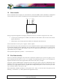
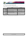
Application Guide for CRL Opto SXGA FLCOS displays Customer support information: CRL Opto Limited, Dawley Road, Hayes, Middlesex, UB3 1HH. United Kingdom Tel: +44 (0) 20 8848 6400, Fax: +44 (0) 20 8848 6653 e-mail:[email protected] http://www.crlopto.com Copyright 2003 CRL Opto Limited CONTENTS 1 2 Overview 4 The display 5 2.1 2.2 2.3 3 Greyscale & colour rendering 3.1 4 7 8 8 19 Optical principle Polarizers and polarization converters f number Near-eye systems LEDs Projection Active area Interface design Liquid crystal material Illumination Increased bit-depth Fast binary applications 19 21 21 21 22 24 25 25 25 25 26 26 27 Comparison to other display technologies 7.1 7.2 7.3 7.4 8 13 13 14 15 Possibilities and limitations 6.1 6.2 6.3 6.4 6.5 6.6 6 6 7 13 System layout Input signals and capture Timing and geometry System software Illumination and Optics 5.1 5.2 5.3 5.4 5.5 5.6 6 Rendering greyscale & colour on a digital display System 4.1 4.2 4.3 4.4 5 Data transfer Pixel functionality Ferroelectric and nematic liquid crystals Image generating methods Greyscale transfer curves Artefacts Colour gamut Contacting CRL Opto 28 28 28 29 30 31 Application Note - Application Guide CRL Opto Limited 2003 Page 2 of 31 Table of figures Figure 2.1 : CRL Opto SXGA LCOS display......................................................................................................... 5 Figure 2.2 : Active area and border ........................................................................................................................ 5 Figure 2.3 : Data bus............................................................................................................................................... 6 Figure 3.1 : Binary-weighted temporal dithering ................................................................................................... 8 Figure 3.2 : Illuminating a bitplane ...................................................................................................................... 10 Figure 4.1 : System diagram................................................................................................................................. 13 Figure 4.2 : Horizontal waveform......................................................................................................................... 14 Figure 4.3 : Vertical waveform............................................................................................................................. 15 Figure 4.4 : The SXprog user interface................................................................................................................. 17 Figure 5.1 : Polarizing beamsplitter and mirror.................................................................................................... 19 Figure 5.2 : Polarizing beam-splitter, mirror and quarter-wave plate................................................................... 20 Figure 5.3 : Example polarizer orientation ........................................................................................................... 20 Figure 5.4 : Absorbent (a) and reflective (b) sheet polarizers............................................................................... 21 Figure 5.5 : Basic near-eye viewer ....................................................................................................................... 22 Figure 5.6 : Bird-bath viewer................................................................................................................................ 22 Figure 5.7 : Pulse shapes: (a) slow-on–slow-off; (b) fast-on–slow-off; (c) slow-on–fast-off............................... 23 Figure 7.1 : Greyscale transfer curves: (a) CRT; (b) NLC; (c) FLC, DMD, PDP ................................................ 28 Figure 7.2 : Colour gamuts for various display technologies ............................................................................... 30 Table of tables Table 2-1: Nematic vs. Ferroelectric displays .................................................................................................... 7 Table 3-1 : Bitplane durations ................................................................................................................................ 9 Table 3-2 : Illumination pulse timing ................................................................................................................... 11 Table 4-1 : Horizontal timing ............................................................................................................................... 14 Table 4-2 : Vertical timing ................................................................................................................................... 15 Table 4-3 : Comparison of Master and Slave modes ............................................................................................ 16 Table 5-1 : The effect of weighting errors in bitplanes......................................................................................... 23 Table 7-1 : Comparison of methods of image generation..................................................................................... 28 Table 7-2 : Comparison of display artefacts ......................................................................................................... 29 CRL Opto Limited reserves the right to change specifications without notice. CRL Opto Limited do not accept liability for any loss or damage arising from the use of any information or particulars in this application note or from any incorrect use of the product. All maintenance and service of the products must be authorised by CRL Opto Limited. CRL Opto Limited do not accept any liability whatsoever for any loss or damage caused by service, maintenance or repair by unauthorised personnel. CRL Opto microdisplays have a variety of uses in different industries and the customer must satisfy himself that the system is suitable for his own particular purposes. While CRL Opto can give an indication of possible uses for the microdisplay, CRL Opto give no express or implied warranty that the microdisplays will be suitable for any customer's particular needs. All reasonable skill and care has been taken in compiling this application note. Whilst every effort has been made to ensure the accuracy of the information set out herein no warranty confirming such should be taken as having been given (expressly or implied). CRL Opto cannot accept responsibility for loss or damage occasioned by any person acting or refraining from action as a result of the material in this application note. Application Note - Application Guide CRL Opto Limited 2003 Page 3 of 31 1 Overview This is a guide to understanding CRL Opto SXGA ferroelectric reflective microdisplays. It contains background information about how the displays can be used, and how both the displays themselves and the interfaces work. Because the displays are most commonly supplied as part of the SXGA-R2 kit, this document will generally describe their use within such a kit, although occasionally reference will be made to other actual or potential interface systems. This is not a user manual for the specifics of the SXGA-R2 kit, but is intended to help users and potential users of the display understand its capabilities. Important: The SXGA-R2 kit is available in a number of versions which may vary from time to time. Not all features discussed here are present on every version of the kit, so potential purchasers should check the specifications of current kit versions before ordering. Because this document discusses the potential of the technology, rather than any particular system, some of the possibilities described here may not be available off-the-shelf, and will require additional custom firmware and/or hardware to be produced. Application Note - Application Guide CRL Opto Limited 2003 Page 4 of 31 2 The display The SXGA reflective LCOS display is normally supplied bonded to a flexi-circuit (known as the M49), as shown in Figure 2.1. Figure 2.1 : CRL Opto SXGA LCOS display The display has an active area of 1280×1024 pixels (illustrated in Figure 2.2), surrounded on all four sides by a 32-pixel wide border, giving a total pixel array measuring 1344×1088. Generally the active area is used for image data, and the borders are preset to black (but see also Section 6.1). By convention, the bonded edge of the display is referred to as the ‘top’. Bond wires Control circuitry row 1024 row 1055 row 0 Top border 32 Active area 1024 Total height 1088 rows Side border row 1023 row 1056 row 1087 32 Bottom border 1280 32 32 Total width 1344 columns Figure 2.2 : Active area and border Application Note - Application Guide CRL Opto Limited 2003 Page 5 of 31 2.1 Data transfer Data is transferred into the display on a 64-bit data bus, clocked at 68MHz. Control information is multiplexed onto the same bus, and a control word indicator bit (CW_ID) distinguishes between control and data words. CW_ID CK Data Bus 64 Figure 2.3 : Data bus During an upload of image data to the display, the data for each row is carried in a single burst of 21 words: • 1 control word, containing the row address, the data for the side border in that row and various control signals; followed by • 20 data words, each carrying 64 pixels of data for the 1280 pixel-wide central area. Each row thus takes 21 clock cycles, or approx. 309ns to upload. Rows can be sent in any order, and unused rows can be initialized to black at power-on time then omitted from all subsequent uploads. In most applications, the top and bottom 32 rows are handled this way, and the central 1024 rows are retransmitted on each upload. In this case, an upload will take 21×1024 = 21504 cycles, or approximately 316µs to complete. Other upload arrangements are possible — see also Section 6.1. 2.2 Pixel functionality Pixels are switched by holding the front electrode (a transparent conductive layer on the cover glass) at 2.5V, while switching the pixel mirrors to 0V or 5V. Typically, the polarising optics used to view the display are aligned so that the 0V state (state 0) appears dark, while the 5V state (state 1) is bright. Each pixel contains an SRAM latch to maintain the state of the pixel, and two spare bits of SRAM into which bitplanes of data can be pre-loaded. This data can then be copied forward from either of the spare bits to the pixel mirror in a single operation which is ‘rippled down’ through all the pixels at a rate of two rows per clock cycle. This takes 1088/2 = 544 cycles, or 8µs. Other functionality includes the ability to set all pixels to the 1 state, or invert the state of all pixels (for DC balancing – see Section 3.1.2). These operations also ripple down in 8µs. Application Note - Application Guide CRL Opto Limited 2003 Page 6 of 31 2.3 Ferroelectric and nematic liquid crystals Ferroelectric liquid crystals (FLCs) have several important differences from the more traditional nematic liquid crystal (NLC), and these are listed in Table 2-1, together with some similarities. Optical basis Switching speed Mode of operation Electrical response DC balance Colour technique Greyscale technique Greyscale response curve Nematic Ferroelectric Both types require polarized illumination, and work by rotating polarization state. From 1-2ms up to hundreds of ms. Much faster: tens of µs. Analog — continuous range of states. Digital — two stable states. Response depends on time-averaged RMS State depends on instantaneous amplitude of AC drive waveform. polarity of drive voltage. Both types require drive voltage to average zero over a period of order 100ms – 1s. Spatial — either 3 panels, or single panel with Temporal, i.e. colour sequential. coloured subpixels and a spatial filter. Inherently analog (see Section 7.2). Binary-weighted temporal dithering (see Section 3.1). Sigmoidal — may be made linear by preInherently linear. correction. Table 2-1: Nematic vs. Ferroelectric displays A comparison of FLC with other display technologies can be found in Section 7. Application Note - Application Guide CRL Opto Limited 2003 Page 7 of 31 3 Greyscale & colour rendering 3.1 Rendering greyscale & colour on a digital display 3.1.1 Binary weighting principle The SXGA display has a digital backplane, and each pixel is stable in a white or black state. In order to achieve greyscale images, the pixel is time-dithered, which means that it is rapidly switched on and off. If this switching is fast enough, the human retina will act as a low-pass temporal filter (cut-off between 40 and 120Hz depending on intensity) and a constant grey level will be perceived. The principle of dithering is illustrated in Figure 3.1. In this example, we have a four-bit grey-scale image, which allows us 16 levels, from black (0) to white (15). The time period for a frame is divided into 4 time-slots, of 8, 4, 2 and 1 fifteenth of the frame period respectively. The image is converted to a series of bit-frames, where the most significant bit b3 is displayed for 8/15 of the frame period, then b2 for 4/15 of the period, and so on. In this example, the desired intensity is 5, and the pixel is converted to a binary value of 0101, and switched on for 5 of the available 15 time units. b3 b2 b1 b0 8 4 2 1 Figure 3.1 : Binary-weighted temporal dithering The interface supplied with the display takes care of all the dithering required, with up to 8 bit-frames per colour. The actual drive waveforms used are much more complicated than those shown, for a number of reasons, but the same principle applies. For colour, as for greyscales, temporal dithering is used, but this time the illumination of the display changes colour rapidly. Depending on the interface option chosen, illumination can be changed in various ways, such as LEDs, a colour wheel, or an LCD colour shutter. The image is split into colour separations, and each colour separation is shown when the corresponding colour of light is on the display. 3.1.2 DC Balance As mentioned in Table 2-1, the liquid crystal must be DC balanced, i.e. its drive voltage averaged over a period of 100ms–1s must equal zero. When showing images using bitplanes, this means that each bitplane must be set up on the display in inverse for the same amount of time as it is in positive. In order to preserve image integrity, however, we must avoid having inverse bitplanes being perceived by the eye. This can be achieved either by turning off illumination during inverse bitplanes, or by ‘optically inverting’ the bitplane using a compensation cell (see also Section 6.4). Application Note - Application Guide CRL Opto Limited 2003 Page 8 of 31 Depending upon application, it may be more desirable either to: • to DC balance each bitplane immediately after (or before) its respective positive (adjacent balancing), or to • show several bitplanes together in positive, then balance them all at another time (grouped balancing). The standard interface supports both strategies. 3.1.3 Example drive scheme Rather than commit the system to a single method of colour rendering, the interface can be programmed to show bitplanes in any order and for any duration. The piece of firmware which determines the sequence of bitplanes is called a sequence file. The handling of sequence files is discussed in Section 4.4.2, but here we will look inside a real display sequence to see how bitplanes are shown. In this sequence, the total times for the illumination of bitplanes are as shown in Table 3-1. The interface handles 24-bit colour, and the bitplanes are designated R7–R0 (R7 is most significant, R0 is least significant) for red, G7–G0 for green and B7–B0 for blue. In many sequences, higher significance bitplanes are split into two or more separate illumination pulses, while shorter bitplanes need just one pulse. In this example sequence, R7, G7, and B7 are each split into four parts, and R6, G6 and B6 are each split in two, as shown in Table 3-1. Bitplane R7, G7, B7 R6, G6, B6 R5, G5, B5 R4, G4, B4 R3, G3, B3 R2, G2, B2 R1, G1, B1 R0, G0, B0 Time (each) in µs 1024 512 256 128 64 32 16 8 Organisation 4 × 256 2 × 256 256 128 64 32 16 8 Table 3-1 : Bitplane durations In contrast to the simplified scheme of Figure 3.1, there are gaps between the bitplanes. These are used for data setup, liquid crystal settling, and DC balancing. (In the terminology of Section 3.1.2, this example sequence uses adjacent balancing.) As can be seen in Figure 3.2, although each R6 pulse is weighted at 256µs, the data spends more time electrically present on the pixel electrode than that. The perceived weighting is correct because the display is only illuminated for 256µs during that period. The inverse data is unseen, as the display is not illuminated during that time. Application Note - Application Guide CRL Opto Limited 2003 Page 9 of 31 pixel electrode R6 +ve R6 -ve R5 +ve ≈40µs liquid crystal 100% 256µs illumination 0% Figure 3.2 : Illuminating a bitplane Application Note - Application Guide CRL Opto Limited 2003 Page 10 of 31 The illumination pulses are delivered over the course of the frame period as given in Table 3-2. (Both the pulse durations and the LED on and off times are rounded to the nearest microsecond, so any apparent "off-by-one" errors are the result of rounding.) Bitplane R7 R0 R7 R1 R7 R2 R7 R3 R6 R4 R6 R5 G7 G0 G7 G1 G7 G2 G7 G3 G6 G4 G6 G5 B7 B0 B7 B1 B7 B2 B7 B3 B6 B4 B6 B5 Pulse start (µs) 654 1236 1324 1907 2010 2593 2729 3312 3512 4094 4422 5006 5589 6172 6260 6842 6946 7529 7664 8248 8448 9030 9358 9942 10525 11108 11195 11778 11882 12464 12600 13184 13383 13966 14294 14876 Pulse end (µs) 910 1244 1580 1923 2266 2625 2984 3376 3768 4222 4678 5262 5845 6180 6516 6858 7202 7561 7920 8312 8704 9158 9614 10197 10781 11116 11451 11794 12138 12496 12856 13248 13639 14094 14550 15132 Table 3-2 : Illumination pulse timing There is also a lot of work going on behind the scenes. Before each bitplane of data can be applied to the pixel electrodes, it must first be uploaded from the interface onto the display’s backplane. This is done using a 4.35Gb/s link along the flexi, and takes approximately 316µs per bitplane. Because it would be undesirable to have the pixels in a mixed state for this long, the upload copies data into one of two SRAM latches behind the pixel electrode, where it can be held until required. This means that data upload can be running one or two bitplanes ahead of bitplane display, and ensures that the next bitplane of data is always available when needed, even after a bitplane whose weighting is much less than Application Note - Application Guide CRL Opto Limited 2003 Page 11 of 31 the 316µs upload time. It also means that split bitplanes only need to be uploaded once, provided that a latch can be kept free for that bitplane over its entire span. 3.1.4 Duty cycles The example sequence of Section 3.1.3 has each LED switched on for a total of 2039µs, out of a frame period of 16661µs. This gives us a duty cycle of 12.24% per colour, or 36.72% overall. 3.1.5 Varieties of drive scheme The sequence described in Section 3.1.3 above is just one example how a drive scheme can be constructed. Other sequences can differ from this in a number of ways: • Red, green and blue bitplanes may be interleaved instead of grouped together. • Illumination can be spread across the whole frame period, or concentrated into a smaller part of it. • Some sequences use more, or less, splitting of high significance bitplanes. Bitplanes may be split into equal or unequal parts. • As mentioned in Section 3.1.2, grouped balancing can be used, which means that positive bitplanes are grouped together, and DC balanced at another time. This technique is often used in systems which contain a colour wheel and/or compensation cell, in order to work with continuous light sources. Grouped balancing generally requires two uploads per bitplane, rather than the one upload needed when adjacent balancing is used. • The number of bitplanes may be reduced and traded for a faster refresh rate e.g. 120 or 180Hz. • Drive schemes may vary more radically than this — further possibilities are discussed in Section 6. Application Note - Application Guide CRL Opto Limited 2003 Page 12 of 31 4 System The SXGA-R2 interface is based upon the MDD1304B display driver ASIC, which is a low-cost 24-bit colour driver specifically designed for our SXGA LCOS displays. Other interfaces are possible — see also Section 6.2. The remainder of this section applies to the standard SXGA-R2 system, unless stated otherwise. 4.1 System layout The SXGA-R2 display system takes an incoming computer graphics signal, normally in VESA standard SXGA60 format, and shows it in 24-bit colour on the SXGA LCOS display, at 60 frames per second. Optionally, a PC can be connected by an RS-232 serial cable to configure the interface (see Section 4.4.4). This PC may also be the image source, or not, as the user prefers. PC for configuration RS 232 SXGA 60Hz image source (e.g. PC) CRL Opto SXGA Interface VGA or DVI cable CRL Opto SXGA display Proprietary format Figure 4.1 : System diagram Depending on the firmware version on the board (see also section 4.4.1), it may also be possible to feed in lower resolution images (VGA, SVGA, XGA, HDTV 720p etc.) and show them in a window within the SXGA display. 4.2 Input signals and capture Image data may be fed in via a 15-pin D-type VGA connector, or through a DVI connector. When DVI is used, the digital RGB level shown on the display will match precisely that generated by the software on the image source. The pixel clock is carried by a twisted pair in the DVI cable. When a VGA connector is used, the signal undergoes digital-to-analog (D/A) conversion on the PC graphics card, and analog-to-digital (A/D) conversion on the interface. Such a process is always imprecise, due to component tolerances and analog noise. As a result, digital levels may no longer match exactly. In many applications, this doesn’t matter much, but in a few cases it could be important (see also section 6). When analog input is used, the pixel clock is not transmitted on the cable — the analog capture chip reconstructs the pixel clock from Hsync using a PLL multiplier. Application Note - Application Guide CRL Opto Limited 2003 Page 13 of 31 4.3 Timing and geometry The SXGA60 input signal, whether transmitted through DVI or VGA, should have the same timing. The timing reference, for horizontal and vertical timing respectively, is the leading edge of the corresponding sync signal. Since SXGA60 uses positive-going sync pulses, this is the rising edge. The horizontal waveform is as shown in Figure 4.2. total line width 1688 pixels Hsync Video data back porch 248 pixels active data 1280 pixels front porch 48 pixels Sync width 112 pixels Figure 4.2 : Horizontal waveform The nominal pixel clock is 108MHz, which leads to the timings given in Table 4-1. Note that the number of pixel cycles is definitive, while the absolute times or frequencies are derived and approximate. The VESA standard allows the pixel clock frequency to drift by ±0.5%. When this happens, the number of cycles of the pixel clock for each of the other parameters is maintained, so their absolute times will vary in the same proportion. Parameter Hsync Hsync width Back porch Active data Front porch Pixel clock cycles 1688 112 248 1280 48 Approx. time / frequency 15.63µs / 63.981kHz 1.037µs 2.296µs 11.85µs 0.444µs Table 4-1 : Horizontal timing Application Note - Application Guide CRL Opto Limited 2003 Page 14 of 31 Vertical timings are shown in Figure 4.3 and Table 4-2. total height 1066 lines Vsync Video data back porch 38 lines active data 1024 lines front porch 1 line Sync width 3 lines Figure 4.3 : Vertical waveform Parameter Vsync period Vsync width Back porch Active data Front porch Lines 1066 3 38 1024 1 Approx. time / frequency 16.661ms / 60.020Hz 46.889µs 593.93µs 16.005ms 15.630µs Table 4-2 : Vertical timing With appropriate firmware, the MDD1304B driver chip can accept other video resolutions and frame rates, including custom video modes, with any bit-depth up to 24 and any pixel clock rate up to 108MHz. Video with a lower resolution can be shown in a window, in the middle of the display, containing the same number of pixels as the source image. The timing of bit-planes on the display is derived from the incoming Vsync signal, and will always have a fixed phase relationship to it. The standard system does not, at time of writing, support re-sizing or frame rate conversion (but see also Section 6.2). 4.4 System software 4.4.1 Micro code The MDD1304B ASIC contains an embedded microcontroller which has access to the configuration registers inside the chip, and also to its ports, which can be used for controlling other devices in a system. The firmware for this micro is called the application program (AP), and is stored in an external serial flash device. The ASIC can be configured either to control a complete system (acting as system master) or to be a subsidiary (slave) chip controlled by a separate micro. The differences are listed in Table 4-3. Application Note - Application Guide CRL Opto Limited 2003 Page 15 of 31 Master mode Designed for CRL Opto evaluation kit boards, where a known set of external chips is present. Avoids need for external micro to control system. ASIC configures all of its own settings at power-on from flash memory. ASIC controls other programmable chips. User can alter configuration using SXprog utility. ASIC firmware must be changed (by CRL Opto) if new programmable chips are added to system. Control protocol is proprietary. Supplied firmware supports a fixed video format (e.g. SXGA, HDTV etc.), or a finite number of predetermined video formats, depending on firmware version. Drive sequences are stored and managed by ASIC. Colour look-up tables configured by a fixed, built-in function which only supports gamma control. ASIC will automatically switch to test pattern when video signal is absent, thus ensuring DC balance. Slave Mode Designed for system integrators, who will determine system architecture for themselves. System controlled by external micro. ASIC defaults to test image (colour bars), and awaits further instructions. ASIC does not control any other chips. Configuration is by industry-standard two-wire interface, not user interface. System integrator changes firmware for external micro if new programmable chips are added to system. Control protocol is documented in data sheet. System integrator has documentation to allow them to support any video format they choose (within hardware limitations) including non-standard formats. Drive sequences are stored and managed by external micro. System master has complete freedom to define arbitrary contents for look-up tables. System master has responsibility to monitor video, and put display into DC-safe standby mode when absent. Table 4-3 : Comparison of Master and Slave modes In general, systems based on the M43 interface will be shipped with master mode code, while slave mode is better suited to custom interfaces. We are not able to support users wishing to generate their own micro code, but slave mode should have all the flexibility needed for system integrators. In the event that custom micro code is required, this can be developed for users by CRL Opto. SXGA-R2 kits are supplied pre-programmed with master mode code, and can be upgraded with new micro code in the field, using the SXprog utility (see Section 4.4.4). 4.4.2 Sequences The sequence is a piece of firmware which determines the order and timing of bitplanes. As mentioned in Section 3.1.5, there is enormous flexibility in the way sequences can be created. Sequences are produced in-house by CRL Opto, using special software tools. At time of writing, there are no plans to make these tools available to third parties, but a custom sequence-building service is available from CRL Opto. SXGA-R2 kits are supplied pre-programmed with one or more general purpose sequences, and can be upgraded with new sequence files in the field, using the SXprog utility (see Section 4.4.4). The SXGA-R2 kit can store up to 10 sequences in its onboard flash filing system and, using SXprog, any loaded sequence can be made the default for loading on power-up. Application Note - Application Guide CRL Opto Limited 2003 Page 16 of 31 4.4.3 EDID code EDID (Extended Display Identification Data) files are small data structures which can be uploaded by a PC or other graphics source through the VGA or DVI cable. Most present-day CRT monitors, flat-panel displays and projectors contain an EDID, and the SXGA-R2 kit is no exception. The EDID structure contains information such as the make and model of monitor and the resolutions and frame rates it can accept. EDID code is not essential for analog video connections, but is usually required by DVI graphics cards before a DVI signal will be produced. EDID is a trademark of the Video Electronics Standards Association (VESA) and the standard can be obtained from them at http://www.vesa.org/. Several third-party EDID editors are available, such as “EDID Editor” from ViewSonic (http://www.viewsonic.com/). SXGA-R2 kits are supplied pre-programmed with EDID code, and can be upgraded with new EDID files in the field, using the SXprog utility (see Section 4.4.4). 4.4.4 SXprog SXprog is a utility program for configuring and reprogramming the SXGA-R2 kit through an RS-232 cable. It presents a user interface as shown in Figure 4.4. Figure 4.4 : The SXprog user interface SXprog’s capabilities include: • re-programming of micro code, sequences and EDID code, • adjustment of LED brightness and gamma look-up tables, • colour wheel control and miscellaneous other functions. A separate user manual is available for SXprog, describing its features in detail. Note: It is not necessary to connect SXprog to the SXGA-R2 kit every time it is powered on — only when the configuration is to be changed. Application Note - Application Guide CRL Opto Limited 2003 Page 17 of 31 4.4.5 Supported platforms SXprog is currently supported under Windows 98 and XP. It is not recommended for Windows NT or 2000, due to difficulties with the use of the serial port. It has not been tested under Windows 95 or ME. A Linux version of SXprog is under development. Application Note - Application Guide CRL Opto Limited 2003 Page 18 of 31 5 Illumination and Optics 5.1 Optical principle To understand how the FLCOS microdisplay works, it may help to consider the following: If a light source, a mirror, and a polarizing beamsplitter (PBS) are arranged as shown in Figure 5.1, no light will reach the observer. The sequence of events is as follows: 1. 2. 3. 4. 5. The illuminator produces unpolarized light, which hits the PBS. The P-polarized component passes through the PBS and leaves the system as waste light. The S-polarized component is reflected by the PBS onto the mirror. The light reflected by the mirror is still S-polarized. The PBS reflects the S-polarized light back to the illuminator, and no light reaches the observer. Illuminator 1 (S+P) 5 (S) Observer 3 (S) 4 (S) 2 (P) Figure 5.1 : Polarizing beamsplitter and mirror In a second example (not illustrated), a quarter-wave plate (λ/4) is inserted between the mirror and beam-splitter, and orientated at an angle of 0° relative to the S-polarized light (i.e. aligned with it). This has no effect. The light returning from the mirror–quarter-wave plate combination is still S-polarized. In a third example (Figure 5.2), the quarter-wave plate is rotated by 45° relative to the S-polarized light. In this case, there is a new sequence of events, as follows: 1. 2. 3. 4. 5. The illuminator produces S- and P-polarized light, which hits the PBS (as before). The P-polarized light passes through the PBS and leaves the system as waste light (again as before). The S-polarized light is reflected by the PBS onto the mirror, this time via the quarter-wave plate, so it is circularly polarized when it reaches the mirror. The reflected light, is circularly polarized in the opposite direction, and having passed through the quarter-wave plate a second time, is once again linearly polarized, but this time rotated by 90°, i.e. Ppolarized. The PBS passes the P-polarized light through to the observer. Application Note - Application Guide CRL Opto Limited 2003 Page 19 of 31 Illuminator 1 (S+P) Mirror Observer 3 (S) 4 (P) 5 (P) 2 (P) Quarter-wave plate Figure 5.2 : Polarizing beam-splitter, mirror and quarter-wave plate The liquid crystal layer in the display acts like an electrically switchable quarter-wave plate. In the off state it is aligned with the incoming S-polarized light, while in the on state it is at an angle, thus causing light to reach the observer. Each pixel is individually switchable, allowing the creation of images. 5.1.1 Orientation A suitable orientation for the PBS and microdisplay is as shown in Figure 5.3. A correct polarity image will also be obtained at 90° increments from this position. The contrast ratio of the system is sensitive to the accuracy of orientation of the microdisplay and PBS. It is also possible to use the P-polarized beam to illuminate the display, rather than the S-polarized beam as illustrated, and with some types of PBS this may be preferable. 1280 SXGA 1024 S illuminator P S+P PBS Figure 5.3 : Example polarizer orientation Application Note - Application Guide CRL Opto Limited 2003 Page 20 of 31 5.2 Polarizers and polarization converters A polarizing beamsplitter is seldom if ever perfect, i.e. the transmitted light is not quite 100% P-polarized and the reflected light is not quite 100% S-polarized. MOXTEK sheet PBSs generally have better performance than glass-cube PBSs, which in turn generally out-perform polymer sheet PBSs. In order improve the contrast ratio of a real system, it is common practice to add a pre-polarizer to ensure that the light reaching the PBS is already mostly in the desired S-polarized state. Normal-incidence sheet polarizers are available in absorbent and reflective varieties, as shown in Figure 5.4. In low-power systems, pre- and clean-up polarizers are usually made from sheet absorbent material. High power systems use reflective polarizers (for pre-polarization especially) as these are less prone to burning out. S+P S+P S P absorbed S P reflected (b) (a) Figure 5.4 : Absorbent (a) and reflective (b) sheet polarizers A separate application note is available describing the use of CRL Opto displays with MOXTEK ProFluxTM polarizers. As an alternative to pre-polarizers, a variety of types of polarization converter are available. These are devices which separate light into S and P orientation, and then convert the light in one polarization state into the other. By this means, unpolarized light from the source can be converted to useful plane polarized light with over 75% efficiency. 5.3 f number The thin cell gap of the CRL Opto microdisplay, allows it to be used right down to f1.8 — much lower than most other comparable technologies. 5.4 Near-eye systems Near-eye systems will almost always use LED illumination (see Section 5.5). An example configuration for a near-eye system is shown in Figure 5.5. Application Note - Application Guide CRL Opto Limited 2003 Page 21 of 31 Pre-polarizer Telecentric Illuminator Clean-up polarizer Observer Display Polarizing Beamsplitter Magnifying Lens Figure 5.5 : Basic near-eye viewer An alternative near-eye system, known as the ‘bird-bath’, uses a magnifying mirror instead of a lens, and a nonpolarizing as opposed to polarizing beamsplitter as illustrated in Figure 5.6. A Bird-bath viewer can also be built with a polarizing beamsplitter, but in this case a quarter-wave plate must be added to the magnifying mirror. Pre-polarizer Telecentric Illuminator Clean-up polarizer Observer Magnifying Mirror Display Beamsplitter (non-polarizing) Figure 5.6 : Bird-bath viewer 5.5 LEDs These are used principally in near-eye applications, but the recent advent of high-powered LEDs is making LED-based projection a reality. Although white LEDs are available, the colour sequential nature of display makes it much more effective to have separately switchable red, green and blue light sources. 5.5.1 Switching speed The fast switching performance of LEDs makes them ideal illuminators for the CRL Opto SXGA LCOS display. The SXGA-R2 kit switches LEDs on and off in under 500ns, but switching as fast as this is not essential. What is important is that the amount of light generated in each pulse remains in correct proportion to the other pulses in the frame. Application Note - Application Guide CRL Opto Limited 2003 Page 22 of 31 Some applications involve using laser diodes, or much higher-powered LEDs than those supplied with a standard kit — and these might perhaps switch more slowly than the usual LEDs. If a light source takes several microseconds to turn on, and an equal number to turn off (and with a similarly shaped curve) then there should be no problem with the greyscale. If, however, the light source is much slower to turn on than off, or vice versa, then the effective pulse width can be distorted. Figure 5.7 shows the effect that asymmetrical switching can have on an 8µs least-significant bitplane (LSB). The effect on higher significance bitplanes is in absolute terms the same, but proportionally less — and here lies the problem. Some greyscale levels have the pixel switched on during more pulses than others. Assuming, for simplicity, that there is no splitting of bitplanes (and in some sequences, there is none), there will be 8 pulses per colour. A pixel at level 0 will be switched on during none of them, while a pixel at level 255 (0xFF) will be switched on during all of them. Some neighbouring bitplanes have very different pulse counts, for example level 127 (0x7F) is on during seven pulses, while level 128 (0x80) uses just one pulse. Let us assume, for example, that a hypothetical light source turns on much faster than off, to the extent that the LSB has 20% more light than it should have. Every other bitplane will also be too long, but by 0.2 LSBs rather than 20% of its own length. This will make level 127, with its seven pulses, long by 7×0.2 = 1.4 LSBs; level 128, with its single pulse will be long by 1×0.2 = 0.2LSBs. The effect on step size between these two grey-levels is shown in Table 5-1. The end result of distorted weighting is the appearance of false contours in smoothly shaded images, especially at particular steps such as 127-128, 63-64, and 31-32. If, however, a given light source is known to have significantly asymmetrical switching, this can be compensated for by building a new sequence with adjusted pulse widths. Using the new special sequence, it should once more be possible to achieve smooth shading. 8µs LED enable signal (a) illumination area under curve OK (b) illumination area under curve too large (c) illumination area under curve too small Figure 5.7 : Pulse shapes: (a) slow-on–slow-off; (b) fast-on–slow-off; (c) slow-on–fast-off Ideal ideal-0.2 ideal+0.2 level 127 (0x7F) 64.0+32.0+16.0+8.0+4.0+2.0+1.0 = 127.0 63.8+31.8+15.8+7.8+3.8+1.8+0.8 = 125.6 64.2+32.2+16.2+8.2+4.2+2.2+1.2 = 128.4 level 128 (0x80) 128.0 = 128.0 127.8 = 127.8 128.2 = 128.2 step size 1.0 2.2 -0.2 Table 5-1 : The effect of weighting errors in bitplanes Application Note - Application Guide CRL Opto Limited 2003 Page 23 of 31 5.5.2 High-power LEDs A number of vendors (e.g. Lumileds) are now offering LED emitters in the high tens of lumens output (or low tens for blue). The LED circuitry in the SXGA-R2 kit (at time of writing) is set up to provide peak currents of up to 250mA for LEDs or LED arrays with forward voltage (plus cable IR drop) of up to 6.7V. Component value changes can provide modestly increased common anode voltage and peak current. The circuitry can be further modified, on request, to support peak currents up to 6A (mean up to 1A), or forward voltages up to 48V, with an external common anode supply. Beyond this, custom drive circuitry will be required, and can be controlled by red, green and blue enable signals exported from the circuit board. (Exporting enable signals may require modifications to the kit, depending on its version.) Duty cycles per LED are typically in the range of 7 to 14% (depending on sequence), so LEDs can be driven at peak currents often much higher than their continuous rated currents. 5.6 Projection Like nematic microdisplays, CRL Opto SXGA LCOS microdisplays can be used in three-channel projection system. Unlike most nematic displays, however, our ferroelectric displays can also be used in single-channel colour sequential systems. CRL Opto has demonstrated a prototype LED-illuminated projector, using high-power LEDs (see Section 5.5.2). Energy efficiency is very good and image quality (particularly colour gamut) is exceptional (see also Section 7). Based on this prototype, an LED projection evaluation kit is planned — contact CRL Opto Sales for an update. Application Note - Application Guide CRL Opto Limited 2003 Page 24 of 31 6 Possibilities and limitations This section explores potential special applications of the technology which are not supported by the standardrecipe displays or by the interface electronics normally supplied, but which might be possible with a customised display or interface. In this section, the description of a feature or application as possible does not imply that a suitable product is available, or even that it is likely to become available as a standard product. The intention here is simply to separate ideas which could be technically feasible from those which are not. We also aim to distinguish here between limitations of the interface firmware, the interface hardware, the display recipe and the display backplane. 6.1 Active area In most applications, all border pixels are set to black, and most interface systems will support only this functionality. It would be possible, though, with an appropriate interface, to address individually the central 1280 pixels of all 1088 rows; the pixels in the side borders are addressable two at a time in horizontally adjacent pairs. It is also possible to use fewer than 1024 rows (e.g. 1280×720 for a 16:9 aspect ratio), and with appropriate firmware each upload can be completed in a proportionally smaller time. (This feature is known as letterboxing.) Shorter uploads allow more flexibility in the construction of a drive scheme (see Section 3.1). 6.2 Interface design The SXGA-R2 kit is based around the MDD1304B display driver ASIC, which is a low-cost 24-bit colour driver specifically designed for our SXGA LCOS displays. By adding to the standard kit, support for many other features could be provided, such as the following: • • • • • • • image re-sizing, frame rate conversion and re-synchronization, colour-space manipulation (over and above the gamma correction already provided), image conditioning and filtering, image warping, on-screen display, picture-in-picture and genlocking. Other interface options, e.g. FPGA-based systems can also be made available where extra flexibility is required for non-standard applications. In such a system, the images used need not necessarily come from a video stream, but might instead be pre-loaded by a remote or embedded processor. 6.3 Liquid crystal material Display devices are normally filled with ferroelectric liquid crystal (see also Section 2.3). To optimise the SLM for a particular application, it is often necessary to modify the cell spacing, or the liquid crystal filling. In some applications, for example, there might be an advantage in using a nematic or a guest-host Application Note - Application Guide CRL Opto Limited 2003 Page 25 of 31 material. The SXGA backplane is capable of driving such materials, although its performance (in terms of bitdepth etc.) has not yet been characterised in this context. Although the microdisplay is generally used as a display device, it can be used as a spatial light modulator (SLM) in a diverse range of optical systems. These applications include adaptive optics, imaging, microscopy, optical communications, laser machining, and optical trapping. As an SLM, the device can be configured to operate either as a binary amplitude (0,1), or a pure binary phase (0, π) modulator. 6.4 Illumination 6.4.1 Arc lamps and colour wheels Apart from pulsed light sources, it is also possible to use continuous sources such as arc lamps, in conjunction with colour wheels and/or compensation cells, and the SXGA-R2 contains circuitry to support such applications. The SXGA LCOS display has been successfully used in single-channel systems with lamps of over 10,000 lumens at source. As the SXGA LCOS display is a reflective device, its rear surface can be used for heat extraction, making it easier to cool than a transmissive device in very high-power applications. 6.4.2 Wavelength Standard devices are designed to work across the visible spectrum, and are well suited to single-panel full-colour applications. Ultra violet applications are not currently viable, as the device lifetime is affected when exposed to highintensity light at wavelengths of 410nm or less. When used with illumination sources (e.g. arc lamps) which generate a strong UV or near-UV component, a filter is used to remove dangerous wavelengths. Infra-red applications are viable, but require a non-standard display recipe. Displays optimised for use at 1550nm (telecomms) and 1064nm (Nd:YAG) are under development at time of writing. 6.5 Increased bit-depth The colour depth of a binary-weighted three-colour scheme is constrained by the M43 interface electronics (and the MDD1304B ASIC thereon) to 24 bits. A custom interface might allow this to be increased slightly, but the bandwidth of the data bus to the backplane means that only a modest increase could be obtained while retaining full SXGA resolution. Reducing the height of the image allows the upload of each bitplane to be completed faster, and potentially higher colour depth. The maximum achievable bit-depth in monochrome applications is not yet confirmed, but is estimated to be in the range of 10-12 bits. Higher bit-depth monochrome images could be fed into the standard interface hardware using false-colour DVI; alternatively a custom analog capture module could be added. Applying these techniques to a three-channel system (with three interfaces) colour at more than 24 bits could be achieved. It is also possible, by changing firmware, to trade bits of one colour for bits of another. This also requires the user to generate false-colour images and feed them in through DVI. Application Note - Application Guide CRL Opto Limited 2003 Page 26 of 31 6.6 Fast binary applications Bitplanes need not necessarily be weighted in a binary greyscale pattern. For example, by compositing 24 onebit images into a 24-bit false-colour image and feeding it in through DVI, 1440 evenly spaced one-bit images per second can be achieved. (Analog input is not recommended for these applications, for reasons discussed in Section 4.2.) Applications include printing, telecomms, volumetric displays and optical correlators. Application Note - Application Guide CRL Opto Limited 2003 Page 27 of 31 7 Comparison to other display technologies In this section we compare our FLC technology to other display technologies, namely cathode ray tube (CRT), nematic liquid crystal (NLC), digital micromirror device (DMD) and plasma display panel (PDP). 7.1 Image generating methods Greyscale Colour Large image Channels reqd. (if projected) Light modulation Phase mode available CRT Analog Spatial Direct/Projected 3 NLC Analog Spatial Direct/Projected 3 FLC Digital Temporal Projected 1 or 3 DMD Digital Temporal Projected 1 or 3 PDP Digital Spatial Direct n/a Emissive No Reflective or Transmissive Yes Reflective1 Yes Reflective No Emissive No 1 Reflective in CRL Opto displays, but FLCs are also used in transmissive cells, shutters etc. Table 7-1 : Comparison of methods of image generation 7.2 Greyscale transfer curves The greyscale transfer curve is, roughly speaking, the relationship between the luminance signal going into the display and the amount of light coming out. This is usually expressed as a graph with signal input on the X axis and light output on the Y axis. Some examples are shown in Figure 7.1. light output light output light output input signal (a) input signal (b) input signal (c) Figure 7.1 : Greyscale transfer curves: (a) CRT; (b) NLC; (c) FLC, DMD, PDP The CRT gives an exponential curve called a gamma curve. The name is derived from its usual equation y = xγ , where x and y are normalized over a range of 0 to 1. A typical figure for γ is around 2.4. Nematic liquid crystals inherently have a sigmoidal transfer curve, but NLC based displays often contain lookup tables to linearize the curve. CRL Opto FLC displays, along with their DMD and PDP counterparts, have a linear transfer function. Because some image sources pre-compensate their images to produce linear fades on a CRT (this is called gamma correction), some systems, including the SXGA-R2 kit, contain gamma-adjustment look-up tables to allow the displays to mimic the transfer curve of a CRT. Application Note - Application Guide CRL Opto Limited 2003 Page 28 of 31 Some transmission artefacts (as opposed to display artefacts, discussed in Section 7.3), such as ‘blocking’ in dark areas of MPEG-compressed video streams, can be more visible in linear-greyscale devices (or in linearizedgreyscale systems), because the starting gradient is higher than in the sigmoidal or gamma curve (see also Section 7.2). SXGA-R2 kits usually come pre-adjusted to a gamma of 1.4, which is sufficient to make MPEG blockiness invisible, while still retaining the vibrancy which comes from low gamma. 7.3 Artefacts Every display technology is susceptible to artefacts, but the type and severity varies from type to type. In the table below, X means that the problem occurs and is difficult or impossible to prevent or significantly reduce; x means that the problem occurs but that techniques exist to significantly reduce it; an empty box means the artefact is not a problem to begin with. Moiré smearing (trails) temporal skewing False contours2 wagon wheel CRT X (x) x X X1 X NLC X FLC DMD PDP X x x x X X X Notes Fine textures can produce coarser-texture artefacts. Occurs if material has some persistence lasting longer than one frame period. Most modern CRT phosphors are fast enough to avoid this, majority of NLCs are not. Can affect any technology in which data is shown by progressive scan down the display over a frame period. Can be combated by appropriate design of drive scheme. This takes its name from old Wild West films in which the wheels of a fast-moving wagon appear to be turning backwards. This was first noticed on film movies, and also affects every other frame-based display technology. 1 Affects TFT transmissive NLC, but not LCOS reflective NLC. Static false contours can appear on any display technology if the image source has insufficient bit depth. 2 Table 7-2 : Comparison of display artefacts Application Note - Application Guide CRL Opto Limited 2003 Page 29 of 31 7.4 Colour gamut No display technology can replicate the entire range of colours perceivable by the human visual system, but some technologies come closer than others. The range of colours which a display can render is called its gamut, and in RGB systems this is generally represented as a triangle on a CIE chromaticity chart. (Some image transmission media impose restrictions of their own, leading to a non-triangular system gamut, but we will not cover that here.) In general, LED-illuminated systems will have the best gamut (especially in red and green), as shown in Figure 7.2 — the precise gamut depends upon choice of LEDs. Typical mass-market CRT phosphors have a smaller gamut (again, as shown in Figure 7.2), although high-end specialist CRTs can have significantly wider gamut than an ordinary TV or monitor. Plasma panels are comparable to CRTs, although the choice of phosphors is currently more restricted. LED CRT Lamp Figure 7.2 : Colour gamuts for various display technologies The poorest gamuts come from systems which generate white light, then split the spectrum into three broad bands. This applies both to colour-wheel–based systems (Section 6.4.1) and three-channel lamp-based systems. Gamut is less sensitive to microdisplay type, where microdisplays are used, although it is worth observing that low contrast ratio tends to reduce saturation of all colours. Application Note - Application Guide CRL Opto Limited 2003 Page 30 of 31 8 Contacting CRL Opto CRL Opto technical support may be contacted as shown below: Telephone: +44 (0) 208 848 6400 Facsimile: +44 (0) 208 848 6653 E-mail: [email protected] Website: http://www.crlopto.com Address: CRL Opto Limited Dawley Road Hayes Middlesex UB3 1HH United Kingdom Application Note: SXGA Application Guide 5043-62000 Version 1.0 Document no.: 915/0305/01A Dated: 21/07/03. Document release no. SC 11/03 Copyright 2003 CRL Opto Limited. Registered in Scotland no: SC 174872. CRL Opto Limited reserves the right to change specifications without notice. CRL Opto Limited do not accept liability for any loss or damage arising from the use of any information or particulars in this application note or from any incorrect use of the product. All maintenance and service of the products must be authorised by CRL Opto Limited. CRL Opto Limited do not accept any liability whatsoever for any loss or damage caused by service, maintenance or repair by unauthorised personnel. CRL Opto microdisplays have a variety of uses in different industries and the customer must satisfy himself that the system is suitable for his own particular purposes. While CRL Opto can give an indication of possible uses for the microdisplay, CRL Opto give no express or implied warranty that the microdisplays will be suitable for any customer's particular needs. All reasonable skill and care has been taken in compiling this application note. Whilst every effort has been made to ensure the accuracy of the information set out herein no warranty confirming such should be taken as having been given (expressly or implied). CRL Opto cannot accept responsibility for loss or damage occasioned by any person acting or refraining from action as a result of the material in this application note. Application Note - Application Guide CRL Opto Limited 2003 Page 31 of 31