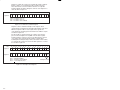
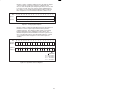
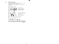
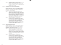
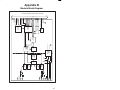
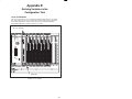
1
 ! ! ! " ! WARNING
THIS UNIT AND ITS ASSOCIATED EQUIPMENT MUST BE INSTALLED,
ADJUSTED AND MAINTAINED BY QUALIFIED PERSONNEL WHO ARE
FAMILIAR WITH THE CONSTRUCTION AND OPERATION OF ALL EQUIPMENT
IN THE SYSTEM AND THE POTENTIAL HAZARDS INVOLVED. FAILURE TO
OBSERVE THESE PRECAUTIONS COULD RESULT IN BODILY INJURY.
WARNING
UNEXPECTED MACHINE MOVEMENT MAY BE THE RESULT OF INSERTING OR
REMOVING THIS MODULE OR ITS CONNECTING CABLES. POWER SHOULD BE
REMOVED FROM THE MACHINE BEFORE INSERTING OR REMOVING THE
MODULE OR ITS CONNECTING CABLES. FAILURE TO OBSERVE THESE
PRECAUTIONS COULD RESULT IN BODILY INJURY.
CAUTION
THIS MODULE CONTAINS STATICĆSENSITIVE COMPONENTS. CARELESS
HANDLING CAN CAUSE SEVERE DAMAGE.
DO NOT TOUCH THE CONNECTORS ON THE BACK OF THE MODULE. WHEN
NOT IN USE, THE MODULE SHOULD BE STORED IN AN ANTIĆSTATIC BAG.
THE PLASTIC COVER SHOULD NOT BE REMOVED. FAILURE TO OBSERVE
THIS PRECAUTION COULD RESULT IN DAMAGE TO OR DESTRUCTION OF
THE EQUIPMENT.
! ! ! # $ !
! $
%% !
$ ! $ Table of Contents
1.0
Introduction . . . . . . . . . . . . . . . . . . . . . . . . . . . . . . . . . . . . . . . . . . . . . . . 1Ć1
2.0
Mechanical/Electrical Description . . . . . . . . . . . . . . . . . . . . . . . . . . . 2Ć1
2.1 Mechanical Description . . . . . . . . . . . . . . . . . . . . . . . . . . . . . . . . . . . 2Ć1
2.2 Electrical Description . . . . . . . . . . . . . . . . . . . . . . . . . . . . . . . . . . . . . 2Ć1
3.0
Installation . . . . . . . . . . . . . . . . . . . . . . . . . . . . . . . . . . . . . . . . . . . . . . . .
3.1 Wiring . . . . . . . . . . . . . . . . . . . . . . . . . . . . . . . . . . . . . . . . . . . . . . . . . .
3.2 Initial Installation . . . . . . . . . . . . . . . . . . . . . . . . . . . . . . . . . . . . . . . . .
3.3 Module Replacement . . . . . . . . . . . . . . . . . . . . . . . . . . . . . . . . . . . . .
3Ć1
3Ć1
3Ć1
3Ć4
4.0
Programming . . . . . . . . . . . . . . . . . . . . . . . . . . . . . . . . . . . . . . . . . . . . . .
4.1 Register Organization . . . . . . . . . . . . . . . . . . . . . . . . . . . . . . . . . . . .
4.2 Configuration . . . . . . . . . . . . . . . . . . . . . . . . . . . . . . . . . . . . . . . . . . .
4.3 Reading And Writing Data In Application Tasks . . . . . . . . . . . . . .
4.3.1 BASIC Task Example . . . . . . . . . . . . . . . . . . . . . . . . . . . . . . .
4.3.2 Control Block Task Example . . . . . . . . . . . . . . . . . . . . . . . . .
4.4 Using Interrupts in Application Tasks . . . . . . . . . . . . . . . . . . . . . . .
4.4.1 BASIC Task Example . . . . . . . . . . . . . . . . . . . . . . . . . . . . . . .
4.4.2 Control Block Task Example . . . . . . . . . . . . . . . . . . . . . . . . .
4.5 Restrictions . . . . . . . . . . . . . . . . . . . . . . . . . . . . . . . . . . . . . . . . . . . . .
4.5.1 Writing Data to Registers . . . . . . . . . . . . . . . . . . . . . . . . . . . .
4.5.2 Use in Remote I/O Racks . . . . . . . . . . . . . . . . . . . . . . . . . . .
4.5.3 Initializing or Updating Filter Registers . . . . . . . . . . . . . . . .
4Ć1
4Ć1
4Ć4
4Ć4
4Ć5
4Ć6
4Ć6
4Ć7
4Ć8
4Ć9
4Ć9
4Ć9
4Ć9
5.0
Diagnostics And Troubleshooting . . . . . . . . . . . . . . . . . . . . . . . . . . .
5.1 Incorrect Data . . . . . . . . . . . . . . . . . . . . . . . . . . . . . . . . . . . . . . . . . . .
5.2 Bus Error . . . . . . . . . . . . . . . . . . . . . . . . . . . . . . . . . . . . . . . . . . . . . . .
5.3 Interrupt Problems . . . . . . . . . . . . . . . . . . . . . . . . . . . . . . . . . . . . . . .
5.3.1 No Interrupts . . . . . . . . . . . . . . . . . . . . . . . . . . . . . . . . . . . . . .
5.3.2 Hardware Event TimeĆOut . . . . . . . . . . . . . . . . . . . . . . . . . . .
5.3.3 Hardware Event Count Limit Exceeded . . . . . . . . . . . . . . .
5.3.4 Illegal Interrupt Detected . . . . . . . . . . . . . . . . . . . . . . . . . . . .
5Ć1
5Ć1
5Ć2
5Ć3
5Ć3
5Ć3
5Ć4
5Ć4
I
Technical Specifications . . . . . . . . . . . . . . . . . . . . . . . . . . . . . . . . . . . . . . AĆ1
Module Block Diagram . . . . . . . . . . . . . . . . . . . . . . . . . . . . . . . . . . . . . . BĆ1
Field Connections . . . . . . . . . . . . . . . . . . . . . . . . . . . . . . . . . . . . . . . . . . . CĆ1
Related Components . . . . . . . . . . . . . . . . . . . . . . . . . . . . . . . . . . . . . . . . DĆ1
Defining Variables in the Configuration Task . . . . . . . . . . . . . . . . . . . . EĆ1
II
Figure 2.1
Figure 2.2
Ć Typical Input Circuit . . . . . . . . . . . . . . . . . . . . . . . . . . . . . . . . . . . 2Ć2
Ć Module Faceplate . . . . . . . . . . . . . . . . . . . . . . . . . . . . . . . . . . . . . 2Ć3
Figure 3.1
Figure 3.2
Figure 3.3
Ć Typical Field Signal Connections . . . . . . . . . . . . . . . . . . . . . . . . 3Ć1
Ć Rack Slot Numbers . . . . . . . . . . . . . . . . . . . . . . . . . . . . . . . . . . . 3Ć2
Ć Offset and Gain . . . . . . . . . . . . . . . . . . . . . . . . . . . . . . . . . . . . . . . 3Ć3
Figure 4.1
Figure 4.2
Figure 4.3
Figure 4.4
Figure 4.5
Figure 4.6
Ć
Ć
Ć
Ć
Ć
Ć
Analog Input Registers . . . . . . . . . . . . . . . . . . . . . . . . . . . . . . . .
Current Count Registers . . . . . . . . . . . . . . . . . . . . . . . . . . . . . . .
Common Clock Status Register . . . . . . . . . . . . . . . . . . . . . . . . .
Interrupt Control Registers . . . . . . . . . . . . . . . . . . . . . . . . . . . . .
Analog Update Registers . . . . . . . . . . . . . . . . . . . . . . . . . . . . . .
Input Filter Selection Registers . . . . . . . . . . . . . . . . . . . . . . . . . .
4Ć1
4Ć1
4Ć2
4Ć2
4Ć3
4Ć3
III
fafadfdfdasfdsfdsdsdfdsfdsfdsfsdfdsa
afdfdsfdsfdfdsfdsfsadfda
asfdfaddfdd
The products described in this instruction manual are manufactured
or distributed by Reliance Electric Company or its subsidiaries.
This 2 Channel Analog Input Module is used to input analog signals
to a local rack in the DCS 5000/AutoMax system. The module
contains two channels that can be converted as often as once every
500 microĆseconds. Each channel provides 12 bit conversion plus
sign, 100% overrange, and userĆprogrammable filters and conversion
rates.
There is one isolated common for the two input channels. Inputs to
the module can be either +1 volt +5 volts, +10 volts or 4Ć20 ma. The
module can be configured to interrupt on every conversion.
Typically, this module is used to read analog voltages from
potentiometers, tachometers, drive control systems, and process
control systems.
This manual describes the functions and specifications of the
module. It also includes a detailed overview of installation and
servicing procedures, as well as examples of programming methods.
Related publications that may be of interest:
JĆ2611
DCS 5000 PRODUCT SUMMARY
JĆ3675
DCS 5000 ENHANCED BASIC LANGUAGE
INSTRUCTION MANUAL
JĆ3676
DCS 5000 CONTROL BLOCK LANGUAGE
INSTRUCTION MANUAL
JĆ3677
DCS 5000 LADDER LOGIC LANGUAGE
INSTRUCTION MANUAL
JĆ3630
ReSource AutoMax PROGRAMMING
EXECUTIVE INSTRUCTION MANUAL VERSION 1.0
JĆ3635
DCS 5000 PROCESSOR MODULE INSTRUCTION
MANUAL
JĆ3649
AutoMax CONFIGURATION TASK MANUAL
JĆ3650
AutoMax PROCESSOR MODULE INSTRUCTION
MANUAL
JĆ3675
AutoMax ENHANCED BASIC LANGUAGE
INSTRUCTION MANUAL
JĆ3676
AutoMax CONTROL BLOCK LANGUAGE
INSTRUCTION MANUAL
JĆ3677
AutoMax LADDER LOGIC LANGUAGE
INSTRUCTION MANUAL
JĆ3684
ReSource AutoMax PROGRAMMING
EXECUTIVE INSTRUCTION MANUAL VERSION 2.0
JĆ3750
ReSource AutoMax PROGRAMMING
EXECUTIVE INSTRUCTION MANUAL VERSION 3.0
IEEE 518 GUIDE FOR THE INSTALLATION OF ELECTRICAL
EQUIPMENT TO MINIMIZE ELECTRICAL NOISE
INPUTS TO CONTROLLERS FROM EXTERNAL
SOURCES
1Ć1
fafadfdfdasfdsfdsdsdfdsfdsfdsfsdfdsa
afdfdsfdsfdfdsfdsfsadfda
asfdfaddfdd
2.0 MECHANICAL/ELECTRICAL
DESCRIPTION
The following is a description of the faceplate LEDs, field termination
connectors, and electrical characteristics of the field connections.
2.1
Mechanical Description
The input module is a printed circuit board assembly that plugs into
the backplane of the DCS 5000/AutoMax rack. It consists of a printed
circuit board, a faceplate, and a protective enclosure. The faceplate
contains tabs at the top and bottom to simplify removing the module
from the rack. Module dimensions are listed in Appendix A.
The faceplate of the module contains a female connector socket and
4 LED indicators that show the status of the inputs. Input signals are
brought into the module via a multiĆconductor cable (M/N 57C371;
see Appendix D). One end of this cable attaches to the faceplate
connector, while the other end of the cable has stakeĆon connectors
that attach to a terminal strip for easy field wiring. The faceplate
connector socket and cable plug are keyed to prevent the cable from
being plugged into the wrong module.
On the back of the module are two edge connectors that attach to
the system backplane.
2.2
Electrical Description
The input module contains two analog input channels with
softwareĆselectable filters. These channels are connected through a
multiplexer to a successive approximation analog to digital converter.
As supplied, the module can convert +10 volt or +1 volt inputs. If
you add external resistors, the module can convert +5 volt or 4Ć20
ma current inputs.
Each channel provides 12 bit conversion plus sign (+4095). The
module provides 100% overranging in the event that the input signal
exceeds the maximum normal input voltage. When in the overrange
condition, the magnitude is doubled (+8191) and the accuracy is
halved (bit 0 is no longer significant).
The analog to digital converter provides conversion rates as fast as
once every 500 microseconds. The update period is software
programmable in increments of 500 microseconds, up to a maximum
of 32.7675 seconds. Sample and hold circuits maintain constant
input values during conversion.
Each channel contains a low pass filter with userĆselectable
bandwidths to smooth out transients and also provide antiĆaliasing
for signals with high frequency components. The filter cutoff
frequencies are given in figure 4.6.
A single isolated common is provided for both analog input channels.
Input signals have 600 volt isolation to logic common. An onĆboard
DCĆDC converter provides power to the isolated portion of the circuit.
The +15 volt outputs from the supply are brought to the connectors
on the faceplate of the module. A circuit diagram is shown in figure
2.1. Refer to Appendix A for power supply current limitations.
2Ć1
1
2
O/A
+
3
Figure 2.1 Ć Typical Input Circuit
There are 4 LED indicators on the faceplate of the module which
reflect the status of the onĆboard 4mhz clock. The top LED indicates
whether common clock, which can be generated from numerous
modules, is on. The next LED indicates whether this module is driving
the common clock. The bottom two LEDs are used for factory testing
purposes only and should be ignored by the user. See figure 2.2.
2Ć2
ANALOG
INPUT
57C409
P3
C
B
D
E
F
G
1
2
3
4
5
6
7
8
9
1
0
3
2
1
8
6
7
Figure 2.2 Ć Module Faceplate
2Ć3
fafadfdfdasfdsfdsdsdfdsfdsfdsfsdfdsa
afdfdsfdsfdfdsfdsfsadfda
asfdfaddfdd
This section describes how to install and remove the module and its
cable assembly.
The installation of wiring should conform to all applicable codes.
To reduce the possibility of electrical noise interfering with the proper
operation of the control system, exercise care when installing the
wiring from the system to the external devices. For detailed
recommendations refer to IEEE 518.
Use the following procedure to install the module:
Step 1.
Turn off power to the system. All power to the rack as well
as all power to the wiring leading to the module should be
off.
Step 2.
Mount the terminal strip (M/N 57C371) on a panel. The
terminal strip should be mounted to permit easy access to
the screw terminals. Make certain that the terminal strip is
close enough to the rack so that the cable will reach
between the terminal strip and the module.
Step 3.
Fasten field wires to the terminal strip. Typical field
connections are shown in figure 3.1.
Refer to Appendix C for the arrangement of terminal board
connections. Make sure that all field wires are securely
fastened. Note that for any voltage or current input other
than +10 volts or + 1 volt, an external resistor must be
mounted on the terminal strip.
OPTIONAL
22.1K RESISTOR
FOR +5V INPUT
VOLTAGE INPUT
1
2
USER
DEVICE
COMMON
3
Figure 3.1 Ć Typical Field Signal Connections
3Ć1
Step 4.
Take the module out of its shipping container. Take it out of
the antiĆstatic bag, being careful not to touch the
connectors on the back of the module.
Step 5.
Insert the module into the desired slot in the rack. The
module will work only in a rack that contains a processor
module. Do not attempt to use the module in a remote
rack. Use a screwdriver to secure the module into the slot.
Refer to figure 3.2.
Typical 16 Slot Rack
16
Typical 10 Slot Rack
P/S
0
1
2
3
10
4
5
6
7
8
9
10 11 12 13 14 15
Figure 3.2 Ć Rack Slot Numbers
Step 6.
Attach the field terminal connector (M/N 57C371) to the
mating half on the module. Make certain that the
connector is the proper one for this module. Use a
screwdriver to secure the connector to the module.
Note that both the module and the terminal strip connector
are equipped with keys." These keys should be used to
prevent the wrong cable from being connected to a
module in the event that the connector needs to be
removed for any reason and then reattached later.
At the time of installation, rotate the keys on the module
and the connector so that they can be connected together
securely. It is recommended that, for modules so
equipped, the keys on each successive module in the
rack be rotated one position to the right of the keys on the
preceeding module.
If you use this method, the keys on a particular connector
will be positioned in such a way as to fit together only with
a specific module, and there will be little chance of the
wrong connector being attached to a module.
Step 7.
Turn on power to the rack.
Step 8.
Verify the installation by connecting the programming
terminal to the system and running the ReSource
software. Use the I/O MONITOR function.
Set registers 7 and 8 to the value 1.
3Ć2
Read register 4 to determine whether bits 8 and 10 are set,
signifying that the common clock is being driven by
another module in the rack. If they are not set, then set
registers 5 and 6 on this module to the value 64. This will
enable common clock on this module. Bits 8 and 10 on
register 4 should now be set.
Monitor registers 0 and 1. Verify that they contain numbers
proportional to the analog value on their respective
channels. This confirms that the installation is complete.
Refer to table 1 for the approximate voltages or currents
that should be read.
Table 1
+
+
ă4095
+1.0V
+10.0V
20 ma
ăă819
+ă.2V
+2.0V
ă4 ma
ăăă0
0.0V
0.0V
ă0 ma
-4095
-1.0V
-10.0V
ă-
Step 9.
4095
Determine offset and gain compensation. This is
necessary because manufacturing tolerances on the
module can result in small offset and gain differences (See
figure 3.3).
CORRECTED_VALUE%
RAW_DATA%
COUNTS
OFFSET
0
VOLTS
10
Figure 3.3 Ć Offset and Gain
3Ć3
These can easily be compensated for in software. Perform
the following steps to determine the compensation values:
Set the analog input voltage to 0 volts. Use the I/O
MONITOR to read the digital value. This is the offset.
Set the analog input voltage to maximum. Use the I/O
MONITOR to read the digital value. Subtract the offset
calculated in the previous step from this number. The
result is the gain.
Use the following equation in your application program to
compensate the data:
CORRECTED VALUE%=(RAW DATA% Ć OFFSET%) * 4095/GAIN%
Use the following procedure to replace a module:
3Ć4
Step 1.
Turn off power to the rack and all connections.
Step 2.
Use a screwdriver to loosen the screws holding the
connector to the module. Remove the connector.
Step 3.
Loosen the screws that hold the module in the rack.
Remove the module from the slot in the rack.
Step 4.
Place the module in the antiĆstatic bag it came in, being
careful not to touch the connectors on the back of the
module. Place the module in the cardboard shipping
container.
Step 5.
Take the new module out of the antiĆstatic bag, being
careful not to touch the connectors on the back of the
module.
Step 6.
Insert the module into the desired slot in the local rack.
Use a screwdriver to secure the module into the slot.
Step 7.
Attach the field terminal connector (M/N 57C371) to the
mating half on the module. Make certain that the
connector keys are oriented correctly and that the
connector is the proper one for this module. Use a
screwdriver to secure the connector to the module.
Step 8.
Turn on power to the rack.
4.0 PROGRAMMING
This section describes how the data is organized in the module and
provides examples of how the module is accessed by the application
software. For more detailed information, refer to DCS 5000 Enhanced
BASIC Language Instruction Manual (JĆ3600) or AutoMax Enhanced
BASIC Language Instruction Manual (JĆ3675).
4.1
Register Organization
The data in the input module is organized as eleven 16 bit registers.
There is a set of registers for each analog channel. Channel 0 uses
registers 0,2,5,7, and 9. Channel 1 uses registers 1,3,6,8, and 10.
Register 4 provides status information on the common clock signal
which is shared by both channels.
Registers 0 and 1 contain the 2's complement digital value of the
analog input. The analog to digital converter provides a precision of
12 bits plus sign. It also provides 100% overrange capability. This
means that if the input is maintained within the specified range, the
digital value will vary +4095, with each of the bits containing
significant information. If the input exceeds the specified range, the
digital value will vary +8191, but bit 0 will no longer be significant.
These registers are read only. Refer to figure 4.1.
bits
15 Ă14 Ă 13Ă 12 Ă11 Ă 10 Ă 9 Ă 8 Ă 7 Ă 6 Ă 5 Ă 4Ă 3Ă 2Ă 1 Ă 0
register 0
sign
channel 0 data
register 1
sign
channel 1 data
Figure 4.1 Ć Analog Input Registers
Registers 2 and 3, which are also read only, contain the time
remaining until the next analog to digital conversion. Each count is
equivalent to 500 microseconds. Refer to figure 4.2.
bits
15Ă 14 ă 13 Ă 12 Ă 11 Ă 10 Ă 9 Ă 8 Ă 7 Ă 6 Ă 5 Ă 4 Ă 3 Ă 2 Ă 1 Ă 0
register 2
current count of update period for channel 0
register 3
current count of update period for channel 1
Figure 4.2 Ć Current Count Registers
4Ć1
Register 4 contains the common clock status. Bits 8 and 10 indicate
that the common clock is being driven by a module in the rack.
These bits must be set for the module to function correctly. Bit 6
indicates that this module is driving the common clock. Register 4 is
read only. Refer to figure 4.3.
bits
register 4
15 14
-
-
13 12
- -
11 10
9
8
7
6
5
4
3
2
1
0
-
-
r
-
r
-
-
-
-
-
-
r
Bit 10 Ć Common clock on
Bit ă8 Ć Common clock on
Bit ă6 Ć Common clock enabled
Figure 4.3 Ć Common Clock Status Register
Registers 5 and 6 contain the interrupt control registers. Each
channel may be programmed to interrupt independently of the other.
With the exception of bit 6 in each register, these registers are
controlled by the operating system and must not be written to by the
user. Refer to figure 4.4.
For this module to operate properly, the common clock must be
present on the backplane. The top LED on the module faceplate
indicates whether common clock is present. Note that the common
clock signal can be generated from a number of I/O modules,
including this module (57C409), 57C421, and 57C411. If this module
is to generate the common clock, bit 6 in either registers 5 or 6 must
be set. Refer to figure 4.4.
15 14
13 12
11 10
9
8
register 5
rw
-
-
-
-
-
-
register 6
rw
-
-
-
-
-
-
bits
7
6
5
4
3
2
-
rw rw
-
-
-
rw
rw rw
-
rw rw
-
-
-
rw
rw rw
Bit 15 Ć Interrupt flag
Bit ă7 Ć Interrupt enabled
Bit ă6 Ć Common clock enabled
Bit ă2 Ć + Interrupt allocated
Figure 4.4 Ć Interrupt Control Registers
4Ć2
1
0
Interrupt Line ID
Registers 7 and 8 contain the update period for the analog to digital
conversion. Each count in these registers is equivalent to 500
microseconds. The update period may range from 500 microseconds
to 32.7675 seconds. These two registers must be initialized before
the common clock is enabled on the backplane. Refer to figure 4.5.
Refer to figure 4.4 for more information about the common clock.
bits
15 14
13 12
11 10
9
8
7
6
5
register 7
update period for channel 0
register 8
update period for channel 1
4
3
2
1
0
Figure 4.5 Ć Analog Update Registers
Registers 9 and 10 contain the input filter being used. The purpose of
the filter is to remove signal components that are beyond the
sampling frequency. Note that the module requires a short delay
between statements used to initialize these two registers. The
minimum delay time between initialization of the two registers is 5.5
msec. The input filter registers must be initialized after the common
clock is turned on. Refer to figure 4.6 for the cutoff frequencies
available.
bits
15 14
13 12 11 10
register 9
channel 0
-
-
-
-
-
register 10
channel 1
-
-
-
-
-
9
8
7
6
5
4
3
2
1
0
-
-
-
-
-
-
-
-
- rw rw
-
-
-
-
-
-
-
-
- rw rw
+ Input filter
00 = 300 rad/sec
01 = 145 rad/sec
10 = ă79 rad/sec
11 = ă21 rad/sec
Figure 4.6 Ć Input Filter Selection Registers
4Ć3
4.2
Configuration
Before any application programs can be written, it is necessary to
configure, or set, the definitions of systemĆwide variables, i.e. those
that must be globally accessible to all tasks.
For DCS 5000 and AutoMax Version 2.1 and earlier, you define
systemĆwide variables by writing a Configuration task. For AutoMax
Version 3.0 and later, you define systemĆwide variables using the
AutoMax Programming Executive. After these variables are defined,
you can generate the configuration file automatically, which
eliminates the requirement to write a configuration task for the rack. If
you are using AutoMax Version 2.1 or earlier, refer to Appendix E for
example that show how to define variables in the configuration task. If
you are using AutoMax Version 3.0 or later, see the AutoMax
Programming Executive (JĆ3750) for information about configuring
variables.
4.3
Reading And Writing Data In Application
Tasks
In order for an input module to be referenced by application
software, it is first necessary to assign symbolic names to the
physical hardware. In AutoMax Version 2.1 and earlier, this is
accomplished by IODEF statements in the configuration task. See
Appendix E for an example. In AutoMax version 3.0 and later, you
assign symbolic names using the Programming Executive.
Each application program that references the symbolic names
assigned to the input module in configuration must declare those
names COMMON.
The frequency with which tasks, or application programs, read their
inputs and write their outputs depends on the language being used.
Ladder logic and control block tasks read inputs once at the
beginning of each scan and write outputs once at the end of scan.
BASIC tasks read an input and write an output for each reference
throughout the scan.
4Ć4
4.3.1
BASIC Task Example
This example will read an analog input from channel 0 once every
second and store the value in the symbol
CURRENT VALUE%. The analog value will be digitized every .1
second.
1000 !
1002
1004
1005
1010
1020
1030
1040
1400
1450
1475
1500
1900
2000
2010
2020
2030
2500
3000
4000
4001
4002
5000
5010
1000
! common data declarations
!
\!Data from channel 0
COMMON ANALOG INPUT 0%
\!Common clock enable Ć 0
COMMON CCLK ENABLE 0@
\!Common clock enable Ć 1
COMMON CCLK ENABLE 1@
\!Update period for channel 0
COMMON UPDATE TIME 0%
COMMON INPUT 0 FILTER%
\!Input filter for channel 0
!
! local data declarations
!
\!Current value of analog input
LOCAL CURRENT VALUE%
!
\! 79 rad/sec crossover frequency
INPUT 0 FILTER% = 2
\!.1 second conversion
UPDATE TIME 0% = 200
\!Turn on the clock
CCLK ENABLE 0@ = TRUE
CCLK ENABLE 1@ = TRUE
\!Must turn on both outputs
!
! Place any additional initialization statements here
!
! The rest of the task is run every 1.0 seconds
!
START EVERY 1 SECONDS
CURRENT VALUE% = ANALOG INPUT 0%
END
The symbolic names defined as COMMON" reference the inputs
defined in the configuration. The symbolic name CURRENT VALUE%
is local to the BASIC task and does not have I/O associated with it.
4Ć5
4.3.2
Control Block Task Example
This example will read an analog input from channel 1 every 55
milliseconds and store the inverted value in the symbol READING%.
The analog value will be digitized every 500 microseconds.
1003 !
1004
1005
1010
1020
1030
1040
1400
1450
1475
1500
1600
1900
1950
2000
2010
2020
2030
4000
4001
4002
4900
4950
5000
5010
common data declarations
!
COMMON ANALOG INPUT 1% \!Data from channel 1
\!Common clock enable Ć 0
COMMON CCLK ENABLE 0@
COMMON CCLK ENABLE 1@
\!Common clock enable Ć 1
\!Update period for channel 1
COMMON UPDATE TIME 1%
\!Input filter for channel 1
COMMON INPUT 1 FILTER%
!
! local data declarations
!
LOCAL READING%
\!Current negative value of input
!
! task initialization
!
\!300 rad/sec crossover frequency
INPUT 1 FILTER% = 0
\!500 microsecond conversion
UPDATE TIME 1% = 1
\!Turn on the clock
CCLK ENABLE 0@ = TRUE
CCLK ENABLE 1@ = TRUE
\!Must turn on both outputs
!
! Place any additional initialization statements here
!
! The rest of the task is run every 55 milliseconds
!
CALL SCAN LOOP( TICKS=10)
CALL INVERTER( INPUT= ANALOG INPUT 1%, &
OUTPUT=READING%)
10000 END
The symbolic names defined as COMMON" reference the inputs
defined in the configuration. The symbolic name READING%" is
local to the BASIC task and does not have I/O associated with it.
4.4
Using Interrupts in Application Tasks
Interrupts are used to synchronize software tasks with the analog to
digital conversion. This input module supports separate interrupts for
each A/D channel. The update period may be specified from 500
microseconds up to a maximum of 32.7675 seconds in increments of
500 microseconds.
In order to use interrupts on the input module, it is necessary to
assign symbolic names to the interrupt control registers. In AutoMax
Version 2.1 and earlier, this is accomplished with IODEF statements in
the configuration task. See Appendix E for an example. In AutoMax
Version 3.0 and later, you assign symbolic names using the
Programming Executive.
Only one task may act as a receiver for a particular hardware
interrupt. That task should declare the symbolic names assigned to
the interrupt control registers on the input module as COMMON.
4Ć6
4.4.1
BASIC Task Example
The following is an example of a BASIC task that handles interrupts
from channel 0 from the input module.
1000 !
1002
1003
1004
1005
1010
1015
1020
1025
1100
1150
1175
1200
2000
2001
2002
2011
2900
2950
3000
3001
3002
3003
3004
3005
3006
3007
3008
3010
4000
4001
4002
4003
4004
4005
4006
4010
5000
5001
5002
6000
6001
6002
6003
6004
6005
6006
6007
6008
6009
6010
7000
7001
7002
7003
7010
8000
10000
! common data declarations
!
COMMON ANALOG INPUT 0% \!Data from channel 0
COMMON ISCR CHANNEL 0% \!Interrupt status & control 0
\!Common clock enable 0
COMMON CCLK ENABLE 0@
\!Common clock enable 1
COMMON CCLK ENABLE 1@
COMMON UPDATE TIME 0%
\!Update period for channel 0
\!Input filter for channel 0
COMMON INPUT 0 FILTERS%
!
! local data declarations
!
\!Analog value
LOCAL
ANALOG VALUE%
!
!set up the conversion parameters
!
\!79 rad/sec filter
INPUT 0 FILTER% = 2
!
! The following statement connects the name CHANNEL 0 EVENT
! to the interrupt defined in ISCR CHANNEL 0%. The event name
! should be as meaningful as possible. The watchdog timeout has
! been set to 120 clock ticks (660 msec). 1 tick
! equals .0055 seconds. If the time between
! interrupts exceeds this value, a bus error will
! be indicated on the processor's LED and the system
! will be stopped. For more information refer to
! the Enhanced BASIC Instruction manual (JĆ3675).
!
EVENT NAME=CHANNEL 0 EVENT, &
INTERRUPT STATUS=ISCR CHANNEL 0%, TIMEOUT=120
!
\!Convert every .5 seconds
UPDATE TIME 0% = 1000
! The following statements enable common clock" on this module.
! If there is more than one interrupt task in a chassis, the
! task that enables common clock" should always be the lowest
! priority task.
!
\!Turn on the clock
CCLK ENABLE 0@ = TRUE
!
! Place any additional initialization statements here
!
!
! The next statement synchronizes the task with the external
! event via the interrupt. Task execution will be suspended
! until the interrupt occurs. If this task is the highest
! priority task waiting to execute at the time of the
! interrupt, it will become active. If it is not the highest
! priority task, it will remain suspended until all higher
! priority tasks have executed, at which point it will become
! active.
!
WAIT ON CHANNEL 0 EVENT
!
!
! The next statement performs the interrupt service routine
!
ANALOG VALUE% = ANALOG INPUT 0%
GOTO 6010
END
4Ć7
4.4.2
Control Block Task Example
The following is an example of a control block task that handles
interrupts from channel 1 of the input module.
1000 !
1001
1003
1004
1005
1010
1015
1020
1025
1200
1300
1400
1401
1402
1403
1500
2000
2001
2002
2010
2011
3000
3001
3002
3003
3004
3005
3006
3007
3008
3009
3010
4000
4001
4002
4003
4004
4005
4010
4020
5000
5001
5002
6000
6001
6002
6003
6004
6005
6006
6007
6008
6010
7000
7001
7002
7010
10000
4Ć8
! common data declarations
!
COMMON ANALOG INPUT 1% \!Data from channel 1
COMMON ISCR CHANNEL 1% \!Interrupt status & control 1
\!Common clock enable 0
COMMON CCLK ENABLE 0@
\!Common clock enable 1
COMMON CCLK ENABLE 1@
COMMON UPDATE TIME 1%
\!Update period for channel 1
\!Input filter for channel 1
COMMON INPUT 1 FILTER%
!
! local data declarations
!
\!Gain of amplifier
LOCAL
LOOP GAIN%
LOCAL
OFFSET%
\!Amplifier offset
LOCAL
NORM ANALOG IN% \!Analog value
!
!
! set up the conversion parameters
!
\!Convert every 50 milliĆseconds
UPDATE TIME 1% = 100
\!79 rad/sec filter
INPUT 1 FILTER% = 2
!
! The following statement connects the name CHANNEL 1 EVENT
! to the interrupt defined in ISCR CHANNEL 1%. The event name
! should be as meaningful as possible. The watchdog timeout has
! been set to 12 clock ticks (66 msec). If the time between
! interrupts exceeds this value, a bus error will
! be indicated on the processor's LED and the system
! will be stopped. For more information refer to the
! Enhanced BASIC Language Instruction Manual (JĆ3675).
!
EVENT NAME=CHANNEL 1 EVENT, &
INTERRUPT STATUS=ISCR CHANNEL 1%, TIMEOUT=12
!
! The following statements enable common clock" on this module
! If there is more than one interrupt task in a chassis, the
! task that enables common clock" should always be the lowest
! priority task.
!
\!Turn on the clock
CCLK ENABLE 0@ = TRUE
\!Must turn on both outputs
CCLK ENABLE 1@ = TRUE
!
! Place additional initialization software here
!
!
! The next statement synchronizes the task with the external
! event via the interrupt. Task execution will be suspended
! until the interrupt occurs. If this task is the highest
! priority waiting to execute at the time of the interrupt, it
! will become active. If it is not the highest priority task, it
! will remain suspended until all higher priority tasks have
! executed, at which point it will become active.
!
CALL SCAN LOOP( TICKS=9, EVENT=CHANNEL 1 EVENT)
!
!
! The next statements perform the interrupt service routine
CALL AMPLIFIER( INPUT1=ANALOG INPUT 1%, &
GAIN1=LOOP GAIN%, INPUT2= OFFSET%, LOOP GAIN%, &
OUTPUT=NORM ANALOG IN%)
END
4.5
Restrictions
This section describes limitations and restrictions on the use of this
module.
4.5.1
Writing Data to Registers
Registers 0Ć4 are read only and may not be written to by the
application software. Attempts to write to them will cause a bus error
(severe system error). The following are examples from programs
that write to the module and should therefore be avoided:
a. Referencing the module on the left side of an equal sign in a LET
statement in a control block or BASIC task.
b. Referencing an analog input as an output in a control block
function.
4.5.2
Use in Remote I/O Racks
This module must not be used in a remote rack. A processor module
must be located in the same rack as this 2 Channel Analog Input
module.
4.5.3
Initializing or Updating Filter Registers
A minimum of 5.5 msec. is required between programming
statements used to initialize or update the filter registers (9 and 10).
4Ć9
fafadfdfdasfdsfdsdsdfdsfdsfdsfsdfdsa
afdfdsfdsfdfdsfdsfsadfda
asfdfaddfdd
5.0 DIAGNOSTICS AND
TROUBLESHOOTING
This section explains how to troubleshoot the module and field
connections.
5.1
Incorrect Data
Problem: The data is either always off, always on, or different than
expected. The possible causes of this are a module in the wrong slot,
a programming error, or a malfunctioning module. It is also possible
that the input is either not wired or wired to the wrong device. Use the
following procedure to isolate the problem:
Step 1.
Verify that the input module is in the correct slot and that
the I/O definitions are correct.
Refer to figure 3.2. Verify that the slot number being
referenced agrees with the slot number defined in the
configuration task. Verify that the register number and the
bit number are correct.
Step 2.
Verify that the module can be accessed.
Connect the programming terminal to the system and run
the ReSource Software. Use the I/O MONITOR function to
display the eleven registers on the input module.
Step 3.
Verify that the user application program is correct.
Verify the application program has defined as COMMON
any symbolic names associated with the module.
Verify that an update period has been written to registers 7
and 8. Remember that each count is .0005 seconds (500
seconds). This value specifies the frequency with which
the analog values will be converted to digital numbers.
Verify that common clock has been turned on. The
uppermost LED on the faceplate of the module should be
lit. If common clock is not present on the backplane, the
module will not convert the analog inputs to digital values.
If common clock is originating from this module,
remember that bit 6 in registers 5 and 6 must be set.
Verify that the input filters in registers 9 and 10 have been
set to the proper values for the signals connected to the
module. If the filter values are set too low, the filters will
remove useful signal information. If they are set too high,
the module may convert noise instead of the actual signal.
Step 4.
Verify that the input is wired to the correct device.
Verify that all connections at the terminal strip are tight.
Refer to figure 3.1 for typical field connections and
Appendix C for terminal strip connections. Make sure that
each input channel is wired to the correct field device.
Connect a voltmeter to the proper points on the terminal
strip and confirm that the external device is generating the
correct voltage or current.
Check the cable continuity between the faceplate and the
terminal strip.
5Ć1
Step 5.
Verify that the hardware is working correctly.
With a voltmeter connected to the proper points on the
terminal strip, generate a series of different voltages or
currents. Verify that registers 0 and 1 contain digital values
proportional to the input voltages. If the digital values are
incorrect, perform the following operations:
Systematically swap out the input module and the
processor module(s). If the problem persists, take all of
the modules except one processor module and the
input module out of the backplane. If the problem is
now corrected, one of the other modules in the rack is
malfunctioning. Reconnect the other modules one at a
time until the problem reappears. If none of these tests
reveals the problem, replace the backplane.
Problem: A 31" or 51" through 58" appears on the Processor
module's LED. This error message indicates that there was a bus
error when the system attempted to access the module. The possible
causes of this error are a missing module, a module in the wrong
slot, or a malfunctioning module. It is also possible that the user has
attempted to write to the wrong registers on the module. Use the
following procedure to isolate a bus error:
Step 1.
Verify that the input module is in the correct slot and that
the I/O definitions are correct.
Refer to figure 3.2. Verify that the slot number being
referenced agrees with the slot number defined in the
configuration task. Verify that the register number is in the
range 0Ć10.
Step 2.
Verify that the module can be accessed.
Connect the programming terminal to the system and run
the ReSource Software. Use the I/O MONITOR to display
the eleven registers on the input module.
If the programmer is able to monitor the inputs, the
problem lies in the application software (proceed to step
3). If the programmer cannot monitor the inputs, the
problem lies in the hardware (proceed to step 4).
Step 3.
Verify that the user application program is correct.
Registers 0 thru 4 of the input module cannot be written
to. If a BASIC task caused such a bus error, the error log
will contain the statement number in the task where the
error occurred. If a control block task caused the error,
you will need to search the task for any instances in which
you wrote to an input.
Step 4.
Verify that the hardware is working correctly.
Verify the hardware functionality by systematically
swapping out the input module, the processor module(s),
and the backplane. After each swap, if the problem is not
corrected, replace the original item before swapping out
the next item.
5Ć2
5.3
Interrupt Problems
Problem: No interrupts at all, or too many (unexpected) interrupts,
signified by error codes being displayed on the faceplate of the
Processor module. Go through the following steps first before going
on to the more specific troubleshooting steps:
Step 1.
Verify that the input module is in the correct slot and that
the I/O definitions are correct.
Refer to figure 3.2. Verify that the slot number being
referenced agrees with the slot number defined in the
configuration.
Verify that the configuration task contains the proper
interrupt control definitions.
Step 2.
Verify that the user application program is correct.
Verify that the application program that uses the symbolic
names assigned to the module in the configuration task
has defined those names as COMMON.
Compare your interrupt task with the examples given in
sections 4.4.1 and 4.4.2. Make sure that the actions shown
in the examples are performed in the same order in your
program.
5.3.1
No Interrupts
Problem: The program does not execute but no error codes are
displayed on the Processor module faceplate. If interrupts are never
received by the application program and the watchdog timeout
parameter in the event definition was disabled, the program will never
execute.
The watchdog timer for this module must never be disabled. Before
you can determine why the program did not execute, you must first
set the timeout parameter in the event definition. Run the program
again and proceed to section 5.3.2.
5.3.2
Hardware Event TimeĆOut
Problem: All tasks in the chassis are stopped and error code 12"
appears on the faceplate of the processor module. The interrupt has
either never occurred, or is occurring at a slower frequency than the
value specified in the timeout" parameter in the event definition. Use
the following procedure to isolate the problem:
Step 1.
Verify that the timeout value is set correctly.
Check the value specified in the timeout" parameter in
the event definition. The unit is in ticks. Each tick is equal
to 5.5 msec. The timeout value should be at least 2 ticks
greater than the interrupt frequency. It can reasonably
range up to 1.5 times the interrupt frequency.
Step 2.
Verify that the user application program is correct.
Review the examples in section 4.4. Make certain that
common clock has been enabled.
5Ć3
Step 3.
Verify that the hardware is working correctly.
Systematically swap out the input module, the processor
module(s), and the backplane. After each swap, if the
problem is not corrected, replace the original item before
swapping out the next item.
5.3.3
Hardware Event Count Limit Exceeded
Problem: All tasks in the chassis are stopped and error code 1b"
appears on the faceplate of the processor module. A hardware
interrupt has occurred but no task is waiting. Use the following
procedure to isolate the problem.
Step 1.
Verify that the user application program is correct.
Verify that your interrupt response task contains either a
WAIT ON event" or CALL SCAN LOOP" statement that
will be executed. Check carefully to determine whether a
higher priority task is preventing the interrupt response
task from running. Make certain that the ordering of your
statements agrees with the examples in section 4.4 and
that the lowest priority task enables common clock.
Step 2.
Verify that the hardware is working correctly.
Systematically swap out the input module and the
processor module(s). If the problem persists, take all of
the modules except one processor module and the input
module out of the backplane. If the problem is now
corrected, one of the other modules in the rack is
malfunctioning. ReĆconnect the other modules one at a
time until the problem reappears. If none of these tests
reveals the problem, replace the backplane.
5.3.4
Illegal Interrupt Detected
Problem: All tasks in the chassis are stopped and error code 1F"
appears on the faceplate of the processor module. A hardware
interrupt has occurred but no event has been defined. Use the
following procedure to isolate the problem.
Step 1.
Verify that the user application program is correct.
Verify that your interrupt response task contains an
EVENT statement to be executed. Check carefully to
determine whether a higher priority task is preventing the
interrupt response task from running. Make sure that the
ordering of your statements agrees with the examples in
section 4.4.
Step 2.
Verify that the hardware is working correctly.
Systematically swap out the input module and the
processor module(s). If the problem persists, take all of
the modules except one processor module and the input
module out of the backplane. If the problem is now
corrected, one of the other modules in the rack is
malfunctioning. ReĆconnect the other modules one at a
time until the problem reappears. If none of these tests
reveals the problem, replace the backplane.
5Ć4
Appendix A
Technical Specifications
Ambient Conditions
Storage temperature: -40C Ć 85C
Operating temperature: 0C Ć 60C
Humidity: 5Ć90% nonĆcondensing
Maximum Module Power Dissipation
25 Watts
Dimensions
Height: 11.75 inches
Width: 1.25 inches
Depth: 7.375 inches
System Power Requirements
+5 volts: 3050 ma
Isolated Power Supply
+15 volts: 25 ma
-15 volts: 25 ma
Accuracy: +1%
Thermal Drift: +.01% per degree C
Analog/Digital Converter
Number of input channels: 2
Repeatability: 1 LSB = .025%
Linearity: + .082% + 1/2 LSB
Thermal drift: .015% per degree C
Offset: +79 mv Ć -55mv max
Update period: 500 microĆseconds to 32.767 seconds
Two inputs per isolated common
600 volt isolation
AĆ1
fafadfdfdasfdsfdsdsdfdsfdsfdsfsdfdsa
afdfdsfdsfdfdsfdsfsadfda
asfdfaddfdd
10
9
8
7
6
5
4
3
2
1
NC
PROGRAMMABLE
FILTER
SAMPLE
AND
HOLD
SAMPLE
AND
HOLD
PROGRAMMABLE
FILTER
–15
MUX
+15 +5
ISOLATING
DC/DC
POWER
SUPPLY
A/D
CONVERTER
WITH
OVER
RANGE
RAM
LOCAL
BUS
CONTROL
LOGIC
+5
DATA
BUFFER
4 MHZ
OSC
INTERRUPT
CONTROL
XFER AC
WRITE MEM
READ MEM
BYTE HI EN
INITIALIZE
B RESET
WDOK
ADDRESS
BUS
+5
COMMON CLOCK
MULTIBUS
CONTROL
LOGIC
ADDRESS
DECODER
ADDRESS
BUS
BUS
2 Channel Analog Input Module (57C409)
BĆ1
fafadfdfdasfdsfdsdsdfdsfdsfdsfsdfdsa
afdfdsfdsfdfdsfdsfsadfda
asfdfaddfdd
ăăăăă1
+10 Volts Channel 0ăă
(1)
ăăăăă2
ă
ăăăăă3
+1 Volt Channel 0
(2)
ăăăăă4
+10 Volts Channel 1
(1)
ăăăăă5
+1 Volt Channel 1
(2)
ăăăăă6
common
ăăăăă7
no connection
ăăăăă8
+15 Volts isolated
ăăăăă9
common
ăăăă10
-15 Volts isolated
common
Note: 1 This input may be modified to accept +5 volts by connecting a
22.1K ohm resistor between terminals 1 & 2 or 4 & 5.
Note: 2 This input may be modified to accept a +20 ma current signal by
connecting 51 ohm resistor between terminals 2 & 3 or 5 & 6.
CĆ1
fafadfdfdasfdsfdsdsdfdsfdsfdsfsdfdsa
afdfdsfdsfdfdsfdsfsadfda
asfdfaddfdd
" !
! "
fafadfdfdasfdsfdsdsdfdsfdsfdsfsdfdsa
afdfdsfdsfdfdsfdsfsadfda
asfdfaddfdd
Appendix E
Defining Variables in the
Configuration Task
Local I/O Definition
This section describes how to configure the output module when it is located in
the same rack as the processor module that is referencing it. Refer to the figure
below. Note that this procedure is used only if you are using the AutoMax
Programming Executive software version 2.1 or earlier.
Processor Module
275 W
POWER
SUPPLY
POWER ON
P S READY
SYSTEM READY
BLOWN FUSE
NORMAL
OK
PROGRAM
C
B
REMOTE
D E
F
G
120V
LINK
GND
L2
L1
3
2
1
6
7
8
FUSE
BATTERY
BACKĆUP
0
1
2
3
0
1
2
3
0
1
2
3
0
1
2
3
0
1
2
3
0
1
2
3
0
1
2
3
4
5
6
7
4
5
6
7
4
5
6
7
4
5
6
7
4
5
6
7
4
5
6
7
4
5
6
7
8
9
10
11
8
9
10
11
8
9
10
11
8
9
10
11
8
9
10
11
8
9
10
11
12
13
14
15
D E
F
C
B
G
12
13
14
15
D E
F
C
B
G
12
13
14
15
D E
F
C
B
G
12
13
14
15
D E
F
C
B
G
12
13
14
15
D E
F
C
B
G
12
13
14
15
8
9
10
11
D E
F
C
B
G
12
13
14
15
0
0
0
0
0
0
0
1
1
1
1
1
1
1
2
2
2
2
2
2
3
3
3
3
3
3
3
C1
C1
C1
C1
C1
C1
C1
4
4
4
4
4
4
4
5
5
5
5
5
5
5
6
6
6
6
6
6
7
7
7
7
7
7
7
C2
C2
C2
C2
C2
C2
C2
8
8
8
8
8
8
6
8
9
9
9
9
9
9
9
10
10
10
10
10
10
11
11
11
11
11
11
11
C3
C3
C3
C3
C3
C3
C3
12
12
12
12
12
12
12
13
13
13
13
13
13
13
14
14
14
14
14
14
15
15
15
15
15
15
C4
3
21
6
7
8
C4
3
21
6
7
8
C4
3
21
6
7
8
C4
3
21
6
7
8
14
15
C4
3
21
6
7
8
D E
F
G
2
10
C4
C
B
C4
3
21
6
7
8
3
21
6
7
8
57491
I/O Module
Module in a Local Rack
EĆ1
16 Bit Register Reference
Use the following method to reference a 16 bit register as a unit. Analog input
data, update period, interrupt control, and filter selection registers are typically
referenced this way. The symbolic name of each register should be as meaningul
as possible:
nnnnn IODEF SYMBOLIC_NAME%[ SLOT=s, REGISTER=r]
Bit Reference
Use the following method to reference individual bits on the module. Common
clock status and control bits are typically referenced this way. The symbolic name
of each bit should be as meaningful as possible:
nnnnn IODEF SYMBOLIC_NAME@[ SLOT=s, REGISTER=r,
BIT=b]
where:
nnnnn Ć BASIC statement number. This number may range from 1Ć32767.
SYMBOLIC_NAME% Ć A symbolic name chosen by the user and ending with (%).
This indicates an integer data type and all references will access register r".
SYMBOLIC_NAME@ Ć A symbolic name chosen by the user and ending with (@).
This indicates a boolean data type and all references will access bit number b"
in register r".
SLOT Ć Slot number that the module is plugged into. This number may range
from 0Ć15.
REGISTER Ć Specifies the register that is being referenced. This number may
range from 0Ć10.
BIT Ć Used with boolean data types only. Specifies the bit in the register that is
being referenced. This number may range from 0Ć15.
Examples of Local I/O Definitions
The following statement assigns the symbolic name POSITION% to register 0 of
the input module located in slot 4:
1020 IODEF POSITION%[ SLOT=4, REGISTER=0]
The following statement assigns the symbolic name
CCLK ON@ to bit 8 of register 4 on the input module located in slot 7:
2050 IODEF CCLK ON@[ SLOT=7, REGISTER=4, BIT=8]
EĆ2
The following is an example of a configuration task for the input module:
1000
1001
1002
1003
1004
1005
1006
1010
1011
1012
1015
1020
1021
1022
1025
1026
1030
1031
1032
1035
1036
1050
1051
1052
2000
!
!
!
! analog inputs
!
IODEF
ANALOG INPUT 0%[SLOT=4, REGISTER=0]
IODEF
ANALOG INPUT 1%[SLOT=4, REGISTER=1]
!
! common clock enable
!
IODEF
CCLK ENABLE 0@[SLOT=4, REGISTER=5, BIT=6]
!
! A/D update period
!
IODEF
UPDATE TIME 0%[SLOT=4, REGISTER=7]
IODEF
UPDATE TIME 1%[SLOT=4, REGISTER=8]
!
! input filters
!
IODEF
INPUT 0 FILTER%[SLOT=4, REGISTER=9]
IODEF
INPUT 1 FILTER%[SLOT=4, REGISTER=10]
!
! Place any additional configuration statements here
!
END
The following is an example of a configuration task for an input module defining
interrupts:
1000
1001
1002
1005
1006
1010
1011
1012
1015
1016
1020
1021
1022
1025
1030
1031
1032
1035
1036
1040
1041
1042
1045
1046
1050
1051
1052
2000
!
! analog inputs
!
IODEF
ANALOG INPUT 0%[SLOT=4, REGISTER=0]
IODEF
ANALOG INPUT 1%[SLOT=4, REGISTER=1]
!
! interrupt status & control registers (used by the operating sys.)
!
IODEF
ISCR CHANNEL 0%[SLOT=4, REGISTER=5]
IODEF
ISCR CHANNEL 1%[SLOT=4, REGISTER=6]
!
! common clock enable
!
IODEF
CCLK ENABLE 0@[SLOT=4, REGISTER=5, BIT=6]
!
! A/D update periods
!
IODEF
UPDATE TIME 0%[SLOT=4, REGISTER=7]
IODEF
UPDATE TIME 1%[SLOT=4, REGISTER=8]
!
! input filters
!
IODEF
INPUT 0 FILTER%[SLOT=4, REGISTER=9]
IODEF
INPUT 1 FILTER%[SLOT=4, REGISTER=10]
!
! Place any additional configuration statements here
!
END
This sample configuration defines all of the information most commonly used on
the module. Omit from your program any definitions you do not need to use.
EĆ3
fafadfdfdasfdsfdsdsdfdsfdsfdsfsdfdsa
afdfdsfdsfdfdsfdsfsadfda
asfdfaddfdd
fafadfdfdasfdsfdsdsdfdsfdsfdsfsdfdsa
afdfdsfdsfdfdsfdsfsadfda
asfdfaddfdd
For additional information
1 Allen-Bradley Drive
Mayfield Heights, Ohio 44124 USA
Tel: (800) 241-2886 or (440) 646-3599
http://www.reliance.com/automax
Publication J-3637-3 - November 1992
Copyright © 2002 Rockwell Automation, Inc.. All rights reserved. Printed in U.S.A.