1
3 Specifications
3.1
Electrical Specifications
3.1.1
Digital I/O Characteristics
Parameter
High-Level Output Voltage
High-Level Output Voltage
Low-Level Output Voltage
High Level Output Current
Low-Level Output Current
High-Level Input Voltage
Low -Level Input Voltage
High -Level Input Voltage
Low -Level Input Voltage
Power Domain
P_VIOHI
P_SW4
all domains
all domains
all domains
P_VIOHI
P_VIOHI
P_SW4
P_SW4
Symbol
Voh
Voh
Vol
Ioh
Iol
Vih
Vil
Vih
Vil
Min
2.625
1.65
1.9
1.9
1.95
0
1.26
0
Typ.
2.775
1.8
-
Max
3.075
2.1
0.15
6.6
6.6
2.775
0.83
1.8
0.54
Unit
V
V
V
mA
mA
V
V
V
V
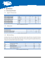
Table 3-1: Digital IO characteristics
3.1.2
Analog Inputs
Parameter
Resolution
Conversion Current
Conversion Core Input Voltage
Conversion Time Per Channel
Symbol
Min
Ic
Vin
tc
0
Typ.
10
1
-
Max
2.4
10
Unit
Bit
mA
V
µs
Table 3-2: ADC characteristics
3.1.3
Maximum Ratings
Stressing the device above the rating listed in the absolute maximum ratings table may cause permanent damage
to the device. These are stress ratings only. Operation of the device at these or any other conditions greater than
those indicated in the operating sections of this specification is not implied. Exposure to absolute maximum rating
conditions for extended periods may affect device reliability.
Symbol
VIO
VLED
IOH /IOL
TAMB
TSTO
TSLD
φAMB
Parameter
Input or output voltage
Backlight supply voltage
Current per pin
Ambient temperature
Storage temperature
Solder temperature for 10 seconds
Relative ambient humidity
Min
-0.5
0
0
-20
-55
Max
3.6
20
10
70
100
260
90
Unit
V
V
mA
°C
°C
°C
%
Table 3-3: Absolute maximum ratings
EXT-SBC-i.MX51-DISP_HUM_V1.2.docx
13