Download Hardware User Manual
Transcript
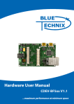
Hardware User Manual
DEV-i.MX53 V1.x
Contact
Bluetechnix Mechatronische Systeme GmbH
Waidhausenstraße 3/19
A-1140 Vienna
AUSTRIA/EUROPE
[email protected]
http://www.bluetechnix.com
Document No.: 100-4120-1.2
Date: 2012-02-14
Preliminary_DEV-i.MX53_HUM_V1.2.docx
2
Table of Contents
i.MX Core Modules..................................................................................................................................................................................... 6
i.MX Development Boards ...................................................................................................................................................................... 8
1
Introduction ....................................................................................................................................................................................... 9
1.1
Overview .................................................................................................................................................................................... 9
1.2
Available extensions ...........................................................................................................................................................10
1.3
Key Features ...........................................................................................................................................................................10
1.3.1
Core Modules ...............................................................................................................................................................10
1.3.2
Active Components on DEV-i.MX53....................................................................................................................10
1.3.3
Optional Parts on DEV-i.MX53 ...............................................................................................................................10
1.4
2
General Description ......................................................................................................................................................................12
2.1
3
4
Applications............................................................................................................................................................................10
Functional Description .......................................................................................................................................................12
2.1.1
Interface Interconnection........................................................................................................................................13
2.1.2
Powering ........................................................................................................................................................................13
2.1.3
Audio ...............................................................................................................................................................................13
2.1.4
HDMI ................................................................................................................................................................................14
2.1.5
JTAG .................................................................................................................................................................................14
2.1.6
USB/UART Bridge ........................................................................................................................................................14
2.1.7
USB ...................................................................................................................................................................................14
2.1.8
USB-OTG.........................................................................................................................................................................14
2.1.9
SDHC-Card.....................................................................................................................................................................14
2.1.10
SATA ................................................................................................................................................................................14
2.1.11
Ethernet ..........................................................................................................................................................................14
2.1.12
ISM Interface .................................................................................................................................................................14
2.1.13
CAN* ................................................................................................................................................................................15
2.1.14
LED Driver ......................................................................................................................................................................15
2.1.15
ADC ..................................................................................................................................................................................15
2.1.16
Acceleration Sensor ...................................................................................................................................................15
2.2
PCB Placement ......................................................................................................................................................................16
2.3
Mechanical Outline ..............................................................................................................................................................16
Specifications...................................................................................................................................................................................19
3.1
Operating Conditions .........................................................................................................................................................19
3.2
Maximum Ratings ................................................................................................................................................................19
3.3
Analog Inputs.........................................................................................................................................................................19
3.4
ESD Sensitivity .......................................................................................................................................................................19
Connector Description .................................................................................................................................................................20
Preliminary_DEV-i.MX53_HUM_V1.2.docx
3
4.1
Digital Video Extension Connector (X22) ....................................................................................................................20
4.1.1
Camera Sensor Interface Port (CSI0) ...................................................................................................................20
4.1.2
LCD Port (DISP0)..........................................................................................................................................................20
4.1.3
Pin Description Table ................................................................................................................................................20
4.2
GPIO/Automation Extension Connector (X23) .........................................................................................................22
4.2.1
Pin Description Table ................................................................................................................................................23
4.3
Image Sensor Connector X21 (BLT-ISM-Connector) ...............................................................................................26
4.4
Reset / Power-On Connector (X10)................................................................................................................................26
4.5
Auxiliary Power Supply Connector (X5).......................................................................................................................27
5
Switches, Jumpers and LEDs .....................................................................................................................................................28
5.1
RGB LED (V12) ........................................................................................................................................................................28
5.2
Push Buttons (S4, S3) ..........................................................................................................................................................28
5.3
Backup Battery (optional) .................................................................................................................................................28
5.4
Board Configuration Switches (S2, S1) .........................................................................................................................28
6
Support ..............................................................................................................................................................................................30
6.1
General Support....................................................................................................................................................................30
6.2
Board Support Packages ...................................................................................................................................................30
6.3
i.MX Software Support .......................................................................................................................................................30
6.3.1
Linux ................................................................................................................................................................................30
6.3.2
Win CE .............................................................................................................................................................................30
6.4
i.MX® Design Services ..........................................................................................................................................................30
6.4.1
7
Upcoming Products and Software Releases ....................................................................................................30
Ordering Information ...................................................................................................................................................................31
7.1
8
Predefined mounting options for DEV-i.MX53 .........................................................................................................31
Dependability ..................................................................................................................................................................................32
8.1
9
MTBF ..........................................................................................................................................................................................32
Product History ...............................................................................................................................................................................33
9.1
Version Information.............................................................................................................................................................33
9.2
Anomalies................................................................................................................................................................................33
10
Document Revision History ...................................................................................................................................................34
11
List of Abbreviations ................................................................................................................................................................35
A
List of Figures and Tables............................................................................................................................................................37
Preliminary_DEV-i.MX53_HUM_V1.2.docx
4
© Bluetechnix Mechatronische Systeme GmbH 2012
All Rights Reserved.
The information herein is given to describe certain components and shall not be considered as a guarantee of
characteristics.
Terms of delivery and rights of technical change reserved.
We hereby disclaim any warranties, including but not limited to warranties of non-infringement, regarding circuits,
descriptions and charts stated herein.
Bluetechnix makes and you receive no warranties or conditions, express, implied, statutory or in any
communication with you. Bluetechnix specifically disclaims any implied warranty of merchantability or fitness for a
particular purpose.
Bluetechnix takes no liability for any damages and errors causing of the usage of this board. The user of this board is
responsible by himself for the functionality of his application. He is allowed to use the board only if he has the
qualification. More information is found in the General Terms and Conditions (AGB).
Information
For further information on technology, delivery terms and conditions and prices please contact Bluetechnix
(http://www.bluetechnix.com).
Warning
Due to technical requirements components may contain dangerous substances.
Preliminary_DEV-i.MX53_HUM_V1.2.docx
5
i.MX Core Modules
CM-i.MX27-C-C-Q26S128F32N512
The Core Module CM-i.MX27 is powered by Freescales' SoC i.MX27 (ARM 926 core, up to 400MHz). It addresses
128MB DDR-RAM, has an onboard NOR-flash of 32MByte and a NAND-flash with 512MByte at a size of 55x45mm.
CM-i.MX31-C-C-Q26S128F40N128-E
The Core Module CM-i.MX31 is powered by Freescales' SoC i.MX31 (ARM1136JF-S core, up to 532MHz). It
addresses 128MB DDR-RAM, has an onboard NOR-flash of 40MByte and a NAND-flash with 128MByte at a size of
55x45mm. Core module is available as connector or BGA.
CM-i.MX53-C-I-Q24S1024F4N2048)
The Core Module CM-i.MX53 is powered by Freescales' SoC i.MX53 (ARM® Cortex™-A8, up to 1GHz). It addresses
1024MB DDR2-SDRAM, has an onboard NOR-flash of 4MByte and a NAND-flash with 2048MByte at a size of
80x45mm.
Preliminary_DEV-i.MX53_HUM_V1.2.docx
6
Core Module naming information
The idea is to put more Core Module specific technical information into the product name. New Core Module names
will have following technical information covered in their names.
•
Product Family,
•
CPU-Type,
•
Connection-Type,
•
Operating Temperature Range,
•
Crystal Frequency [MHz],
•
RAM [MB],
•
Flash [MB],
•
External Controllers
•
Optional
o
Special and/or
o
Former name
That expands of course the name but allows the customer to get the most important Core Module specific
information at the first sight. Have a look at the example below to get an idea of the new Core Module names.
Example CM-BF537-C-C-Q25S32F4 (CM-BF537E)
CM - BF537 - C - C - Q25
S32
F4 -
-
(CM-BF537E)
Product Family
Former name
CM = Core Module
Special
SBC = Single Board Computer
Custom Core Modules or specials
CPU-Type
uC = uclinux
Equals the name of CPU
Extra controllers mounted
Connection-Type
E = Ethernet
A = BGA
U = USB
B = Border pad
Flash [MB]
C = Connector
F = NOR Flash [MB]
S = SSpecial
N = NAND Flash [MB]
Operating Temperature Range
RAM
A = Automotive
(-40° to +125°)
S = SDRAM [MB]
C = Commercial
(0° to +70°)
I = Industry
(-40° to +85°)
Crystal Frequency
Notation: QXX[MHz]
Preliminary_DEV-i.MX53_HUM_V1.2.docx
7
i.MX Development Boards
DEV-i.MX27
The DEV-i.MX27 development board is an extendable development platform for the CM-i.MX27 processor modules.
With display connector and keypad it can be used as a reference design for a low power mobile handheld device
powered by a single Lithium Ion battery. The development board provides all interfaces of the connector version on
dedicated expansion connectors. Extender boards can be plugged on top of the development board in order to
enable additional interfaces.
DEV-iMX31
The DEV-i.MX31 Development Board is an extendable development platform for the CM-i.MX31 processor module.
With display connector and keypad it can be used as a reference design for a low power mobile handheld device
powered by a single Lithium Ion battery. The development board provides all interfaces of the connector version on
dedicated expansion connectors. Extender boards can be plugged on top of the development board in order to
enable additional interfaces.
SBC-i.MX51-S-C-Q24S512N2048
The Single-Board Computer SBC-i.MX51 is based on Freescale’s high-performance i.MX51 mobile platform,
incorporating an ARM Cortex-A8 CPU, an Image Processing Unit (IPUv3EX), a Video Processing Unit (VPU) and a
Graphical Processing Unit (GPU). The IPUv3EX provides comprehensive support for connectivity to displays and
cameras. The VPU supports hardware encoding and decoding of MPEG-4, H.263, H.264 and many more standards.
The GPU serves 3D and 2Dacceleration in hardware. The board‘s memory capabilities (NAND Flash, DDR2) and
numerous interfaces like Ethernet, HDMI,4xUSB and USB-OTG turn the SBC-i.MX51 into the ultimate development
board for future high-end embedded devices.
DEV-i.MX53
The DEV-i.MX53 development board is an extendable development platform for the CM-i.MX53 processor module.
The development board provides all interfaces of the connector version (Ethernet, HDMI,4xUSB and USB-OTG) on
dedicated extender connectors. Extender boards can be plugged on top of the development board in order to
enable additional interfaces.
Extender boards
Extender boards (EXT-SBC-i.MX51-) are expanding the development board SBC-i.MX51 by several interfaces and
functionalities. Targeted application areas are: audio/video processing, security and surveillance, Ethernet access,
positioning, automation and control, experimental development and measuring.
Note! Bluetechnix is offering tailored board developments as well.
Preliminary_DEV-i.MX53_HUM_V1.2.docx
8
1 Introduction
The DEV-i.MX53 Development Board is a feature rich, low cost rapid development platform designed to decrease
time-to-market of customized applications. It supports Bluetechnix’ powerful i.MX53 based Core Module. The
development board provides all interfaces on dedicated connectors and features the latest extender socket
(bottom side) for upcoming extender boards. The form factor of the DEV-i.M5x allows easy integration of the board
into OEM products.
In combination with any of Bluetechnix’ CM-i.MX53 the DEV-i.MX53 is a future proof embedded development
platform for high sophisticated applications in all areas!
Target applications include industrial automation and control systems as well as applications making use of the
extensive video features.
Overview
HDMI
4 x USB-A
Mini-USB-B
USB-OTG
JTAG
HDMI
Transmitter
USB-HUB
UART-USB
Bridge
RJ45
CAN i/f
CAN
Video Extender
SATA
Serial I/O Extender
1.1
CM-i.MX53
1-Wire / I2C
Speaker-Out
3-axis
Accelerometer
Mic-In
On-Board Mic
RGB-LED
Driver
Reset Button,
Power On Button
DC-Plug
Line-In
Headphone-Out
RGB LED
SDHC Card Slot
Camera
Interface
Core Module
Active
Components
User Interfaces
Connectors
Figure 1-1: Overview of the main components
Preliminary_DEV-i.MX53_HUM_V1.2.docx
9
1.2
Available extensions
In addition, different extensions boards from Bluetechnix are available. Further boards are added based on the
number of customer demands. All specifications you need to design a custom board of your own are freely available
so you can start your design right away. Bluetechnix also offers design support for your custom extensions. The
following extensions are currently planned and will be available soon.
•
•
1.3
EXT-i.MX53-COMM
o GPS
o GSM
o UMTS
o Bluetooth/WLAN
o Display Interface for TFT Displays with RGB interface
o Two Display Interfaces for TFT Displays with LVDS interface
o Image Sensor Interface
EXT-i.MX53-EXP
o Experimental board making every pin on the extension board available on a test point (allows for
rapid prototyping)
Key Features
1.3.1
Core Modules
The DEV-i.MX53 allows the use of i.MX Core Modules based on the i.MX53 processor family.
1.3.2
•
•
•
•
•
•
•
1.3.3
•
•
•
Active Components on DEV-i.MX53
HDMI/DVI Transmitter (Analog Devices AD9889)
7 Port USB HUB (SMSC USB2517)
DC-DC Converters (5.0V: LM3485; 3.3V: ADP2301; 1.8V: ADP2108)
USB/UART Bridge (Silicon Labs CP2104)
CAN Transceiver (TI SN65HVD232D)
RGB-LED driver with I²C interface (Toshiba TCA62724FMG)
4 Channel ADC (AD7993) for voltage monitoring or resistive touch panels
Optional Parts on DEV-i.MX53
On-board microphone (Knowles Acoustics SPM0208HD5)
Acceleration sensor (Freescale MMA7660FCR1)
2x 2.5W Audio Amp (ON-Semi NCP2820FCT2G)
Please understand that these are only active parts and require additional connectors and passive parts as well. We
provide information regarding these parts on request.
1.4
Applications
•
Automotive infotainment
•
Single Board Computer
•
Tablets
Preliminary_DEV-i.MX53_HUM_V1.2.docx
10
•
Smart Mobile Devices
•
Human-Machine-Interface
•
Medical Devices
•
Video Conference Systems
•
Imaging and Consumer Multimedia
•
Set Top Boxes
•
Video Conference Applications
•
Portable Media Players
•
Industrial Applications
•
High-end Mobile Internet Devices (MID), High-end PDAs
•
Netbooks (web tablets)
•
Nettops (internet desktop devices)
•
High-end portable media players (PMP) with HD video capability
•
Portable navigation devices (PND)
Preliminary_DEV-i.MX53_HUM_V1.2.docx
11
2 General Description
The DEV-i.MX53 is a development board for i.MX Core Modules based on the ARM Cortex A8™ core (CM-i.MX53). The
development board features a broad spread selection of available interfaces from the Core Module, like USB,
USBOTG, Ethernet, SATA, SD-Card, HDMI, CAN*, and analog audio. In addition there is the possibility to access
unused interfaces by applying an extension board to the extension connectors located on the bottom side.
* Available only for Industrial Core Modules (see chapter 7).
2.1
Functional Description
Figure 2-1 shows the on-board components and how they are connected to the Core Module. A more precise listing
including which interface is routed to which board extension connectors is shown in the interconnection tables
below.
USB-OTG
SATA
Reset Button,
Power On Button
RJ45
DC/DC
Regulators
DC-Plug
USBH2
USB-HUB
4 x USB-A
Bootmode
Switches
SATA
Camera
Interface
CSI0
UART1
UART-USB
Bridge
Mini-USB-B
SDHC Card Slot
SD3
DISP1
HDMI
Transmitter
HDMI
CAN1
CAN i/f
CAN
I²C2
RGB-LED
Driver
Power LED,
RGB LED
2.5W Audio
Amp
Speaker-Out
LAN
USBOTG
CM-i.MX53
14-pin 2.54mm
Header
JTAG
I²C2
3-axis
Accelerometer
4 Channel ADC
Audio Interface
Video Extender
Serial I/O Extender
Line-In
Core Module
Headphone-Out
Active
Components
Mic-In
User Interfaces
On-Board Mic
Connectors
CM Interfaces
Figure 2-1: DEV-i.MX53 Interconnection Diagram
Preliminary_DEV-i.MX53_HUM_V1.2.docx
12
2.1.1
Interface Interconnection
The following table lists all available interfaces from the Core Module and how they are interconnected on the
Development Board.
Interface
AUDIO
AUD5
CAN1
eCSPI1
eCSPI2
eSDHC2
eSDHC3
FIRI
CSI0
DI0
DI1
LAN
LVDS0
LVDS1
OWIRE
PWM
I²C2
Category
Analog Audio
Digital Audio
CAN
SPI
SPI
SD-Card
SD-Card
UART (IrDA)
IPU
IPU
IPU
Ethernet
LDB
LDB
OWIRE
PWM
I²C
Pins
8
6
2
5
5
11
6
2
14
21
27
6
10
10
1
2
2
I²C3
SATA
UART1
UART2
UART3
USBOTG
USBH1
I²C
SATA
UART
UART
UART
USB
USB
2
4
2
4
4
2
2
Connected to
Triple 3.5mm Audio Jack
HDMI Transmitter
CAN Transceiver
Extension Connector
Extension Connector
Extension Connector
SD-Card
Extension Connector
BLT-ISM interface; Extension Connector
Extension Connector
HDMI Transceiver
RJ45 Socket
Extension Connector
Extension Connector
Extension Connector
Extension Connector
RGB-LED Driver, Acceleration Sensor, HDMI
Transmitter, Extension Connector
Extension Connector
Serial ATA Connector
UART-USB Bridge
Extension Connector
Extension Connector
Mini USB-AB Connector
USB Hub
Comment
SS0 + SS1
SS0 + SS1
8-bit
4-bit
2-bit
10-bit
18-bit
24-bit
Pull-Ups on Board
No Pull-Ups
Supply for 2.5” HDD
Table 2-1: CM-i.MX53 Interface routing
2.1.2
Powering
The DEV-i.MX53 works with a single power supply of 12V to 16V. This input voltage is also routed to the extension
connectors and can be used there, e.g. for TFT backlight etc.
If stand-alone operation is desired, an auxiliary plug provides the option to connect a Li-Ion battery pack with an
external battery charger.
2.1.3
Audio
The audio interface is used to deliver a standard PC audio interface with Microphone-In, Line-In and Line-Out.
Standard 3,5mm audio jacks are used. A Headset can be connected to the Microphone-In and Line-Out connectors.
On request there is the possibility to mount two 2.5W amps. The speakers can be applied to the screw-less terminal
connectors X18 and X19.
On request an on-board microphone can be mounted next to the audio jacks.
Preliminary_DEV-i.MX53_HUM_V1.2.docx
13
2.1.4
HDMI
The HDMI connector provides a standard interface for digital video and audio signals. The HDMI/DVI transmitter is
preprocessing the video signal from the IPU. The audio stream comes from the AUD5 interface of the i.MX53x. The
device can be accessed via the I²C1 bus with the device address 0x39.
2.1.5
JTAG
A standard ARM JTAG connector (20 pins, 2.54mm pitch) is available for processor debugging.
2.1.6
USB/UART Bridge
The UART1 is connected to a SiLabs CP210x, which implements the USB to UART Bridge. A mini USB-B connector is
connected to the device.
2.1.7
USB
The USBH1 port of the DEV-i.MX53 is connected to a seven port USB HUB (SMSC USB2517). Consequently the board
features four standard USB-A connectors, three USB lanes are routed to the IO-extension connector.
2.1.8
USB-OTG
The i.MX53’ internal USB-OTG PHY is routed to a mini USB-A/B connector.
2.1.9
SDHC-Card
The SDHC-Card signals are directly connected to the SD3 port of the CM-i.MX53. A standard SD-Card connector
mounted on the bottom side of the board supports SD and SDHC cards.
2.1.10 SATA
The DEV-i.MX53 allows connecting one SATA HDD or SSD. The 5.0V supply which is needed for most 2.5” HDDs or
SSDs is available on the screw-less terminal connector X25. If a 3.5” HDD is needed, the power supply has to be
realized externally.
The user has to make sure, that no more than 500mA will be drawn from the 5.0V terminal. A 1A fuse is populated
on the DEV-board.
2.1.11 Ethernet
As the Ethernet PHY is already integrated on the Core Module, the LAN signals are routed directly to a RJ45 LAN
connector.
2.1.12 ISM Interface
The camera sensor interface signals (CSI0) are routed to a 30 pin ZIF connector. The connector is compatible to the
Bluetechnix ISM interface and allows connecting all available Image Sensor Modules from Bluetechnix.
Preliminary_DEV-i.MX53_HUM_V1.2.docx
14
2.1.13 CAN*
A SN65HVD232D CAN transceiver is present on the Development Board, which allows integrating the board into a
CAN bus infrastructure. A termination resistor is designed-in, but not populated. If the termination is needed, a
120Ω 0402 SMD resistor can be soldered.
* Available only for Industrial Core Modules (see chapter 7).
2.1.14 LED Driver
A RGB LED is mounted for status signaling. The LED is connected to a TCA62724FMG I²C RGB LED driver. The device
can be accessed via the I²C1 bus with the device address 0x55.
2.1.15 ADC
The AD7993 analog to digital converter has two possible functions. By default it can be used for battery supervisory
to measure battery voltage and charging current. If the battery charger won’t be used, the four channels are
available on the extension connectors and it is possible to connect them to a touch screen panel. The device can be
accessed via the I²C1 bus with the device address 0x22.
2.1.16 Acceleration Sensor
The on-board 3-axis acceleration sensor MMA7660FC is connected to the I²C2 bus and is accessible via address
0x4C.
Preliminary_DEV-i.MX53_HUM_V1.2.docx
15
2.2
PCB Placement
Figure 2-2: Top connectors placement
2.3
Mechanical Outline
This section shows the position of all connectors and mounting holes. All dimensions are given in mm.
Preliminary_DEV-i.MX53_HUM_V1.2.docx
16
Figure 2-3: DEV-i.MX53 top view
Preliminary_DEV-i.MX53_HUM_V1.2.docx
17
Figure 2-4: DEV-i.MX53 bottom view
Preliminary_DEV-i.MX53_HUM_V1.2.docx
18
3 Specifications
3.1
Operating Conditions
Symbol
VIN
P
VUSBx
IUSBx
Parameter
Input supply voltage
Board Power Consumption1)
USB Supply Voltage
USB Supply Current
Min
12
Typical
12
TBD
5.0
-
4.5
-
Max
16
TBD
5.5
500
Unit
V
W
V
mA
Table 3-1: Electrical characteristics
The Power consumption refers to a CM-i.MX53 with Android running in idle state and no Extension Boards or USBDevices plugged in.
1)
3.2
Maximum Ratings
Stressing the device above the rating listed in the absolute maximum ratings table may cause permanent damage
to the device. These are stress ratings only. Operation of the device at these or any other conditions greater than
those indicated in the operating sections of this specification is not implied. Exposure to absolute maximum rating
conditions for extended periods may affect device reliability.
Symbol
VIO
VIN
IOH /IOL
TAMB
TSTO
φAMB
Parameter
Input or output voltage
Input supply voltage
Current per pin
Ambient temperature
Storage temperature
Relative ambient humidity
Min
-0.5
TBD
0
-40
-55
Max
3.6
TBD
10
85
150
90
Unit
V
V
mA
°C
°C
%
Table 3-2: Absolute maximum ratings
3.3
Analog Inputs
The 10-bit ADC, which is integrated in the AD7993BRUZ-0, allows measuring analog voltages. These analog inputs
are mainly used for resistive touchpad sensing or voltage (battery) monitoring.
Parameter
Resolution
Conversion Core Input Voltage
Conversion Time Per Channel
Symbol
Min
Vin
tc
0
Typ.
10
-
Max
3.3
2
Unit
Bit
V
µs
Table 3-3: ADC characteristics
3.4
ESD Sensitivity
ESD (electrostatic discharge) sensitive device.
Charged devices and circuit boards can discharge without detection. Although this
product features patented or proprietary protection circuitry, damage may occur on
devices subjected to high energy ESD. Therefore, proper ESD precautions should be taken
to avoid performance degradation or loss of functionality.
Preliminary_DEV-i.MX53_HUM_V1.2.docx
19
4 Connector Description
4.1
Digital Video Extension Connector (X22)
The video extension connector allows customers to design their own video extension with user-defined camera and
display components. A 100-pin-0.5mm-pitch mezzanine connector FX-10A-100S/10SV_M from Hirose (mating part is
FX10A-100P/10-SV) is used.
4.1.1
Camera Sensor Interface Port (CSI0)
A camera or an alternative video device (such as the OV2655 or the ADV7180) can be connected to the DEV-i.MX53
board using the CMOS Sensor Interface 0 (CSI0).
Width (bit)
10
5
2
14
Interface
CSI0
CSI0
I2C1
Power
Description
CSI0.D0 – CSI0.D9
CSI0.VSYNC, CSI0.HSYNC, CSI0.VSYNC, CSI0.PCLK, CSI0.DE
I2C1.SDA, I2C1.SCL - Camera control interface
3V3, P_SW3_2V5, 5V0, VIN, GND
Table 4-1: CSI port overview
4.1.2
LCD Port (DISP0)
The DISP0 interface is available to connect an LCD display and a touch screen to the DEV-i.MX53 board. The i.MX53
supports display resolutions up to 1680X1050 (WSXGA+).
Width (bit)
16
4
1
10
10
15
Interface
DISP0
DISP0
PWM
LVDS1
LVDS0
Power
Description
DISP0.D0 – DISP0.D17
DISP0.VSYNC, DISP0.HSYNC, DISP0.CLK, DISP0.DE
CRTL.PWM2
LVDS1 interface
LVDS0 interface
3V3, P_SW3_2V5, 5V0, VIN, GND
Table 4-2: LCD port overview
4.1.3 Pin Description Table
Pin No
1
2
3
4
5
6
7
8
9
10
11
12
13
Signal
GND
GND
GND
5V0
5V0
DISP0.D1
DISP0.D3
DISP0.D5
DISP0.D7
GND
DISP0.D9
DISP0.D11
DISP0.D13
Type
PWR
PWR
PWR
PWR
PWR
O
O
O
O
PWR
O
O
O
Preliminary_DEV-i.MX53_HUM_V1.2.docx
Description
Power Ground
Power Ground
Power Ground
Power Supply
Power Supply
Display Port 0 Data
Display Port 0 Data
Display Port 0 Data
Display Port 0 Data
Power Ground
Power Ground
Display Port 0 Data
Display Port 0 Data
20
Pin No
14
15
16
17
18
19
20
21
22
23
24
25
26
27
28
29
30
31
32
33
34
35
36
37
38
39
40
41
42
43
44
45
46
47
48
49
50
51
52
53
54
55
56
57
58
59
60
61
62
63
64
65
66
Signal
DISP0.D15
DISP0.D17
GND
DISP0.CLK
GND
CSI0_D10
CSI0_D10
CSI0_D10
CSI0_D10
CSI0_D10
CSI0_D10
CSI0_D10
CSI0_D10
CSI0_D10
CSI0_D10
GND
CSI0_DE
GND
CSI0_PCLK
GND
CSI0_HSYNC
CSI0_VSYNC
LVDS1.CLK_N
LVDS1.CLK_P
LVDS1.TX0_N
LVDS1.TX0_P
LVDS1.TX1_N
LVDS1.TX1_P
LVDS1.TX2_N
LVDS1.TX2_P
LVDS1.TX3_N
LVDS1.TX3_P
P_SW3_2V5
P_SW3_2V5
GND
GND
GND
GND
GND
GND
3V3
3V3
LVDS0.TX3_P
LVDS0.TX3_N
LVDS0.TX2_P
LVDS0.TX2_N
LVDS0.TX1_P
LVDS0.TX1_N
LVDS0.TX0_P
LVDS0.TX0_N
LVDS0.CLK_P
LVDS0.CLK_N
GPIO4_1
Type
O
O
PWR
O
PWR
IO
IO
IO
IO
IO
IO
IO
IO
IO
IO
PWR
O
PWR
I
PWR
I
I
IO
IO
O
O
O
O
O
O
O
O
PWR
PWR
PWR
PWR
PWR
PWR
PWR
PWR
PWR
PWR
O
O
O
O
O
O
O
O
IO
IO
IO
Preliminary_DEV-i.MX53_HUM_V1.2.docx
Description
Display Port 0 Data
Display Port 0 Data
Power Ground
Display Port 0 Clock
Power Ground
CMOS sensor interface 0 Data
CMOS sensor interface 0 Data
CMOS sensor interface 0 Data
CMOS sensor interface 0 Data
CMOS sensor interface 0 Data
CMOS sensor interface 0 Data
CMOS sensor interface 0 Data
CMOS sensor interface 0 Data
CMOS sensor interface 0 Data
CMOS sensor interface 0 Data
Power Ground
CMOS sensor interface 0 Data Enable
Power Ground
CMOS sensor interface 0 Pixel Clock
Power Ground
CMOS sensor interface 0 HSYNC
CMOS sensor interface 0 VSYNC
LVDS Clock (-)
LVDS Clock (+)
LVDS Transmit Data0 (-)
LVDS Transmit Data0 (+)
LVDS Transmit Data1 (-)
LVDS Transmit Data1 (+)
LVDS Transmit Data2 (-)
LVDS Transmit Data2 (+)
LVDS Transmit Data3 (-)
LVDS Transmit Data3 (+)
Power Supply
Power Supply
Power Ground
Power Ground
Power Ground
Power Ground
Power Ground
Power Ground
Power Supply
Power Supply
LVDS Transmit Data3 (+)
LVDS Transmit Data3 (-)
LVDS Transmit Data2 (+)
LVDS Transmit Data2 (-)
LVDS Transmit Data1 (+)
LVDS Transmit Data1 (-)
LVDS Transmit Data0 (+)
LVDS Transmit Data0 (-)
LVDS Clock (+)
LVDS Clock (-)
Camera Output Enable
21
Pin No
67
68
69
70
71
72
73
74
75
76
77
78
79
80
81
82
83
84
85
86
87
88
89
90
91
92
93
94
95
96
97
98
99
100
Signal
GPIO4_0
GPIO4_2
VGAGND
RGB.R
VGAGND
RGB.G
VGAGND
RGB.B
VGAGND
NC
I2C1.SCL
I2C1.SDA
NC
CTRL.PWM2
GND
DISP0.DE
DISP0.VSYNC
DISP0.HSYNC
GND
DISP0.D16
DISP0.D14
DISP0.D12
DISP0.D10
DISP0.D8
GND
DISP0.D6
DISP0.D4
DISP0.D2
DISP0.D0
VIN
VIN
GND
GND
GND
Type
O
O
PWR
O
PWR
O
PWR
O
PWR
NC
IO
IO
NC
O
PWR
O
I
I
PWR
O
O
O
O
O
PWR
O
O
O
O
PWR
PWR
PWR
PWR
PWR
Description
Camera Trigger
Global Camera Reset
Power Ground
AV Out Red
Power Ground
AV Out Green
Power Ground
AV Out Black
Power Ground
Not Connected
I2C Clock
I2C Data
Not Connected
PWM
Power Ground
Display Port 0 Data Enable
Display Port 0 Data VSYNC
Display Port 0 Data HSYNC
Power Ground
Display Port 0 Data
Display Port 0 Data
Display Port 0 Data
Display Port 0 Data
Display Port 0 Data
Power Ground
Display Port 0 Data
Display Port 0 Data
Display Port 0 Data
Display Port 0 Data
Power Supply
Power Supply
Power Ground
Power Ground
Power Ground
Table 4-3: Digital video extension connector (X22) pin description
4.2
GPIO/Automation Extension Connector (X23)
The GPIO / automation extension connector allow customers to design their own GPIO extension with user-defined
components. A 100-pin-0.5-pitch mezzanine connector (FX-10A-100S/10SV_M from Hirose (mating part is FX10A100P/10-SV) is used. Many interfaces have alternate functions and can also be used as GPIOs.
Interface
1-Wire
Analog-In
I2C
PWM
SD
SPI
Width (bit)
1
4
2
2
12
10
Interface
OWIRE
ADIN
I2C3
PWM1, PWM2
SD2
ECSPI1, ECSPI2
Preliminary_DEV-i.MX53_HUM_V1.2.docx
Description
OWIRE
ADIN[1..4]
I2C3.SCL, I2C3.SDA
PWM1, PWM2
SD2.CMD, SD2.CLK, SD2.WP, SD2.CD. SD2.D0 – SD2.D7
ECSPI1.MOSI, ECSPI1.MISO,
ECSPI1.SS0, ECSPI1.SS1, ECSPI1.SCLK
ECSPI2.MOSI, ECSPI2.MISO,
ECSPI2.SS0, ECSPI2.SS1, ECSPI2.SCLK
22
Interface
UART
Width (bit)
8
Interface
UART2, UART3
CAN
USB
2
12
FIRI
Power
2
35
CAN1
USBH5,
USBH6,
USBH7
FIRI
Description
UART2.TXD, UART2.RXD, UART2.RTS, UART2.CTS
UART3.TXD, UART3.RXD, , UART3.RTS, UART3.CTS
CAN1.RXD, CAN1.TXD
USBH5.D_P, USBH5.D_N, USBH5.PWR, USBH5.OC
USBH6.D_P, USBH6.D_N, USBH6.PWR, USBH6.OC
USBH7.D_P, USBH7.D_N, USBH7.PWR, USBH7.OC
FIRI.RXD, FIRI.TXD
5V0, VIN, VUSB5, P_SW3_2V5, 3V3, P_LDO4_2V8, GND
Table 4-4: GPIO / automation extension connector (X23) port overview
4.2.1 Pin Description Table
Pin No
1
2
3
4
5
6
7
8
9
10
11
12
13
14
15
16
17
18
19
20
21
22
23
24
25
26
27
28
29
30
31
32
33
34
35
36
Signal
GND
GND
GND
5V0
5V0
USBH7.D_P
USBH7.D_N
USBH7.PWR
USBH7.OC
GND
I2C3.SCL
I2C3.SDA
OWIRE
VUSB5
VUSB5
CAN1.RXD
CAN1.TXD
P_LDO4_2V8
GPIO.(2V8)_3
GPIO.(2V8)_4
GND
UART2.RXD
UART2.TXD
UART2.RTS
UART2.CTS
GND
UART3.RXD
UART3.TXD
UART3.RTS
UART3.CTS
FIRI.RXD
FIRI.TXD
GND
NC
CTRL.PWM1
CTRL.PWM2
Type
PWR
PWR
PWR
PWR
PWR
IO
IO
O
I
PWR
O
IO
IO
PWR
PWR
I
O
PWR
IO
IO
PWR
I
O
O
I
PWR
I
O
O
I
O
I
PWR
NC
O
O
Preliminary_DEV-i.MX53_HUM_V1.2.docx
Description
Power Ground
Power Ground
Power Ground
Power Supply
Power Supply
USB Data+
USB DataUSB Power Enable
USB Over Current
Power Ground
I2C Clock
I2C Data
One Wire Interface
500mA Current Limited 5V Power Supply for USB Host 5
500mA Current Limited 5V Power Supply for USB Host 5
CAN Receive Data / GPIO4_11
CAN Transmit Data / GPIO4_10
Power Supply
GPIO4_3
GPIO4_4
Power Ground
UART Receive Data
UART Transmit Data
UART Request To Send
UART Clear To Send
Power Ground
UART Receive Data
UART Transmit Data
UART Request To Send
UART Clear To Send
Fast Infrared Interface Receive Data
Fast Infrared Interface Transmit Data
Power Ground
Not Connected
Pulse Width Modulation Output / GPIO1_9
Pulse Width Modulation Output / GPIO1_19
23
Pin No
37
38
39
40
41
42
43
44
45
46
47
48
49
50
51
52
53
54
55
56
57
58
59
60
61
62
63
64
65
66
67
68
69
70
71
72
73
74
75
76
77
78
79
80
81
82
83
84
85
Signal
P_SW3_2V5
NC
GND
ECSPI2.MOSI
ECSPI2.MISO
ECSPI2.SS1
ECSPI2.SS2
NC
ECSPI2.SCLK
3V3
3V3
GND
GND
GND
GND
GND
GND
VIN
VIN
ECSPI1.SCLK
NC
ECSPI1.SS1
ECSPI1.SS0
ECSPI1.MISO
ECSPI1.MOSI
GND
ADIN4
ADIN3
ADIN2
ADIN1
SD2.D7
SD2.D6
SD2.D5
SD2.D4
SD2.D3
SD2.D2
SD2.D1
SD2.D0
GND
SD2.CLK
SD2.CMD
GND
SD2.WP
SD2.CD
P_SW3_2V5
GPIO.(2V5)_3
GPIO.(2V5)_2
GPIO.(2V5)_1
GPIO.(2V5)_0
Type
PWR
NC
PWR
O
I
O
O
NC
O
PWR
PWR
PWR
PWR
PWR
PWR
PWR
PWR
PWR
PWR
O
NC
O
O
I
O
PWR
I
I
I
I
IO
IO
IO
IO
IO
IO
IO
IO
PWR
O
O
PWR
I
I
PWR
IO
IO
IO
IO
Preliminary_DEV-i.MX53_HUM_V1.2.docx
Description
Power Supply
Not Connected
Power Ground
SPI MOSI
SPI MISO
SPI Select1
SPI Select2
Not Connected
SPI CLK
Power Supply
Power Supply
Power Ground
Power Ground
Power Ground
Power Ground
Power Ground
Power Ground
Power Supply
Power Supply
SPI CLK
Not Connected
SPI Select1
SPI Select0
SPI MISO
SPI MOSI
Power Ground
Vin4 (AD7993)
Vin3 (AD7993)
Vin2 (AD7993)
Vin1 (AD7993)
SD Data7 / GPIO2_15
SD Data6 / GPIO2_14
SD Data5 / GPIO2_13
SD Data4 / GPIO2_12
SD Data3 / GPIO1_12
SD Data2 / GPIO1_13
SD Data1 / GPIO1_14
SD Data0 / GPIO1_15
Power Ground
SD Clock / GPIO1_10
SD Command / GPIO1_11
Power Ground
SD Card Detect / GPIO2_31
SD Write Protect / GPIO1_2
Power Supply
GPIO5_13
GPIO1_18
GPIO1_17
GPIO1_16
24
Pin No
86
87
88
89
90
91
92
93
94
95
96
97
98
99
100
Signal
GND
USBH5_OC
USBH5_PWR
USBH5_D_N
USBH5_D_P
GND
USBH6_OC
USBH6_PWR
USBH6_D_N
USBH6_D_P
5V0
5V0
GND
GND
GND
Type
PWR
I
O
IO
IO
PWR
I
O
IO
IO
PWR
PWR
PWR
PWR
PWR
Description
Power Ground
USB Over Current
USB Power Enable
USB DataUSB Data+
Power Ground
USB Over Current
USB Power Enable
USB DataUSB Data+
Power Supply
Power Supply
Power Ground
Power Ground
Power Ground
Table 4-5: GPIO / automation extension connector (X23) pin description
Preliminary_DEV-i.MX53_HUM_V1.2.docx
25
4.3
Image Sensor Connector X21 (BLT-ISM-Connector)
Pin
1
2
3
4
5
6
7
8
9
10
11
12
13
14
15
16
17
18
19
20
21
22
23
24
25
26
27
28
29
30
Name
VCAMA
GND
SADDR
NC
GPIO4_2
I2C1.SCL
I2C1.SDA
VCAMC
GND
CSI0.PCLK
CSI0.VSYNC
CSI0.HSYNC
GPIO4_0
STROBE
NC
NC
CSI0.D0
CSI0.D1
VCAMIO
GND
CSI0.D2
CSI0.D3
CSI0.D4
CSI0.D5
GND
CSI0.D6
CSI0.D7
CSI0.D8
CSI0.D9
CSI0.DE
Type
PWR
PWR
NC
NC
O
O
I/O
PWR
PWR
I
I
I
O
I
NC
NC
I
I
PWR
PWR
I
I
I
I
PWR
I
I
I
I
O
Description
Camera Analog Voltage Supply
Power Ground
Not Connected
Not Connected
Global Camera Reset
Configuration Bus Clock Line
Configuration Bus Data Line
Camera Core Voltage Supply
Power Ground
Pixel Clock
VSYNC
HSYNC
Camera Trigger
Strobe Signal from Camera (available only on solder pad)
Not Connected
Not Connected
Pixel Data
Pixel Data
Camera IO Power Supply
Power Ground
Pixel Data
Pixel Data
Pixel Data
Pixel Data
Power Ground
Pixel Data
Pixel Data
Pixel Data
Pixel Data
Output Enable (Active Low)
Table 4-6: BLT-ISM-Connector interface description (X21)
4.4
Reset / Power-On Connector (X10)
The two signals Power-On and Reset are accessible via this connector. These signals are the same as the ones routed
to the two push buttons.
Pin No
1
2
3
4
Signal
CTRL.ON
GND
CTRL.NRESET_IN
GND
Description
Power On (internally pulled up)
Signal ground
Power On Reset (internally pulled up)
Signal ground
Table 4-7: Reset / power-on connector pin description
Preliminary_DEV-i.MX53_HUM_V1.2.docx
26
4.5
Auxiliary Power Supply Connector (X5)
The auxiliary Power Supply Extension Connector provides the possibility to power the board via a 12-pin Connector
(ERNI 063179). It is possible to connect a supply voltage to the Vin Pins, or to connect an external battery charger.
Pin No
1A
2A
3A
4A
5A
6A
Signal
I²C1.SCL
I²C1.SDA
PWR_GT
GND
CHRG_IN
CHRG_IN
Description
I²C1 Serial Clock
I²C1 Serial Data
Power Gate (for DC Connector)
Power Ground
Power Supply for External Charger
Power Supply for External Charger
Pin No
1B
2B
3B
4B
5B
6B
Signal
GPIO5_13
GPIO1_18
GPIO1_17
GND
Vin
Vin
Description
Free Configurable Control IO
Free Configurable Control IO
Free Configurable Control IO
Power Ground
Dev-Board Power Supply
Dev-Board Power Supply
Table 4-8: Auxiliary power supply extension connector pin description
Preliminary_DEV-i.MX53_HUM_V1.2.docx
27
5 Switches, Jumpers and LEDs
5.1
RGB LED (V12)
The RGB LED is connected to the TCA62724FMG RGB-LED driver and can be used for status signaling.
5.2
Push Buttons (S4, S3)
The push buttons have the following functions:
•
•
5.3
S3: RESET
S4: Power On/Off
Backup Battery (optional)
There is also a possibility to add a 6.8mm non-rechargeable lithium coin cell to keep the RTC running and the RAM
self-refreshing. The DEV/i.MX53 is delivered only on request with a 6.8mm coin cell holder. Bluetechnix does not
provide any batteries due to legal restrictions.
5.4
Board Configuration Switches (S2, S1)
The DEV-i.MX53 supports five different boot modes. For USB/UART boot mode, the i.MX53 is polling for activity on
both USBOTG and UART1. For a more detailed explanation please see the software documentation on
http://support.bluetechnix.at/wiki.
Preliminary_DEV-i.MX53_HUM_V1.2.docx
28
Mode
Switch
Boot Switch Setting
On
Off
S2
1
Boot Media
1 2 3 4 5 6 7 8
On
Off
S1
SPI NOR Flash
1 2 3 4 5 6 7 8
On
Off
S2
2
1 2 3 4 5 6 7 8
On
Off
S1
NAND Flash (Consumer Core Module Version)
1 2 3 4 5 6 7 8
On
Off
S2
3
1 2 3 4 5 6 7 8
On
Off
S1
NAND Flash (Industrial Core Module Version)
1 2 3 4 5 6 7 8
On
Off
S2
4
1 2 3 4 5 6 7 8
On
Off
S1
SD card
1 2 3 4 5 6 7 8
On
Off
S2
5
1 2 3 4 5 6 7 8
On
Off
S1
SATA hard disk
1 2 3 4 5 6 7 8
On
Off
S2
6
1 2 3 4 5 6 7 8
On
Off
S1
USB/UART boot mode
1 2 3 4 5 6 7 8
Table 5-1: Supported Boot Modes
Preliminary_DEV-i.MX53_HUM_V1.2.docx
29
6 Support
6.1
General Support
General support for products can be found at Bluetechnix’ support site https://support.bluetechnix.at/wiki
6.2
Board Support Packages
Board support packages, boot loaders and further software downloads can be downloaded at the products wiki
page at https://support.bluetechnix.at/wiki
6.3
6.3.1
i.MX Software Support
Linux
Linux BSP and images of derivates can be found at Bluetechnix’ support site https://support.bluetechnix.at/wiki at
the software section of the related product.
6.3.2
Win CE
WinCE is only supported on ARM platforms. Please contact Bluetechnix for support information.
6.4
i.MX® Design Services
Based on more than seven years of experience with Blackfin and i.MX, Bluetechnix offers development assistance as
well as custom design services and software development.
6.4.1
Upcoming Products and Software Releases
Stay up to date with all
at http://www.bluetechnix.com.
product
Preliminary_DEV-i.MX53_HUM_V1.2.docx
changes,
releases
and
software
updates
of
Bluetechnix
30
7 Ordering Information
7.1
Predefined mounting options for DEV-i.MX53
Article Number
100-4120-1
100-1470-2
100-1471-2
100-1472-2-TR
Name
i.MX53 Development Starter Package
CM-i.MX53-C-I-Q24S1024F4N2048
CM-i.MX53-C-C-Q24S1024F4N2048
CM-i.MX53-C-C-Q24S512F4N256
Description
DEV-i.MX5x + CM-i.MX53-C-C-Q24S1024F4N2048
Industrial version
Commercial version
Tape Reel (Commercial version, 50 pcs per reel)
Table 7-1: Ordering information
NOTE:
Custom hard and software developments are available on request! Please contact Bluetechnix
([email protected]) if you are interested in custom hard- and software development.
Preliminary_DEV-i.MX53_HUM_V1.2.docx
31
8 Dependability
8.1
MTBF
Please keep in mind that a part stress analysis would be the only way to obtain significant failure rate results,
because MTBF numbers just represent a statistical approximation of how long a set of devices should last before
failure. Nevertheless, we can calculate an MTBF of the development board using the bill of material. We take all the
components into account. The PCB and solder connections are excluded from this estimation. For test conditions
we assume an ambient temperature of 30°C of all development board components. We use the MTBF Calculator
from ALD (http://www.aldservice.com/) and use the reliability prediction MIL-217F2 Part Stress standard. Please get
in touch with Bluetechnix ([email protected]) if you are interested in the MTBF result.
Preliminary_DEV-i.MX53_HUM_V1.2.docx
32
9 Product History
9.1
Version Information
Version
1.2
Date
2011 11 24
1.1
2011 08 23
9.2
Changes
Battery charger removed.
Coin cell Holder not mounted.
Core Module mounting holes adapted for new modules (Version V2.0 or higher).
Two different extension connectors to prevent reverse connecting of extension
boards.
Optional plug to connect an external Li-Ion battery pack with charger.
Pin out of extension connector X22 changed (Pin 66 from NC to Cam_OE).
First DEV-i.MX53 release
Table 9-1: Overview product changes
Anomalies
Version
1.2
1.1
Date
2011 11 24
2011 10 02
Description
No anomalies reported yet.
Power Supplies for USB Lane 1 and Lane 2 interchanged. Over-current detection
will not work.
Table 9-2: Overview product anomalies
Preliminary_DEV-i.MX53_HUM_V1.2.docx
33
10 Document Revision History
Version
2
1
Date
2011 11 24
2011 09 05
Document Revision
Updates for HWR V1.2
First draft release
Table 10-1: Revision history
Preliminary_DEV-i.MX53_HUM_V1.2.docx
34
11 List of Abbreviations
Abbreviation
ADC
ADIN
AI
CAN
CM
COMM
CSI
DC
DDR
DEV
DI
DISP
EBI
ESD
EXP
FIRI
GPIO
GPS
GSM
HD
HDD
HDMI
I
I/O
I²C
ISM
JTAG
LAN
LiPol
LVDS
MIC
MTBF
NC
O
OEM
OWIRE
PCB
PDA
PWM
PWR
SATA
SD
SDHC
SDRAM
SoC
SPI
SSD
TFT
TISM
TSC
Description
Analog Digital Converter
Analog Data Input
Analog Input
Controller Area Network
Core Module
Communication
Camera Sensor Interface
Direct Current
Double Data Rate
Development Board
Display Interface
Display
External Bus Interface
Electrostatic Discharge
Experimental
Fast Infrared Interface
General Purpose Input Output
Global Positioning System
Global System for Mobile Communications
High Definition
Hard Disk Drive
High-Definition Multimedia Interface
Input
Input/Output
Inter-Integrated Circuit
Image Sensor Module
Joint Test Action Group
Local Area Network
Lithium-Polymer
Low Voltage Differential Signaling
Microphone
Mean Time Between Failure
Not Connected
Output
Original Equipment Manufacturer
One-Wire
Printed Circuit Board
Personal Digital Assistant
Pulse Width Modulation
Power
Serial Advanced Technology Attachment
Secure Digital
Secure Digital High Capacity
Synchronous Dynamic Random Access Memory
System on Chip
Serial Peripheral Interface
Solid State Disk
Thin-Film Transistor
Tiny Image Sensor Module
Touch Screen Controller
Preliminary_DEV-i.MX53_HUM_V1.2.docx
35
UART
UMTS
USB
USBH
USBOTG
WLAN
ZIF
Universal Asynchronous Receiver Transmitter
Universal Mobile Telecommunications System
Universal Serial Bus
Universal Serial Bus Host
USB On The Go
Wireless Local Area Network
Zero Insertion Force
Table 11-1: List of abbreviations
Preliminary_DEV-i.MX53_HUM_V1.2.docx
36
A
List of Figures and Tables
Figures
Figure 1-1: Overview of the main components ...........................................................................................................................................9
Figure 2-1: DEV-i.MX53 Interconnection Diagram ................................................................................................................................... 12
Figure 2-2: Top connectors placement ........................................................................................................................................................ 16
Figure 2-3: DEV-i.MX53 top view..................................................................................................................................................................... 17
Figure 2-4: DEV-i.MX53 bottom view ............................................................................................................................................................ 18
Tables
Table 2-1: CM-i.MX53 Interface routing ....................................................................................................................................................... 13
Table 3-1: Electrical characteristics ................................................................................................................................................................ 19
Table 3-2: Absolute maximum ratings.......................................................................................................................................................... 19
Table 3-3: ADC characteristics .......................................................................................................................................................................... 19
Table 4-1: CSI port overview ............................................................................................................................................................................. 20
Table 4-2: LCD port overview ........................................................................................................................................................................... 20
Table 4-3: Digital video extension connector (X22) pin description................................................................................................. 22
Table 4-4: GPIO / automation extension connector (X23) port overview ....................................................................................... 23
Table 4-5: GPIO / automation extension connector (X23) pin description .................................................................................... 25
Table 4-6: BLT-ISM-Connector interface description (X21) ................................................................................................................... 26
Table 4-7: Reset / power-on connector pin description ........................................................................................................................ 26
Table 4-8: Auxiliary power supply extension connector pin description ....................................................................................... 27
Table 5-1: Supported Boot Modes.................................................................................................................................................................. 29
Table 7-1: Ordering information ..................................................................................................................................................................... 31
Table 9-1: Overview product changes .......................................................................................................................................................... 33
Table 9-2: Overview product anomalies ...................................................................................................................................................... 33
Table 10-1: Revision history .............................................................................................................................................................................. 34
Table 11-1: List of abbreviations ..................................................................................................................................................................... 36
Preliminary_DEV-i.MX53_HUM_V1.2.docx
37


