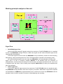
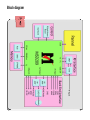
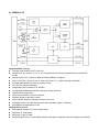
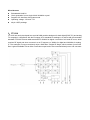
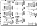
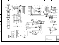
1
FILE NO.
SERVICE MANUAL
LED-46XR10FH(B)
LED-LCD TV
PRODUCT CODE No.
1 682 351 11: PAL-BG(TV) DTV
REFERENCE No.:SM0915178
CONTENTS
Safety precautions………………………………………………………………………..… 3
Alignment instructions …………………………….…….………………………………… 5
Method of software upgrading instructions………………………………………………..13
Working principle analysis of the unit……………………………….………….………….17
Block diagram…………………………………..………………………………….…………19
IC block diagram and instruction…………………………………………………………..……
20
Wiring diagram ……………………………………………………………………………. 29
Troubleshooting guide ………………………………………………………………..…… 30
Schematic diagram………………………………………………………………………… 33
APPENDIX-A: Main assembly list
APPENDIX-B: Exploded View
Installing the Stand or wall-mount bracket
Wall mounting instructions
Attention: This service manual is only for service personnel to take reference with. Before
servicing please read the following points carefully.
Safety precautions
1. Instructions
Be sure to switch off the power supply before replacing or welding any components or
inserting/plugging in connection wire Anti static measures to be taken (throughout the entire
production process!):
a) Do not touch here and there by hand at will;
b) Be sure to use anti static electric iron;
c) It’s a must for the welder to wear anti static gloves.
Please refer to the detailed list before replacing components that have special safety requirements.
Do not change the specs and type at will.
2. Points for attention in servicing of LED
2.1 Screens are different from one model to another and therefore not interchangeable. Be sure to
use the screen of the original model for replacement.
2.2 The operation voltage of LED screen is 700-825V. Be sure to take proper measures in
protecting yourself and the machine when testing the system in the course of normal operation or
right after the power is switched off. Please do not touch the circuit or the metal part of the module
that is in operation mode. Relevant operation is possible only one minute after the power is
switched off.
2.3 Do not use any adapter that is not identical with the TV set. Otherwise it will cause fire or
damage to the set.
2.4 Never operate the set or do any installation work in bad environment such as wet bathroom,
laundry, kitchen, or nearby fire source, heating equipment and devices or exposure to sunlight etc.
Otherwise bad effect will result.
2.5 If any foreign substance such as water, liquid, metal slices or other matters happens to fall into
the module, be sure to cut the power off immediately and do not move anything on the module lest it
should cause fire or electric shock due to contact with the high voltage or short circuit.
2.6 Should there be smoke, abnormal smell or sound from the module, please shut the power off at
once. Likewise, if the screen is not working after the power is on or in the course of operation, the
power must be cut off immediately and no more operation is allowed under the same condition.
2.7 Do not pull out or plug in the connection wire when the module is in operation or just after the
power is off because in this case relatively high voltage still remains in the capacitor of the driving
circuit. Please wait at least one minute before the pulling out or plugging in the connection wire.
2.8 When operating or installing LED please don’t subject the LED components to bending, twisting
or extrusion, collision lest mishap should result.
2.9 As most of the circuitry in LED TV set is composed of CMOS integrated circuits, it’s necessary
to pay attention to anti statics. Before servicing LED TV make sure to take anti static measure and
ensure full grounding for all the parts that have to be grounded.
2.10 There are lots of connection wires between parts behind the LED screen. When servicing or
moving the set please take care not to touch or scratch them. Once they are damaged the screen
would be unable to work and no way to get it repaired.
If the connection wires, connections or components fixed by the thermotropic glue need to
disengage when service, please soak the thermotropic glue into the alcohol and then pull them out
in case of dagmage.
2.11 Special care must be taken in transporting or handling it. Exquisite shock vibration may lead to
breakage of screen glass or damage to driving circuit. Therefore it must be packed in a strong case
before the transportation or handling.
2.12 For the storage make sure to put it in a place where the environment can be controlled so as to
prevent the temperature and humidity from exceeding the limits as specified in the manual. For
prolonged storage, it is necessary to house it in an anti-moisture bag and put them altogether in one
place. The ambient conditions are tabulated as follows:
Temperature
Humidity
Scope for operation
5 ~ +35 oC
Scope for storage
-15~ +45 oC
Scope for operation
20% ~ 80%
Scope for storage
<= 80%
2.13 Display of a fixed picture for a long time may result in appearance of picture residue on the
screen, as commonly called “ghost shadow”. The extent of the residual picture varies with the
maker of LED screen. This phenomenon doesn’t represent failure. This “ghost shadow” may remain
in the picture for a period of time (several minutes). But when operating it please avoid displaying
still picture in high brightness for a long time.
3. Points for attention during installation
3.1 The front panel of LED screen is of glass. When installing it please make sure to put it in place.
3.2 For service or installation it’s necessary to use specified screw lest it should damage the screen.
3.3 Be sure to take anti dust measures. Any foreign substance that happens to fall down between
the screen and the glass will affect the receiving and viewing effect
3.4 When dismantling or mounting the protective partition plate that is used for anti vibration and
insulation please take care to keep it in intactness so as to avoid hidden trouble.
3.5 Be sure to protect the cabinet from damage or scratch during service, dismantling or mounting.
Alignment instructions
1. Safety Instructions
Be sure to switch off the power supply before replacing or welding any components or
inserting/plugging in connection wire Anti static measures to be taken (throughout the entire
production process!):
a) Do not touch here and there by hand at will;
b) Be sure to use anti static electric iron;
c) It’s a must for the welder to wear anti static gloves.
Please refer to the detailed list before replacing components that have special safety requirements.
Do not change the specs and type at will.
2. Test equipment
VG-848 (VGA, YPbPr signal generator)
VG-849 (HDMI digital video signal generator)
CA210 (color analyzer)
3
Alignment flow
3.1 Voltage of power supply test
According to the wiring specified by Product Specification, connect power board, main/data
processing board, IR/light sensor board, key board and backlight board correctly, then switch on main
power and press key “ ” to turn on the TV set.
a) Test each pin voltage of socket X401 (< 26” models) and 13-pin power socket X601 (≥ 26”
models) in turn, please refer voltage of CCFL to Table 1, refer voltage of LED to Table 2:
Table 1
Each pin voltage of 13-pin power socket for CCFL models
1
Pin
1
2
3
4、5
6、7
8
1
9
11
13
0
Vol.
≥2.5 V
≥2.0 V
0
Table 2
12 V±5%
0
N.C.
5 V±5%
0
2
5 V±5%
0
≥2.5 V
Each pin voltage of 13-pin power socket for LED models
Pin
1
2
3
4
5
6
7、8
9、10
11
12
13
Vol/
≥2.5 V
0
5 V±5%
0
5 V±5%
N.C.
0
12 V±5%
0
≥2.0 V
≥2.5 V
b) Test each pin voltage of 5-pin power socket X606 in turn ( ≥ 26” models), please refer voltage
to Table 3:
Table 3
Each pin voltage of 5-pin power socket
Pin
1、2
3、4、5
Vol.
24 V±5%
0
3.2 Alignment flow chart shown as Fig. 1
Check if EDID, HDCP KEY, FLASH have been burned?
Combination alignment for general assembly
White balance alignment
Connect to central signal source, check if TV functions are normal-omitted channel, analog
parameters control, etc.? Check if the output of earphones and speakers are normal?
Input composite AV signal, check if AV functions are normal?
Input component signal YPbPr, check if YPbPr functions are normal?
Input RGB signal, check if display and other functions are normal analog parameters control, H/V center, etc.?
Input digital HDMI signal, check if display and other functions are
normal - analog parameters control, H/V center, etc.?
Insert USB,check its functions.
Other functions checkup, such as LCN, OTA, etc.
Setup before shipment
Accessories checkup and packing
Fig. 1
Alignment flow chart
4
Alignment instructions
4.1 Unit adjustment
4.1.1
According to the wiring specified by Product Specification, connect power board, main/data
processing board, IR/light sensor board, key board and backlight board correctly, then switch on main
power and press key “ ” to turn on the TV set, check if the display is normal.
4.1.2
Using method of factory menu
a)
Press key “SOURCE” first, then press keys “2, 5, 8, 0” in turn to enter into initial factory
menu;
b)
c)
d)
e)
f)
g)
h)
i)
Press keys “▲” and “▼” to move cursor to the item of factory menu;
Press keys “◄” and “►” to change the value when cursor is moved onto one item;
Press key “OK” to enter into the inferior factory menu from current menu page;
Press key “MENU” to exit current menu to its superior factory menu;
Press key “EXIT” to exit factory menu in any case;
Factory menu item: ADC ADJUST, for ADC calibration of RGB and YPBPR;
Factory menu item: W/B ADJUST, for white balance adjustment;
Factory menu item: POWER Mode, for setting power-on mode; the default setting is
“Standby” mode unless specified by customer;
j)
k)
l)
Standby: TV set will be in “standby” mode after power-on;
MEM: TV set will keep states before last power-off;
ForceOn: TV set will turn on automatically; it also can be used as aging mode at factory;
Factory menu item: Other Setting->ISP Mode, the item will not be kept in memory, that is, it
will be always in “OFF” mode after turning on again;
“ON”: Upgrading unit software through D-SUB port while connecting to ISP device;
“OFF”: Normal DDC functions of D-SUB port will recover;
Factory menu item: EEPROM Init, for factory and customer data initialization; TV set will
reset and initial guiding interface will display after executing the item;
Factory menu item: Fac. Channel Preset., for factory channels presetting; it is necessary to
connect to central signal source before operating the item; now digital frequency of central signal
CH28(529.5 MHz)and CH33(564.5 MHz)are distributed to Australia programs DVB-T; original
preset digital programs will not change along with the modification of central signal, so please
operate relevant item of menu “Channel” to search programs;
m) Factory menu item: Shipment, all analog & digital programs for factory adjustment will be
cleared out first, then customer channels will be preset according to order requirements; the item
must be executed before shipment to clear out channels for factory adjustment;
n)
o)
p)
Factory menu item: Other Setting->MST DEBUG, default setting is “OFF”, it will not be kept
in memory, that is, it will always in “OFF” mode after turning on TV set again;
“OFF”: RS232 functions of some engineering machines can match design specifications;
“ON”: It is convenient for design tools to debug the software;
Factory menu item: Backlight, for adjusting brightness of backlight; test voltage of 13-pin
power socket while adjusting the item to make it greater than PWM voltage corresponding to
mixture brightness described by panel specification; the item need not adjustment for it has been
preset by software;
Factory menu item: Other Setting->SSC ADJUST, for expanded spectrum adjustment; the
item need not adjustment for it has been preset by software;
q)
Factory menu item: Other Setting->AUDIO Curve Setting, for sound curve adjustment; if
without special customer requirements, the item need not adjustment commonly for it has been
preset by software;
r)
Factory menu item: Software Update, for software upgrade from USB port; at any channel,
insert USB memory device, select option “YES”, software will auto-search file “MERGE.bin” in
USB memory device to begin upgrade; please execute item “EEPROM Init” before adjustment
again, for old data still remain in E2PROM after software upgrade.
4.1.3 ADC calibration of analog component YPbPr
a) Switch to analog component YPbPr channel;
b)
c)
d)
Press key “SOURCE”, then press keys “2, 5, 8, 0” in turn to enter into initial factory menu;
Move cursor to item “ADC ADJUST” and press key “OK” to enter into inferior factory menu;
Input analog component Y/Pb/Pr signal(VG848 Timing 972(1080i), Pattern 918(8 Color & 16
Grey)); move cursor to item “MODE ”,press keys “▲” and “▼” to select item “YPbPr”,then
move cursor to item “AUTO ADC” and press key “OK” to begin auto-adjustment until prompt
“Success” displays which means successful auto-calibration;
4.1.4 ADC calibration of analog RGB
a) Switch to analog RGB channel;
b)
c)
d)
Press key “SOURCE”, then press keys “2, 5, 8, 0” in turn to enter into initial factory menu;
Move cursor to item “ADC ADJUST” and press key “OK” to enter into inferior factory menu;
Input analog RGB signal(VG848: Timing 856(1024×768/60 Hz), Pattern 914(Color Temp.));
move cursor to item “MODE ”,press keys “▲” and “▼” to select item “RGB”,then move cursor
to item “AUTO ADC” and press key “OK” to begin auto-adjustment until prompt “Success”
displays which means successful auto-calibration.
4.2 White balance adjustment”
Unless specified by customer:
a) < 26” models:
b)
Default color temperature “Cool” is 10000K and its chromatic coordinates is (280, 288); color
temperature “Normal” is 8000K and its chromatic coordinates is (295, 305); color temperature
“Warm” is 6500K and its chromatic coordinates is (323, 329);
≥ 26” models:
Default color temperature “Cool” is 12000K and its chromatic coordinates is (272, 278); color
temperature “Normal” is 9300K and its chromatic coordinates is (285, 293); color temperature
“Warm” is 6500K and its chromatic coordinates is (323, 329);
4.3 Adjustment procedure
TV set should be working over 30 mins to be in stabler state before white balance adjustment; Use
white balance apparatus CA-210 and switch to its BBY channel;
a) Switch to HDMI1channel;
b)
c)
d)
e)
Press key “SOURCE”, then press keys “2, 5, 8, 0” in turn to enter into initial factory menu;
Move cursor to item “W/B ADJUST” and press key “OK” to enter into inferior factory menu;
Input HDMI signal (VG-848 Timing:856(1024×768/60 Hz),Pattern:921(Gray 16 step(H)); move
cursor to item “MODE”, press keys “▲” and “▼” to select item “HDMI1” or other HDMI channels,
then move cursor to item “Temper..” and press keys “▲” and “▼” to select item “Normal”;
Fix item “G-GAIN”, adjust items “R-GAIN, B-GAIN” to set chromatic coordinates of 13th scale as
the value of temperature “Normal”;
f)
g)
h)
i)
j)
k)
l)
Fix item “G-OFFSET”, adjust items “R-OFFSET, B-OFFSET” to set chromatic coordinates of 4th
scale as the value of temperature “Normal”;
During temperature “Normal” adjustment , make sure that chromatic coordinates errors of bright
scale are (x±10, y±15) and chromatic coordinates errors of dark scale are (x±10,y±25);
Move cursor to item “COPY ALL” again to copy data of white balance to other channels;
Check if chromatic coordinates of “Cool” and “Warm” meet the requirements or not, if not, adjust
items “R-GAIN/B-GAIN/R-OFFSET/B-OFFSET” to meet them:
“Cool”: chromatic coordinates errors of bright scale are (x±5, y±15), chromatic coordinates
errors of dark scale are (x±8, y±30);
“Warm”: chromatic coordinates errors of bright & dark scales are both (x±10, y±10);
Check if chromatic coordinates of other channels meet the requirements, if not, adjust them
respectively;
Check white balance of each channel by eye, check if the picture is normal;
Please refer to the adjusting rules as follows:
B Gun:
coordinates of X and Y will increase when B gun is adjusted downwards;
coordinates of X and Y will decrease when B gun is adjusted upwards;
R Gun: adjusting R gun will effect coordinate of X, and value of Lv slightly;
coordinate of X will increase when R gun is adjusted upwards;
coordinate of X will decrease when R gun is adjusted downwards;
G Gun: adjusting G gun will effect coordinate of Y, and value of Lv greatly;
coordinate of Y will increase when G gun is adjusted upwards;
coordinate of Y will decrease when G gun is adjusted downwards.
5
Functions checkup
5.1 Analog & digital TV functions
Input central signal to RF port, enter into menu “CHANNEL”, then search channels automatically,
check if there is any omitted channel, check if the output of speakers and the picture are normal.
5.2 Composite video of AV port
Input composite video signal to AV port, check if the picture and the sound are normal under the
circumstances of power on/off, switching channel and format, etc.
5.3 Analog component YPbPr/YCbCr port
Input analog YPBPR signal from VG848 signal generator with YPBPR formats listed as Table 4
respectively, check if the picture and the sound are normal under the circumstances of power-on/off,
switching channel and format, etc.
Table 4 YPBPR signal formats
No.
Definition
H. - fre.(kHz)
V. – fre.(Hz)
Dot pulse fre.
Note
(MHz)
480i
1
720×480
15.734/15.75
59.94/60
13.5/13.514
2
720×576
15.625
50
13.5
576i (PAL, PAL-N, SECAM)
3
720×480
31.469/31.5
59.94/60
27/27.027
480p
4
720×576
31.25
50
27
576p
5
1280×720
37.5
50
74.25
720p (50p)
6
1280×720
44.955/45
59.94/60
74.176/74.25
720p (59.94p/60p)
(NTSC, NTSC4.43,PAL60,PAL-M)
7
1920×1080
28.125
50
74.25
1080i (50i)
8
1920×1080
33.75
59.94/60
74.176/74.25
1080i (59.94i/60i)
9
1920×1080
26.973
23.976
74.176
1080p (23.97p)
10
1920×1080
27
24
74.25
1080p (24p)
11
1920×1080
28.125
25
74.25
1080p (25p)
12
1920×1080
33.716
29.97
74.176
1080p (29.97p)
13
1920×1080
33.75
30
74.25
1080p (30p)
14
1920×1080
56.25
50
148.5
1080p (50p)
15
1920×1080
67.432/67.5
59.94/60
148.35/148.5
1080p (59.94p/60p)
5.4 Analog R, G, B port
Input analog RGB signal from VG-848 signal generator to VGA port with VGA signal formats listed in
Table 5 respectively, check if the display and the sound are normal under the circumstances of
power-on/off, switching channel and format, etc. if there is any H/V offset, enter into main menu and select
items “PICTURE”->“Screen”->“Auto Ajust” in turn to make calibration automatically;
Table 5 Analog RGB signal formats
No.
Definition
H. - fre.(kHz)
V. – fre.(Hz)
Dot pulse fre.(MHz) Note
1
640×480
31.469
59.94
25.175
IBM
2
720×400
31.469
70.086
28.322
IBM
3
640×480
37.861
72.809
31.5
VESA
4
640×480
37.5
75
31.5
VESA
5
800×600
35.156
56.25
36
VESA
6
800×600
37.879
60.317
40
VESA
7
800×600
48.077
72.188
50
VESA
8
800×600
46.875
75
49.5
VESA
9
1024×768
48.363
60.004
65
VESA
10
1024×768
56.476
70.069
75
VESA
11
1024×768
60.023
75.029
78.75
VESA
12
1152×864
67.5
75
108
VESA
13
1280×960
60
60
108
VESA
14
1280×1024
63.98
60.02
108
VESA
15
1280×1024
80
75
135
SXGA
16
1360×768
47.7
60
85.5
WXGA
17
1440×900
55.9
60
106.5
WXGA+
18
1400×1050
65.22
60
122.61
SXGA+
19
1680×1050
65.3
60
146.25
WSXGA+
20
1920×1080
67.5
60
148.5
5.5 Digital HDMI port
Input HDMI signal from VG849 signal generator with the formats listed in Table 6 respectively, check
if the display and the sound (32 kHz, 44.1 kHz, 48 kHz) are normal under the circumstances of power-on,
switching channels or formats, etc.
Table 6
Digital HDMI signal format
Dot pulse fre.
No.
Definition
H. - fre.(kHz) V. – fre.(Hz)
1
640×480
31.469/31.5
59.94/60
25.175/25.2
640×[email protected]/60 Hz
2
720×480
31.469/31.5
59.94/60
27/27.027
720×[email protected]/60 Hz,4:3/16:9
3
1280×720
44.955/45
59.94/60
74.176/74.25
1280×[email protected]/60 Hz
4
1920×1080
33.716/33.75
59.94/60
74.176/74.25
1920×[email protected]/60 Hz
5
720(1440)×480
15.734/15.75
59.94/60
27/27.027
6
720(1440)×240
15.734/15.75
7
(2880)×480
15.734/15.75
8
(2880)×240
15.734/15.75
9
1440×480
31.469/31.5
59.94/60
10
1920×1080
67.432/67.5
59.94/60
11
720×576
31.25
50
27
720×576p@50 Hz,4:3/16:9
12
1280×720
37.5
50
74.25
1280×720p@50 Hz
13
1920×1080
28.125
50
74.25
1920×1080i@50 Hz
14
720(1440)×576
15.625
50
27
720(1440)×576i@50 Hz,4:3/16:9
15
720(1440) ×288
15.625
Mode 1
49.761
27
16
17
18
(2880) ×576
(2880) ×288
1440×576
15.625
15.625
31.25
Mode1
59.826/59.886
Mode 2
60.054/60.115
59.94/60
Mode 1
59.826/59.886
Mode 2
60.054/60.115
Mode 3
50.08
54
Mode 1
49.92
Mode 3
50.08
54
720(1440)×[email protected]/60
Hz,4:3/16:9
720(1440)×[email protected]/60
Hz,4:3/16:9
(2880)×[email protected]/60 Hz,4:3/16:9
54/54.054
(2880)×[email protected]/60 Hz,4:3/16:9
54/54.054
1440×[email protected]/60 Hz,4:3/16:9
(2880)×576i
@50
1920×[email protected]/60 Hz
720(1440)×288p@50 Hz,4:3/16:9
Hz,4:3/16:9
49.761
Mode 2
Note
54/54.054
5
49.92
50
27/27.027
148.352/148.
Mode 2
50
(MHz)
1440×576p
@50
54
(2880)×288p@50 Hz,4:3/16:9
Hz,4:3/16:9
19
1920×1080
56.25
50
148.5
1920×1080p@50 Hz
20
1920×1080
26.973/27
23.97/24
74.176/74.25
1920×[email protected]/24 Hz
21
1920×1080
28.125
25
74.25
1920×1080p@25 Hz
22
1920×1080
33.716/33.75
29.97/30
74.176/74.25
1920×[email protected]/30 Hz
5.6 USB port
5.6.1 Media playing function
Insert USB memory containing files of picture, audio and video, check if the picture, the sound and
other functions are normal;
5.6.2 PVR function
Insert formatted USB memory containing recorded-program files, press key “Rec. List” to select and
play program, check if the picture, the sound and other functions are normal;
5.7 MUSIC port
Input audio signal, check if the sound is normal;
5.8 Other functions checkup
a) Check if composite video out of AV port, digital audio port, earphone jack, etc., are normal;
b) Check if the functions of LCN, OTA are normal;
6
User menu setup before shipment
Enter into “LOCK” user menu, input initial password “0000”, select item “Restore Factory Default”
and then press key “OK” to make setup before shipment;
a) Clear out information of all programs;
b) Clear out information of program-lock, favorite programs, etc.;
c) Recover default analog parameters;;
d)
e)
Set menu language as “English”;
Set power-on mode as “Standby”.
Method of software upgrading instructions
Factory software burned instructions listed as Table 7
Table 7
Model
<26”
CCFL
Loc.
No.
LED
5272564002
N106
5272404005
CAT24C04WI-GT3
N301
5272402002
5272402003
AT24C02BN10SU-1.8
CAT24C02WI
N305
5272402002
5272402003
AT24C02BN10SU-1.8
CAT24C02WI
N103
5272564002
EN25Q64-104HIP
N106
5272404005
CAT24C04WI-GT3
5272402002
5272402003
AT24C02BN10SU-1.8
CAT24C02WI
N305
5272402002
5272402003
AT24C02BN10SU-1.8
CAT24C02WI
N103
5272564002
EN25Q64-104HIP
N106
5272404005
CAT24C04WI-GT3
5272402002
5272402003
AT24C02BN10SU-1.8
CAT24C02WI
5272402002
5272402003
AT24C02BN10SU-1.8
CAT24C02WI
N301
N311
≥26”
LED
Part Type
N103
N316
<26”
Part No.
Factory software burned instructions
EN25Q64-104HIP
N302
N305
N316
N309
Software
function
Main
program
HDCP
KEY
HDMI
EDID
VGA
EDID
Main
program
HDCP
KEY
HDMI
EDID
VGA
EDID
Main
program
HDCP
KEY
HDMI
EDID
VGA
EDID
Burned
before
Burning method
SMT
Yes
Use
ALL-100
with
refer to Note 1 in detail.
Yes
Use ALL-100, etc.
Yes
Use ALL-100, etc.
Yes
Use ALL-100, etc.
Yes
Use
ALL-100
with
write-protect,
refer to Note 1 in detail.
Yes
Use ALL-100, etc.
Yes
Use ALL-100, etc.
Yes
Use ALL-100, etc.
Yes
write-protect,
Use
ALL-100
with
write-protect,
refer to Note 1 in detail.
Yes
Use ALL-100, etc.
Yes
Use ALL-100, etc.
Yes
Use ALL-100, etc.
Note 1: Method of write-protect setup: enter into burning interface of ALL-100, tick option “Config”,
press item “config Setting”, set option “Protect” as “All Protect”; make sure that option “Config”
must be ticked before burning software and write-protect must be reset after ALL-100 burning
software is opened every time.
Note 2: Method of burning and upgrading software online by using ISP burning device:
a) For main board upgrade: connect 4-pin cable of ISP burning device to Debug port of main board
(<26”: X404, ≥26”: X604); for unit upgrade, connect both D-SUB ports of ISP burning device and
main board, enter into factory menu and set item “Other Settings->ISP Mode” as “ON”;
b) Using Mstar online burning program, enter into menu “Device”, tick option “WP Pin pull to high
during ISP” to ensure that hardware write-protect of Flash is removed and erasing process is
normal, please refer to Fig. 2;
Fig. 2
c)
Press menu “Connect”, a dialog box “Device Type is XXX (XXX is corresponding type of SPI
Flash)” will pop up, that is, connection has been successful, please refer to Fig. 3; if connection
is failed, press the first menu “Device” to select SPI Flash type manually, then press menu
“Connect” again;
Fig. 3
d)
Write-protect setup
Successful connection
Press menu “Read”, select the burning file, such as “MERGE.bin”, please refer to Fig. 4;
Fig. 4 Burning file
e)
Press menu “Auto”, tick options “All chip”, “program” and relative option switches, please refer
to Fig.5, press key “Run” to begin burning;
Fig. 5
f)
Burning process has two steps: Erase and Program; please refer to Fig. 6;
Fig. 6
1)
g)
Option switches
First, the step “Erasing…” will last for some time, or it is failed if it is passed by quickly,
please confirm procedure 2)and begin burning process again;
2) Then the following step is “Programming…;
3) A prompt “Pass” will display at last;
A prompt “Pass” will display if burning process is successful, please refer to Fig. 7;
Fig. 7
h)
Option switches
Successful burning process
If there are other machines to be burned, remain ISP burning interface and repeat procedures
c)to e)only;
Note 3: Method of online burning and upgrade through USB:
a)
b)
c)
Make sure that U disk is formatted as “FAT32”;
Copy firmware to U disk with name of “Merge.bin”;
Turn on the TV set, press key “SOURCE” first, then press keys “2, 5, 8, 0” in turn to enter into
initial factory menu at any channel;
d)
Enter into factory menu, select item “Software Update”, press key “OK”, a prompt “Are you
sure?” will display, select option “Yes”, then software will auto-search file “MERGE.bin” in the
USB memory to begin upgrade, detailed upgrading processes are below:
1)
Read data from USB memory, a prompt “Unknown image type” will display if upgrading file
is wrong;
2)
e)
f)
If upgrading file is right, a prompt “Software upgrading...” and percent of upgrading
progress will display, while indicated light is twinkling at the same time;
3) The unit will restart after upgrading processes has completed;
Restart the unit, enter into factory menu, confirm software parameters - version and time, then
execute “EEPROM Init” to complete the whole upgrading processes;
USB burning method could not be sure to all kinds of U disks, so please try another U disk if one
is inapplicable.
Working principle analysis of the unit
Signal Flow
1、 PAL/SECAM signal flow
Send PAL/SECAM analog RF signal received from antenna to TUNER FT21XX which is controlled
by main chip MSD209GL through I2C BUS; CVBS video signal and SIF audio differential signal will be
outputted after demodulation;
CVBS video signal is sent into main chip MSD209GL to be processed by modules of video decoding,
deinterlacing, video processing and zoom, then LVDS signal will be outputted to drive display panel;
SIF audio differential signal is sent into main chip MSD209GL to be demodulated to analog audio
signal, then it is sent to earphone amplifier BH3547F to be amplified after the processes of
preamplification, acoustic effect processing and volume control, and then it is divided into two, one is sent
to earphone jack, the other is sent to audio power amplifier R2A15112FP (D class) to be amplified and
then drive speakers.
2、 DVB-T signal flow
Send DVB-T digital RF signal received from antenna to TUNER FT21XX which is controlled by main
chip MSD209GL through I2C BUS; after down frequency conversion, differential IF signal will be inputted
into demodulator IC MSB1210 to be demodulated; then it will be sent to main chip MSD209GL with the
standard format of serial or parallel TS stream for demultiplexing and decoding;
Video route: digital video signal is sent into main chip MSD209GL for decoding and video processing
after demultiplexing, then LVDS signal will be outputted to drive display panel;
Audio route: digital audio signal will be sent into main chip MSD209GL for decoding and audio
processing after demultiplexing, then dual-sound-track analog audio signal (stereo) is sent to earphone
amplifier BH3547F to be amplified after the processes of preamplification, acoustic effect processing and
volume control by main chip MSD209GL, then one is sent to earphone jack, the other is sent to audio
power amplifier R2A15112FP (D class) to be amplified and then drive speakers.
3、 AV input signal flow
AV video signal is sent into main chip MSD209GL to be processed by modules of video decoding,
deinterlacing, video processing and zoom, then LVDS signal will be outputted to drive display panel;
AV audio signal is sent into main chip MSD209GL for acoustic effect processing and volume control
after the processing of voltage division, impendence matching and AC coupling, then it is sent to
earphone amplifier BH3547F to be amplified, one is sent to earphone jack, the other is sent to audio
power amplifier TDA7266SA (AB class) to be amplified and then drive speakers.
4、 D-SUB/YPbPr input signal flow
D-SUB/YPbPr video signal is sent into main chip MSD209GL to be processed by modules of A/D
conversion, video decoding, deinterlacing, video processing and zoom, then LVDS signal will be
outputted to drive display panel;
D-SUB/YPbPr audio signal is sent into main chip MSD209GL for acoustic effect processing and
volume control after the processing of voltage division, impendence matching and AC coupling, then it is
sent to earphone amplifier BH3547F to be amplified, one is sent to earphone jack, the other is sent to
audio power amplifier R2A15112FP (D class) to be amplified and then drive speakers.
5、 HDMI input signal flow
HDMI video signal is sent into main chip MSD209GL to be processed by modules of video decoding,
video processing and zoom, then LVDS signal will be outputted to drive display panel;
HDMI audio signal is sent into main chip MSD209GL for audio processing, preamplification, acoustic
effect processing and volume control, then it is sent to earphone amplifier BH3547F to be amplified, one
is sent to earphone jack, the other is sent to audio power amplifier R2A15112FP (D class) to be amplified
and then drive speakers.
6、 AV input signal flow
Current active AV video signal is sent into main chip MSD209GL for video coding, then it is amplified
by peripheral video amplified circuits and then outputted;
Current active AV audio signal is sent into main chip MSD209GL for preamplification, acoustic effect
processing and volume control, then it is sent to operation amplifier to be amplified and then outputted.
7、 SPDIF input signal flow
Current active AV audio signal is sent into main chip MSD209GL for acoustic effect processing,
volume control and digital audio coding, then it is outputted.
8、 MEMC input signal flow
Current active AV video signal is sent into main chip MSD209GL for video coding, then LVDS signal
is outputted to MEMC chip 6M20S for frame insertion processing, and then frequency multiplication LVDS
signal is outputted to drive display panel.
Block diagram
IC Block Diagram and Instruction
1、 MSD209GL-LF
GENERAL DESCRIPTION
The MSD209GL is a highly integrated controller IC for LCD/PDP DTV applications with resolutions up to
full-HD(1920 x 1080). It is configured with an integrated triple-ADC/PLL, a multi-standard TV video and
audio decoder, a motion adaptive video de-interlacer, a scaling engine, the MStarACE-3 color engine, an
advanced 2D graphics engine, a transport processor, a high-definition (HD) MPEG video decoder, a
high-definition (HD) H.264 video decoder, a RealVideo decoder, a JPEG video decoder, a MPEG-4
decoder, and a 24-bit DSP for MPEG audio decoding, a DVI/HDCP/HDMI receiver, and a peripheral
control unit providing a variety of HDTV control functions.
For digital TV application, the MSD209GL comprises an MPEG-2 transport processor with advanced
section filtering capability, an MPEG-2 (MP@HL profile) video decoder, a MPEG-4 decoder, a H.264
video decoder, and an audio DSP decoder for MPEG audio streams, MPEG layer I and II digital audio
decoder with analog audio outputs that are designed to support existing and future DVB-T programs while
handling conditional access. Furthermore,it is also possible to decode JPEG, RealVideo streams, and
MP3 formats from external sources such as USB interface.
For analog TV, the MSD209GL includes NTSC/PAL/SECAM multi-standard video decoder comprising a
3D motion adaptive comb filter and time-based correction, and a NICAM/A2 audio decoder to support
worldwide television standards. The MSD209GL is also configured with a VBI processor to decode digital
information such as Close Caption/V-chip/teletext/WSS/CGMS-A/VPS. In addition, the MStar advanced
LCD TV processor enhances video quality, motion adaptive de-interlacer, picture quality adjustment units,
and MStarACE-3 color engine.
With USB 2.0 host controllers, UART, IR, SPI, I2C, and PWM, the MSD209GL fulfills all requirements in
advanced DTV sets. To reduce system costs, the MSD209GL also integrates intelligent power
management control capability for green-mode requirements and spread-spectrum support for EMI
management.
MSD209GL Features:
Twin-turbo 8051 Micro-controller
z Twin-turbo 8051 MCU
z Interrupt controller
z Supports ISP
z Two full duplex UARTs
z DMA engine to speed up large data movement
Transport Stream De-multiplexer
z One external TS input and one internal TS data path
z Supports serial TS interface, with or without sync signal
z Maximum TS data rate is 104 Mb/sec
z 32 general purpose PID filters and section filters for each transport stream de-multiplexer
z One video PES and one audio PES channel
z Supports DVB subtitle and digital teletext
z Supports additional audio/video/PCR filters
z Supports TS DMA channel for time-shift
z Supports AES encryption/decryption
MPEG-2 A/V Decoder
z ISO/IEC 13818-2 MPEG-2 video MP@HL
z Automatic frame rate conversion
z Supports resolution in HDTV (1080i, 720p) and SDTV
z Supports MPEG-1, MPEG-2 (Layer I/II), Dolby Digital (AC-3), and AAC audio decoding
z Optionally Supports Dolby Digital Plus (E-AC-3) decoding, and Dolby Digital Compatible Output
(DDCO) for HE-AAC to DD transcoding
MPEG-4 Video Decoder
z ISO/IEC 14496-2 MPEG-4 ASP video decoding
z Supports resolution in HDTV (1080p@30fps)
z Supports DivX3 Home Theater or HD profile
H.264 Decoder
z ITU-T H.264, ISO/IEC 14496-10 (main and high
z profile up to level 4.0) video decoding
z Supports resolutions for all DVB, ATSC, HDTV,DVD and VCD
z Supports resolution up to 1080p@30fps
z Supports CABAC and CAVLC stream types
z Processing of ES and PES streams, extractions and provision of time stamps
RealMedia Decoder
z Supports maximum resolution up to 720p@30fps
z Supports RV8, RV9, RV10, RA8-LBR and HE-AAC decoders
z Supports file formats with RM and RMVB
z Supports Picture Re-sampling
z Supports in-loop de-block for B-frame
Hardware JPEG
z Supports sequential mode, single scan
z Supports both color and grayscale picture
z Operates in scan unit; hardware decoder will handle the bit stream after scan header
z Supports programmable region of interest (ROI)
z Supports format: 422/411/420/444/422T
z Decoded picture will be stored in DRAM with UYVY format
z Supports scaling down ratio: 1/2, 1/4, 1/8,applied to height and width simultaneously
z Supports picture rotation
NTSC/PAL/SECAM Video Decoder
z Supports NTSC-M, NTSC-J, NTSC-4.43, PAL (B,D, G, H, M, N, I, Nc), and SECAM
z Automatic TV standard detection
z Motion adaptive 3D comb filter for NTSC/PAL
z Seven configurable CVBS & Y/C S-video inputs
z Supports Teletext level-1.5, Closed Caption(analog CC 608/ analog CC 708/digital CC 608/digital CC
708), V-chip and SCTE
z Two CVBS video outputs
Multi-Standard TV Sound Processor
z Supports BTSC/A2/EIA-J demodulation in NTSC and A2/NICAM/FM/AM demodulation in PAL
z Supports MTS Mode Mono/Stereo/SAP in BTSC/EIA-J and Mono/Stereo/Dual in A2/NICAM
z L/R audio line-in x5 and SIF audio input
z L/R speaker and 2 additional L/R audio line-out
z Built-in audio sampling rate conversion (SRC)
z Built-in audio ADC
z Built-in audio DAC’s
z Audio processing for loudspeaker channel,including volume, balance, mute, tone, EQ,virtual
stereo/surround, and treble/bass
Advanced soundOptional available (Dolby, SRS,BBE… etc)
Supports digital audio format decoding:
¾ MPEG-1, MPEG-2 (Layer I/II), MP3, AC-3 (Dolby Digital), AAC-LC, WMA
¾ E-AC-3 (Dolby Digital Plus) decoding and E-AC-3 to AC-3 conversion at the same time
Digital Audio Interface
z I2S digital audio input & output
z S/PDIF digital audio input & output
z HDMI audio channel processing capability
z Programmable delay for audio/video synchronization
Analog RGB Compliant Input Ports
z Three analog ports support up to 1080P
z Supports PC RGB input up to SXGA@75Hz
z Supports HDTV RGB/YPbPr/YCbCr
z Supports Composite Sync and SOG (Sync-on-Green) separator
z Automatic color calibration
Auto-Configuration/Auto-Detection
z Auto input signal format and mode detection
z Auto-tuning function including phasing,positioning, offset, gain, and jitter detection
z Sync Detection for H/V Sync
DVI/HDCP/HDMI Compliant Input Port
z Three DVI/HDCP/HDMI input ports support up to 225MHz @ 1080P 60Hz with 12-bit deep-color
resolution
z Single link on-chip DVI 1.0 compliant receiver
z High-bandwidth Digital Content Protection
z (HDCP) 1.1 compliant receiver
z High Definition Multimedia Interface (HDMI) 1.3 compliant receiver with CEC (Consumer Electronics
Control) support
z Long-cable tolerant robust receiving
MACE-4, MStar Advanced Color Engine year 2009 Edition, provides superb visual quality for wider
gamut FHD panels
z Fully programmable shrink/zoom capabilities
z Panorama and various scaling supports
z 3D motion adaptive video de-interlacers with de-flickering and edge smoothing functions
z Automatic 3:2 pull-down & 2:2 pull-down detection and recovery
z
z
Automatic picture enhancement:
¾ Dynamic brilliant and fresh color
¾ Dynamic Blue Stretch
¾ Intensified contrast and details
¾ Dynamic Vivid Skin
¾ Dynamic sharpened Luma/Chroma edges
¾ Enhanced depth of field perception
¾ Accurate and independent color control
z Supports sRGB and xvYCC color processing
z Supports HDMI 1.3 deep color format
z Supports linear/nonlinear color mapping for wider gamut panels
z 10-bit internal data processing
z Programmable 12-bit RGB gamma CLUT
z 3D video noise reduction
z MPEG artifact removal including de-blocking and mosquito noise reduction
z Frame rate conversion
Output Interface
z Supports up to 10-bit dual LVDS full-HD (1920 x 1080) panel interface
z Supports 2 data output formats: Thine & TI data mappings
z Compatible with TIA/EIA
z With 6/8 bits optional dithered output
z Spread spectrum output frequency for EMI suppression
CVBS Video Output
z Supports CVBS bypass output
z Built-in video encoder for encoding digital video into CVBS output
2D Graphics Engine
z Point draw, line draw, rectangle draw/fill and text draw
z BitBlt and stretch BitBlt
z Raster Operation (ROP)
Miscellaneous
z DRAM controller to support 16-bit DDR2 interface
z SPI serial interface for external SPI flash
z High efficiency power control module
z Two ports of USB 2.0 host controller with the flexibility for connecting external storage devices
z 256-pin LQFP package
z Operating at 1.26V (core), 1.8V (DDR2), and 3.3V (I/O and analog)
z
2、 MSB1210-LF
Integrated DVBT receiver
z Compliant with DVBT(ETSI ET 300 744)
z Supports 2K, 4K, 8K and 1/4, 1/8, 1/16, 1/32 guard interval (GI) and hierarchical,non-hierarchical
modes
z Nordig Unified 1.0.3, D-Book, E-Book,IEC62002 (MBRAI) compliant
z Dual 11-bit ADCs: accept IF, low IF, zero-IF inputs in 5, 6, 7, 8MHz channel bandwidths
z All digital demodulation and timing recovery loops
z CCI and ACI rejection capability
z Independent ADC controls (for IF and RF)
z Configurable parallel/serial MPEG-2 transport stream interface
z Impulse-Noise suppression
z Advanced performance for SFN networks
z Supports single or dual AGC control
z Direct 36MHz, 44MHz IF sampling scheme from tuner
z Full-digital frequency offset recovery with wide acquisition range (+/-500kHz)
z IQ imbalance compensation for ZIF
Integrated VIF receiver
z Multi-standard analog TV receiver applications
z Digital low IF architecture
z Maximum IF gain of 48dB
z Programmable TOP to accommodate different tuner gain to optimize noise and linearity performance
Miscellaneous
z Embedded 8-bit MCU
z Clock generation from a single 20.48/ 28.8MHz crystal
z Supports I2C interface with bypass mode
z Operating voltage: 3.3V and 1.2V
z 48-pin LQFP package
3、 FT21XX
FT 21XX are newly developed low-cost Half-NIM modules designed for both digital (DVB-T/C) and analog
TV reception in compliance with the European ATV standards for analogue, as well as with the terrestrial
standard ETS 300 744 and cable standard ETS 300429 for digital. It consists of a 3-band RF tuner, which
receives RF signal and down-converts it to an IF frequency of 36MHz for digital and 38.9MHz for analog
IF. The analogue IF output can directly drive a SAW filter. A digital IF Stage, which consists of one SAW
filter & gaincontrollable IF that offers a sufficient output level to be connected directly to an A/D converter.
4、 R2A15112FP
R2A15112FP is a Digital Power Amplifier IC developed for TV.
R2A15112FP has a maximum power of 15W(typ) × 2ch.(VD = 24V,THD = 1%, SE) at a 4 Ω load.
It is possible to replace a conventional analog amplifier with a digital amplifier easily.
Feature
z Maximum power out put (No external heat sink)
(note) These apply when the thermal pad is soldered to the printed-circuit board directly.
Recommended Power Condition
SE operation mode :15Wx2ch(VD=24V,4Ω load,THD+N:1%)
BTL operation mode:30Wx1ch(VD=21V,8Ω load,THD+N:10%)
z Highly efficient, low noise, and low distortion
z Popless
z Built-in protection - Overcurrent, overheat, and undervoltage
z Built-in Mute and Standby function
z The gain can be changed to four settings by two terminals.
5、 MST6M20S
Input Interface
z Single/dual channel 8/10 bit LVDS input
z Each input LVDS channel frequency supports up to 100 MHz
z One channel input supports up to WXGA(1366x768)
z Two channel inputs support up to Full HD(1920x1080)
z Input mode supports JEIDA / VESA mode
z Image capturing window is defined by DE signal
z Supports flexible aging mode
Output Interface
z Single/dual/quad link 8/10 bit LVDS output
z Each output LVDS channel frequency supports up to 90 MHz
z Supports two channel LVDS up to WXGA (1366x768) @ 120Hz
z Supports four channel LVDS up to Full HD (1920x1080) @ 120Hz
z Supports 2/4 phase output
z Supports left-right screen partition
z Supports TH/TI format
z Supports dithering options
z Spread spectrum output frequency for EMI suppression
Video Processing
z MFCPRO (Motion Frame Conversion Professional) supports:
z Wider searching range
z Refined judder-free motion video and film
z Motion blur elimination to improve MPRT
z Advanced halo and artifact elimination
z Output frame rate 50/60/100/120 f/sec
z Supports MFCPRO under Full-HD resolution
z Automatic 2:2 / 3:2 film mode detection
z Supports 2:2 / 3:2 pull-down reverse processing
z Support 1080p 24fps 5:5 pull-down
z Supports 10-bit 4:4:4 processing
z Brightness contrast saturation adjustment
z White balance adjustment
z Supports Gamma correction per bit and FRC function for 16.7M color selection
z
z
z
Supports black insertion
Supports OSD area handling
Splits screen demo for motion frame conversion
Miscellaneous
z Embedded 8-bit Microcontroller
z Supports 16-bit DDR2 interface
z Supports I2C, SPI, PWM, and GPIOs
z Supports booting from internal SRAM, external EEPROM, and SPI flash
z 216-pin LQFP package
WIRING DIAGRAM
Board
Panel
Sound Box (Bass)
Backlight Board
Amp. Power
Bass
Power
Sound Box
Key
Power Board
Main Board
Board
IR / Light sensor
Debug
Key Board
Power Switch
Sound Box
IR / Light sencor Board
Troubleshooting guide
1、
No Backlight
LED-46XR10FH(B)
2、
No Picture, but backlight is normal.
3、
No sound, but picture is normal.
Check if
voltage of N6094#/5#/32#/33# is
+24V?
Yes
Check +24V of power
board and its related
circuits.
Check if
N609-12# /
25# has input
signal?
Yes
Check if
voltage of N60910# / 27# is high
level?
Yes
Yes
Check earphone
amplified circuits
No
Check peripheral
circuits of power
amplifier.
No
Check mute circuits of
power amplifier
Check if
N320-3# / 5#
has input
signal?
No
Check audio output
circuits of main chip
No
005:A5
MVREF
+3.3V-VDD
+3.3V-MEMPLL
N101
MSD209GL-LF
RGB-in x3
Serial TS
Ethernet
CVBS-in x7
(incl. S-video)
CVBS-O x2
LVDS X2
SIF x1
VIF x1(NC)
(10 bits)
HDMI-in x1
USB
DDC x1
X1
SPI
+3.3V-DVI
HDMI3-RX2HDMI3-RX2+
HDMI3-HP-
HDMI3-RX1HDMI3-RX1+
6
C147
22n
R111
13K
C148
22n
GND-D
C149
22n
R113
13K
C150
22n
HPAMP-RIN
HPAMP-LIN
002:C2
004:B2
004:B2
004:B2
004:B2
004:B2
004:B2
004:B2
004:B2
004:B2
004:B2
004:B2
004:B2
56
56
56
56
22
R143
150
M_CLK+
+1.8V-DDR2
MUDQSMUDQS+
+1.8V-DDR2
MDATA[14]
MDATA[9]
MDATA[12]
MDATA[11]
+1.8V-DDR2
MDATA[6]
MDATA[1]
MDATA[3]
MDATA[4]
+1.2V-VDDC
TSCLK
TSSYNC
TSVALID
TSDATA
HP-DCT-
146
HP-MUTE145
144
RST-DM143
MUTE-AMP
142
+1.2V-VDDC
141
+3.3V-LPLL
140 R123
33
139
138
137
136 R122
33
135
134
133
132 R121
33
131
130
129
R148
22
R149
22
MLDQSMLDQS+
TSCLK
TSSYNC
TSVALID
TSDATA
LED
005:C2
HP-DCT-
M_CLK+
M_CLKM_CKE
J8
K8
K2
M_BA[0]
M_BA[1]
M_BA[2]
L2
L3
L1
M_RASM_CASM_WE-
K7
L7
K3
L8
+1.8V-DDR2
CK
CK
CKE
LDQS
LDQS
UDQS
UDQS
BA0
BA1
BA2
RAS
CAS
WE
CS
A1
E1
J9
M9
R1
A9
C1
C3
C7
C9
E9
G1
G3
G7
G9
LDM
UDM
ODT
VSS1
VSS2
VSS3
VSS4
VSS5
VSSQ1
VSSQ2
VSSQ3
VSSQ4
VSSQ5
VSSQ6
VSSQ7
VSSQ8
VSSQ9
VSSQ10
VDD1
VDD2
VDD3
VDD4
VDD5
VDDQ1
VDDQ2
VDDQ3
VDDQ4
VDDQ5
VDDQ6
VDDQ7
VDDQ8
VDDQ9
VDDQ10
G8
G2
H7
H3
H1
H9
F1
F9
C8
C2
D7
D3
D1
D9
B1
B9
M_DATA[0]
M_DATA[1]
M_DATA[2]
M_DATA[3]
M_DATA[4]
M_DATA[5]
M_DATA[6]
M_DATA[7]
M_DATA[8]
M_DATA[9]
M_DATA[10]
M_DATA[11]
M_DATA[12]
M_DATA[13]
M_DATA[14]
M_DATA[15]
F7
E8
B7
A8
M_LDQS+
M_LDQSM_UDQS+
M_UDQS-
F3
B3
K9
M_LDM
M_UDM
M_ODT
A3
E3
J3
N1
P9
A7
B2
B8
D2
D8
E7
F2
F8
H2
H8
+1.8V-DDR2
J7
VSSDL
R135
1K
1%
VDDL
M_VREF
GND-D
22 M_DATA[14]
M_DATA[9]
M_DATA[12]
M_DATA[11]
22 M_DATA[6]
M_DATA[1]
M_DATA[3]
M_DATA[4]
MDATA[14]R150
MDATA[9]
MDATA[12]
MDATA[11]
MDATA[6] R151
MDATA[1]
MDATA[3]
MDATA[4]
DQ0
DQ1
DQ2
DQ3
DQ4
DQ5
DQ6
DQ7
DQ8
DQ9
DQ10
DQ11
DQ12
DQ13
DQ14
DQ15
A0
A1
A2
A3
A4
A5
A6
A7
A8
A9
A10
A11
A12
J1
M_LDM
M_UDM
J2
VREF
R136
1K
1%
+1.8V-DDR2
C157
100n
M_VREF
C170
1n
C158
100n
C159
100n
C160
100n
C161
100n
C162
100n
C163
100n
C164
100n
C171
100n
GND-D
GND-D
C165
100n
C166
100n
C167
100n
C168
100n
C169
100n
GND-D
003:H4
HP-MUTE- 003:G3
+1.2V-VDDC
+1.8V-DDR2
+1.8V-DDR2
C101
100n
RXO0RXO0+
RXO1RXO1+
RXO2RXO2+
RXOCRXOC+
RXO3RXO3+
RXO4RXO4+
004:B1
004:B1
004:B1
004:B1
004:B1
004:B1
004:B1
004:B2
004:B2
004:B2
004:B2
004:B2
C102
100n
C103
100n
C104
100n
C105
100n
C106
100n
+3.3V
C116
100n
C117
1u
C109
100n
C110
100n
GND-D
C111
100n
C112
100n
1%
C113
100n
R102
1K
1%
C114
1n
GND-D
C118
100n
C115
100n
GND-D
C119
100n
GND-D
GND-D
C120
100n
C121
100n
C122
100n
C123
100n
GND-D
GND-D
+3.3V-USB
L106
BG1608B121
+3.3V
C125
100n
GND-D
GND-D
GND-D
C108
100n
L101 +3.3V-AUSDM
L102 +3.3V-MEMPLL
+3.3V-LPLL
L104
+3.3V-VDD
L103
BG1608B121
BG1608B121
BG1608B121
BG1608B121
+3.3V
+3.3V
+3.3V
C124
100n
+3.3V-S
+3.3V-S
C126
100n
L109
+3.3V-MPLL
BG1608B121
L108
+3.3V-DVI
BG1608B121
L107
+3.3V-ADC
BG1608B121
+3.3V-S
N103
R134 EN25Q64-104HIP
10K
1
8
VCC 7
2 CS
DO/DQ1
NC/DQ3 6
33 SWP- 3
CLK
4 WP/DQ2
5
VSS
DI/DQ0
C156
1n
C107
100n
GND-D
+3.3V
+3.3V
MVREF
R101
1K
RST-DM- 002:D3
MUTE-AMP 005:E3
+3.3V-VIF
L105
BG1608B121
SCSSDO
SPI_WP- R133
M8
M3
M7
N2
N8
N3
N7
P2
P8
P3
M2
P7
R2
M_LDQSM_LDQS+
MLDM
MUDM
002:D2
002:D2
002:D2
002:D2
+3.3V-VDD
LED
GND-D
22 M_DATA[5]
M_DATA[2]
M_DATA[0]
M_DATA[7]
22 M_DATA[13]
M_DATA[10]
M_DATA[8]
M_DATA[15]
22
M_UDQSM_UDQS+
MDATA[5] R145
MDATA[2]
MDATA[0]
MDATA[7]
MDATA[13]R146
MDATA[10]
MDATA[8]
MDATA[15]
R147
MUDQSMUDQS+
+3.3V-VDD
+1.8V-DDR2
MLDQSMLDQS+
MLDM
MUDM
LVA4P
LVA4M
LVA3P
LVA3M
LVACKP
LVACKM
LVA2P
LVA2M
LVA1P
LVA1M
LVA0P
LVA0M
VDDP_128
RXECRXE2+
RXE2RXE1+
RXE1RXE0+
RXE0-
USB-DUSB-D+
SCLK
SDI
SDO
SCS-
003:G3
003:G2
003:G1 HDMI3-RX2003:G1 HDMI3-RX2+
003:G2 HDMI3-HP-
003:G1 HDMI3-RX1003:G1 HDMI3-RX1+
HDMI3-SCL
HDMI3-RXCHDMI3-RXC+
HDMI3-SDA
HDMI3-RX0HDMI3-RX0+
003:G2
003:G1
003:G1
003:G2
003:G1
003:G1
SIF-CTL
002:E4
UART-RX
003:A5;003:A1;005:D1
UART-TX
003:A5;003:A1;005:D1
003:A4 HDMI2-SCL
003:A4 HDMI2-SDA
003:A2 HDMI1-SCL
003:A2 HDMI1-SDA
CVBS1-LIN
CVBS1-RIN
003:D4
003:D4
CVBS-LOUT
CVBS-ROUT
HPAMP-LIN
HPAMP-RIN
VGA-LIN
VGA-RIN
YPBPR-LIN
YPBPR-RIN
003:A5
003:A5
003:D2
003:D2
R132
33
003:D6 CVBS-LOUT
003:D5 CVBS-ROUT
+1.8V-DDR2
MDATA[13]
MDATA[10]
MDATA[8]
MDATA[15]
116
117
118
119
120
121
122
123
124
125
126
127
128
USB1_DM
USB1_DP
SCK
SDI
SDO
SCZ
PWM0
PWM1
108
109
110
111
112
113
114
115
USB-DUSB-D+
SPI_CK
SPI_DI
SPI_DO
SPI_CZ
R116
1K
RFAGC-SELRFAGC-SELR117
1K
+3.3V-VDD
R118
33
RXE4+
RXE4RXE3+
RXE3R119
33
RXEC+
VDDC_92
UART2_RX
UART2_TX
DDCDC_CK
RXCCKN
RXCCKP
DDCDC_DA
RXC0N
RXC0P
GND_101
RXC1N
RXC1P
AVDD_DM
RXC2N
RXC2P
HOTPLUGC
HDMI3-SCL
HDMI3-RXCHDMI3-RXC+
HDMI3-SDA
HDMI3-RX0HDMI3-RX0+
84
85
86
87
88
89
92
93
94
95
96
97
98
99
100
101
102
103
104
105
106
107
+3.3V-VDD
+1.2V-VDDC
+1.2V-VDDC
+3.3V-AUSDM
R108
100
R110
100
R112
100
R114
100
C142
100n
DDCA_CK
DDCA_DA
DDCDA_CK
DDCDA_DA
DDCDB_CK
DDCDB_DA
DDCx2
33
I2C-S
R120
AUDIO,
Linx5, Lout x3
GPIO153
GPIO152_I2S_OUT_SD3
GPIO151_I2S_OUT_SD2
GPIO150_I2S_OUT_MUTE
VDDC_142
AVDD_LPLL
LVB0M
LVB0P
LVB1M
VB1P
LVB2M
LVB2P
LVBCKM
LVBCKP
LVB3M
LVB3P
LVB4M
LVB4P
MCLKMCLK+
MDATA[5]
MDATA[2]
MDATA[0]
MDATA[7]
56
M_ADR[0]
M_ADR[1]
M_ADR[2]
M_ADR[3]
M_ADR[4]
M_ADR[5]
M_ADR[6]
M_ADR[7]
M_ADR[8]
M_ADR[9]
M_ADR[10]
M_ADR[11]
M_ADR[12]
NC#A2
NC#E2
NC#R3
NC#R7
NC#R8
-Data
GND
MCLKZ
MCLK
MDATA[5]
MDATA[2]
MDATA[0]
MDATA[7]
AVDD_DDR_185
MDATA[13]
MDATA[10]
MDATA[8]
MDATA[15]
AVDD_DDR_180
DDR2_DQSB[1]
DDR2_DQS[1]
VDDP_177
AVDD_DDR_176
DDR2_DQSB[0]
DDR2_DQS[0]
DDR2_DQM[0]
DDR2_DQM[1]
AVDD_DDR_171
MADTA[14]
MADTA[9]
MADTA[12]
MADTA[11]
AVDD_DDR_166
MADTA[6]
MADTA[1]
MADTA[3]
MADTA[4]
VDDC_161
TS1CLK
TS1SYNC
TS1VALID
TS1DATA
GPIO105
VDDP_155
GPIO104
GPIO101
GPIO100
GPIO95
GPIO94
GPIO93
GPIO92
GPIO89
192
191
190
189
188
187
186
185
184
183
182
181
180
179
178
177
176
175
174
173
172
171
170
169
168
167
166
165
164
163
162
161
160
159
158
157
156
155
154
153
152
151
150
149
148
147
M_CKE
M_ADR[3]
M_ADR[7]
M_ADR[12]
M_ADR[9]
M_ADR[5]
M_ADR[10]
M_ADR[1]
M_BA[0]
M_BA[1]
M_BA[2]
M_WEM_ADR[11]
M_ADR[8]
M_ADR[6]
M_ADR[4]
M_ADR[2]
M_ADR[0]
M_CASM_RASM_ODT
M_CLK-
56
A2
E2
R3
R7
R8
+1.8V-DDR2
MADR[10]
MADR[1]
MBA[0]
MBA[1]
MBA[2]
MWEMADR[11]
MADR[8]
MADR[6]
MADR[4]
MADR[2]
MADR[0]
MCASMRASMODT
+1.2V-VDDC
MCKE
MADR[3]
MADR[7]
MADR[12]
MADR[9]
MADR[5]
+1.2V-VDDC
+3.3V-USB
SPI_WPBL_SWE2PWP-
I2S-O&I
DDR2 x16
R109
13K
H
PNPWR_SW
BL_SW-
BL_PWM
SCL
SDA
SPDIF
STB-AMP
BL_PWM
R126
33
R124
33
SPDIF
STB-AMP
PNPWR_SW
DDR2 x16
-Addr, CLK
HDMI-in x2
GND-D
G
MCKE R137
MADR[3]
MADR[7]
MADR[12]
MADR[9] R138
MADR[5]
MADR[10]
MADR[1]
MBA[0] R139
MBA[1]
MBA[2]
MWEMADR[11] R140
MADR[8]
MADR[6]
MADR[4]
MADR[2]
MADR[0] R141
MCASMRASMODT R142
R144
MCLKMCLK+
234
233
232
231
230
229
228
227
226
225
224
223
222
221
220
219
218
217
216
215
214
213
212
211
210
209
208
207
206
205
204
203
202
201
200
199
198
197
196
195
194
193
USB0_DP
USB0_DM
GND_232
PWM2
UART2_TX/I2CM_SCK
UART2_RX/I2CM_SDA
SPDIFO
I2S_OUT_SD
I2S_OUT_BCK
VDDC_225
VDDP_224
I2S_OUT_WS
I2S_OUT_MCK
I2S_IN_SD
I2S_IN_BCK/GPIO68
I2S_IN_WS/GPIO67
VDDC_218
MCLKE
MADR[3]
MADR[7]
MADR[12]
MADR[9]
MADR[5]
AVDD_DDR_211
MADR[10]
MADR[1]
BADR[0]
BADR[1]
BADR[2]
WEZ
MADR[11]
MADR[8]
MADR[6]
MADR[4]
MADR[2]
MADR[0]
CASZ
RASZ
ODT
MVREF
VDDP_194
AVDD_MEMPLL
PMSPI
UART
&I2C-M
CVBS1-LIN
CVBS1-RIN
100n
10u
100n
10u
F
N104
K4T1G164QE-HCF7
+3.3V-VDD
SAR
x4
65
66
67
68
69
70
71
72
73
74
75
76
77
78
79
80
81
82
83
C143
C144
L110
C145
BG1608B121
C146
005:B1
004:B2;005:B2
002:D3;004:B2;005:C2
002:D3;004:B2;005:C2
003:H4
005:F1
005:C1
PM
VGA-LIN
VGA-RIN
YPBPR-LIN
YPBPR-RIN
5
+3.3V
KEY
KEY
USB
x1
B_RXCN
B_RXCP
B_RX0N
B_RX0P
HOTPLUGB
B_RX1N
B_RX1P
AVDD_338
RXB2N
RXB2P
RXACKN
RXACKP
RXA0N
RXA0P
AVDD_33_15
RXA1N
RXA1P
RXA2N
RXA2P
HOTPLUGA
REXT
VCLAMP
REFP
REFM
BIN1
SOGIN1
GIN1P
RIN1P
BIN0M
BIN0P
GINM
GIN0P
SOGIN0
RIN0M
RIN0P
AVDD_33_36
BIN2P
GIN2P
SOGIN2
RIN2P
CVBS6P
CVBS5P
CVBS4P
CVBS3P
CVBS2P
CVBS1P
VCOM1
CVBS0
VCOM0
AVDD_33_50
CVBSOUT1
CVBSOUT0
TAGC
VR27
SIF0P
SIF0M
VIFM
VIFP
AVSS_VIF
AVDD_VIF
VDDC_61
AUVRM
AUOUTL1
AUOUTR1
AUL0
AUR0
AUL1
AUR1
AUL2
AUR2
AUL3
AUR3
AUCOM
AUL4
AUR4
AUVRP
AUVAG
AVDD_AU
AUOUTL2
AUOUTR2
AUOUTL0
AUOUTR0
VDDC_83
4
1
003:A2
HDMI1-RXC2
003:A2
HDMI1-RXC+
3
003:A2
HDMI1-RX04
003:A2
HDMI1-RX0+
5
003:B3
HDMI1-HP6
003:A2
HDMI1-RX17
003:A2
HDMI1-RX1+
8
+3.3V-DVI
9
HDMI1-RX2003:A2
HDMI1-RX210
HDMI1-RX2+
003:A2
HDMI1-RX2+
11
HDMI2-RXC003:A4
HDMI2-RXC12
HDMI2-RXC+
003:A4
HDMI2-RXC+
13
HDMI2-RX0003:A4
HDMI2-RX014
HDMI2-RX0+
003:A4
HDMI2-RX0+
15
+3.3V-ADC
16
HDMI2-RX1003:A3
HDMI2-RX117
HDMI2-RX1+
003:A3
HDMI2-RX1+
18
HDMI2-RX2003:A3
HDMI2-RX219
HDMI2-RX2+
003:A3
HDMI2-RX2+
20
HDMI2-HP003:B4
HDMI2-HP1%
21
R103
390
+3.3V-DVI
22
C133 100n
23
C134 100n
24
C135 100n
25
VGA-B_IN
003:A6
VGA-B_IN
26
GND-D VGA-SOG_IN
003:A6
VGA-SOG_IN
27
VGA-G_IN
003:A6
VGA-G_IN
28
VGA-R_IN
003:A6
VGA-R_IN
29
47n
R104
47 C136
YPBPR-PB_IN 30
003:D1 YPBPR-PB_IN
31
47n
R105
47 C137
32
YPBPR-Y_IN
003:D1
YPBPR-Y_IN
YPBPR-SOG_IN 33
003:D1 YPBPR-SOG_IN
34
47n
R106
47 C138
YPBPR-PR_IN 35
003:D1 YPBPR-PR_IN
36
GND-D
+3.3V-ADC
37
38
39
40
41
42
43
44
45
46
CVBS1_IN
003:D3
CVBS1_IN
47
47n
R107
47 C139
48
ATV-CVBS+
002:A3
ATV-CVBS+
49
ATV-CVBSGND-D ATV-CVBS002:A3
50
+3.3V-ADC
51
52
CVBS_OUT
003:D4
CVBS_OUT
C140
10u
53
C141 100n
54
55
ATV-SIF+
002:A2
ATV-SIF+
56
GND-D ATV-SIF002:A3
ATV-SIF57
58
59
60
+3.3V-VIF
61
+1.2V-VDDC
62
63
64
UART-RX
UART-TX
HDMI2-SCL
HDMI2-SDA
HDMI1-SCL
HDMI1-SDA
HDMI1-RXCHDMI1-RXC+
HDMI1-RX0HDMI1-RX0+
HDMI1-HPHDMI1-RX1HDMI1-RX1+
3
XTALI
XTALO
GND-D
GPIO20
VDDP_91
SCL
SDA
90
91
33
33
R160
0
E
R125
10K
SIF-CTL
R158
R157
C173
100n
R127
10K
SDA
SCL
245
244
243
242
241
240
239
238
237
236
235
GND-D
C151
33p
XIN
XOUT
AVDD_MPLL
SAR3
SAR2
SAR1
SAR0
PM_SPI_CZ
PM_SPI_DO
PM_SPI_DI
PM_SPI_CK
R159
10K
C154
1n
256
255
254
253
252
251
250
249
248
247
246
+3.3V
N106
AT24C04N-10SI-2.7
R156 1
8
10K
Vcc 7
2 AO
A1
WP 6
3
SCL 5
4 A2
GND
SDA
C152
33p
PAD
+3.3V
R130
10K
R131
10K
257
Vcc
N102
APX810-29SAG-7
RESET
C153
100n
GND
D
E2PWPG101
12MHz
R128
1M
+3.3V-MPLL
+3.3V-S
C172
100n
GND-D
IR
005:C2
ISP_EN
003:B5
UART-RXSTB 003:A1
PWR_SW
005:B2
33 E2PWP33 SCL
33 SDA
RESET
R129
33
VGA-VSYNC
VGA-HSYNC
R154
R153
R152
HWRESET
CE
VSYNC1
HSYNC1
VSYNC0
HSYNC0
IRIN
GPIO140
GPIO139
GPIO138
GPIO135
R155
10K
HDMI-CEC
VGA-VSYNC
VGA-HSYNC
+3.3V
N105
AT24LC32A/SN
1
8
Vcc 7
2 A0
WP 6
3 A1
SCL 5
4 A2
GND
SDA
2
C
IR
ISP_EN
UART-RXSTB
PWR_SW
1
B
003:A2;003:A4;003:G2
003:A5
003:A5
A
C127
100n
C128
100n
GND-D
C129
100n
GND-D
C130
100n
C131
1u
C132
100n
GND-D
+3.3V
SCLK
SDI
C155
100n
TITLE:
DWG NO.
GND-D
003:G3
003:G4
Core & Memory
R115
13K
GND-D
9232KH5101DL
A1.0
REV.
DRAWN BY
Sheet
APPROVED BY
1
to
9
XOCECO
XIAMEN OVERSEAS CHINESE
ELECTRONIC CO., LTD.
A
B
C
D
E
F
G
H
1
+5V
R224
6.8K
R225
10K
V202
BC857AW
RF_AGC
C229
22n
R228 R227
100K 1K
GND-D
R205
47
C211
100n
R206
47
38
39
40
41
42
43
44
37
TS_SYNC
TS_VALID
TS_DATA[7]
TS_DATA[6]
TS_DATA[5]
TS_DATA[4]
TS_DATA[3]
45
SSIFO
I2CS_SCL
CVBSOUT
VDDC_32
CLKO
I2CM_SDA
N201
MSB1210-LF
7
C213
1n
AVDD_33_7
SIFIP
GND_28
SIFIM
IF_AGC
VIFIM
AVDD_33_26
10
27
11
R218
4.7K
R220
4.7K
L206
SDA-T
+5V
+3.3V-DE
R216
1K
+5V
IFAGC
R213
1K
+3.3V-DE
AVDD_33_18
C214
100n
C216
100n
R207
2K
R208
2K
C221
100n
R209
100
XIN
GND_23
R212
0
C223
100n
24MHz
R211
1M
GND-D
L205
STLI1608_R33KT
2
1
+12V-AIF
GND-D
C239
10n
R242
10K
D201
R245
10K
V204
BC847AW
BA891
R243
10K
C241
1n
33
4
SDA-T
R232
33
5
SCL-T
R233
33
6
L209
0.68uH
22uH
C232
220u
16V
SDA-T
R234
33
7
C233
100n
R238
5.1K
C240
10n
R237
0
C237
10n
V203
2SC4215
C238
?
SDA
8
Vcc
R236
300
R240
680
SCL
R230
0
C236
100n
GND-D
C235
220u
16V
IF_AGC
9
DIF+
10
DIF-
11
IF_AGC
D-IF_out+
D-IF_out-
GND-D
12
AIF
IF_out
R241
39
R239
1K
R235
100
L208
0.56uH
C234
10n
GND-D
GND-D
SIF-
C245
100n
SIF+
C246
100n
GND-D
GND-D
5
4
3
2
1
Z202
K9656
C222
5.6p
C219
5.6p
DIF-
C242
5.6p
3
GND-D
GND-D
DIF+
VIF-
C244
100n
C225
33p
C220
51p
GND-D
C243
100n
4
001:C5 SIF-CTL
C224
33p
GND-D
L203
STLI1608_R33KT
VIF+
5
+5V
+12V
Z201
K3953
GND-D
R244
1K
L204
STLI1608_R33KT
4
GND-D
R231
AS
R229
0
L207
IF_AGC
C226
22n
RF_AGC
SCL-T
Vt
C227
1n
R214
10K
3
RF_AGC
GND-D
001:E4
R246
10K
G201
R210
100
NC_2
C231
100n
+5V
24
C218
100n
23
ZIF_IP
ZIF_IM
22
ZIF_QP
C217
100n
21
20
ZIF_QM
19
18
GND_13
14
13
+3.3V-DE
C215
100n
XOUT
2
C230
220u
16V
R215
33
25
VIFIP
22uH
SCL-T
26
12
GND-D
30
R217
33
28
+3.3V-DE
VIF+
+1.2V-DE
R219
33
RST-DM-
9
VREFP
VIF-
001:C1;004:B2;005:C2
001:C1;004:B2;005:C2
NC_1
31
29
EXTRSTN
17
SIF-
SDA
SCL
+5V
I2CM_SCL
VR27
VREFM
SIF+
R221 33
1
8
GND_15
C212
1u
R222 33
34
32
GND_5
6
+3.3V-DE
35
GND_33
5
GND-D
GND-D
33
16
3
36
4
TP201
001:E4
001:E3
001:E3
001:E3
TS_CLK
I2CS_SDA
3
R204
300
TSDATA
TSVALID
TSSYNC
TSCLK
TUNER201 FT2130
C210
100n
TSDATA
TSVALID
TSSYNC
TSCLK
C228
?
AVDD_33_2
15
ATV-CVBS+
ATV-CVBS-
TS_DATA[2]
GND_1
AVDD_33_14
001:B4
R223
33
2
+3.3V-DE
GND-D
001:B4
46
1
ATV-SIF-
TS_DATA[1]
R201
300
TS_DATA[0]
R203
47
47
RF_AGC
48
C209
100n
001:B4
R202
47
ATV-SIF+
RFAGC-SEL- 001:D5
GND-D
VDDC_47
C208
100n
001:B4
+5V
R226
10K
V201
BC847AW
+1.2V-DE
RFAGC
2
GND-D
+3.3V-DE
L202
BG1608B121
L201
+1.2V-DE
BG1608B121
+3.3V
+1.2V-VDDC
C201
100n
GND-D
C202
100n
C203
100n
C204
100n
C205
100n
C206
100n
C207
100n
GND-D
5
TITLE:
RF Demodulation
6
DWG NO.
9232KH5101DL
A1.0
REV.
DRAWN BY
Sheet
APPROVED BY
2
to
9
XOCECO
XIAMEN OVERSEAS CHINESE
ELECTRONIC CO., LTD.
C
N301
MAX232CSE
C1+
Vcc
V+
GND
C1- T1OUT
C2+
R1IN
C2- R1OUT
VT1IN
T2OUT T2IN
R2IN R2OUT
16
15
14
13
12
11
10
9
+5V-S
C301 100n
E
F
RS232-TXD
RS232-RXD
YPBPR-Y_IN
001:B3
R
YPBPR-SOG_IN
001:B3
G
C320
47n
R355
47
C321
1n
R356
470
R393
10
R301
33
C323
47n
YPBPR-PB_IN
001:B3
R358
47
GND-D
R304
10
GND-D
12
14
16
+5V-HDMI3
+3.3V +5V-HDMI3
4
X307
RCA-289A-01
5
6
7
11
HDMI-CEC
13
001:C5
001:C5
HDMI1-SCL
HDMI1-SDA
15
N316
24C02N-10SI27
1
8
Vcc 7
2 AO
A1
WP 6
3
SCL 5
4 A2
GND
SDA
8
D304
MMBD1204
R399
R398
R396
R3A0
R3A1
1K
R3A2
1K
HDMI3-HP001:D5
10K
33
33
0
R397
R395
4.7K
4.7K
R3A4
1K
R3A3
10K
N318
PESD5V0L4UG
GND-D
2
GND-D
YPBPR-LIN
001:B5
R363
10K
C329
47p
14
16
+5V-HDMI1
+3.3V +5V-HDMI1
YPBPR-RIN
001:B5
18
19
HDMI1-HP001:B2
R308
R306
4.7K
4.7K
GND-D
3
R316
10
USB-D001:D5
R3A6
0
3
N312
PESD5V0L4UG
1 2 3
GND-D
C361
1u
X303
HDMI
R366
47
C333
47n
CVBS1_IN
001:B4
HP-MUTE001:E4
R365
75
4
CVBS1-LIN
001:B5
7
8
R367
10K
GND-D
C334
47p
9
GND
C335
1u
6
R317
10
3
2
AMP-RIN
005:E2;005:F4
1
R368
12K
N320
BH3547F
C336
47p
C362
1u
R370
12K
GND-D
1 3 4 5
17
+5V-HDMI2
GND-D
18
HDMI2-HP001:B3
R320
R318
4.7K
4.7K
VGA-LIN
001:B5
C309
VGA-RIN
001:B5
C311
1u
X304
JY-3541L-01-030
R328
1u
10K
R330
C308
47p
R329
12K
C310
47p
10K
C341
10u
GND-D
R376
51
R373
470
V307
BC857AW
V306
BC847AW
R375
220
R
R331
12K
R372
15K
G
4
8
R3B2 R3B3
10K 51
SPDIF
001:C1
G
S
7
R3B1
10K
V313
BC847AW
R3A7
DETECTOR_6
Vin
100
Vcc
D
V312
AO3401A
C359
100u
16V
C360
100n
R3A8
10K
GND_1
6
3
DRIVE
2
IC
1
+5V-AU
C340
100n
C365
10u
1 3 4 5
C366
100n
C339
10u
R377
75
GND-D
N321
PESD5V0L4UG
2
GND-D
CVBS_OUT
001:B4
L
L
+5V
L301
BG1608B121
R371
39K
GND-D
GND-D
R3B4
51
+5V
2
GND-D
GND_4
HP-DCT001:E4
C368
220u
AMP-LIN
005:F2;005:F4
8
GND-D
C338
100n
GND-D
V302
1 3 4 5
BC847AW
GND-D
7
C364
100u
16V +5V-AU
+5V
2
R327
1K
N307
PESD5V0L4UG
C307
100n
6
N313
PESD5V0L4UG
19
10K
33
33
0
5
HPAMP-LIN
001:C6
16
+5V-HDMI2
5
R
VCC
CVBS1-RIN
001:B5
14
X312
HKTX179J
DETECTOR_5
16V
OUT2
15
BIAS
13
HDMI2-SCL
HDMI2-SDA
IN2
HDMI-CEC
001:C5
001:C5
R369
10K
GND-D
R3B0
1K
16V
R
C337
1u
12
R3A9
1K
C367
220u
10
11
001:B1;003:A2;003:G2
+3.3V
GND-D
5
HDMI2-RX0+
HDMI2-RX0HDMI2-RXC+
HDMI2-RXC-
R3B5
47
C363
1u
C332
100p
4
R326
10K
G
GND-D
HPAMP-RIN
001:C6
2
R325
1K
C358
100n
N319
IP4223CZ6
+5V-HDMI2
1
+3.3V +5V-HDMI2
1
C357
100u
16V
6 5 4
X308
RCA-389A-02
3
R324
1K
SMD1206P075TF
GND-D
001:B3 HDMI2-RX2+
001:B3 HDMI2-RX2001:B3 HDMI2-RX1+
001:B3 HDMI2-RX1-
D302
MMBD1204
FU301
C331
100n
GND-D
+5V +5V-HDMI2
2
+5V-USB
+5V-PU
2
2
GND-D
N306
CM1213-08MS
1
10
2 CH1 CH8 9
3 CH2 CH7 8
VP 7
4 CH3
5 CH4 CH6 6
VN
CH5
GND-D
GND-D
GND-D
N304
PESD5V0L4UG
C306
100n
0
GND-D
1 3 4 5
GND-D
V301
1 3 4 5
BC847AW
R362
12K
Y
10K
33
33
0
C327
47p
R315
1K
R314
10K
R3A5
OUT1
R313
1K
G
4
USB-D+
001:D5
IN1
R312
1K
X311
UBA-100/W
R364
12K
R361
10K
GND-D
GND-D
GND-D
MUTE
D301
MMBD1204
C328
1u
17
W
C330
1u
R
10
+5V-HDMI1
GND-D
V311
1 3 4 5
BC847AW
C356
100n
9
+5V +5V-HDMI1
18
19
GND-D
3
17
+5V-HDMI3
+5V +5V-HDMI3
2
001:B1;003:A4;003:G2
R322
R321
R319
R323
15
1
HDMI1-RX0+
HDMI1-RX0HDMI1-RXC+
HDMI1-RXC-
N305
24C02N-10SI27
1
8
Vcc 7
2 AO
WP 6
3 A1
SCL 5
4 A2
GND
SDA
13
HDMI3-SCL
HDMI3-SDA
10
C326
100n
12
4
HDMI-CEC
001:D5
001:D5
9
2
001:B2
001:B2
001:B2
001:B2
001:B3
001:B3
001:B3
001:B3
001:B1;003:A2;003:A4
N311
PESD5V0L4UG
X302
HDMI
R305
10
R310
R309
R307
R311
8
11
GND-D
1 3 4 5
HDMI1-RX2+
HDMI1-RX2HDMI1-RX1+
HDMI1-RX1-
N302
24C02N-10SI27
1
8
Vcc 7
2 AO
A1
WP 6
3
SCL 5
4 A2
GND
SDA
4
6
7
HDMI3-RX0+
HDMI3-RX0HDMI3-RXC+
HDMI3-RXC-
R359
75
GND-D
+5V-HDMI1
2
3
5
W
2
001:D5
001:D5
001:D5
001:D5
GND-D
C324
100p
1
R
001:B2
001:B2
001:B2
001:B2
R360
47
C325
47n
YPBPR-PR_IN
001:B3
N303
CM1213-08MS
1
10
2 CH1 CH8 9
3 CH2 CH7 8
VP 7
4 CH3
5 CH4 CH6 6
VN
CH5
R
R303
33
UART-RX
001:C5;003:A5;005:D1
X310
HDMI
GND-D
HDMI3-RX2+
HDMI3-RX2HDMI3-RX1+
HDMI3-RX1R394
10
R
UART-TX
001:C5;003:A5;005:D1
R357
75
C322
100p
R302
33
001:D5
001:D5
001:D5
001:D5
BU
B
GND-D
GND-D
UART-RXSTB
001:C1
H
N317
CM1213-08MS
1
10
2 CH1 CH8 9
3 CH2 CH7 8
VP 7
4 CH3
CH4
CH6
5
6
VN
CH5
R354
75
C319
100p
1
G
X306
RCA-389A-01
L
G
C302 100n 1
C303 100n 2
3
C304 100n 4
5
6
7
C305
8
100n
+5V-S
D
X301
JY-3541L-01-030
+5V-HDMI3
B
G
A
C369
100n
GND-D
C342
470u
GND-D
16V
V308
BC857AW
R374
75
X309
RCA-389A-02
N308
PESD5V0L4UG
R344
10K
V303
BC847AW
5
UART-TX
001:C5;003:A1;005:D1
C312
100n
ISP_EN
001:C1
GND-D
X305
HC1041-15F-3
C351
100u
47
VGA-B_IN
001:B3
VGA-G_IN
001:B3
VGA-SOG_IN
001:B3
VGA-R_IN
001:B3
C314
47n
R335
47
C315
1n
R336
15K
C313
47n
R333
47
+5V VCC-VGA
16V
1
5
10
15
4
9
14
R388
15K
R387
10K
OUT1
C352
4.7n
PWR_MUTE
005:F1
R389
10K
V309
BC847AW
GND-D
GND-D
OU2
5
VCC-VGA
R339
22K
R338
2
N314
AZ4558CM-E1
47
47
C316
3
R
R342
R340
47n
C348
100p
GND-D
VGA-SCL
VGA-SDA
VGA-VSYNC
001:B1
VGA-HSYNC
001:B1
R383
47K
4
V305
BC847AW
V304
BC847AW
R382
33K
AU-REF
R346
10K
R347
33
CVBS-ROUT
001:B6
2
R343
1K
R381
10K
Y
R345
33
C347
1u
W
UART-RX
001:C5;003:A1;005:D1
GND-D
GND-D
R341
22K
6
7
R384
47K
C350
100p
R385
10K
R386
33K
C353
100u
8
16V
AU-REF
Z303 220MHz
3
8
2
7
12
CVBS-LOUT
001:B6
C349
1u
Z301 220MHz
R332
75
R334
75
R337
75
6
11
C354
4.7n
R392
10K
V310
BC847AW
1 3 4 5
GND-D
AU-REF
R379
10K
C344
100n
TITLE:
R380
10K
C345
10u
DWG NO.
2
C355
100n
+12V
C343
10u
GND-D
N315
PESD5V0L4UG
GND-D
R378+12V-AU
51
1
R390
10K
+12V-AU
13
Z302 220MHz
R391
15K
R
1 3 4 5
+3.3V-S
AV Interface
C346
100n
9232KH5101DL
GND-D
6
N309
24C02N-10SI27
8
1
Vcc 7
2 AO
WP 6
A1
3
SCL 5
4 A2
GND
SDA
D303
MMBD1204
R352
R351
R349
R353
10K
33
33
0
1 3 4 5
GND-D
N310
PESD5V0L4UG
R350
R348
4.7K
4.7K
GND-D
C317
100n
Sheet
C318
100n
APPROVED BY
GND-D
GND-D
GND-D
A1.0
REV.
DRAWN BY
2
3
to
9
XOCECO
XIAMEN OVERSEAS CHINESE
ELECTRONIC CO., LTD.
A
B
C
D
E
F
G
H
X402
DF13D-SMT-40A(Y)
X401
PHB-2x20-2.0-W
3
4
3
4
17
18
19
20
21
22
23
24
16
17
18
12MHz
R420
1M
27
R453
0
28
27
28
29
30
29
30
31
32
31
32
33
34
33
R456
0
34
35
X404
TJC10-04A
R477
?
1
+3.3V
2
36
37
38
39
40
37
GND-D
38
39
R401
R402
R403
SDA
SCL
40
+3.3V
K401
33
33
10K
+1.2V-VDDC
GND-D
N404
K4T51163QI-HCF7
M8
M3
M7
N2
N8
N3
N7
P2
P8
P3
M2
P7
R2
M1_CLK+
M1_CLKM1_CKE
J8
K8
K2
M1_BA[0]
M1_BA[1]
M1_RASM1_CASM1_WE-
4
+1.8V-DDR2M
+1.8V-DDR2M
A1
E1
J9
M9
R1
A9
C1
C3
C7
C9
E9
G1
G3
G7
G9
LDQS
LDQS
UDQS
UDQS
BA0
BA1
NC
RAS
CAS
WE
CS
LDM
UDM
ODT
VSS1
VSS2
VSS3
VSS4
VSS5
VSSQ1
VSSQ2
VSSQ3
VSSQ4
VSSQ5
VSSQ6
VSSQ7
VSSQ8
VSSQ9
VSSQ10
VDD1
VDD2
VDD3
VDD4
VDD5
VDDQ1
VDDQ2
VDDQ3
VDDQ4
VDDQ5
VDDQ6
VDDQ7
VDDQ8
VDDQ9
VDDQ10
M1_DATA[0]
M1_DATA[1]
M1_DATA[2]
M1_DATA[3]
M1_DATA[4]
M1_DATA[5]
M1_DATA[6]
M1_DATA[7]
M1_DATA[8]
M1_DATA[9]
M1_DATA[10]
M1_DATA[11]
M1_DATA[12]
M1_DATA[13]
M1_DATA[14]
M1_DATA[15]
F7
E8
B7
A8
M1_LDQS+
M1_LDQSM1_UDQS+
M1_UDQS-
F3
B3
K9
M1_LDM
M1_UDM
M1_DOT
A3
E3
J3
N1
P9
A7
B2
B8
D2
D8
E7
F2
F8
H2
H8
J7
VSSDL
J1
VDDL
C440
1n
C441
100n
M1_VREF
J2
VREF
5
GND-D
+1.8V-DDR2M
C442
10u
GND-D
C443
100n
C444
100n
C445
100n
C446
100n
C447
100n
C448
100n
C449
100n
C450
100n
C451
100n
M1_DATA[4] R427
M1_DATA[3]
M1_DATA[1]
M1_DATA[6]
M1_DATA[11]R428
M1_DATA[12]
M1_DATA[9]
M1_DATA[14]
R429
M1_UDM
M1_LDM
22
R431
22
C452
100n
C453
100n
M1DATA[1]
M1DATA[6]
+1.8V-DDR2M
M1DATA[11]
M1DATA[12]
M1DATA[9]
M1DATA[14]
+1.8V-DDR2M
M1UDM
M1LDM
M1LDQS+
M1LDQS-
M1_LDQS+
M1_LDQS-
M1_UDQS+
M1_UDQS-
M1LDQS+
M1LDQSM1UDQS+
M1UDQS-
M1_DATA[15]R432
M1_DATA[8]
M1_DATA[10]
M1_DATA[13]
M1_DATA[7] R433
M1_DATA[0]
M1_DATA[2]
M1_DATA[5]
M1_CLK+ R434
M1_DOT
M1_RASM1_CASM1_ADR[0]
M1_ADR[2]
M1_ADR[4]
M1_ADR[6]
M1_ADR[8]
M1_ADR[11]
M1_WEM1_BA[1]
M1_BA[0]
M1_ADR[1]
M1_ADR[10]
M1_ADR[5]
M1_ADR[9]
M1_ADR[12]
M1_ADR[7]
M1_ADR[3]
M1_CKE
+1.2V-VDDC
M1DATA[4]
M1DATA[3]
22 M1DATA[4]
M1DATA[3]
M1DATA[1]
M1DATA[6]
22 M1DATA[11]
M1DATA[12]
M1DATA[9]
M1DATA[14]
56
M1UDM
M1LDM
R430
R435
150
M1_CLK-
A2
E2
R3
R7
R8
R426
1K
1%
M1_VREF
K7
L7
K3
L8
CK
CK
CKE
G8
G2
H7
H3
H1
H9
F1
F9
C8
C2
D7
D3
D1
D9
B1
B9
NC#A2
NC#E2
NC#R3
NC#R7
NC#R8
R425
1K
1%
L2
L3
L1
DQ0
DQ1
DQ2
DQ3
DQ4
DQ5
DQ6
DQ7
DQ8
DQ9
DQ10
DQ11
DQ12
DQ13
DQ14
DQ15
A0
A1
A2
A3
A4
A5
A6
A7
A8
A9
A10
A11
A12
R436
R437
56
R438
56
R439
56
R440
+1.8V-DDR2M
+3.3V-VDDP
M1UDQS+
M1UDQS-
GND-D
22 M1DATA[15]
M1DATA[8]
M1DATA[10]
M1DATA[13]
22 M1DATA[7]
M1DATA[0]
M1DATA[2]
M1DATA[5]
22
M1CLK+
M1CLK-
GND-D
56
56
M1ODT
M1RASM1CASM1ADR[0]
M1ADR[2]
M1ADR[4]
M1ADR[6]
M1ADR[8]
M1ADR[11]
M1WEM1BA[1]
M1BA[0]
M1ADR[1]
M1ADR[10]
M1ADR[5]
M1ADR[9]
M1ADR[12]
M1ADR[7]
M1ADR[3]
M1CKE
+1.8V-DDR2M
M1DATA[15]
M1DATA[8]
M1DATA[10]
M1DATA[13]
+1.8V-DDR2M
M1DATA[7]
M1DATA[0]
M1DATA[2]
M1DATA[5]
M1CLK+
M1CLK+3.3V-MEMPLLM
GND_1
SDAS
SCLS
GPIO[8]
GPIO[9]
GND_6
VDDC_7
GPIO[10]
GPIO[11]
GPIO[12]
GPIO[13]
PDI
BIST
GPIO[14]
VDDP_15
GND_16
VDDC_17
MDATA[4]
MDATA[3]
GND_20
MDATA[1]
MDATA[6]
AVDD_DDR_23
MDATA[11]
MDATA[12]
GND_26
MDATA[9]
MDATA[14]
AVDD_DDR_29
DQM[1]
DQM[0]
GND_32
DQS[0]
DQSB[0]
AVDD_DDR_35
VDDP_36
GND_37
DQS[1]
DQSB[1]
AVDD_DDR_40
MDATA[15]
MDATA[8]
GND_43
MDATA[10]
MDATA[13]
AVDD_DDR
MDATA[7]
MDATA[0]
MDATA[2]
MDATA[5]
MCLK
MCLKZ
GND_53
AVDD_MEMPLL
9
10
11
12
13
14
15
16
17
18
19
20
R469
R470
R471
R472
21
10K
0
10K
0
21
22
23
24
23
25
27
29
REXT
GND_161
AVDD_LVDS_160
VDDC_159
GPIO_158
GPIO_157
LVB2P
LVB2M
LVBCKP
LVBCKM
LVB3P
LVB3M
LVB4P
LVB4M
AVDD_LVDS_148
GND_147
LVC0P
LVC0M
LVC1P
LVC1M
LVC2P
LVC2M
LVCCKP
LVCCKM
LVC3P
LVC3M
LVC4P
LVC4M
LVD0P
LVD0M
LVD1P
LVD1M
GPIO_130
GPIO_129
GND_128
LVD2P
LVD2M
LVDCKP
LVDCKM
AVDD_LVDS_123
LVD3P
LVD3M
LVD4P
LVD4M
VDDP_118
VDDC_117
GPIO[1]
PWM0
PWM1
CSZ
SDO
SDI
SCK
GND_109
31
32
33
34
35
36
37
38
39
40
33
35
820
37
LVB4+
+3.3V-LVDS
+1.2V-VDDC
R414
R413
33 LVB2+
LVB2LVBCK+
LVBCK33 LVB3+
LVB3LVB4+
LVB4-
R411
R410
R409
LVA3-
18
LVA4+
20
LVA4-
22
LVB0+
24
LVB0LVB1+
28
LVB1-
30
LVB2+
32
LVB2-
34
LVBCK+
36
LVBCK-
38
LVB3+
40
LVB3-
2
LVC1+
X403
DF13D-SMT-40A(B)
LVC0+
1
LVC0-
3
1
2
3
4
4
5
33 LVC0+
LVC0LVC1+
LVC133 LVC2+
LVC2LVCCK+
LVCCK33 LVC3+
LVC3LVC4+
LVC433 LVD0+
LVD0LVD1+
LVD1-
5
7
9
9
10
11
12
13
14
15
16
17
18
19
20
21
22
13
15
17
19
33 LVD2+
LVD2LVDCK+
LVDCK-
21
10K
0
10K
0
23
23
25
VDD-P
27
28
29
30
31
32
33
34
35
36
37
38
39
40
31
33
35
37
LVD4+
39
LVD4-
LVCCK+
LVCCK-
14
LVC3+
16
LVC3-
18
LVC4+
20
LVC4-
22
LVD0+
LVD0-
26
LVD1+
28
LVD1-
30
LVD2+
26
29
+3.3V-VDDP
+1.2V-VDDC
R406
10K
R405
10K
+3.3V
R404
10K
R422
33 SCS1SDO1
SDI1
SCLK1
10
12
24
27
+3.3V-LVDS
R407
33 LVD3+
LVD3LVD4+
LVD4-
LVC2-
24
25
GND-D
LVC2+
8
8
11
R473
R474
R475
R476
LVC1-
6
6
7
+3.3V
R408
LVA3+
16
GND-D
+3.3V-LVDS
R412
39
LVB4-
LVACK-
14
30
31
R415 1%
12
28
29
162
161
160
159
158
157
156
155
154
153
152
151
150
149
148
147
146
145
144
143
142
141
140
139
138
137
136
135
134
133
132
131
130
129
128
127
126
125
124
123
122
121
120
119
118
117
116
115
114
113
112
111
110
109
LVA2LVACK+
26
27
VDD-P
LVA2+
10
26
25
GND-D
N401
MST6M20S
32
LVD2-
34
LVDCK+
36
LVDCK-
38
LVD3+
40
LVD3-
+3.3V
GND-D
SCS1SDO1
SPI1-WP- R423
GND-D
N403
EN25F40-100GCP
1
8
VCC 7
2 CS#
HOLD# 6
33 SWP1- 3 DO
CLK 5
4 WP#
GND
DI
C439
1n
R424
1K
+3.3V
SCLK1
SDI1
C438
100n
GND-D
+3.3V
+1.8V-DDR2M
+1.2V-VDDC
GND-D
C401
10u
C402
100n
C403
100n
C404
100n
C405
100n
C406
100n
C407
100n
C408
100n
C409
100n
GND-D
+3.3V-AVDD
L401
BG1608B121
+3.3V
C417
100n
C416
10u
GND-D
6
17
19
+3.3V
55
56
57
58
59
60
61
62
63
64
65
66
67
68
69
70
71
72
73
74
75
76
77
78
79
80
81
82
83
84
85
86
87
88
89
90
91
92
93
94
95
96
97
98
99
100
101
102
103
104
105
106
107
108
M1_ADR[0]
M1_ADR[1]
M1_ADR[2]
M1_ADR[3]
M1_ADR[4]
M1_ADR[5]
M1_ADR[6]
M1_ADR[7]
M1_ADR[8]
M1_ADR[9]
M1_ADR[10]
M1_ADR[11]
M1_ADR[12]
+3.3V-VDDP
1
2
3
4
5
6
7
8
9
10
11
12
13
14
15
16
17
18
19
20
21
22
23
24
25
26
27
28
29
30
31
32
33
34
35
36
37
38
39
40
41
42
43
44
45
46
47
48
49
50
51
52
53
54
M1ODT
M1RASM1CASM1ADR[0]
M1ADR[2]
M1ADR[4]
3
0
0
3
4
36
35
+3.3V-AVDD
+1.2V-VDDC
+3.3V-MPLLM
XOUT1
XIN1
26
+3.3V-VDDP
25
+1.2V-VDDC
26
25
RE0RE0+
RE1RE1+
RE2RE2+
RECKRECK+
RE3RE3+
RE4RE4+
RO4+
RO4RO3+
RO3ROCK+
ROCKRO2+
RO2RO1+
RO1RO0+
RO0-
R451
100
R452
100
R454
100
R455
100
R457
100
R458
100
+3.3V-AVDD
R450
0
24
C434
33p
C435
33p
22
23
BL_PWM R467
OPC_OUT R468
LVA1-
8
8
15
G401
20
21
RXE0RXE0+
RXE1RXE1+
RXE2RXE2+
RXECRXEC+
RXE3RXE3+
RXE4RXE4+
R447
0
LVA1+
4
6
13
33 LVB0+
LVB0LVB1+
LVB1-
16
15
2
6
11
+3.3V-VDDP
+1.2V-VDDC
15
R444
0
14
+3.3V-LVDS
12
14
R416
11
13
SPI1-WP-
12
11
4
7
RESET-MEMC
10
13
2
9
+3.3V-VDDP
+1.2V-VDDC
10
9
1
3
7
+1.8V-DDR2M
M1ADR[5]
M1ADR[9]
M1ADR[12]
M1ADR[7]
M1ADR[3]
M1CKE
2
8
9
19
001:E5
001:E5
001:E5
001:E5
001:E5
001:E5
001:E5
001:E5
001:E5
001:E5
001:D5
001:D5
3
5
RO0RO0+
RO1RO1+
RO2RO2+
ROCKROCK+
RO3RO3+
RO4RO4+
M1ADR[6]
M1ADR[8]
M1ADR[11]
M1WEM1BA[1]
M1BA[0]
M1ADR[1]
M1ADR[10]
GND-D
7
R442
100
R443
100
R445
100
R446
100
R448
100
R449
100
R441
0
8
RE4+
RE4RE3+
RE3RECK+
RECKRE2+
RE2RE1+
RE1RE0+
RE0-
0
0
0
0
10K
0
10K
0
LVA0-
216
215
214
213
212
211
210
209
208
207
206
205
204
203
202
201
200
199
198
197
196
195
194
193
192
191
190
189
188
187
186
185
184
183
182
181
180
179
178
177
176
175
174
173
172
171
170
169
168
167
166
165
164
163
SCL
R459
OPC_OUT R460
R461
SDA
BL_PWM R462
R463
+3.3V
R464
R465
R466
SCL
OPC_OUT
SDA
BL_PWM
6
7
217
001:C1;002:D3;005:C2
005:A1
001:C1;002:D3;005:C2
001:C1;005:B2
1
5
+3.3V-LPLLM
R419
33 LVA0+
LVA0LVA1+
LVA1R418
33 LVA2+
LVA2LVACK+
LVACKR417
33 LVA3+
LVA3LVA4+
LVA4-
5
RXO0RXO0+
RXO1RXO1+
RXO2RXO2+
RXOCRXOC+
RXO3RXO3+
RXO4RXO4+
LVA0+
6
5
001:E4
001:E4
001:E4
001:E4
001:E4
001:E4
001:E4
001:E5
001:E5
001:E5
001:E5
001:E5
VDD-P
RE4P
RE4N
RE3P
RE3N
RECKP
RECKN
RE2P
RE2N
RE1P
RE1N
RE0P
RE0N
AVDD_33_204
GND_203
RO4P
RO4N
RO3P
RO3N
ROCKP
ROCKN
RO2P
RO2N
RO1P
RO1N
RO0P
RO0N
AVDD_33_190
VDDC_189
AVDD_MPLL
XOUT
XIN
GND_185
VDDP_184
VDDC_183
GND_182
AVDD_LPLL
LVA0P
LVAOM
LVA1P
LVA1M
LVA2P
LVA2M
LVACKP
LVACKM
LVA3P
LVA3M
LVA4P
LVA4M
AVDD_LVDS_168
GND_167
LVB0P
LVB0M
LVB1P
LVB1M
VDD-P
2
GND_217
1
2
1
ODT
RASZ
CASZ
MADR[0]
MADR[2]
MADR[4]
GND_61
MADR[6]
MADR[8]
MADR[11]
WEZ
BADR[1]
BADR[0]
MADR[1]
MADR[10]
AVDD_DDR_70
MADR[5]
MADR[9]
MADR[12]
MADR[7]
MADR[3]
MCLKE
GND_77
VDDC_78
SCLM2L
SDAM2L
VDDP
GND_82
GPIO_83
GPIO_84
GPIO_85
GPIO_86
GPIO_87
GPIO_88
GPIO_89
GPIO_90
GPIO_91
GND_92
GPIO_93
GPIO_94
GPIO_95
SDAM2R
SCLM2R
GPIO[31]
GPIO[22]
GPIO[23]
GPIO[24]
GPIO[25]
GPIO[26]
GPIO[27]
GND_105
RESET
VDDP_107
VDDC_108
L407
STPB3216-380PT
1
+5V-PU
GND-D
L404 +3.3V-MEMPLLM
BG1608B121
+3.3V
C424
1u
C425
100n
GND-D
C410
100n
C411
100n
C412
100n
C413
100n
GND-D
C414
100n
C415
100n
Vcc
N402
APX810-29SAG-7
RESET
C436
100n
GND
R421
10K
C437
1n
GND-D
GND-D
+3.3V-LVDS
L403
L402 +3.3V-LPLLM
BG1608B121
BG1608B121
+3.3V
+3.3V
C419
100n
C418
100n
GND-D
C420
100n
C421
100n
C422
100n
TITLE:
C423
100n
+3.3V-VDDP
L406
L405 +3.3V-MPLLM
BG1608B121
BG1608B121
+3.3V
+3.3V
C426
1u
C427
100n
GND-D
C428
100n
DWG NO.
MEMC
GND-D
9232KH5101DL
A1.0
REV.
C429
100n
C430
100n
C431
100n
C432
100n
C433
100n
DRAWN BY
Sheet
GND-D
APPROVED BY
4
to
9
XOCECO
XIAMEN OVERSEAS CHINESE
ELECTRONIC CO., LTD.
D
E
F
+5V
G
R663
1K
R664
1K
D603
CD4148WP
+3.3V-S
+3.3V-S
+3.3V
4
1
R668
33K
C659
10u
001:C1;002:D3;004:B2
001:C1;002:D3;004:B2
5
R654
47K
6
7
8
R655
470
5
R626
4.3K
+5V-S
C629
100u
16V
IN
R627
10K
1%
+3.3V
C633
100u
16V
C611
1n
C613
100n
IN
R641
909
1%
1
IN
+3.3V
BS
7
C637
100u
16V
L605
NR6045T220M
3
EN
SW
4
C635
100n
+3.3V
22uH
N602
MP2309
8
R630
26.1K
5
C617
10u
C618
10u
IN
C638
100n
C675
100n
R676
22K
R678
22K
C676
100n
R677
22K
R679
10K
R680
47K
C677
39n
C686
1u
C640
100u
16V
C678
10n
2
3
4
5
6
7
8
1
OUT1_1
OUT1_2
NC3
VD1_4
VD1_5
NC6
NC7
OUT2_36
OUT2_35
48
NC48
CBIAS
47
14
4
3
2
1
15
OUT1
C687
10u
R686
33K
C688
10u
VS1_46
16
GND16
OU2
NC18
R681
47K
7
8
R632
4.7K
R682
470
R683
33K
C680
22n
R684 +12V-HPS
150K
DVDD
NC20
HB2
SS
FB
1%
GND
COMP
R634
10K
1%
6
4
VREF
VS2_38
PROT
NC37
DVDD
GND-D
OUT2_36
C691
100n
36
OUT2_35
35
34
NC34
VD2_33
33
VD2_32
32
NC31
+24V-AMP
R687
0
C626
10n
C627
100n
31
GND-D
NC30
GND-D
30
C625
10u
NC29
C690
1u
+5V-PU
C624
10u
GND-S
37
24
C689
10u
NC28
C674
100n
29
R633
45.3K
C673
10u
MUTEL
5
15uH
8
GND-D
BPS-REF
BPS-REF
R675
10K
28
L607
NR6045T150M
N603
MP2309
C672
100n
27
3
SW
C671
10u
GAIN2
BS
EN
R674
10K
+12V
7
38
IN2
IN
R638
1K
V607
BC847AW
VS2_39
CLOCK
26
5
R637
10K
R673+12V-BPS
51
1
C692
680n
39
22
25
R636
1K
001:D1 PNPWR_SW
2
C623
10u
15uH
NC40
NC21
+3.3V
GND-S
C693
L610
10u NR8040T150M
40
23
C621
100n
2
DVDD
41
21
C681
22n
GND-D
L606
STPB3216-380PT
+3.3V +12V
C622
10u
1
42
NC19
20
C679
22n
X607
TJC3S-02AW
C695
680n
NC43
N611
R2A15112FP
19
BPS-REF
15uH
43
18
6
L611
NR8040T150M
44
HB1
NC17
5
45
NC45
GND-S
17
Band Pass 100-500Hz
R631
10K
1%
46
GND49
AVCC
GND-D
C694
100n
VS1_47
ROSC
C619
10n
C620
100n
GND-S
+24V-AMP
13
BPS-REF
R644
402
1%
N610
AZ4558CM-E1
6
R659
0
R660
0
GND-D
GND-D
12
C639
100n
1%
4
C654
100n
GND-S
003:G3;005:E2 AMP-RIN
R643
909
1%
COMP
GND
C653
100n
003:G4;005:F2 AMP-LIN
+1.8V-DDR2M
OUT
ADJ
C652
100n
R685
0
GND-D
FB
SS
C651
100n
C663
100n
C636
100u
16V
GND-D
2
R629
100K
R658
0
GND-D
N607
AP1117-ADJ
C614
100n
+24V-AMP
GND-D
V611
BC847AW
R642
402
1%
GND-D
C616
10u
R671
10K
GND-S
+24V-AMP
R669
0
R672
1K
+1.8V-DDR2
OUT
ADJ
C634
100n
R628
100K
L604
STPB3216-380PT
+12V
C615
10u
MUTE-AMP
001:E4
N606
AP1117-ADJ
6
GND-D
+3.3V-S
C632
100u
16V
GND-D
1%
C612
10n
C631
100n
R670
1K
FB
COMP
4
+3.3V-S
OUT
GND
C630
100n
C664
100n
1
3
D601
SK34A
GND4
C661
1u
GND-D
C662
1u
C644
100n
C643
10u
+5V
+1.2V-VDDC
C610
470u
16V
10uH
8
37
OUT1_1
SW
SS
N605
AS1117-3V3
L603
NR8040T100M
3
EN
R647
10K
4
GND-S
38
2
BS
C642
100n
3
25V
36
C641
10u
N601
MP2307
NC37
+12V
1
IN
7
VS2_38
PROT
OUT1_2
2
R625
100K
VS2_39
VREF
IN1
C609
10u
C660
10u
HPS-REF
R646
10K
CLOCK
24
35
R645+12V-HPS
51
2
C666
1000u
39
23
R649
0
C608
10u
NC40
NC21
22
C650
4.7n
C607
100n
40
21
R657 +12V-HPS
150K
C649
4.7n
003:G3;005:F4 AMP-RIN
L602
STPB3216-380PT
+12V
HB2
NC20
R656
33K
C648
4.7n
X606
TJC3S-04AW
1
L608
C667 NR8040T220M
10u
22uH
C665
330n
41
NC34
GND-D
GND-D
DVDD
NC19
20
HPS-REF
GND-D
25V
C669
330n
42
34
SCL
PWR_SW 001:C1
C670
1000u
22uH
NC43
N609
R2A15112FP
19
3
7
9
NC18
OU2
NC3
SDA
L609
NR8040T220M
43
18
GND-S
R610
1K
44
HB1
VD2_33
V603
BC847AW
6
R611
10K
NC45
GND-S
33
R612
1K
45
GND16
NC17
High Pass 500Hz
R613
10K
VS1_46
16
17
N608
AZ4558CM-E1
5
+3.3V
46
GND49
AVCC
C658
10u
4
V604
BC847AW
2
OUT1
VD1_4
R614
1K
3
GND-D
4
VD2_32
5
+3.3V-S
DCDC_SW
13
15
3
001:B1
32
12
IR
47
VS1_47
ROSC
5
2
V606
BC847AW
+5V-S
4
+5V-S
C668
100n
NC48
CBIAS
14
HPS-REF
VD1_5
3
+5V-S
+5V-S
C605
220u
16V
11
48
13
C606
820u
35V
NC31
10
R624
47K
2
R619
10K
6
GND-D
+5V
C604
220u
16V
R652
150K
R651
33K
R653
47K
NC6
2
9
+24V-AMP
31
15uH
8
C647
4.7n
L601
NR6045T150M
30
1
001:E4
7
LED
NC7
1
NC30
X605
T J C 3 S - 0 5 A+24V
W
R618
1K
NC29
X603
TJC10S-07AW
BL_PWM 001:C1;004:B2
NC8
GND-D
003:G4;005:F4 AMP-LIN
R605
1K
NC8
R609
10K
R606
10K
NC28
V602
C602 BC847AW
10u
+24V-AMP
GND-D
C646
4.7n
29
+5V-S
R607
1K
R608
100
C645
4.7n
8
7
R650
470
NC9
OPC_OUT004:B2
C603
470u
25V
6
001:C5;003:A5;003:A1
IN2
5
UART-TX
GND-D
+3.3V
R667
0
C657
1u
R648
0
MUTEL
4
+5V
001:C5;003:A5;003:A1
10
R623
33
GND-D
+12V
UART-RX
NC9
3
001:C1
GND-D
R622
4.7K
28
KEY
R621
4.7K
R620
33
27
3
3
4
PWR_MUTE
003:E5
+3.3V
2
9
R615
5.6K
1%
11
1
+5V-S
2
STBYL
+3.3V-S
1
BL_SW- 001:D1
10
R601
1K
C656
100n
STBYL
R602
10K
D605
CD4148WP
R666
1K
V610
BC847AW
12
V601
R604 BC847AW
2K
C601
100n
2
D602 R662
CD4148WP 10K
STB-AMP
001:C1
IN1
1
X604
TJC10-04A
X602
TJC10S-03AW
GAIN2
R603
1K
26
X601
TJC3S-13AW
+5V
C655
470u
16V
25
1
D604 R665
CD4148WP 10K
V609
BC857AW
R661
1K
+5V
H
+12V
GAIN1
C
11
B
GAIN1
A
GND-S
+24V-AMP
C682
100n
C683
100n
C684
100n
C685
100n
R635
4.7K
GND-S
GND-D
TITLE:
N604
AO4803A
DWG NO.
VDD-P
1
6
R639
10K
R640
47K
V608
BC847AW
8
S2
D2_8
G2
D2_7
2
7
3
9232KH5101DL
6
S1
D1_6
G1
D1_5
4
GND-D
InternalInterface
POWER & Audio AMP
A1.0
REV.
5
DRAWN BY
Sheet
C628
100n
APPROVED BY
5
to
9
XOCECO
XIAMEN OVERSEAS CHINESE
ELECTRONIC CO., LTD.
B
C
D
E
F
D[0-7]
A
G
H
TP1
1
D[5]
D[4]
D[3]
D[2]
D[1]
D[7]
D[6]
PAD1
D[0]
5V
X1
RESERVE
SCL
R2
0
MENU
2
10K
R5
28
6
CIN6
7
CIN7
D[2]
8
26
25
SCLK
23
ADD1
CIN9
GPIO8
20
19
DVCC
GPIO10
18
GPIO11
GPIO12
17
16
AVCC
15
AVSS
VBIAS
VSHILD
13
12
C6
100n
C3
10u 5V
V33
V33
AVCC
KEY
100n
C8
100n
C7
AVCC
AVCC
TP2
L1
BG1608B121
N1
AS1117-3V3
IN
OUT
D[7]
R14
5.6K
R11
1K
NC
V33
LED8
14
CIN12
CIN11
11
3
NC
R9
20K
R12
0
C5
100p
5V
R3
0
R8
10K
21
R10
2K
R4
100
D[5]
D[6]
22
GPIO9
CIN10
D[4]
LED7
SCL
24
ADD0
CIN8
LED5
LED6
SDA SDA
SDA
10
D[3]
5.6K
R13
27
INT#
9
LED4
R7
3.6K
29
CIN5
PAD5
10K
R6
V33
31
32
DVSS
GPIO4
33
34
GPIIO7
CIN4
PAD6
LED3
35
CIN3
4
CH+
VOL-
D[1]
GPIO3
GPIO6
5
LED2
GPIO2
36
GPIO1
37
38
NC
GPIO5
CIN2
3
PAD4
12p
C2
12p
C1
D[0]
D[0-7]
LED1
CIN1
2
PAD8
CH-
5V
5V
30
1
PAD3
SDA
6
GPIO0
INPUT
KEY
R1
0
5
IT7230AFN
N2
SDA
PAD2
4
GND
SCL
CIN0
3
IRQ
GND/THD
V33
POWER
THD1
2
39
GND
40
1
THD0
VCC
1u
C4
PAD7
D[0-7]
VOL+
KEY BOARD
+3.3V
+3.3V
1
C902
100n
10V
22uF
C901
SDA
2
5
GND
SCL
REXT
PD
R903
100
4
SCL
R901
100K
3
GND
R902
100
6
VDD
2.7K
R905
4
R904
2.7K
N901
ISL29001
SDA
TJC10S-07AW
7
SCL
6
SDA
GND
+3.3V
GND
N902
HRM138CB5400
Vout
GND
Vcc
5 VCC_3.3V
4
22uF
GND
GND
IR
3 VCC_5V
3K
R914
10V
C912
C911
100n
R913
47
GND
2
GND
1
LED
X903
5
LED901
GHZRB703D0
V901
BC847AW
R912
3K
R
GND
B
R911
1.1K
IR BOARD
TITLE:
KEY BOARD
IR BOARD
6
DWG NO.
9232KH5101DL
A1.0
REV.
DRAWN BY
Sheet
APPROVED BY
6
to
9
XOCECO
XIAMEN OVERSEAS CHINESE
ELECTRONIC CO., LTD.
E
VGH 1 5
3 FB
VS 1 4
4 GND
VB 1 3
120
R523
120
D506
CD4148WP
V_15
220u
C561
C564
100n
25V
R568
10K
1000u
C557
1000u
C552
25V
820u
C559
R569
10K
35V
820u
C556
35V
R570
10K
12
R573
10K
14
10p
C532
1KV
5
R557
2.2K
3
C550
100n
2
33K
R561
24VCF
1
X503
2.7K
R560
A
12VSC
R519
470K
C546
13
D522
FR105P
FR105P
D509
11
R571
100K
47u
C560
R550
10
10
C551
100n
25V
220u
C548
25V
25V
9
8 9
5
275VAC
12
63V
63V
C538
4.7n
1000u
C544
3
R504
2M
C536
4.7n
1000u
C541
D511
1N4007
470K
R520
12K
R515
C516
100p
10
PWM
L506
47u
C554
M
R532
82K
D515
SR506
R566
1K
N510
uPC574
1KV
C534
1n
R531
82K
M
CS
4
BON
1000p
C547
H
T502
BK-20-12XL
1
C515
1000p
R510
10K
C514
220n
C513
47n
R506
27K
NC.
C566
N508
LM431A
C
Z
R518
470K
ZCD
GND
3
MOT
COMP
INV
2
1
R578
1M
C567
10u
GD
VCC
10p
C512
C510
100n
D503
HZ20-2
C509
NC
1000p
C507
NC
C549
5
6
7
8
R517
470K
R556
2.2K
27K
R564
N507
TLP781
R563
27K
R516
470K
R513
47K
4
H
E
1M
R501
11
13
V_PFC
275VAC
L502
24VCF
H
NC
N501
SG6961SZ
275VAC
8
7
6 7
33
R533
6
4
1M
R503
R552
1.6K
R548
10K
A
G2
D2_7
S1
D1_6
G1
D1_5
R558
47K
12VSC
C553
470n
R562
10K
R567
10K
V507
MMBT3904
47K
R565
24VCF
5
C545
100n
R554
47K
6
4
R549
100n
R551
4.7K
47K
N505
H
TLP781
R529
10
D518
MMSZ5245B
D516
MMSZ5254B
CD4148WP
D517
V506
R544
510
V505
MMBT3904
C542
2SA966-0
V502
CD4148WP
D519
N506
LM431A
C
Z
R553
1.5K
N504
TLP781
R543
510
R528
10
7
3
R555
1K
R535
2.2K
TJC3S-13AW
X504
8
D2_8
2
R530
4.7K
V_9512
1
1
H
5
2
N509
AO4803A
R542
1K
D508
MMSZ5245B
4.7n
C528
C511
2
100n
220u
C563
3
C537
100n
S2
R521
1.8
4
C565
100n
25V
63V
47u
C531
C530
100n
4 FB/CC/OLP
VCC 5
3 GND
2 FM/SS D7 7
N502
STR-A6059H
R547
470
H
470K
R505
FU501
1 S/OCP D8 8
5
IEC:5AL 250V
UL:5A 250V
RT501
1M
R502
2
t
0.22u
C504
1
9
10
D523
R572
10K
S
820u
C562
CD4148WP
D514
C506
0.22u
X501
8
8
35V
VC2 9
22
R538
V504
2KV
8 RV
G
0.022u
C540
PGND 1 0
MMSZ5245B
C539
470p
7 RC
7
11
250VAC
VGL 1 1
R527
680
H
470p
C502
4
6
10
D
R546
10K
6 OC
R540
33
D512
R534
NC12 1 2
10
5 SS
6
E
R508
22
L501
C503
0.22u
5
BON
330p
C543
E
3
4
PWM
D524
1000p
C527
220
R514
R511
0.39
2W M
R512
0.39
2W M
R507
22
12
3
15
C535
220n
1KV
10K
R509
E
CD4148WP
D513
3
24VCF
C568
5.6n
S
R525
680
1KV
D
G
E
2 VC1
S
D510
450V
56u
C520
56u
C519
450V
L505
4
C525
100p
H
2
V503
TJC3S-14AW
X502
2
9
C524
2.2u
V501
NC16 1 6
R545
10K
C523
1000p
1 Vsen
ES1J
3
1
1KV
E
G
14
R536
22
47K
R524
4.7u
C526
220p
C518
6
450V
L504
PFC3812QM-231K06B-03
C508
1u
H
D
R539
33
SSC9512
V_PFC
25V
N503
D507
FMY-1106S
L503
NC
1
D520
SR506
13
C521
10u
NC
L507
16
C533
220n
4
3
470p
C501
NC
D521
SR506
V_9512
-
AC
2
C517
220p
+
1
T501
BK-50-32XL
V_PFC
C529
NC
D505
R559
2.2K
D501
R526
1
H
R541
2.2M
R537
2.2M
R522
18K
E
G
R577
C522
220n
D504
EM2A
F
R576
D
35V
C
820u
C558
35V
B
820u
C555
A
V_15
TITLE:
32" Power Board
6
DWG NO.
9232KH5101DL
A1.0
REV.
DRAWN BY
Sheet
APPROVED BY
7
to
9
XOCECO
XIAMEN OVERSEAS CHINESE
ELECTRONIC CO., LTD.
A
B
D501
1
C
D
E
F
G
H
D15XB60
D504
RM3A
-
R505
33
VC2 9
9
G
10
R567
CD4148WP
D520
V510
S
E
C565
470u
35V
C564
470u
35V
C561
470u
35V
C560
470u
35V
35V 470u
C559
C562
35V 470u
V_PFC
1KV
R563
680
R573
12VSC
D524
2.2n
C572
R576
2.2K
C567
100n
R575
1K
24VCF
24K
R579
NC
C566
100K
R581
30K
R580
2.7K
R578
A
N511
LM431A
C
Z
R515
1M
R577
2.2K
5
1KV
12VSC
C528
100p 1KV
R552
1K
R527
C532
100n
5VSB
R556
47K
8
S2
D2_8
G2
D2_7
S1
D1_6
G1
D1_5
2
7
3
6
5VSC
5
R545
47K
470n
C568
4
12
PWM
6
D515
MMSZ5245B
R548
47K
Standby
24VCF
C538
100n
20K
R543
100n
HXL1225
V504
R542
10K
V503
R549
10K
V506
BC847B
12VSC
C569
100n
D513
R544
1K MMSZ5245B
2
N503
R521
10
5
2
IN
OUT
4
ON/OFF
3
PWM
5VSB
4
X503
D514
MMSZ5245B
1
V_15
TITLE:
3
DWG NO.
100n
C525
4
2.7K
R523
5VSC
63V
32VSC
5
1
V_9500
Standby
7
6
2
24VSC
R524
10
8
7
5
N506
9
D512
MMSZ5245B
R532
22K
C537
12VSC
1
3
2SA966-0
V502
10
8
3
12
11
10
X502
R528
1K
V_20
R541
47K
11
9
24VCF
13
C521
47u
5
ON/OFF
10K
R546
14
13
N508
uPC574
C541
100n
47u 63V
C540
1
R539
2.2K
N505
N515
AO4803A
R540
510
N507
LM431A
C
Z
10n
C522
100n
C520
M
R522
1.8
R519
180K
D507
MMSZ5245B
1M
R518
Standby
R537
10K
R535
1K
X501
2
1
C570
100n
47K
R529
47u
C526
R536
510
VAC_1
1M
R517
R557
10K
V508
BC847B
20
D509
63V
63V
47u
C524
C523
100n
4 FB/CC/OLP
VCC 5
3 GND
N502
V_20
4
R531
A
4A/250V
BHS600V/-15+20
D502
2 FM/SS D7 7
SRP503
1 S/OCP D8 8
SRP502
R520
1M
4
6 7
R530
20
220
FR105P
R538
2.4K
FR105P
D508
0.22u
C503
32VSC
R555
20K
5
275VAC
R554
47K
32V
47u
C539
5VSB
1000u
C536
500V
470p
2SA1013-0
V507
L507
25V
8 9
R553
1K
63V
L506
25V
C533
1000u
C534
3
R526
220
10
D516
UF4007
R551
100K
D510
560K
R516
13K
R513
D511
SR506
C516
100p
10K
R508
C513
1n
R550
56
1
C512
220n
C511
47n
R503
27K
C509 NC
1M
R586
0
32V
T501
1000u
C535
25V
R525
82K
M
4
3
2
1
L501
R501
6
24VSC
8
C557
2.2n
V_PFC
FU501
50T_T4A/250V
R585
2W 1.8K
D
MMSZ5245B
1.8K
7
R574
10
ZCD
6
11
6
35V
8 RV
5
D523
R569
56
D518
470u
C563
PGND 1 0
12
470u
C558
7 RC
4
35V
VGL 1 1
13
C556
0.33u
NC12 1 2
6 OC
C552
220n
C554
470p
5 SS
R571
20K
VB 1 3
14
3
CS
MOT
22p
C510
GD
COMP
2
GND
7
8
VCC
1
INV
3
VS 1 4
4 GND
15
2
N510
N501
0
R502
C508
100n
4
E
3 FB
CD4148WP
D519
1
D522
E
C555
330p
V_15
0.33u
C504
V509
S
C550
10p
100p
C571
275VAC
VGH 1 5
R562
150
R510
47K
C501
470p
470p
C505
2 VC1
R559
150
0
R584
G
C551
220n
C549
1000p
D505
CD4148WP
L502
R561
680
220
R512
R511
0.22
2W M
2
R509
0.22
2W M
R506
0.22
2W M
R504
10
1
C546
100p
NC16 1 6
R572
20K
R514
1M
1KV
C515
220p
C545
2.2u
1 Vsen
W
R583
1M
47K
R560
S
R507
10K
D
R568
56
R565
10
C553
NC
1
16
15
14
13
12
9
11
10
R582
1M
5
RT501
t
4.7u
3
4
E
3
N509
C544
1000p
24VCF
16
C547
D
G
D521
T502
V_9500
W
2
V_PFC
C543
100n
V501
E
C529
2.2n
R570
1M
W
C502
0.22u
275VAC
R566
1M
R558
9.1K
C548
47u
63V
T503
2
3
4
7
5
8
6
450V
C507
1u
1u
C506
450V
V_PFC
1KV
L503
VAC_1
C542
220n
C514
220p
L510
10
R564
L101-3A
2KV
D506
4
3
UF4007
D517
2
C519 400V 56u
AC
C518 400V 56u
+
1
C517 400V 56u
E
42" Power Board
2
9232KH5101DL
Standby
1
A1.0
REV.
X504
DRAWN BY
Sheet
APPROVED BY
8
to
9
XOCECO
XIAMEN OVERSEAS CHINESE
ELECTRONIC CO., LTD.
A
B
C
D
E
F
G
H
MMSZ5245B
6
C594
100n
R545
47K
5
C577
10u
150
R547
150
R546
Standby
C537
100n
1K
R542
Standby
V_20
2.7K
R523
22n
C568
R549
10K
V506
DTC144EKA
N506
63V
C521
47u
D1_5
5VSC
100n
C538
3
R539
1.5K
G1
4
V503
V_15
A
N507
LM431A
C
Z
1
C529
D1_6
7
DTC144EKA
IN
S1
47K
R543
N503
2
D2_7
3
TLP781(D4-GR-F)
R532
22K
R528
1K
D2_8
G2
47K
R548
V_9500
R521
220
N505
TLP781(D4-GR-F)
5VSB
12VSC
5V
R540
5.1K
V504
D515
D513 MMSZ5245B
R554
1K
63V
V502
2SA1013-0
R524
10
R537
5.1K
OUT
D507
MMSZ5245B
4.7n
C522
470n
C520
M
Standby
5V
8
S2
2
R544
1K
47K
R529
47u
C526
47K
R556
R536
470
HXL1225
D512
D514
MMSZ5245BMMSZ5245B
25V
1000u
C536
25V
1000u
C534
4
V_20
63V
63V
47u
C524
C523
100n
R557
10K
R535
1K
R522
1.5
R555
100K
V508
R531
N514
AO4803A
1
5
22
FR103
D509
32VSC
100n
C525
22
DTC144EKA
R538
1.6K
4 FB/CC/OLP
VCC 5
FR103
D508
470p
C533
6
R527 R530
47
1000u
C535
25V
500V
R518
1M
3 GND
2 FM/SS D7 7
1 S/OCP D8 8
R520
1.5M
N502
STR-A6059H
47u
C539
8
C532
470n
R519
100K
2
L507
5VSB
3
R526
22
R517
1M
L506
R551
100K
D510
UF4007
VAC_1
2
C541
100n
R553
1K
32V
D511
SR506
N508
uPC574
32V
10
47u
63V C540
82K
R525
1KV 100p
C528
M
1
D516
UF4007
R550
100
BC857B
V507
R552
1K
T501
24VCF
V_PFC
1
R541
47K
T504
D521
CD4148WP
D520
S
2
FU501
3
11
4
10
5
8
470K
R516
13KR513
C516
100p
12VSC
M
M
R593
3.3K
R594
3.3K
12VSC
8
6
32VSC
7
5
5VSC
6
4
5
5VSB
Standby
4
ON/OFF
3
PWM
2
1
FF-A2501-14WR
X504
TITLE:
46" Power Board
6
10K
R599
10K
R598
10K
R597
24VSC
9
7
1
C578
R581
15K
100n
C595
12
10
15K
R579
1K
R575
C557
R580
2K
2
R577
2.2K
1
13
R578
2.2K
14
A
ON/OFF
PWM
100n
C593
4
3
1
2
10K
R508
C513
10n
C511
47n
24VCF
C566
1500p
X502
11
FF-A2501-13WR
X503
1
R576
2.2K
N511
LM431A
C
Z
12
2
X501
12VSC
6
R514
1M
ZCD
CS
R515
1M
13
3
2
D524
TLP781(D4-GR-F)
100n
C592
BHS600V/-15+20
D502
C565
35V
470u
M
C551
220n
7
C555
330p
R563
680
NC
IEC:T5AL 250V
UL:5A 125V/250V
R503
27K
C512
220n
NC
10K
R596
8
0.22u
C571
C567
100n
9
C509 100p
2
RT501
L509
LF-202Y1R0-X01
35V
9
250VAC
1KV
NC
t
2
RT502
t
5
470u
C570
10
5
7
6
GND
GD
INV
275VAC
35V
11
C556
0.22u
250VAC
NC
L508
LF-202Y1R0-X01
470u
C559
35V
12
1KV
V510
470u
C563
VC2 9
D522
D
G
4.7
R567
35V
PGND 1 0
8 RV
E
D518
35V
7 RC
MMSZ5245B
C554
220p
VGL 1 1
10K
NC12 1 2
6 OC
R572
5 SS
10p
C586
R559
120
V_PFC
R510
20K
120
1000p
C549
24VSC
T505
R569
47
L501
C503
0.33u
35V
7
C552
220n
24VCF
1
MOT
10p
1KV
M
VB 1 3
S
C562
35V
VS 1 4
4 GND
CD4148WP
D519
R573
3 FB
R565
4.7
N510
COMP
E
8
3.3K
VGH 1 5
R571
10K
NC16 1 6
2 VC1
N501
SG6961SZ
22K
R502
C508
100n
4
C510
VCC
8
R501
1M
4
4
C504
0.33u
2
D523
V509
1KV
GATE
NC 275VAC
3
9
D
G
C550
10p
R504
10
470p
C505
4
10
470u
C558
R561
680
56u
C576
56u
C519
450V
56u
C518
450V
56u
C517
450V
450V
R512
100
R582
0.22
2W M
R511
0.22
2W M
R506
0.22
2W M
C546
100p
R562
C501
470p
R509
0.22
2W M
22
R505
L502
CD4148WP
D505
2
V_15
3
S
1 Vsen
24VCF
6
1KV
C515
220p
D
G
47K
R560
D517
UF4007
V501
1000p
C544
C545
1u
R507
22K
R568
47
C553
220p
V_PFC
6
4.7u
C547
4
6
4
E
1
E
N509
C543
100n
C502
0.22u
E
2
V_9500
1
3
3
L510
NC
1
L503
C548
63V 47u
450V
R558
10K
NC 275VAC
4
V_PFC
1KV
220p
C514
L504
3
t
R570
1M
11
L101-3A
1u
C506
RT503
5
VAC_1
D506
FMY-1106S
L505
R566
1M
R585
47K
10
R564
E
C507
1u
4
3
450V
2
C542
0.22u
470u
-
AC
470u
C560
12
+
1
470u
C564
3.3K
1W M
R574
C573
1u
R595
3.3K
D504
RM3A
D15XB60
35V
470u
C561
D501
DWG NO.
9232KH5101DL
A1.0
REV.
DRAWN BY
Sheet
APPROVED BY
9
to
9
XOCECO
XIAMEN OVERSEAS CHINESE
ELECTRONIC CO., LTD.
APPENDIX-A: Main assembly
NAME
9246KH5113
LED-46XR10FH(B)
NO.
MAIN COMPONENT AND IT'S NO.
Main board
XI6KH01801B0
N101
N104
N401
N201
N609
N103
TUNER201
IR board
XI635KH00905
Key board
XI635KH02103
Power board
XI6KH0182010
Remote control
XI6010900502
RC-905-0A
Panel
XI5203468503
CMI V460H1-LE3
MSD209GL-LF (5270209002)
K4T1G164QE-HCF7 (5270164002)
MST6M20S (5270620001)
MSB1210-LF (5271210001)
R2A15112FP (5271511201)
EN25Q64-104HIP (5272564002)
FT2130 (5524050027)
APPENDIX-B: Exploded view (LED-46XR10FH(B))
PART LIST OF EXPLODED VIEW
REF.No.
1
2
3
4
5
6
7
8
9
10
11
12
13
14
15
16
17
18
19
20
DESCRIPION
Front cabinet
Display panel
Washer for wall mounting
Speaker assembly (bass)
Insulating slice for power board
Power board assembly
Back cover
Pedestal assembly
Standing pole
Power cord assembly
Sound box assembly
Standing pole bracket
Main board assembly
Insulating slice for main board
Interface baffle (down)
Interface baffle (side)
Touching key assembly
Decorative board for front cabinet
IR assembly
Light gudied pole
Note: design and specification are subject to change without notice.
PART LIST
LED-46XR10FH(B) ver.1.0
REF.No. PARTS No.
1
XI6646510110
2
XI5203468503
3
XI5931A17810
4
XI6170870010
5
XI5880528000
6
XI6KH0182010
7
XI674651H140
8
XI6151218000
9
XI6156106000
10
XI635KH02100
11
XI6170859000
12
XI58A0087100
13
XI6KH01801B0
14
XI5880527000
15
XI5810075120
16
XI5810A7521A
17
XI635KH02103
18
XI5850448010
19
XI635KH00905
20
XI570031901D
21
XI6010900502
22
XI594403754A
23
XI60Z0000734
24
XI60Z0000735
DESCRIPION
Front cabinet
Display panel
Washer for wall mounting
Speaker assembly (bass)
Insulating slice for power board
Power board assembly
Back cover
Pedestal assembly
Standing pole
Power cord assembly
Sound box assembly
Standing pole bracket
Main board assembly
Insulating slice for main board
Interface baffle (down)
Interface baffle (side)
Touching key assembly
Decorative board for front cabinet
IR assembly
Light gudied pole
Remote control
User manual
CMO Backlight board
CMO Logical board
Only the parts in above list are used for repairing.
Other parts except the above parts can't be supplied.
Q'TY REMARK
1
1 LB_V460H1-LE3
1
1
1
1
1
1
1
1
1
1
1
1
1
1
1
1
1
1
1
1
1
1
Appendix: Installing the Stand or wall-mount bracket
If the stand is provided, please read these instructions thoroughly before attempting this installation.
You must install your TV into the stand in order for it to stand upright on a cabinet or other flat surface. If you intend to mount your TV
on a wall or other vertical surface, you must remove the stand column.
Cautions:
Make sure that you handle your TV very carefully when attempting assembly or removal of the stand. If you are not sure of your ability to
do this, or of your ability to use the tools necessary to complete this job, refer to a professional installer or service personnel. The
manufacturer is not responsible for any damages or injuries that occur due to mishandling or improper assembly.
When using a table or bench as an aid to assembly, make sure that you put down a soft cushion or covering to prevent accidental
scratching or damage to your TV's finish.
The speaker is not intended to support the weight of your TV. Do not move or handle your TV by the speaker. This can cause damage to
your TV that is not covered by the manufacturer's warranty.
Before attempting assembly or removal of the stand, unplug the AC power cord.
To install the stand:
Installing the stand
1. Remove the stand from the box and place it on a table or
bench.
You must pay attention to the direction of the stand. The wide
portion of the stand should go towards the front of the TV.
Table edge
Stand column
Stand
2. Lay your TV flat (screen down) on the edge of a table or
bench. Make sure that you put down a soft cushion or cloth so
that your TV is not scratched.
3. Put the stand close to the TV back, align the stand with the
stand column by moving the stand steadily, and align the screw
holes on the stand column with the holes in the stand, then
secure the stand to the TV with provided screws .
Table edge
Secure with
four screws
Installing a wall-mount bracket
(not provided)
Two washiers
(provided)
To remove the stand from the TV, perform these steps
in reverse order.
To attach your TV to a wall-mount bracket (not provided)
1. Carefully place your TV screen face-down on a cushioned,
clean surface to protect the screen from damages and
scratches.
Adhere two provided washiers to
upper two wall-mount holes, so that
four wall-mount holes can be even. 2. Remove the four screws holding the TV to its stand column.
3. Remove the stand column.
Remove these screws
4. Secure the wall-mount bracket to the back of your TV using
the four screws provided with the bracket.
Note: There are two washiers provided for wall-mount. If
you want to wall mount the TV, please adhere these two
washiers to upper two wall-mount holes so that four wallmount holes can be even, thus to ensure wall-mount
reliability.
If you use pedestal stand for TV installation, please
retain these two washiers for future possible wallmount use.
NOTE:
The appearance of this product in these illustrations may differ from your actual product, and is for comparative
purposes only.
WALL MOUNTING INSTRUCTIONS
27
Safety Precautions:
1. Be sure to ask an authorized service personnel to carry out setup.
2. Thoroughly read this instruction before setup and follow the steps below precisely.
3.The wall to be mounted should be made from solid materials. Only use accessories supplied by the manufacturer.
4.Very carefully handle the unit during setup. We are not liable for any damage or injury caused by mishandling or improper installation.
5.Be sure to place the unit on a stable and soft platform which is strong enough to support the unit.
6.Do not uplift the speaker when moving the display. The appearance of the unit may different from the actual ones.
7.Design and specifications are subject to change without notice.
8. Retain these instructions for future reference.
X
Below we will show you how to mount the
Display on the wall using our company’s
wall mounting components.
Wall
Wall
8
Wall Mounting Holder
Wall Mounting Connector
200
Take out these
parts from the
box
(Unit:mm)
Note: All the wall mounting parts are
optional and may be unavailable in
your model.
Expansion Bolt
Wood Screw
Combination Screw
Wall mounting fix-hole center
Fig.1
1. There are three options of wall mounting
holder with different
specifications
:200200,200400,200600. Please check your
wall mounting holder for its specification.
Rear wall mounting hole center
Fig.2
2. Due to the wall mounting fix-groove leaning to the
right side, the whole unit will lean to right side after
installation, please carefully measure the position of
the holes you want to drill, refer to the parameters
on Fig.2 when drilling the holes.
Fig.3a
Fig.3b
3a. Screw 4pcs expansion bolts to fix the
wall mounting holder on the wall.
3b. If your wall is a wooden structure, please
fix the wall mounting holder on the wall
with 16pcs wood screws.
Note: The "X" in Fig.2 represents a data. It may be
200mm or 400mm or 600mm.
Fig.7
Fig.6
Fig.4
4. Use the 4pcs combination screws to fix
the wall mounting connector to the rear
of the display unit.(Caution:the direction
of the connectors should be strictly
confirm to the diagram illustrated above).
Fig.5
5. Put the back of the display unit close to the wall
mounting holder, insert the four wall mounting
connectors into the four calabash-shaped holes on
the wall mounting holder. (Fig.5)
6. Let the display unit slowly slide down to
the end of the calabash-shaped hole.
(Fig.6)
7. Push rightwards carefully until the wall
mounting connectors fully slide into the
right fix-grooves and be sure the mounting
is secure.
8. If you want to dismount the unit do the above steps in reverse order.
Apr. /2011