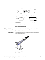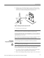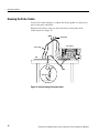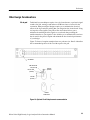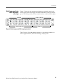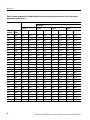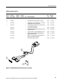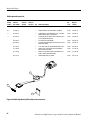
1
Instruction Manual
P69xx Series
High-Density Logic Analyzer Probes
with D-MaxtProbing Technology
071-1528-02
There are no current European directives that apply to this product. This product provides cable
and test lead connections to a test object of electronic measuring and test equipment.
Warning
The servicing instructions are for use by qualified
personnel only. To avoid personal injury, do not
perform any servicing unless you are qualified to
do so. Refer to all safety summaries prior to
performing service.
www.tektronix.com
Copyright © Tektronix, Inc. All rights reserved.
Tektronix products are covered by U.S. and foreign patents, issued and pending. Information in this publication supercedes
that in all previously published material. Specifications and price change privileges reserved.
Tektronix, Inc., P.O. Box 500, Beaverton, OR 97077
TEKTRONIX and TEK are registered trademarks of Tektronix, Inc.
Velcro is a registered trademark of Velcro Industries B.V.
cLGA is a registered trademark of InterCon Systems.
MagniVu, iView, PatGenVu, PowerFlex, QuickStart, TLAVu, KlipChip, and D-Max are trademarks of Tektronix, Inc.
Warranty 2
Tektronix warrants that this product will be free from defects in materials and workmanship for a period of one (1)
year from the date of shipment. If any such product proves defective during this warranty period, Tektronix, at its
option, either will repair the defective product without charge for parts and labor, or will provide a replacement in
exchange for the defective product. Parts, modules and replacement products used by Tektronix for warranty work
may be new or reconditioned to like new performance. All replaced parts, modules and products become the
property of Tektronix.
In order to obtain service under this warranty, Customer must notify Tektronix of the defect before the expiration
of the warranty period and make suitable arrangements for the performance of service. Customer shall be
responsible for packaging and shipping the defective product to the service center designated by Tektronix, with
shipping charges prepaid. Tektronix shall pay for the return of the product to Customer if the shipment is to a
location within the country in which the Tektronix service center is located. Customer shall be responsible for
paying all shipping charges, duties, taxes, and any other charges for products returned to any other locations.
This warranty shall not apply to any defect, failure or damage caused by improper use or improper or inadequate
maintenance and care. Tektronix shall not be obligated to furnish service under this warranty a) to repair damage
resulting from attempts by personnel other than Tektronix representatives to install, repair or service the product;
b) to repair damage resulting from improper use or connection to incompatible equipment; c) to repair any
damage or malfunction caused by the use of non-Tektronix supplies; or d) to service a product that has been
modified or integrated with other products when the effect of such modification or integration increases the time
or difficulty of servicing the product.
THIS WARRANTY IS GIVEN BY TEKTRONIX WITH RESPECT TO THE PRODUCT IN LIEU OF ANY
OTHER WARRANTIES, EXPRESS OR IMPLIED. TEKTRONIX AND ITS VENDORS DISCLAIM ANY
IMPLIED WARRANTIES OF MERCHANTABILITY OR FITNESS FOR A PARTICULAR PURPOSE.
TEKTRONIX’ RESPONSIBILITY TO REPAIR OR REPLACE DEFECTIVE PRODUCTS IS THE SOLE AND
EXCLUSIVE REMEDY PROVIDED TO THE CUSTOMER FOR BREACH OF THIS WARRANTY.
TEKTRONIX AND ITS VENDORS WILL NOT BE LIABLE FOR ANY INDIRECT, SPECIAL, INCIDENTAL,
OR CONSEQUENTIAL DAMAGES IRRESPECTIVE OF WHETHER TEKTRONIX OR THE VENDOR HAS
ADVANCE NOTICE OF THE POSSIBILITY OF SUCH DAMAGES.
Table of Contents
General Safety Summary . . . . . . . . . . . . . . . . . . . . . . . . . . . . . . . . . . . . . . . . . .
v
Preface . . . . . . . . . . . . . . . . . . . . . . . . . . . . . . . . . . . . . . . . . . . . . . . . . . .
vii
Related Documentation . . . . . . . . . . . . . . . . . . . . . . . . . . . . . . . . . . . . . . . . . . .
Commonly Used Terms . . . . . . . . . . . . . . . . . . . . . . . . . . . . . . . . . . . . . . . . . . .
Contacting Tektronix . . . . . . . . . . . . . . . . . . . . . . . . . . . . . . . . . . . . . . . . . . . . .
vii
viii
xi
Operating Basics . . . . . . . . . . . . . . . . . . . . . . . . . . . . . . . . . . . . . . . . . .
1
Product Description . . . . . . . . . . . . . . . . . . . . . . . . . . . . . . . . . . . . . . . . . . . . . .
P6960 High-Density Probe . . . . . . . . . . . . . . . . . . . . . . . . . . . . . . . . . . . . .
P6964 High-Density Probe . . . . . . . . . . . . . . . . . . . . . . . . . . . . . . . . . . . . .
P6980 High-Density Differential Probe . . . . . . . . . . . . . . . . . . . . . . . . . . .
P6982 High-Density Differential Probe . . . . . . . . . . . . . . . . . . . . . . . . . . .
Connecting the Probes to the Logic Analyzer . . . . . . . . . . . . . . . . . . . . . . . . . .
Connecting the Probes to the Target System . . . . . . . . . . . . . . . . . . . . . . . . . . .
Connecting the Flying Lead set . . . . . . . . . . . . . . . . . . . . . . . . . . . . . . . . .
Dressing the Probe Cables . . . . . . . . . . . . . . . . . . . . . . . . . . . . . . . . . . . . . . . . .
Storing the Probe Heads . . . . . . . . . . . . . . . . . . . . . . . . . . . . . . . . . . . . . . . . . . .
1
2
3
5
6
8
9
15
16
17
Reference . . . . . . . . . . . . . . . . . . . . . . . . . . . . . . . . . . . . . . . . . . . . . . . . .
19
Designing an Interface Between the Probes and a Target System . . . . . . . . . . .
Signal Fixturing Considerations . . . . . . . . . . . . . . . . . . . . . . . . . . . . . . . . .
Board Design . . . . . . . . . . . . . . . . . . . . . . . . . . . . . . . . . . . . . . . . . . . . . . . . . . .
Probe Dimensions . . . . . . . . . . . . . . . . . . . . . . . . . . . . . . . . . . . . . . . . . . . .
Retention Post Dimensions and Keepout . . . . . . . . . . . . . . . . . . . . . . . . . .
Side-by-side and End-to-end Layout Dimensions . . . . . . . . . . . . . . . . . . .
Signal Routing . . . . . . . . . . . . . . . . . . . . . . . . . . . . . . . . . . . . . . . . . . . . . . .
Mechanical Considerations . . . . . . . . . . . . . . . . . . . . . . . . . . . . . . . . . . . . .
Electrical Considerations . . . . . . . . . . . . . . . . . . . . . . . . . . . . . . . . . . . . . .
Probe Footprint Dimensions . . . . . . . . . . . . . . . . . . . . . . . . . . . . . . . . . . . . . . . .
Other Design Considerations . . . . . . . . . . . . . . . . . . . . . . . . . . . . . . . . . . . . . . .
Via-in-pad . . . . . . . . . . . . . . . . . . . . . . . . . . . . . . . . . . . . . . . . . . . . . . . . . .
Probe Pinout Definition and Channel Assignment . . . . . . . . . . . . . . . . . . . . . .
P6960 Single-ended Probe with D-Max probing technology . . . . . . . . . . .
P6964 Single-ended Probe with D-Max probing technology . . . . . . . . . . .
P6980 Differential Probe with D-Max probing technology . . . . . . . . . . . .
P6982 Differential Probe with D-Max probing technology . . . . . . . . . . . .
19
19
25
25
27
28
29
29
30
32
33
33
34
34
37
40
45
Specifications . . . . . . . . . . . . . . . . . . . . . . . . . . . . . . . . . . . . . . . . . . . . .
51
Mechanical and Electrical Specifications . . . . . . . . . . . . . . . . . . . . . . . . . . . . .
51
Maintenance . . . . . . . . . . . . . . . . . . . . . . . . . . . . . . . . . . . . . . . . . . . . . .
53
Probe Calibration . . . . . . . . . . . . . . . . . . . . . . . . . . . . . . . . . . . . . . . . . . . . . . . .
Functional Check . . . . . . . . . . . . . . . . . . . . . . . . . . . . . . . . . . . . . . . . . . . . . . . .
Inspection and Cleaning . . . . . . . . . . . . . . . . . . . . . . . . . . . . . . . . . . . . . . . . . . .
Service Strategy . . . . . . . . . . . . . . . . . . . . . . . . . . . . . . . . . . . . . . . . . . . . . . . . .
Legacy Probe and Attachment Support . . . . . . . . . . . . . . . . . . . . . . . . . . . . . . .
Repackaging Instructions . . . . . . . . . . . . . . . . . . . . . . . . . . . . . . . . . . . . . . . . . .
53
53
53
53
55
55
Replaceable Parts . . . . . . . . . . . . . . . . . . . . . . . . . . . . . . . . . . . . . . . . . .
Index . . . . . . . . . . . . . . . . . . . . . . . . . . . . . . . . . . . . . . . . . . . . . . . . . . . .
57
65
P69xx Series High-Density Logic Analyzer Probes Instruction Manual
i
Table of Contents
List of Tables
Table 1: Logic analyzer clock and qualifier availability . . . . . . . . . .
20
Table 2: 2X Demultiplexing source-to-destination
channel assignments . . . . . . . . . . . . . . . . . . . . . . . . . . . . . . . . . . . .
22
Table 3: 4X Demultiplexing source-to-destination
channel assignments . . . . . . . . . . . . . . . . . . . . . . . . . . . . . . . . . . . .
23
Table 4: Channel assignment for a P6960 single-ended data,
differential clock logic analyzer probe . . . . . . . . . . . . . . . . . . . . .
35
Table 5: Channel assignment for a P6964 single-ended data,
differential clock logic analyzer probe . . . . . . . . . . . . . . . . . . . . .
38
Table 6: Channel assignment for a P6980 differential clock and data logic
analyzer probe to a 136 or 102 channel logic analyzer module .
41
Table 7: Channel assignment for a P6980 differential clock and data logic
analyzer probe to a 68 or 34 channel logic analyzer module . . .
43
Table 8: Channel assignment for a P6982 differential clock and data logic
analyzer probe to a 136 or 102 channel logic analyzer module .
46
Table 9: Channel assignment for a P6982 differential clock and data logic
analyzer probe to a 68 or 34 channel logic analyzer module . . .
48
Table 10: Mechanical and electrical specifications . . . . . . . . . . . . . .
51
Table 11: Environmental specifications . . . . . . . . . . . . . . . . . . . . . . .
52
ii
P69xx Series High-Density Logic Analyzer Probes Instruction Manual
Table of Contents
List of Figures
Figure i: Differential input amplitude . . . . . . . . . . . . . . . . . . . . . . . . .
Figure ii: Flying Lead Set . . . . . . . . . . . . . . . . . . . . . . . . . . . . . . . . . . .
Figure iii: Probe example . . . . . . . . . . . . . . . . . . . . . . . . . . . . . . . . . . .
Figure 1: P6960 High-Density probe with
D-Max probing technology . . . . . . . . . . . . . . . . . . . . . . . . . . . . . . .
Figure 2: P6964 High-Density probe with
D-Max probing technology . . . . . . . . . . . . . . . . . . . . . . . . . . . . . . .
Figure 3: P6980 High-Density Differential probe with
D-Max probing technology . . . . . . . . . . . . . . . . . . . . . . . . . . . . . . .
Figure 4: P6982 High-Density Differential probe with
D-Max probing technology . . . . . . . . . . . . . . . . . . . . . . . . . . . . . . .
Figure 5: Connecting the probes to the logic analyzer . . . . . . . . . . . .
Figure 6: Replacing the wires on the retention posts . . . . . . . . . . . . .
Figure 7: Installing the retention posts in the PCB . . . . . . . . . . . . . .
Figure 8: Soldering the retention posts in the PCB . . . . . . . . . . . . . .
Figure 9: Proper handling of the interface clip . . . . . . . . . . . . . . . . . .
Figure 10: Connecting the probes to the target system . . . . . . . . . . .
Figure 11: Using the flying lead set to connect to the target system .
Figure 12: Proper dressing of the probe cables . . . . . . . . . . . . . . . . . .
Figure 13: Protecting the probe heads . . . . . . . . . . . . . . . . . . . . . . . . .
Figure 14: P6960, P6980, and P6982 probe dimensions . . . . . . . . . .
Figure 15: P6964 probe dimensions . . . . . . . . . . . . . . . . . . . . . . . . . . .
Figure 16: Retention post dimensions . . . . . . . . . . . . . . . . . . . . . . . . .
Figure 17: Keepout area . . . . . . . . . . . . . . . . . . . . . . . . . . . . . . . . . . . .
Figure 18: Side-by-side layout . . . . . . . . . . . . . . . . . . . . . . . . . . . . . . .
Figure 19: End-to-end layout . . . . . . . . . . . . . . . . . . . . . . . . . . . . . . . .
Figure 20: Signal routing on the target system . . . . . . . . . . . . . . . . . .
Figure 21: High-Density probe load model . . . . . . . . . . . . . . . . . . . . .
Figure 22: Probe footprint dimensions on the PCB . . . . . . . . . . . . . .
Figure 23: Optional Via-in-Pad placement recommendation . . . . . .
Figure 24: P6960 single-ended PCB footprint pinout detail . . . . . . .
Figure 25: P6964 single-ended PCB footprint pinout detail . . . . . . .
Figure 26: P6980 differential PCB footprint pinout detail . . . . . . . .
Figure 27: P6982 differential PCB footprint pinout detail . . . . . . . .
Figure 28: Replacing the cLGA clip . . . . . . . . . . . . . . . . . . . . . . . . . .
Figure 29: P6960 High-Density probe accessories . . . . . . . . . . . . . . .
P69xx Series High-Density Logic Analyzer Probes Instruction Manual
ix
ix
x
2
3
5
6
8
9
10
11
12
13
15
16
17
25
26
27
27
28
28
29
31
32
33
34
37
40
45
54
59
iii
Table of Contents
Figure 30: P6964 High-Density probe accessories . . . . . . . . . . . . . . .
Figure 31: P6980 High-Density Differential probe accessories . . . . .
Figure 32: P6982 High-Density Differential probe accessories . . . . .
Figure 33: Optional accessories . . . . . . . . . . . . . . . . . . . . . . . . . . . . . .
iv
60
61
62
63
P69xx Series High-Density Logic Analyzer Probes Instruction Manual
General Safety Summary
Review the following safety precautions to avoid injury and prevent damage to
this product or any products connected to it. To avoid potential hazards, use this
product only as specified.
Only qualified personnel should perform service procedures.
While using this product, you may need to access other parts of the system. Read
the General Safety Summary in other system manuals for warnings and cautions
related to operating the system.
To Avoid Fire or
Personal Injury
Connect and Disconnect Properly. Connect the probe output to the measurement
instrument before connecting the probe to the circuit under test. Disconnect the
probe input and the probe ground from the circuit under test before disconnecting
the probe from the measurement instrument.
Observe All Terminal Ratings. To avoid fire or shock hazard, observe all ratings
and markings on the product. Consult the product manual for further ratings
information before making connections to the product.
Do not apply a potential to any terminal, including the common terminal, that
exceeds the maximum rating of that terminal.
Avoid Exposed Circuitry. Do not touch exposed connections and components
when power is present.
Do Not Operate With Suspected Failures. If you suspect there is damage to this
product, have it inspected by qualified service personnel.
Do Not Operate in Wet/Damp Conditions.
Do Not Operate in an Explosive Atmosphere.
Keep Product Surfaces Clean and Dry.
Provide Proper Ventilation. Refer to the manual’s instructions for details on
installing the product so it has proper ventilation.
P69xx Series High-Density Logic Analyzer Probes Instruction Manual
v
General Safety Summary
Symbols and Terms
Terms in this Manual. These terms may appear in this manual:
WARNING. Warning statements identify conditions or practices that could result
in injury or loss of life.
CAUTION. Caution statements identify conditions or practices that could result in
damage to this product or other property.
Terms on the Product. These terms may appear on the product:
DANGER indicates an injury hazard immediately accessible as you read the
marking.
WARNING indicates an injury hazard not immediately accessible as you read the
marking.
CAUTION indicates a hazard to property including the product.
Symbols on the Product. The following symbol may appear on the product:
CAUTION
Refer to Manual
vi
P69xx Series High-Density Logic Analyzer Probes Instruction Manual
Preface
This document provides information on using and servicing the P69xx Series
logic analyzer probes.
Related Documentation
In addition to these probe instructions, the following documentation is available
for your Tektronix Logic Analyzers:
H
The Tektronix Logic Analyzer Family User Manual provides overall user
information for the TLA Series Logic Analyzer.
H
The TLA700 Series Logic Analyzer Installation Manual provides installation
information for the TLA700 Series Logic Analyzer.
H
The TLA5000 Series Logic Analyzer Installation Manual provides installation information for the TLA5000 Series Logic Analyzer.
H
The TLA7Axx/TLA7NAx Module Service Manual that provides module-level
service information for major components of the TLA Series Logic
Analyzer.
H
The P6434 Mass Termination Probe Instructions provides instructions for
using the P6434 Probes with older Tektronix logic analyzers.
H
The P6417 & P6418 Logic Analyzer Probes Instructions provides instructions for using the P6417 and P6418 Probes.
H
The P6419 Logic Analyzer Probe Instructions provides instructions for using
P6419 Probes.
H
P6810 General Purpose Logic Analyzer Probe Label Instructions
H
P6860 High Density Logic Analyzer Probe Label Instructions
H
P6864 High Density 4X Logic Analyzer Probe Label Instructions
H
P6880 High Density Differential Logic Analyzer Probe Label Instructions
H
P6960 High Density Logic Analyzer Probe Labeling and Installation
Instructions
H
P6964 High Density Logic Analyzer Probe Optimized for 4X Demultiplexing
Labeling and Installation Instructions
H
P6980 High Density Differential Logic Analyzer Probe Labeling and
Installation Instructions
P69xx Series High-Density Logic Analyzer Probes Instruction Manual
vii
Preface
H
P6982 High Density Differential Logic Analyzer Probe Optimized for 2X
Demultiplexing Labeling and Installation Instructions
H
The online help provides information about the user interface, the TLA700
Programmatic Interface (TPI), and the TLAScript interface. To view the
online help, select Help Topics from the Help menu. The TLAScript online
help provides links to related topics in TPI.
H
The online release notes provide last-minute product and software information not included in this manual. To access the Probe Manual Release Notes,
click Start > Programs > Tektronix Logic Analyzer > TLA Release Notes.
H
A series of microprocessor support instruction manuals provide operating
and service instructions for the individual microprocessor support packages.
Commonly Used Terms
Refer to the following list of commonly used terms throughout the manual.
cLGA
Compression Footprint
Differential Input
Amplitude Definition
viii
An acronym for compression Land Grid Array, a connector that provides an
electrical connection between a PCB and the probe input circuitry.
A connectorless, solderless contact between your PCB and the P69XX Series
probes. Connection is obtained by applying pressure between your PCB and the
probe through a cLGA c-spring.
For differential signals, the magnitude of the difference voltage Vmax-Vmin
(and Vmin-Vmax) must be greater than or equal to 150 mV. Refer to Figure i.
P69xx Series High-Density Logic Analyzer Probes Instruction Manual
Preface
Differential input (150 mV minimum swing each side, - 2.5 V maximum)
V
V max
1.15 V
V=V
0 V Difference
V
1V
V min
Differential equivalent signal input (300 mV swing) as viewed by the logic analyzer and the
analog probe output**.
150 mV
*V
0 V Difference
0V
TH = 0 V
- 150 mV
* Note: For differential inputs, the module threshold should be set to 0 V (assuming no
common mode error).
** Note: See online help for further analog output details.
Figure i: Differential input amplitude
D-Max probing technology
Flying Lead Set
Trademark name that describes the technology used in the P69xx Series
high-density logic analyzer probes.
A lead set designed to attach to a P6960 Probe to provide general-purpose
probing capability. See Figure ii.
CLK
SIG GND
Figure ii: Flying Lead Set
P69xx Series High-Density Logic Analyzer Probes Instruction Manual
ix
Preface
Functional Check
Procedure
Keepout Area
Module
Module End
PCB
Probe
Functional check procedures verify the basic functionality of the probes by
confirming that the probes recognize signal activity at the probe tips.
An area on a printed circuit board in which component, trace, and/or via
placement may be restricted.
The unit that plugs into a mainframe that provides instrument capabilities such
as logic analysis.
The end of the probe that plugs into the module unit.
An acronym for Printed Circuit Board; also known as Etched Circuit Board
(ECB).
The device that connects a module with a target system. See Figure iii.
Module end
Probe head
P6960 Single-ended
probe
Figure iii: Probe example
Probe Adapter
Probe Head
SMT KlipChip
x
A device that connects the LA module probe to a target system.
The end of the probe that connects to the target system or probe adapter.
An interface device for attaching logic analyzer probes to components with a
maximum lead diameter of 2.413 mm (0.095 in) and stackable on lead centers of
1.27 mm (0.050 in).
P69xx Series High-Density Logic Analyzer Probes Instruction Manual
Preface
Contacting Tektronix
Phone
1-800-833-9200*
Address
Tektronix, Inc.
Department or name (if known)
14200 SW Karl Braun Drive
P.O. Box 500
Beaverton, OR 97077
USA
Web site
www.tektronix.com
Sales support
1-800-833-9200, select option 1*
Service support
1-800-833-9200, select option 2*
Technical support
Email: [email protected]
1-800-833-9200, select option 3*
6:00 a.m. - 5:00 p.m. Pacific time
*
This phone number is toll free in North America. After office hours, please leave a
voice mail message.
Outside North America, contact a Tektronix sales office or distributor; see the
Tektronix web site for a list of offices.
P69xx Series High-Density Logic Analyzer Probes Instruction Manual
xi
Preface
xii
P69xx Series High-Density Logic Analyzer Probes Instruction Manual
Operating Basics
This section provides a brief description of the Tektronix P69xx Series HighDensity Logic Analyzer Probes, information on attaching color-coded probe
labels, and probe and adapter connection instructions from the logic analyzer to
the target system.
Product Description
The P69xx Series Probes connect TLA7Axx and TLA7NAx Series Logic
Analyzer modules to a target system.
Attaching Probe Labels
H
The P6960 probe consists of 34 single-ended channels in one probe head.
H
The P6964 probe consists of 34 single-ended channels in one probe head,
distributed over 4 module-end connectors.
H
The P6980 probe consists of 34 channels in two probe heads, with each head
containing 17 differential channels.
H
The P6982 probe consists of 17 differential channels in one probe head.
If you purchase probes for the logic analyzer module, you will need to apply the
color-coded labels. You will find instructions on how to attach the labels to the
probes on a color reference card that is included with the probes:
H
P6960 High Density Logic Analyzer Probe Labeling and Installation
Instructions
H
P6964 High Density Logic Analyzer Probe Optimized for 4X Demultiplexing
Labeling and Installation Instructions
H
P6980 High Density Differential Logic Analyzer Probe Labeling and
Installation Instructions
H
P6982 High Density Differential Logic Analyzer Optimized for 2X Demultiplexing Probe Labeling and Installation Instructions
P69xx Series High-Density Logic Analyzer Probes Instruction Manual
1
Operating Basics
P6960 High-Density Probe
The P6960 Probe is a 34-channel, high-density connectorless probe with D-Max
probing technology (see Figure 1). The probe consists of one probe head that has
34 channels (32 data and 2 clock/qual).
P6960 Single-ended
probe
Figure 1: P6960 High-Density probe with D-Max probing technology
The following list details the capabilities and qualities of the P6960 Probe:
2
H
Differential or single-ended clock and qualification inputs
H
Single-ended data inputs
H
cLGA contact eliminates need for built-in connector
H
Footprint supports direct signal pass-through
H
Supports PCB thickness of 1.27 mm to 6.35 mm (0.050 in to 0.250 in)
H
Consists of one independent probe head of 34 channels (32 data and
2 clock/quals)
H
Narrow 34-channel probe head makes for easier placement and layout
H
2X mode, (for example, 1:2 demultiplexing) uses one-half of the probe head
H
4X mode, (for example, 1:4 demultiplexing) uses one-quarter of the probe
head
H
Color-coded keyed attachment
H
--2.5 V to +5 V input operating range
H
--2.0 V to +4.5 V threshold range
P69xx Series High-Density Logic Analyzer Probes Instruction Manual
Operating Basics
H
300 mV minimum single-ended signal amplitude
H
150 mV amplitude each side minimum differential signal
H
Minimal loading of 0.5 pF at 20 kΩ to ground
H
Operation in normal or inverted polarity is acceptable (clock only)
H
Any common mode voltage is acceptable so long as the maximum positive
voltage does not exceed +5 V and the maximum negative voltage does not
exceed --2.5 V (clock only)
NOTE. Refer to Figure 20 on page 29 for P6960 probe routing and pinout
information.
P6964 High-Density Probe
The P6964 Probe is a 34-channel, high-density connectorless probe with D-Max
probing technology (see Figure 2). The probe consists of one probe head that has
34 channels (32 data and 2 clock/qual), distributed over 4 module-end connectors.
Figure 2: P6964 High-Density probe with D-Max probing technology
P69xx Series High-Density Logic Analyzer Probes Instruction Manual
3
Operating Basics
The following list details the capabilities and qualities of the P6964 Probe:
H
Differential or single-ended clock and qualification inputs
H
Single-ended data inputs
H
cLGA contact eliminates need for built-in connector
H
Footprint supports direct signal pass-through
H
Supports PCB thickness of 1.27 mm to 6.35 mm (0.050 in to 0.250 in)
H
Consists of one independent probe head of 34 channels (32 data and
2 clock/quals)
H
Narrow 34-channel probe head makes for easier placement and layout
H
Optimized for 4X mode (1:4 demultiplexing) to minimize board real estate
H
Color-coded keyed attachment
H
--2.5 V to +5 V input operating range
H
--2.0 V to +4.5 V threshold range
H
300 mV minimum single-ended signal amplitude
H
150 mV amplitude each side minimum differential signal
H
Minimal loading of 0.5 pF at 20 kΩ to ground
H
Operation in normal or inverted polarity is acceptable (clock only)
H
Any common mode voltage is acceptable so long as the maximum positive
voltage does not exceed +5 V and the maximum negative voltage does not
exceed --2.5 V (clock only)
NOTE. Refer to Figure 20 on page 29 for P6964 probe routing and pinout
information.
4
P69xx Series High-Density Logic Analyzer Probes Instruction Manual
Operating Basics
P6980 High-Density
Differential Probe
The P6980 Probe is a 34-channel, high-density connectorless differential probe
with D-Max probing technology (see Figure 3). The probe consists of two
independent probe heads of 17 channels each (16 data and 1 clock/qual).
Figure 3: P6980 High-Density Differential probe with D-Max probing technology
The following list details the capabilities and qualities of the P6980 Probe:
H
Differential data, clock and qualification inputs (single-ended signals may be
probed if negative input is grounded)
H
cLGA contact eliminates need for built-in connector
H
Footprint supports direct signal pass-through
H
Supports PCB thickness of 1.27 mm to 6.35 mm (0.050 in to 0.250 in)
H
Consists of two probe heads supporting 17 channels each, for a total of 34
channels
H
2X mode (1:2 demultiplexing) and 4X mode (1:4 demultiplexing), use one
probe head to minimize required board real estate
H
Color-coded keyed attachment
H
--2.5 V to +5 V input operating range
H
--2.0 V to +4.5 V threshold range
H
300 mV minimum single-ended signal amplitude (5 V maximum)
H
150 mV each side minimum differential signal amplitude (2.5 V maximum)
P69xx Series High-Density Logic Analyzer Probes Instruction Manual
5
Operating Basics
H
Minimal loading of 0.5 pF at 20 kΩ to ground
H
Operation in normal or inverted polarity is acceptable
H
Any common mode voltage is acceptable so long as the maximum positive
voltage does not exceed +5 V and the maximum negative voltage does not
exceed --2.5 V
NOTE. Refer to Figure 20 on page 29 for P6980 probe routing and pinout
information.
P6982 High-Density
Differential Probe
The P6982 Probe is a 17-channel, high-density connectorless differential probe
with D-Max probing technology (see Figure 4). The probe consists of one probe
head of 17 differential channels (16 data and 1 clock/qual).
Figure 4: P6982 High-Density Differential probe with D-Max probing technology
The following list details the capabilities and qualities of the P6982 Probe:
6
H
Differential data, clock and qualification inputs (single-ended signals may be
probed if negative input is grounded)
H
cLGA contact eliminates need for built-in connector
H
Footprint supports direct signal pass-through
H
Supports PCB thickness of 1.27 mm to 6.35 mm (0.050 in to 0.250 in)
P69xx Series High-Density Logic Analyzer Probes Instruction Manual
Operating Basics
H
Consists of one probe head supporting 17 channels
H
Optimized for 2X mode (1:2 demultiplexing) to minimize required board
real estate
H
Color-coded keyed attachment
H
--2.5 V to +5 V input operating range
H
--2.0 V to +4.5 V threshold range
H
300 mV minimum single-ended signal amplitude (5 V maximum)
H
150 mV each side minimum differential signal amplitude (2.5 V maximum)
H
Minimal loading of 0.5 pF at 20 kΩ to ground
H
Operation in normal or inverted polarity is acceptable
H
Any common mode voltage is acceptable so long as the maximum positive
voltage does not exceed +5 V and the maximum negative voltage does not
exceed --2.5 V
NOTE. Refer to Figure 20 on page 29 for P6982 probe routing and pinout
information.
P69xx Series High-Density Logic Analyzer Probes Instruction Manual
7
Operating Basics
Connecting the Probes to the Logic Analyzer
Refer to Figure 5 and connect the probes to the logic analyzer according to the
following steps.
1. Identify the beveled edges of the connector inside the module end of the
probe.
2. Align the beveled edges of the connector to its mating connector on the logic
analyzer module and press into place.
3. Use care to evenly tighten both screws on the module end of the probe until
they are snug. First slightly tighten both screws, then snug each screw to
4 in-lbs (max).
NOTE. All P69xx series Logic Analyzer probes can be connected to the logic
analyzer when it is powered on. In addition, all P69xx series Logic Analyzer
probes connect to the logic analyzer in exactly the same manner.
Probe
Match
color-- coded
labels
Figure 5: Connecting the probes to the logic analyzer
8
P69xx Series High-Density Logic Analyzer Probes Instruction Manual
Operating Basics
Connecting the Probes to the Target System
You can connect the P69xx Series Probes to the target system without turning off
the power to the target system. The target system must have the probe retention
posts installed; if your system does not have the posts, see the procedure below.
Using the Correct Retention Post Wires. If the PCB is ≤ .120 in thick, use the wire
that comes preattached to the posts. If the PCB is > .120 in thick, use the longer
wire that is included with the posts.
The longer wires are embedded in the protective foam of the retention post kit.
Make sure that you use the longer wires included in the kit when the PCB is
> .120 in thick. To install the longer wires on the retention posts, refer to
Figure 6 and do the following:
1. Remove the old wire by pulling the side of the wire over the retaining tab
and lifting the wire away from the post.
2. Place the new wire in the slot side without the tab, and then wrap the wire
over the tab side until it engages in the slot (you will feel or hear a slight
click).
Tab
Tab
Figure 6: Replacing the wires on the retention posts
P69xx Series High-Density Logic Analyzer Probes Instruction Manual
9
Operating Basics
Installing the Retention Posts. To install the retention posts on the PCB, do the
following:
1. On the retention post/carrier assembly, locate the black retention post (the
post with the keying pin) and align it to the keying pin hole on the PCB.
(See Figure 7.)
2. Press the retention posts into the holes on the footprint on the PCB.
NOTE. The following two steps — bending and soldering the wires to the circuit
board — are the two most important steps in assuring that the probe retaining
posts are correctly mounted. Bending the wires before soldering them helps
prevent long-term cold solder flow.
3. Press down on the carrier and bend the post wires out to anchor the posts to
the PCB. Ensure the assembly is perpendicular to the PCB when bending
and soldering the post wires.
The bend point in the retaining wire should be as close to the circuit board
surface as possible. Grip the wire with a pair of needle--nose pliers about
1/8--inch above the circuit board surface and let the side of the through-hole
(not the pliers) act as the fulcrum point for bending the wire. This method
pulls the probe mounting posts tightly against the circuit board surface.
Press down on
the carrier
Keying pin
hole
90
~0
≤ 45°
Figure 7: Installing the retention posts in the PCB
10
P69xx Series High-Density Logic Analyzer Probes Instruction Manual
Operating Basics
4. Solder the posts to the PCB. (See Figure 8 on page 11.) The posts can be
soldered from the top or bottom of the circuit board, but it is best to solder
the bottom to avoid the heat-sinking effects of the posts on top.
Remove
the carrier
Solder the
wires
Figure 8: Soldering the retention posts in the PCB
5. Pull off the carrier from the posts.
NOTE. The posts may have a small amount of movement after you solder them to
the circuit board. This is normal and accounted for in the post design.
The probe should mate firmly to the board when the two screws are tightened to
the mounting posts. The screws have a mechanical stop on them to prevent overtightening the probe to the board.
After a probe has been installed and removed, there may be slightly more play in
the posts. This is also normal and accounted for in the probe design.
Cleaning the
Compression Footprints
The following procedure is recommended to obtain best performance.
CAUTION. To avoid electrical damage, always power off your target system
before cleaning the compression footprint.
Prior to connecting the probe to the target system, the compression footprints on
the board should be properly cleaned, according to the following steps:
1. Use a lint-free, clean-room cloth lightly moistened with electronic/reagent
grade isopropyl alcohol, and gently wipe the footprint surface.
2. Remove any remaining lint using a nitrogen air gun or clean, oil-free dry air.
P69xx Series High-Density Logic Analyzer Probes Instruction Manual
11
Operating Basics
Handling the cLGA
Interface Clips
(Probe Heads)
The cLGA interface clips in the probe heads should always be handled with care.
Keep the following points in mind when you handle the clips:
H
The cLGA interface clips should always be handled by the outer edges,
being careful to avoid the contacts in the center. Contacts should not be
touched with fingers, tools, wipes, or any other devices. See Figure 9.
Figure 9: Proper handling of the interface clip
12
H
The connector should not be exposed to liquids or dry chemicals.
H
If the board pad array needs to be cleaned, only use isopropyl alcohol and
lint-free cloth as described above.
H
Immediately following cleaning, or immediately prior to placement of
connector to circuit board, the board pad array and connector contact array
should be blown off with clean, oil-free dry air or nitrogen to remove loose
debris. First start the blowing process by aiming away from the array areas,
and then sweep across the pad and contact arrays in a repeated motion to
remove loose debris.
H
The connector should be placed onto the board pad array using the bosses or
locator pins for alignment. Care should be taken to prevent incidental contact
with other surfaces or edges in the connector contact array area prior to board
placement.
H
Always store the probe head in the protective cover when not in use.
See Figure 13 on page 17.
P69xx Series High-Density Logic Analyzer Probes Instruction Manual
Operating Basics
Connect the Probe
Refer to Figure 10, and connect the probes using the following steps.
1. Align the black screw on the probe with the black post on the PCB.
Black
p
P6960
Single-- ended
Black
Retention posts
Note: Both the screws and retention
posts are visually keyed (one set is black
and one set is silver).
Figure 10: Connecting the probes to the target system
2. Start both screws in the posts, and tighten them evenly to ensure that the
probe approaches and mates squarely to the PCB. If access is limited, use the
adjustment tool that came with your probe. The probe is completely fastened
to the PCB when the screws stop in the posts.
3. Verify that all of the channels are functional. If any channels appear to be
nonfunctional, see Troubleshooting Probe Connections to the DUT on
page 14.
P69xx Series High-Density Logic Analyzer Probes Instruction Manual
13
Operating Basics
Troubleshooting Probe
Connections to the DUT
The most obvious symptom of a problem with the mounting post installation is
seeing incorrect data in the logic analyzer acquisition. However, the nature of the
incorrect data has a very consistent characteristic; the data from multiple
channels go to a logic low and stay there. Intermittent bad data, or a single dead
channel are not failures typically associated with probe mounting post installation problems.
1. Slightly move the probe head to either side, or press down on the probe head
while making new acquisitions. If good data is now being acquired, then the
probe mounting is most likely the cause.
2. If good data is not acquired, then remove the probe and check the posts for
too much play. If there is significant play, then the probe mounting is most
likely the cause.
3. If the posts have minimal play and you cannot see a gap between the bottom
of the posts and the circuit board surface, then move the probe with bad data
from one logic analyzer probe location to another.
4. If the problem follows the probe, then the probe is the problem. Visually
inspect the cLGA interface clip on the probe for any damage or missing
c-spring metal contacts.
If there is damage to the interface clip, or if any c-spring metal contacts are
missing, replace the cLGA interface clip. (See Replacing the cLGA Clip on
page 54 and Replaceable Parts, beginning on page 57 for more information.)
5. If the problem doesn’t follow the probe, it is either the logic analyzer or the
probe connection at its previous location. Move the probe back to the
original location to be certain it was not a connection problem at the logic
analyzer end.
6. Place another probe in the mounting posts of the original probe. If the new
probe acquires data, then the old probe is probably at fault.
14
P69xx Series High-Density Logic Analyzer Probes Instruction Manual
Operating Basics
Connecting the Flying
Lead set
The flying lead set, Tektronix part number 196-3494-xx, is an optional
accessory for your probe. The flying lead set allows you to connect to individual
test points on your PCB. However, for general-purpose probing, the P6810 probe
is recommended for best performance.
Refer to Figure 11 and connect the probe to the target system by performing the
steps that follow. You can connect the probe leads to the target system without
turning off the power to the target system.
1. Connect the probe leads to the square pins on the PCB.
2. Connect the negative input to ground on the PCB.
3. Connect the leadset to the probe.
CLK
SIG GND
Figure 11: Using the flying lead set to connect to the target system
P69xx Series High-Density Logic Analyzer Probes Instruction Manual
15
Operating Basics
Dressing the Probe Cables
Use the Velcro cable managers to combine the cables together or to help relieve
strain on the probe connections.
Hang the probe cables so that you relieve the tension on the probes at the
retention posts. See Figure 12.
Good
Cable hanger
Logic Analyzer
Probe cables
PCB
Bad
Bad contact
Figure 12: Proper dressing of the probe cables
16
P69xx Series High-Density Logic Analyzer Probes Instruction Manual
Operating Basics
Storing the Probe Heads
To protect the interface clip, it is important to properly store the probe heads
when the probes are not in use. See Figure 13.
Gently slide the probe cover over the probe end and store the probe.
Protective
cover
Figure 13: Protecting the probe heads
P69xx Series High-Density Logic Analyzer Probes Instruction Manual
17
Operating Basics
18
P69xx Series High-Density Logic Analyzer Probes Instruction Manual
Reference
This section provides reference information for the P69xx Series High-Density
Probes with D-Max probing technology. Topics include the following:
H
Designing an interface between the probe and a target system
H
Board design
H
Probe footprint dimensions
H
Probe pinout and channel assignment
Designing an Interface Between the Probes and a Target System
Once you have determined which probe is required, use the following information to design the appropriate connector into your target system board.
The following topics are in this section:
Signal Fixturing
Considerations
H
Signal fixturing considerations
H
Signal connections (signal names and footprints)
H
Mechanical considerations
H
Electrical considerations
This section contains the following information to consider for signal fixturing:
H
Clocks and qualifiers
H
Merged modules and source synchronous clocking
H
Demultiplexing multiplexed buses
H
2X and 4X high resolution timing modes (Internal 2X and 4X)
H
Probing analog signals
H
Range recognition
P69xx Series High-Density Logic Analyzer Probes Instruction Manual
19
Reference
Clocks and Qualifiers. Every logic analyzer has some special purpose input
channels. Inputs designated as clocks can cause the analyzer to store data.
Qualifier channels can be logically ANDed and ORed with clocks to further
define when the analyzer should latch data from the system under test. Routing
the appropriate signals from your design to these inputs ensures that the logic
analyzer can acquire data correctly. Unused clocks can be used as qualifier
signals.
Depending on the channel width, each TLA7Axx and TLA7NAx Series logic
analyzer module will have a different set of clock and qualifier channels. Table 1
shows the clock and qualifier channels available for each module.
Table 1: Logic analyzer clock and qualifier availability
TLA7Axx/
TLA7NA
TLA7NAx
Module
CLK:0
TLA7AA1
n
TLA7AA2
n
n
n
n
TLA7AA3
n
n
n
TLA7AA4
n
n
TLA7AB2
n
TLA7AB4
n
TLA7NA1
n
TLA7NA2
n
n
n
n
TLA7NA3
n
n
n
TLA7NA4
n
n
n
Clock Inputs
CLK:1
CLK:2
Qualifier Inputs
CLK:3
QUAL:0
QUAL:1
QUAL:2
QUAL:3
n
n
n
n
n
n
n
n
n
n
n
n
n
n
n
n
n
n
n
n
n
n
n
n
n
n
n
n
n
All clock and qualifier channels are stored. The analyzer always stores the logic
state of these channels every time it latches data.
Since clock and qualifier channels are stored in the analyzer memory, there is no
need to double probe these signals for timing analysis. When switching from
state to timing analysis modes, all of the clock and qualifier signals will be
visible. This allows you to route signals not needed for clocking to the unused
clock and qualifier channels.
It is a good practice to take advantage of the unused clock and qualifier channels
to increase your options for when you will latch data. Routing several clocks and
strobes in your design to the analyzer clock inputs will provide you with a
greater flexibility in the logic analyzer clocking setup menus.
20
P69xx Series High-Density Logic Analyzer Probes Instruction Manual
Reference
As an example, look at a microprocessor with a master clock, data strobe, and an
address strobe. Routing all three of these signals to analyzer clock inputs will
enable you to latch data on the processor master clock, only when data is
strobed, or only when address is strobed. Some forethought in signal routing can
greatly expand the ways in which you can latch and analyze data.
A microprocessor also provides a good example of signals that can be useful as
qualifiers. There are often signals that indicate data reads versus data writes
(R/W), signals that show when alternate bus masters have control of the
processor buses (DMA), and signals that show when various memory devices are
being used (ChipSel). All of these signals are good candidates for assignment to
qualifier channels.
By logically ANDing the clock with one of these qualifiers you can program the
analyzer to store only data reads or data writes. Using the DMA signal as a
qualifier provides a means of filtering out alternate bus master cycles. Chip
selects can limit data latching to specific memory banks, I/O ports, or peripheral
devices.
Merged Module Sets and Source Synchronous Clocking. TLA7Axx and
TLA7NAx analyzer modules that are 102 channels or 136 channels wide can be
merged together to act as a single logic analyzer with a larger channel count. Up
to five modules can be merged to provide up to a 680 channel analyzer. A unique
feature of the TLA7Axx module is that it supports source synchronous clocking.
Combining these two capabilities provide some additional considerations for
signal routing.
Source synchronous clocking is a method that manages the skew between the
system clock and the data bus by requiring the sending device to drive an actual
clock or strobe signal along with the data that is very tightly coupled with it in
terms of skew. The receiving device then uses this strobe to capture the data.
A variant of this scheme is being applied to large microprocessor buses, where
the bus is split into smaller, more easily managed groups that each have their
own dedicated strobe. Although the timing relationship between a particular
clock and its associated data group is very tight, the timing between the different
groups can vary greatly and changes depending on which device has control of
the bus.
Many source synchronous designs use wide buses. It is not uncommon to require
a set of merged logic analyzer modules to provide the channel count needed in
probing larger source synchronous systems. While all of the modules in a
merged set can use their clock inputs independently if needed, it must be
remembered that there are a maximum of four clock inputs on a 136 channel
wide module.
P69xx Series High-Density Logic Analyzer Probes Instruction Manual
21
Reference
To see the importance of this reminder we will once again use a microprocessor
system as an example. Tektronix logic analyzer processor has a 32 bit address
bus and a 64 bit data bus. The data bus is split into four 16 bit subgroups that
have independent source synchronous clocks. For the logic analyzer to correctly
acquire data from this system it will need five clock inputs, one for the address
bus and one each for the four 16 bit data bus subgroups.
To acquire both buses, the analyzer would need at least 96 channels (32 address
and 64 data). However, a single 102 channel card doesn’t have the required five
clock inputs. By merging two 102 channel modules into a set you can obtain the
needed number of clock inputs. Route the address bus to one module in the set
and route the data bus, along with its four source synchronous clocks, to the
second module in the set.
Demultiplexing Multiplexed Buses. TLA7Axx modules support both 2X and 4X
demultiplexing. TLA7NAx modules support 2X demultiplexing. Each signal on
a dual or quad multiplexed bus can be demultiplexed into its own logic analyzer
channel. See Tables 2 and 3 to determine the correct channel groups to use.
Table 2: 2X Demultiplexing source-to-destination channel assignments
Source
connecting
channel groups
Destination channels receiving target system test data
TLA7AA4/
TLA7NA4
TLA7AA3/
TLA7NA3
TLA7AA2/
TLA7NA2
TLA7AA1/
TLA7NA1
TLA7AB4
TLA7AB2
A3:7-- 0
D3:7-- 0
D3:7-- 0
C3:7-- 0
C3:7-- 0
D3:7-- 0
C3:7-- 0
A2:7-- 0
D2:7-- 0
D2:7-- 0
C2:7-- 0
C2:7-- 0
D2:7-- 0
C2:7-- 0
A1:7-- 0
D1:7-- 0
D1:7-- 0
D1:7-- 0
D1:7-- 0
D1:7-- 0
A0:7-- 0
D0:7-- 0
D0:7-- 0
D0:7-- 0
D0:7-- 0
D0:7-- 0
C3:7-- 0
C1:7-- 0
C1:7-- 0
C1:7-- 0
C2:7-- 0
C0:7-- 0
C0:7-- 0
C0:7-- 0
E3:7-- 0
E1:7-- 0
E1:7-- 0
E2:7-- 0
E0:7-- 0
E0:7-- 0
CLK:0
QUAL:1
QUAL:1
QUAL:1
CLK:1
QUAL:0
QUAL:0
QUAL:0
CLK:2
QUAL:3
QUAL:3
CLK:3
QUAL:2
QUAL:2
22
P69xx Series High-Density Logic Analyzer Probes Instruction Manual
Reference
Table 3: 4X Demultiplexing source-to-destination channel assignments
Source
connecting
ti
channel groups
Destination channels receiving target system test data
TLA7AA4
TLA7AA3
TLA7AA2
TLA7AA1
TLA7AB4
TLA7AB2
C3:7-- 0
C2:7-- 0
C1:7-- 0
C0:7-- 0
C2:7-- 0
C1:7-- 0
C0:7-- 0
A3:7-- 0
A2:7-- 0
C2:7-- 0
A3:7-- 0
A2:7-- 0
C2:7-- 0
C2:7-- 0
C1:7-- 0
C0:7-- 0
A3:7-- 0
A2:7-- 0
C2:7-- 0
A1:7-- 0
A0:7-- 0
D1:7-- 0
D0:7-- 0
A0:7-- 0
D1:7-- 0
D0:7-- 0
A0:7-- 0
D1:7-- 0
D0:7-- 0
A0:7-- 0
D1:7-- 0
D0:7-- 0
A0:7-- 0
D1:7-- 0
D0:7-- 0
A3:7-- 0
A2:7-- 0
D3:7-- 0
D2:7-- 0
A2:7-- 0
D3:7-- 0
D2:7-- 0
E3:7-- 0
E2:7-- 0
E1:7-- 0
E0:7-- 0
E2:7-- 0
E1:7-- 0
E0:7-- 0
CLK:3
CLK:2
QUAL:3
QUAL:2
CLK:2
QUAL:3
QUAL:2
CLK:1
CLK:0
QUAL:1
QUAL:0
CLK:0
QUAL:1
QUAL:0
A2:7-- 0
D3:7-- 0
D2:7-- 0
CLK:0
QUAL:1
QUAL:0
When demultiplexing data there is no need to connect the destination channels to
the multiplexed bus. Data from the source channels are routed to the destination
channels internal to the logic analyzer. Tables 2 and 3 show the mapping of
source channels to destination channels.
Demultiplexing affects only the main memory for the destination channels. This
means that the MagniVu memory is filled with data from whatever is connected
to the demultiplexing destination channel probe inputs. This provides an
opportunity to acquire high resolution MagniVu data on a few extra channels.
Connecting the demultiplexing destination channels to other signals will allow
viewing of their activity in the MagniVu memory but not the main memory.
2X and 4X High Resolution Timing Modes. The 2X high resolution timing mode
provides double the normal 500 MHz sample rate on one-half of the channels.
By trading half of the analyzer’s channels, the remaining channels can be
sampled at a 1 GHz rate with double the memory depth. Likewise, 4X high
resolution timing mode provides quadruple the normal 500 MHz sample rate on
one-fourth of the channels. By trading three-fourths of the analyzer’s channels,
the remaining channels can be sampled at a 2 GHz rate with quadruple the
memory depth.
P69xx Series High-Density Logic Analyzer Probes Instruction Manual
23
Reference
Both of the high resolution timing modes use the same demultiplexing channel
routing as shown in Tables 2 and 3. By taking care to assign critical signals to
the demultiplexing source channels, you can obtain extra timing resolution where
it is most needed. Since demultiplexing affects only the main memory you will
still have the MagniVu data available for all of the signals that are disconnected
from the main memory when you switch to the high resolution timing modes.
Probing Analog Signals. The TLA7Axx module provides visibility of analog
signals with Analog mux. Analog mux routes the actual signal seen by each
channel’s probe through a high bandwidth path to an analog multiplexer inside of
the logic analyzer module. From the logic analyzer interface, you can route any
input channel to one of four output connectors on the module. By connecting the
analyzer analog outputs to your oscilloscope, you can see the analog characteristics of any signal probed by the logic analyzer.
Sometimes it is convenient to have analog signals accessible for easier probing.
Signals such as A/D Converter inputs, D/A Converter outputs, low voltage
power supplies, termination voltages, and oscillator outputs are just a few
examples. Routing these signals to unused logic analyzer inputs provides a quick
method of viewing their activity without ever picking up an oscilloscope probe.
Care must be taken to ensure that such signals are voltage limited and will not
exceed the maximum nondestructive input voltage for the logic analyzer probes
of ±15 Vpeak.
Range Recognition. When using range recognizers, the probe groups and probe
channels must be in hardware order. Probe groups must be used from the
most-significant probe group to the least-significant probe group based on the
following order:
C3 C2 C1 C0 E3 E2 E1 E0 A3 A2 D3 D2 A1 A0 D1 D0 Q3 Q2 Q1 Q0 CK3
CK2 CK1 CK0
Probe channels must be from the most-significant channel to the least-significant
channel based on the following order:
76543210
The above examples assumes a 136-channel LA module. The missing channels
in LA modules with fewer than 136 channels are ignored. With merged modules,
range recognition extends across the first three modules: the master module
contains the most-significant channels.
24
P69xx Series High-Density Logic Analyzer Probes Instruction Manual
Reference
Board Design
This section provides information that helps you design your PCB mechanically
and electrically for use with the P69xx Series Probes.
Probe Dimensions
Figure 14 shows the probe dimensions for the P6960, P6980, and P6982 probes.
Figure 15 on page 26 shows the probe dimensions for the P6964 probe.
32.56 mm
(1.282 in)
182.88 mm
(72.00 in)
60.19 mm
(2.37 in)
P6960
32.56 mm
(1.282 in)
182.88 mm
(72.00 in)
60.19 mm
(2.37 in)
182.88 mm
(72.00 in)
60.19 mm
(2.37 in)
P6980
32.56 mm
(1.282 in)
P6982
4.60 mm
(0.181 in)
Figure 14: P6960, P6980, and P6982 probe dimensions
P69xx Series High-Density Logic Analyzer Probes Instruction Manual
25
Reference
32.56 mm
(1.282 in)
182.88 mm
(72.00 in)
60.19 mm
(2.37 in)
P6964
4.60 mm
(0.181 in)
Figure 15: P6964 probe dimensions
26
P69xx Series High-Density Logic Analyzer Probes Instruction Manual
Reference
Retention Post
Dimensions and Keepout
The probes are attached to the PC board using two retention posts which ensures
a reliable electrical and mechanical connection to your design, pin-to-pad
alignment, and holds the probe securely to the board. Board thicknesses that are
supported include 1.27 mm (0.050 in) to 6.35 mm (0.250 in). Figure 16 shows
the dimensions of the retention posts.
CAUTION. To avoid solder creep, bend the post wires out after you insert the
posts in the board, and then solder the post wires. You can solder the retention
wires from the top or bottom of the circuit board.
4.57 mm
(0.180 in)
33.83 mm
(1.322 in)
10.92 mm
(0.430 in)
Retention
post wires
Figure 16: Retention post dimensions
Figure 17 shows the keep out area required for the retention posts. Vias must be
placed outside of the keepout area. Any traces routed on the top layer of the
board must stay outside of the keepout area. Traces may be routed on inner
layers of the board through the keepout area.
3.40 mm
(0.134 in)
3.51 mm
(0.138 in)
Keepout area
Figure 17: Keepout area
P69xx Series High-Density Logic Analyzer Probes Instruction Manual
27
Reference
Side-by-side and
End-to-end Layout
Dimensions
Figure 18 shows the dimensions for side-by-side footprint layout.
34.04 mm
(1.340 in)
9.40 mm
(0.370 in)
Figure 18: Side-by-side layout
Figure 19 shows the dimensions for an end-to-end footprint layout.
34.04 mm
(1.340 in)
34.04 mm
(1.340 in)
4.70 mm
(0.185 in)
Figure 19: End-to-end layout
28
P69xx Series High-Density Logic Analyzer Probes Instruction Manual
Reference
Signal Routing
Figure 20 shows examples of pass-through signal routing for a single-ended data
configuration and a differential data configuration.
Ground
Signal pads
Ground
Signal pads
Single-- ended pinout
Differential pinout
Figure 20: Signal routing on the target system
Mechanical
Considerations
This section provides information on compression footprint requirements and
physical attachment requirements.
The PCB holes, in general, do not have an impact upon the integrity of your
signals when the signals routed around the holes have the corresponding return
current plane immediately below the signal trace for the entire signal path from
driver to receiver.
NOTE. For optimum signal integrity, there should be a continuous, uninterrupted
ground return plane along the entire signal path.
P69xx Series High-Density Logic Analyzer Probes Instruction Manual
29
Reference
Physical Attachment Requirements for the P69xx Series Probes.
The P69xx Series Probe interconnects are designed to accommodate PCB
thickness ranging from 1.27 mm to 6.35 mm (0.050 in to 0.250 in). To accommodate this range, there are two wire lengths in the design:
H
For board thicknesses of 0.050 in to 0.120 in, use the standard wire that
comes mounted to the post in the retention kit included with each probe.
H
For board thicknesses of 0.120 in to 0.250 in, use the long wire supplied
with the probe (also included in the retention kit, embedded in foam).
For more information, see Using the Correct Retention Post Wires on page 9.
Electrical Considerations
This section provides information on transmission lines and load models for the
P69xx Series Probes.
The low-frequency model is typically adequate for rise and fall times of 1 ns or
slower in a typical 25 Ω source impedance environment (50 Ω runs with a
pass-through connection). For source impedance outside this range, and/or rise
and fall times faster than 1 ns, use the high-frequency model to determine if a
significant difference is obtained in the modeling result.
The compression land pattern pad is not part of the load model. Make sure that
you include the compression land pad in the modeling.
Transmission Lines. Due to the high performance nature of the interconnect,
ensure that stubs, which are greater than 1/4 length of the signal rise time, are
modeled as transmission lines.
30
P69xx Series High-Density Logic Analyzer Probes Instruction Manual
Reference
P69xx Series Probes Load Model. The following electrical model (see Figure 21)
includes a low-frequency and high-frequency model of the High-Density
Single-Ended and High-Density Differential Probes. For the Differential Probes,
the load model is applied to both the + side and the -- side of the signal.
R1
20k Ω
C1
0.5 pF
Low frequency probe load
td =10 pS
Z0=85 Ω
td =6 pS
Z0=70 Ω
+
+
+
Pad_C
40 fF
160 fF
20k Ω
High frequency probe load
Figure 21: High-Density probe load model
The differential load for the P6960 and P6964 clock inputs and the P6980 and
P6982 probes can be modeled by attaching the single line model to each side
(+ and --) of the differential signal. The + and -- sides of the differential signal are
well insulated in the probe head up to and including the differential input stage.
P69xx Series High-Density Logic Analyzer Probes Instruction Manual
31
Reference
Probe Footprint Dimensions
Use the probe footprint dimensions in Figure 22 to lay out your circuit board
pads and holes for attaching the retention posts. Pad finishes that are supported
include immersion gold, immersion silver, and hot air solder level.
NOTE. Tektronix recommends using immersion gold surface finish for best
performance.
Tektronix also recommends that the probe attachment holes float or remain
unconnected to a ground plane. This prevents overheating the ground plane and
promotes quicker soldering of the retention posts to your PCB. The probe
retention posts are designed to allow you to solder the retention posts from either
side of your PCB.
34.04 mm
(1.340 in)
0.84 mm
(0.033 in)
Nonplated thru hole
31.95 mm
(1.258 in)
26 mm
(1.024 in)
1.72 mm
(0.068 in)
2.35 mm
(0.0925 in)
1 mm typical
(0.03937 in)
4x dia. 0.71 mm
(0.028 in)
Plated thru hole
4.7 mm
(0.185 in)
1.72 mm
(0.068 in)
1.04 mm
(0.041 in)
0.64 mm
(0.025 in)
0.71 mm
(0.028 in)
0.58 mm
(0.023 in)
4X dia. 1.22 mm
(0.048 in)
Annular ring
1.27 mm
(0.050 in)
2.98 mm
(0.117 in)
Figure 22: Probe footprint dimensions on the PCB
NOTE. You must maintain a solder mask web between the pads when traces are
routed between pads on the same layer. The solder mask must not encroach onto
the pads within the pad dimensions shown in Figure 17 on page 27.
32
P69xx Series High-Density Logic Analyzer Probes Instruction Manual
Reference
Other Design Considerations
Via-in-pad
Traditional layout techniques require vias to be located next to a pad and a signal
routed to the pad, causing a stub and more PCB board area to be used for the
connection. Many new digital designs require you to minimize the electrical
effects of the logic analyzer probing that you design into the circuit board. Using
via-in-pad to route signals to the pads on the circuit board allows you to
minimize the stub length of the signals on your board, thus providing the
smallest intrusion to your signals. It also enables you to minimize the board area
that is used for the probe footprint and maintain the best electrical performance
of your design.
Figure 23 shows a footprint example where two pads use vias. Detail A describes
the recommended position of the via with respect to the pad.
See detail A
Max via dia 0.25
mm (0.010 in)
Dia 0.51 mm
(0.020 in)
0.04 mm
(0.002 in)
0.32 mm
(0.013 in)
Detail A
Scale 50.000
Figure 23: Optional Via-in-Pad placement recommendation
P69xx Series High-Density Logic Analyzer Probes Instruction Manual
33
Reference
Probe Pinout Definition and Channel Assignment
This section contains probe pinout definitions and channel assignment tables for
the P69xx Series Probes.
P6960 Single-ended Probe
with D-Max probing
technology
G
Figure 24 shows the pad assignments, pad numbers, and signal names for the
PCB footprint of the P6960 single-ended data, differential clock logic analyzer
probe. The P6960 probe has 32 data channels, one clock, and one qualifier for
each footprint.
D2 D3 G D6 D7 G D8 D9 G D12 D13 G D16 D17 G D20 D21 G CK2-- CK2+ G D26 D27 G D30 D31
B27
B1
A27
A1
D0 D1 G D4 D5 G CK1+ CK1-- G D10 D11 G D14 D15 G D18 D19 G D22 D23 G D24 D25 G D28 D29 G
Figure 24: P6960 single-ended PCB footprint pinout detail
Table 4 on page 35 lists the channel mapping to a logic analyzer module for a
P6960 single-ended data, differential clock logic analyzer probe.
34
P69xx Series High-Density Logic Analyzer Probes Instruction Manual
Reference
Table 4: Channel assignment for a P6960 single-ended data, differential clock logic analyzer probe
136 Channel
68 Channel
102 Channel
34 Channel
Pin Number
Signal name
Probe4
Probe 3
Probe 2
Probe 1
Probe 2
Probe 1
A1
D0
E2:0
A2:0
A0:0
C2:0
A0:0
C2:0
A2
D1
E2:1
A2:1
A0:1
C2:1
A0:1
C2:1
A3
GND
GND
GND
GND
GND
GND
GND
A4
D4
E2:4
A2:4
A0:4
C2:4
A0:4
C2:4
A5
D5
E2:5
A2:5
A0:5
C2:5
A0:5
C2:5
A6
GND
GND
GND
GND
GND
GND
GND
A7
CK1+
Q3+
CK0+
CK1+
CK3+
CK1+
CK3+
A8
CK1--
Q3--
CK0--
CK1--
CK3--
CK1--
CK3--
A9
GND
GND
GND
GND
GND
GND
GND
A10
D10
E3:2
A3:2
A1:2
C3:2
A1:2
C3:2
A11
D11
E3:3
A3:3
A1:3
C3:3
A1:3
C3:3
A12
GND
GND
GND
GND
GND
GND
GND
A13
D14
E3:6
A3:6
A1:6
C3:6
A1:6
C3:6
A14
D15
E3:7
A3:7
A1:7
C3:7
A1:7
C3:7
A15
GND
GND
GND
GND
GND
GND
GND
A16
D18
E1:5
D3:5
D1:5
C1:5
D1:5
A3:5
A17
D19
E1:4
D3:4
D1:4
C1:4
D1:4
A3:4
A18
GND
GND
GND
GND
GND
GND
GND
A19
D22
E1:1
D3:1
D1:1
C1:1
D1:1
A3:1
A20
D23
E1:0
D3:0
D1:0
C1:0
D1:0
A3:0
A21
GND
GND
GND
GND
GND
GND
GND
A22
D24
E0:7
D2:7
D0:7
C0:7
D0:7
A2:7
A23
D25
E0:6
D2:6
D0:6
C0:6
D0:6
A2:6
A24
GND
GND
GND
GND
GND
GND
GND
A25
D28
E0:3
D2:3
D0:3
C0:3
D0:3
A2:3
A26
D29
E0:2
D2:2
D0:2
C0:2
D0:2
A2:2
A27
GND
GND
GND
GND
GND
GND
GND
P69xx Series High-Density Logic Analyzer Probes Instruction Manual
35
Reference
Table 4: Channel assignment for a P6960 single-ended data, differential clock logic analyzer probe (Cont.)
136 Channel
68 Channel
102 Channel
34 Channel
Pin Number
Signal name
Probe4
Probe 3
Probe 2
Probe 1
Probe 2
Probe 1
B1
GND
GND
GND
GND
GND
GND
GND
B2
D2
E2:2
A2:2
A0:2
C2:2
A0:2
C2:2
B3
D3
E2:3
A2:3
A0:3
C2:3
A0:3
C2:3
B4
GND
GND
GND
GND
GND
GND
GND
B5
D6
E2:6
A2:6
A0:6
C2:6
A0:6
C2:6
B6
D7
E2:7
A2:7
A0:7
C2:7
A0:7
C2:7
B7
GND
GND
GND
GND
GND
GND
GND
B8
D8
E3:0
A3:0
A1:0
C3:0
A1:0
C3:0
B9
D9
E3:1
A3:1
A1:1
C3:1
A1:1
C3:1
B10
GND
GND
GND
GND
GND
GND
GND
B11
D12
E3:4
A3:4
A1:4
C3:4
A1:4
C3:4
B12
D13
E3:5
A3:5
A1:5
C3:5
A1:5
C3:5
B13
GND
GND
GND
GND
GND
GND
GND
B14
D16
E1:7
D3:7
D1:7
C1:7
D1:7
A3:7
B15
D17
E1:6
D3:6
D1:6
C1:6
D1:6
A3:6
B16
GND
GND
GND
GND
GND
GND
GND
B17
D20
E1:3
D3:3
D1:3
C1:3
D1:3
A3:3
B18
D21
E1:2
D3:2
D1:2
C1:2
D1:2
A3:2
B19
GND
GND
GND
GND
GND
GND
GND
B20
CK2--
Q2--
Q0--
CK2--
Q1--
CK2--
CK0--
B21
CK2+
Q2+
Q0+
CK2+
Q1+
CK2+
CK0+
B22
GND
GND
GND
GND
GND
GND
GND
B23
D26
E0:5
D2:5
D0:5
C0:5
D0:5
A2:5
B24
D27
E0:4
D2:4
D0:4
C0:4
D0:4
A2:4
B25
GND
GND
GND
GND
GND
GND
GND
B26
D30
E0:1
D2:1
D0:1
C0:1
D0:1
A2:1
B27
D31
E0:0
D2:0
D0:0
C0:0
D0:0
A2:0
36
P69xx Series High-Density Logic Analyzer Probes Instruction Manual
Reference
P6964 Single-ended Probe
with D-Max probing
technology
Figure 25 shows the pad assignments, pad numbers, and signal names for the
PCB footprint of the P6964 single-ended data, differential clock logic analyzer
probe. The P6964 probe has 32 data channels and two clocks for each footprint.
[Group E3]
[Group A1 with CK1]
G D16 D17 G D18 D19 G D20 D21 G D22 D23 G D24 D25 G D26 D27 G CK2-- CK2+ G D28 D29 G D30 D31
B27
B1
A27
A1
D0 D1 G D2 D3 G CK1+ CK1-- G D4 D5 G D6 D7 G D8 D9 G D10 D11 G D12 D13 G D14 D15 G
[Group C3 with CK3]
[Group A3]
Figure 25: P6964 single-ended PCB footprint pinout detail
Table 5 on page 38 lists the channel mapping to a logic analyzer module for a
P6964 single-ended data, differential clock logic analyzer probe.
P69xx Series High-Density Logic Analyzer Probes Instruction Manual
37
Reference
Table 5: Channel assignment for a P6964 single-ended data,
differential clock logic analyzer probe
38
Pin Number
Signal name
136 Channel
A1
D0
C3:7
A2
D1
C3:6
A3
GND
GND
A4
D2
C3:5
A5
D3
C3:4
A6
GND
GND
A7
CK1+
CK3+
A8
CK1--
CK3--
A9
GND
GND
A10
D4
C3:3
A11
D5
C3:2
A12
GND
GND
A13
D6
C3:1
A14
D7
C3:0
A15
GND
GND
A16
D8
A3:7
A17
D9
A3:6
A18
GND
GND
A19
D10
A3:5
A20
D11
A3:4
A21
GND
GND
A22
D12
A3:3
A23
D13
A3:2
A24
GND
GND
A25
D14
A3:1
A26
D15
A3:0
A27
GND
GND
P69xx Series High-Density Logic Analyzer Probes Instruction Manual
Reference
Table 5: Channel assignment for a P6964 single-ended data,
differential clock logic analyzer probe (Cont.)
Pin Number
Signal name
136 Channel
B1
GND
GND
B2
D16
E3:0
B3
D17
E3:1
B4
GND
GND
B5
D18
E3:2
B6
D19
E3:3
B7
GND
GND
B8
D20
E3:4
B9
D21
E3:5
B10
GND
GND
B11
D22
E3:6
B12
D23
E3:7
B13
GND
GND
B14
D24
A1:0
B15
D25
A1:1
B16
GND
GND
B17
D26
A1:2
B18
D27
A1:3
B19
GND
GND
B20
CK2--
CK1--
B21
CK2+
CK1+
B22
GND
GND
B23
D28
A1:4
B24
D29
A1:5
B25
GND
GND
B26
D30
A1:6
B27
D31
A1:7
P69xx Series High-Density Logic Analyzer Probes Instruction Manual
39
Reference
P6980 Differential Probe
with D-Max probing
technology
Figure 26 shows the pad assignments, pad numbers, and signal names for the
PCB footprint of the P6980 differential data and clock logic analyzer probe. The
P6980 probe has 16 data channels, and one clock or qualifier for each footprint.
There are two footprints associated with one P6980 probe.
G D1-- D1+ G D3-- D3+ G D5-- D5+ G
B1
D7-- D7+ G CK-- CK+ G D9-- D9+ G D11--D11+ G D13-- D13+G D15-- D15+
B27
A27
A1
D0+ D0-- G D2+ D2-- G
D4+ D4-- G D6+ D6-- G NC NC G D8+ D8-- G D10+ D10-- G D12+ D12-- G D14+D14-- G
Figure 26: P6980 differential PCB footprint pinout detail
Table 6 on page 41 lists the channel mapping to a 136 channel or 102 channel
logic analyzer module for the P6980 differential data and clock logic analyzer
probe.
40
P69xx Series High-Density Logic Analyzer Probes Instruction Manual
Reference
Table 6: Channel assignment for a P6980 differential clock and data logic analyzer probe to a 136 or 102 channel
logic analyzer module
136 Channel
102 Channel
Probe 4
Probe 3
Probe 2
Probe 1
Pin
number
Signal
name
Head1
Head2
Head1
Head2
Head1
Head2
Head1
Head2
A1
D0+
E2:0+
E0:0+
A2:0+
D2:0+
A0:0+
D0:0+
C2:0+
C0:0+
A2
D0--
E2:0--
E0:0--
A2:0--
D2:0--
A0:0--
D0:0--
C2:0--
C0:0--
A3
GND
GND
GND
GND
GND
GND
GND
GND
GND
A4
D2+
E2:2+
E0:2+
A2:2+
D2:2+
A0:2+
D0:2+
C2:2+
C0:2+
A5
D2--
E2:2--
E0:2--
A2:2--
D2:2--
A0:2--
D0:2--
C2:2--
C0:2--
A6
GND
GND
GND
GND
GND
GND
GND
GND
GND
A7
D4+
E2:4+
E0:4+
A2:4+
D2:4+
A0:4+
D0:4+
C2:4+
C0:4+
A8
D4--
E2:4--
E0:4--
A2:4--
D2:4--
A0:4--
D0:4--
C2:4--
C0:4--
A9
GND
GND
GND
GND
GND
GND
GND
GND
GND
A10
D6+
E2:6+
E0:6+
A2:6+
D2:6+
A0:6+
D0:6+
C2:6+
C0:6+
A11
D6--
E2:6--
E0:6--
A2:6--
D2:6--
A0:6--
D0:6--
C2:6--
C0:6--
A12
GND
GND
GND
GND
GND
GND
GND
GND
GND
A13
NC
NC
NC
NC
NC
NC
ND
NC
NC
A14
NC
NC
NC
NC
NC
NC
ND
NC
NC
A15
GND
GND
GND
GND
GND
GND
GND
GND
GND
A16
D8+
E3:0+
E1:0+
A3:0+
D3:0+
A1:0+
D1:0+
C3:0+
C1:0+
A17
D8--
E3:0--
E1:0--
A3:0--
D3:0--
A1:0--
D1:0--
C3:0--
C1:0--
A18
GND
GND
GND
GND
GND
GND
GND
GND
GND
A19
D10+
E3:2+
E1:2+
A3:2+
D3:2+
A1:2+
D1:2+
C3:2+
C1:2+
A20
D10--
E3:2--
E1:2--
A3:2--
D3:2--
A1:2--
D1:2--
C3:2--
C1:2--
A21
GND
GND
GND
GND
GND
GND
GND
GND
GND
A22
D12+
E3:4+
E1:4+
A3:4+
D3:4+
A1:4+
D1:4+
C3:4+
C1:4+
A23
D12--
E3:4--
E1:4--
A3:4--
D3:4--
A1:4--
D1:4--
C3:4--
C1:4--
A24
GND
GND
GND
GND
GND
GND
GND
GND
GND
A25
D14+
E3:6+
E1:6+
A3:6+
D3:6+
A1:6+
D1:6+
C3:6+
C1:6+
A26
D14--
E3:6--
E1:6--
A3:6--
D3:6--
A1:6--
D1:6--
C3:6--
C1:6--
A27
GND
GND
GND
GND
GND
GND
GND
GND
GND
P69xx Series High-Density Logic Analyzer Probes Instruction Manual
41
Reference
Table 6: Channel assignment for a P6980 differential clock and data logic analyzer probe to a 136 or 102 channel
logic analyzer module (Cont.)
136 Channel
102 Channel
Probe 4
Probe 3
Probe 2
Probe 1
Pin
number
Signal
name
Head1
Head2
Head1
Head2
Head1
Head2
Head1
Head2
B1
GND
GND
GND
GND
GND
GND
GND
GND
GND
B2
D1--
E2:1--
E0:1--
A2:1--
D2:1--
A0:1--
D0:1--
C2:1--
C0:1--
B3
D1+
E2:1+
E0:1+
A2:1+
D2:1+
A0:1+
D0:1+
C2:1+
C0:1+
B4
GND
GND
GND
GND
GND
GND
GND
GND
GND
B5
D3--
E2:3--
E0:3--
A2:3--
D2:3--
A0:3--
D0:3--
C2:3--
C0:3--
B6
D3+
E2:3+
E0:3+
A2:3+
D2:3+
A0:3+
D0:3+
C2:3+
C0:3+
B7
GND
GND
GND
GND
GND
GND
GND
GND
GND
B8
D5--
E2:5--
E0:5--
A2:5--
D2:5--
A0:5--
D0:5--
C2:5--
C0:5--
B9
D5+
E2:5+
E0:5+
A2:5+
D2:5+
A0:5+
D0:5+
C2:5+
C0:5+
B10
GND
GND
GND
GND
GND
GND
GND
GND
GND
B11
D7--
E2:7--
E0:7--
A2:7--
D2:7--
A0:7--
D0:7--
C2:7--
C0:7--
B12
D7+
E2:7+
E0:7+
A2:7+
D2:7+
A0:7+
D0:7+
C2:7+
C0:7+
B13
GND
GND
GND
GND
GND
GND
GND
GND
GND
B14
CK--
Q3--
Q2--
CK0--
Q0--
CK1--
CK2--
CK3--
Q1--
B15
CK+
Q3+
Q2+
CK0+
Q0+
CK1+
CK2+
CK3+
Q1+
B16
GND
GND
GND
GND
GND
GND
GND
GND
GND
B17
D9--
E3:1--
E1:1--
A3:1--
D3:1--
A1:1--
D1:1--
C3:1--
C1:1--
B18
D9+
E3:1+
E1:1+
A3:1+
D3:1+
A1:1+
D1:1+
C3:1+
C1:1+
B19
GND
GND
GND
GND
GND
GND
GND
GND
GND
B20
D11--
E3:3--
E1:3--
A3:3--
D3:3--
A1:3--
D1:3--
C3:3--
C1:3--
B21
D11+
E3:3+
E1:3+
A3:3+
D3:3+
A1:3+
D1:3+
C3:3+
C1:3+
B22
GND
GND
GND
GND
GND
GND
GND
GND
GND
B23
D13--
E3:5--
E1:5--
A3:5--
D3:5--
A1:5--
D1:5--
C3:5--
C1:5--
B24
D13+
E3:5+
E1:5+
A3:5+
D3:5+
A1:5+
D1:5+
C3:5+
C1:5+
B25
GND
GND
GND
GND
GND
GND
GND
GND
GND
B26
D15--
E3:7--
E1:7--
A3:7--
D3:7--
A1:7--
D1:7--
C3:7--
C1:7--
B27
D15+
E3:7+
E1:7+
A3:7+
D3:7+
A1:7+
D1:7+
C3:7+
C1:7+
42
P69xx Series High-Density Logic Analyzer Probes Instruction Manual
Reference
Table 7 lists the channel mapping to a 68 channel or 34 channel logic analyzer
module for the P6980 differential data and clock logic analyzer probe.
Table 7: Channel assignment for a P6980 differential clock and
data logic analyzer probe to a 68 or 34 channel logic analyzer
module
68 Channel
34 Channel
Probe 2
Probe 1
Pin
number
Signal
name
Head1
Head2
Head1
Head2
A1
D0+
A0:0+
D0:0+
C2:0+
A2:0+
A2
D0--
A0:0--
D0:0--
C2:0--
A2:0--
A3
GND
GND
GND
GND
GND
A4
D2+
A0:2+
D0:2+
C2:2+
A2:2+
A5
D2--
A0:2--
D0:2--
C2:2--
A2:2--
A6
GND
GND
GND
GND
GND
A7
D4+
A0:4+
D0:4+
C2:4+
A2:4+
A8
D4--
A0:4--
D0:4--
C2:4--
A2:4--
A9
GND
GND
GND
GND
GND
A10
D6+
A0:6+
D0:6+
C2:6+
A2:6+
A11
D6--
A0:6--
D0:6--
C2:6--
A2:6--
A12
GND
GND
GND
GND
GND
A13
NC
NC
ND
NC
NC
A14
NC
NC
ND
NC
NC
A15
GND
GND
GND
GND
GND
A16
D8+
A1:0+
D1:0+
C3:0+
A3:0+
A17
D8--
A1:0--
D1:0--
C3:0--
A3:0--
A18
GND
GND
GND
GND
GND
A19
D10+
A1:2+
D1:2+
C3:2+
A3:2+
A20
D10--
A1:2--
D1:2--
C3:2--
A3:2--
A21
GND
GND
GND
GND
GND
A22
D12+
A1:4+
D1:4+
C3:4+
A3:4+
A23
D12--
A1:4--
D1:4--
C3:4--
A3:4--
A24
GND
GND
GND
GND
GND
A25
D14+
A1:6+
D1:6+
C3:6+
A3:6+
A26
D14--
A1:6--
D1:6--
C3:6--
A3:6--
P69xx Series High-Density Logic Analyzer Probes Instruction Manual
43
Reference
Table 7: Channel assignment for a P6980 differential clock and
data logic analyzer probe to a 68 or 34 channel logic analyzer
module (Cont.)
68 Channel
34 Channel
Probe 2
44
Probe 1
Pin
number
Signal
name
Head1
Head2
Head1
Head2
A27
GND
GND
GND
GND
GND
B1
GND
GND
GND
GND
GND
B2
D1--
A0:1--
D0:1--
C2:1--
A2:1--
B3
D1+
A0:1+
D0:1+
C2:1+
A2:1+
B4
GND
GND
GND
GND
GND
B5
D3--
A0:3--
D0:3--
C2:3--
A2:3--
B6
D3+
A0:3+
D0:3+
C2:3+
A2:3+
B7
GND
GND
GND
GND
GND
B8
D5--
A0:5--
D0:5--
C2:5--
A2:5--
B9
D5+
A0:5+
D0:5+
C2:5+
A2:5+
B10
GND
GND
GND
GND
GND
B11
D7--
A0:7--
D0:7--
C2:7--
A2:7--
B12
D7+
A0:7+
D0:7+
C2:7+
A2:7+
B13
GND
GND
GND
GND
GND
B14
CK--
CK1--
CK2--
CK3--
CK0--
B15
CK+
CK1+
CK2+
CK3+
CK0+
B16
GND
GND
GND
GND
GND
B17
D9--
A1:1--
D1:1--
C3:1--
A3:1--
B18
D9+
A1:1+
D1:1+
C3:1+
A3:1+
B19
GND
GND
GND
GND
GND
B20
D11--
A1:3--
D1:3--
C3:3--
A3:3--
B21
D11+
A1:3+
D1:3+
C3:3+
A3:3+
B22
GND
GND
GND
GND
GND
B23
D13--
A1:5--
D1:5--
C3:5--
A3:5--
B24
D13+
A1:5+
D1:5+
C3:5+
A3:5+
B25
GND
GND
GND
GND
GND
B26
D15--
A1:7--
D1:7--
C3:7--
A3:7--
B27
D15+
A1:7+
D1:7+
C3:7+
A3:7+
P69xx Series High-Density Logic Analyzer Probes Instruction Manual
Reference
P6982 Differential Probe
with D-Max probing
technology
Figure 27 shows the pad assignments, pad numbers, and signal names for the
PCB footprint of the P6982 differential data and clock logic analyzer probe. The
P6982 probe has 16 data channels, and one clock or qualifier for each footprint.
G D1-- D1+ G D3-- D3+ G D5-- D5+ G
B1
D7-- D7+ G CK-- CK+ G D9-- D9+ G D11--D11+ G D13-- D13+G D15-- D15+
B27
A27
A1
D0+ D0-- G D2+ D2-- G
D4+ D4-- G D6+ D6-- G NC NC G D8+ D8-- G D10+ D10-- G D12+ D12-- G D14+D14-- G
Figure 27: P6982 differential PCB footprint pinout detail
Table 8 on page 46 lists the channel mapping to a 136 channel or 102 channel
logic analyzer module for the P6982 differential data and clock logic analyzer
probe.
P69xx Series High-Density Logic Analyzer Probes Instruction Manual
45
Reference
Table 8: Channel assignment for a P6982 differential clock and data logic analyzer probe to a 136 or 102 channel
logic analyzer module
136 Channel
102 Channel
Pin
number
Signal
name
Probe 4
Probe 3
Probe 2
Probe 1
A1
D0+
E2:0+
A2:0+
A0:0+
C2:0+
A2
D0--
E2:0--
A2:0--
A0:0--
C2:0--
A3
GND
GND
GND
GND
GND
A4
D2+
E2:2+
A2:2+
A0:2+
C2:2+
A5
D2--
E2:2--
A2:2--
A0:2--
C2:2--
A6
GND
GND
GND
GND
GND
A7
D4+
E2:4+
A2:4+
A0:4+
C2:4+
A8
D4--
E2:4--
A2:4--
A0:4--
C2:4--
A9
GND
GND
GND
GND
GND
A10
D6+
E2:6+
A2:6+
A0:6+
C2:6+
A11
D6--
E2:6--
A2:6--
A0:6--
C2:6--
A12
GND
GND
GND
GND
GND
A13
NC
NC
NC
NC
NC
A14
NC
NC
NC
NC
NC
A15
GND
GND
GND
GND
GND
A16
D8+
E3:0+
A3:0+
A1:0+
C3:0+
A17
D8--
E3:0--
A3:0--
A1:0--
C3:0--
A18
GND
GND
GND
GND
GND
A19
D10+
E3:2+
A3:2+
A1:2+
C3:2+
A20
D10--
E3:2--
A3:2--
A1:2--
C3:2--
A21
GND
GND
GND
GND
GND
A22
D12+
E3:4+
A3:4+
A1:4+
C3:4+
A23
D12--
E3:4--
A3:4--
A1:4--
C3:4--
A24
GND
GND
GND
GND
GND
A25
D14+
E3:6+
A3:6+
A1:6+
C3:6+
A26
D14--
E3:6--
A3:6--
A1:6--
C3:6--
A27
GND
GND
GND
GND
GND
46
P69xx Series High-Density Logic Analyzer Probes Instruction Manual
Reference
Table 8: Channel assignment for a P6982 differential clock and data logic analyzer probe to a 136 or 102 channel
logic analyzer module (Cont.)
136 Channel
102 Channel
Pin
number
Signal
name
Probe 4
Probe 3
Probe 2
Probe 1
B1
GND
GND
GND
GND
GND
B2
D1--
E2:1--
A2:1--
A0:1--
C2:1--
B3
D1+
E2:1+
A2:1+
A0:1+
C2:1+
B4
GND
GND
GND
GND
GND
B5
D3--
E2:3--
A2:3--
A0:3--
C2:3--
B6
D3+
E2:3+
A2:3+
A0:3+
C2:3+
B7
GND
GND
GND
GND
GND
B8
D5--
E2:5--
A2:5--
A0:5--
C2:5--
B9
D5+
E2:5+
A2:5+
A0:5+
C2:5+
B10
GND
GND
GND
GND
GND
B11
D7--
E2:7--
A2:7--
A0:7--
C2:7--
B12
D7+
E2:7+
A2:7+
A0:7+
C2:7+
B13
GND
GND
GND
GND
GND
B14
CK--
Q3--
CK0--
CK1--
CK3--
B15
CK+
Q3+
CK0+
CK1+
CK3+
B16
GND
GND
GND
GND
GND
B17
D9--
E3:1--
A3:1--
A1:1--
C3:1--
B18
D9+
E3:1+
A3:1+
A1:1+
C3:1+
B19
GND
GND
GND
GND
GND
B20
D11--
E3:3--
A3:3--
A1:3--
C3:3--
B21
D11+
E3:3+
A3:3+
A1:3+
C3:3+
B22
GND
GND
GND
GND
GND
B23
D13--
E3:5--
A3:5--
A1:5--
C3:5--
B24
D13+
E3:5+
A3:5+
A1:5+
C3:5+
B25
GND
GND
GND
GND
GND
B26
D15--
E3:7--
A3:7--
A1:7--
C3:7--
B27
D15+
E3:7+
A3:7+
A1:7+
C3:7+
P69xx Series High-Density Logic Analyzer Probes Instruction Manual
47
Reference
Table 9 lists the channel mapping to a 68 channel or 34 channel logic analyzer
module for the P6982 differential data and clock logic analyzer probe.
Table 9: Channel assignment for a P6982 differential clock and
data logic analyzer probe to a 68 or 34 channel logic analyzer
module
68 Channel
34 Channel
48
Pin
number
Signal
name
Probe 2
Probe 1
A1
D0+
A0:0+
C2:0+
A2
D0--
A0:0--
C2:0--
A3
GND
GND
GND
A4
D2+
A0:2+
C2:2+
A5
D2--
A0:2--
C2:2--
A6
GND
GND
GND
A7
D4+
A0:4+
C2:4+
A8
D4--
A0:4--
C2:4--
A9
GND
GND
GND
A10
D6+
A0:6+
C2:6+
A11
D6--
A0:6--
C2:6--
A12
GND
GND
GND
A13
NC
NC
NC
A14
NC
NC
NC
A15
GND
GND
GND
A16
D8+
A1:0+
C3:0+
A17
D8--
A1:0--
C3:0--
A18
GND
GND
GND
A19
D10+
A1:2+
C3:2+
A20
D10--
A1:2--
C3:2--
A21
GND
GND
GND
A22
D12+
A1:4+
C3:4+
A23
D12--
A1:4--
C3:4--
A24
GND
GND
GND
A25
D14+
A1:6+
C3:6+
A26
D14--
A1:6--
C3:6--
A27
GND
GND
GND
P69xx Series High-Density Logic Analyzer Probes Instruction Manual
Reference
Table 9: Channel assignment for a P6982 differential clock and
data logic analyzer probe to a 68 or 34 channel logic analyzer
module (Cont.)
68 Channel
34 Channel
Pin
number
Signal
name
Probe 2
Probe 1
B1
GND
GND
GND
B2
D1--
A0:1--
C2:1--
B3
D1+
A0:1+
C2:1+
B4
GND
GND
GND
B5
D3--
A0:3--
C2:3--
B6
D3+
A0:3+
C2:3+
B7
GND
GND
GND
B8
D5--
A0:5--
C2:5--
B9
D5+
A0:5+
C2:5+
B10
GND
GND
GND
B11
D7--
A0:7--
C2:7--
B12
D7+
A0:7+
C2:7+
B13
GND
GND
GND
B14
CK--
CK1--
CK3--
B15
CK+
CK1+
CK3+
B16
GND
GND
GND
B17
D9--
A1:1--
C3:1--
B18
D9+
A1:1+
C3:1+
B19
GND
GND
GND
B20
D11--
A1:3--
C3:3--
B21
D11+
A1:3+
C3:3+
B22
GND
GND
GND
B23
D13--
A1:5--
C3:5--
B24
D13+
A1:5+
C3:5+
B25
GND
GND
GND
B26
D15--
A1:7--
C3:7--
B27
D15+
A1:7+
C3:7+
P69xx Series High-Density Logic Analyzer Probes Instruction Manual
49
Reference
50
P69xx Series High-Density Logic Analyzer Probes Instruction Manual
Specifications
Mechanical and Electrical Specifications
Table 10 lists the mechanical and electrical specifications for the P69xx Series
Probes. The electrical specifications apply when the probe is connected between
a compatible logic analyzer and a target system.
Refer to the Tektronix Logic Analyzer Family Product Specifications document
(Tektronix part number 071-1344-xx) available on the Tektronix Logic Analyzer
Family Product Documentation CD or downloadable from the Tektronix Web
site for a complete list of specifications, including overall system specifications.
Table 10: Mechanical and electrical specifications
Characteristic
P6960, P6964
P6980, P6982
Threshold accuracy
±(35 mV ±1% of setting)
±(35 mV ±1% of setting)
Input resistance
20 kΩ ±1%
20 kΩ ±1%
Input capacitance
0.5 pF
0.5 pF
Minimum digital signal swing
300 mV single-ended
150 mV differential each side
Maximum nondestructive input signal to probe
±15 V
±15 V
Delay from probe tip to module input connector
7.70 ns ±60 ps
7.70 ns ±60 ps
Probe length
1.8 m (6 ft)
1.8 m (6 ft)
Operating range
+5 V to - 2.5 V
+5 V to - 2.5 V
NOTE. Because the length of the probes are electrically similar, they can be
interchanged without problems.
P69xx Series High-Density Logic Analyzer Probes Instruction Manual
51
Specifications
Table 11 shows the environmental specifications for the probes. The probes are
designed to meet Tektronix standard 062-2847-00 class 5.
Table 11: Environmental specifications
Characteristic
P69xx
Temperature
Operating
0 _C to +50 _C (0 _F to +122 _F)
Non-operating
- 51 _C to +71 _C (-- 60 _F to +160 _F)
10 _C to 30 _C (+50 _F to +86 _F)
95% relative humidity
Humidity
30 _C to 40 _C (+86 _F to +104 _F)
75% relative humidity
40 _C to 50 _C (+104 _F to +122 _F)
45% relative humidity
Altitude
Operating
Non-operating
Electrostatic immunity
52
10,000 ft (3,048 m)
40,000 ft (12,192 m)
6 kV
P69xx Series High-Density Logic Analyzer Probes Instruction Manual
Maintenance
The P69xx Series High-Density Logic Analyzer Probes do not require scheduled
or periodic maintenance. Refer to the Functional Check section below to verify
the basic functionality of the probes.
Probe Calibration
To confirm that the probes meet or exceed the performance requirements for
published specifications with a compatible logic analyzer module, you must
return the probes to your local Tektronix service center.
Functional Check
Connect the logic analyzer probes to a signal source, start an acquisition, and
verify that the acquired data is displayed in either the listing or waveform
windows.
Inspection and Cleaning
CAUTION. To prevent damage during the probe connection process, do not touch
the exposed edge of the interface clip. Do not drag the contacts against a hard
edge or corner.
To maintain a reliable electrical contact, keep the probes free of dirt, dust, and
contaminants. Remove dirt and dust with a soft brush. Avoid brushing or rubbing
the c-spring contacts. For more extensive cleaning, use only a damp cloth. Never
use abrasive cleaners or organic solvents.
Service Strategy
The P69xx Series Probes use replaceable c-spring cLGA clips. See page 54 for
the replacement procedure. If a probe failure other than the cLGA clip occurs,
return the entire probe to your Tektronix service center for repair.
P69xx Series High-Density Logic Analyzer Probes Instruction Manual
53
Maintenance
Replacing the cLGA Clip
For replacement part number information, refer to the Replaceable Parts List
beginning on page 57. To replace the clip, do the following:
1. Gently pull one side of the clip away from the probe head, as shown in
Figure 28, and then remove the entire clip.
2. Align the new clip with the probe head and gently snap it into place.
3. Test the probe to confirm that all channels are functional.
Pull away
Rotate out
Figure 28: Replacing the cLGA clip
54
P69xx Series High-Density Logic Analyzer Probes Instruction Manual
Maintenance
Legacy Probe and Attachment Support
H
Nexus Technology, a Tektronix Partner, sells accessories that allow you to
use the P6960 probe with legacy attachment connectors as well as utilize the
P6960 probe footprint with select P68xx and P64xx probe products.
H
Please contact Nexus Technology directly for more information.
H
Contact Information:
Nexus Technology
Phone: 877--595--8116
Fax: 877--595--8118
Repackaging Instructions
Use the original packaging, if possible, to return or store the probes. If the
original packaging is not available, use a corrugated cardboard shipping carton.
Add cushioning material to prevent the probes from moving inside the shipping
container.
Enclose the following information when shipping the probe to a Tektronix
Service Center.
H
Owner’s address
H
Name and phone number of a contact person
H
Type of probe
H
Reason for return
H
Full description of the service required
P69xx Series High-Density Logic Analyzer Probes Instruction Manual
55
Maintenance
56
P69xx Series High-Density Logic Analyzer Probes Instruction Manual
Replaceable Parts
This chapter contains a list of the replaceable components for the P69xx Series
Probes. Use this list to identify and order replacement parts.
Parts Ordering Information
Replacement parts are available through your local Tektronix field office or
representative.
Changes to Tektronix products are sometimes made to accommodate improved
components as they become available and to give you the benefit of the latest
improvements. Therefore, when ordering parts, it is important to include the
following information in your order.
H
Part number
H
Instrument type or model number
H
Instrument serial number
H
Instrument modification number, if applicable
If you order a part that has been replaced with a different or improved part, your
local Tektronix field office or representative will contact you concerning any
change in part number.
Using the Replaceable Parts List
Replaceable Parts
The P69xx Series Probes contain only the cLGA clip as a replaceable part. If
probe failure occurs, return the entire probe to your Tektronix service representative for repair.
P69xx Series High-Density Logic Analyzer Probes Instruction Manual
57
Replaceable Parts
Refer to the following list for replaceable items:
Parts list column descriptions
Column
Column name
Description
1
Figure & index number
Items in this section reference figure and index numbers to the exploded view illustrations that
follow.
2
Tektronix part number
Use this part number when ordering replacement parts from Tektronix.
3 and 4
Serial number
Column three indicates the serial number at which the part was first effective. Column four
indicates the serial number at which the part was discontinued. No entries indicates the part is
good for all serial numbers.
5
Qty
This indicates the quantity of parts used.
6
Name & description
An item name is separated from the description by a colon (:). Because of space limitations, an
item name may sometimes appear as incomplete. Use the U.S. Federal Catalog handbook
H6-1 for further item name identification.
7
Mfr. code
This indicates the code of the actual manufacturer of the part.
8
Mfr. part number
This indicates the actual manufacturer’s or vendor’s part number.
Abbreviations
Mfr. Code to Manufacturer
Cross Index
Abbreviations conform to American National Standard ANSI Y1.1--1972.
The table titled Manufacturers Cross Index shows codes, names, and addresses
of manufacturers or vendors of components listed in the parts list.
Manufacturers cross index
Mfr.
code
Manufacturer
Address
City, state, zip code
80009
TEKTRONIX INC
14150 SW KARL BRAUN DR
PO BOX 500
BEAVERTON, OR 97077-- 0001
58
P69xx Series High-Density Logic Analyzer Probes Instruction Manual
Replaceable Parts
P6960 replaceable parts list
Figure
& index
number
Tektronix
part number
Serial no.
effective
Serial no.
discont’d
Qty
Name & description
Mfr.
code
Mfr. part
number
P6960 STANDARD ACCESSORIES
29-1
010-- 6960-- 10
1
P6960 PROBE (INCLUDES SHEET OF LABELS)
80009
010-- 6960-- 10
-2
020-- 2622-- 00
1
COMPONENT KIT, CLGA INTERFACE CLIP; 1 EA, P69XX
SERIES PROBE, SAFETY CONTROLLED
80009
020-- 2622-- 00
-3
200-- 4893-- 00
1
COVER,PROTECTIVE; BLACK VINYL (PLASTISOL) WITH
STATIC-- DISSIPATIVE ADDITIVE
80009
200-- 4893-- 00
020-- 2539-- 00
1
KIT, RETENTION; P6960/P6980
80009
020-- 2539-- 00
346-- 0300-- 00
1
STRAP,VELCRO;ONE WRAP,BLACK,0.500W X 8.00L,QTY 2
BAGGED & LABELED
80009
346-- 0300-- 00
003-- 1890-- 00
1
TOOL,HAND; USED TO TIGHTEN PROBE HEAD TO DUT
80009
003-- 1890-- 00
071-- 1539-- XX
1
MANUAL,TECH; TRIFOLD,INSTALLATION/LABELING
INSTRUCTIONS FOR P6960
80009
071-- 1539-- XX
071-- 1528-- XX
1
MANUAL, TECH; INSTRUCTION, P69XX SERIES HIGH
DENSITY LOGIC ANALYZER PROBES
80009
071-- 1528-- XX
335-- 1208-- 00
1
P6960 PROBE, SHEET OF LABELS
80009
335-- 1208-- 00
1
2
3
Figure 29: P6960 High-Density probe accessories
P69xx Series High-Density Logic Analyzer Probes Instruction Manual
59
Replaceable Parts
P6964 replaceable parts list
Figure
& index
number
Tektronix
part number
Serial no.
effective
Serial no.
discont’d
Qty
Name & description
Mfr.
code
Mfr. part
number
P6964 STANDARD ACCESSORIES
30-1
010-- 6964-- 10
1
P6964 PROBE (INCLUDES SHEET OF LABELS)
80009
010-- 6964-- 10
-2
020-- 2622-- 00
1
COMPONENT KIT, CLGA INTERFACE CLIP; 1 EA, P69XX
SERIES PROBE, SAFETY CONTROLLED
80009
020-- 2622-- 00
-3
200-- 4893-- 00
1
COVER,PROTECTIVE; BLACK VINYL (PLASTISOL) WITH
STATIC-- DISSIPATIVE ADDITIVE
80009
200-- 4893-- 00
020-- 2539-- 00
1
KIT, RETENTION; P69XX SERIES
80009
020-- 2539-- 00
346-- 0300-- 00
1
STRAP,VELCRO;ONE WRAP,BLACK,0.500W X 8.00L,QTY 2
BAGGED & LABELED
80009
346-- 0300-- 00
003-- 1890-- 00
1
TOOL,HAND; USED TO TIGHTEN PROBE HEAD TO DUT
80009
003-- 1890-- 00
071-- 1685-- XX
1
MANUAL,TECH; TRIFOLD,INSTALLATION/LABELING
INSTRUCTIONS FOR P6964
80009
071-- 1685-- XX
071-- 1528-- XX
1
MANUAL, TECH; INSTRUCTION, P69XX SERIES HIGH
DENSITY LOGIC ANALYZER PROBES
80009
071-- 1528-- XX
335-- 1315-- 00
1
P6964 PROBE, SHEET OF LABELS
80009
335-- 1315-- 00
1
2
3
Figure 30: P6964 High-Density probe accessories
60
P69xx Series High-Density Logic Analyzer Probes Instruction Manual
Replaceable Parts
P6980 replaceable parts list
Figure
& index
number
Tektronix
part number
Serial no.
effective
Serial no.
discont’d
Qty
Name & description
Mfr.
code
Mfr. part
number
P6980 STANDARD ACCESSORIES
31-1
010-- 6980-- 10
1
P6980 PROBE SET (INCLUDES SHEET OF LABELS)
80009
010-- 6980-- 10
-2
020-- 2622-- 00
2
COMPONENT KIT, CLGA INTERFACE CLIP; 1 EA, P69XX
SERIES PROBE, SAFETY CONTROLLED
80009
020-- 2622-- 00
-3
200-- 4893-- 00
2
COVER,PROTECTIVE; BLACK VINYL (PLASTISOL) WITH
STATIC-- DISSIPATIVE ADDITIVE
80009
200-- 4893-- 00
020-- 2539-- 00
1
KIT, RETENTION; P6960/P6980
80009
020-- 2539-- 00
346-- 0300-- 00
1
STRAP,VELCRO;ONE WRAP,BLACK,0.500W X 8.00L,QTY 2
BAGGED & LABELED
80009
346-- 0300-- 00
003-- 1890-- 00
1
TOOL,HAND; USED TO TIGHTEN PROBE HEAD TO DUT
80009
003-- 1890-- 00
071-- 1542-- XX
1
MANUAL,TECH; TRIFOLD,INSTALLATION/LABELING
INSTRUCTIONS FOR P6980
80009
071-- 1542-- XX
071-- 1528-- XX
1
MANUAL, TECH; INSTRUCTION, P69XX SERIES HIGH
DENSITY LOGIC ANALYZER PROBES
80009
071-- 1528-- XX
335-- 1209-- 00
1
P6980 PROBE, SHEET OF LABELS
80009
335-- 1209-- 00
1
2
3
Figure 31: P6980 High-Density Differential probe accessories
P69xx Series High-Density Logic Analyzer Probes Instruction Manual
61
Replaceable Parts
P6982 replaceable parts list
Figure
& index
number
Tektronix
part number
Serial no.
effective
Serial no.
discont’d
Qty
Name & description
Mfr.
code
Mfr. part
number
P6982 STANDARD ACCESSORIES
32-1
010-- 6982-- 10
1
P6982 PROBE SET (INCLUDES SHEET OF LABELS)
80009
010-- 6982-- 10
-2
020-- 2622-- 00
1
COMPONENT KIT, CLGA INTERFACE CLIP; 1 EA, P69XX
SERIES PROBE, SAFETY CONTROLLED
80009
020-- 2622-- 00
-3
200-- 4893-- 00
1
COVER,PROTECTIVE; BLACK VINYL (PLASTISOL) WITH
STATIC-- DISSIPATIVE ADDITIVE
80009
200-- 4893-- 00
020-- 2539-- 00
1
KIT, RETENTION; P69XX SERIES
80009
020-- 2539-- 00
346-- 0300-- 00
1
STRAP,VELCRO;ONE WRAP,BLACK,0.500W X 8.00L,QTY 2
BAGGED & LABELED
80009
346-- 0300-- 00
003-- 1890-- 00
1
TOOL,HAND; USED TO TIGHTEN PROBE HEAD TO DUT
80009
003-- 1890-- 00
071-- 1684-- XX
1
MANUAL,TECH; TRIFOLD,INSTALLATION/LABELING
INSTRUCTIONS FOR P6982
80009
071-- 1684-- XX
071-- 1528-- XX
1
MANUAL, TECH; INSTRUCTION, P69XX SERIES HIGH
DENSITY LOGIC ANALYZER PROBES
80009
071-- 1528-- XX
335-- 1313-- 00
1
P6982 PROBE, SHEET OF LABELS
80009
335-- 1313-- 00
1
2
3
Figure 32: P6982 High-Density Differential probe accessories
62
P69xx Series High-Density Logic Analyzer Probes Instruction Manual
Replaceable Parts
P69xx Series Probes optional accessories
Figure
& index
number
Tektronix
part number
Serial no.
effective
Serial no.
discont’d
Qty
Name & description
Mfr.
code
Mfr. part
number
P69XX SERIES PROBES OPTIONAL ACCESSORIES
33-1
196-- 3494-- 00
1
P69xx FLYING LEADSET
80009
196-- 3494-- 00
-2
SMG50
1
ADAPTER KIT; BAG OF 20 KLIPCHIP ADAPTER (40 TOTAL)
80009
SMG50
1
2
Figure 33: Optional accessories
P69xx Series High-Density Logic Analyzer Probes Instruction Manual
63
Replaceable Parts
64
P69xx Series High-Density Logic Analyzer Probes Instruction Manual
Index
A
H
Attaching Probe Labels, 1
Adapters, definition of, x
Help, Online, viii
High Density Differential Probe, P6980, 5
High Density Differential Probe, P6982, 6
High Density Probe, P6960, 2
High Density Probe, P6964, 3
High resolution timing modes, 23
C
Calibration, probe, 53
Cleaning
compression footprints, 11
inspection and, 53
cLGA, viii
cLGA Interface Clip
handling, 12
replacing, 54
Clocking, Source Synchronous, 21
Clocks, 20
Commonly used terms, viii
Compression footprint, viii, 11
Connecting
probes to logic analyzer, 8
probes to target system, 9
Contacting Tektronix, xi
I
Inspection and cleaning, 53
Installing retention posts, 10
K
Keepout area, x, 27
L
Load model, P69xx Series Probes, 31
Logic analyzer, connecting probes, 8
D
M
Designing an interface, 19
electrical considerations, 30
mechanical considerations, 29
Differential input amplitude definition, viii
Documentation, related, vii
Maintenance, 53
functional check, 53
inspection and cleaning, 53
probe calibration, 53
repackaging instructions, 55
service strategy, 53
Mechanical considerations, physical attachment
requirements for P69xx Series Probes, 30
Mechanical specifications, 51
Merged module, 21
Module, x
E
Electrical considerations
P69xx Series Probes load model, 31
Transmission lines, 30
Electrical specifications, 51
O
F
Flying Lead Set, ix
Functional check, x, 53
Online Help, viii
Online Release Notes, viii
Ordering parts information, 57
P69xx Series High-Density Logic Analyzer Probes Instruction Manual
65
Index
P
R
P6960 pinout, 34
P6964 pinout, 37
P6980 pinout, 40
P6982 pinout, 45
Parts
ordering information, 57
using the replaceable parts list, 57
PCB (printed circuit board), x
Phone number, Tektronix, xi
Probe, Troubleshooting DUT connections, 14
Probe Heads, Handling the interface clips, 12
Probes
adapter, definition of, x
calibration, 53
cleaning the compression footprints, 11
connecting probes to the logic analyzer, 8
connecting probes to the target system, 9
definition of, x
footprint dimensions, 32
head, definition of, x
labels, 1
P6960 High Density Probe, 2
P6964 High Density Probe, 3
P6980 High Density Differential Probe, 5
P6982 High Density Differential Probe, 6
product description, 1
returning, 55
storing, 55
Probing analog signals, 24
Product description
P6960 High Density Probe, 2
P6964 High Density Probe, 3
P6980 High Density Differential Probe, 5
P6982 High Density Differential Probe, 6
Product support, contact information, xi
Range recognition, 24
Related documentation, vii
Release Notes, online, viii
Repackaging instructions, 55
Replacing the cLGA interface clip, 54
Requirements, physical attachment for the P69xx
Series Probes, 30
Retention post wires, using the correct retention post
wires, 9
Retention posts, 10
installing retention posts, 10
Returning probes, 55
Q
Qualifiers, 20
S
Service strategy, 53
Service support, contact information, xi
Signal connections, 19
Signal fixturing, 19
SMT KlipChip, x
Specifications
electrical, 51
environmental , 52
mechanical, 51
Storing probes, 17, 55
T
Target system, connecting probes, 9
Technical support, contact information, xi
Tektronix, contacting, xi
Terms, commonly used, viii
Timing modes, High resolution, 23
Transmission Lines, 30
Troubleshooting, Probe DUT connections, 14
U
URL, Tektronix, xi
Using the correct retention post wires, 9
W
Web site address, Tektronix, xi
66
P69xx Series High-Density Logic Analyzer Probes Instruction Manual