1
Reference
Other Design Considerations
Via-in-pad
Traditional layout techniques require vias to be located next to a pad and a signal
routed to the pad, causing a stub and more PCB board area to be used for the
connection. Many new digital designs require you to minimize the electrical
effects of the logic analyzer probing that you design into the circuit board. Using
via-in-pad to route signals to the pads on the circuit board allows you to
minimize the stub length of the signals on your board, thus providing the
smallest intrusion to your signals. It also enables you to minimize the board area
that is used for the probe footprint and maintain the best electrical performance
of your design.
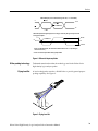
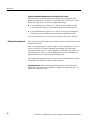
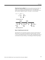
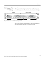
Figure 23 shows a footprint example where two pads use vias. Detail A describes
the recommended position of the via with respect to the pad.
See detail A
Max via dia 0.25
mm (0.010 in)
Dia 0.51 mm
(0.020 in)
0.04 mm
(0.002 in)
0.32 mm
(0.013 in)
Detail A
Scale 50.000
Figure 23: Optional Via-in-Pad placement recommendation
P69xx Series High-Density Logic Analyzer Probes Instruction Manual
33