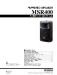
1
SERVICE MANUAL
CONTENTS
SPECIFICATIONS
................................................... 3
PANEL LAYOUT
.................................... 4
CIRCUIT BOARD LAYOUT
................. 5
BLOCK DIAGRAM
............................ 6
WIRING
..................................................................... 7
DISASSEMBLY PROCEDURE
.............................. 8
LSI PIN DESCRIPTION
.............................. 10
IC BLOCK DIAGRAM
................................. 14
CIRCUIT BOARDS
...................................... 16
TEST PROGRAM
............................ 21/31
MIDI DATA FORMAT
............... 40
MIDI INPLEMENTATION CHART .......................................... 44
PARTS LIST
OVERALL CIRCUIT DIAGRAM
SY 011470
19991101-168000
HAMAMATSU, JAPAN
1.58K-3711
Printed in Japan ’99.11
CS6X
IMPOR TANT NOTICE
This manual has been provided for the use of authorized Yamaha Retailers and their service personnel. It has been assumed
that basic service procedures inherent to the industry, and more specifically Yamaha Products, are already known and understood by the users, and have therefore not been restated.
WARNING :
Failure to follow appropriate service and safety procedures when servicing this product may result in personal injury, destruction of expensive components and failure of the product to perform as specified. For
these reasons, we advise all Yamaha product owners that all service required should be performed by an
authorized Yamaha Retailer or the appointed service representative.
IMPORTANT :
This presentation or sale of this manual to any individual or firm does not constitute authorization certification, recognition of any applicable technical capabilities, or establish a principal-agent relationship of
any form.
The data provided is belived to be accurate and applicable to the unit(s) indicated on the cover. The research engineering, and
service departments of Yamaha are continually striving to improve Yamaha products. Modifications are, therefore, inevitable
and changes in specification are subject to change without notice or obligation to retrofit. Should any discrepancy appear to
exist, please contact the distributor’s Service Division.
WARNING :
Static discharges can destroy expensive components. Discharge any static electricity your body may have
accumulated by grounding yourself to the ground bus in the unit (heavy gauge black wires connect to
this bus.)
IMPORTANT :
Turn the unit OFF during disassembly and parts replacement. Recheck all work before you apply power
to the unit.
LITHIUM BA TTER Y HANDLING
This product uses a lithium battery for memory back-up.
WARNING :
Lithium batteries are dangerous because they can be exploded by improper handling. Observe the following precautions when handling or replacing lithium batteries.
Leave lithium battery replacement to qualified service personnel.
Always replace with batteries of the same type.
When installing on the PC board by soldering, solder using the connection terminals provided on the battery cells.
Never solder directly to the cells. Perform the soldering as quickly as possible.
Never reverse the battery polarities when installing.
Do not short the batteries.
Do not attempt to recharge these batteries.
Do not disasemble the batteries.
Never heat batteries or throw them into fire.
ADVARSEL!
Lithiumbatteri-Eksplosionsfare ved fejlagtig handtering. Udskiftning ma kun ske med batteri af samme fabrikat og type. lever det brugte
batteri tilbage til leverandren.
VARNING
Explosionsfara vid felaktigt batteribyte.
Anvand samma batterityp eller en ekvivalent typ som rekommenderas av apparattillverkaren.
Kassera anvant batteri enligt fabrikantens instruktion.
VAROITUS
Paristo voi rajahtaa, jos se on virheellisesti asennettu.
Vaihda paristo ainoastaan laitevalmistajan suosittelemaan tyyppiiin.
Havita kaytetty paristo valmistajan ohjeiden mukaisesti.
The following information complies with Dutch official Gazette 1995. 45; ESSENTIALS OF ORDER ON THE COLLECTION OF BATTERIES.
• Please refer to the diassembly procedure for the removal of Back-up Battery.
• Leest u voor het verwijderen van de backup batterij deze beschrijving.
WARNING: CHEMICAL CONTENT NOTICE!
The solder used in the production of this product contains LEAD. In addition, other electrical/electronic and/or plastic (Where
applicable) components may also contain traces of chemicals found by the California Health and Welfare Agency (and possibly
other entities) to cause cancer and/or birth defects or other reproductive harm.
DO NOT PLACE SOLDER, ELECTRICAL/ELECTRONIC OR PLASTIC COMPONENTS IN YOUR MOUTH FOR ANY REASON WHAT
SO EVER!
Avoid prolonged, unprotected contact between solder and your skin! When soldering, do not inhale solder fumes or expose
eyes to solder/flux vapor!
If you come in contact with solder or components located inside the enclosure of this product, wash your hands before handling
food.
WARNING
Components having special characteristics are marked
originally installed.
2
and must be replaced with parts having specification equal to those
CS6X
SPECIFICATIONS
CS6x
KEYBOARD
Number of Keys
Touch
TONE GENERATION SYSTEM Tone Generators
Polyphony
VOICE
Number of Voice
61
Initial touch, Aftertouch
AWM2, Phrase Clip, Modular Synthesis Plug-in System
64
Normal voices (256 Presets, 128 Internals [Users], 128 Externals [Memory Cards]),
Drum voices (8 presets, 2 Internals [Users], 2 Externals [Memory Cards]), Plug-in voices (64 x 2 Plug-in Boards [If installed])
Wave ROM
PERFORMANCE
Multi-Timbres
Number of Performance
Master Keyboard Mode
PHRASE CLIP
Number of Clip
Number of Clip Kits
Sampling
EFFECT
128 Internals, 64 Externals
4 Zones
256 (Max)
4 (73 Keys [C0-C6] x 4 Kits)
16 bits linear, 44.1 kHz
Memory
4 Mbyte (DRAM)
Reverb
12
Chorus
Insertion
SCENE
SEQUENCE PLAY
16 MByte
20 (16 Voice Parts, Phrase Clip Part, A/D Input Part, Plug-in 1/2 Parts)
23
24 (Insertion 1), 92 (Insertion 2), 24 (Insertion for Plug-in Voices)
Scene 1/2, Scene Control, Scene Store
Format
Number of Sequence Chains
ARPEGGIATOR
Number of Arpebbios
Card
File Type
Functions
CONTROLS
SMF Format 0 (Direct Play only), Sequence Chain (Load/Save)
100 Steps (100 Songs)
128
All Data, All Voice Data, All Phrase Clip Data, Plug-in, Sequence Chain, SMF, WAV, AIFF
Save, Load, Rename, Delete, Make Directory, Format
Volume Knob, Octave Up/Down (CS6x), Pitch (CS6x), Modulation (CS6x), Ribbon Controller (CS6x), Scene 1, 2 (CS6x), Scene Control (CS6x),
2 Filter Knobs (CS6x), 2 Effect Knobs (CS6x), 4 EG Knobs (CS6x), Pan Knob (CS6x), Portamento ON/OFF (CS6x), Arpeggio Gate Time (CS6x),
Arpeggio Hold (CS6x), Arpeggio ON/OFF (CS6x), Phrase Clip Pitch (CS6x), Phrase Clip, Phrase Clip Rec, Tempo (CS6x), Sequence Play,
Sequence PLAY/STOP, Shift, Page, Knob A/B/C/1/2, Data, Effect Bypass, Master Keyboard (CS6x), Exit, Enter Dec/No, Inc/Yes, 7 Mode Keys,
6 Memory Keys, 8 Bank Keys (CS6x), 16 Program/Part Keys (CS6x), Power, Card Slot, Gain, Host Select
CONNECTORS & TERMINALS
MIDI In, Out, Thru, To Host, Breath, Footswitch (CS6x), Sustain (CS6x), Foot Controller (CS6x), Foot Volume (CS6x), Individual Output 1, 2,
Output L/Mono R, Phones, A/D Input (LINE 1, MIC/LINE 2), AC Inlet, 2 Connectors for Plug-in Boards
DISPLAY
40 x 2 (Backlit)
INCLUDED ACCESSORIES
Owner's Manual, Data List , Memory Card, CD-ROM, AC Power Cord
OPTIONAL ACCESSORIES
PLG150 Plug-in Boards Series, PLG100 Plug-in Boards Series,
FC4/5 Footswitch, FC7 Foot Controller, BC3 Breath Controller
POWER CONSUMPTION
OUTPUT IMPEDANCE
DIMENSIONS
WEIGHT
16watts
Output: +18.1 ±2dbm (10k ohms), Phones: +17.2 ±2dbm (33 ohms)
1019(W) x 357(D) x 109(H) mm
11.6 kg
3
CS6X
PANEL LAYOUT
Front panel
1
GAIN
MIC/LINE 2
6
LINE 1
A / D INPUT
L/MONO
PHONES
VOLUME
R
OUTPUT
7
1
2
FOOT
FOOT
FOOT
INDIVIDUAL OUTPUT VOLUME CONTROLLER SUSTAIN SWITCH
FILTER
IN
BREATH
TO HOST
9 10
OUT
HOST SELECT
8
12 15 13 14 16 19
THRU
3.3V CARD
MIDI
POWER
EFFECT
MEMORY
MODE
PORTAMENTO
CUTOFF
RESONANCE
REVERB
PHRASE CLIP
2
CARD
EXIT
PITCH
SEQ PLAY
ATTACK
UP
UTILITY
EF
BYPASS
MASTER
KEYBOARD
PRE1
PRE2
A
DECAY
SCENE
1
SUSTAIN
PAN
EDIT
RELEASE
JOB
SYSTEM
A
B
C
1
ENTER
D
E
4
1
F
TEMPO
VEL RATE
INT
EXT
1
2
3
4
5
6
GENERAL
QED
ARPEGGIO
CONTROL
COM LFO
EFFECT
9
10
11
12
13
OSC
PITCH
FILTER
AMPLITUDE
LFO
DRUM
PLG1
PLG2
14
15
16
EQ
PLG
COMPARE
STORE
SHIFT
PAGE
PART/ELEMENT
5
DATA
17 18
11
Rear panel
3
3.3V
POWER
ON
OFF
5 6 7 8 9
4
CARD
THRU
AC INLET
MIDI
OUT
IN
HOST SELECT
TO HOST
BREATH
FOOT
SWITCH
FOOT
FOOT INDIVIDUAL OUTPUT
1
2
SUSTAIN CONTROLLER VOLUME
R
OUTPUT
L MONO PHONES
A D INPUT
LINE 1 MIC LINE 2
GAIN
MIDI
Mac
PC-2 PC-1
10 11 12
1
2
3
4
5
6
7
8
4
POWER switch
AC INLET terminal
CARD slot
MIDI IN, OUT, and THRU connectors
HOST SELECT switch
TO HOST terminal
BREATH jack
FOOT SWITCH jack
9
10
11
12
13
14
15
16
SUSTAIN jack
FOOT CONTROLLER jack
FOOT VOLUME jack
INDIVIDUAL OUTPUT 1 and 2 jacks
OUTPUT L/MONO and R jack
PHONES jack
A/D INPUT jack
GAIN knob
BANK
20
PROGRAM
PART
21
4
8
3
2
H
7
4
1
G
2
3
ELEMENT ON/OFF
2
DEC/NO INC/YES
PLAY/
STOP
ON/
OFF
HOLD
PAN
C
2
3
ELEMENT SELECT
CURSOR
ARPEGGIO
2
CONTROL
B
1
DRUM
REC
ON/
OFF
DOWN
PERFORM
CHORUS
EG
OCTAVE
VOICE
13 14 15 16
1
2
3
4
5
6
7
8
9
10
11
12
13
14
15
16
17
18
19
20
21
[VOLUME] knob
OCTAVE [UP] and [DOWN] keys
PITCH bend wheel
MODULATION wheel
Ribbon control
Sound Control knobs
MODE keys
LCD (Liquid Crystal Display)
[SHIFT] key
[PAGE] knob
Knobs [A],[B],[C],[1] and [2]
[DATA] knob
[EF BYPASS] key
[MASTER KEYBOARD] key
[EXIT] key
[ENTER] key
[DEC/NO] key
[INC/YES] key
MEMORY keys
BANK [A] to [H] keys
PROGRAM/PART [1] to [16] keys
CS6X
CIRCUIT BOARD LAYOUT
RIB
DM
PNA
RV
PNB
PS
LCD
JK
SM
5
CS6X
BLOCK DIAGRAM
28CA1-8813234
6
CS6X
WIRING
7
CS6X
DISASSEMBLY PROCEDURE
1.
Bottom Assembly
Remove the thirty-five (35) screws marked [104], the
two (2) corner plates, marked [102], and the two (2)
coin screws marked [106]. The botton assembly can
then be removed.
SM, RV, Display Ass'y
[104]
〈BOTTOM VIEW〉
Circuit Board & Unit
Ref No.
PARTS NAME
PARTS No.
Q'ty
Fig.
PLG Support Brecket
112
Bind Head Tapping Screw-B 3.0 X 6 MFZN2BL
EP600230
5
2
SM
62
Bind Head Tapping Screw-B 3.0 X 8 MFZN2BL
EP600190
2
2
JK
322
Bonding Tapping Screw-B 3.0 X 10 MFZN2BL
VQ049800
9
2
DM
122
Bind Head Tapping Screw-B 3.0 X 6 MFZN2BL
EP600230
7
3
Remove the DM circuit board with the DM sheeld plate.
RV
52
Bind Head Tapping Screw-B 3.0 X 6 MFZN2BL
EP600230
8
4
Display Ass'y
22
Bind Head Tapping Screw-B 3.0 X 6 MFZN2BL
EP600230
4
4
PARTS NAME
PARTS No.
Q'ty
Fig.
PNB
Circuit Board & Unit
[102]
[106]
[102]
Ref No.
PS Ass'y
92
Bind Head Tapping Screw-B 3.0 X 6 MFZN2BL
EP600230
6
2
PLG Support Brecket
112
Bind Head Tapping Screw-B 3.0 X 6 MFZN2BL
EP600230
5
2
SM
62
Bind Head Tapping Screw-B 3.0 X 8 MFZN2BL
EP600190
2
2
PNB
42
Bind Head Tapping Screw-B 3.0 X 8 MFZN2BL
EP600190
11
4
Fig.1
[102]: Coner Plate (V4196900)
[104]: Bind Head Tapping Screw-B 3.0X8 MFZN2BL (EP600190)
[106]: Screw 3.0X6 (V2517100)
2.
[62]
Circuit Boards and Units
After removing the bottom assembly, remove the
circuit board and unit, following the procedure in the
below table.
[72]
[72]
[42]
[72]
[72]
KEYBOARD
DM
Circuit Board & Unit
Ref No.
PARTS NAME
PARTS No.
Q'ty
Fig.
KEYBOARD Ass'y
Touch Volume
72
Bind Head Tapping Screw-B 3.0 X 6 MFZN2BL
EP600230
4
2
62
Bind Head Tapping Screw-B 3.0 X 8 MFZN2BL
EP600190
4
2
Wheel Ass'y
42
Bind Head Tapping Screw-B 3.0 X 8 MFZN2BL
EP600290
4
2
PS Ass'y
92
Bind Head Tapping Screw-B 3.0 X 6 MFZN2BL
EP600230
6
2
PS
JK
〈REAR VIEW〉
[322]
[62]
JK, DM, PNA
Circuit Board & Unit
PARTS NAME
PARTS No.
Q'ty
Fig.
JK
Ref No.
322
Bonding Tapping Screw-B 3.0 X 10 MFZN2BL
VQ049800
9
2
DM
122
Bind Head Tapping Screw-B 3.0 X 6 MFZN2BL
EP600230
7
3
EP600230
11
4
Remove the DM circuit board with the DM sheeld plate.
PNA
8
32
Bind Head Tapping Screw-B 3.0 X 10 MFZN2BL
[92]
[112]
[322]
Fig.2
[92]
[92]
CS6X
DM
[122]
[122]
Fig.3
[32]
[52]
[42]
RV
PNB
PNA
LCD Assy
SM
[22]
Fig.4
3.
3-1
3-2
Keyboard Assembly
Remove the bottom assembly. (See Procedure 1.)
Remove the four(4) screws marked [72].
The keyboard Assembly can then be removed.(Fig.2)
9
CS6X
LSI PIN DESCRIPTION
HD64F7045F28 (XW419A00) CPU
PIN
NAME
I/O
FUNCTION
NO.
1
2
3
4
5
6
7
8
9
10
11
12
13
14
15
16
17
18
19
20
21
22
23
24
25
26
27
28
29
30
31
32
33
34
35
36
37
38
39
40
41
42
43
44
45
46
47
48
49
50
51
52
53
54
55
56
57
58
59
60
61
62
63
64
65
66
67
68
69
70
71
72
10
/WRHH
PE14
/WRHL
PA21
PE15
VSS6
A0
A1
A2
A3
A4
VCC12
A5
VSS14
A6
A7
A8
A9
A10
A11
A12
A13
A14
A15
A16
VCC26
A17
VSS28
PA20
PA19
PB2
PB3
PA18
PB4
VSS35
PB5
A18
A19
A20
VCC40
A21
VSS42
/RD
/WDTOVF
D31
D30
/WRH
WRL
/CS1
CS0
PA9
PA8
/CS3
/CS2
VSS55
D29
D28
D27
D26
D25
VSS61
D24
VCC63
D23
D22
D21
D20
D19
D18
D17
VSS71
D16
O
I/O
O
I
I/O
O
O
O
O
O
O
O
O
O
O
O
O
O
O
O
O
O
O
I
I
O
O
I
O
O
O
O
O
O
O
I/O
I/O
O
O
O
O
I
I
O
O
—
I/O
I/O
I/O
I/O
I/O
I/O
I/O
I/O
I/O
I/O
I/O
I/O
I/O
I/O
HH write
LCD data 6 input / output
MLAN insert detect
LCD data 7 input / output
Ground
Address bus
Power supply
Address bus
Ground
Address bus
Power supply
Address bus
Ground
Encoder 2A input
Encoder 2B input
Row address strobe
Column address strobe (low)
Host off line detect input
Column address strobe (high)
Ground
DRAM read/write
Address bus
Power supply
Address bus
Ground
Read
Not used
Data bus
High write
Low write
Chip Select 1
Chip Select 0
MLAN MIDI interrupt request
Interrupt request
Chip select 3
Chip select 2
Ground
Data bus
Ground
Data bus
Power supply
Data bus
Ground
Data bus
PIN
NO.
73
74
75
76
77
78
79
80
81
82
83
84
85
86
87
88
89
90
91
92
93
94
95
96
97
98
99
100
101
102
103
104
105
106
107
108
109
110
111
112
113
114
115
116
117
118
119
120
121
122
123
124
125
126
127
128
129
130
131
132
133
134
135
136
137
138
139
140
141
142
143
144
NAME
D15
D14
D13
D12
VCC77
D11
VSS79
D10
D9
D8
D7
D6
VCC85
D5
VSS87
D4
D3
D2
D1
D0
VSS93
XTAL
MD3
EXTAL
MD2
NMI
VCC99/FWP99
PA16
PA17
MD1
MD0
PLLVCC
PLLCAP
PLLVSS
PA15
/RES
TIOCOA
PE1
PE2
VCC112
PE3
PE4
PE5
PE6
VSS117
AN0
AN1
AN2
AN3
AN4
AN5
AVSS
AN6
AN7
AVREF
AVCC
VSS129
RXD0
TXD0
/IRQ0
RXD1
TXD1
VCC135
/IRQ1
PE7
PE8
PE9
PE10
VSS141
PE11
PE12
PE13
I/O
I/O
I/O
I/O
I/O
I/O
I/O
I/O
I/O
I/O
I/O
I/O
I/O
I/O
I/O
I/O
I/O
I
I
I
I
I
I
I
I
O
I
I
I
I
I
O
I
I
I
I
I
I
I
I
I
I
O
I
I
O
I
I
I/O
I/O
I/O
I/O
I/O
I/O
FUNCTION
Data bus
Power supply
Data bus
Ground
Data bus
Power supply
Data bus
Ground
Data bus
Ground
Crystal oscillator
Mode select
Crystal oscillator
Mode select
Non-maskable interrupt
Power supply
Encoder 1B input
Encoder 1A input
Mode select
Mode select
PLL power supply
PLL capacitor
PLL ground
CPU clock out
Reset
A/D jack insert detect interrupt request input
Smart MINS
Model detection
Power supply
Smart busy input
MLAN reset interrupt request input
1M clock out
Model detection
Ground
Analog input
Analog ground
Analog input
Analog reference voltage
Analog power supply
Ground
MIDI input
MIDI output
Plug in sireal interrupt request input
HOST input
HOST output
Power supply
MLAN MIDI interrupt input
Smart Vprt Input
LCD data 0 input / output
LCD data 1 input / output
LCD data 2 input / output
Ground
LCD data 3 input / output
LCD data 4 input / output
LCD data 5 input / output
CS6X
HD63B01Y0RCE0F (XM234A00) CPU (PKS)
PIN
NO.
1
2
3
4
5
6
7
8
9
10
11
12
13
14
15
16
17
18
19
20
21
22
23
24
25
26
27
28
29
30
31
32
NAME
/NMI
E
D#
D
C#
CL
PULL 1
PULL 2
LC.AE//FS
/REPEAT
/KOF-REQ
SW1
SW2
/IS
/OS
SW3
SW4
DOUT0
DOUT1
DOUT2
DOUT3
DOUT4
DOUT5
DOUT6
DOUT7
Vcc
Sf
M5/S13
M4/S12
M3/S10
M2/S9
M1/S8
I/O
I
O
O
O
O
O
I
I
I
I
I
I
I
I
I
O
O
O
O
O
O
O
O
O
I
I
I
I
I
FUNCTION
Non-maskable interrupt
Key scan drive
connected to ground
Auto repeat (L:on, H:off)
Key off request
Switch 1 (L: on, H: off)
Switch 2 (L: on, H: off)
Input strobe
Output strobe
Switch 3 (L: on, H: off)
Switch 4 (L: on, H: off)
Data output
Power supply (+5V)
Switch drive
Make contact of key receive/
Switch receive
PIN
NO.
33
34
35
36
37
38
39
40
41
42
43
44
45
46
47
48
49
50
51
52
53
54
55
56
57
58
59
60
61
62
63
64
NAME
M1/S8
M0/S7
Vss
F
F#
G
G#
A
A#
B
C
LC//AE
B6/S6
B5/S5
B4/S4
B3/S3
B2/S2
B1/S1
B0/S0
Se
Sd
Sc
Sb
Sa
E
Vss
XTAL
EXTAL
MP0
MP1
/RES
/STBY
I/O
I
I
O
O
O
O
O
O
O
O
I
I
I
I
I
I
I
I
O
O
O
O
O
I
I
I
I
I
FUNCTION
Make contact of key receive/
Switch receive
Ground
Key scan drive
connected to +5V
Break contact of key receive/
Switch receive
Switch drive
Not used
Ground
Not used
8 MHz clock
Mode program 0
Mode program 1
Initial clear
Stanby-mode signal
µ PD63200GS (XM145A00) DAC (Digital to Analog Converter)
PIN
NO.
1
2
3
4
5
6
7
8
NAME
4/8F
D. GND
16 BIT
D. VDD
A. GND
R. OUT
A. VDD
A. VDD
I/O
I
I
O
FUNCTION
4/8 Fs selection
Digital ground
16 bit/18 bit selection
Digital power supply
Analog ground
Channel R output
Analog power supply
PIN
NO.
9
10
11
12
13
14
15
16
NAME
R. REF
L. REF
L. OUT
A. GND
WDCK
RSI
SI/LSI
CLK
I/O
O
I
I
I
I
FUNCTION
Channel R voltage reference
Channel L voltage reference
Channel L output
Analog ground
Word clock
Channel R series input
Series input/Channel L series nput
Clock
JG710069 (XM326B00) DDE1 (DAC Dynamic Range Enhancer)
PIN
NO.
1
2
3
4
5
6
7
8
NAME
I/O
CLK
SYW
MIN 1
MIN 0
Vss
SEL 1
SEL 0
SUP
I
I
I
I
I
I
I
FUNCTION
Master clock
Sync signal
Signal input
Signal input
Ground
Mode select
Mode select
1 bit shift up input
PIN
NO.
9
10
11
12
13
14
15
16
NAME
I/O
SH 0
SH 1
LE
V DD
DACO 0
DACO 1
DCLK
ICN
O
O
O
O
O
O
I
FUNCTION
N.C.
N.C.
Latch enable for DAC
Power supply
Output (DAC)
Output (DAC)
Clock for DAC
Initial clear
11
CS6X
TC203C760HF-002 (XS725A00) SWP30B AWM Tone Generator coped with MEG) Standard Wave Processor
12
PIN
NO.
NAME
1
2
3
4
5
6
7
8
9
10
11
12
13
14
15
16
17
18
19
20
21
22
23
24
25
26
27
28
29
30
31
32
33
34
35
36
37
38
39
40
41
42
43
44
45
46
47
48
49
50
51
52
53
54
55
56
57
58
59
60
61
62
63
64
65
66
67
68
69
70
71
72
73
74
75
76
77
78
79
80
81
82
83
84
85
86
87
88
89
90
91
92
93
94
95
96
97
98
99
100
101
102
103
104
105
106
107
108
109
110
111
112
113
114
115
116
117
118
119
120
Vss
CA0
CA1
CA2
CA3
CA4
CA5
CA6
CA7
CA8
CA9
CA10
CA11
VSS
CD0
CD1
CD2
CD3
CD4
CD5
CD6
CD7
CD8
CD9
CD10
CD11
CD12
CD13
CD14
VDD
VSS
CD15
CSN
WRN
RDN
VDD
SYSH0
SYSH1
SYSH2
SYSH3
SYSH4
SYSH5
SYSH6
SYSH7
KONO0
KONO1
KONO2
KONO3
VSS
SYSL0
SYSL1
SYSL2
SYSL3
SYSL4
SYSL5
SYSL6
SYSL7
KONI0
KONI1
VDD
VSS
KONI2
KONI3
DAC0
DAC1
WCLK
MELO0
MELO1
MELO2
MELO3
MELO4
MELO5
MELO6
MELO7
VDD
ADLR
MELI0
MELI1
MELI2
MELI3
MELI4
MELI5
MELI6
MELI7
VSS
RCASN
RA8
RA7
RA6
VDD
VSS
RA5
RA4
RA3
RA2
RA1
RA0
RRASN
RWEN
VSS
RD7
RD6
RD5
RD4
RD3
RD2
RD1
RD0
VSS
RD17
RD16
RD15
RD14
RD13
RD12
RD11
RD10
RD9
RD8
VDD
I/O
FUNCTION
(Ground)
I
I
I
I
I
I
I
I
I
I
I
I
Address bus of internal register
(Ground)
I/O
I/O
I/O
I/O
I/O
I/O
I/O
I/O
I/O
I/O
I/O
I/O
I/O
I/O
I/O
Data bus of internal register
(Power supply)
(Ground)
I/O
I
I
I
Chip select
Write strobe
Read strobe
(Power supply)
O
O
O
O
O
O
O
O
O
O
O
O
NSYS/LNSYS upper 16 bits output
Key on data
(Ground)
I/O
I/O
I/O
I/O
I/O
I/O
I/O
I/O
I
I
I
I
I
O
O
O
O
O
O
O
O
O
O
O
NSYS input/LNSYS output lower 8 bits
Key on data input
(Power supply)
(Ground)
DAC output
DAC0/DAC1 word clock
MEL wave data output
(Power supply)
O
I
I
I
I
I
I
I
I
O
O
O
O
O
O
O
O
O
O
O
O
ADC word clock
MEL wave data input
(Ground)
DRAM column address strobe (RAS signal)
(Power supply)
(Ground)
DRAM address bus
DRAM row address strobe (RAS signal)
DARM write enable
(Ground)
I/O
I/O
I/O
I/O
I/O
I/O
I/O
I/O
(Ground)
I/O
I/O
I/O
I/O
I/O
I/O
I/O
I/O
I/O
I/O
DRAM data bus
(Power supply)
PIN
NO.
121
122
123
124
125
126
127
128
129
130
131
132
133
134
135
136
137
138
139
140
141
142
143
144
145
146
147
148
149
150
151
152
153
154
155
156
157
158
159
160
161
162
163
164
165
166
167
168
169
170
171
172
173
174
175
176
177
178
179
180
181
182
183
184
185
186
187
188
189
190
191
192
193
194
195
196
197
198
199
200
201
202
203
204
205
206
207
208
209
210
211
212
213
214
215
216
217
218
219
220
221
222
223
224
225
226
227
228
229
230
231
232
233
234
235
236
237
238
239
240
NAME
VSS
HMD0
HMD1
HMD2
HMD3
HMD4
HMD5
HMD6
HMD7
HMD8
HMD9
HMD10
HMD11
HMD12
HMD13
HMD14
HMD15
VSS
HMA0
HMA1
HMA2
HMA3
HMA4
HMA5
HMA6
HMA7
HMA8
HMA9
HMA10
VDD
VSS
HMA11
HMA12
HMA13
HMA14
HMA15
HMA16
HMA17
HMA18
HMA19
HMA20
HMA21
HMA22
HMA23
HMA24
VSS
MRASN
MCASN
MOEN
MWEN
VSS
LMD0
LMD1
LMD2
LMD3
LMD4
LMD5
LMD6
LMD7
VDD
VSS
LMD8
LMD9
LMD10
LMD11
LMD12
LMD13
LMD14
LMD15
VSS
LMA0
LMA1
LMA2
LMA3
LMA4
LMA5
LMA6
LMA7
LMA8
LMA9
LMA10
LMA11
VSS
LMA12
LMA13
LMA14
LMA15
LMA16
LMA17
VDD
VSS
LMA18
LMA19
LMA20
LMA21
LMA22
LMA23
LMA24
VSS
SYO
SYOD
QCLK
HCLK
CK256
SYSCLK
VDD
SYI
MCLKI
MCLKO
VDD
XIN
XOUT
VSS
ICN
CHIP2
SLAVE
TESTON
ACIN
DCTEST
VDD
I/O
FUNCTION
(Ground)
I/O
I/O
I/O
I/O
I/O
I/O
I/O
I/O
I/O
I/O
I/O
I/O
I/O
I/O
I/O
I/O
Wave memory data bus (Upper 16 bits)
(Ground)
O
O
O
O
O
O
O
O
O
O
O
(Power supply)
(Ground)
O
O
O
O
O
O
O
O
O
O
O
O
O
O
Wave memory address bus
(Ground)
O
O
O
O
I/O
I/O
I/O
I/O
I/O
I/O
I/O
I/O
RAS when DRAM(s) is connected to wave memory
CAS when DRAM(s) is connected to wave memory
Wave memory output enable
Wave memory write enable
(Ground)
Wave memory data bus (Lower 16 bits)
(Power supply)
(Ground)
I/O
I/O
I/O
I/O
I/O
I/O
I/O
I/O
(Ground)
O
O
O
O
O
O
O
O
O
O
O
O
(Ground)
O
O
O
O
O
O
Wave memory address bus (Lower data memory)
(Power supply)
(Ground)
O
O
O
O
O
O
O
O
O
O
O
O
O
I
I
O
I
O
I
I
I
I
I
I
(Ground)
Sync. signal for master clock
Sync. signal for HCLK/QCLK
1/12 master clock (64Fs)
1/6 master clock (128Fs)
1/3 master clock (256Fs)
1/2 master clock (384Fs)
(Power supply)
Sync. clock
Master clock input
Master clock output
(Power supply)
Crystal osc. input
Crystal osc. output
(Ground)
Initial clear
2 chips mode enable
Master/Slave select when 2 chips mode
Test pin
(Power supply)
CS6X
MN101C027YB (XS711200) CPU
PIN
NO.
1
2
3
4
5
6
7
8
9
10
11
12
13
14
15
16
17
18
19
20
21
22
23
24
25
26
27
28
29
30
31
32
NAME
I/O
S1
S2
S3
S4
S5
VREF+
VDD
OSC2
OSC1
VSS
XI
XO
MMOD
RD0
RXD
D0
D1
D2
D3
D4
/RST
D5
D6
D7
D8
D9
S6
S7
S8
S9
S10
S11
I
I
I
I
I
O
I
I
O
I
O
I
O
O
O
O
O
I
O
O
O
O
O
I
I
I
I
I
I
FUNCTION
Switch matrix data
Power supply (+5V, analog)
Power supply (+5V)
Crystal oscillator (8MHz)
Crystal oscillator (8MHz)
Ground
Not used
Not used
Memory mode select (Grounded)
Rotary encoder data
MIDI receive data
LED and switch drive data
Reset
LED and switch drive data
Switch matrix data
PIN
NO.
33
34
35
36
37
38
39
40
41
42
43
44
45
46
47
48
49
50
51
52
53
54
55
56
57
58
59
60
61
62
63
64
NAME
I/O
S12
S13
S14
TXD
S15
S16
S17
S18
L16
L17
L18
L19
L8
L9
L10
L11
L12
L13
L14
L15
L7
L6
L5
L4
L3
L2
L1
L0
VREF
AD0
AD1
S0
I
I
I
O
I
I
I
I
O
O
O
O
O
O
O
O
O
O
O
O
O
O
O
O
O
O
O
O
I
I
I
FUNCTION
Switch matrix data
MIDI transmit data
Switch matrix data
LED drive data
LED and switch drive data
Grounded
Analog input
Analog input
Switch matrix data
MBCG46183-129 (XV833A00) Gate Array
PIN
NO
NAME
I/O
1
2
3
4
5
6
7
8
9
10
11
12
13
14
15
16
17
18
19
20
21
22
23
24
D5
D6
D7
/IRQ0
/IRQ1
VSS
/IRQ2
/IRQ3
/RD
/WR
/CE
/ASTB
TESTSIO
RX0
TX0
RX1
TX1
VSS
VDD
RX2
TX2/BO2
RX30
TX30
RX31
I/O
I/O
I/O
I/O
I/O
I/O
I/O
I
I
I
I
I
I
O
I
O
I
O
I
O
I
FUNCTION
Data Bus
Interrupt Request Port 0
Interrupt Request Port 1
Ground
Interrupt Request Port 2
Interrupt Request Port 3
Read Signal Input
Write Signal Input
Chip Enable Input
Address Strobe (Not used: to ground)
Input with Pull-down Resistor (50k)
Receive Data 0
Transmit Data 0
Receive Data 1
Transmit Data 1
Ground
Power Supply
Receive Data 2
Transmit Data 2
Receive Data 30
Transmit Data 30
Receive Data 31
PIN
NO
NAME
I/O
25
26
27
28
29
30
31
32
33
34
35
36
37
38
39
40
41
42
43
44
45
46
47
48
TX31
RX32
TX32
RX33
TX33
/IC
VSS
XI
VSS
XO
A0
A1
A2
A3
A4
A5
CPUCLK
VSS
VDD
D0
D1
D2
D3
D4
O
I
O
I
I/O
I
I
I/O
I
I
I
I
I
I
I
I/O
I/O
I/O
I/O
I/O
FUNCTION
Transmit Data 31
Receive Data 32
Transmit Data 32
Receive Data 33
Transmit Data 33
Initial Clear
Ground
Quartz Crystal Input
Ground
Quartz Crystal Output
Address Bus
CPU Clock
Ground
Power Supply
Data Bus
13
CS6X
PCM1800 (XU770A00) A/D Converter
PIN
NAME
I/O
FUNCTION
NO.
1
2
3
4
5
6
7
8
9
10
11
12
VINL
VREF1
REFCOM
VREF2
VINR
RSTB
BYPAS
FMT0
FMT1
MODE0
MODE1
FSYNC
I
I
I
I
I
I
I
I
I/O
Analog input (L ch.)
Reference 1 decoupling cap.
Reference decoupling common
Reference 2 decoupling cap.
Analog input (R ch.)
Reset input active “L”
LCF bypass control
Audio data format 0
Audio data format 1
Master/Slave mode selection 0
Master/Slave mode selection 1
Frame sync. input/output
PIN
NO.
NAME
I/O
13
14
15
16
17
18
19
20
21
22
23
24
LRCK
BCK
DOUT
SYSCK
DGND
VDD
CINNR
CINPR
CINNL
CINPL
VCC
AGND
I/O
I/O
O
I
-
FUNCTION
Sampling clock input/output
Bit clock input/output
Audio data output
System clock input
Digital ground
Power supply +5V
Anti-aliasing filter cap. (-) R ch.
Anti-aliasing filter cap. (+) R ch.
Anti-aliasing filter cap. (-) L ch.
Anti-aliasing filter cap. (+) L ch.
Analog power supply
Analog ground
IC BLOCK DIAGRAM
TC74VHC00F(XT229A00)
IC73
MAND
1A
14
1
2
13
4B
1Y
3
12
4A
4
11
1A
1
14
VDD
1Y
2
13
6A
2A
3
12
6Y
2Y
4
11
5A
VDD
1B
2A
TC74VH04F (XM332A00)
IC54
Inverter
4Y
3A
2B
5
10
6
9
7
8
1
1A
2
1B
3
1Y0
4
1Y1
1Y2
14
5
6
1Y3
7
GND
8
G
A
B
Y0
Y1
Y2
Y3
6
9
4A
7
8
4Y
3Y
TC74LVC139FPEL(XS048A00)
IC26, IC42
Demultiplexer
1G
5Y
3A
Vss
Vss
10
3B
3Y
2Y
5
TC74VHC157FF(XN966A00)
IC103
Multiplexer
TC74VH32F(XN963A00)
IC29, IC55
OR
1A
1
14
VCC
1B
2
13
4B
1Y
3
12
4A
2A
4
11
4Y
2B
5
10
3B
2Y
6
9
3A
GND
7
8
3Y
TC74VHC244F(XT800A00)
IC51
Bus Buffer
16
Vcc
1G
1
16
Vcc
1G
1
20
VDD (Vcc)
G
15
2G
1A
2
15
2G
1A1
2
19
2G
A
14
2A
1B
3
14
2A
2Y4
3
18
1Y1
1Y0
4
13
2B
1A2
4
17
2A4
5
12
2Y0
2Y3
5
16
1Y2
B
13
2B
Y0
12
2Y0
1Y1
Y1
11
2Y1
1Y2
6
11
2Y1
1A3
6
15
2A3
Y2
Y3
10
2Y2
1Y3
7
10
2Y2
2Y2
7
14
1Y3
2Y3
GND
8
9
2Y3
1A4
8
13
2A2
2Y1
9
12
1Y4
(GND) Vss
10
11
2A1
9
CS6X
1
VCC
20
IN / OUT
2
19
G
CLEAR
1
20
VCC
A2
3
18
B1
1Q
2
19
8Q
A3
4
17
B2
1D
3
18
8D
A4
5
16
B3
2D
4
17
7D
B4
2Q
5
16
7Q
6
2
GND
3
1CLR
1
1D
2
5
COUT
CK D
CL
Q
D CK
CL
Q
3Q
B5
6
A7
8
13
B6
3D
7
A8
9
12
B7
4D
8
GND
10
11
B8
4Q
9
Q
Q
CL
CK D
CL
D CK
M5M34051FP(XV103A00)
IC12
Line Transceiver
1
16
VCC
1A
2
15
1D
1R
3
14
1Y
1DE
4
13
1Z
2R
5
12
6D
13
5D
12
5Q
2DE
6
11
2Z
2A
Inverting
Input A
2B
7
10
2Y
Non-Inverting
Input A
GND
8
9
2D
Ground
SC7SU04FEL (XI348A00)
IC21
Inverter
NC
1
IN
2
VSS
3
6
VDD
5
OUT
CLOCK
NJM4556AMT1(XQ138A00)
IC23
Operation Amplifier
Output A
8
1
2
3
4
-
+
+
-
+DC Voltage
Supply
1
A1
2
A2
3
A3
4
A4
5
20
19
18
17
16
NJM4556AD (XQ824A00)
NJM4558D-V (IG001390)
µPC4570G2 (XF291A00)
µPC4570C (XC520A00)
IC62,IC65,IC68,IC74
Dual Operational Amplifier
Output A
1
7
Output B
Inverting
Input A
2
6
Inverting
Input B
Non-Inverting
Input A
3
5
Non-Inverting
Input B
-DC Voltage Supply
4
TC74VHCT245AF(XV242A00)
TC74VHCT245AFT(XT744A00)
SN74HC245NSR(XD838A00)
IC31,IC50
Buffer
Octo1 3-state Bus Transceiver
D1R
2PR
8
VCC
1B
2
7
1Y
2Y
3
6
2B
GND
4
OY
1
2Y
2
2Y
Y-COM
3
3Y
4
1Y
5
7
+V
-
+
+
-V
-
8
+DC Voltage
Supply
7
Output B
6
Inverting
Input B
5
Non-Inverting
Input B
PR
CLR
CLK
VDD
2X
15
2X
Y-COM 1X
14
1X
3Y
X-COM
13
X-COM
1Y
0X
12
OX
INH
3X
11
3X
A
10
A
9
B
5 2A
6
2Q
8
Q
16
2Q
9
6Q
14
11
2CK
1
TC74HC4052AF (XS790A00)
IC13,IC14,IC15,IC16
Multiplexer
INH
VEE
7
VSS
8
OUTPUTS
D
Q
Q
L
H
H
L
H
L
L
H
L
L
H
H
H
H
f
H
H
L
H
H
H
H
f
L
L
L
QO
H
QO
DS90C402M (XW357A00)
IC102
Line Receiver
Vcc
1
8
RI 2-
RO 1
2
7
RI 2+
RI 1+
3
6
RO 2
RI 1-
4
5
GND
R
1B
10
2D
10
Q
Q
R
GND
CK D
CL
Q
2CLR
11
PR
INPUTS
D CK
CL
Q
VCC
13
12
D
CK
Q
6
14
1A
PR
5
1Q
15
CK
4
1PR
GND
14
D
3
1CK
1Q
15
7
Q
CL
CK D
CL
D CK
OUT / IN
Vcc
4
TC7W32FU(TE12L) (XQ173A00)
IC75
OR
B
A6
Q
1
TC74HC74AF (XP003A00)
IC18,IC19
Dual D-Type Flip-Flop
0Y
A1
A5
TC7S66FF(XR682A00)
IC30
Analog Switch
CLR
D1R
TC74VHC273F(XN971A00)IC52
SN74HC273NSR(XH223A00)
IC27, IC28,IC52
D-FF
CLR
TC74VHC245F(XT487A00)
IC11,IC101
Transceiver
TC74HC14AF-TP1 (XD657A00)
IC8,IC17,IC20,IC22,IC32,IC100
Hex Inverter
1A
1
14
VDD
1Y
2
13
6A
2A
3
12
6Y
2Y
4
11
5A
3A
5
10
5Y
6
9
7
8
VCC
G
B1
B2
B3
3Y
A5
6
15
B4
A6
7
14
B5
A7
8
13
B6
A8
9
12
B7
GND
10
11
B8
GND
4A
4Y
15
CS6X
CIRCUIT BOARDS
DM Circuit Board
CN19: to PNA-CN1
CN22: to SM-CN1
CN20: to JK-CN2
CN18: OPTION-MLAN-CN1
CN21: to JK-CN4
CN6: to RV-CN10
CN7: to PNA-CN3
CN15: to PLUG IN1-CN1
CN4: to JK-CN5
CN16: to PLUG IN2-CN1
CN13:
CN12:
to LCD-2P to LCD-CN1
CN14:
to RV-CN11
CN17:
to PNA-CN4
CN3:
to LC-CN2
CN2:
to LC-CN3
CN11:
to PS-CN3
CN10:
CN9:
CN5:
CN8:
to KS-CN1 to RIB-CN14 to WHEEL-5P to JK-CN7
Component side
Note : See parts list for details of circuit board component parts.
DM: 2NA-V357640
16
1
CS6X
Pattern side
Battery VN103500
VN103600(Battery holder for VN103500)
• Notice for back-up battery removal
Push the battery as shows in figure,
then the battery will pop up.
• Druk de batterij naar beneden zoals
aangeven in de tekening, de batterij
springt dan naar voren.
17
CS6X
RIB Circuit Board
RV Circuit Board
CN15: from RIBBON
CN9: to PNA-CN8
CN10: to DM-CN6
CN11: to DM-CN14
CN14:
to DM-CN9
CN14: to DM-CN9
Component side
Component side
PNA Circuit Board
CN1:
CN2:
to DM-CN19 to JK-CN1
CN3: to DM-CN7
CN5: to PNB-CN12
CN6: to PNB-CN13
CN4: to DM-CN17
CN7:
CN8:
to JK-CN6 to RV-CN9
Component side
18
RIB, RV, PNA: 2NA-V357940
1
CS6X
PNB Circuit Board
CN12: to PNA-CN5
CN13: to PNA-CN6
Component side
SM Circuit Board
CN1: to DM-CN22
PNB: 2NA-V357980
SM: 2NA-V357710
1
1
Component side
Pattern side
19
CS6X
JK Circuit Board ( B virsion)
HOST SELECT
PC2 PC1
MIDI
THRU
OUT
IN
MIDI
to HOST
BREATH
FOOT
SWITCH
SUSTAIN
FOOT
FOOT
CONTROLLER VOLUME
INDIVIDUAL OUTPUT
2
Mac
1
OUTPUT
R
L/MONO
PHONES
A/D
INPUT
MIC/LINE2
LINE1
GAIN
CN4: to DM-CN21
CN5: to DM-CN4
CN6: to PNA-CN7
JK Circuit Board ( C virsion)
HOST SELECT
PC2 PC1
MIDI
THRU
OUT
CN7: to DM-CN8
IN
MIDI
to HOST
BREATH
FOOT
SWITCH
SUSTAIN
CN2: to DM-CN20
FOOT
FOOT
CONTROLLER VOLUME
CN1: to PNA-CN2 CN3: to PS-CN2
INDIVIDUAL OUTPUT
Mac
R
L
Component side
OUTPUT
R
L/MONO
PHONES
A/D
INPUT
MIC/LINE2
LINE1
GAIN
CN4: to DM-CN21
CN5: to DM-CN4
CN6: to PNA-CN7
CN7: to DM-CN8
CN2: to DM-CN20
CN1: to PNA-CN2 CN3: to PS-CN2
Component side
JK: 2NA-V357700
20
1
CS6X
TEST PROGRAM
Test No.
Test Conditions, Judgment Criteria, etc.
Test Item
T1
RAM READ/WRITE
OK/NG, (MAIN SRAM/WAVE DRAM)
T2
RAM BATTERY
OK/NG, 2.7V or more, Less than 3.5V
T3
WAVE ROM
OK/NG
T4
LCD
ON/OFF blinking alternately
T5
PANEL SWITCH/LED
OK/NG
T6
ENCODER
OK; 0 to +127(0) to -127
T7
KEYBOARD
OK, KEY CODE/KEY TOUCH
T8
KNOB A-2
OK/NG, 64-127-0-64
T10
KNOB 1-4
OK/NG, 64-127-0-64
T11
KNOB 5-14
OK/NG, 64-127-0-64
T12
CONTROLLER
OK/NG, 64-127-0-64 (PB), 0-127-0 (MW), 0-107-0 (AT)
T13
FOOT CONTROL SWITCH
OK, 0-127-0
T14
BREATH CONTROLLER
OK/NG, 127-0-127
T15
CARD
OK/NG
T16
MIDI IN/OUT/THRU
OK/NG THRU Confirmation
T17
HOST SELECT
OK/NG
T18
TO HOST
OK/NG
OUTPUT(L): +6.0 ± 2 dBm; OUTPUT(R): Less than -72.0 dBm (10 kohm load)
T19
1 kHz OUTPUT L
INDIV(1): +6.0 ± 2 dBm; INDIV(2): Less than-72.0 dBm (10 kohm load)
PHONES(L): +5.0 ± 2 dBm; PHONES(R): Less than -64.0 dBm (33 ohm load)
OUTPUT(L): Less than -72.0 dBm (10 kohm load); OUTPUT(R): +6.0 ± 2 dBm
T20
1 kHz OUTPUT R
INDIV(1): Less than -72.0 dBm (10 kohm load); INDIV(2): +6.0 ± 2 dBm
PHONES(L): Less than -64.0 dBm (33 ohm load); PHONES(R): +5.0 ± 2 dBm
T21
A/D LEVEL, JACK
OK
T22
A/D -> D/A
OUTPUT (L, R): +15.0 ± 2 dBm (Line) (10 kohm)
T23
PLUG- IN1
OUTPUT (L, R): +11.5 ± 2 dBm (10 kohm)
T24
PLUG- IN2
OUTPUT (L, R): +11.5 ± 2 dBm (10 kohm)
T25
mLAN
OK/NG
T26
FACTORY SET
OK/NG
T27
SWP CH
1 kHz, sine wave
T28
EXIT (NOISE LEVEL)
Initialized state
OUTPUT (L, R): Less than -82.0 dBm (10 kohm load)
PHONES (L, R): Less than -85.0 dBm (33 ohm load)
Measuring instruments: frequency counter, oscilloscope, AC voltmeter (JIS-C curve type), distortion meter
(with flat filter), keyboard amplifier, etc.
Jigs:
MIDI cable, specially designed expansion board, etc.
21
CS6X
A. HOW TO ENTER THE TEST PROGRAM
C. TEST SELECTION WHEN AN ERROR HAS BEEN DETECTED
While pressing the [VOICE], [PERFORM] and [STORE]
switches, turn on the [POWER ON/OFF] switch. The
following message will then appear.
When the test result has been judged as “NG” in each of
the following tests, choose whether to execute the same
test or to proceed to the next test.
In this state, pressing the [EXIT] switch will cancel the
test mode and restore the normal state.
AUTO MODE:
Press the [EXIT] switch to set to the error processing state.
MANUAL MODE:
Press the [EXIT] switch to set to the next test number.
This procedure, however, is not applicable to the “T5
PANEL SWITCH” test.
B. PROCEEDING THROUGH THE TEST PROGRAM
AUTO MODE:
When the test program is started, the following display
will appear.
T1. RAM READ/WRITE
This test is used to check the write/read/verify functions
of the main CPU SRAM.
Select the test number using the [DEC/NO] and [INC/
YES] switches.
Press the [ENTER] switch to execute the tests one after
another starting from the currently selected number.
If the test result is “OK”, the next test will be selected
and executed sequentially.
If an error occurs, an error message will appear and the
test will be discontinued.
After pressing the [EXIT] switch, choose an appropriate
measure to deal with the error by using the [ENTER],
[INC/YES] or [EXIT] switch.
Pressing the [ENTER] switch, will automatically execute
the test from where the error occurred.
Pressing the [INC/YES] switch, the test will automatically
restart at the test following the one where the error
occurred.
Pressing the [EXIT] switch, will execute “T28 EXIT” and
the testing will come to an end.
MANUAL MODE:
When the test program is started the following display
will appear.
Select the test number using the [DEC/NO] and [INC/
YES] switches.
Press the [ENTER] switch to execute the currently
selected test.
After the test, press the [EXIT] switch to set to standby mode.
When the [EXIT] switch is pressed again, “T28 EXIT”
will be executed.
22
DISPLAY OF RESULTS
OK
NG
TEST END
The test ends after the result is displayed.
OTHER
All RAM data are stored in the memory.
T2. RAM BATTERY
This test checks if the RAM backup battery voltage is
within the range of 2.7 V to 3.5 V.
DISPLAY OF RESULTS
OK
OK
OK
CS6X
DISPLAY OF RESULTS
OK
If the wrong switch is pressed, “NG” will appear and no
sine wave will be output.
If the correct switch is pressed after that, testing will
proceed to the next switch.
If the test results for all switches are satisfactory, “OK”
will appear.
The switches are checked in the following order.
[VOICE]>[PERFORM]>[STORE]>[UTILITY]>[CARD]>
[SEQ]>[EDIT]>[JOB]>[PLAY/STP]>[SHIFT]>[EF.BYPS]>
[MASTER]>[EXIT].[ENTER]>[DEC/NO]>[INC/YES]>
[PRE1]>[PRE2]>[INT]>[EXT]>[PLG1]>[PLG2]>[Q.ACCESS]>
[A]>[B]>[C]>[D]>[E]>[F]>[G]>[H]>[1]>[2]>[3]>[4]>[5]>
[6]>[7]>[8]>[9]>[10]>[11]>[12]>[13]>[14]>[15]>[16]
NG
DISPLAY OF RESULTS
OK
TEST END
The test ends after the result is displayed.
T3. WAVE ROM
This test compares each wave ROM data.
If any IC is NG, the test result will be NG.
TEST END
The test ends after the result is displayed.
T4. LCD
NG
TEST END
If the test results of all switches are satisfactory, “OK”
will appear and testing will end.
T6. ENCODER
This test is used to check that all dots on the LCD blink
on and off alternately at approximately 1 second intervals
and that the back light of the LCD lights up.
TEST END
AUTO MODE:
Press the [+1] switch to end the test and proceed to the
next test.
MANUAL MODE:
Press the [EXIT] switch to end the test, the initial display
will appear and the next test number will be set.
While turning the JOG first clockwise and then
counterclockwise (-32), according to the LCD instruction
as shown below, check that the number increases and
decreases sequentially and that “OK” appears as the result.
y y y y: target value (“OK” appears after checking.)
x x x x: current value
T5. PANEL SWITCH/LED
DISPLAY OF RESULTS
OK
This test checks that all switches function properly when
the panel switches are turned on and off according to
the instructions displayed. If the switch is connected
to the LED, it also checks that the corresponding LED
lights up.
x x x x x x x x: SWITCH NAME
If the test result is satisfactory, the sine wave is output
while the switch is on and the test will proceed to
checking the next switch.
NG
(No change in the message on the display)
TEST END
The test ends after the result is displayed.
When the test result is “NG”, refer to “C. TEST
SELECTION WHEN AN ERROR HAS BEEN
DETECTED”.
23
CS6X
T7. KEYBOARD
DISPLAY OF RESULTS
OK
This test is used to check that the keyboard functions
properly by scaling 88 keys from A1 to C7.
NG
(The above shows the C1 check.)
x x x x: velocity value of the key being pressed
When the key on the LCD display works at a velocity of
0X10 to 0X6F, it is considered normal and that keys note
is output. The test will then proceed to the next key test.
If a wrong key is played, “NG” will appear and that note’s
sound will not be output. If a correct key is played after
that, however, the test will proceed to the next key test.
If the test results of all the keys are satisfactory, “OK”
will appear on the LCD display.
DISPLAY OF RESULTS
OK
TEST END
The test ends after the results have been displayed.
When the test result is “NG”, refer to “C. TEST
SELECTION WHEN AN ERROR HAS BEEN
DETECTED”.
T10. A. KNOB1-4
Move each knob gradually in the following order: Center
64 (63-65); Left 127 (126-127); Right 0 (0-1); Center 64
(63-65), according to the instruction on the LCD as shown
below. Check that the numbers change sequentially and
that “OK” appears as the result.
Begin the check from the specified knob. The mark [>] will
appear to the left of the value of the knob being checked.
NG
TEST END
If the test results of all the keys are satisfactory, “OK”
will appear and testing will end.
When the test result is “NG”, refer to “C. TEST
SELECTION WHEN AN ERROR HAS BEEN
DETECTED”.
T8. A. KNOB A-2
Move each knob gradually in the following order: Center
64 (63-65); Left 127 (126-127); Right 0 (0-1); Center 64
(63-65), according to the instruction on the LCD as shown
below. Check that the numbers change sequentially and
that “OK” appears as the result.
Begin the check from the specified knob. The mark [>] will
appear to the left of the value of the knob being checked.
x x x: current knob value
y y y: next target value
24
(No change in the message on the display)
x x x: current knob value
y y y: next target value
DISPLAY OF RESULTS
OK
NG
(No change in the message on the display)
TEST END
The test ends after the results have been displayed.
When the test result is “NG”, refer to “C. TEST
SELECTION WHEN AN ERROR HAS BEEN
DETECTED”.
T11. A. KNOB 5-14
Move each knob gradually in the following order: Center
64 (63-65); Left 127 (126-127); Right 0 (0-1); Center 64
(63-65), according to the instruction on the LCD as shown
below. Check that the numbers change sequentially and
that “OK” appears as the result.
Begin the check from the specified knob. The mark [>] will
appear to the left of the value of the knob being checked.
CS6X
x x x: current knob value
y y y: next target value
ZZZ: name of the Knob being checked
Checking order: [ATK][DCY][SUS][REL][POR][PCH]
[SCN][PAN][ARP][TMP]
DISPLAY OF RESULTS
OK
NG
(No change in the message on the display)
TEST END
The test ends after the results have been displayed.
When the test result is “NG”, refer to “C. TEST
SELECTION WHEN AN ERROR HAS BEEN
DETECTED”.
x x x: current controller value
y y y: next target value
DISPLAY OF RESULTS
OK
NG
(No change in the message on the display)
TEST END
The test ends after the result is displayed.
When the test result is “NG”, refer to “C. TEST
SELECTION WHEN AN ERROR HAS BEEN
DETECTED”.
T13. FOOT CONT, SW
T12. CONTROLLER
x x x: current knob value
Move the PITCH BENDER, MODULATION WHEEL,
RIBBON and AFTER TOUCH controllers according to
the instructions on the LCD as described below. Check
that the numbers change sequentially and that “OK”
appears as the result.
PITCH BENDER:
move this controller in the following
order: Center (63-65); Up (126-127);
Down (0-1); Center (63-65).
RIBBON:
move this controller in the following
order: Left (6-11); Right (103-108);
Left(6-11); and then release it at
(122-127).
MODULATION WHEEL: move this controller in the
following order: Right (0-1);
Up (126-127); Down (0-1).
Operate the FOOT VOLUME, FOOT CONTROLLER,
SUSTAIN SWITCH and FOOT SWITCH according to the
instruction on the LCD as described below. Check that
the numbers change and that “OK” appears as the result.
Release 0 (0-2); Push In 127 (125-127); and Release 0 (0-2).
Turn On (0) and Off (1) the SUSTAIN SWITCH and
FOOT SWITCH.
FOOT VOLUME: Release (0-2); Push In (125-127);
Release (0-2)
FOOT CONTROLLER: same as the above
SUSTAIN SWITCH: On (0); Off (1)
FOOT SWITCH: same as the above
x x x: current controller value
y y y: next target value
DISPLAY OF RESULTS
OK
NG
AFTER TOUCH:
operate this controller in the following
order: Release (0-5); Push (104-109);
and Release (0-5).
(No change in the message on the display)
TEST END
The test ends after the result is displayed.
When the test result is “NG”, refer to “C. TEST
SELECTION WHEN AN ERROR HAS BEEN
DETECTED”.
25
CS6X
T14. BREATH CONTROLLER
x x x: current value of the breath controller
Operate the breath controller in the following order: Not
blowing (122-127) - Blowing (0-5) - Not blowing (122-127)
- Not blowing - Blowing - Not blowing, remove the jack
when “EXTRACT PLUG!” appears on the LCD. At this
time, check that the plug is not plugged in, the numbers
change sequentially and that “OK” appears on the LCD.
(The test is “OK” when the value is 34 or less.)
x x x: current controller value
y y y: next target value
ERROR CODE
RD/WR:
read/write error
NO-CARD: card is not loaded
WRPRT:
write protect
TEST END
The test ends after the result is displayed.
When the test result is “NG”, refer to “C. TEST
SELECTION WHEN AN ERROR HAS BEEN
DETECTED”.
T16. MIDI IN/OUT/THRU
DISPLAY OF RESULTS
OK
Connect a MIDI cable to MID IN and OUT, and then
begin testing.
If the IN and OUT check results are “OK”, connect the
MIDI monitor with THRU and check that the test pattern
(AA•FF•00•55) is output.
NG
DISPLAY OF THE RESULTS
OK
(No change in the message on the display)
TEST END
The test ends after the result is displayed.
When the test result is “NG”, refer to “C. TEST
SELECTION WHEN AN ERROR HAS BEEN
DETECTED”.
NG
(When different data has been received)
NG
T15. CARD
(When reception is not completed within the specified time)
Load SMART MEDIA with its protect function turned
off, and then execute the test.
If SMART MEDIA is loaded with its protect function
turned on the WRPRT error message will appear.
Perform the FORMAT/WRITE/READ/VERIFY check on
SMART MEDIA and check that “OK” appears as the
result.
Unload SMART MEDIA and check that “NO-CARD”
appears on the LCD.
DISPLAY OF RESULTS
OK
NG
x x x x x x x: Error code
26
TEST END
The test ends after the result is displayed.
When the test result is “NG”, refer to “C. TEST
SELECTION WHEN AN ERROR HAS BEEN
DETECTED”.
T17. HOST SELECT
Move the HOST SELECT switch according to the
instructions on the LCD, and check that “OK” appears
as the result.
When the switch activates properly, a sine wave will be
output.
If the switch is initially at the MIDI position, move it to
any other position and then return it to the MIDI position.
CS6X
DISPLAY OF RESULTS
OK
NG
(No change in the message on the display)
TEST END
When the test results of all switches are satisfactory,
“OK” will appear on the LCD and the testing will end.
When the test result is “NG”, refer to “C. TEST
SELECTION WHEN AN ERROR HAS BEEN
DETECTED”.
Set the master volume to Max and check that the
following signals are output from OUTPUT-L, INDIV1 and 2, and PHONES (L).
OUTPUT-L: 1 kHz ±1.5 Hz, sine wave, +6.0 ±2 dBm (10k
ohm load)
OUTPUT-R: -72 dBm or less (10 kohm load)
INDIV-1: 1 kHz ±1.5 Hz, sine wave, +6.0
±2 dBm (10 kohm load)
INDIV-2:
-72 dBm or less (10 kohm load)
PHONES (L): 1 kHz, sine wave, +5.0 ± 2 dBm (33 ohm load)
PHONES (R): -64 dBm or less (33 ohm load)
While sound is being output, the following message
appears on the LCD.
T18. TO HOST
DISPLAY OF RESULTS
Connect pin No.3 to pin No.5, and connect pin No.6 to
No.8, and then execute testing.
Operate the HOST SELECT switch according to the
instruction on the LCD and check that “OK” appears
when [MIDI] is reached at the end.
When the HOST SELECT switch is set to the MIDI
position, the “SET HOST Sw [MAC]” message will
appear. Next set the HOST SELECT switch of the main
unit to MAC to begin testing.
TEST END
AUTO: when the [INC] switch is pressed, the sound output
will stop and the next test will be executed.
MANUAL: when the [EXIT] switch is pressed, testing
will end, the initial display will be restored
and the next test number will be set.
T20. 1kHz OUTPUT-R
DISPLAY OF RESULTS
OK
NG
(When unexpected data is received)
NG
(When reception is not completed within the specified time)
TEST END
The test ends after the result is displayed.
When the test result is “NG”, refer to “C. TEST
SELECTION WHEN AN ERROR HAS BEEN
DETECTED”.
T19. 1kHz OUTPUT-L
Insert plugs into OUTPUT-L, OUTPUT-R, INDIV-1,
INDIV-2, PHONES (L), and PHONES (R), and then
connect the frequency counter, oscilloscope and AC
voltmeter (with a JIS-C filter).
Insert plugs into OUTPUT-L, OUTPUT-R, PHONES (L),
and PHONES (R), and then connect the oscilloscope and
AC voltmeter (with a JIS-C filter).
Set the master volume to the Max position.
Check that signals are output at OUTPUT-L, OUTPUTR, PHONES (L), and PHONES (R) as described below. At
this time, signals are output at MEL for mLAN as well.
OUTPUT-L: -72 dBm or less (10k ohm load)
OUTPUT-R: 1 KHZ ±1.5 Hz, sine wave, +6.0 ±2 dBm
(10k ohm load)
INDIV-1:
-72 dBm or less (10k ohm load)
1 kHz ±1.5 Hz, sine wave, +6.0 ±2 dBm (10k ohm load)
INDIV-2:
PHONES (L): -64 dBm or less (33 ohm load)
PHONES (R): 1 kHz, sine wave, +5.0 ±2 dBm (33 ohm load)
While sound is output, the following message appears
on the LCD.
DISPLAY OF RESULTS
TEST END
AUTO: when the [INC] switch is pressed, the sound
output will stop and the next test will be executed.
MANUAL: when the [EXIT] switch is pressed, testing
will end, the initial display will be restored
and the next test number will be set.
27
CS6X
T21. A-D LEVEL, JACK
Set the A/D GAIN volume to the maximum level.
Input a 1 kHz sine wave of the following level through the
A/D input port according to the instructions on the LCD.
MIC: -40 dBm ±0 dBm
LINE: -6 dBm ±0 dBm
When a plug is connected to the jack, both “EXTRACT
PLUG” appears and the A/D level appear.
When a plug is not connected and the level is 2 or lower,
“INSERT PLUG” appears and when a plug is inserted,
the A/D level will be indicated.
“OK” will appear when the AD level is within the
following range.
MIC: 75 or greater and 85 or less
LINE: 75 or greater and 85 or less
When MIC is OK, the LINE check will be executed
automatically.
x x x, y y y display
DISPLAY OF RESULTS
OK
LINE 1, LINE 2, MIC 1 and MIC 2 can be selected by
using [DEC] and [INC].
With LINE 1, GAIN = LINE applies and the signal input
through the A/D will be output at the D/A as is.
With LINE 2, GAIN = LINE applies and the level of the
signal input through the A/D will be lowered to the
specification of the main unit (-12dB) and then output
at the D/A.
With MIC 1, GAIN = MIC applies and the signal input
through the A/D will be output at the D/A as is.
With MIC 2, GAIN = MIC applies and the level of the
signal input through the A/D will be lowered to the
specification of the main unit (-12dB) and then output
at the D/A.
When GAIN = Line 1, move the A/D INPUT VOLUME
knob and check that the sound volume varies.
OUTPUT-L: 1 kHz ±5 Hz, sine wave, +15.0 ±2 dBm (10k
ohm load) (Distortion: 1.00% or less)
OUTPUT-R: 1 kHz ±5 Hz, sine wave, +15.0 ±2 dBm (10k
ohm load) (Distortion: 1.00% or less)
TEST END
When the [EXIT] switch is pressed, the sound output
will stop and the next test number will be set.
T23.
T24.
PLUG-IN1
PLUG-IN2
NG
TEST END
When the [EXIT] switch is pressed, the sound output
will stop and the next test number will be set.
For the procedure to take when the test result is “NG”,
refer to “C. TEST SELECTION WHEN AN ERROR HAS
BEEN DETECTED”.
T22. A/D -> D/A
This test is used to check the signal passage from the A/
D input to the D/A output.
(GAIN is set to LINE 1 in the initial settings.)
Input a 1 kHz ±5 Hz, -6.0 dBm ±0 dBm sine wave signal
to each signal passage through the A/D input in the order
described below. Check that the output level specified
below is obtained at the output L and R respectively.
Set the A/D INPUT VOLUME knob to the Max position.
Connect the HARMONY PLUG-ON boarding into the
PLUG-IN 1 slot.
After checking the connection of the PLG-IN 1 slot, the
signal transmission and reception of the CONTROL
LINE, and the IN/OUT of the MIDI LINE and MEL
LINE, check to ensure that the output level specified
below is obtained at output L and R respectively.
Set the MASTER VOLUME knob to the Max position.
OUTPUT-L: 1 kHz ±5 Hz, sine wave, +11.5 ±2 dBm (10k
ohm load) (Distortion: 1.00% or less)
OUTPUT-R: 1 kHz ±5 Hz, sine wave, +11.5 ±2 dBm (10k
ohm load) (Distortion: 1.00% or less)
DISPLAY OF RESULTS
OK
(No change in the message on display)
NG
x x x x x x x: Error code
Error code
NG-BOARD: a board other than the VH board is loaded.
28
CS6X
NO-BOARD: board is not loaded.
CONTROL: CONTROL line failure
TEST END
When the [EXIT] switch is pressed, the sound output
will stop and the next test number will be set.
T25.
DISPLAY OF RESULTS
When the factory settings are restored
OK
When the factory settings are not restored
NG
mLAN
TEST END
The test ends after the result is displayed.
Connect the mLAN board to the mLAN slot and execute
testing.
After checking the connection of the mLAN board, the signal
transmission and reception of the MIDI line, the RESET
request signal, and the operation of OUT + SWP30 of the
MEL line by the external clock, check that “OK” appears.
Also, confirm that a 900 Hz sine wave output is obtained
as the final signal at OUTPUT L and R.
DISPLAY OF RESULTS
OK
NG
FACTORY SETTING DATA
After the factory settings are restored, the following data
will be set.
SYSTEM SETUP
SYSTEM SETUP
INTERNAL VOICE
INTERNAL PERFORMANCE
MODE
VOICE
Initial valuse of the MIDI DATA specification
FACTORY SET VOICE
FACTORY PERFORMANCE
VOICE MODE
PRE1 A01(1)
T27. SWP Ch
x x x x x x x: Error code
Error code
NO-BOARD:
RESET:
MIDI:
MEL:
board is not loaded.
errror in the reset request signal check
MIDI line failure
MEL OUT line failure
TEST END
When the [EXIT] switch is pressed, the sound output
will stop and the next test number will be set.
T26.
FACTORY SET
This test is used to restore the factory settings.
When the test is executed, the following message will
appear on the LCD.
From OUTPUT-L, the sound output is repeated until the
EXIT switch is pressed via the SWP64Ch on the Master
side to the L channel and via the SWP64Ch on the Slave
side to the R channel.
Connect the plugs to OUTPUT-L and R. Observe the
output waveform using the oscilloscope to check that the
level of all channels is within the below specified
range.
Set the master volume to the Max position.
OUTPUT-L: 1 kHz ±1.5 Hz, sine wave
OUTPUT-R: 2 kHz ±1.5 Hz, sine wave
Also, the following message appears on the LCD during
sound output.
x x x: Sound outputting channel no.
Either 64 or 128 can be selected for the mode.
Pressing [YES] will restore the factory settings.
Pressing [NO] will not restore the factory settings.
When the test ends properly, the sine wave sound is
output momentarily.
TEST END
AUTO: when the [EXIT] switch is pressed,the sound output
will stop.
MANUAL: when the [EXIT] switch is pressed,the sound
output will stop and the mode select standby
state will be set. When the EXIT switch is
pressed twice more, testing will end.
29
CS6X
T28.
EXIT
(3)
Turn on the power while pressing [EXIT] and
[ENTER], and the system program will be loaded
from SMART MEDIA and the operating power
will be restored.
(4)
Turn on the power while pressing [DEC] and
[INC], and the wave data will be loaded from
SMART MEDIA, and the operating power will be
restored.
When testing is executed, the following message will
appear on the LCD.
When [YES] is pressed, testing will end.
When [NO] is pressed, the entry screen for the AUTO
and MANUAL modes will be restored.
D. OTHERS
When the test mode is cancelled, the same sequence that
occurred when turning on the power will be executed.
Check that the on/off clicking noises of the main unit
power switch is as described below.
OUTPUT-L, R: Less than 500 mV
INDIV-1, 2:
Less than 500 mV
PHONES-L, R: Less than 500 mV
Also, with testing cancelled check the noise level when
the voice play mode is set according to the factory settings
and no note has been played to confirm that it satisfies
the following conditions.
Take measurements with the voltmeter (with JIS-C
filter) connected.
OUTPUT-L: Less than -82 dBm (10k ohm load)
OUTPUT-R: Less than -82 dBm (10k ohm load)
INDIV-1:
Less than -82 dBm (10k ohm load)
INDIV-2:
Less than -82 dBm (10k ohm load)
PHONES-L: Less than -82 dBm (33k ohm load)
PHONES-R: Less than -82 dBm (33k ohm load)
E. Short-cut Functions
30
(1)
Turn on the power while pressing [PRE1] and
[PRE2], and forced initialization will be executed.
(2)
Turn on the power while pressing [INT] and
[EXT], the version will then appear and the
operating power will be restored about 5 seconds
later.
CS6X
31
CS6X
32
CS6X
33
CS6X
34
CS6X
35
CS6X
36
CS6X
37
CS6X
38
CS6X
39
CS6X
MIDI DATA FORMAT
Many MIDI messages listed in the MIDI Data Format section are expressed in hexadecimal or
binary numbers. Hexadecimal numbers may include the letter “H” as a suffix. The letter “n”
indicates a certain whole number.
The chart below lists the corresponding decimal number for each hexadecimal/binary number.
Decimal
Hexadecimal
0
1
2
3
4
5
6
7
8
9
10
11
12
13
14
15
16
17
18
19
20
21
22
23
24
25
26
27
28
29
30
31
32
33
34
35
36
37
38
39
40
41
42
43
44
45
46
47
48
49
50
51
52
53
54
55
56
57
58
59
60
61
62
63
00
01
02
03
04
05
06
07
08
09
0A
0B
0C
0D
0E
0F
10
11
12
13
14
15
16
17
18
19
1A
1B
1C
1D
1E
1F
20
21
22
23
24
25
26
27
28
29
2A
2B
2C
2D
2E
2F
30
31
32
33
34
35
36
37
38
39
3A
3B
3C
3D
3E
3F
Binary
0000
0000
0000
0000
0000
0000
0000
0000
0000
0000
0000
0000
0000
0000
0000
0000
0001
0001
0001
0001
0001
0001
0001
0001
0001
0001
0001
0001
0001
0001
0001
0001
0010
0010
0010
0010
0010
0010
0010
0010
0010
0010
0010
0010
0010
0010
0010
0010
0011
0011
0011
0011
0011
0011
0011
0011
0011
0011
0011
0011
0011
0011
0011
0011
0000
0001
0010
0011
0100
0101
0110
0111
1000
1001
1010
1011
1100
1101
1110
1111
0000
0001
0010
0011
0100
0101
0110
0111
1000
1001
1010
1011
1100
1101
1110
1111
0000
0001
0010
0011
0100
0101
0110
0111
1000
1001
1010
1011
1100
1101
1110
1111
0000
0001
0010
0011
0100
0101
0110
0111
1000
1001
1010
1011
1100
1101
1110
1111
Decimal
Hexadecimal
64
65
66
67
68
69
70
71
72
73
74
75
76
77
78
79
80
81
82
83
84
85
86
87
88
89
90
91
92
93
94
95
96
97
98
99
100
101
102
103
104
105
106
107
108
109
110
111
112
113
114
115
116
117
118
119
120
121
122
123
124
125
126
127
40
41
42
43
44
45
46
47
48
49
4A
4B
4C
4D
4E
4F
50
51
52
53
54
55
56
57
58
59
5A
5B
5C
5D
5E
5F
60
61
62
63
64
65
66
67
68
69
6A
6B
6C
6D
6E
6F
70
71
72
73
74
75
76
77
78
79
7A
7B
7C
7D
7E
7F
Binary
0100
0100
0100
0100
0100
0100
0100
0100
0100
0100
0100
0100
0100
0100
0100
0100
0101
0101
0101
0101
0101
0101
0101
0101
0101
0101
0101
0101
0101
0101
0101
0101
0110
0110
0110
0110
0110
0110
0110
0110
0110
0110
0110
0110
0110
0110
0110
0110
0111
0111
0111
0111
0111
0111
0111
0111
0111
0111
0111
0111
0111
0111
0111
0111
0000
0001
0010
0011
0100
0101
0110
0111
1000
1001
1010
1011
1100
1101
1110
1111
0000
0001
0010
0011
0100
0101
0110
0111
1000
1001
1010
1011
1100
1101
1110
1111
0000
0001
0010
0011
0100
0101
0110
0111
1000
1001
1010
1011
1100
1101
1110
1111
0000
0001
0010
0011
0100
0101
0110
0111
1000
1001
1010
1011
1100
1101
1110
1111
Additional Notes
For example, 144 - 159(Decimal)/9nH/1001 0000 - 1001 1111(Binary) indicate the note-on
messages for the channels 1 through 16 respectively. 176 - 191/BnH/1011 0000 - 1011 1111
indicate the control change messages for the channels 1 through 16 respectively. 192 207/CnH/1100 0000 - 1100 1111 indicate the program change messages for the channels 1
through 16 respectively. 240/F0H/1111 0000 is positioned at the beginning of data to indicate
a system exclusive message. 247/F7H/1111 0111 is positioned at the end of the system
exclusive message.
aaH(Hexadecimal)/0aaaaaaa(Binary) indicates the data addresses. The data address
consists of High, Mid and Low.
bbH/0bbbbbbb indicates byte counts.
ccH/0ccccccc indicates tcheck sums.
ddH/0ddddddd indicates data/value.
40
SYNTHESIZER/SEQUENCER PART
1) TRANSMIT FLOW
MIDI <-[SW1]-+--- NOTE ON/OFF
OUT |
|
|
+--- CONTROL CHANGE
|
|
MODULATION
|
|
PORTAMENTO TIME
|
|
PAN
|
|
SUSTAIN SWITCH
|
|
PORTAMENTO SWITCH
|
|
FILTER RESONANCE
|
|
EG RELEASE TIME
|
|
EG ATTACK TIME
|
|
FILTER CUTOFF FREQ
|
|
EG DECAY TIME
|
|
REVERB SEND
|
|
CHORUS SEND
|
|
ASSIGNABLE CONTROLLER
|
|
FOOT VOLUME
|
|
|
+-[SW8]--BANK SEL MSB
|
|
BANK SEL LSB
|
|
|
|-[SW2]--EG SUSTAIN LEVEL
|
|
|
+--- PROGRAM CHANGE
|
|
|
+--- CHANNEL AFTER TOUCH
|
|
|
+--- PITCH BEND CHANGE
|
|-[SW3,4]--SYSTEM REALTIME MESSAGE
|
TIMING CLOCK
|
|-[SW4]---- SYSTEM REALTIME MESSAGE
|
START
|
CONTINUE
|
STOP
|
|
+[SW5]-+--- SYSTEM EXCLUSIVE MESSAGE
|
|
|
|-[SW6]-SAMPLE DUMP STANDARD
|
|
DUMP REQUEST
|
|
ACK
|
|
NAK
|
|
CANCEL
|
|
WAIT
|
|
|
|-[SW7]-<BULK DUMP>
|
|
|
|-[SW7]-<PARAMETER CHANGE>
|
|---------- SYSTEM EXCLUSIVE MESSAGE
|
IDENTITY REPLY
|
|---------- ACTIVE SENSING
9nH
BnH,01H
BnH,05H
BnH,0AH
BnH,40H
BnH,41H
BnH,47H
BnH,48H
BnH,49H
BnH,4AH
BnH,4BH
BnH,5BH
BnH,5DH
BnH,(00H .. 5FH)
BnH,(07H or 0BH)
(CS6x only)
(CS6x only)
(CS6x
(CS6x
(CS6x
(CS6x
(CS6x
(CS6x
(CS6x
(CS6x
only)
only)
only)
only)
only)
only)
only)
only)
BnH,00H
BnH,20H
BnH,1FH
(CS6x only)
CnH
DnH
EnH
F8H
FAH
FBH
FCH
F0H
F0H
F0H
F0H
F0H
7EH
7EH
7EH
7EH
7EH
nnH
nnH
nnH
nnH
nnH
03H
7FH
7EH
7DH
7CH
ssH
ppH
ppH
ppH
ppH
ssH F7H
F7H
F7H
F7H
F7H
F0H 43H 0nH 64H bhH blH ahH amH alH ddH....ddH ccH F7H
F0H 43H 1nH 64H ahH amH alH ddH.....ddH F7H
F0H 7EH 7FH 06H 02H 43H 00H 41H 2DH 02H 00H 00H 00H 01H F7H
FEH
[SW1] MIDI Transmit Channel
Master Keyboard Mode = on: complies with Zone Transmit Channel.
Master Keyboard Mode = off: complies with Keyboard Transmit Channel.
The data played back using Sequencer Part will be output through the channels set for
the sequence data, ignoring [SW1] settings.
CS6R transmits BC and A-C/1-2 of ASSIGNABLE CONTROLLER, and the data from the
Sequencer Part. [SW2] MIDI Control Mode
[SW3] MIDI Sync
[SW4] MIDI Control
[SW5] MIDI Device Number
When set to all, data will be output through the channel 1.
[SW6] PHRASE CLIP MODE JOB only. Not available on S80.
[SW7] In the VOICE MODE, VOICE related data only. In the PERFORMANCE MODE, PERFORMANCE
related data only.
SYSTEM data will be transmitted/received in all modes.
[SW8] SYSTEM Bank Select Switch
CS6X
2) RECEIVE FLOW
3) TRANSMIT/RECEIVE DATA
MIDI > -[SW11]+--- NOTE OFF
8nH
|
|
|
+--- NOTE ON/OFF
9nH
|
|
|
+--- CONTROL CHANGE
|
|
MODULATION
BnH,01H
|
|
PORTAMENTO TIME
BnH,05H
|
|
DATA ENTRY MSB
BnH,06
|
|
DATA ENTRY LSB
BnH,26H
|
|
MAIN VOLUME
BnH,07H
|
|
PAN
BnH,0AH
|
|
EXPRESSION
BnH,0BH
|
|
SUSTAIN SWITCH
BnH,40H
|
|
PORTAMENTO SWITCH
BnH,41H
|
|
SOSTENUTO
BnH,42H
|
|
HARMONIC CONTENT
BnH,47H
|
|
EG RELEASE TIME
BnH,48H
|
|
EG ATTACK TIME
BnH,49H
|
|
BRIGHTNESS
BnH,4AH
|
|
EG DECAY TIME
BnH,4BH
|
|
PORTAMENTO CONTROL
BnH,54H
|
|
EFFECT1 DEPTH
BnH,5BH
|
|
EFFECT3 DEPTH
BnH,5DH
|
|
DATA ENTRY INC
BnH,60H
|
|
DATA ENTRY DEC
BnH,61H
|
|
ASSIGNABLE CONTROLLER BnH,(00H .. 5FH)
|
|
RPN
|
|
PITCH BEND SENS BnH,64H,00H,65H,00H,06H,mmH
|
|
FINE TUNING
BnH,64H,01H,65H,00H,06H,mmH,26H,llH
*1
|
|
COARSE TUNING
BnH,64H,02H,65H,00H,06H,mmH
*1
|
|
RPN RESET
BnH,64H,7FH,65H,7FH
|
|
ALL SOUND OFF
BnH,78H
|
|
RESET ALL CONTROLLERS BnH,79H
|
|
ALL NOTE OFF
BnH,7BH
|
|
OMNI MODE OFF
BnH,7CH
|
|
OMNI MODE ON
BnH,7DH
|
|
MONO MODE
BnH,7EH
|
|
POLY MODE
BnH,7FH
|
|
|
+-[SW2]--EG SUSTAIN LEVEL
BnH,1FH
|
|
|
+-[SW8]--BANK SEL MSB
BnH,00H
|
|
BANK SEL LSB
BnH,20H
|
|
|
+-[SW9]--PROGRAM CHANGE
CnH
|
|
|
+--------CHANNEL AFTER TOUCH DnH
|
|
|
+--------PITCH BEND CHANGE
EnH
|
|
+------+
SYSTEM EXCLUSIVE MESSAGE
|
|
IDENTITY REQUEST
F0H 7EH 0nH 06H 01H F7H
|
|
REMOTE SWITCH
F0H 43H 10H 64H 0AH 00H alH ddH F7H
|
|
|
+-[SW12]- GM MODE ON
F0H 7EH 7FH 09H 01H F7H
|
+[SW5]- +
SYSTEM EXCLUSIVE MESSAGE
|
|
MIDI MASTER VOLUME
F0H 7FH 7FH 04H 01H llH mmH F7H
|
|
|
+-[SW6]--SAMPLE DUMP STANDARD
|
|
DUMP HEADER
F0H 7EH nnH 01H ssH ssH ddH....ddH F7H
|
|
DATA PACKET
F0H 7EH nnH 02H kkH ddH....ddH ccH F7H
|
|
CANCEL
F0H 7EH nnH 7DH ppH F7H
|
|
|
+-[SW10]-<BULK DUMP>
F0H 43H 0nH 64H bhH blH ahH amH alH ddH....ddH ccH F7H
|
|
|
+-[SW7]--<PARAMETER CHANGE> F0H 43H 1nH 64H ahH amH alH ddH.....ddH F7H
|
|
|
+-[SW7]--<BULK DUMP REQUEST> F0H 43H 2nH 64H ahH amH alH ddH.....ddH F7H
|
|
|
+-[SW7]--<PARAMETER REQUEST> F0H 43H 3nH 64H ahH amH alH F7H
|
|
|
+-[SW12]-XG SYSTEM ON
F0H 43H 1nH 4CH 00H 00H 7EH 00H F7H
|
+[SW3]--------- SYSTEM REALTIME MESSAGE
|
TIMING CLOCK
F8H
|
+[SW4]--------- SYSTEM REALTIME MESSAGE
|
START
FAH
|
CONTINUE
FBH
|
STOP
FCH
|
|
+-------------- ACTIVE SENSING
FEH
(3-1) CHANNEL VOICE MESSAGES
[SW2]
[SW3]
[SW4]
[SW5]
MIDI Control Mode
MIDI Sync
MIDI Control
MIDI Device Number
When set to the number other than off, MIDI MASTER VOLUME will be received.
[SW6] PHRASE CLIP MODE JOB only. Not available on S80.
[SW7] In the VOICE MODE, VOICE related data only. In the PERFORMANCE MODE, PERFORMANCE
related data only.
SYSTEM data will be transmitted/received in all modes.
[SW8] SYSTEM Bank Select Switch
[SW9] SYSTEM Program Change Switch (Received only in the Play Mode when Voice Mode or
Phrase Clip Mode is selected.)
[SW10] SYSTEM Bulk Protect and the conditions mentioned in SW7 above.
[SW11] MIDI Receive Channel and Receive Filter.
In Performance Mode, complies with Part Receive Channel and Part Receive Switch.
In the modes other than Performance Mode, complies with Basic Receive Channel.
[SW12] SYSTEM Receive GM/XG On
*1 Performance Mode only.
CS6R transmits BC and A-C/1-2 of ASSIGNABLE CONTROLLER, and the data from the
Sequencer Part.
(3-1-1) NOTE OFF
STATUS
1000nnnn(8nH)
NOTE NUMBER
0kkkkkkk
VELOCITY
0vvvvvvv
Receive only.
n = 0 ~ 15 CHANNEL NUMBER
k = 0 (C-2) ~ 127 (G8)
ignores "v"
(3-1-2) NOTE ON/OFF
STATUS
NOTE NUMBER
VELOCITY
1001nnnn(9nH)
0kkkkkkk
0vvvvvvv(v=0)
0vvvvvvv(v=0)
n = 0 ~ 15 CHANNEL NUMBER
k = 0 (C-2) ~ 127 (G8)
NOTE ON
NOTE OFF
(3-1-3) CONTROL CHANGE
STATUS
1011nnnn(BnH)
CONTROL NUMBER 0ccccccc
CONTROL VALUE 0vvvvvvv
* TRANSMITTED
c = 0
c = 32
c = 1
c = 5
c = 7
c = 10
c = 11
c = 31
c = 64
c = 65
c = 71
c = 72
c = 73
c = 74
c = 75
c = 91
c = 93
c = 0..95
The Sequencer
*
c
c
c
c
c
c
c
c
c
c
c
c
c
c
c
c
c
c
c
c
c
c
c
c
c
c
n = 0 ~ 15 CHANNEL NUMBER
CONTROL NUMBER
BANK SEL MSB
; v = 0,63,127
*3
BANK SEL LSB
; v = 0,1,8,9,24,25,32,40,41,64,65
*3
MODULATION
; v = 0 - 127
PORTAMENTO TIME
; v = 0 - 127
*4
MAIN VOLUME
; v = 0 - 127
PAN
; v = 0 - 127
*4
EXPRESSION
; v = 0 - 127
EG SUSTAIN LEVEL
; v = 0:-64 - 64:0 - 127:+63 *4,*5
SUSTAIN SWITCH
; v = 0, 127
PORTAMENTO SWITCH
; v = 0-63:OFF , 64-127:ON
*4
FILTER RESONANCE
; v = 0:-64 - 64:0 - 127:+63
*4
EG RELEASE TIME
; v = 0:-64 - 64:0 - 127:+63
*4
EG ATTACK TIME
; v = 0:-64 - 64:0 - 127:+63
*4
FILTER CUTOFF FREQ
; v = 0:-64 - 64:0 - 127:+63
*4
EG DECAY TIME
; v = 0:-64 - 64:0 - 127:+63
*4
REVERB SEND
; v = 0 - 127
*4
CHORUS SEND
; v = 0 - 127
*4
ASSIGNABLE CONTROLLER
; v = 0 - 127
*6
Part will play back all the recorded control change messages.
RECEIVED CONTROL NUMBER
= 0
BANK SEL MSB
= 32
BANK SEL LSB
= 1
MODULATION
= 5
PORTAMENTO TIME
= 6
DATA ENTRY MSB
= 38
DATA ENTRY LSB
= 7
MAIN VOLUME
= 10
PAN
= 11
EXPRESSION
= 31
EG SUSTAIN LEVEL
= 64
SUSTAIN SWITCH
= 65
PORTAMENTO SWITCH
= 66
SOSTENUTO
= 71
HARMONIC CONTENT
= 72
EG RELEASE TIME
= 73
EG ATTACK TIME
= 74
BRIGHTNESS
= 75
EG DECAY TIME
= 84
PORTAMENTO CONTROL
= 91
EFFECT1 DEPTH
= 93
EFFECT3 DEPTH
= 96
DATA ENTRY INC
= 97
DATA ENTRY DEC
= 0..95
ASSIGNABLE CONTROLLER
= 0..95
ARPEGGIO SW
= 0..95
ARPEGGIO HOLD
;
;
;
;
;
;
;
;
;
;
;
;
;
;
;
;
;
;
;
;
;
;
;
;
;
;
v
v
v
v
v
v
v
v
v
v
v
v
v
v
v
v
v
v
v
v
v
v
v
v
v
v
=
=
=
=
=
=
=
=
=
=
=
=
=
=
=
=
=
=
=
=
=
=
=
=
=
=
0 - 127
0 - 127
0 - 127
0 - 127
0 - 127
0 - 127
0 - 127
0 - 127
0 - 127
0:-64 0-63:OFF
0-63:OFF
0-63:OFF
0:-64 0:-64 0:-64 0:-64 0:-64 0 - 127
0 - 127
0 - 127
127
127
0 - 127
0-63:OFF
0-63:OFF
*3
*3
*2
*1
*1
64:0 - 127:+63 *2,*5
, 64-127:ON
*2
, 64-127:ON
*2
, 64-127:ON
*2
64:0 - 127:+63
64:0 - 127:+63
64:0 - 127:+63
64:0 - 127:+63
64:0 - 127:+63
*2
*2
, 64-127:ON
, 64-127:ON
*1
*1
*6
*6
*6
*1 Used only when a value is set using RPN.
*2 Invalid with Drum Voices.
*3 Relation between BANK CHANGE and PROGRAM is as follows:
CATEGORY
|MSB
|LSB
|PROGRAM No
Displayed on LCD
----------------------------------+--------+--------+--------------------------Normal Voice
Internal
|0
|0
|0..127
(1..128)
Drum Voice
Internal
|127
|0
|0..1
(1..2)
Normal Voice
Preset 1
|63
|0
|0..127
(1..128)
Preset 2
|63
|1
|0..127
(1..128)
Internal
|63
|8
|0..127
(1..128)
External
|63
|9
|0..127
(1..128)
Plug-in Voice
Plug-in 1
|63
|24
|0..63
(1..64)
Plug-in 2
|63
|25
|0..63
(1..64)
Drum Voice
Preset
|63
|32
|0..7
(1..8)
Internal
|63
|40
|0..1
(1..2)
External
|63
|41
|0..1
(1..2)
Performance
Internal
|63
|64
|0..127
(1..128)
External
|63
|65
|0..63
(1..64)
Phrase Clip
Internal
|63
|104
|0..3
(1..4)
*4 CS6x only.
*5 Transmitted/received only when MODE2 is selected in CONTROL CHANGE MODE.
*6 The default CONTROL NUMBERs of ASSIGNABLE CONTROLLER are as follows:
BREATH CONTROLLER
2
FOOT CONTROLLER
4 (Transmit: CS6x and S80 only)
SCENE CONTROL
14 (Transmit/Receive: CS6x only)
KNOB 1
16
KNOB 2
17
KNOB A
18
KNOB B
19
KNOB C
20
RIBBON CONTROLLER
22 (Transmit: CS6x only)
CONTROL SLIDER
7 (Transmit/Receive: S80 only)
FOOT SWITCH
88 (Transmit: CS6x, S80 only)
ARPEGGIO HOLD
89 (Transmit: CS6x only)
ARPEGGIO SWITCH
90 (Transmit: CS6x only)
PORTAMENTO TIME sets the time it takes for the pitch to reach the next note played
when PORTAMENTO SWITCH is set to on.
PAN position relatively changes according to the preset value for each voice.
In PORTAMENTO CONTROL, PORTAMENTO TIME is fixed to 0.
EFFECT1 DEPTH controls reverb send level.
EFFECT3 DEPTH controls chorus send level.
HARMONIC CONTENT adjusts the resonance preset for each voice.
Setting a value adds to or subtracts from the center value, 64, since it is an offset
parameter.
The larger the value more resonant sound will be produced. The effective range may be
narrower than the range you can designate depending on the selected voice.
The parameters, EG ATTACK TIME, EG DECAY TIME, EG SUSTAIN LEVEL, EG RELEASE TIME
adjust the envelopes preset for each voice.
Setting these values add to or subtract from the center value, 64, since these are
offset parameters.
BRIGHTNESS adjusts the cutoff frequency preset for each voice.
Setting a value adds to or subtracts from the center value, 64, since it is an offset
parameter.
The smaller the value the cutoff frequency will be lowered. The effective range may be
narrower than the range you can designate depending on the selected voice.
41
CS6X
ank Select will be actually executed when the Program Change message is received.
ank Select and Program Change numbers that are not supported by Yamaha will be
gnored.
(3-6-1-2)IDENTITY REQUEST(Receive only)
F0H 7EH 0nH 06H 01H F7H ("n" = Device No.However, this instrument receives under
"omni.")
PROGRAM CHANGE
STATUS
1100nnnn(CnH)
PROGRAM NUMBER 0ppppppp
n = 0 ~ 15 CHANNEL NUMBER
p = 0 ~ 127
(3-6-1-3)IDENTITY REPLY (Transmit only)
F0H 7EH 7FH 06H 02H 43H 00H 41H ddH ddH 00H 00H 00H 01H F7H
CHANNEL AFTER TOUCH
STATUS
VALUE
1101nnnn(DnH)
0vvvvvvv
n = 0 ~ 15 CHANNEL NUMBER
v = 0 ~ 127 AFTER TOUCH VALUE
PITCH BEND CHANGE
STATUS
1110nnnn(EnH)
LSB
0vvvvvvv
MSB
0vvvvvvv
Transmitted with a resolution of
n = 0 ~ 15 CHANNEL NUMBER
PITCH BEND CHANGE LSB
PITCH BEND CHANGE MSB
7 bits.
dd;Device Number Code
CS6x: 5C 03
CS6R: 5D 03
S80: 5E 03
(3-6-2)UNIVERSAL REALTIME MESSAGE
(3-6-2-1) MIDI MASTER VOLUME
ANNEL MODE MESSAGES
STATUS
1011nnnn(BnH)
CONTROL NUMBER 0ccccccc
CONTROL VALUE 0vvvvvvv
ALL SOUNDS OFF
n = 0 ~ 15 CHANNEL NUMBER
c = CONTROL NUMBER
v = DATA VALUE
RESET ALL CONTROLLERS (CONTROL NUMBER = 79H , DATA VALUE = 0)
Resets the values set for the following controllers.
PITCH BEND CHANGE
0 (center)
CHANNEL AFTER TOUCH
0 (minimum)
MODULATION
0 (minimum)
EXPRESSION
127 (maximum)
BREATH CONTROLLER
127 (maximum)
FOOT CONTROLLER
127 (maximum)
RIBBON CONTROLLER
0 (center)
KNOB 1
0 (center)
KNOB 2
0 (center)
SUSTAIN SWITCH
0 (off)
SOSTENUTO SWITCH
0 (off)
RPN
Not assigned; No change
PORTAMENT CONTROL
Resets the source note number
Doesn’t reset the following data:
PROGRAM CHANGE, BANK SELECT MSB/LSB, VOLUME, PAN.
HARMONIC CONTENT, SUSTAIN LEVEL, RELEASE TIME, ATTACK TIME, DECAY TIME, BRIGHTNESS
EFFECT SEND LEVEL 1, EFFECT SEND LEVEL 3, PORTAMENTO SWITCH
PITCH BEND SENSITIVITY, FINE TUNING, COARSE TUNING
ASSIGNABLE CONTROLLER
(CONTROL NUMBER = 7BH , DATA VALUE = 0)
All the notes currently set to on in certain channel(s) are muted when receiving
this message. However, if Sustain or Sostenuto is on, notes will continue sounding
until these are turned off.
OMNI MODE OFF
(CONTROL NUMBER = 7CH , DATA VALUE = 0)
Performs the same function as when receiving ALL NOTES OFF.
Sets VOICE RECEIVE CHANNEL to "OMNI OFF," channel 1.
OMNI MODE ON
(CONTROL NUMBER = 7DH , DATA VALUE = 0)
Performs the same function as when receiving ALL NOTES OFF.
Sets VOICE RECEIVE CHANNEL to "OMNI ON."
MONO
(CONTROL NUMBER = 7EH , DATA VALUE = 0..16)
Performs the same function as when receiving ALL SOUNDS OFF. If the 3rd byte (mono)
is within 0 through 16, the channel will be Mode4(m = 1).
In VOICE MODE, the mode can be Mode2(m=1) according to VOICE RECEIVE CHANNEL.
POLY
(CONTROL NUMBER = 7FH , DATA VALUE = 0)
Performs the same function as when receiving ALL SOUNDS OFF. The channel will be
Mode3.
In VOICE MODE, the mode can be Mode1 according to VOICE RECEIVE CHANNEL.
GISTERED PARAMETER NUMBER
STATUS
LSB
RPN LSB
MSB
RPN MSB
DATA ENTRY MSB
DATA VALUE
DATA ENTRY LSB
DATA VALUE
1011nnnn(BnH)
01100100(64H)
0ppppppp
01100101(65H)
0qqqqqqq
00000110(06H)
0mmmmmmm
00100110(26H)
0lllllll
n = 0 ~ 15 CHANNEL NUMBER
p = RPN LSB(Refer to the table as shown below)
m = Data Value
l = Data Value
RPN
LSB MSB MSB LSB
D.ENTRY
PARAMETER NAME DATA RANGE
00H 00H mmH --01H 00H mmH llH
PITCH BEND SENSITIVITY
MASTER FINE TUNE
02H 00H mmH --7FH 7FH --- ---
MASTER COARSE TUNE
RPN RESET
00H - 18H (0 - 24 semitones)
{mmH,llH}={00H,00H}-{40H,00H}-{7FH,7FH}
(-8192*100/8192) - 0 - (+8192*100/8192)
28H - 40H - 58H (-24 - 0 - +24 semitones)
RPN numbers will be left not designated.
The internal values are not affected.
N-REGISTERED PARAMETER NUMBER
There are no applicable parameters.
TEM REAL TIME MESSAGES
(3-6-3-1) XG SYSTEM ON
11110000
1000011
0001nnnn
1001100
0aaaaaaa
0aaaaaaa
0aaaaaaa
0
11110111
F0
43
1n
4C
0
0
7E
0
F7
Exclusive status
YAMAHA ID
device Number
Model ID
Address High
Address Mid
Address Low
Data
End of Exclusive
Received only when SYSTEM Receive GM/XG on is set to on in PERFORMANCE MODE. The
Part values will be reset according to the SYSTEM Internal Part settings.
Be aware that executing this message takes ca. 170ms and that, therefore, a certain
interval before executing the following message is needed.
(3-6-3-2) NATIVE PARAMETER CHANGE, REMOTE SWITCH
11110000
01000011
0001nnnn
01100100
0aaaaaaa
0aaaaaaa
0aaaaaaa
0ddddddd
|
11110111
F0
43
1n
64
aaaaaaa
aaaaaaa
aaaaaaa
ddddddd
|
F7
Exclusive status
YAMAHA ID
device Number
Model ID
Address High
Address Mid
Address Low
Data
End of Exclusive
For parameters with data size of 2 or more, the appropriate number of data bytes
will be transmitted.
See the following MIDI Data Table for Address and Byte Count.
Always received no matter which device number is selected, in the case of REMOTE
SWITCH.
(3-6-4)BULK DUMP
11110000
01000011
0000nnnn
01100100
0bbbbbbb
0bbbbbbb
0aaaaaaa
0aaaaaaa
0aaaaaaa
0
|
0ccccccc
11110111
F0
43
0n
64
bbbbbbb
bbbbbbb
aaaaaaa
aaaaaaa
aaaaaaa
0
|
ccccccc
F7
Exclusive status
YAMAHA ID
device Number
Model ID
Byte Count
Byte Count
Address High
Address Mid
Address Low
Data
Check-sum
End of Exclusive
See the following MIDI Data Table for Address and Byte Count.
The Check sum is the value that results in a value of 0 for the lower 7 bits when
the Byte Count, Start Address, Data and Check sum itself are added.
(3-6-5) DUMP REQUEST
11110000
01000011
0010nnnn
01100100
0aaaaaaa
0aaaaaaa
0aaaaaaa
11110111
F0
43
2n
64
aaaaaaa
aaaaaaa
aaaaaaa
F7
Exclusive status
YAMAHA ID
device Number
Model ID
Address High
Address Mid
Address Low
End of Exclusive
See the following MIDI Data Table for Address and Byte Count.
(3-6-6) PARAMETER REQUEST
11110000
01000011
0011nnnn
01100100
0aaaaaaa
0aaaaaaa
0aaaaaaa
11110111
F0
43
3n
64
aaaaaaa
aaaaaaa
aaaaaaa
F7
Exclusive status
YAMAHA ID
device Number
Model ID
Address Hig
Address Mid
Address Low
End of Exclusive
See the following MIDI Data Table for Address and Byte Count.
ACTIVE SENSING
11111110(FEH)
Transmitted at every 200 msec.
Once this code is received, the instrument starts sensing. When no status nor data
is received for over approximately 350 ms, MIDI receiving buffer will be cleared,
and the sounds currently played and the sustain switch are forcibly turned off. In
this case, each control data will be reset to a certain value.
TEM EXCLUSIVE MESSAGE
NIVERSAL NON REALTIME MESSAGE
-6-1-1)GENERAL MIDI MODE ON
F0H 7EH 7FH 09H 01H F7H
Received only when SYSTEM Receive GM/XG on is set to on in PERFORMANCE MODE. The
Part values will be reset according to the SYSTEM Internal Part settings.
42
(3-6-3)PARAMETER CHANGE
q = RPN MSB(Refer to the table as shown below)
First, designate the parameter using RPN MSB/LSB numbers. Then, set its value with
data entry MSB/LSB.
STATUS
Sets the MASTER VOLUME value.
The value "mm" is used to set the master volume (the value "ll" should be ignored).
(CONTROL NUMBER = 78H , DATA VALUE = 0)
All the sounds currently played including the channel messages such as note-on and
hold-on in a certain channel are muted when receiving this message.
ALL NOTES OFF
F0H 7FH 7FH 04H 01H llH mmH F7H
CS6X
SEQ
HOST MODE = MIDI
KBD
To Host
From Host
Local Sw
MIDI Out
MIDI In
TG
SEQ
KBD
HOST MODE = PC1/PC2/MAC
To Host
From Host
Local Sw
MIDI Out
MIDI In
TG
Although three types of note on/note off data, received via MIDI, played by the
internal sequencer and played on the keyboard will be distinguished, the other
controllers (channel messages) equally affect the entire notes.
ALL SOUNDS OFF clears all the sounds in the specific channel(s) played by both the
keyboard and the data via MIDI.
ALL NOTES OFF received via MIDI clears the sounds in the specific channel(s) played
via MIDI.
43
CS6X
44
CS6X
45
PARTS LIST
CONTENTS
OVERALL ASSEMBLY
.............................................. 2
PANEL ASSEMBLY
......................................... 4
WHEEL ASSEMBLY
.................................... 5
MK ASSEMBLY
.................................................... 6
POWER SUPPLY ASSEMBLY
............................ 7
ELECTRICAL PARTS
............................................. 8
Notes : DESTINATION ABBREVIATIONS
A : Australian model
B : British model
C : Canadian model
D : German model
E : European model
F : French model
H : North European model
I : Indonesian model
J : Japanese model
M : South African model
O : Chinese model
Q : South-east Asia model
T : Taiwan model
U : U.S.A. model
V : General export model (110V)
W: General export model (220)
N,X : General export model
Y : Export model
WARNING
Components having special characteristics are marked
specification equal to those originally installed.
and must be replaced with parts having
The numbers “QTY” show quantities for each unit.
The parts with “--” in “PART NO.” are not available as spare parts.
This mark “ } ” in the REMARKS column means these parts are interchangeable.
) part number is O, not zero.
The second letter of the shaded (
) part number is I, not one.
The second letter of the shaded (
CS6X
OVERALL ASSEMBLY
20
322
28
10
22
Panel Assembly
(See page 4)
29
92
50
24
310
26
60
320
Wheel Assembly
(See page 5)
450
62
400
92
510
40
110
130
42
94
120
110b
110a
92
90
500
490
Power Supply Assembly
(See page 7)
112
430
92
30
300
MK Assembly
(See page 6)
32
70
304
440
122
305
302
480
470
100a
74
460
74
420
100d
100b
100c
410
106
72
104
100
102
104
2
CS6X
REF NO.
*
*
*
*
*
*
*
*
*
*
*
10
20
22
24
26
28
29
30
32
40
42
50
60
62
70
72
74
76
90
90
92
100
100a
100b
100c
100d
102
104
106
110
110a
110b
112
120
122
125
126
127
128
130
300
302
304
305
310
312
314
320
322
324
326
400
410
420
430
440
450
460
470
490
500
PART NO.
----V3872400
EP600190
-EP600190
VC380200
EP600190
V3872500
EP600190
-EP600190
VU033000
-EP600190
-EP600190
-CB502030
--EP600190
-V3883500
V3872200
VC999400
V4810700
V4196900
EP600190
V4810700
-VP064300
VR641100
EP600190
-EP600190
-EP600190
VC362700
CB069250
CB825380
V3579100
VN103500
CB829850
CB069250
V3579700
VC362700
CB069250
V3579900
VQ049800
VC362700
CB069250
-----VJ980600
-V4788800
---
DESCRIPTION
OVERALL ASSEMBLY
Overall Assembly
Overall Assembly
Overall Assembly
Panel Assembly
End Block (L)
Bind Head Tapping Screw-B
End Block Support Plate
Bind Head Tapping Screw-B
Cord Binder
Bind Head Tapping Screw-B
End Block (R)
Bind Head Tapping Screw-B
Wheel Assembly
Bind Head Tapping Screw-B
Touch Volume
Ribbon Angle
Bind Head Tapping Screw-B
MK Assembly
Bind Head Tapping Screw-B
Adhesive Tape
Cord Binder
Power Supply Assembly
Power Supply Assembly
Bind Head Tapping Screw-B
Bottom Assembly
Bottom Cover
PLG Cover
Foot
Coin Screw
Corner Plate
Bind Head Tapping Screw-B
Coin Screw
PLG Support Brecket
Cord Holder
Cord Holder
Bind Head Tapping Screw-B
DM Shield Plate (L)
Bind Head Tapping Screw-B
DM Shield Plate (U)
Bind Head Tapping Screw-B
Ferrite Core
Cord Holder
Push Button
Circuit Board
Lithium Battery
Cord Binder
Cord Holder
Circuit Board
Ferrite Core
Cord Holder
Circuit Board
Bonding Tapping Screw-B
Ferrite Core
Cord Holder
Connector Assembly
Connector Assembly
Connector Assembly
Connector Assembly
Connector Assembly
Connector Assembly
Connector Assembly
Connector Assembly
Connector Assembly
Connector Assembly
ACCESSORIES
VT119800 AC Cord
VB927800 AC Cord
VB928000 AC Cord
: New Parts
REMARKS
J
U
E
CS6X
J
U
E,B
QTY
RANK
(V387080)
(V387090)
(V387100)
(V387110)
3.0X8 MFZN2BL
REF NO.
*
*
2
01
4
2
2
01
01
01
2
01
4
01
07
4
01
4
01
2
01
6
01
4
6
2
35
2
02
PART NO.
VP204400
VQ240200
-V5389300
DESCRIPTION
AC Cord
Adapter, AC Cord
CD-ROM
Smart Media
REMARKS
BS 3
KPR-24
74min. 12cm
QTY
B
J
RANK
10
06
(XW444B00)
(V388590)
3.0X8 MFZN2BL
S-15
3.0X8 MFZN2BL
3.0X8 MFZN2BL
(V387160)
3.0X8 MFZN2BL
SMD01 (10KB)
Ribbon
(V475580)
3.0X8 MFZN2BL
(V441400)
3.0X8 MFZN2BL
12X50m
S-75B
J
E
3.0X8 MFZN2BL
(2154500)
J,U
E,B
(V387130)
(V387140)
(V387120)
205Y4179
3.0X6
3.0X8 MFZN2BL
3.0X6
01
(V474270)
LWS-1S
UAMS-09-0
3.0X8 MFZN2BL
2
2
5
03
01
01
7
01
5
01
04
01
03
(V388400)
3.0X8 MFZN2BL
(V481130)
3.0X8 MFZN2BL
FR25/15/12-1400L
BK-1
POWER ON/OFF
DM
CR2032
S-34Z
BK-1
RIB
FR25/15/12-1400L
BK-1
JK
3.0X10 MFZN2BL
FR25/15/12-1400L
BK-1
11P,5P DM-PS
12P 600L DM-KS A
13-11P500L DM-KS B
15P-450 KRD-KRD
9P-400 KRD-KRD
4P-400 KRD-KRD
3P 300L DM-KS A
15PX2PCS PULG-CORE
5P-300 KRD-KRD
4P 200L(S) DM-JK
J 7A 125V 3P 2.5M
CSA
VDE
3
03
03
01
04
01
9
01
04
01
(V478860)
(V381490)
(V381500)
(VK11170)
(VK10990)
05
(VS25210)
(VK10560)
(V417640)
J
U
E
06
08
08
RANK : Japan only
: New Parts
RANK : Japan only
3
CS6X
PANEL ASSEMBLY
REF NO.
PART NO.
DESCRIPTION
PANEL ASSEMBLY
Panel Assembly
Control Panel
Cover (S)
Flat Head Screw
Display Assembly
Bind Head Tapping Screw-B
Circuit Board Assembly
Circuit Board
Push Button
REMARKS
*
*
--V3272300
VS863000
-EP600230
-V3579500
V4162700
*
30c
V 4 1 6 2 6 0 0 Push Button
*
*
32
34
36
40
40a
40b
EP600230
CB069250
CB829850
-V3579800
V3887400
*
40c
V 4 1 6 2 7 0 0 Push Button
3.0X6 MFZN2BL
BK-1
S-34Z
PNB-SW
PNB
M4B
(9-12),(13-16)
M2B
*
40d
V 4 1 6 2 9 0 0 Push Button
M2G
42
50
50a
50b
52
54
60
60a
60b
60c
62
64
72
80
90
EP600230
-V3579600
V4162800
EP600230
CB829850
-V3882500
V3577200
EP600190
EP600190
VP834600
EP630210
V4742900
V4765800
Bind Head Tapping Screw-B
Circuit Board Assembly
Circuir Board
Push Button
Bind Head Tapping Screw-B
Cord Binder
Smart Media Assembly
Escutcheon
Circuit Board
Bind Head Tapping Screw-B
Bind Head Tapping Screw-B
Adhesive Tape
Bind Head Tapping Screw-S
LCD Cover
Knob
100
110
112
120
200
210
220
230
240
250
260
270
280
V3887900
CB502030
EP600230
VP064300
---VK111000
-V3813800
----
Knob
Cord Binder
Bind Head Tapping Screw-B
Cord Holder
Connector Assembly
Connector Assembly
Connector Assembly
Connector Assembly
Connector Assembly
FFC Cable Assembly
Connector Assembly
Connector Assembly
Connector Assembly
D10
D20
D22
D30
D40
-V4196000
-EP600230
-VP834600
Display Assembly
LCD Assembly
Support Angle
Bind Head Tapping Screw-B
LCD Spacer
Adhesive Tape
100
90
3.0X6 MFZN2BL
M1B
72
62
10b
Bind Head Tapping Screw-B
Cord Holder
Cord Binder
Circuit Board Assembly
Circuit Board
Push Button
130
20
*
*
80
10a
D30 D40
*
*
D22
D10
D20
200
50b
22
120
*
*
D30 D40
220
60b
260
240
52
50
210
*
250
34 230
40
270
280
30b
30
30a
30c
32
40d
40a
40c
40b
36
32
4
*
42
*
: New Parts
08
01
4
01
(V409790)
OCTAVE(DOWN,UP),
6
SCENE(1,2),ARPEGGIO(HOLD,
ON/OFF),MODE(VOICE,PERFORM),(UTILITY,CARD),
(EDIT,JOB)
PORTAMENTO(ON/OFF),
6
PHASE CLIP(PITCH,REC),
SEQ PLAY(TEMPO,PLAY/STOP)
MODE(STORE)
11
2
01
01
03
(V409800)
(A-D),(E-H),(1-4),(5-8),
6
(EF BYPASS,MASTER KEYBOARD),MEMORY(PRE1,PRE2),
(INT,EXT),(PLG1,PLG2)
(EXIT,ENTER),
(DEC/NO,INC/YES)
4
2
11
01
8
2
01
03
2
2
01
01
02
01
(V451160)
SHIFT
(V409770)
K-CB
SM
3.0X8 MFZN2BL
3.0X8 MFZN2BL
12X50
3.0X6 MFZN2BL
K-CB
60
60a
50a
54
3.0X6 MFZN2BL
RV-SW
RV
M1G
3.0X6 MFZN2BL
S-34Z
10
60c
3
(V387150)
3.0X6 MFZN2BL
PNA-SW
PNA
M2B
110
120
RANK
(V387110)
(V387190)
10
10a
10b
20
22
30
30a
30b
90
QTY
CS6X
ENCODER
S-75B
3.0X6 MFZN2BL
LWS-1S
10P-550 KRD-KRD
16P-750 KRD-KRD
8P-400 KRD-KRD
7P-450 KRD-KRD
4P 100L(S) DM-MVR
P=1.0-L-26-430
5P 300L(S) JK-MVR
5P-450 KRD-KRD
3P-200 KRD-KRD
2
VOLUME,CUTOFF,RESONANCE, 20
REVERB,CHORUS,ATTACK,
DECAY,SUSTAIN,RELEASE,
CONTROL,PAN,VEL RATE,
PITCH,TEMPO,A,B,C,1,2
PAGE,DATA
2
2
2
01
01
03
(VK11400)
(VK12060)
(VK10980)
05
(V434190)
(V381550)
(VK11090)
(VK10230)
(V387150)
0.8
3.0X6 MFZN2BL
(V388390)
(V419800)
12X50
3
2
01
02
RANK : Japan only
CS6X
WHEEL ASSEMBLY
70
10
60
90
80
80
90
50
10
40
40
20
30
40
20
REF NO.
*
10
20
20
30
40
50
60
70
80
90
PART NO.
-VF536800
VQ546400
V4579900
VC792800
CB819020
EW600110
VQ764300
VN245400
-CB069250
: New Parts
DESCRIPTION
WHEEL ASSEMBLY
Wheel Assembly
Frame
Wheel
Wheel
Spring
Wheel Tube
Stop Ring
Rotary Variable Resistor
Rotary Variable Resistor
Connector Assembly
Cord Holder
REMARKS
QTY
RANK
2
2
2
02
06
CS6X
(V387160)
Since 1999,11,01
2
12.0
RK1631110T54A 10K
10.0K K161100S
5P 100L+X WHEEL
BK-1
Pitch
Modulation
01
04
01
03
03
(V381510)
2
01
RANK: Japan only
5
CS6X
MK ASSEMBLY
1
1f
10
1c
1d
1e
1b
1d
3
1a
4
6
2
5
20
22
10
20
22
DESCRIPTION
MK ASSEMBLY
MK Assembly
-VN399200 Keyboard Assembly
Front Rail
-EP600230 Bind Head Tapping Screw-B
1
1a
1b
1b
1b
1b
1b
1b
1c
1d
1e
1f
2
3
4
5
6
VN399200
VN405500
-VL570000
VL570100
VL570200
VL570300
VL570400
VL570500
VL570600
VC077600
VR857100
VN406100
VI912000
VF834100
VM630100
EP630630
VC079800
REF NO.
PART NO.
: New Parts
6
Keyboard Assembly
MK Frame Assembly
MK Frame
White Key
White Key
White Key
White Key
White Key
White Key
Black Key
Spring
Felt
PC Sensor
Circuit Board
Rubber Contact
Insulation Spacer
Bind Head Tapping Screw-S
Stopper
REMARKS
QTY
RANK
CS6X
(V441400)
C61K6
29
(V410720)
3.0X6 MFZN2BL
C61K6
LC C61
LC
C,F
D
B,E
G
A
C’
BL
820X6X3.6
MK-LC61TO-N
LC
LC
LC
3.0X10 MFZN2Y
LC
4
01
29
21
(VM63000)
10
5
10
5
5
25
61
16
03
03
03
03
03
03
03
01
03
10
14
09
06
01
02
RANK: Japan only
CS6X
POWER SUPPLY ASSEMBLY
REF NO.
*
*
10
20
20
30
40
40a
42
50
50a
52
54
56
PART NO.
---V3484100
V3484200
EP600230
-VP691000
EP600230
-V L 7 8 5 2 00
EP600190
03769690
CB069250
: New Parts
DESCRIPTION
POWER SUPPLY ASSEMBLY
Power Supply Assembly
Power Supply Assembly
Shield Plate
Power Supply Unit
Power Supply Unit
Bind Head Tapping Screw-B
Power Switch Assembly
Push Switch
Bind Head Tapping Screw-B
Connector Assembly
AC-IN Connector
Bind Head Tapping Screw-B
Bind Head Tapping Screw-S
Cord Holder
REMARKS
J
E
J,U,C
EBA
3.0X6 MFZN2BL
3P 100L
SDDLB1
3.0X6 MFZN2BL
AC-IN3P-2F+1
AC
AC-P01CR02
3.0X8 MFZN2BL
4.0X8 MFZN2Y
BK-1
CS6X
J,U
E,B
QTY
RANK
8
01
2
03
01
(V387130)
(V387140)
(V474280)
J,U
E,B
with power SW
with AC inlet
(VZ06880)
(V418560)
2
03
01
01
01
RANK: Japan only
7
CS6X
ELECTRICAL PARTS
REF NO.
*
*
*
*
*
*
*
*
*
*
*
*
BT1
CN1
CN2
CN3
CN4
CN5
CN6
CN7
CN8
CN9
CN10
CN12
CN13
CN14
CN15
CN16
CN17
CN18
CN19
CN20
CN21
CN22
D1
-7
D10
-15
D17
-19
D20
D22
-24
D41
D42
D49
-51
D52
-55
D57
-60
D61
D62
D65
D66
D68
-71
D73
EM1
-13
EM15
-17
IC1
IC2
IC3
IC4
IC5
IC6
IC7
IC8
IC9
PART NO.
V3579100
V3579900
VI912000
V3579500
V3579700
V3579600
V3579800
V3577200
DESCRIPTION
ELECTRICAL PARTS
Circuit Board
Circuit Board
Circuit Board
Circuit Board
Circuit Board
Circuit Board
Circuit Board
Circuit Board
DM
JK
MK
PNA
RIB
RV
PNB
SM
(XV911B0)
(XV914C0)
(XH247G0)
(XV916B0)
(XV916B0)
(XV916B0)
(XV917B0)
(XV915C0)
V3579100
VN103600
LB918110
VB390800
VF283100
VF283300
VB390100
VB390600
VF283400
VB390500
VB390000
VB389900
VK690400
VB389800
VB390400
VE352600
VF283300
VB390300
VM673300
VB390000
VB390100
VB390400
-VT332900
VT332900
VT332900
VT332900
VT332900
VT332900
VS201100
VT332900
VT332900
VT332900
VT332900
VV220700
VV220700
VS201100
VS201100
VT332900
VT332900
VS201100
VS201100
VT332900
VT332900
VT332900
VT332900
VV220700
VD542700
VD542700
VD542700
VD542700
XW419400
XW476300
XW477300
XV976A00
XV976A00
XV077A00
XI686A00
XD657A00
XV833A00
Circuit Board
Battery Holder
Base Post Connector
Connector Base Post
Connector Base Post
Connector Base Post
Connector Base Post
Connector Base Post
Connector Base Post
Connector Base Post
Connector Base Post
Connector Base Post
Header, Flat Cable
Connector Base Post
Connector Base Post
Connector Base Post
Connector Base Post
Connector Base Post
Header
Connector Base Post
Connector Base Post
Connector Base Post
Connector
Diode
Diode
Diode
Diode
Diode
Diode
Diode
Diode
Diode
Diode
Diode
Diode
Diode
Diode
Diode
Diode
Diode
Diode
Diode
Diode
Diode
Diode
Diode
Diode
LC Filter
LC Filter
LC Filter
LC Filter
IC
IC
IC
IC
IC
IC
IC
IC
IC
DM
CR2032
XH-11P TE
PH-12P TE
PH-13P TE
PH-15P TE
PH- 5P TE
PH-10P TE
PH-16P TE
PH-9P TE
PH-4P TE
PH-3P TE
HIF3FC 14P TE
PH-2P TE
PH-8P TE
PH-14P TE
PH-15P TE
PH-7P TE
HIF3FC26PA-2.54DSA
4P TE
5P TE
8P TE
HLW 26P TE
1SS355 TE-17
1SS355 TE-17
1SS355 TE-17
1SS355 TE-17
1SS355 TE-17
1SS355 TE-17
D1F60
1SS355 TE-17
1SS355 TE-17
1SS355 TE-17
1SS355 TE-17
RB501V-40
RB501V-40
D1F60
D1F60
1SS355 TE-17
1SS355 TE-17
D1F60
D1F60
1SS355 TE-17
1SS355 TE-17
1SS355 TE-17
1SS355 TE-17
RB501V-40
DSS306-93F223Z1
DSS306-93F223Z1
DSS306-93F223Z1
DSS306-93F223Z1
HD64F7045F24F
28F160S5
28F160S5
M5M51008CFP-70H
M5M51008CFP-70H
MSM514260C-60JS
M62021FP
TC74HC14AF-TP1
MBCG46183-129
(XV911B0)
: New Parts
8
REMARKS
QTY
RANK
CS6X
14
03
01
01
01
01
01
01
01
03
01
01
02
01
01
01
01
01
03
01
01
01
(V353210)
01
01
01
01
01
01
01
01
01
01
01
01
01
01
01
01
01
01
01
01
01
01
01
01
01
01
01
01
CPU
FLASH ROM1 16M
FLASH ROM2 16M
SRAM 1M
SRAM 1M
DRAM 4M
SYSTEM RESET
INVERTER
GATE ARRAY
07
07
07
04
02
RANK: Japan only
CS6X
REF NO.
*
*
*
*
IC10
IC11
IC12
IC13
-16
IC17
IC18
IC19
IC20
IC21
IC22
IC23
IC26
IC27
IC28
IC29
IC30
IC31
IC32
IC34
IC36
IC37
IC38
IC42
IC43
IC45
IC47
IC48
IC50
IC51
IC52
IC54
IC55
IC56
IC60
IC61
IC62
IC63
IC64
IC65
IC66
IC68
IC71
IC72
IC73
IC74
IC75
IC100
IC101
IC102
IC103
L2
L3
-20
L23
-48
L52
-67
L70
L102
L103
L106
-112
L114
RA1
-15
RA16
-27
RA28
RA29
PART NO.
XM234A00
XT487A00
XV103A00
XS790A00
XS790A00
XD657A00
XP003A00
XP003A00
XD657A00
XI348A00
XD657A00
XQ138A00
XS048A00
XH223A00
XH223A00
XN963A00
XR682A00
XD838A00
XD657A00
VN686000
XS725A00
XS516A00
XV077A00
XS048A00
XW333A00
XW334A00
XV932A00
XV932A00
XV242A00
XT800A00
XN971A00
XM332A00
XN963A00
XP713A00
XM326B00
XM145A00
XF291A00
XM326B00
XM145A00
XF291A00
XU770A00
XF291A00
XJ598A00
XN086A00
XT229A00
XF291A00
XQ173A00
XD657A00
XT487A00
XW357A00
XN966A00
V L 1 3 9 8 00
VR579900
VR579900
VR579900
VR579900
VR579900
VR579900
VQ724900
VR579900
VR579900
VR579900
VR579900
VR579900
RE044680
RE044680
RE047100
RE047100
RE044680
RE047100
: New Parts
DESCRIPTION
IC
IC
IC
IC
IC
IC
IC
IC
IC
IC
IC
IC
IC
IC
IC
IC
IC
IC
IC
Photo Coupler
IC
IC
IC
IC
IC
IC
IC
IC
IC
IC
IC
IC
IC
IC
IC
IC
IC
IC
IC
IC
IC
IC
IC
IC
IC
IC
IC
IC
IC
IC
IC
Coil (Chip Inductor)
Chip Inductance
Chip Inductance
Chip Inductance
Chip Inductance
Chip Inductance
Chip Inductance
Chip Inductance
Chip Inductance
Chip Inductance
Chip Inductance
Chip Inductance
Chip Inductance
Resistor Array
Resistor Array
Resistor Array
Resistor Array
Resistor Array
Resistor Array
HD63B01Y0RCE0F
TC74VHC245F
M5M34051FP
TC74HC4052AF
TC74HC4052AF
TC74HC14AF-TP1
TC74HC74AF
TC74HC74AF
TC74HC14AF-TP1
SC7SU04FEL
TC74HC14AF-TP1
NJM4556AMT1
HD74LVC139FPEL
SN74HC273NSR
SN74HC273NSR
TC74VHC32F
TC7S66F
SN74HC245NSR
TC74HC14AF-TP1
PC410T
TC203C760HF-002
UPC2933T-E1
MSM514260C-60JS
HD74LVC139FPEL
MX23C6410TC-10
MX23C6410TC-10
MSM5118160D-60J
MSM5118160D-60J
TC74VHCT245AF
TC74VHC244F
TC74VHC273F
TC74VHC04F
TC74VHC32F
MM1180ZT
JG710069
UPD63200GS
UPC4570G2
JG710069
UPD63200GS
UPC4570G2
PCM1800E/2K
UPC4570G2
NJM78L05UA
NJM79L05UA
TC74VHC00F
UPC4570G2
TC7W32FU TE12L
TC74HC14AF-TP1
TC74VHC245F
DS90C402M
TC74VHC157F
BLM31A700SPT
BK2125HS601-T
BK2125HS601-T
BK2125HS601-T
BK2125HS601-T
BK2125HS601-T
BK2125HS601-T
BK2125HM601-T
BK2125HS601-T
BK2125HS601-T
BK2125HS601-T
BK2125HS601-T
BK2125HS601-T
68X4
68X4
10KX4
10KX4
68X4
10KX4
REMARKS
CPU
TRANSCEIVER
LINE TRANSCEIVER
MPX
MPX
INVERTER
D-FF
D-FF
INVERTER
INVERTER
INVERTER
OP AMP
DEMULTIPLEXER
D-FF
D-FF
OR
ANALOG SW
BUFFER
INVERTER
SWP30
REGULATOR +3.3V
DRAM 4M
DEMULTIPLEXER
MASK ROM 64M
MASK ROM 64M
DRAM 16M
DRAM 16M
BUS TRANSCEIVER
BUS BUFFER
D-FF
INVERTER
OR
REGULATOR +3.3V
DDE1
DAC
OP AMP
DDE1
DAC
OP AMP
A/D CONVERTER
OP AMP
REGULATOR +5V
REGULATOR -5V
NAND
OP AMP
OR
INVERTER
BUFFER
LINE RECEIVER
MULTIPLEXER
QTY
RANK
08
03
05
02
02
02
01
01
02
01
02
03
03
01
01
01
01
04
02
04
19
03
07
03
03
03
03
01
01
04
07
03
04
07
03
07
03
02
02
01
03
02
03
02
01
01
01
01
01
01
01
01
01
01
01
01
01
01
01
01
01
01
01
RANK: Japan only
9
CS6X
REF NO.
RA30
RA31
-33
RA34
RA35
RA36
RA37
RA38
RA39
RA40
RA41
RA42
RA43
RA44
-48
RA50
RA51
RA60
-74
RA82
RA83
RA85
RA86
TR1
TR2
TR3
TR4
TR5
TR6
TR7
-10
TR11
TR12
X1
X2
X3
ZD1
PART NO.
RE044680
RE047100
RE047100
RE047150
RE047150
RE047220
RE047220
RE047150
RE047150
RE047220
RE047100
RE047220
RE047220
RE047100
RE047100
RE044680
RE044680
RE044680
RE044680
RE047100
RE047100
RE048100
RE048100
VD303700
VJ927200
VJ927100
VJ927200
VJ927100
VJ927100
VD303700
VD303700
VJ927200
VD303700
VV762900
VY681200
VV345500
VU171500
UB012390
UB012470
UB012680
DESCRIPTION
Resistor Array
Resistor Array
Resistor Array
Resistor Array
Resistor Array
Resistor Array
Resistor Array
Resistor Array
Resistor Array
Resistor Array
Resistor Array
Resistor Array
Resistor Array
Resistor Array
Resistor Array
Resistor Array
Resistor Array
Resistor Array
Resistor Array
Resistor Array
Resistor Array
Resistor Array
Resistor Array
Transistor
Transistor
Transistor
Transistor
Transistor
Transistor
Transistor
Transistor
Transistor
Transistor
Quartz Crystal Unit
Ceramic Resonator
Quartz Crystal Unit
Zener Diode
Monolithic Ceramic Cap.
Monolithic Ceramic Cap.
Monolithic Ceramic Cap.
68X4
10KX4
10KX4
15KX4
15KX4
22KX4
22KX4
15KX4
15KX4
22KX4
10KX4
22KX4
22KX4
10KX4
10KX4
68X4
68X4
68X4
68X4
10KX4
10KX4
100KX4
100KX4
2SC3326 A,B TE85R
2SA1162 O,Y
2SC2712 Y
2SA1162 O,Y
2SC2712 Y
2SC2712 Y
2SC3326 A,B TE85R
2SC3326 A,B TE85R
2SA1162 O,Y
2SC3326 A,B TE85R
7M SMD-49
8M CSTCC8.00MG
DOC-49S5
UDZ 3.6BTE-17 3.6V
B 390P 50V K
B 470P 50V K
B 680P 50V K
UB013100
UB013150
UB013220
UB013560
UB051220
UB051470
UB051680
UB052100
Monolithic Ceramic Cap.
Monolithic Ceramic Cap.
Monolithic Ceramic Cap.
Monolithic Ceramic Cap.
Monolithic Ceramic Cap.
Monolithic Ceramic Cap.
Monolithic Ceramic Cap.
Monolithic Ceramic Cap.
B 1000P 50V K
B 1500P 50V K
B 2200P 50V K
B 5600P 50V K
SL 22P 50V J
SL 47P 50V J
SL 68P 50V J
SL 100P 50V J
UB044100 Monolithic Ceramic Cap.
F 0.01 50V Z
UB044680 Monolithic Ceramic Cap.
UB245100 Monolithic Ceramic Cap.
F 0.068 50V Z
F 0.1 25V Z
V J 9 2 7 3 0 0 Monolithic Ceramic Cap.
UF037100 Electrolytic Cap. (chip)
1.5 16V F
10 16V
: New Parts
10
REMARKS
QTY
C:293
C:9,289,290
C:253,255,260,262,273,
275,279,281
C:115,116,121-129
C:130-137
C:97,99,110
C:252,259,272,278
C:5,6
C:59-73,333
C:256,263,276,282
C:86-93,254,261,274,280,
322,327
C:7,86-93,98,100,214,
215,338
C:197,198
C:1,3,8,10-12,14,15,17,
22,23,25-27,30,31,33-35,
38-40,42,94-96,101-107,
109,111-113,119,120,
138,140,141,143,145,
151-158,160,162,
164-166,170-173,177,
192,193,210-212,217,
218,246,248,266,268,
283,284,288,302,303,
305,310,311,314,315,
317,318,320,321,325,
326,334-337,600-603
C:36,37
C:2,4,13,19,28,45,108,
168,245,251,258,
265,271,277,287,291,312,
RANK
01
01
01
01
01
01
01
01
01
01
01
01
01
01
01
01
01
01
01
01
01
01
01
01
01
01
01
01
01
01
01
01
01
03
01
05
01
01
01
01
01
01
01
01
01
01
01
01
01
01
01
01
01
RANK: Japan only
CS6X
REF NO.
PART NO.
DESCRIPTION
UF037470 Electrolytic Cap. (chip)
*
UF038100
UF046470
UF066100
UF066330
UF138220
UF147470
UF148220
UR629220
VP473600
Electrolytic Cap. (chip)
Electrolytic Cap. (chip)
Electrolytic Cap. (chip)
Electrolytic Cap. (chip)
Electrolytic Cap. (chip)
Electrolytic Cap. (chip)
Electrolytic Cap. (chip)
Electrolytic Capacitor
Electrolytic Capacitor
100 16V
4.7 25V
1 50V
3.3 50V
220 16V UUR1C2
47 25V UUR1E4
220 25V UUR1E2
2200 10.0V
100.00 10.0V
VP473700
RD153470
RD155470
RD250000
Electrolytic Capacitor
Carbon Resistor (chip)
Carbon Resistor (chip)
Carbon Resistor (chip)
220.00 10.0V
4.7 1/4 J
470.0 1/4 J
0.0 0.0 J
RD254100 Carbon Resistor (chip)
RD254680 Carbon Resistor (chip)
10.0 0.1 J
68.0 0.1 J
RD254820 Carbon Resistor (chip)
RD255100 Carbon Resistor (chip)
82.0 0.1 J
100.0 0.1 J
RD255120 Carbon Resistor (chip)
RD255150 Carbon Resistor (chip)
RD255180 Carbon Resistor (chip)
120.0 0.1 J
150.0 0.1 J
180.0 0.1 J
RD255220
RD255410
RD255680
VI192500
RD256100
*
47 16V
Carbon Resistor (chip)
Carbon Resistor (chip)
Carbon Resistor (chip)
Carbon Resistor (chip)
Carbon Resistor (chip)
220.0 0.1 J
470.0 0.1 J
680.0 0.1 J
100.0 1/10 D
1.0K 0.1 J
RD256330 Carbon Resistor (chip)
RD256470 Carbon Resistor (chip)
3.3K 0.1 J
4.7K 0.1 J
RD256680 Carbon Resistor (chip)
6.8K 0.1 J
RD257100 Carbon Resistor (chip)
10.0K 0.1 J
RD257220
RD257330
RD257470
RD257680
RD258100
Carbon Resistor (chip)
Carbon Resistor (chip)
Carbon Resistor (chip)
Carbon Resistor (chip)
Carbon Resistor (chip)
22.0K 0.1 J
33.0K 0.1 J
47.0K 0.1 J
68.0K 0.1 J
100.0K 0.1 J
RD258220
RD258470
RD258680
VI197400
VC745200
VC746300
Carbon Resistor (chip)
Carbon Resistor (chip)
Carbon Resistor (chip)
Carbon Resistor (chip)
Metal Oxide Film Resistor
Metal Oxide Film Resistor
220.0K 0.1 J
470.0K 0.1 J
680.0K 0.1 J
10.0K 1/10 D
120.0 1W J
360.0 1W J
V 3 5 7 9 9 0 0 Circuit Board
: New Parts
JK
REMARKS
316,329-332
C:24,41,44,167,247,249,
250,267,269,270,605
C:219
C:285,286,323
C:32
C:29
C:20,21,47,117,118
C:308,309,313
C:307,328
C:20
C:139,159,169,175,
194-196,201,604
C:142,144,200,202,216
R:67
R:231,232
R:66,93,132,141,142,150,
151,215,261,272-277,
290-302,500-503,515,
531,532
R:121,128
R:6-8,97,98,143,144,
537-542
R:83
R:62,100,101,116,136,
148,230,269-271,298,
506,507,514
R:258
R:235
R:56-61,63-65,96,114,115
117
R:5,26-29,124
R:304
R:2,35,259,268
R:504,505
R:18-25,30,31,55,70,73,
76,79,81,82,86,102,103,
123,195,200,205,210,
227,245,255,257,290-293
R:4,39,252
R:250,251,508,510,512,513
306
R:196,197,201,202,206,
207,211,212,254
R:1,10,11,13,14,32-34,36,
38,42,45-49,53,80,
88-90,99,118-120,
122,129,130,140,145,
152,160,161,164,190,
191,198,199,203,204,
208,209,213,214,
217-219,225,228,234,
237-240,242,246-248,
256,266,294-297,305,
509,511,528-530
R:16,17,87
R:193,253
R:40,41,91,243
R:37
R:12,50,51,71,72,77,78,
299,233,241,262-264,
303,307
R:68,74,236
R:94,95,162,163,165
R:37
R:43,44
R:84
R:85
QTY
RANK
01
01
01
01
01
01
01
02
01
01
01
01
01
01
01
01
01
01
01
01
01
01
01
01
01
01
01
01
01
01
01
01
01
01
01
01
01
01
(XV914C0)
RANK: Japan only
11
CS6X
REF NO.
20
30
40
50
60
C62
CN1
CN2
CN3
CN4
CN5
CN6
CN7
D1
-4
EM1
-3
IC1
IC2
-4
J
J1
J2
-5
J7
-11
J12
J13
J16
J19
J20
J21
J22
J23
JK1
JK2
-5
JK6
JK7
JK8
JK9
JK10
JK11
JK12
JK13
JK14
L1
-22
L24
-32
L33
R84
SW1
TR2
TR4
-9
VR1
WJ1
PART NO.
--VU931500
V2192700
CB069250
VA078900
VB390100
VB390100
LB918050
VB390400
VF283300
VB390100
VB390500
VB941200
VB941200
FZ006970
FZ006970
XQ824A00
XC520A00
XC520A00
VA078900
VA078900
FG644100
FG644100
VA078900
VA078900
VI307100
VI307100
VI307100
VA078900
FG644100
VA078900
FG644100
VA078900
VM576000
VB312600
VB312600
V2349300
V2349300
VJ144000
VV269500
VB312600
VB312600
VM576000
VM576000
VM552100
VB835000
VB835000
VB835000
VB835000
-VA078900
VQ665200
IC287820
IC287820
IC287820
VK312300
-FG612220
FG612470
FG613100
FG613150
FG652100
DESCRIPTION
Angle
Angle
Holder, Jack
VR Shield
Cord Holder
Jumper Wire
Connector Base Post
Connector Base Post
Base Post Connector
Connector Base Post
Connector Base Post
Connector Base Post
Connector Base Post
Diode
Diode
LC Filter
LC Filter
IC
IC
IC
Jumper Wire
Jumper Wire
Ceramic Capacitor-F
Ceramic Capacitor-F
Jumper Wire
Jumper Wire
Monolithic Ceramic cap.
Monolithic Ceramic cap.
Ceramic Capacitor
Jumper Wire
Ceramic Capacitor-F
Jumper Wire
Ceramic Capacitor-F
Jumper Wire
Phone Jack
Phone Jack
Phone Jack
Phone Jack
Phone Jack
DIN Connector
DIN Connector
Phone Jack
Phone Jack
Phone Jack
Phone Jack
Phone Jack
Coil
Coil
Coil
Coil
Connector Assembly
Jumper Wire
Slide Switch
Transistor
Transistor
Transistor
Rotary Variable Resistor
GND Wire
Ceramic Capacitor-B
Ceramic Capacitor-B
Ceramic Capacitor-B
Ceramic Capacitor-B
Ceramic Capacitor-SL
BK-1
0.55
PH-5P TE
PH-5P TE
XH-5P TE
PH-8P TE
PH-15P TE
PH-5P TE
PH-9P TE
1SS133,1SS176
1SS133,1SS176
LS MT Y223NB
LS MT Y223NB
NJM4556AD
UPC4570C
UPC4570C
0.55
0.55
0.01 50V Z
0.01 50V Z
0.55
0.55
0.1
50V Z T=52
0.1
50V Z T=52
0.01 50V Z
0.55
0.01 50V Z
0.55
0.01 50V Z
0.55
YKB21-5074
YKB21-5012
YKB21-5012
HLJ4416 JACK
HLJ4416 JACK
3 DIN YKF51-5041
DIN 8P MD-S813
YKB21-5012
YKB21-5012
YKB21-5074
YKB21-5074
ST HSJ0912-01-01
FL5R200QNT
FL5R200QNT
FL5R200QNT
FL5R200QNT
JKB=4 5295&5295
0.55
SSSF144-S06N-0
2SC2878 A,B
2SC2878 A,B
2SC2878 A,B
RK09K1110-10KA
JK L=80
220P 50V K
470P 50V K
1000P 50V K
1500P 50V K
100P 50V J
FG644100
UI538100
UR837220
UR847100
UR848100
UN837100
Ceramic Capacitor-F
Electrolytic Cap.
Electrolytic Cap.
Electrolytic Cap.
Electrolytic Cap.
Electrolytic Cap.-BP
0.01 50V Z
100.00 16.0V
22.00 16.0V
10.00 25.0V
100.00 25.0V
10.00 16.0V
: New Parts
12
REMARKS
(V388510)
(V388520)
JKAD
JKBC
QTY
RANK
03
04
01
01
01
01
01
01
01
03
01
01
02
02
02
01
01
OP AMP
OP AMP
OP AMP
01
01
01
01
01
01
01
PHONES
OUTPUT(L/MONO,R)
INDIVIDUAL OUTPUT(1,2)
A/D INPUT(MIC/LINE2)
A/D INPUT(LINE1)
MIDI(THRU,OUT,IN)
TO HOST
FOOT SWITCH
SUSTAIN
FOOT CONTROLLER
FOOT VOLUME
BREATH
02
02
02
03
03
04
03
02
02
02
02
02
01
01
01
01
(VK26370)
HOST SELECT
03
01
01
01
01
GAIN
(V397890)
C:32
C:13,18,23,28
C:3,8,15,20,25,30
C:11,16,21,26
C:1,2,6,7,12,17,22,27,31,
33,34,46,65
C:5,10,37-45,47-56
C:4,9
C:14,19,24,29,36
C:57
C:58,59-61
C:35
01
01
01
01
01
01
01
01
01
01
01
RANK: Japan only
CS6X
REF NO.
PART NO. DESCRIPTION
HF454560 Carbon Resistor
HF455100 Carbon Resistor
56.0 1/4 J
100.0 1/4 J
HF455220 Carbon Resistor
HF455470 Carbon Resistor
HF456100 Carbon Resistor
220.0 1/4 J
470.0 1/4 J
1.0K 1/4 J
Carbon Resistor
Carbon Resistor
Carbon Resistor
Carbon Resistor
1.8K 1/4 J
2.7K 1/4 J
4.7K 1/4 J
10.0K 1/4 J
HF457120 Carbon Resistor
HF457220 Carbon Resistor
HF457470 Carbon Resistor
12.0K 1/4 J
22.0K 1/4 J
47.0K 1/4 J
HF458100 Carbon Resistor
HF458220 Carbon Resistor
HF459100 Carbon Resistor
100.0K 1/4 J
220.0K 1/4 J
1.0M 1/4 J
HF456180
HF456270
HF456470
HF457100
*
*
CN1
CN2
CN3
D1
-123
IC1
SC1
VR2
VR1
*
*
*
*
*
*
*
CN1
CN2
CN3
CN4
CN5
CN6
CN7
CN8
CN9
CN10
CN11
CN14
CN15
CR1
D1
-19
D58
D59
EC1
EC2
EM1
IC1
IC2
IC3
IC4
J
VI912000
VQ359100
VA078900
VE387000
VE387800
VE387900
VB941200
VB941200
IG001390
LB016030
V4818900
V4819100
UJ827470
VC694800
HF755150
HF756100
HF756220
HF756680
HF757470
Circuit Board
Adhesive Tape
Jumper Wire
Base Post Connector
Base Post Connector
Base Post Connector
Diode
Diode
IC
Connector
Trimmer Potentiometer
Trimmer Potentiometer
Electrolytic Cap.
Semiconductive Cera. Cap.
Carbon Resistor
Carbon Resistor
Carbon Resistor
Carbon Resistor
Carbon Resistor
MK
24mm 330m
0.55
53014
3P TE
53014
11P TE
53014
12P TE
1SS133,1SS176
1SS133,1SS176
RC4558D-V
FFC
3P TE
B 100.0K 3P VZO
B 500.0K 3P VZO
47.00 10.0V
0.1 25V Z
150.0 1/4 J
1.0K 1/4 J
2.2K 1/4 J
6.8K 1/4 J
47.0K 1/4 J
V3579500
V3579700
V3579600
VB858300
VB858400
VK015600
VB858600
--VB858400
VB858200
VB389900
VB390600
VB390400
VB390000
VU033600
VE222400
VD631600
VD631600
V4607200
V4607200
V4434100
V4434100
VD542700
XS711200
VH885000
VJ041400
XT744A00
VA078900
Circuit Board
Circuit Board
Circuit Board
Connector Base Post
Connector Base Post
Connector Base Post
Connector Base Post
Connector Assembly
Connector Assembly
Connector Base Post
Connector Base Post
Connector Base Post
Connector Base Post
Connector Base Post
Connector Base Post
FFC Connector
Ceramic Resonator
Diode
Diode
Shot Key Diode
Shot Key Diode
Rotary Encoder
Rotary Encoder
LC Filter
IC
Transistor Array
Transistor Array
IC
Jumper Wire
PNA
RIB
RV
PH-4P SE
PH-5P SE
PH-16P SE
PH-7P SE
8P-500L
10P-500L
PH-5P SE
PH-3P SE
PH-3P TE
PH-10P TE
PH-8P TE
PH-4P TE
FM-5P SE
8 MHZ EFO-FC8004A4
1SS133,176,HSS104
1SS133,176,HSS104
1FWJ43N
1FWJ43N
REB161(9*5)PVB17.5
REB161(9*5)PVB17.5
DSS306-93F223Z1
MN101C027YB
TD62785P SOURCE
TD62381P
TC74VHCT245AFT BUF
0.55
: New Parts
REMARKS
R:59,60
R:7,16,19,27,35,43,52,80,
83,90,91
R:5,14,69,72
R:75
R:25,33,41,49,56-58,61,
62,71,74,76
R:77
R:20,28,36,44,70,73
R:63,66,78
R:1,3,4,9,10,12,13,18,20,
26,29,34,37,42,45,50,
55,81,88,89
R:23,31,39,47
R:64,67
R:6,15,22,24,30,32,38,40,
46,48,53,54,82
R:65,68
R:79
R:51,87
(XH247G0)
QTY
RANK
01
01
01
01
01
01
01
01
01
01
01
01
01
01
01
14
03
01
01
01
01
03
01
02
02
01
01
01
01
01
01
01
OP AMP
C:4
C:1-3
R:1,3
R:4,5,8,10,11
R:9
R:2
R:6,7
(XV916B0)
(XV916B0)
(XV916B0)
(V381570)
(V381590)
01
01
01
01
01
01
01
01
01
01
01
01
01
03
01
01
PAGE
DATA
CPU
BUFFER
01
06
04
04
07
RANK: Japan only
13
CS6X
J3
J4
J6
-9
LD1
-13
PART NO.
VA078900
VA078900
VA078900
VA078900
VS704700
VS704700
RA1
SW1
-19
V F 7 7 1 9 0 0 Resistor Array
VZ085500 Tact Switch
VZ085500 Tact Switch
RGLE8X103J
SKQNAM004A
SKQNAM004A
VR1
VR2
-20
V 3 6 2 5 5 0 0 Rotary Variable Resistor
V 4 1 0 2 9 0 0 Rotary Variable Resistor
V 4 1 0 2 9 0 0 Rotary Variable Resistor
A10.0K RK14K124
B 10.0K RK11K114
B 10.0K RK11K114
REF NO.
*
*
*
*
*
*
D20
-55
J
J5
LD14
LD15
SW20
-55
*
*
CN1
CN2
REMARKS
0.55
0.55
0.55
0.55
SEL2210W TP8 RE
SEL2210W TP8 RE
QTY
SCENE(1,2),PORT ON/OFF,
ARP.(HOLD,ON/OFF),
PHASE CLIP,SEQ PLAY,
VOICE PERFORM,UTILITY,
CARD,EDIT,JOB
OCTAVE(DOWN,UP),
SCENE(1,2), PORT ON/OFF,
ARP(HOLD,ON/OFF),
PHASE CLIP,REC,SEQ PLAY,
PLAY/STOP,VOICE,PERFORM,
UTILITY,CARD,EDIT,JOB,
STORE
VOLUME
CUTOFF,RESONANCE,REVERB,
CHORUS,PORTAMENTO,PITCH,
ATTACK,DECAY,SUSTAIN,
RELEASE,CONTROL,PAN,
VEL RATE,A,B,C,1,.2
C:4,8-11
C:5,6
C:1-3,7,12
R:1-5
R:6,7
R:8,9
RANK
01
01
01
01
01
FG644100
VB639900
V5220100
HF455100
HF456100
HF457100
Ceramic Capacitor-F
Electrolytic Cap.
Electrolytic Cap-MA
Carbon Resistor
Carbon Resistor
Carbon Resistor
0.01 50V Z
4.7 50.0V
220.0 10.0V
100.0 1/4 J
1.0K 1/4 J
10.0K 1/4 J
V3579800
VD631600
VD631600
VA078900
VA078900
VS704700
VS704700
VZ085500
VZ085500
Circuit Board
Diode
Diode
Jumper Wire
Jumper Wire
LED
LED
Tact Switch
Tact Switch
PNB
1SS133,176,HSS104
1SS133,176,HSS104
0.55
0.55
SEL2210W TP8 RE
SEL2210W TP8 RE
SKQNAM004A
SKQNAM004A
V3577200
VA078900
-V3962800
RD255100
RD256100
RD257100
Circuit Board
Jumper Wire
Connector, FFC
Connector
Carbon Resistor (chip)
Carbon Resistor (chip)
Carbon Resistor (chip)
SM
0.55
26P SE
SN015
100.0 0.1 J
1.0K 0.1 J
10.0K 0.1 J
VT119800
VB927800
VB928000
VP204400
VU033000
VN103500
V4196000
VQ764300
VN245400
VF834100
V3484100
V3484200
VP691000
VL785200
AC Cord
AC Cord
AC Cord
AC Cord
Touch Volume
Lithium Battery
LCD Assembly
Rotary Variable Resistor
Rotary Variable Resistor
Rubber Contact
Power Supply Unit
Power Supply Unit
Push Switch
AC-IN Connector
J 7A 125V 3P 2.5M
CSA
VDE
BS 3
SMD01 (10KB)
CR2032
J
U
E
B
Ribbon
06
08
08
10
07
03
RK1631110T54A 10K
10.0K K161100S
LC
J,U,C
EBA
SDDLB1
AC
AC-P01CR02
Pitch
Modulation
03
03
09
: New Parts
14
DESCRIPTION
Jumper Wire
Jumper Wire
Jumper Wire
Jumper Wire
LED
LED
01
01
01
01
01
(XV917B0)
01
01
EF BYPASS
MASTER KEYBOARD
EF BYPASS,MASTER KEYBOARD
EXIT,ENTER,DEC/NO,INC/YES
PRE1,PRE2,INT,EXT,PLG1,
PLG2,A-H,1-16
01
01
01
01
(XV915C0)
(V457490)
CARD
R:4-21
R:3
R:1,2
01
01
01
J,U
E,B
03
03
RANK: Japan only
A
B
C
D
E
F
G
H
I
J
K
L
M
N
O
P
Q
CS6X CIRCUIT DIAGRAM 1/4 (DM1/3)
1
CS6X
1
2200/10
to SV-CN3
to JK-CN5
to PS-CN3
INVERTER
to JK-CN7
to RV-CN5
2
2
to WHEEL
PHOTOCOUPLER
to RIBBON
LINE
TRANSCEIVER
KEYBOARD
CN1,CN3
OP AMP
3
3
CPU
4
4
INVERTER
MPX
MPX
to DM2/3 B8
KEYBOARD
CN2,CN4
MPX
to LC
KEYBOARD
MPX
INVERTER
to DM3/3 B6
5
C200
D-FF
INVERTER
D-FF
INVERTER
5
to RV-CN6
220/10
6
to DM2/3 D10
to DM2/3 P4
6
to DM3/3 B6
to DM3/3 B6
100P
100P
100P
100P
100P
100P
100P
100P
to LCD
D-FF
TRANSCEIVER
D-FF
220/10
220/10
to DM2/3 P4
7
7
GATE ARRAY
180
180
180
180
to DM2/3 K4
180
180
180
to PLUGIN1
to DM2/3 J11
INVERTER
C201
220/10
8
to DM2/3 J11
180
INVERTER
100
CPU
180
180
to DM2/3 P5
MASK CPU HD6437045F24F
to PLUGIN2
-CN1
180
180
180
to DM2/3 B10
100
to DM2/3 J6
to DM2/3 C9
8
DEMULTIDLEXER
C202 220/10
to PN-CN7
BUFFER
ANALOG SW
to DM2/3 H9
to DM3/3 J5
to DM3/3 B3
to DM3/3 B6
N.C
9
9
to DM2/3 J11
to DM2/3 J6
OR
OR
to DM2/3 J6
to DM3/3 B5
FLASH ROM2 16M
FLASH ROM1 16M
INVERTER
SYSTEM RESET
220/10
10
10
DRAM 4M
to DM2/3 A5
SRAM 1M
SRAM 1M
11
11
to DM2/3 A5
to DM3/3 B1
12
CS6X
A
to
to
to
to
DM2/3
DM3/3
DM2/3
DM3/3
B
H9
B3
H9
B4
28CC1-8813230 5
C
D
E
F
G
H
I
J
K
L
M
N
O
P
12
CS6X
Q
A
B
C
D
E
F
G
H
I
J
K
L
M
N
O
P
Q
1
1
2
2
3
3
4
4
5
5
6
6
7
7
8
8
9
9
10
10
11
11
12
12
A
B
C
D
E
F
G
H
I
J
K
L
M
N
O
P
Q
A
B
C
D
E
F
G
H
I
J
K
L
M
N
O
P
Q
1
1
2
2
3
3
4
4
5
5
6
6
7
7
8
8
9
9
10
10
11
11
12
12
A
B
C
D
E
F
G
H
I
J
K
L
M
N
O
P
Q
1
2
3
4
5
6
7
8
9
10
11
12
CS6X CIRCUIT DIAGRAM 4/4 (PNA, PNB, JK, RIB)
A
CS6X
PNA
A
PNB
B
B
C
C
RIB
to JK-CN6
D
D
to
RIBBON
to DM
-CN17
to DM-CN9
to DM
-CN19
E
E
to JK
-CN1
F
F
SM
RV
G
G
to DM-CN22
H
H
28CC1-8813231 1
I
I
R90
100
JK
100
OPAMP
J
J
PHONES
47K
100
OPAMP
OPAMP
0.01
R91
1M
100
GAIN
to DMCN21
to DM-CN4
100
OPAMP
J25
L8
J24
K
J6
0.01
K
OPAMP
0.1
to SV
-CN2
OPAMP
0.1
0.1
SUSTAIN
L
0.01u
Foot Switch
L
0.01u
OPAMP
M
M
FOOT
CONTROLLER
OPAMP
to PN-CN9
to DM
-CN8
0.01u
OPAMP
to DM
-CN20
FOOT VOLUME
N
N
0.01u
OPAMP
BREATH
O
O
to PS-CN2
28CC1-8813232 2
P
P
CS6X
Q
1
CS6X
2
3
4
5
6
7
8
9
10
11
Q
12