1
HBD-E370/E470/E570/E870/T57
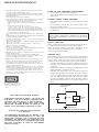
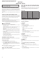
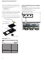
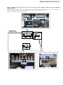
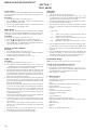
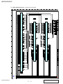
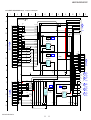
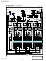
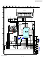
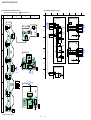
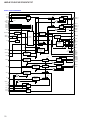
THIS NOTE IS COMMON FOR PRINTED WIRING BOARDS AND SCHEMATIC DIAGRAMS.
(In addition to this, the necessary note is printed in each block.)
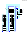
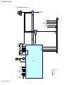
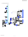
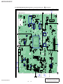
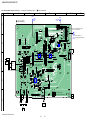
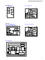
CONNECT board
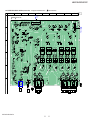
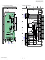
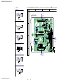
For Printed Wiring Boards.
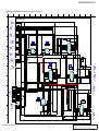
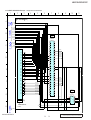
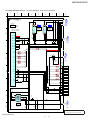
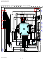
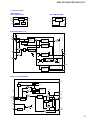
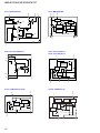
For Schematic Diagrams.
Note:
• X : Parts extracted from the component side.
• Y : Parts extracted from the conductor side.
•
f : Internal component.
•
: Pattern from the side which enables seeing.
(The other layers' patterns are not indicated.)
Note:
• All capacitors are in μF unless otherwise noted. (p: pF) 50
WV or less are not indicated except for electrolytics and
tantalums.
• All resistors are in Ω and 1/4 W or less unless otherwise
specified.
•
f : internal component.
• 2 : nonflammable resistor.
• 5 : fusible resistor.
• C : panel designation.
Caution:
Pattern face side:
(Conductor Side)
Parts face side:
(Component Side)
Parts on the pattern face side seen
from the pattern face are indicated.
Parts on the parts face side seen from
the parts face are indicated.
• MAIN and MB-134 boards are multi-layer printed board.
However, the patterns of intermediate-layers have not
been included in this diagrams.
• Indication of transistor.
C
Note:
The components identified by mark 0 or dotted
line with mark 0 are critical for safety.
Replace only with part
number specified.
Note 1: When the MAIN board is replaced, spread the compound referring to “NOTE OF REPLACING THE
IC3100, IC3200 AND IC3400 ON THE MAIN
BOARD AND THE COMPLETE MAIN BOARD”
on servicing notes (page 8).
Note 2: When the POWER board is replaced, spread the
compound referring to “NOTE OF REPLACING
THE D913, D931, IC901 AND IC921 ON THE
POWER BOARD AND THE COMPLETE POWER
BOARD” on servicing notes (page 9).
Note 1: When the MAIN board is replaced, spread the compound referring to “NOTE OF REPLACING THE
IC3100, IC3200 AND IC3400 ON THE MAIN
BOARD AND THE COMPLETE MAIN BOARD”
on servicing notes (page 8).
These are omitted.
B E
Q
B C
E
These are omitted.
• Abbreviation
CND : Canadian model
• Lead layouts
Lead layout of conventional IC
surface
CSP (Chip Size Package)
TUNER (FM) (TU1)
AUDIO board
R-USB board
P-KEY board
MAIN board
REG board
POWER board
KEY board
FL board
Note 2: When the POWER board is replaced, spread the
compound referring to “NOTE OF REPLACING
THE D913, D931, IC901 AND IC921 ON THE
POWER BOARD AND THE COMPLETE POWER
BOARD” on servicing notes (page 9).
HBD-E370/E470/E570/E870/T57
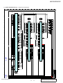
MB-134 board
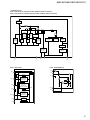
Note:
Les composants identifiés
par une marque 0 sont
critiques pour la sécurité.
Ne les remplacer que par
une piéce portant le numéro spécifié.
• A : B+ Line.
• B : B– Line.
• Voltages and waveforms are dc with respect to ground
under no-signal conditions.
– MB-134 board –
no mark : BD PLAY
* : Impossible to measure
– Other boards –
no mark : TUNER
* : Impossible to measure
• Voltages are taken with VOM (Input impedance 10 MΩ).
Voltage variations may be noted due to normal production
tolerances.
• Waveforms are taken with a oscilloscope.
Voltage variations may be noted due to normal production
tolerances.
• Circled numbers refer to waveforms.
• Signal path.
F
: AUDIO
E
: VIDEO
J
: DISC PLAY
L : USB
d
: LAN
f
: TUNER
N
: MIC
• Abbreviation
CND : Canadian model
• The voltage and waveform of CSP (chip size package)
cannot be measured, becaise its lead layout is different
from that of conventional IC.
Q
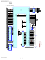
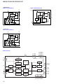
• Circuit Boards Location
34
34
F-USB board