1
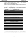
DRAGNOTT Quick start Guide
Created by Vitaliy Jungle
DRAGNOTT 2.2
1. Introduction.
DRAGNOTT tool (formerly known as PRCNM) enables you:
•
•
•
•
•
to change a CPU String Name of the AMD processor;
to enter the AMD K7 family processor the low power state;
to change an internal clock divisor of both Halt and Stop Grant low power states;
to change a clock frequency divisor of the mobile AMD K7 or AMD64 processor;
to configure the memory signal edge timings for a large number of system chipsets.
2. How it works.
DRAGNOTT doesn’t have any graphic user interface. It works without confirmations and notifications and
it is halted when its tasks are completed. Just create a shortcut to DRAGNOTT and place it into the Startup
folder or create a new value under the Run section in the System Registry – HKEY_LOCAL_MACHINE\
SOFTWARE\Microsoft\Windows\CurrentVersion\Run.
2.1. Modification of the CPU String Name.
The AMD Athlon XP, AMD Duron (680h) and AMD64 processors support processor string name
modification feature. To change the CPU String Name open PrcnmCfg.ini file and set a new string name
for the ProcessorName parameter. If you don’t want to modify the processor name just delete all the
characters after the ‘=’ sign.
2.2. Enabling and disabling of the low power state of the processor.
DRAGNOTT supports all of chipsets that are identified by Central Brain Identifier. But DRAGNOTT
doesn’t support an independent Stop Grant and Halt states control. To enter the processor a low state
DRAGNOTT enables both Halt state and Stop Grant state, and vice versa, to exit the processor a low
power state DRAGNOTT disables both Halt state and Stop Grant state. To enable a low power state just
open PrcnmCfg.ini file and set 1 to the LowPower parameter and for disabling set 0 for it. If you don’t
need to enable or disable a low power state for the processor just set 2 to the LowPower parameter.
2.3. Adjustment of internal clock divisors.
When the processor is in the low power state, Halt state or Stop Grant state, you can select an internal
clock divisor for every state for less theoretical power consumption. Open PrcnmCfg.ini configuration file
and set to the HALTDivisor and STPGNTDivisor parameters a new value. The valid divisors are 8, 16, 32,
64, 128, 256 and 512. Other values are ignorable by DRAGNOTT. Note that this option works with the
AMD processors having a CPUID of 63xh and higher and doesn’t applicable for the AMD64 processors
as 64-bit CPUs don’t have CLK_CTL Machine Specific Register.
2.4. FID transition of the mobile processor.
DRAGNOTT tool may increase or decrease a clock frequency of any AMD K7 or AMD64 processor
that implements the AMD PowerNow! or Cool’n Quiet Technology. To enable FID transition, open
PrcnmCfg.ini configuration file, locate the FIDTransition parameter and assign 1 to it. Below it there is
another parameter called ClkRatio that defines a clock frequency divisor of the mobile processor. You
must know the following valid clock ratio encodings:
AMD K7: 3 – x3.0, 4 – x4.0, 5 – x5.0, 55 – x5.5, 6 – x6.0, 65 – x6.5, 7 – x7.0, 75 – x7.5, 8 – x8.0, 85 –
x8.5, 9 – x9.0, 95 – x9.5, 10 – x10.0, 105 – x10.5, 11 – x11.0, 115 – x11.5, 12 – x12.0, 125 – x12.5, 13 –
x13.0, 135 – x13.5, 14 – x14.0, 15 – x15.0, 16 – x16.0, 165 – x16.5, 17 – x17.0, 18 – x18.0, 19 – x19.0,
20 – x20.0, 21 – x21.0, 22 – x22.0, 23 – x23.0, 24 – x24.0;
AMD64: 4 – x4.0, 5 – x5.0, 6 – x6.0, 7 – x7.0, 8 – x8.0, 9 – x9.0, 10 – x10.0, 11 – x11.0, 12 – x12.0,
13 – x13.0, 14 – x14.0, 15 – x15.0, 155 – x15.5, 16 – x16.0, 17 – x17.0, 175 – x17.5, 18 – x18.0, 19 –
x19.0, 20 – x20.0, 22 – x22.0, 225 – x22.5, 23 – x23.0, 24 – x24.0;
For example, to set a clock ratio to x12.5 you have to assign 1 to the FIDTransition parameter and
assign 125 to the ClkRatio parameter. To disable a FID transition just set 0 to the FIDTransition.
Page 1
DRAGNOTT Quick start Guide
Created by Vitaliy Jungle
Please note, DRAGNOTT doesn’t have a clock ratio range check. For example, if the mobile
processor has a maximum clock ratio of x11.0 and you are attempting to set a clock ratio of x12.0 then
DRAGNOTT will not inform you about the failed FID transition.
Additionally, before FID transition DRAGNOTT checks the presence of the mobile features of the AMD
processor. If the processor is not mobile DRAGNOTT doesn’t initiate FID transition preventing a “blue
screen of death” appearance.
2.5. Configuring of the memory signal edge timings.
Since version 2.0 DRAGNOTT supports a lot of popular chipsets both for AMD and Intel platforms in
order to change the most important DRAM timings. The following table shows what chipsets and
appropriate to them DRAM timings are supported by DRAGNOTT:
Chipset Name
VIA VP3
VIA MVP3
VIA MVP4 – VT8501
VIA ProMedia – VT8601
VIA PLE133 – VT8601A
VIA KLE133 – VT8361
VIA KX133 – VT8371
VIA KT133 – VT8363
VIA KT133A – VT8363A
VIA KT266 – VT8366
VIA KT266A – VT8366A
VIA KM266
VIA KT333 – VT8367
VIA KT400 – VT8368
VIA KT400A – VT8368A
VIA KT600
SiS600
SiS620
SiS630
SiS735
SiS741GX
SiS746
SiS748
AMD761
AMD762
nVidia nForce Series
nVidia nForce2 Series
Intel 440BX/ZX
Intel 810/E/E2
Intel 815/E/EP
Intel 845G/GL/GV
Intel 848P
Intel 852GME
Intel 852PM
Intel 854
Intel 865G/GV
Intel 865P/PE
Intel 875P
Applicable DRAM Timings
tCL, tRAS, tRCD, tRP
tCL, tRAS, tRCD, tRP
tCL, tRAS, tRCD, tRP
tCL, tRAS, tRCD, tRP
tCL, tRAS, tRCD, tRP, VIABL*
tCL, tRAS, tRCD, tRP, VIABL
tCL, tRAS, tRCD, tRP, VIABL
tCL, tRAS, tRCD, tRP, VIABL
tCL, tRAS, tRCD, tRP, VIABL
tCL, tRAS, tRCD, tRP, tWR, tWTR, VIABL
tCL, tRAS, tRCD, tRP, tWR, tWTR, VIABL
tCL, tRAS, tRCD, tRP, tWR, tWTR, VIABL
tCL, tRAS, tRCD, tRP, tWR, tWTR, VIABL
tCL, tRAS, tRCD, tRP, tWR, tWTR, VIABL
tCL, tRAS, tRCD, tRP, tWR, tWTR, VIABL
tCL, tRAS, tRCD, tRP, tWR, tWTR, VIABL
tCL, tRAS, tRCD, tRP
tCL, tRAS, tRCD, tRP
tCL, tRAS, tRCD, tRP, tWR, tRRD
tCL, tRAS, tRCD, tRP, tWR
tCL, tRAS, tRCD, tRP, tWR, tWTR
tCL, tRAS, tRCD, tRP, tWR, tWTR
tCL, tRAS, tRCD, tRP, tRC, tWR, tWTR
tCL, tRAS, tRCD, tRP, tRC, tWR, tWTR
tCL, tRAS, tRCD, tRP, tRC, tWR, tWTR
tCL, tRAS, tRCDR, tRCDW, tRP, tRC, tRFC, tWTR, tRTW
tCL, tRAS, tRCDR, tRCDW, tRP, tRC, tRFC, tWTR, tRTW
tCL, tRCD, tRP
tCL, tRAS, tRCD, tRP
tCL, tRAS, tRCD, tRP, tRC
tCL, tRAS, tRCD, tRP
tCL, tRAS, tRCD, tRP
tCL, tRAS, tRCD, tRP, tRFC, tWR
tCL, tRAS, tRCD, tRP, tRFC, tWR
tCL, tRAS, tRCD, tRP, tRFC, tWR
tCL, tRAS, tRCD, tRP
tCL, tRAS, tRCD, tRP
tCL, tRAS, tRCD, tRP
*VIABL – bank interleave
So, to configure a desired memory signal edge timing make sure your chipset is in the table above.
Then open PrcnmCfg.ini configuration file, locate the DRAMTimings parameter and set 1 to it. Using the
table above, in the configuration file locate appropriate parameters having the same names as applicable
DRAM timings and assigned a valid DRAM timing value to them.
Page 2
DRAGNOTT Quick start Guide
Created by Vitaliy Jungle
2.5.1. Configuring of the DRAM timing parameters for the appropriate chipsets.
• VIA VP3, VIA MVP3, VIA MVP4 Chipsets.
tCL: 1, 2, 3; tRAS: 5, 6; tRCD: 2, 3; tRP: 2, 3; VIABL: 0, 2, 4.
• VIA ProMedia, VIA PLE133, VIA KT133/A, VIA KX133, VIA KLE133 Chipsets.
tCL: 1, 2, 3; tRAS: 5, 6; tRCD: 2, 3; tRP: 2, 3; VIABL: 0, 2, 4.
• VIA KM266, VIA KT266/A, VIA KT333 Chipsets.
tCL: 2, 25, 3; tRAS: 5, 6; tRCD: 2, 3; tRP: 2, 3; tWR: 1, 2; tWTR: 1, 2; VIAIL: 0, 2, 4.
• VIA KT400/A Chipsets.
tCL: 15, 2, 25, 3; tRAS: 6, 7; tRCD: 2, 3; tRP: 2, 3; tWR: 2, 3; tWTR: 1, 3; VIAIL: 0, 2, 4.
• VIA KT600 Chipset.
tCL: 15, 2, 25, 3; tRAS: 6, 7, 8, 9; tRCD: 2, 3, 4, 5; tRP: 2, 3, 4, 5; tWR: 2, 3; tWTR: 1, 2;
VIAIL: 0, 2, 4.
• SiS600, SiS620 Chipsets.
tCL: 2, 3; tRAS: 4, 5, 6, 7; tRCD: 2, 3, 4, 5; tRP: 2, 3, 4, 5.
• SiS630 Chipset.
tCL: 2, 3; tRAS: 4, 5, 6, 7; tRCD: 2, 3, 4, 5; tRP: 2, 3, 4, 5; tWR: 1, 2; tRRD: 1, 2.
• SiS735 Chipset.
tCL: 2, 3; tRAS: 4, 5, 6, 7; tRCD: 2, 3, 4; tRP: 2, 3, 4; tWR: 1, 2.
• SiS741, SiS746, SiS748 Chipsets.
tCL: 2, 25, 3; tRAS: 4, 5, 6, 7, 8, 9, 10, 11; tRCD: 2, 3, 4, 5; tRP: 2, 3, 4, 5; tWR: 1, 2, 3; tWTR: 1, 2.
• AMD761, AMD762 Chipsets.
tCL: 2, 25, 3; tRAS: 2, 3, 4, 5, 6, 7, 8, 9; tRCD: 1, 2, 3, 4; tRP: 3, 4; tRC: 3, 4, 5, 6, 7, 8, 9, 10;
tWR: 1, 2, 3; tWTR: 1, 2.
• NVidia nForce, NVidia nForce2 Series Chipsets.
tCL: 2, 25, 3; tRAS: 5, 6, 7, 8, 9, 10, 11, 12, 13, 14, 15; tRP: 2, 3, 4, 5, 6;
tRC: 7, 8, 9, 10, 11, 12, 13, 14, 15, 16, 17, 18, 19, 20, 21, 22, 23, 24;
tRFC: 8, 9, 10, 11, 12, 13, 14, 15, 16, 17, 18, 19, 20, 21, 22, 23, 24;
tRCDR: 2, 3, 4, 5, 6; tRCDW: 2, 3, 4, 5, 6; tWTR: 1, 2, 3, 4, 5, 6; tRTW: 1, 2, 3, 4, 5, 6.
• Intel 440BX/ZX Chipsets.
tCL: 2, 3; tRCD: 2, 3; tRP: 2, 3.
• Intel 810/E/E2 Chipsets.
tCL: 2, 3; tRAS: 5, 6; tRCD: 2, 3; tRP: 2, 3.
• Intel 815/E/EP Chipsets.
tCL: 2, 3; tRAS: 5, 7; tRCD: 2, 3; tRP: 2, 3; tRC: 7, 9.
• Intel 845G/GL/GV Chipsets.
tCL: 2, 25; tRAS: 5, 6, 7, 8; tRCD: 2, 3; tRP: 2, 3.
• Intel 848P Chipset.
tCL: 2, 25, 3; tRAS: 5, 6, 7, 8, 9, 10; tRCD: 2, 3, 4; tRP: 2, 3, 4.
• Intel 852GME/852PM Chipsets.
tCL: 2, 25. tRAS: 5, 6, 7, 8; tRCD: 2, 3, 4; tRP: 2, 3, 4; tRFC: 7, 8, 9, 10, 11, 12, 13, 14; tWTR: 2, 3.
• Intel 854 Chipset.
tCL: 2, 25. tRAS: 5, 6, 7, 8; tRCD: 2, 3, 4; tRP: 2, 3, 4; tRFC: 7, 8, 9, 10, 11, 12, 13, 14; tWTR: 2, 3.
• Intel 865G/GV Chipsets.
tCL: 2, 25, 3; tRAS: 5, 6, 7, 8, 9, 10; tRCD: 2, 3, 4; tRP: 2, 3, 4.
• Intel 865P/PE Chipsets.
tCL: 2, 25, 3; tRAS: 5, 6, 7, 8, 9, 10; tRCD: 2, 3, 4; tRP: 2, 3, 4.
• Intel 875P Chipset.
tCL: 2, 25, 3; tRAS: 5, 6, 7, 8, 9, 10; tRCD: 2, 3, 4; tRP: 2, 3, 4.
Example 1. We intend to change only one tCAS DRAM timing of the nVidia nForce2 chipset to 2.5T. So,
open PrcnmCfg.ini file, set 1 to the DRAMTimings parameter, set 25 to the tCAS parameter. Besides,
make sure the other timing parameters of the PrcnmCfg.ini configuration file don’t have any values. Save
settings. No need to set all the timings, just select the desired.
Note, DRAGNOTT works with only timings that are properly defined for every chipset from the table
above. For example, if you mistakenly set a value to the tWTR parameter for the VIA KT133 chipset
DRAGNOTT will ignore this user mistake.
Page 3