1
XST User Guide
10.1
R
R
Xilinx is disclosing this user guide, manual, release note, and/or specification (the "Documentation") to you solely for use in the development
of designs to operate with Xilinx hardware devices. You may not reproduce, distribute, republish, download, display, post, or transmit the
Documentation in any form or by any means including, but not limited to, electronic, mechanical, photocopying, recording, or otherwise,
without the prior written consent of Xilinx. Xilinx expressly disclaims any liability arising out of your use of the Documentation. Xilinx reserves
the right, at its sole discretion, to change the Documentation without notice at any time. Xilinx assumes no obligation to correct any errors
contained in the Documentation, or to advise you of any corrections or updates. Xilinx expressly disclaims any liability in connection with
technical support or assistance that may be provided to you in connection with the Information.
THE DOCUMENTATION IS DISCLOSED TO YOU “AS-IS” WITH NO WARRANTY OF ANY KIND. XILINX MAKES NO OTHER
WARRANTIES, WHETHER EXPRESS, IMPLIED, OR STATUTORY, REGARDING THE DOCUMENTATION, INCLUDING ANY
WARRANTIES OF MERCHANTABILITY, FITNESS FOR A PARTICULAR PURPOSE, OR NONINFRINGEMENT OF THIRD-PARTY
RIGHTS. IN NO EVENT WILL XILINX BE LIABLE FOR ANY CONSEQUENTIAL, INDIRECT, EXEMPLARY, SPECIAL, OR INCIDENTAL
DAMAGES, INCLUDING ANY LOSS OF DATA OR LOST PROFITS, ARISING FROM YOUR USE OF THE DOCUMENTATION.
© 2002–2008 Xilinx, Inc. All rights reserved.
XILINX, the Xilinx logo, the Brand Window, and other designated brands included herein are trademarks of Xilinx, Inc. All other trademarks
are the property of their respective owners
XST User Guide
www.xilinx.com
10.1
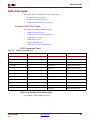
Table of Contents
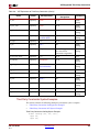
Preface: About the XST User Guide
XST User Guide Contents . . . . . . . . . . . . . . . . . . . . . . . . . . . . . . . . . . . . . . . . . . . . . . . . . . . 27
Additional Resources . . . . . . . . . . . . . . . . . . . . . . . . . . . . . . . . . . . . . . . . . . . . . . . . . . . . . . . 28
Conventions . . . . . . . . . . . . . . . . . . . . . . . . . . . . . . . . . . . . . . . . . . . . . . . . . . . . . . . . . . . . . . . . 28
Typographical . . . . . . . . . . . . . . . . . . . . . . . . . . . . . . . . . . . . . . . . . . . . . . . . . . . . . . . . . . . . 28
Online Document . . . . . . . . . . . . . . . . . . . . . . . . . . . . . . . . . . . . . . . . . . . . . . . . . . . . . . . . . 29
Chapter 1: Introduction to the XST User Guide
About XST . . . . . . . . . . . . . . . . . . . . . . . . . . . . . . . . . . . . . . . . . . . . . . . . . . . . . . . . . . . . . . . . . . 31
What’s New in Release 10.1. . . . . . . . . . . . . . . . . . . . . . . . . . . . . . . . . . . . . . . . . . . . . . . . . . 31
Macro Inference . . . . . . . . . . . . . . . . . . . . . . . . . . . . . . . . . . . . . . . . . . . . . . . . . . . . . . . . . . 31
Constraints . . . . . . . . . . . . . . . . . . . . . . . . . . . . . . . . . . . . . . . . . . . . . . . . . . . . . . . . . . . . . . 31
Libraries Support . . . . . . . . . . . . . . . . . . . . . . . . . . . . . . . . . . . . . . . . . . . . . . . . . . . . . . . . . 32
Setting XST Options . . . . . . . . . . . . . . . . . . . . . . . . . . . . . . . . . . . . . . . . . . . . . . . . . . . . . . . . 32
Chapter 2: XST HDL Coding Techniques
Signed and Unsigned Support in XST . . . . . . . . . . . . . . . . . . . . . . . . . . . . . . . . . . . . . . . 34
Registers HDL Coding Techniques . . . . . . . . . . . . . . . . . . . . . . . . . . . . . . . . . . . . . . . . . . 35
About Registers . . . . . . . . . . . . . . . . . . . . . . . . . . . . . . . . . . . . . . . . . . . . . . . . . . . . . . . . . .
Registers Log File . . . . . . . . . . . . . . . . . . . . . . . . . . . . . . . . . . . . . . . . . . . . . . . . . . . . . . . . .
Registers Related Constraints. . . . . . . . . . . . . . . . . . . . . . . . . . . . . . . . . . . . . . . . . . . . . . .
Registers Coding Examples . . . . . . . . . . . . . . . . . . . . . . . . . . . . . . . . . . . . . . . . . . . . . . . .
Flip-Flop With Positive-Edge Clock . . . . . . . . . . . . . . . . . . . . . . . . . . . . . . . . . . . . . . . .
Flip-Flop With Negative-Edge Clock and Asynchronous Reset . . . . . . . . . . . . . . . . . . .
Flip-Flop With Positive-Edge Clock and Synchronous Set . . . . . . . . . . . . . . . . . . . . . . .
Flip-Flop With Positive-Edge Clock and Clock Enable . . . . . . . . . . . . . . . . . . . . . . . . . .
4-Bit Register With Positive-Edge Clock, Asynchronous Set, and Clock Enable. . . . . . .
35
35
36
36
36
38
39
41
42
Latches HDL Coding Techniques . . . . . . . . . . . . . . . . . . . . . . . . . . . . . . . . . . . . . . . . . . . . 44
About Latches . . . . . . . . . . . . . . . . . . . . . . . . . . . . . . . . . . . . . . . . . . . . . . . . . . . . . . . . . . . .
Latches Log File . . . . . . . . . . . . . . . . . . . . . . . . . . . . . . . . . . . . . . . . . . . . . . . . . . . . . . . . . .
Latches Related Constraints . . . . . . . . . . . . . . . . . . . . . . . . . . . . . . . . . . . . . . . . . . . . . . . .
Latches Coding Examples . . . . . . . . . . . . . . . . . . . . . . . . . . . . . . . . . . . . . . . . . . . . . . . . . .
Latch With Positive Gate . . . . . . . . . . . . . . . . . . . . . . . . . . . . . . . . . . . . . . . . . . . . . . . .
Latch With Positive Gate and Asynchronous Reset . . . . . . . . . . . . . . . . . . . . . . . . . . . .
4-Bit Latch With Inverted Gate and Asynchronous Set . . . . . . . . . . . . . . . . . . . . . . . . .
44
44
44
45
45
46
48
Tristates HDL Coding Techniques . . . . . . . . . . . . . . . . . . . . . . . . . . . . . . . . . . . . . . . . . . . 49
About Tristates . . . . . . . . . . . . . . . . . . . . . . . . . . . . . . . . . . . . . . . . . . . . . . . . . . . . . . . . . . .
Tristates Log File . . . . . . . . . . . . . . . . . . . . . . . . . . . . . . . . . . . . . . . . . . . . . . . . . . . . . . . . .
Tristates Related Constraints . . . . . . . . . . . . . . . . . . . . . . . . . . . . . . . . . . . . . . . . . . . . . . .
Tristates Coding Examples . . . . . . . . . . . . . . . . . . . . . . . . . . . . . . . . . . . . . . . . . . . . . . . . .
Tristate Description Using Combinatorial Process and Always Block . . . . . . . . . . . . . .
Tristate Description Using Concurrent Assignment . . . . . . . . . . . . . . . . . . . . . . . . . . . .
49
49
50
50
50
52
Counters HDL Coding Techniques . . . . . . . . . . . . . . . . . . . . . . . . . . . . . . . . . . . . . . . . . . 53
About Counters . . . . . . . . . . . . . . . . . . . . . . . . . . . . . . . . . . . . . . . . . . . . . . . . . . . . . . . . . . 53
XST User Guide
10.1
www.xilinx.com
3
R
Counters Log File . . . . . . . . . . . . . . . . . . . . . . . . . . . . . . . . . . . . . . . . . . . . . . . . . . . . . . . . .
Counters Related Constraints . . . . . . . . . . . . . . . . . . . . . . . . . . . . . . . . . . . . . . . . . . . . . .
Counters Coding Examples . . . . . . . . . . . . . . . . . . . . . . . . . . . . . . . . . . . . . . . . . . . . . . . .
4-Bit Unsigned Up Counter With Asynchronous Reset . . . . . . . . . . . . . . . . . . . . . . . . .
4-Bit Unsigned Down Counter With Synchronous Set . . . . . . . . . . . . . . . . . . . . . . . . . .
4-Bit Unsigned Up Counter With Synchronous Load With Constant . . . . . . . . . . . . . . .
4-Bit Unsigned Up Counter With Asynchronous Reset and Clock Enable . . . . . . . . . . .
4-Bit Unsigned Up/Down Counter With Asynchronous Reset . . . . . . . . . . . . . . . . . . .
4-Bit Signed Up Counter With Asynchronous Reset. . . . . . . . . . . . . . . . . . . . . . . . . . . .
4-Bit Signed Up Counter With Asynchronous Reset and Modulo Maximum . . . . . . . .
53
54
54
54
56
59
62
64
66
68
Accumulators HDL Coding Techniques . . . . . . . . . . . . . . . . . . . . . . . . . . . . . . . . . . . . . 70
About Accumulators . . . . . . . . . . . . . . . . . . . . . . . . . . . . . . . . . . . . . . . . . . . . . . . . . . . . . .
Accumulators in Virtex-4 and Virtex-5 Devices . . . . . . . . . . . . . . . . . . . . . . . . . . . . . . .
Accumulators Log File . . . . . . . . . . . . . . . . . . . . . . . . . . . . . . . . . . . . . . . . . . . . . . . . . . . .
Accumulators Related Constraints . . . . . . . . . . . . . . . . . . . . . . . . . . . . . . . . . . . . . . . . . .
Accumulators Coding Examples . . . . . . . . . . . . . . . . . . . . . . . . . . . . . . . . . . . . . . . . . . . .
4-Bit Unsigned Up Accumulator With Asynchronous Reset . . . . . . . . . . . . . . . . . . . . .
70
70
71
71
71
72
Shift Registers HDL Coding Techniques . . . . . . . . . . . . . . . . . . . . . . . . . . . . . . . . . . . . 74
About Shift Registers . . . . . . . . . . . . . . . . . . . . . . . . . . . . . . . . . . . . . . . . . . . . . . . . . . . . . .
Describing Shift Registers . . . . . . . . . . . . . . . . . . . . . . . . . . . . . . . . . . . . . . . . . . . . . . . . . .
Implementing Shift Registers . . . . . . . . . . . . . . . . . . . . . . . . . . . . . . . . . . . . . . . . . . . . . . .
Hardware Resources to Implement Shift Registers . . . . . . . . . . . . . . . . . . . . . . . . . . . . .
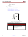
SRL16 and SRLC16 . . . . . . . . . . . . . . . . . . . . . . . . . . . . . . . . . . . . . . . . . . . . . . . . . . . . .
SRL16 and SRLC16 Pin Layout Diagrams. . . . . . . . . . . . . . . . . . . . . . . . . . . . . . . . . . . .
Shift Registers Log File . . . . . . . . . . . . . . . . . . . . . . . . . . . . . . . . . . . . . . . . . . . . . . . . . . . .
Shift Registers Related Constraints . . . . . . . . . . . . . . . . . . . . . . . . . . . . . . . . . . . . . . . . . .
Shift Registers Coding Examples . . . . . . . . . . . . . . . . . . . . . . . . . . . . . . . . . . . . . . . . . . . .
8-Bit Shift-Left Register With Positive-Edge Clock, Serial In and Serial Out . . . . . . . . .
8-Bit Shift-Left Register With Negative-Edge Clock, Clock Enable,
Serial In and Serial Out . . . . . . . . . . . . . . . . . . . . . . . . . . . . . . . . . . . . . . . . . . . . . . . .
8-Bit Shift-Left Register With Positive-Edge Clock,
Asynchronous Reset, Serial In and Serial Out . . . . . . . . . . . . . . . . . . . . . . . . . . . . . .
8-Bit Shift-Left Register With Positive-Edge Clock, Synchronous Set,
Serial In and Serial Out . . . . . . . . . . . . . . . . . . . . . . . . . . . . . . . . . . . . . . . . . . . . . . . .
8-Bit Shift-Left Register With Positive-Edge Clock,
Serial In and Parallel Out . . . . . . . . . . . . . . . . . . . . . . . . . . . . . . . . . . . . . . . . . . . . . .
8-Bit Shift-Left Register With Positive-Edge Clock,
Asynchronous Parallel Load, Serial In and Serial Out . . . . . . . . . . . . . . . . . . . . . . . .
8-Bit Shift-Left Register With Positive-Edge Clock,
Synchronous Parallel Load, Serial In and Serial Out . . . . . . . . . . . . . . . . . . . . . . . . .
8-Bit Shift-Left/Shift-Right Register With Positive-Edge Clock,
Serial In and Parallel Out . . . . . . . . . . . . . . . . . . . . . . . . . . . . . . . . . . . . . . . . . . . . . .
74
74
75
75
75
76
76
77
77
78
79
82
84
86
87
89
91
Dynamic Shift Registers HDL Coding Techniques . . . . . . . . . . . . . . . . . . . . . . . . . . . 93
About Dynamic Shift Registers . . . . . . . . . . . . . . . . . . . . . . . . . . . . . . . . . . . . . . . . . . . . .
Dynamic Shift Registers Log File . . . . . . . . . . . . . . . . . . . . . . . . . . . . . . . . . . . . . . . . . . . .
Dynamic Shift Registers Related Constraints . . . . . . . . . . . . . . . . . . . . . . . . . . . . . . . . .
Dynamic Shift Registers Coding Examples . . . . . . . . . . . . . . . . . . . . . . . . . . . . . . . . . . .
93
94
94
94
16-Bit Dynamic Shift Register With Positive-Edge Clock,
Serial In and Serial Out . . . . . . . . . . . . . . . . . . . . . . . . . . . . . . . . . . . . . . . . . . . . . . . . 95
Multiplexers HDL Coding Techniques . . . . . . . . . . . . . . . . . . . . . . . . . . . . . . . . . . . . . . 97
About Multiplexers . . . . . . . . . . . . . . . . . . . . . . . . . . . . . . . . . . . . . . . . . . . . . . . . . . . . . . . 97
Multiplexers Case Statements . . . . . . . . . . . . . . . . . . . . . . . . . . . . . . . . . . . . . . . . . . . . . . 98
Multiplexers Case Statement Examples . . . . . . . . . . . . . . . . . . . . . . . . . . . . . . . . . . . . . 98
4
www.xilinx.com
XST User Guide
10.1
R
Verilog Case Implementation Style Parameter . . . . . . . . . . . . . . . . . . . . . . . . . . . . . . . . 99
Verilog Case Statement Resources . . . . . . . . . . . . . . . . . . . . . . . . . . . . . . . . . . . . . . . . . 99
Multiplexers Log File . . . . . . . . . . . . . . . . . . . . . . . . . . . . . . . . . . . . . . . . . . . . . . . . . . . . .
Multiplexers Related Constraints . . . . . . . . . . . . . . . . . . . . . . . . . . . . . . . . . . . . . . . . . .
Multiplexers Coding Examples . . . . . . . . . . . . . . . . . . . . . . . . . . . . . . . . . . . . . . . . . . . .
4-to-1 1-Bit MUX Using IF Statement . . . . . . . . . . . . . . . . . . . . . . . . . . . . . . . . . . . . . .
4-to-1 1-Bit MUX Using Case Statement . . . . . . . . . . . . . . . . . . . . . . . . . . . . . . . . . . . .
4-to-1 1-Bit MUX Using Tristate Buffers . . . . . . . . . . . . . . . . . . . . . . . . . . . . . . . . . . . .
No 4-to-1 MUX (3-to-1 1-Bit MUX With 1-Bit Latch) . . . . . . . . . . . . . . . . . . . . . . . . . .
100
100
100
100
102
104
105
Decoders HDL Coding Techniques . . . . . . . . . . . . . . . . . . . . . . . . . . . . . . . . . . . . . . . . . 107
About Decoders . . . . . . . . . . . . . . . . . . . . . . . . . . . . . . . . . . . . . . . . . . . . . . . . . . . . . . . . .
Decoders Log File . . . . . . . . . . . . . . . . . . . . . . . . . . . . . . . . . . . . . . . . . . . . . . . . . . . . . . . .
Decoders Related Constraints . . . . . . . . . . . . . . . . . . . . . . . . . . . . . . . . . . . . . . . . . . . . .
Decoders Coding Examples . . . . . . . . . . . . . . . . . . . . . . . . . . . . . . . . . . . . . . . . . . . . . . .
1-of-8 Decoder (One-Hot) . . . . . . . . . . . . . . . . . . . . . . . . . . . . . . . . . . . . . . . . . . . . . . .
1-of-8 Decoder (One-Cold) . . . . . . . . . . . . . . . . . . . . . . . . . . . . . . . . . . . . . . . . . . . . . .
Decoder With Unselected Outputs . . . . . . . . . . . . . . . . . . . . . . . . . . . . . . . . . . . . . . . .
107
107
108
108
108
109
111
Priority Encoders HDL Coding Techniques . . . . . . . . . . . . . . . . . . . . . . . . . . . . . . . . . 113
About Priority Encoders . . . . . . . . . . . . . . . . . . . . . . . . . . . . . . . . . . . . . . . . . . . . . . . . . .
Priority Encoders Log File . . . . . . . . . . . . . . . . . . . . . . . . . . . . . . . . . . . . . . . . . . . . . . . .
Priority Encoders Related Constraints . . . . . . . . . . . . . . . . . . . . . . . . . . . . . . . . . . . . . .
Priority Encoders Coding Examples . . . . . . . . . . . . . . . . . . . . . . . . . . . . . . . . . . . . . . . .
3-Bit 1-of-9 Priority Encoder . . . . . . . . . . . . . . . . . . . . . . . . . . . . . . . . . . . . . . . . . . . . .
113
113
114
114
114
Logical Shifters HDL Coding Techniques . . . . . . . . . . . . . . . . . . . . . . . . . . . . . . . . . . 115
About Logical Shifters . . . . . . . . . . . . . . . . . . . . . . . . . . . . . . . . . . . . . . . . . . . . . . . . . . . .
Logical Shifters Log File . . . . . . . . . . . . . . . . . . . . . . . . . . . . . . . . . . . . . . . . . . . . . . . . . .
Logical Shifters Related Constraints . . . . . . . . . . . . . . . . . . . . . . . . . . . . . . . . . . . . . . . .
Logical Shifters Coding Examples . . . . . . . . . . . . . . . . . . . . . . . . . . . . . . . . . . . . . . . . . .
Logical Shifter One . . . . . . . . . . . . . . . . . . . . . . . . . . . . . . . . . . . . . . . . . . . . . . . . . . . .
Logical Shifter Three . . . . . . . . . . . . . . . . . . . . . . . . . . . . . . . . . . . . . . . . . . . . . . . . . . .
115
116
116
116
117
119
Arithmetic Operators HDL Coding Techniques . . . . . . . . . . . . . . . . . . . . . . . . . . . . . 121
About Arithmetic Operators . . . . . . . . . . . . . . . . . . . . . . . . . . . . . . . . . . . . . . . . . . . . . .
Arithmetic Operators Log File . . . . . . . . . . . . . . . . . . . . . . . . . . . . . . . . . . . . . . . . . . . . .
Arithmetic Operators Related Constraints . . . . . . . . . . . . . . . . . . . . . . . . . . . . . . . . . . .
Arithmetic Operators Coding Examples . . . . . . . . . . . . . . . . . . . . . . . . . . . . . . . . . . . .
121
121
122
122
Adders, Subtractors, and Adders/Subtractors HDL Coding Techniques . . . . . 122
About Adders, Subtractors, and Adders/Subtractors . . . . . . . . . . . . . . . . . . . . . . . . .
Adders, Subtractors, and Adders/Subtractors Log File . . . . . . . . . . . . . . . . . . . . . . .
Adders, Subtractors, and Adders/Subtractors Related Constraints . . . . . . . . . . . . .
Adders, Subtractors, and Adders/Subtractors Coding Examples . . . . . . . . . . . . . . .
Unsigned 8-Bit Adder . . . . . . . . . . . . . . . . . . . . . . . . . . . . . . . . . . . . . . . . . . . . . . . . . .
Unsigned 8-Bit Adder With Carry In . . . . . . . . . . . . . . . . . . . . . . . . . . . . . . . . . . . . . .
Unsigned 8-Bit Adder With Carry Out . . . . . . . . . . . . . . . . . . . . . . . . . . . . . . . . . . . . .
Unsigned 8-Bit Adder With Carry In and Carry Out . . . . . . . . . . . . . . . . . . . . . . . . . .
Signed 8-Bit Adder . . . . . . . . . . . . . . . . . . . . . . . . . . . . . . . . . . . . . . . . . . . . . . . . . . . .
Unsigned 8-Bit Subtractor . . . . . . . . . . . . . . . . . . . . . . . . . . . . . . . . . . . . . . . . . . . . . . .
Unsigned 8-Bit Subtractor With Borrow In . . . . . . . . . . . . . . . . . . . . . . . . . . . . . . . . . .
Unsigned 8-Bit Adder/Subtractor . . . . . . . . . . . . . . . . . . . . . . . . . . . . . . . . . . . . . . . .
122
123
123
123
124
125
126
129
130
132
133
134
Comparators HDL Coding Techniques . . . . . . . . . . . . . . . . . . . . . . . . . . . . . . . . . . . . . 135
About Comparators . . . . . . . . . . . . . . . . . . . . . . . . . . . . . . . . . . . . . . . . . . . . . . . . . . . . . . 135
Comparators Log File . . . . . . . . . . . . . . . . . . . . . . . . . . . . . . . . . . . . . . . . . . . . . . . . . . . . 135
Comparators Related Constraints . . . . . . . . . . . . . . . . . . . . . . . . . . . . . . . . . . . . . . . . . . 136
XST User Guide
10.1
www.xilinx.com
5
R
Comparators Coding Examples . . . . . . . . . . . . . . . . . . . . . . . . . . . . . . . . . . . . . . . . . . . . 136
Unsigned 8-Bit Greater or Equal Comparator . . . . . . . . . . . . . . . . . . . . . . . . . . . . . . . . 136
Multipliers HDL Coding Techniques . . . . . . . . . . . . . . . . . . . . . . . . . . . . . . . . . . . . . . . 137
About Multipliers . . . . . . . . . . . . . . . . . . . . . . . . . . . . . . . . . . . . . . . . . . . . . . . . . . . . . . . .
Large Multipliers Using Block Multipliers . . . . . . . . . . . . . . . . . . . . . . . . . . . . . . . . . . .
Registered Multipliers . . . . . . . . . . . . . . . . . . . . . . . . . . . . . . . . . . . . . . . . . . . . . . . . . . . .
Multipliers (Virtex-4, Virtex-5, and Spartan-3A D Devices) . . . . . . . . . . . . . . . . . . . .
Multiplication with Constant . . . . . . . . . . . . . . . . . . . . . . . . . . . . . . . . . . . . . . . . . . . . . .
Multipliers Log File . . . . . . . . . . . . . . . . . . . . . . . . . . . . . . . . . . . . . . . . . . . . . . . . . . . . . .
Multipliers Related Constraints . . . . . . . . . . . . . . . . . . . . . . . . . . . . . . . . . . . . . . . . . . . .
Multipliers Coding Examples . . . . . . . . . . . . . . . . . . . . . . . . . . . . . . . . . . . . . . . . . . . . .
Unsigned 8x4-Bit Multiplier . . . . . . . . . . . . . . . . . . . . . . . . . . . . . . . . . . . . . . . . . . . . .
138
138
138
138
139
139
140
140
140
Sequential Complex Multipliers HDL Coding Techniques . . . . . . . . . . . . . . . . . . 141
About Sequential Complex Multipliers . . . . . . . . . . . . . . . . . . . . . . . . . . . . . . . . . . . . .
Sequential Complex Multipliers Log File . . . . . . . . . . . . . . . . . . . . . . . . . . . . . . . . . . . .
Sequential Complex Multipliers Related Constraints . . . . . . . . . . . . . . . . . . . . . . . . .
Sequential Complex Multipliers Coding Examples . . . . . . . . . . . . . . . . . . . . . . . . . . .
Signed 18x18-bit Sequential Complex Multiplier . . . . . . . . . . . . . . . . . . . . . . . . . . . . .
141
142
142
142
142
Pipelined Multipliers HDL Coding Techniques . . . . . . . . . . . . . . . . . . . . . . . . . . . . 145
About Pipelined Multipliers . . . . . . . . . . . . . . . . . . . . . . . . . . . . . . . . . . . . . . . . . . . . . . .
Pipelined Multipliers Log File . . . . . . . . . . . . . . . . . . . . . . . . . . . . . . . . . . . . . . . . . . . . .
Pipelined Multipliers Related Constraints . . . . . . . . . . . . . . . . . . . . . . . . . . . . . . . . . . .
Pipelined Multipliers Coding Examples . . . . . . . . . . . . . . . . . . . . . . . . . . . . . . . . . . . .
Pipelined Multiplier (Outside, Single) . . . . . . . . . . . . . . . . . . . . . . . . . . . . . . . . . . . . .
Pipelined Multiplier (Inside, Single) . . . . . . . . . . . . . . . . . . . . . . . . . . . . . . . . . . . . . . .
Pipelined Multiplier (Outside, Shift). . . . . . . . . . . . . . . . . . . . . . . . . . . . . . . . . . . . . . .
145
146
146
147
147
149
151
Multiply Adder/Subtractors HDL Coding Techniques . . . . . . . . . . . . . . . . . . . . . . 153
About Multiply Adder/Subtractors . . . . . . . . . . . . . . . . . . . . . . . . . . . . . . . . . . . . . . . .
Multiply Adder/Subtractors in Virtex-4 and Virtex- 5 Devices . . . . . . . . . . . . . . . . .
Multiply Adder/Subtractors Log File. . . . . . . . . . . . . . . . . . . . . . . . . . . . . . . . . . . . . . .
Multiply Adder/Subtractors Related Constraints . . . . . . . . . . . . . . . . . . . . . . . . . . . .
Multiply Adder/Subtractors Coding Examples . . . . . . . . . . . . . . . . . . . . . . . . . . . . . .
Multiplier Adder With 2 Register Levels on Multiplier Inputs . . . . . . . . . . . . . . . . . . .
Multiplier Adder/Subtractor With 2 Register Levels On Multiplier Inputs . . . . . . . . .
153
153
154
154
155
155
157
Multiply Accumulate HDL Coding Techniques . . . . . . . . . . . . . . . . . . . . . . . . . . . . . 159
About Multiply Accumulate . . . . . . . . . . . . . . . . . . . . . . . . . . . . . . . . . . . . . . . . . . . . . .
Multiply Accumulate in Virtex-4 and Virtex-5 Devices . . . . . . . . . . . . . . . . . . . . . . . .
Multiply Accumulate Log File . . . . . . . . . . . . . . . . . . . . . . . . . . . . . . . . . . . . . . . . . . . . .
Multiply Accumulate Related Constraints . . . . . . . . . . . . . . . . . . . . . . . . . . . . . . . . . . .
Multiply Accumulate Coding Examples . . . . . . . . . . . . . . . . . . . . . . . . . . . . . . . . . . . .
Multiplier Up Accumulate With Register After Multiplication . . . . . . . . . . . . . . . . . .
Multiplier Up/Down Accumulate With Register After Multiplication . . . . . . . . . . . .
159
159
160
160
160
161
163
Dividers HDL Coding Techniques . . . . . . . . . . . . . . . . . . . . . . . . . . . . . . . . . . . . . . . . . 165
About Dividers . . . . . . . . . . . . . . . . . . . . . . . . . . . . . . . . . . . . . . . . . . . . . . . . . . . . . . . . . .
Dividers Log File . . . . . . . . . . . . . . . . . . . . . . . . . . . . . . . . . . . . . . . . . . . . . . . . . . . . . . . .
Dividers Related Constraints . . . . . . . . . . . . . . . . . . . . . . . . . . . . . . . . . . . . . . . . . . . . . .
Dividers Coding Examples . . . . . . . . . . . . . . . . . . . . . . . . . . . . . . . . . . . . . . . . . . . . . . . .
Division by Constant 2 Divider. . . . . . . . . . . . . . . . . . . . . . . . . . . . . . . . . . . . . . . . . . .
165
165
165
165
166
Resource Sharing HDL Coding Techniques . . . . . . . . . . . . . . . . . . . . . . . . . . . . . . . . . 167
About Resource Sharing . . . . . . . . . . . . . . . . . . . . . . . . . . . . . . . . . . . . . . . . . . . . . . . . . . 167
Resource Sharing Log File . . . . . . . . . . . . . . . . . . . . . . . . . . . . . . . . . . . . . . . . . . . . . . . . 167
Resource Sharing Related Constraints . . . . . . . . . . . . . . . . . . . . . . . . . . . . . . . . . . . . . . 168
6
www.xilinx.com
XST User Guide
10.1
R
Resource Sharing Coding Examples . . . . . . . . . . . . . . . . . . . . . . . . . . . . . . . . . . . . . . . . 168
Resource Sharing . . . . . . . . . . . . . . . . . . . . . . . . . . . . . . . . . . . . . . . . . . . . . . . . . . . . . 168
RAMs and ROMs HDL Coding Techniques . . . . . . . . . . . . . . . . . . . . . . . . . . . . . . . . 169
About RAMs and ROMs . . . . . . . . . . . . . . . . . . . . . . . . . . . . . . . . . . . . . . . . . . . . . . . . . .
RAMs and ROMs Log File . . . . . . . . . . . . . . . . . . . . . . . . . . . . . . . . . . . . . . . . . . . . . . . .
RAMs and ROMs Related Constraints . . . . . . . . . . . . . . . . . . . . . . . . . . . . . . . . . . . . . .
RAMs and ROMs Coding Examples . . . . . . . . . . . . . . . . . . . . . . . . . . . . . . . . . . . . . . . .
RAM Read/Write Modes Virtex-II and Higher . . . . . . . . . . . . . . . . . . . . . . . . . . . . . .
Single-Port RAM in Read-First Mode . . . . . . . . . . . . . . . . . . . . . . . . . . . . . . . . . . . . . .
Single-Port RAM in Write-First Mode . . . . . . . . . . . . . . . . . . . . . . . . . . . . . . . . . . . . .
Single-Port RAM In No-Change Mode . . . . . . . . . . . . . . . . . . . . . . . . . . . . . . . . . . . . .
Single-Port RAM With Asynchronous Read . . . . . . . . . . . . . . . . . . . . . . . . . . . . . . . . .
Single-Port RAM With False Synchronous Read . . . . . . . . . . . . . . . . . . . . . . . . . . . . .
Single-Port RAM With False Synchronous Read and Reset on the Output . . . . . . . . .
Single-Port RAM With Synchronous Read (Read Through) . . . . . . . . . . . . . . . . . . . . .
Single-Port RAM With Enable . . . . . . . . . . . . . . . . . . . . . . . . . . . . . . . . . . . . . . . . . . .
Dual-Port RAM With Asynchronous Read . . . . . . . . . . . . . . . . . . . . . . . . . . . . . . . . . .
Dual-Port RAM With False Synchronous Read . . . . . . . . . . . . . . . . . . . . . . . . . . . . . .
Dual-Port RAM With Synchronous Read (Read Through) . . . . . . . . . . . . . . . . . . . . . .
Dual-Port RAM With Synchronous Read (Read Through) and Two Clocks . . . . . . . .
Dual-Port RAM With One Enable Controlling Both Ports . . . . . . . . . . . . . . . . . . . . . .
Dual Port RAM With Enable on Each Port . . . . . . . . . . . . . . . . . . . . . . . . . . . . . . . . . .
Dual-Port Block RAM With Different Clocks . . . . . . . . . . . . . . . . . . . . . . . . . . . . . . . .
Dual-Port Block RAM With Two Write Ports . . . . . . . . . . . . . . . . . . . . . . . . . . . . . . . .
Block Ram with Byte-Wide Write Enable . . . . . . . . . . . . . . . . . . . . . . . . . . . . . . . . . . .
Read-First Mode: Single-Port BRAM With Byte-Wide Write Enable (2 Bytes) . . . . . . .
Write-First Mode: Single-Port BRAM with Byte-Wide Write Enable (2 Bytes) . . . . . . .
No-Change Mode: Single-Port BRAM with Byte-Wide Write Enable (2 Bytes) . . . . . .
Multiple-Port RAM Descriptions . . . . . . . . . . . . . . . . . . . . . . . . . . . . . . . . . . . . . . . . .
Block RAM With Reset . . . . . . . . . . . . . . . . . . . . . . . . . . . . . . . . . . . . . . . . . . . . . . . . .
Block RAM With Optional Output Registers . . . . . . . . . . . . . . . . . . . . . . . . . . . . . . . .
Initializing RAM Coding Examples . . . . . . . . . . . . . . . . . . . . . . . . . . . . . . . . . . . . . . . .
Initializing RAM Directly in HDL Code . . . . . . . . . . . . . . . . . . . . . . . . . . . . . . . . . . . .
Initializing RAM From an External File . . . . . . . . . . . . . . . . . . . . . . . . . . . . . . . . . . . .
Initializing Block RAM (External Data File) . . . . . . . . . . . . . . . . . . . . . . . . . . . . . . . . .
169
171
173
173
174
175
177
180
182
184
186
188
190
192
194
196
198
201
203
206
208
212
214
217
219
222
224
226
229
229
234
234
ROMs Using Block RAM Resources HDL Coding Techniques . . . . . . . . . . . . . . 237
About ROMs Using Block RAM Resources . . . . . . . . . . . . . . . . . . . . . . . . . . . . . . . . . .
ROMs Using Block RAM Resources Log File . . . . . . . . . . . . . . . . . . . . . . . . . . . . . . . .
ROMs Using Block RAM Resources Related Constraints . . . . . . . . . . . . . . . . . . . . . .
ROMs Using Block RAM Resources Coding Examples . . . . . . . . . . . . . . . . . . . . . . . .
ROM With Registered Output . . . . . . . . . . . . . . . . . . . . . . . . . . . . . . . . . . . . . . . . . . .
ROM With Registered Address. . . . . . . . . . . . . . . . . . . . . . . . . . . . . . . . . . . . . . . . . . .
237
237
238
238
238
243
Pipelined Distributed RAM HDL Coding Techniques . . . . . . . . . . . . . . . . . . . . . . 245
About Pipelined Distributed RAM . . . . . . . . . . . . . . . . . . . . . . . . . . . . . . . . . . . . . . . . .
Pipelined Distributed RAM Log File . . . . . . . . . . . . . . . . . . . . . . . . . . . . . . . . . . . . . . .
Pipelined Distributed RAM Related Constraints . . . . . . . . . . . . . . . . . . . . . . . . . . . . .
Pipelined Distributed RAM Coding Examples . . . . . . . . . . . . . . . . . . . . . . . . . . . . . . .
Pipelined Distributed RAM . . . . . . . . . . . . . . . . . . . . . . . . . . . . . . . . . . . . . . . . . . . . .
245
246
247
247
247
Finite State Machines (FSMs) HDL Coding Techniques . . . . . . . . . . . . . . . . . . . . . 249
About Finite State Machines (FSMs) . . . . . . . . . . . . . . . . . . . . . . . . . . . . . . . . . . . . . . . .
Describing Finite State Machines (FSMs) . . . . . . . . . . . . . . . . . . . . . . . . . . . . . . . . . . . .
State Registers . . . . . . . . . . . . . . . . . . . . . . . . . . . . . . . . . . . . . . . . . . . . . . . . . . . . . . . .
Next State Equations . . . . . . . . . . . . . . . . . . . . . . . . . . . . . . . . . . . . . . . . . . . . . . . . . . .
XST User Guide
10.1
www.xilinx.com
249
250
251
251
7
R
Unreachable States . . . . . . . . . . . . . . . . . . . . . . . . . . . . . . . . . . . . . . . . . . . . . . . . . . . . 251
FSM Outputs . . . . . . . . . . . . . . . . . . . . . . . . . . . . . . . . . . . . . . . . . . . . . . . . . . . . . . . . . 251
FSM Inputs . . . . . . . . . . . . . . . . . . . . . . . . . . . . . . . . . . . . . . . . . . . . . . . . . . . . . . . . . . 251
State Encoding Techniques . . . . . . . . . . . . . . . . . . . . . . . . . . . . . . . . . . . . . . . . . . . . . . . .
Auto State Encoding . . . . . . . . . . . . . . . . . . . . . . . . . . . . . . . . . . . . . . . . . . . . . . . . . . .
One-Hot State Encoding . . . . . . . . . . . . . . . . . . . . . . . . . . . . . . . . . . . . . . . . . . . . . . . .
Gray State Encoding . . . . . . . . . . . . . . . . . . . . . . . . . . . . . . . . . . . . . . . . . . . . . . . . . . .
Compact State Encoding . . . . . . . . . . . . . . . . . . . . . . . . . . . . . . . . . . . . . . . . . . . . . . . .
Johnson State Encoding . . . . . . . . . . . . . . . . . . . . . . . . . . . . . . . . . . . . . . . . . . . . . . . .
Sequential State Encoding . . . . . . . . . . . . . . . . . . . . . . . . . . . . . . . . . . . . . . . . . . . . . . .
Speed1 State Encoding . . . . . . . . . . . . . . . . . . . . . . . . . . . . . . . . . . . . . . . . . . . . . . . . .
User State Encoding . . . . . . . . . . . . . . . . . . . . . . . . . . . . . . . . . . . . . . . . . . . . . . . . . . .
RAM-Based FSM Synthesis . . . . . . . . . . . . . . . . . . . . . . . . . . . . . . . . . . . . . . . . . . . . . . .
Safe FSM Implementation . . . . . . . . . . . . . . . . . . . . . . . . . . . . . . . . . . . . . . . . . . . . . . . . .
Finite State Machines Log File . . . . . . . . . . . . . . . . . . . . . . . . . . . . . . . . . . . . . . . . . . . . .
Finite State Machines Related Constraints . . . . . . . . . . . . . . . . . . . . . . . . . . . . . . . . . . .
Finite State Machines Coding Examples . . . . . . . . . . . . . . . . . . . . . . . . . . . . . . . . . . . .
FSM With One Process . . . . . . . . . . . . . . . . . . . . . . . . . . . . . . . . . . . . . . . . . . . . . . . . .
FSM With Two Processes . . . . . . . . . . . . . . . . . . . . . . . . . . . . . . . . . . . . . . . . . . . . . . .
FSM With Three Processes . . . . . . . . . . . . . . . . . . . . . . . . . . . . . . . . . . . . . . . . . . . . . .
251
252
252
252
252
252
252
252
252
253
253
254
255
255
255
258
260
Black Boxes HDL Coding Techniques . . . . . . . . . . . . . . . . . . . . . . . . . . . . . . . . . . . . . . 263
About Black Boxes . . . . . . . . . . . . . . . . . . . . . . . . . . . . . . . . . . . . . . . . . . . . . . . . . . . . . . .
Black Box Log File . . . . . . . . . . . . . . . . . . . . . . . . . . . . . . . . . . . . . . . . . . . . . . . . . . . . . . .
Black Box Related Constraints . . . . . . . . . . . . . . . . . . . . . . . . . . . . . . . . . . . . . . . . . . . . .
Black Box Coding Examples . . . . . . . . . . . . . . . . . . . . . . . . . . . . . . . . . . . . . . . . . . . . . . .
263
263
263
264
Chapter 3: XST FPGA Optimization
About XST FPGA Optimization . . . . . . . . . . . . . . . . . . . . . . . . . . . . . . . . . . . . . . . . . . . . 267
Virtex-Specific Synthesis Options . . . . . . . . . . . . . . . . . . . . . . . . . . . . . . . . . . . . . . . . . . 268
Macro Generation . . . . . . . . . . . . . . . . . . . . . . . . . . . . . . . . . . . . . . . . . . . . . . . . . . . . . . . . . . 269
Virtex Macro Generator . . . . . . . . . . . . . . . . . . . . . . . . . . . . . . . . . . . . . . . . . . . . . . . . . .
Arithmetic Functions in Macro Generation . . . . . . . . . . . . . . . . . . . . . . . . . . . . . . . . . .
Loadable Functions in Macro Generation . . . . . . . . . . . . . . . . . . . . . . . . . . . . . . . . . . .
Multiplexers in Macro Generation . . . . . . . . . . . . . . . . . . . . . . . . . . . . . . . . . . . . . . . . .
Priority Encoders in Macro Generation . . . . . . . . . . . . . . . . . . . . . . . . . . . . . . . . . . . . .
Decoders in Macro Generation . . . . . . . . . . . . . . . . . . . . . . . . . . . . . . . . . . . . . . . . . . . .
Shift Registers in Macro Generation . . . . . . . . . . . . . . . . . . . . . . . . . . . . . . . . . . . . . . . .
RAMs in Macro Generation . . . . . . . . . . . . . . . . . . . . . . . . . . . . . . . . . . . . . . . . . . . . . . .
RAM Available During Inference and Generation . . . . . . . . . . . . . . . . . . . . . . . . . . . .
Primitives Used by XST (Virtex Devices and Higher) . . . . . . . . . . . . . . . . . . . . . . . . . .
Primitives Used by XST (Virtex-II Devices and Higher) . . . . . . . . . . . . . . . . . . . . . . . .
Controlling Implementation of Inferred RAM . . . . . . . . . . . . . . . . . . . . . . . . . . . . . . .
ROMs in Macro Generation . . . . . . . . . . . . . . . . . . . . . . . . . . . . . . . . . . . . . . . . . . . . . . .
269
269
270
270
270
271
271
271
271
272
272
273
273
DSP48 Block Resources . . . . . . . . . . . . . . . . . . . . . . . . . . . . . . . . . . . . . . . . . . . . . . . . . . . . 274
Mapping Logic Onto Block RAM . . . . . . . . . . . . . . . . . . . . . . . . . . . . . . . . . . . . . . . . . . . 275
About Mapping Logic Onto Block RAM . . . . . . . . . . . . . . . . . . . . . . . . . . . . . . . . . . . . 275
Mapping Logic Onto Block RAM Log Files . . . . . . . . . . . . . . . . . . . . . . . . . . . . . . . . . . 276
Mapping Logic Onto Block RAM Coding Examples . . . . . . . . . . . . . . . . . . . . . . . . . . 277
Flip-Flop Retiming . . . . . . . . . . . . . . . . . . . . . . . . . . . . . . . . . . . . . . . . . . . . . . . . . . . . . . . . . 279
About Flip-Flop Retiming . . . . . . . . . . . . . . . . . . . . . . . . . . . . . . . . . . . . . . . . . . . . . . . . . 279
Limitations of Flip-Flop Retiming . . . . . . . . . . . . . . . . . . . . . . . . . . . . . . . . . . . . . . . . . . 280
8
www.xilinx.com
XST User Guide
10.1
R
Controlling Flip-Flop Retiming . . . . . . . . . . . . . . . . . . . . . . . . . . . . . . . . . . . . . . . . . . . . 280
Partitions . . . . . . . . . . . . . . . . . . . . . . . . . . . . . . . . . . . . . . . . . . . . . . . . . . . . . . . . . . . . . . . . . . 280
Incremental Synthesis . . . . . . . . . . . . . . . . . . . . . . . . . . . . . . . . . . . . . . . . . . . . . . . . . . . . . . 280
About Incremental Synthesis . . . . . . . . . . . . . . . . . . . . . . . . . . . . . . . . . . . . . . . . . . . . . .
Incremental Synthesis (INCREMENTAL_SYNTHESIS) . . . . . . . . . . . . . . . . . . . . . . .
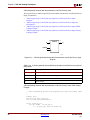
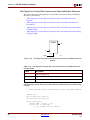
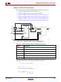
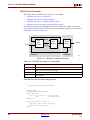
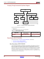
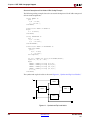
Grouping Through Incremental Synthesis Diagram . . . . . . . . . . . . . . . . . . . . . . . . . .
Resynthesize (RESYNTHESIZE) . . . . . . . . . . . . . . . . . . . . . . . . . . . . . . . . . . . . . . . . . . .
About Resynthesize (RESYNTHESIZE . . . . . . . . . . . . . . . . . . . . . . . . . . . . . . . . . . . . .
Resynthesize (RESYNTHESIZE) Examples. . . . . . . . . . . . . . . . . . . . . . . . . . . . . . . . . .
280
281
282
282
282
283
Speed Optimization Under Area Constraint . . . . . . . . . . . . . . . . . . . . . . . . . . . . . . . . 285
About Speed Optimization Under Area Constraint . . . . . . . . . . . . . . . . . . . . . . . . . . . 285
Speed Optimization Under Area Constraint Examples . . . . . . . . . . . . . . . . . . . . . . . . 285
FPGA Optimization Log File . . . . . . . . . . . . . . . . . . . . . . . . . . . . . . . . . . . . . . . . . . . . . . . 287
Design Optimization Report . . . . . . . . . . . . . . . . . . . . . . . . . . . . . . . . . . . . . . . . . . . . . .
Cell Usage Report . . . . . . . . . . . . . . . . . . . . . . . . . . . . . . . . . . . . . . . . . . . . . . . . . . . . . . .
BELS Cell Usage . . . . . . . . . . . . . . . . . . . . . . . . . . . . . . . . . . . . . . . . . . . . . . . . . . . . . .
Flip-Flops and Latches Cell Usage . . . . . . . . . . . . . . . . . . . . . . . . . . . . . . . . . . . . . . . .
RAMS Cell Usage . . . . . . . . . . . . . . . . . . . . . . . . . . . . . . . . . . . . . . . . . . . . . . . . . . . . .
SHIFTERS Cell Usage . . . . . . . . . . . . . . . . . . . . . . . . . . . . . . . . . . . . . . . . . . . . . . . . . .
Tristates Cell Usage . . . . . . . . . . . . . . . . . . . . . . . . . . . . . . . . . . . . . . . . . . . . . . . . . . .
Clock Buffers Cell Usage. . . . . . . . . . . . . . . . . . . . . . . . . . . . . . . . . . . . . . . . . . . . . . . .
IO Buffers Cell Usage . . . . . . . . . . . . . . . . . . . . . . . . . . . . . . . . . . . . . . . . . . . . . . . . . .
LOGICAL Cell Usage . . . . . . . . . . . . . . . . . . . . . . . . . . . . . . . . . . . . . . . . . . . . . . . . . .
OTHER Cell Usage . . . . . . . . . . . . . . . . . . . . . . . . . . . . . . . . . . . . . . . . . . . . . . . . . . . .
Timing Report . . . . . . . . . . . . . . . . . . . . . . . . . . . . . . . . . . . . . . . . . . . . . . . . . . . . . . . . . . .
About the Timing Report . . . . . . . . . . . . . . . . . . . . . . . . . . . . . . . . . . . . . . . . . . . . . . .
Timing Report Example . . . . . . . . . . . . . . . . . . . . . . . . . . . . . . . . . . . . . . . . . . . . . . . .
Timing Report Timing Summary Section . . . . . . . . . . . . . . . . . . . . . . . . . . . . . . . . . . .
Timing Report Timing Detail Section . . . . . . . . . . . . . . . . . . . . . . . . . . . . . . . . . . . . . .
Timing Report Schematic . . . . . . . . . . . . . . . . . . . . . . . . . . . . . . . . . . . . . . . . . . . . . . .
Timing Report Paths and Ports . . . . . . . . . . . . . . . . . . . . . . . . . . . . . . . . . . . . . . . . . . .
287
287
288
288
288
288
288
289
289
289
289
290
290
290
291
292
292
292
Implementation Constraints . . . . . . . . . . . . . . . . . . . . . . . . . . . . . . . . . . . . . . . . . . . . . . . . 293
Virtex Primitive Support . . . . . . . . . . . . . . . . . . . . . . . . . . . . . . . . . . . . . . . . . . . . . . . . . . . 293
Instantiating Virtex Primitives . . . . . . . . . . . . . . . . . . . . . . . . . . . . . . . . . . . . . . . . . . . . .
Generating Primitives Through Attributes . . . . . . . . . . . . . . . . . . . . . . . . . . . . . . . . . .
Primitives and Black Boxes . . . . . . . . . . . . . . . . . . . . . . . . . . . . . . . . . . . . . . . . . . . . . . . .
VHDL and Verilog Virtex Libraries . . . . . . . . . . . . . . . . . . . . . . . . . . . . . . . . . . . . . . . .
About VHDL and Verilog Virtex Libraries . . . . . . . . . . . . . . . . . . . . . . . . . . . . . . . . . .
VHDL Virtex Libraries . . . . . . . . . . . . . . . . . . . . . . . . . . . . . . . . . . . . . . . . . . . . . . . . .
Verilog Virtex Libraries . . . . . . . . . . . . . . . . . . . . . . . . . . . . . . . . . . . . . . . . . . . . . . . .
Virtex Primitives Log File . . . . . . . . . . . . . . . . . . . . . . . . . . . . . . . . . . . . . . . . . . . . . . . . .
Virtex Primitives Related Constraints . . . . . . . . . . . . . . . . . . . . . . . . . . . . . . . . . . . . . . .
Virtex Primitives Coding Examples . . . . . . . . . . . . . . . . . . . . . . . . . . . . . . . . . . . . . . . .
Using the UNIMACRO Library . . . . . . . . . . . . . . . . . . . . . . . . . . . . . . . . . . . . . . . . . . . .
293
294
294
295
295
295
295
296
296
296
298
Cores Processing . . . . . . . . . . . . . . . . . . . . . . . . . . . . . . . . . . . . . . . . . . . . . . . . . . . . . . . . . . . 298
About Cores Processing . . . . . . . . . . . . . . . . . . . . . . . . . . . . . . . . . . . . . . . . . . . . . . . . 298
Cores Processing VHDL Coding Example . . . . . . . . . . . . . . . . . . . . . . . . . . . . . . . . . . 299
Read Cores Enabled or Disabled . . . . . . . . . . . . . . . . . . . . . . . . . . . . . . . . . . . . . . . . . . 299
Specifying INIT and RLOC . . . . . . . . . . . . . . . . . . . . . . . . . . . . . . . . . . . . . . . . . . . . . . . . 300
About Specifying INIT and RLOC . . . . . . . . . . . . . . . . . . . . . . . . . . . . . . . . . . . . . . . . . 300
Passing an INIT Value Via the LUT_MAP Constraint Coding Examples . . . . . . . . . 300
Specifying INIT Value for a Flip-Flop Coding Examples . . . . . . . . . . . . . . . . . . . . . . 302
XST User Guide
10.1
www.xilinx.com
9
R
Specifying INIT and RLOC Values for a Flip-Flop Coding Examples . . . . . . . . . . . . 304
Using PCI Flow With XST . . . . . . . . . . . . . . . . . . . . . . . . . . . . . . . . . . . . . . . . . . . . . . . . . . 305
Satisfying Placement Constraints and Meeting Timing Requirements . . . . . . . . . . . 305
Preventing Logic and Flip-Flop Replication . . . . . . . . . . . . . . . . . . . . . . . . . . . . . . . . . 306
Disabling Read Cores . . . . . . . . . . . . . . . . . . . . . . . . . . . . . . . . . . . . . . . . . . . . . . . . . . . . 306
Chapter 4: XST CPLD Optimization
CPLD Synthesis Options . . . . . . . . . . . . . . . . . . . . . . . . . . . . . . . . . . . . . . . . . . . . . . . . . . . 307
About CPLD Synthesis Options. . . . . . . . . . . . . . . . . . . . . . . . . . . . . . . . . . . . . . . . . . . . 307
CPLD Synthesis Supported Devices . . . . . . . . . . . . . . . . . . . . . . . . . . . . . . . . . . . . . . . . 308
Setting CPLD Synthesis Options . . . . . . . . . . . . . . . . . . . . . . . . . . . . . . . . . . . . . . . . . . . 308
Implementation Details for Macro Generation . . . . . . . . . . . . . . . . . . . . . . . . . . . . . .
CPLD Synthesis Log File Analysis . . . . . . . . . . . . . . . . . . . . . . . . . . . . . . . . . . . . . . . . . .
CPLD Synthesis Constraints. . . . . . . . . . . . . . . . . . . . . . . . . . . . . . . . . . . . . . . . . . . . . . . .
Improving Results in CPLD Synthesis . . . . . . . . . . . . . . . . . . . . . . . . . . . . . . . . . . . . . .
308
309
311
311
About Improving Results in CPLD Synthesis . . . . . . . . . . . . . . . . . . . . . . . . . . . . . . . . 311
Obtaining Better Frequency . . . . . . . . . . . . . . . . . . . . . . . . . . . . . . . . . . . . . . . . . . . . . . . 311
Fitting a Large Design . . . . . . . . . . . . . . . . . . . . . . . . . . . . . . . . . . . . . . . . . . . . . . . . . . . . 312
Chapter 5: XST Design Constraints
About Constraints . . . . . . . . . . . . . . . . . . . . . . . . . . . . . . . . . . . . . . . . . . . . . . . . . . . . . . . . . . 315
List of XST Design Constraints . . . . . . . . . . . . . . . . . . . . . . . . . . . . . . . . . . . . . . . . . . . . . 316
XST General Constraints . . . . . . . . . . . . . . . . . . . . . . . . . . . . . . . . . . . . . . . . . . . . . . . . . .
XST HDL Constraints . . . . . . . . . . . . . . . . . . . . . . . . . . . . . . . . . . . . . . . . . . . . . . . . . . . .
XST FPGA Constraints (Non-Timing) . . . . . . . . . . . . . . . . . . . . . . . . . . . . . . . . . . . . . .
XST CPLD Constraints (Non-Timing) . . . . . . . . . . . . . . . . . . . . . . . . . . . . . . . . . . . . . .
XST Timing Constraints . . . . . . . . . . . . . . . . . . . . . . . . . . . . . . . . . . . . . . . . . . . . . . . . . .
XST Implementation Constraints . . . . . . . . . . . . . . . . . . . . . . . . . . . . . . . . . . . . . . . . . .
Third Party Constraints . . . . . . . . . . . . . . . . . . . . . . . . . . . . . . . . . . . . . . . . . . . . . . . . . . .
316
317
317
319
319
319
319
Setting Global Constraints and Options . . . . . . . . . . . . . . . . . . . . . . . . . . . . . . . . . . . . 320
Setting Synthesis Options . . . . . . . . . . . . . . . . . . . . . . . . . . . . . . . . . . . . . . . . . . . . . . . . .
Setting HDL Options . . . . . . . . . . . . . . . . . . . . . . . . . . . . . . . . . . . . . . . . . . . . . . . . . . . . .
Setting HDL Options for FPGA Devices . . . . . . . . . . . . . . . . . . . . . . . . . . . . . . . . . . . .
Setting HDL Options for CPLD Devices . . . . . . . . . . . . . . . . . . . . . . . . . . . . . . . . . . . .
Setting Xilinx-Specific Options . . . . . . . . . . . . . . . . . . . . . . . . . . . . . . . . . . . . . . . . . . . .
Setting Xilinx-Specific Options for FPGA Devices . . . . . . . . . . . . . . . . . . . . . . . . . . . .
Setting Xilinx-Specific Options for CPLD Devices . . . . . . . . . . . . . . . . . . . . . . . . . . . .
Setting Other XST Command Line Options . . . . . . . . . . . . . . . . . . . . . . . . . . . . . . . . . .
Custom Compile File List . . . . . . . . . . . . . . . . . . . . . . . . . . . . . . . . . . . . . . . . . . . . . . . . .
320
321
321
322
322
322
323
323
323
VHDL Attribute Syntax . . . . . . . . . . . . . . . . . . . . . . . . . . . . . . . . . . . . . . . . . . . . . . . . . . . . 324
Verilog-2001 Attributes . . . . . . . . . . . . . . . . . . . . . . . . . . . . . . . . . . . . . . . . . . . . . . . . . . . . . 324
About Verilog-2001 Attributes . . . . . . . . . . . . . . . . . . . . . . . . . . . . . . . . . . . . . . . . . . . . .
Verilog-2001 Attributes Syntax . . . . . . . . . . . . . . . . . . . . . . . . . . . . . . . . . . . . . . . . . . . .
Verilog-2001 Limitations . . . . . . . . . . . . . . . . . . . . . . . . . . . . . . . . . . . . . . . . . . . . . . . . . .
Verilog-2001 Meta Comments . . . . . . . . . . . . . . . . . . . . . . . . . . . . . . . . . . . . . . . . . . . . .
324
325
325
325
XST Constraint File (XCF) . . . . . . . . . . . . . . . . . . . . . . . . . . . . . . . . . . . . . . . . . . . . . . . . . . 326
Specifying the XST Constraint File (XCF) . . . . . . . . . . . . . . . . . . . . . . . . . . . . . . . . . . . . 326
XCF Syntax and Utilization . . . . . . . . . . . . . . . . . . . . . . . . . . . . . . . . . . . . . . . . . . . . . . . 326
Native and Non-Native User Constraint File (UCF) Constraints Syntax . . . . . . . . . 327
10
www.xilinx.com
XST User Guide
10.1
R
Native User Constraint File (UCF) Constraints. . . . . . . . . . . . . . . . . . . . . . . . . . . . . . . 327
Non-Native User Constraint File (UCF) Constraints . . . . . . . . . . . . . . . . . . . . . . . . . . 327
XCF Syntax Limitations. . . . . . . . . . . . . . . . . . . . . . . . . . . . . . . . . . . . . . . . . . . . . . . . . . . 328
Constraints Priority . . . . . . . . . . . . . . . . . . . . . . . . . . . . . . . . . . . . . . . . . . . . . . . . . . . . . . . . 328
XST-Specific Non-Timing Options . . . . . . . . . . . . . . . . . . . . . . . . . . . . . . . . . . . . . . . . . 328
XST Command Line Only Options . . . . . . . . . . . . . . . . . . . . . . . . . . . . . . . . . . . . . . . . . 334
XST Timing Options . . . . . . . . . . . . . . . . . . . . . . . . . . . . . . . . . . . . . . . . . . . . . . . . . . . . . 338
XST Timing Options: Project Navigator > Process Properties or Command Line . . 338
XST Timing Options: Xilinx Constraint File (XCF) . . . . . . . . . . . . . . . . . . . . . . . . . . . . 338
XST General Constraints . . . . . . . . . . . . . . . . . . . . . . . . . . . . . . . . . . . . . . . . . . . . . . . . . . . 339
Add I/O Buffers (–iobuf) . . . . . . . . . . . . . . . . . . . . . . . . . . . . . . . . . . . . . . . . . . . . . . . . .
Add I/O Buffers Architecture Support . . . . . . . . . . . . . . . . . . . . . . . . . . . . . . . . . . . . .
Add I/O Buffers Applicable Elements . . . . . . . . . . . . . . . . . . . . . . . . . . . . . . . . . . . . .
Add I/O Buffer Propagation Rules . . . . . . . . . . . . . . . . . . . . . . . . . . . . . . . . . . . . . . . .
Add I/O Buffers Syntax Examples . . . . . . . . . . . . . . . . . . . . . . . . . . . . . . . . . . . . . . . .
BoxType (BOX_TYPE) . . . . . . . . . . . . . . . . . . . . . . . . . . . . . . . . . . . . . . . . . . . . . . . . . . .
Box Type Architecture Support . . . . . . . . . . . . . . . . . . . . . . . . . . . . . . . . . . . . . . . . . .
Box Type Applicable Elements . . . . . . . . . . . . . . . . . . . . . . . . . . . . . . . . . . . . . . . . . . .
Box Type Propagation Rules . . . . . . . . . . . . . . . . . . . . . . . . . . . . . . . . . . . . . . . . . . . . .
Box Type Syntax Examples . . . . . . . . . . . . . . . . . . . . . . . . . . . . . . . . . . . . . . . . . . . . . .
Bus Delimiter (–bus_delimiter) . . . . . . . . . . . . . . . . . . . . . . . . . . . . . . . . . . . . . . . . . . .
Bus Delimiter Architecture Support . . . . . . . . . . . . . . . . . . . . . . . . . . . . . . . . . . . . . . .
Bus Delimiter Applicable Elements . . . . . . . . . . . . . . . . . . . . . . . . . . . . . . . . . . . . . . .
Bus Delimiter Propagation Rules . . . . . . . . . . . . . . . . . . . . . . . . . . . . . . . . . . . . . . . . .
Bus Delimiter Syntax Examples . . . . . . . . . . . . . . . . . . . . . . . . . . . . . . . . . . . . . . . . . .
Case (–case) . . . . . . . . . . . . . . . . . . . . . . . . . . . . . . . . . . . . . . . . . . . . . . . . . . . . . . . . . . . . .
Case Architecture Support . . . . . . . . . . . . . . . . . . . . . . . . . . . . . . . . . . . . . . . . . . . . . .
Case Applicable Elements . . . . . . . . . . . . . . . . . . . . . . . . . . . . . . . . . . . . . . . . . . . . . . .
Case Propagation Rules . . . . . . . . . . . . . . . . . . . . . . . . . . . . . . . . . . . . . . . . . . . . . . . .
Case Syntax Examples . . . . . . . . . . . . . . . . . . . . . . . . . . . . . . . . . . . . . . . . . . . . . . . . .
Case Implementation Style (–vlgcase) . . . . . . . . . . . . . . . . . . . . . . . . . . . . . . . . . . . . .
Case Implementation Style Architecture Support . . . . . . . . . . . . . . . . . . . . . . . . . . . . .
Case Implementation Style Applicable Elements . . . . . . . . . . . . . . . . . . . . . . . . . . . . .
Case Implementation Style Propagation Rules . . . . . . . . . . . . . . . . . . . . . . . . . . . . . . .
Case Implementation Style Syntax Examples . . . . . . . . . . . . . . . . . . . . . . . . . . . . . . . .
Verilog Macros (-define) . . . . . . . . . . . . . . . . . . . . . . . . . . . . . . . . . . . . . . . . . . . . . . . . . .
Verilog Macros Architecture Support . . . . . . . . . . . . . . . . . . . . . . . . . . . . . . . . . . . . . .
Verilog Macros Applicable Elements . . . . . . . . . . . . . . . . . . . . . . . . . . . . . . . . . . . . . .
Verilog Macros Propagation Rules . . . . . . . . . . . . . . . . . . . . . . . . . . . . . . . . . . . . . . . .
Verilog Macros Syntax Examples . . . . . . . . . . . . . . . . . . . . . . . . . . . . . . . . . . . . . . . . .
Duplication Suffix (–duplication_suffix) . . . . . . . . . . . . . . . . . . . . . . . . . . . . . . . . . . . .
Duplication Suffix Architecture Support . . . . . . . . . . . . . . . . . . . . . . . . . . . . . . . . . . .
Duplication Suffix Applicable Elements . . . . . . . . . . . . . . . . . . . . . . . . . . . . . . . . . . . .
Duplication Suffix Propagation Rules . . . . . . . . . . . . . . . . . . . . . . . . . . . . . . . . . . . . . .
Duplication Suffix Syntax Examples . . . . . . . . . . . . . . . . . . . . . . . . . . . . . . . . . . . . . . .
Full Case (FULL_CASE) . . . . . . . . . . . . . . . . . . . . . . . . . . . . . . . . . . . . . . . . . . . . . . . . . .
Full Case Architecture Support . . . . . . . . . . . . . . . . . . . . . . . . . . . . . . . . . . . . . . . . . . .
Full Case Applicable Elements . . . . . . . . . . . . . . . . . . . . . . . . . . . . . . . . . . . . . . . . . . .
Full Case Propagation Rules . . . . . . . . . . . . . . . . . . . . . . . . . . . . . . . . . . . . . . . . . . . . .
Full Case Syntax Examples . . . . . . . . . . . . . . . . . . . . . . . . . . . . . . . . . . . . . . . . . . . . . .
Generate RTL Schematic (–rtlview) . . . . . . . . . . . . . . . . . . . . . . . . . . . . . . . . . . . . . . .
Generate RTL Schematic Architecture Support . . . . . . . . . . . . . . . . . . . . . . . . . . . . . .
Generate RTL Schematic Applicable Elements . . . . . . . . . . . . . . . . . . . . . . . . . . . . . . .
XST User Guide
10.1
www.xilinx.com
340
340
340
340
340
341
341
341
341
341
342
342
342
342
342
343
343
343
343
343
343
344
344
344
344
344
344
344
345
345
345
346
346
346
346
346
347
347
347
347
348
348
348
11
R
Generate RTL Schematic Propagation Rules . . . . . . . . . . . . . . . . . . . . . . . . . . . . . . . . . 348
Generate RTL Schematic Syntax Examples . . . . . . . . . . . . . . . . . . . . . . . . . . . . . . . . . . 348
Generics (-generics) . . . . . . . . . . . . . . . . . . . . . . . . . . . . . . . . . . . . . . . . . . . . . . . . . . . . . .
Generics Architecture Support . . . . . . . . . . . . . . . . . . . . . . . . . . . . . . . . . . . . . . . . . . .
Generics Applicable Elements . . . . . . . . . . . . . . . . . . . . . . . . . . . . . . . . . . . . . . . . . . .
Generics Propagation Rules . . . . . . . . . . . . . . . . . . . . . . . . . . . . . . . . . . . . . . . . . . . . .
Generics Syntax Examples . . . . . . . . . . . . . . . . . . . . . . . . . . . . . . . . . . . . . . . . . . . . . .
Hierarchy Separator (–hierarchy_separator) . . . . . . . . . . . . . . . . . . . . . . . . . . . . . . . .
Hierarchy Separator Architecture Support . . . . . . . . . . . . . . . . . . . . . . . . . . . . . . . . . .
Hierarchy Separator Applicable Elements . . . . . . . . . . . . . . . . . . . . . . . . . . . . . . . . . .
Hierarchy Separator Propagation Rules . . . . . . . . . . . . . . . . . . . . . . . . . . . . . . . . . . . .
Hierarchy Separator Syntax Examples . . . . . . . . . . . . . . . . . . . . . . . . . . . . . . . . . . . . .
I/O Standard (IOSTANDARD) . . . . . . . . . . . . . . . . . . . . . . . . . . . . . . . . . . . . . . . . . . . .
Keep (KEEP) . . . . . . . . . . . . . . . . . . . . . . . . . . . . . . . . . . . . . . . . . . . . . . . . . . . . . . . . . . . .
Keep Hierarchy (KEEP_HIERARCHY) . . . . . . . . . . . . . . . . . . . . . . . . . . . . . . . . . . . . .
Keep Hierarchy Values . . . . . . . . . . . . . . . . . . . . . . . . . . . . . . . . . . . . . . . . . . . . . . . . .
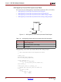
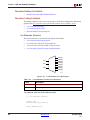
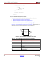
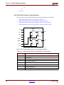
Preserving the Hierarchy . . . . . . . . . . . . . . . . . . . . . . . . . . . . . . . . . . . . . . . . . . . . . . .
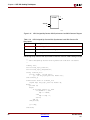
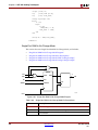
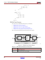
Keep Hierarchy Diagram . . . . . . . . . . . . . . . . . . . . . . . . . . . . . . . . . . . . . . . . . . . . . . .
Keep Hierarchy Architecture Support . . . . . . . . . . . . . . . . . . . . . . . . . . . . . . . . . . . . .
Keep Hierarchy Applicable Elements . . . . . . . . . . . . . . . . . . . . . . . . . . . . . . . . . . . . . .
Keep Hierarchy Propagation Rules . . . . . . . . . . . . . . . . . . . . . . . . . . . . . . . . . . . . . . . .
Keep Hierarchy Syntax Examples . . . . . . . . . . . . . . . . . . . . . . . . . . . . . . . . . . . . . . . . .
Library Search Order (–lso) . . . . . . . . . . . . . . . . . . . . . . . . . . . . . . . . . . . . . . . . . . . . . . .
Library Search Order Architecture Support . . . . . . . . . . . . . . . . . . . . . . . . . . . . . . . . .
Library Search Order Applicable Elements . . . . . . . . . . . . . . . . . . . . . . . . . . . . . . . . .
Library Search Order Propagation Rules . . . . . . . . . . . . . . . . . . . . . . . . . . . . . . . . . . .
Library Search Order Syntax Examples . . . . . . . . . . . . . . . . . . . . . . . . . . . . . . . . . . . .
LOC . . . . . . . . . . . . . . . . . . . . . . . . . . . . . . . . . . . . . . . . . . . . . . . . . . . . . . . . . . . . . . . . . . .
Netlist Hierarchy (-netlist_hierarchy) . . . . . . . . . . . . . . . . . . . . . . . . . . . . . . . . . . . . . . .
Netlist Hierarchy Architecture Support . . . . . . . . . . . . . . . . . . . . . . . . . . . . . . . . . . . .
Netlist Hierarchy Applicable Elements. . . . . . . . . . . . . . . . . . . . . . . . . . . . . . . . . . . . .
Netlist Hierarchy Propagation Rules . . . . . . . . . . . . . . . . . . . . . . . . . . . . . . . . . . . . . .
Netlist Hierarchy Syntax Examples . . . . . . . . . . . . . . . . . . . . . . . . . . . . . . . . . . . . . . .
Optimization Effort (OPT_LEVEL) . . . . . . . . . . . . . . . . . . . . . . . . . . . . . . . . . . . . . . . .
Optimization Effort Architecture Support . . . . . . . . . . . . . . . . . . . . . . . . . . . . . . . . . .
Optimization Effort Applicable Elements . . . . . . . . . . . . . . . . . . . . . . . . . . . . . . . . . . .
Optimization Effort Propagation Rules . . . . . . . . . . . . . . . . . . . . . . . . . . . . . . . . . . . .
Optimization Effort Syntax Examples . . . . . . . . . . . . . . . . . . . . . . . . . . . . . . . . . . . . . .
Optimization Goal (OPT_MODE) . . . . . . . . . . . . . . . . . . . . . . . . . . . . . . . . . . . . . . . . .
Optimization Goal Architecture Support . . . . . . . . . . . . . . . . . . . . . . . . . . . . . . . . . . .
Optimization Goal Applicable Elements . . . . . . . . . . . . . . . . . . . . . . . . . . . . . . . . . . .
Optimization Goal Propagation Rules . . . . . . . . . . . . . . . . . . . . . . . . . . . . . . . . . . . . .
Optimization Goal Syntax Examples . . . . . . . . . . . . . . . . . . . . . . . . . . . . . . . . . . . . . .
Parallel Case (PARALLEL_CASE) . . . . . . . . . . . . . . . . . . . . . . . . . . . . . . . . . . . . . . . . .
Parallel Case Architecture Support . . . . . . . . . . . . . . . . . . . . . . . . . . . . . . . . . . . . . . . .
Parallel Case Applicable Elements . . . . . . . . . . . . . . . . . . . . . . . . . . . . . . . . . . . . . . . .
Parallel Case Propagation Rules . . . . . . . . . . . . . . . . . . . . . . . . . . . . . . . . . . . . . . . . . .
Parallel Case Syntax Examples . . . . . . . . . . . . . . . . . . . . . . . . . . . . . . . . . . . . . . . . . . .
RLOC . . . . . . . . . . . . . . . . . . . . . . . . . . . . . . . . . . . . . . . . . . . . . . . . . . . . . . . . . . . . . . . . . .
Save (S / SAVE) . . . . . . . . . . . . . . . . . . . . . . . . . . . . . . . . . . . . . . . . . . . . . . . . . . . . . . . . .
Synthesis Constraint File (–uc) . . . . . . . . . . . . . . . . . . . . . . . . . . . . . . . . . . . . . . . . . . . .
Synthesis Constraint File Architecture Support . . . . . . . . . . . . . . . . . . . . . . . . . . . . . .
Synthesis Constraint File Applicable Elements . . . . . . . . . . . . . . . . . . . . . . . . . . . . . . .
Synthesis Constraint File Propagation Rules . . . . . . . . . . . . . . . . . . . . . . . . . . . . . . . .
12
www.xilinx.com
348
349
349
349
349
350
350
350
350
350
351
351
351
351
352
352
352
352
352
353
353
353
354
354
354
354
354
354
355
355
355
355
355
355
355
355
356
356
356
356
357
357
357
357
357
358
358
358
359
359
359
359
XST User Guide
10.1
R
Synthesis Constraint File Syntax Examples . . . . . . . . . . . . . . . . . . . . . . . . . . . . . . . . .
Translate Off (TRANSLATE_OFF) and Translate On (TRANSLATE_ON) . . . . .
Translate Off and Translate On Architecture Support . . . . . . . . . . . . . . . . . . . . . . . . .
Translate Off and Translate On Applicable Elements . . . . . . . . . . . . . . . . . . . . . . . . . .
Translate Off and Translate On Propagation Rules . . . . . . . . . . . . . . . . . . . . . . . . . . .
Translate Off and Translate On Syntax Examples. . . . . . . . . . . . . . . . . . . . . . . . . . . . .
Use Synthesis Constraints File (–iuc) . . . . . . . . . . . . . . . . . . . . . . . . . . . . . . . . . . . . . .
Use Synthesis Constraints File Architecture Support . . . . . . . . . . . . . . . . . . . . . . . . . .
Use Synthesis Constraints File Applicable Elements . . . . . . . . . . . . . . . . . . . . . . . . . .
Use Synthesis Constraints File Propagation Rules . . . . . . . . . . . . . . . . . . . . . . . . . . . .
Use Synthesis Constraints File Syntax Examples . . . . . . . . . . . . . . . . . . . . . . . . . . . . .
Verilog Include Directories (–vlgincdir) . . . . . . . . . . . . . . . . . . . . . . . . . . . . . . . . . . .
Verilog Include Directories Architecture Support . . . . . . . . . . . . . . . . . . . . . . . . . . . .
Verilog Include Directories Applicable Elements . . . . . . . . . . . . . . . . . . . . . . . . . . . . .
Verilog Include Directories Propagation Rules . . . . . . . . . . . . . . . . . . . . . . . . . . . . . . .
Verilog Include Directories Syntax Examples . . . . . . . . . . . . . . . . . . . . . . . . . . . . . . . .
Verilog 2001 (–verilog2001) . . . . . . . . . . . . . . . . . . . . . . . . . . . . . . . . . . . . . . . . . . . . . . .
Verilog 2001 Architecture Support . . . . . . . . . . . . . . . . . . . . . . . . . . . . . . . . . . . . . . . .
Verilog 2001 Applicable Elements . . . . . . . . . . . . . . . . . . . . . . . . . . . . . . . . . . . . . . . .
Verilog 2001 Propagation Rules . . . . . . . . . . . . . . . . . . . . . . . . . . . . . . . . . . . . . . . . . .
Verilog 2001 Syntax Examples . . . . . . . . . . . . . . . . . . . . . . . . . . . . . . . . . . . . . . . . . . .
HDL Library Mapping File (–xsthdpini) . . . . . . . . . . . . . . . . . . . . . . . . . . . . . . . . . . .
HDL Library Mapping File Architecture Support . . . . . . . . . . . . . . . . . . . . . . . . . . . .
HDL Library Mapping File Applicable Elements . . . . . . . . . . . . . . . . . . . . . . . . . . . . .
HDL Library Mapping File Propagation Rules . . . . . . . . . . . . . . . . . . . . . . . . . . . . . . .
HDL Library Mapping File Syntax Examples . . . . . . . . . . . . . . . . . . . . . . . . . . . . . . . .
Work Directory (–xsthdpdir). . . . . . . . . . . . . . . . . . . . . . . . . . . . . . . . . . . . . . . . . . . . . .
Work Directory Example . . . . . . . . . . . . . . . . . . . . . . . . . . . . . . . . . . . . . . . . . . . . . . .
Work Directory Architecture Support . . . . . . . . . . . . . . . . . . . . . . . . . . . . . . . . . . . . .
Work Directory Applicable Elements . . . . . . . . . . . . . . . . . . . . . . . . . . . . . . . . . . . . . .
Work Directory Propagation Rules . . . . . . . . . . . . . . . . . . . . . . . . . . . . . . . . . . . . . . . .
Work Directory Syntax Examples . . . . . . . . . . . . . . . . . . . . . . . . . . . . . . . . . . . . . . . . .
359
359
360
360
360
360
360
360
360
360
361
361
361
361
361
361
362
362
362
362
362
362
363
363
363
363
364
364
365
365
365
365
XST HDL Constraints . . . . . . . . . . . . . . . . . . . . . . . . . . . . . . . . . . . . . . . . . . . . . . . . . . . . . . 365
About XST HDL Constraints . . . . . . . . . . . . . . . . . . . . . . . . . . . . . . . . . . . . . . . . . . . . . .
Automatic FSM Extraction (FSM_EXTRACT) . . . . . . . . . . . . . . . . . . . . . . . . . . . . . . . .
Automatic FSM Extraction Architecture Support . . . . . . . . . . . . . . . . . . . . . . . . . . . . .
Automatic FSM Extraction Applicable Elements . . . . . . . . . . . . . . . . . . . . . . . . . . . . .
Automatic FSM Extraction Propagation Rules . . . . . . . . . . . . . . . . . . . . . . . . . . . . . . .
Automatic FSM Extraction Syntax Examples . . . . . . . . . . . . . . . . . . . . . . . . . . . . . . . .
Enumerated Encoding (ENUM_ENCODING) . . . . . . . . . . . . . . . . . . . . . . . . . . . . . .
Enumerated Encoding Architecture Support . . . . . . . . . . . . . . . . . . . . . . . . . . . . . . . .
Enumerated Encoding Applicable Elements . . . . . . . . . . . . . . . . . . . . . . . . . . . . . . . .
Enumerated Encoding Propagation Rules . . . . . . . . . . . . . . . . . . . . . . . . . . . . . . . . . .
Enumerated Encoding Syntax Examples . . . . . . . . . . . . . . . . . . . . . . . . . . . . . . . . . . .
Equivalent Register Removal (EQUIVALENT_REGISTER_REMOVAL) . . . . . .
Equivalent Register Removal Architecture Support . . . . . . . . . . . . . . . . . . . . . . . . . . .
Equivalent Register Removal Applicable Elements . . . . . . . . . . . . . . . . . . . . . . . . . . .
Equivalent Register Removal Propagation Rules . . . . . . . . . . . . . . . . . . . . . . . . . . . . .
Equivalent Register Removal Syntax Examples . . . . . . . . . . . . . . . . . . . . . . . . . . . . . .
FSM Encoding Algorithm (FSM_ENCODING) . . . . . . . . . . . . . . . . . . . . . . . . . . . . .
FSM Encoding Algorithm Architecture Support . . . . . . . . . . . . . . . . . . . . . . . . . . . . .
FSM Encoding Algorithm Applicable Elements . . . . . . . . . . . . . . . . . . . . . . . . . . . . . .
FSM Encoding Algorithm Propagation Rules . . . . . . . . . . . . . . . . . . . . . . . . . . . . . . . .
XST User Guide
10.1
www.xilinx.com
366
366
366
366
366
366
367
367
367
367
367
368
368
368
368
369
369
370
370
370
13
R
FSM Encoding Algorithm Syntax Examples . . . . . . . . . . . . . . . . . . . . . . . . . . . . . . . . .
Mux Extraction (MUX_EXTRACT) . . . . . . . . . . . . . . . . . . . . . . . . . . . . . . . . . . . . . . . .
Mux Extraction Architecture Support . . . . . . . . . . . . . . . . . . . . . . . . . . . . . . . . . . . . . .
Mux Extraction Applicable Elements . . . . . . . . . . . . . . . . . . . . . . . . . . . . . . . . . . . . . .
Mux Extraction Propagation Rules . . . . . . . . . . . . . . . . . . . . . . . . . . . . . . . . . . . . . . . .
Mux Extraction Syntax Examples . . . . . . . . . . . . . . . . . . . . . . . . . . . . . . . . . . . . . . . . .
Register Power Up (REGISTER_POWERUP) . . . . . . . . . . . . . . . . . . . . . . . . . . . . . . .
Register Power Up Architecture Support . . . . . . . . . . . . . . . . . . . . . . . . . . . . . . . . . . .
Register Power Up Applicable Elements . . . . . . . . . . . . . . . . . . . . . . . . . . . . . . . . . . .
Register Power Up Propagation Rules . . . . . . . . . . . . . . . . . . . . . . . . . . . . . . . . . . . . .
Register Power Up Syntax Examples . . . . . . . . . . . . . . . . . . . . . . . . . . . . . . . . . . . . . .
Resource Sharing (RESOURCE_SHARING) . . . . . . . . . . . . . . . . . . . . . . . . . . . . . . . . .
Resource Sharing Architecture Support . . . . . . . . . . . . . . . . . . . . . . . . . . . . . . . . . . . .
Resource Sharing Applicable Elements . . . . . . . . . . . . . . . . . . . . . . . . . . . . . . . . . . . .
Resource Sharing Propagation Rules . . . . . . . . . . . . . . . . . . . . . . . . . . . . . . . . . . . . . .
Resource Sharing Syntax Examples . . . . . . . . . . . . . . . . . . . . . . . . . . . . . . . . . . . . . . .
Safe Recovery State (SAFE_RECOVERY_STATE) . . . . . . . . . . . . . . . . . . . . . . . . . . . .
Safe Recovery State Architecture Support . . . . . . . . . . . . . . . . . . . . . . . . . . . . . . . . . .
Safe Recovery State Applicable Elements . . . . . . . . . . . . . . . . . . . . . . . . . . . . . . . . . . .
Safe Recovery State Propagation Rules . . . . . . . . . . . . . . . . . . . . . . . . . . . . . . . . . . . . .
Safe Recovery State Syntax Examples . . . . . . . . . . . . . . . . . . . . . . . . . . . . . . . . . . . . . .
Safe Implementation (SAFE_IMPLEMENTATION) . . . . . . . . . . . . . . . . . . . . . . . . . .
Safe Implementation Architecture Support . . . . . . . . . . . . . . . . . . . . . . . . . . . . . . . . .
Safe Implementation Applicable Elements . . . . . . . . . . . . . . . . . . . . . . . . . . . . . . . . . .
Safe Implementation Propagation Rules . . . . . . . . . . . . . . . . . . . . . . . . . . . . . . . . . . . .
Safe Implementation Syntax Examples . . . . . . . . . . . . . . . . . . . . . . . . . . . . . . . . . . . . .
Signal Encoding (SIGNAL_ENCODING) . . . . . . . . . . . . . . . . . . . . . . . . . . . . . . . . . .
Signal Encoding Architecture Support . . . . . . . . . . . . . . . . . . . . . . . . . . . . . . . . . . . . .
Signal Encoding Applicable Elements . . . . . . . . . . . . . . . . . . . . . . . . . . . . . . . . . . . . .
Signal Encoding Propagation Rules . . . . . . . . . . . . . . . . . . . . . . . . . . . . . . . . . . . . . . .
Signal Encoding Syntax Examples . . . . . . . . . . . . . . . . . . . . . . . . . . . . . . . . . . . . . . . .
370
371
371
371
371
371
372
372
372
373
373
374
374
374
374
374
375
375
375
375
375
376
376
376
376
376
377
377
377
378
378
XST FPGA Constraints (Non-Timing) . . . . . . . . . . . . . . . . . . . . . . . . . . . . . . . . . . . . . . 378
Asynchronous to Synchronous (ASYNC_TO_SYNC) . . . . . . . . . . . . . . . . . . . . . . . . .
Asynchronous to Synchronous Architecture Support . . . . . . . . . . . . . . . . . . . . . . . . .
Asynchronous to Synchronous Applicable Elements . . . . . . . . . . . . . . . . . . . . . . . . . .
Asynchronous to Synchronous Propagation Rules . . . . . . . . . . . . . . . . . . . . . . . . . . . .
Asynchronous to Synchronous Syntax Examples . . . . . . . . . . . . . . . . . . . . . . . . . . . . .
Automatic BRAM Packing (AUTO_BRAM_PACKING) . . . . . . . . . . . . . . . . . . . . . . .
Automatic BRAM Packing Architecture Support . . . . . . . . . . . . . . . . . . . . . . . . . . . . .
Automatic BRAM Packing Applicable Elements . . . . . . . . . . . . . . . . . . . . . . . . . . . . .
Automatic BRAM Packing Propagation Rules . . . . . . . . . . . . . . . . . . . . . . . . . . . . . . .
Automatic BRAM Packing Syntax Examples . . . . . . . . . . . . . . . . . . . . . . . . . . . . . . . .
BRAM Utilization Ratio (BRAM_UTILIZATION_RATIO) . . . . . . . . . . . . . . . . . . . . .
BRAM Utilization Ratio Architecture Support . . . . . . . . . . . . . . . . . . . . . . . . . . . . . . .
BRAM Utilization Ratio Applicable Elements . . . . . . . . . . . . . . . . . . . . . . . . . . . . . . .
BRAM Utilization Ratio Propagation Rules . . . . . . . . . . . . . . . . . . . . . . . . . . . . . . . . .
BRAM Utilization Ratio Syntax Examples . . . . . . . . . . . . . . . . . . . . . . . . . . . . . . . . . .
Buffer Type (BUFFER_TYPE) . . . . . . . . . . . . . . . . . . . . . . . . . . . . . . . . . . . . . . . . . . . . .
Buffer Type Architecture Support . . . . . . . . . . . . . . . . . . . . . . . . . . . . . . . . . . . . . . . .
Buffer Type Applicable Elements . . . . . . . . . . . . . . . . . . . . . . . . . . . . . . . . . . . . . . . . .
Buffer Type Propagation Rules . . . . . . . . . . . . . . . . . . . . . . . . . . . . . . . . . . . . . . . . . . .
Buffer Type Syntax Examples . . . . . . . . . . . . . . . . . . . . . . . . . . . . . . . . . . . . . . . . . . . .
Extract BUFGCE (BUFGCE) . . . . . . . . . . . . . . . . . . . . . . . . . . . . . . . . . . . . . . . . . . . . . .
14
www.xilinx.com
380
380
381
381
381
381
381
381
381
381
382
382
382
382
382
383
383
383
384
384
384
XST User Guide
10.1
R
Extract BUFGCE Architecture Support . . . . . . . . . . . . . . . . . . . . . . . . . . . . . . . . . . . . .
Extract BUFGCE Applicable Elements . . . . . . . . . . . . . . . . . . . . . . . . . . . . . . . . . . . . .
Extract BUFGCE Propagation Rules . . . . . . . . . . . . . . . . . . . . . . . . . . . . . . . . . . . . . . .
Extract BUFGCE Syntax Examples . . . . . . . . . . . . . . . . . . . . . . . . . . . . . . . . . . . . . . . .
Cores Search Directories (–sd) . . . . . . . . . . . . . . . . . . . . . . . . . . . . . . . . . . . . . . . . . . . .
Cores Search Directories Architecture Support . . . . . . . . . . . . . . . . . . . . . . . . . . . . . .
Cores Search Directories Applicable Elements . . . . . . . . . . . . . . . . . . . . . . . . . . . . . . .
Cores Search Directories Propagation Rules . . . . . . . . . . . . . . . . . . . . . . . . . . . . . . . . .
Cores Search Directories Syntax Examples . . . . . . . . . . . . . . . . . . . . . . . . . . . . . . . . . .
Decoder Extraction (DECODER_EXTRACT) . . . . . . . . . . . . . . . . . . . . . . . . . . . . . . .
Decoder Extraction Architecture Support . . . . . . . . . . . . . . . . . . . . . . . . . . . . . . . . . . .
Decoder Extraction Applicable Elements . . . . . . . . . . . . . . . . . . . . . . . . . . . . . . . . . . .
Decoder Extraction Propagation Rules . . . . . . . . . . . . . . . . . . . . . . . . . . . . . . . . . . . . .
Decoder Extraction Syntax Examples . . . . . . . . . . . . . . . . . . . . . . . . . . . . . . . . . . . . . .
DSP Utilization Ratio (DSP_UTILIZATION_RATIO) . . . . . . . . . . . . . . . . . . . . . . . . .
DSP Utilization Ratio Architecture Support . . . . . . . . . . . . . . . . . . . . . . . . . . . . . . . . .
DSP Utilization Ratio Applicable Elements . . . . . . . . . . . . . . . . . . . . . . . . . . . . . . . . .
DSP Utilization Ratio Propagation Rules . . . . . . . . . . . . . . . . . . . . . . . . . . . . . . . . . . .
DSP Utilization Ratio Syntax Examples . . . . . . . . . . . . . . . . . . . . . . . . . . . . . . . . . . . .
FSM Style (FSM_STYLE). . . . . . . . . . . . . . . . . . . . . . . . . . . . . . . . . . . . . . . . . . . . . . . . .
FSM Style Architecture Support . . . . . . . . . . . . . . . . . . . . . . . . . . . . . . . . . . . . . . . . . .
FSM Style Applicable Elements . . . . . . . . . . . . . . . . . . . . . . . . . . . . . . . . . . . . . . . . . .
FSM Style Propagation Rules . . . . . . . . . . . . . . . . . . . . . . . . . . . . . . . . . . . . . . . . . . . .
FSM Style Syntax Examples . . . . . . . . . . . . . . . . . . . . . . . . . . . . . . . . . . . . . . . . . . . . .
Power Reduction (POWER) . . . . . . . . . . . . . . . . . . . . . . . . . . . . . . . . . . . . . . . . . . . . . . .
Power Reduction Architecture Support . . . . . . . . . . . . . . . . . . . . . . . . . . . . . . . . . . . .
Power Reduction Applicable Elements . . . . . . . . . . . . . . . . . . . . . . . . . . . . . . . . . . . . .
Power Reduction Propagation Rules . . . . . . . . . . . . . . . . . . . . . . . . . . . . . . . . . . . . . .
Power Reduction Syntax Examples . . . . . . . . . . . . . . . . . . . . . . . . . . . . . . . . . . . . . . .
Read Cores (READ_CORES) . . . . . . . . . . . . . . . . . . . . . . . . . . . . . . . . . . . . . . . . . . . . . .
Read Cores Architecture Support . . . . . . . . . . . . . . . . . . . . . . . . . . . . . . . . . . . . . . . . .
Read Cores Applicable Elements . . . . . . . . . . . . . . . . . . . . . . . . . . . . . . . . . . . . . . . . .
Read Cores Propagation Rules . . . . . . . . . . . . . . . . . . . . . . . . . . . . . . . . . . . . . . . . . . .
Read Cores Syntax Examples . . . . . . . . . . . . . . . . . . . . . . . . . . . . . . . . . . . . . . . . . . . .
Resynthesize (RESYNTHESIZE) . . . . . . . . . . . . . . . . . . . . . . . . . . . . . . . . . . . . . . . . . .
Resynthesize Architecture Support. . . . . . . . . . . . . . . . . . . . . . . . . . . . . . . . . . . . . . . .
Resynthesize Applicable Elements . . . . . . . . . . . . . . . . . . . . . . . . . . . . . . . . . . . . . . . .
Resynthesize Propagation Rules . . . . . . . . . . . . . . . . . . . . . . . . . . . . . . . . . . . . . . . . . .
Resynthesize Syntax Examples . . . . . . . . . . . . . . . . . . . . . . . . . . . . . . . . . . . . . . . . . . .
Incremental Synthesis (INCREMENTAL_SYNTHESIS) . . . . . . . . . . . . . . . . . . . . .
Incremental Synthesis Architecture Support . . . . . . . . . . . . . . . . . . . . . . . . . . . . . . . .
Incremental Synthesis Applicable Elements . . . . . . . . . . . . . . . . . . . . . . . . . . . . . . . . .
Incremental Synthesis Propagation Rules . . . . . . . . . . . . . . . . . . . . . . . . . . . . . . . . . . .
Incremental Synthesis Syntax Examples . . . . . . . . . . . . . . . . . . . . . . . . . . . . . . . . . . . .
Logical Shifter Extraction (SHIFT_EXTRACT) . . . . . . . . . . . . . . . . . . . . . . . . . . . . . .
Logical Shifter Extraction Architecture Support . . . . . . . . . . . . . . . . . . . . . . . . . . . . . .
Logical Shifter Extraction Applicable Elements . . . . . . . . . . . . . . . . . . . . . . . . . . . . . .
Logical Shifter Extraction Propagation Rules . . . . . . . . . . . . . . . . . . . . . . . . . . . . . . . .
Logical Shifter Extraction Syntax Examples . . . . . . . . . . . . . . . . . . . . . . . . . . . . . . . . .
LUT Combining (LC) . . . . . . . . . . . . . . . . . . . . . . . . . . . . . . . . . . . . . . . . . . . . . . . . . . . . .
LUT Combining Architecture Support . . . . . . . . . . . . . . . . . . . . . . . . . . . . . . . . . . . . .
LUT Combining Applicable Elements . . . . . . . . . . . . . . . . . . . . . . . . . . . . . . . . . . . . .
LUT Combining Propagation Rules . . . . . . . . . . . . . . . . . . . . . . . . . . . . . . . . . . . . . . .
LUT Combining Syntax Examples . . . . . . . . . . . . . . . . . . . . . . . . . . . . . . . . . . . . . . . .
XST User Guide
10.1
www.xilinx.com
384
385
385
385
385
385
385
385
386
386
386
386
386
386
387
388
388
388
388
389
389
389
389
389
390
390
390
390
390
391
392
392
392
392
393
393
393
393
393
394
394
394
394
394
395
395
395
395
395
396
396
396
396
396
15
R
Map Logic on BRAM (BRAM_MAP) . . . . . . . . . . . . . . . . . . . . . . . . . . . . . . . . . . . . . .
Map Logic on BRAM Architecture Support . . . . . . . . . . . . . . . . . . . . . . . . . . . . . . . . .
Map Logic on BRAM Applicable Elements. . . . . . . . . . . . . . . . . . . . . . . . . . . . . . . . . .
Map Logic on BRAM Propagation Rules . . . . . . . . . . . . . . . . . . . . . . . . . . . . . . . . . . .
Map Logic on BRAM Syntax Examples . . . . . . . . . . . . . . . . . . . . . . . . . . . . . . . . . . . .
Max Fanout (MAX_FANOUT) . . . . . . . . . . . . . . . . . . . . . . . . . . . . . . . . . . . . . . . . . . . .
Max Fanout Architecture Support . . . . . . . . . . . . . . . . . . . . . . . . . . . . . . . . . . . . . . . .
Max Fanout Applicable Elements . . . . . . . . . . . . . . . . . . . . . . . . . . . . . . . . . . . . . . . . .
Max Fanout Propagation Rules . . . . . . . . . . . . . . . . . . . . . . . . . . . . . . . . . . . . . . . . . . .
Max Fanout Syntax Examples . . . . . . . . . . . . . . . . . . . . . . . . . . . . . . . . . . . . . . . . . . . .
Move First Stage (MOVE_FIRST_STAGE) . . . . . . . . . . . . . . . . . . . . . . . . . . . . . . . . .
Move First Stage Architecture Support . . . . . . . . . . . . . . . . . . . . . . . . . . . . . . . . . . . . .
Move First Stage Applicable Elements . . . . . . . . . . . . . . . . . . . . . . . . . . . . . . . . . . . . .
Move First Stage Propagation Rules . . . . . . . . . . . . . . . . . . . . . . . . . . . . . . . . . . . . . . .
Move First Stage Syntax Examples . . . . . . . . . . . . . . . . . . . . . . . . . . . . . . . . . . . . . . . .
Move Last Stage (MOVE_LAST_STAGE) . . . . . . . . . . . . . . . . . . . . . . . . . . . . . . . . . .
Move Last Stage Architecture Support . . . . . . . . . . . . . . . . . . . . . . . . . . . . . . . . . . . . .
Move Last Stage Applicable Elements . . . . . . . . . . . . . . . . . . . . . . . . . . . . . . . . . . . . .
Move Last Stage Propagation Rules . . . . . . . . . . . . . . . . . . . . . . . . . . . . . . . . . . . . . . .
Move Last Stage Syntax Examples . . . . . . . . . . . . . . . . . . . . . . . . . . . . . . . . . . . . . . . .
Multiplier Style (MULT_STYLE). . . . . . . . . . . . . . . . . . . . . . . . . . . . . . . . . . . . . . . . . .
Multiplier Style Architecture Support . . . . . . . . . . . . . . . . . . . . . . . . . . . . . . . . . . . . .
Multiplier Style Applicable Elements . . . . . . . . . . . . . . . . . . . . . . . . . . . . . . . . . . . . . .
Multiplier Style Propagation Rules . . . . . . . . . . . . . . . . . . . . . . . . . . . . . . . . . . . . . . . .
Multiplier Style Syntax Examples . . . . . . . . . . . . . . . . . . . . . . . . . . . . . . . . . . . . . . . . .
Mux Style (MUX_STYLE) . . . . . . . . . . . . . . . . . . . . . . . . . . . . . . . . . . . . . . . . . . . . . . . .
Mux Style Architecture Support . . . . . . . . . . . . . . . . . . . . . . . . . . . . . . . . . . . . . . . . . .
Mux Style Applicable Elements . . . . . . . . . . . . . . . . . . . . . . . . . . . . . . . . . . . . . . . . . .
Mux Style Propagation Rules . . . . . . . . . . . . . . . . . . . . . . . . . . . . . . . . . . . . . . . . . . . .
Mux Style Syntax Examples . . . . . . . . . . . . . . . . . . . . . . . . . . . . . . . . . . . . . . . . . . . . .
Number of Global Clock Buffers (–bufg) . . . . . . . . . . . . . . . . . . . . . . . . . . . . . . . . . . . .
Number of Global Clock Buffers Architecture Support . . . . . . . . . . . . . . . . . . . . . . . .
Number of Global Clock Buffers Applicable Elements . . . . . . . . . . . . . . . . . . . . . . . . .
Number of Global Clock Buffers Propagation Rules . . . . . . . . . . . . . . . . . . . . . . . . . .
Number of Global Clock Buffers Syntax Examples. . . . . . . . . . . . . . . . . . . . . . . . . . . .
Number of Regional Clock Buffers (–bufr) . . . . . . . . . . . . . . . . . . . . . . . . . . . . . . . . .
Number of Regional Clock Buffers Architecture Support. . . . . . . . . . . . . . . . . . . . . . .
Number of Regional Clock Buffers Applicable Elements . . . . . . . . . . . . . . . . . . . . . . .
Number of Regional Clock Buffers Propagation Rules . . . . . . . . . . . . . . . . . . . . . . . . .
Number of Regional Clock Buffers Syntax Examples . . . . . . . . . . . . . . . . . . . . . . . . . .
Optimize Instantiated Primitives (OPTIMIZE_PRIMITIVES) . . . . . . . . . . . . . . . .
Optimize Instantiated Primitives Architecture Support . . . . . . . . . . . . . . . . . . . . . . . .
Optimize Instantiated Primitives Applicable Elements . . . . . . . . . . . . . . . . . . . . . . . .
Optimize Instantiated Primitives Propagation Rules . . . . . . . . . . . . . . . . . . . . . . . . . .
Optimize Instantiated Primitives Syntax Examples . . . . . . . . . . . . . . . . . . . . . . . . . . .
Pack I/O Registers Into IOBs (IOB) . . . . . . . . . . . . . . . . . . . . . . . . . . . . . . . . . . . . . . . . .
Priority Encoder Extraction (PRIORITY_EXTRACT) . . . . . . . . . . . . . . . . . . . . . . . .
Priority Encoder Extraction Architecture Support . . . . . . . . . . . . . . . . . . . . . . . . . . . .
Priority Encoder Extraction Applicable Elements . . . . . . . . . . . . . . . . . . . . . . . . . . . . .
Priority Encoder Extraction Propagation Rules . . . . . . . . . . . . . . . . . . . . . . . . . . . . . .
Priority Encoder Extraction Syntax Examples . . . . . . . . . . . . . . . . . . . . . . . . . . . . . . .
RAM Extraction (RAM_EXTRACT) . . . . . . . . . . . . . . . . . . . . . . . . . . . . . . . . . . . . . . .
RAM Extraction Architecture Support . . . . . . . . . . . . . . . . . . . . . . . . . . . . . . . . . . . . .
RAM Extraction Applicable Elements . . . . . . . . . . . . . . . . . . . . . . . . . . . . . . . . . . . . .
16
www.xilinx.com
397
397
397
397
397
398
399
399
399
399
399
400
401
401
401
402
402
402
402
402
403
403
403
403
404
405
405
406
406
406
406
407
407
407
407
408
408
408
408
408
408
409
409
409
409
410
410
410
410
410
411
411
411
412
XST User Guide
10.1
R
RAM Extraction Propagation Rules . . . . . . . . . . . . . . . . . . . . . . . . . . . . . . . . . . . . . . . 412
RAM Extraction Syntax Examples . . . . . . . . . . . . . . . . . . . . . . . . . . . . . . . . . . . . . . . . 412
RAM Style (RAM_STYLE) . . . . . . . . . . . . . . . . . . . . . . . . . . . . . . . . . . . . . . . . . . . . . . .
RAM Style Architecture Support . . . . . . . . . . . . . . . . . . . . . . . . . . . . . . . . . . . . . . . . .
RAM Style Applicable Elements . . . . . . . . . . . . . . . . . . . . . . . . . . . . . . . . . . . . . . . . . .
RAM Style Propagation Rules . . . . . . . . . . . . . . . . . . . . . . . . . . . . . . . . . . . . . . . . . . .
RAM Style Syntax Examples . . . . . . . . . . . . . . . . . . . . . . . . . . . . . . . . . . . . . . . . . . . . .
Reduce Control Sets (REDUCE_CONTROL_SETS) . . . . . . . . . . . . . . . . . . . . . . . . . . .
Reduce Control Sets Architecture Support . . . . . . . . . . . . . . . . . . . . . . . . . . . . . . . . . .
Reduce Control Sets Applicable Elements . . . . . . . . . . . . . . . . . . . . . . . . . . . . . . . . . .
Reduce Control Sets Propagation Rules . . . . . . . . . . . . . . . . . . . . . . . . . . . . . . . . . . . .
Reduce Control Sets Syntax Examples . . . . . . . . . . . . . . . . . . . . . . . . . . . . . . . . . . . . .
Register Balancing (REGISTER_BALANCING) . . . . . . . . . . . . . . . . . . . . . . . . . . . .
Forward Register Balancing . . . . . . . . . . . . . . . . . . . . . . . . . . . . . . . . . . . . . . . . . . . . .
Backward Register Balancing . . . . . . . . . . . . . . . . . . . . . . . . . . . . . . . . . . . . . . . . . . . .
Register Balancing Values . . . . . . . . . . . . . . . . . . . . . . . . . . . . . . . . . . . . . . . . . . . . . . .
Additional Constraints That Affect Register Balancing . . . . . . . . . . . . . . . . . . . . . . . .
Register Balancing Architecture Support . . . . . . . . . . . . . . . . . . . . . . . . . . . . . . . . . . .
Register Balancing Applicable Elements . . . . . . . . . . . . . . . . . . . . . . . . . . . . . . . . . . . .
Register Balancing Propagation Rules . . . . . . . . . . . . . . . . . . . . . . . . . . . . . . . . . . . . .
Register Balancing Syntax Examples . . . . . . . . . . . . . . . . . . . . . . . . . . . . . . . . . . . . . .
Register Duplication (REGISTER_DUPLICATION) . . . . . . . . . . . . . . . . . . . . . . . .
Register Duplication Architecture Support . . . . . . . . . . . . . . . . . . . . . . . . . . . . . . . . . .
Register Duplication Applicable Elements . . . . . . . . . . . . . . . . . . . . . . . . . . . . . . . . . .
Register Duplication Propagation Rules . . . . . . . . . . . . . . . . . . . . . . . . . . . . . . . . . . . .
Register Duplication Syntax Examples . . . . . . . . . . . . . . . . . . . . . . . . . . . . . . . . . . . . .
ROM Extraction (ROM_EXTRACT) . . . . . . . . . . . . . . . . . . . . . . . . . . . . . . . . . . . . . . .
ROM Extraction Architecture Support . . . . . . . . . . . . . . . . . . . . . . . . . . . . . . . . . . . . .
ROM Extraction Applicable Elements . . . . . . . . . . . . . . . . . . . . . . . . . . . . . . . . . . . . .
ROM Extraction Propagation Rules . . . . . . . . . . . . . . . . . . . . . . . . . . . . . . . . . . . . . . .
ROM Extraction Syntax Examples . . . . . . . . . . . . . . . . . . . . . . . . . . . . . . . . . . . . . . . .
ROM Style (ROM_STYLE) . . . . . . . . . . . . . . . . . . . . . . . . . . . . . . . . . . . . . . . . . . . . . . .
ROM Style Architecture Support . . . . . . . . . . . . . . . . . . . . . . . . . . . . . . . . . . . . . . . . .
ROM Style Applicable Elements . . . . . . . . . . . . . . . . . . . . . . . . . . . . . . . . . . . . . . . . . .
ROM Style Propagation Rules . . . . . . . . . . . . . . . . . . . . . . . . . . . . . . . . . . . . . . . . . . .
ROM Style Syntax Examples. . . . . . . . . . . . . . . . . . . . . . . . . . . . . . . . . . . . . . . . . . . . .
Shift Register Extraction (SHREG_EXTRACT) . . . . . . . . . . . . . . . . . . . . . . . . . . . . .
Shift Register Extraction Architecture Support . . . . . . . . . . . . . . . . . . . . . . . . . . . . . . .
Shift Register Extraction Applicable Elements . . . . . . . . . . . . . . . . . . . . . . . . . . . . . . .
Shift Register Extraction Propagation Rules . . . . . . . . . . . . . . . . . . . . . . . . . . . . . . . . .
Shift Register Extraction Syntax Examples . . . . . . . . . . . . . . . . . . . . . . . . . . . . . . . . . .
Slice Packing (–slice_packing) . . . . . . . . . . . . . . . . . . . . . . . . . . . . . . . . . . . . . . . . . . . .
Slice Packing Architecture Support . . . . . . . . . . . . . . . . . . . . . . . . . . . . . . . . . . . . . . .
Slice Packing Applicable Elements . . . . . . . . . . . . . . . . . . . . . . . . . . . . . . . . . . . . . . . .
Slice Packing Propagation Rules . . . . . . . . . . . . . . . . . . . . . . . . . . . . . . . . . . . . . . . . . .
Slice Packing Syntax Examples . . . . . . . . . . . . . . . . . . . . . . . . . . . . . . . . . . . . . . . . . . .
Use Low Skew Lines (USELOWSKEWLINES) . . . . . . . . . . . . . . . . . . . . . . . . . . . . . . .
XOR Collapsing (XOR_COLLAPSE) . . . . . . . . . . . . . . . . . . . . . . . . . . . . . . . . . . . . . . .
XOR Collapsing Architecture Support . . . . . . . . . . . . . . . . . . . . . . . . . . . . . . . . . . . . .
XOR Collapsing Applicable Elements . . . . . . . . . . . . . . . . . . . . . . . . . . . . . . . . . . . . .
XOR Collapsing Propagation Rules . . . . . . . . . . . . . . . . . . . . . . . . . . . . . . . . . . . . . . .
XOR Collapsing Syntax Examples . . . . . . . . . . . . . . . . . . . . . . . . . . . . . . . . . . . . . . . .
Slice (LUT-FF Pairs) Utilization Ratio (SLICE_UTILIZATION_RATIO) . . . . . . . .
Slice (LUT-FF Pairs) Utilization Ratio Architecture Support . . . . . . . . . . . . . . . . . . . .
XST User Guide
10.1
www.xilinx.com
413
413
413
413
413
414
414
414
415
415
415
415
416
416
417
418
418
418
418
419
419
419
419
419
420
420
420
420
420
421
421
421
422
422
423
423
423
423
423
424
424
424
424
424
424
425
425
425
425
425
426
426
17
R
Slice (LUT-FF Pairs) Utilization Ratio Applicable Elements . . . . . . . . . . . . . . . . . . . . . 426
Slice (LUT-FF Pairs) Utilization Ratio Propagation Rules . . . . . . . . . . . . . . . . . . . . . . . 426
Slice (LUT-FF Pairs) Utilization Ratio Syntax Examples . . . . . . . . . . . . . . . . . . . . . . . . 426
Slice (LUT-FF Pairs) Utilization Ratio Delta
(SLICE_UTILIZATION_RATIO_MAXMARGIN) . . . . . . . . . . . . . . . . . . . . . . . .
Slice (LUT-FF Pairs) Utilization Ratio Delta Architecture Support . . . . . . . . . . . . . . . .
Slice (LUT-FF Pairs) Utilization Ratio Delta Applicable Elements . . . . . . . . . . . . . . . .
Slice (LUT-FF Pairs) Utilization Ratio Delta Propagation Rules . . . . . . . . . . . . . . . . . .
Slice (LUT-FF Pairs) Utilization Ratio Delta Syntax Examples . . . . . . . . . . . . . . . . . . .
Map Entity on a Single LUT (LUT_MAP) . . . . . . . . . . . . . . . . . . . . . . . . . . . . . . . . . .
Map Entity on a Single LUT Architecture Support . . . . . . . . . . . . . . . . . . . . . . . . . . . .
Map Entity on a Single LUT Applicable Elements . . . . . . . . . . . . . . . . . . . . . . . . . . . .
Map Entity on a Single LUT Propagation Rules . . . . . . . . . . . . . . . . . . . . . . . . . . . . . .
Map Entity on a Single LUT Syntax Examples . . . . . . . . . . . . . . . . . . . . . . . . . . . . . . .
Use Carry Chain (USE_CARRY_CHAIN) . . . . . . . . . . . . . . . . . . . . . . . . . . . . . . . . . .
Use Carry Chain Architecture Support . . . . . . . . . . . . . . . . . . . . . . . . . . . . . . . . . . . . .
Use Carry Chain Applicable Elements . . . . . . . . . . . . . . . . . . . . . . . . . . . . . . . . . . . . .
Use Carry Chain Propagation Rules . . . . . . . . . . . . . . . . . . . . . . . . . . . . . . . . . . . . . . .
Use Carry Chain Syntax Examples . . . . . . . . . . . . . . . . . . . . . . . . . . . . . . . . . . . . . . . .
Convert Tristates to Logic (TRISTATE2LOGIC) . . . . . . . . . . . . . . . . . . . . . . . . . . . . . .
Convert Tristates to Logic Limitations . . . . . . . . . . . . . . . . . . . . . . . . . . . . . . . . . . . . .
Convert Tristates to Logic Architecture Support . . . . . . . . . . . . . . . . . . . . . . . . . . . . .
Convert Tristates to Logic Applicable Elements . . . . . . . . . . . . . . . . . . . . . . . . . . . . . .
Convert Tristates to Logic Propagation Rules . . . . . . . . . . . . . . . . . . . . . . . . . . . . . . . .
Convert Tristates to Logic Syntax Examples . . . . . . . . . . . . . . . . . . . . . . . . . . . . . . . . .
Use Clock Enable (USE_CLOCK_ENABLE) . . . . . . . . . . . . . . . . . . . . . . . . . . . . . . . . .
Use Clock Enable Architecture Support . . . . . . . . . . . . . . . . . . . . . . . . . . . . . . . . . . . .
Use Clock Enable Applicable Elements . . . . . . . . . . . . . . . . . . . . . . . . . . . . . . . . . . . .
Use Clock Enable Propagation Rules . . . . . . . . . . . . . . . . . . . . . . . . . . . . . . . . . . . . . .
Use Clock Enable Syntax Examples . . . . . . . . . . . . . . . . . . . . . . . . . . . . . . . . . . . . . . .
Use Synchronous Set (USE_SYNC_SET) . . . . . . . . . . . . . . . . . . . . . . . . . . . . . . . . . . . .
Use Synchronous Set Architecture Support . . . . . . . . . . . . . . . . . . . . . . . . . . . . . . . . .
Use Synchronous Set Applicable Elements . . . . . . . . . . . . . . . . . . . . . . . . . . . . . . . . . .
Use Synchronous Set Propagation Rules . . . . . . . . . . . . . . . . . . . . . . . . . . . . . . . . . . .
Use Synchronous Set Syntax Examples. . . . . . . . . . . . . . . . . . . . . . . . . . . . . . . . . . . . .
Use Synchronous Reset (USE_SYNC_RESET) . . . . . . . . . . . . . . . . . . . . . . . . . . . . . . . .
Use Synchronous Reset Architecture Support . . . . . . . . . . . . . . . . . . . . . . . . . . . . . . .
Use Synchronous Reset Applicable Elements . . . . . . . . . . . . . . . . . . . . . . . . . . . . . . . .
Use Synchronous Reset Propagation Rules. . . . . . . . . . . . . . . . . . . . . . . . . . . . . . . . . .
Use Synchronous Reset Syntax Examples . . . . . . . . . . . . . . . . . . . . . . . . . . . . . . . . . . .
Use DSP48 (USE_DSP48) . . . . . . . . . . . . . . . . . . . . . . . . . . . . . . . . . . . . . . . . . . . . . . . . .
Use DSP48 Architecture Support . . . . . . . . . . . . . . . . . . . . . . . . . . . . . . . . . . . . . . . . .
Use DSP48 Applicable Elements . . . . . . . . . . . . . . . . . . . . . . . . . . . . . . . . . . . . . . . . . .
Use DSP48 Propagation Rules . . . . . . . . . . . . . . . . . . . . . . . . . . . . . . . . . . . . . . . . . . .
Use DSP48 Syntax Examples. . . . . . . . . . . . . . . . . . . . . . . . . . . . . . . . . . . . . . . . . . . . .
428
428
428
428
428
429
430
430
430
430
430
431
431
431
431
432
432
433
433
433
433
434
434
434
434
435
435
436
436
436
436
437
437
438
438
438
439
439
439
440
440
XST CPLD Constraints (Non-Timing) . . . . . . . . . . . . . . . . . . . . . . . . . . . . . . . . . . . . . . 440
Clock Enable (–pld_ce). . . . . . . . . . . . . . . . . . . . . . . . . . . . . . . . . . . . . . . . . . . . . . . . . . .
Clock Enable Architecture Support . . . . . . . . . . . . . . . . . . . . . . . . . . . . . . . . . . . . . . .
Clock Enable Applicable Elements . . . . . . . . . . . . . . . . . . . . . . . . . . . . . . . . . . . . . . . .
Clock Enable Propagation Rules . . . . . . . . . . . . . . . . . . . . . . . . . . . . . . . . . . . . . . . . . .
Clock Enable Syntax Examples . . . . . . . . . . . . . . . . . . . . . . . . . . . . . . . . . . . . . . . . . . .
Data Gate (DATA_GATE) . . . . . . . . . . . . . . . . . . . . . . . . . . . . . . . . . . . . . . . . . . . . . . . .
Macro Preserve (–pld_mp). . . . . . . . . . . . . . . . . . . . . . . . . . . . . . . . . . . . . . . . . . . . . . . .
18
www.xilinx.com
441
441
441
441
441
441
442
XST User Guide
10.1
R
Macro Preserve Architecture Support. . . . . . . . . . . . . . . . . . . . . . . . . . . . . . . . . . . . . .
Macro Preserve Applicable Elements . . . . . . . . . . . . . . . . . . . . . . . . . . . . . . . . . . . . . .
Macro Preserve Propagation Rules . . . . . . . . . . . . . . . . . . . . . . . . . . . . . . . . . . . . . . . .
Macro Preserve Syntax Examples . . . . . . . . . . . . . . . . . . . . . . . . . . . . . . . . . . . . . . . . .
No Reduce (NOREDUCE) . . . . . . . . . . . . . . . . . . . . . . . . . . . . . . . . . . . . . . . . . . . . . . . .
WYSIWYG (–wysiwyg) . . . . . . . . . . . . . . . . . . . . . . . . . . . . . . . . . . . . . . . . . . . . . . . . . .
WYSIWYG Architecture Support . . . . . . . . . . . . . . . . . . . . . . . . . . . . . . . . . . . . . . . . .
WYSIWYG Applicable Elements . . . . . . . . . . . . . . . . . . . . . . . . . . . . . . . . . . . . . . . . .
WYSIWYG Propagation Rules . . . . . . . . . . . . . . . . . . . . . . . . . . . . . . . . . . . . . . . . . . .
WYSIWYG Syntax Examples . . . . . . . . . . . . . . . . . . . . . . . . . . . . . . . . . . . . . . . . . . . .
XOR Preserve (–pld_xp) . . . . . . . . . . . . . . . . . . . . . . . . . . . . . . . . . . . . . . . . . . . . . . . . . .
XOR Preserve Architecture Support . . . . . . . . . . . . . . . . . . . . . . . . . . . . . . . . . . . . . . .
XOR Preserve Applicable Elements . . . . . . . . . . . . . . . . . . . . . . . . . . . . . . . . . . . . . . .
XOR Preserve Propagation Rules . . . . . . . . . . . . . . . . . . . . . . . . . . . . . . . . . . . . . . . . .
XOR Preserve Syntax Examples . . . . . . . . . . . . . . . . . . . . . . . . . . . . . . . . . . . . . . . . . .
442
442
442
442
443
443
443
443
443
443
444
444
444
444
445
XST Timing Constraints . . . . . . . . . . . . . . . . . . . . . . . . . . . . . . . . . . . . . . . . . . . . . . . . . . . . 445
Applying Timing Constraints . . . . . . . . . . . . . . . . . . . . . . . . . . . . . . . . . . . . . . . . . . . . .
Applying Timing Constraints Using Global Optimization Goal. . . . . . . . . . . . . . . . . .
Applying Timing Constraints Using the User Constraints File (UCF) . . . . . . . . . . . . .
Writing Constraints to the NGC file . . . . . . . . . . . . . . . . . . . . . . . . . . . . . . . . . . . . . . .
Additional Options Affecting Timing Constraint Processing . . . . . . . . . . . . . . . . . . . .
Cross Clock Analysis (–cross_clock_analysis) . . . . . . . . . . . . . . . . . . . . . . . . . . . . . .
Cross Clock Analysis Architecture Support . . . . . . . . . . . . . . . . . . . . . . . . . . . . . . . . .
Cross Clock Analysis Applicable Elements . . . . . . . . . . . . . . . . . . . . . . . . . . . . . . . . .
Cross Clock Analysis Propagation Rules . . . . . . . . . . . . . . . . . . . . . . . . . . . . . . . . . . .
Cross Clock Analysis Syntax Examples . . . . . . . . . . . . . . . . . . . . . . . . . . . . . . . . . . . .
Write Timing Constraints (–write_timing_constraints) . . . . . . . . . . . . . . . . . . . . . .
Write Timing Constraints Architecture Support . . . . . . . . . . . . . . . . . . . . . . . . . . . . . .
Write Timing Constraints Applicable Elements . . . . . . . . . . . . . . . . . . . . . . . . . . . . . .
Write Timing Constraints Propagation Rules . . . . . . . . . . . . . . . . . . . . . . . . . . . . . . . .
Write Timing Constraints Syntax Examples . . . . . . . . . . . . . . . . . . . . . . . . . . . . . . . . .
Clock Signal (CLOCK_SIGNAL). . . . . . . . . . . . . . . . . . . . . . . . . . . . . . . . . . . . . . . . . .
Clock Signal Architecture Support . . . . . . . . . . . . . . . . . . . . . . . . . . . . . . . . . . . . . . . .
Clock Signal Applicable Elements . . . . . . . . . . . . . . . . . . . . . . . . . . . . . . . . . . . . . . . .
Clock Signal Propagation Rules . . . . . . . . . . . . . . . . . . . . . . . . . . . . . . . . . . . . . . . . . .
Clock Signal Syntax Examples . . . . . . . . . . . . . . . . . . . . . . . . . . . . . . . . . . . . . . . . . . .
Global Optimization Goal (–glob_opt) . . . . . . . . . . . . . . . . . . . . . . . . . . . . . . . . . . . .
Global Optimization Goal Domain Definitions . . . . . . . . . . . . . . . . . . . . . . . . . . . . . .
445
445
446
446
446
446
446
446
447
447
447
447
447
447
447
448
448
448
448
448
448
449
XCF Timing Constraint Support . . . . . . . . . . . . . . . . . . . . . . . . . . . . . . . . . . . . . . . . . . . . 450
Period (PERIOD) . . . . . . . . . . . . . . . . . . . . . . . . . . . . . . . . . . . . . . . . . . . . . . . . . . . . . . . .
Offset (OFFSET) . . . . . . . . . . . . . . . . . . . . . . . . . . . . . . . . . . . . . . . . . . . . . . . . . . . . . . . .
From-To (FROM-TO) . . . . . . . . . . . . . . . . . . . . . . . . . . . . . . . . . . . . . . . . . . . . . . . . . . . .
Timing Name (TNM) . . . . . . . . . . . . . . . . . . . . . . . . . . . . . . . . . . . . . . . . . . . . . . . . . . . . .
Timing Name on a Net (TNM_NET) . . . . . . . . . . . . . . . . . . . . . . . . . . . . . . . . . . . . . . .
Timegroup (TIMEGRP) . . . . . . . . . . . . . . . . . . . . . . . . . . . . . . . . . . . . . . . . . . . . . . . . . .
Timing Ignore (TIG) . . . . . . . . . . . . . . . . . . . . . . . . . . . . . . . . . . . . . . . . . . . . . . . . . . . . .
450
451
451
451
451
452
452
XST Implementation Constraints . . . . . . . . . . . . . . . . . . . . . . . . . . . . . . . . . . . . . . . . . . . 452
About Implementation Constraints . . . . . . . . . . . . . . . . . . . . . . . . . . . . . . . . . . . . . . . .
Implementation Constraints Syntax Examples . . . . . . . . . . . . . . . . . . . . . . . . . . . . . . .
Implementation Constraints XCF Syntax Examples . . . . . . . . . . . . . . . . . . . . . . . . . . .
Implementation Constraints VHDL Syntax Examples . . . . . . . . . . . . . . . . . . . . . . . . .
Implementation Constraints Verilog Syntax Examples . . . . . . . . . . . . . . . . . . . . . . . .
RLOC . . . . . . . . . . . . . . . . . . . . . . . . . . . . . . . . . . . . . . . . . . . . . . . . . . . . . . . . . . . . . . . . . .
XST User Guide
10.1
www.xilinx.com
453
453
453
453
453
454
19
R
NOREDUCE . . . . . . . . . . . . . . . . . . . . . . . . . . . . . . . . . . . . . . . . . . . . . . . . . . . . . . . . . . . . 454
PWR_MODE . . . . . . . . . . . . . . . . . . . . . . . . . . . . . . . . . . . . . . . . . . . . . . . . . . . . . . . . . . . . 455
XST-Supported Third Party Constraints . . . . . . . . . . . . . . . . . . . . . . . . . . . . . . . . . . . . 455
XST Equivalents to Third Party Constraints . . . . . . . . . . . . . . . . . . . . . . . . . . . . . . . . . 455
Third Party Constraints Syntax Examples . . . . . . . . . . . . . . . . . . . . . . . . . . . . . . . . . . . 459
Chapter 6: XST VHDL Language Support
About XST VHDL Language Support . . . . . . . . . . . . . . . . . . . . . . . . . . . . . . . . . . . . . . . 461
VHDL IEEE Support . . . . . . . . . . . . . . . . . . . . . . . . . . . . . . . . . . . . . . . . . . . . . . . . . . . . . . . 462
About VHDL IEEE Support . . . . . . . . . . . . . . . . . . . . . . . . . . . . . . . . . . . . . . . . . . . . . . . 462
VHDL IEEE Conflicts . . . . . . . . . . . . . . . . . . . . . . . . . . . . . . . . . . . . . . . . . . . . . . . . . . . . 462
Non-LRM Compliant Constructs in VHDL . . . . . . . . . . . . . . . . . . . . . . . . . . . . . . . . . . 463
XST VHDL File Type Support . . . . . . . . . . . . . . . . . . . . . . . . . . . . . . . . . . . . . . . . . . . . . . 463
About XST VHDL File Type Support . . . . . . . . . . . . . . . . . . . . . . . . . . . . . . . . . . . . . . . 463
XST VHDL File Type Support Table . . . . . . . . . . . . . . . . . . . . . . . . . . . . . . . . . . . . . . . . 463
Debugging Using Write Operation in VHDL . . . . . . . . . . . . . . . . . . . . . . . . . . . . . . . 465
Rules for Debugging Using Write Operation in VHDL . . . . . . . . . . . . . . . . . . . . . . . . 466
VHDL Data Types . . . . . . . . . . . . . . . . . . . . . . . . . . . . . . . . . . . . . . . . . . . . . . . . . . . . . . . . . 467
Accepted VHDL Data Types . . . . . . . . . . . . . . . . . . . . . . . . . . . . . . . . . . . . . . . . . . . . . .
VHDL Enumerated Types . . . . . . . . . . . . . . . . . . . . . . . . . . . . . . . . . . . . . . . . . . . . . .
VHDL User-Defined Enumerated Types . . . . . . . . . . . . . . . . . . . . . . . . . . . . . . . . . . .
VHDL Bit Vector Types . . . . . . . . . . . . . . . . . . . . . . . . . . . . . . . . . . . . . . . . . . . . . . . .
VHDL Integer Types . . . . . . . . . . . . . . . . . . . . . . . . . . . . . . . . . . . . . . . . . . . . . . . . . .
VHDL Predefined Types. . . . . . . . . . . . . . . . . . . . . . . . . . . . . . . . . . . . . . . . . . . . . . . .
VHDL STD_LOGIC_1164 IEEE Types . . . . . . . . . . . . . . . . . . . . . . . . . . . . . . . . . . . . .
VHDL Overloaded Data Types . . . . . . . . . . . . . . . . . . . . . . . . . . . . . . . . . . . . . . . . . . . .
VHDL Overloaded Enumerated Types. . . . . . . . . . . . . . . . . . . . . . . . . . . . . . . . . . . . .
VHDL Overloaded Bit Vector Types . . . . . . . . . . . . . . . . . . . . . . . . . . . . . . . . . . . . . .
VHDL Overloaded Integer Types . . . . . . . . . . . . . . . . . . . . . . . . . . . . . . . . . . . . . . . . .
VHDL Overloaded STD_LOGIC_1164 IEEE Types . . . . . . . . . . . . . . . . . . . . . . . . . . .
VHDL Overloaded STD_LOGIC_ARITH IEEE Types . . . . . . . . . . . . . . . . . . . . . . . . .
VHDL Multi-Dimensional Array Types . . . . . . . . . . . . . . . . . . . . . . . . . . . . . . . . . . . . .
About VHDL Multi-Dimensional Array Types . . . . . . . . . . . . . . . . . . . . . . . . . . . . . .
Multi-Dimensional Array VHDL Coding Examples . . . . . . . . . . . . . . . . . . . . . . . . . . .
467
467
467
468
468
468
468
468
468
469
469
469
469
470
470
470
VHDL Record Types . . . . . . . . . . . . . . . . . . . . . . . . . . . . . . . . . . . . . . . . . . . . . . . . . . . . . . . 471
VHDL Initial Values . . . . . . . . . . . . . . . . . . . . . . . . . . . . . . . . . . . . . . . . . . . . . . . . . . . . . . . 472
About VHDL Initial Values . . . . . . . . . . . . . . . . . . . . . . . . . . . . . . . . . . . . . . . . . . . . . . .
VHDL Local Reset/Global Reset . . . . . . . . . . . . . . . . . . . . . . . . . . . . . . . . . . . . . . . . . . .
About VHDL Local Reset/Global Reset . . . . . . . . . . . . . . . . . . . . . . . . . . . . . . . . . . . .
Local Reset/Global Reset VHDL Coding Examples . . . . . . . . . . . . . . . . . . . . . . . . . . .
Default Initial Values on Memory Elements in VHDL . . . . . . . . . . . . . . . . . . . . . . . .
About Default Initial Values on Memory Elements in VHDL . . . . . . . . . . . . . . . . . . .
VHDL Initital Values Table. . . . . . . . . . . . . . . . . . . . . . . . . . . . . . . . . . . . . . . . . . . . . .
Default Initial Values on Unconnected Ports in VHDL. . . . . . . . . . . . . . . . . . . . . . . . .
472
472
472
473
473
473
474
474
VHDL Objects . . . . . . . . . . . . . . . . . . . . . . . . . . . . . . . . . . . . . . . . . . . . . . . . . . . . . . . . . . . . . 474
Signals in VHDL . . . . . . . . . . . . . . . . . . . . . . . . . . . . . . . . . . . . . . . . . . . . . . . . . . . . . . . . . 474
Variables in VHDL . . . . . . . . . . . . . . . . . . . . . . . . . . . . . . . . . . . . . . . . . . . . . . . . . . . . . . . 475
Constants in VHDL . . . . . . . . . . . . . . . . . . . . . . . . . . . . . . . . . . . . . . . . . . . . . . . . . . . . . . 475
VHDL Operators . . . . . . . . . . . . . . . . . . . . . . . . . . . . . . . . . . . . . . . . . . . . . . . . . . . . . . . . . . . 475
Entity and Architecture Descriptions in VHDL . . . . . . . . . . . . . . . . . . . . . . . . . . . . . 476
20
www.xilinx.com
XST User Guide
10.1
R
VHDL Circuit Descriptions . . . . . . . . . . . . . . . . . . . . . . . . . . . . . . . . . . . . . . . . . . . . . . .
VHDL Entity Declarations . . . . . . . . . . . . . . . . . . . . . . . . . . . . . . . . . . . . . . . . . . . . . . . .
VHDL Architecture Declarations . . . . . . . . . . . . . . . . . . . . . . . . . . . . . . . . . . . . . . . . . .
VHDL Component Instantiation . . . . . . . . . . . . . . . . . . . . . . . . . . . . . . . . . . . . . . . . . . .
VHDL Recursive Component Instantiation . . . . . . . . . . . . . . . . . . . . . . . . . . . . . . . . . .
VHDL Component Configuration . . . . . . . . . . . . . . . . . . . . . . . . . . . . . . . . . . . . . . . . . .
VHDL Generic Parameter Declarations . . . . . . . . . . . . . . . . . . . . . . . . . . . . . . . . . . . . .
VHDL Generic and Attribute Conflicts . . . . . . . . . . . . . . . . . . . . . . . . . . . . . . . . . . . . .
476
476
477
477
479
479
480
481
VHDL Combinatorial Circuits . . . . . . . . . . . . . . . . . . . . . . . . . . . . . . . . . . . . . . . . . . . . . . 482
VHDL Concurrent Signal Assignments . . . . . . . . . . . . . . . . . . . . . . . . . . . . . . . . . . . . .
About VHDL Concurrent Signal Assignments . . . . . . . . . . . . . . . . . . . . . . . . . . . . . . .
Concurrent Signal Assignments VHDL Coding Examples . . . . . . . . . . . . . . . . . . . . . .
VHDL Generate Statements . . . . . . . . . . . . . . . . . . . . . . . . . . . . . . . . . . . . . . . . . . . . . . .
About VHDL Generate Statements . . . . . . . . . . . . . . . . . . . . . . . . . . . . . . . . . . . . . . . .
Generate Statement VHDL Coding Examples . . . . . . . . . . . . . . . . . . . . . . . . . . . . . . .
VHDL Combinatorial Processes . . . . . . . . . . . . . . . . . . . . . . . . . . . . . . . . . . . . . . . . . . .
About VHDL Combinatorial Processes . . . . . . . . . . . . . . . . . . . . . . . . . . . . . . . . . . . .
Combinatorial Processes VHDL Coding Examples . . . . . . . . . . . . . . . . . . . . . . . . . . .
VHDL If...Else Statements . . . . . . . . . . . . . . . . . . . . . . . . . . . . . . . . . . . . . . . . . . . . . . . .
About VHDL If...Else Statements . . . . . . . . . . . . . . . . . . . . . . . . . . . . . . . . . . . . . . . . .
VHDL If...Else Statements VHDL Coding Examples . . . . . . . . . . . . . . . . . . . . . . . . . .
VHDL Case Statements . . . . . . . . . . . . . . . . . . . . . . . . . . . . . . . . . . . . . . . . . . . . . . . . . . .
About VHDL Case Statements . . . . . . . . . . . . . . . . . . . . . . . . . . . . . . . . . . . . . . . . . . .
Case Statements VHDL Coding Examples . . . . . . . . . . . . . . . . . . . . . . . . . . . . . . . . . .
VHDL For...Loop Statements . . . . . . . . . . . . . . . . . . . . . . . . . . . . . . . . . . . . . . . . . . . . . .
About VHDL For...Loop Statements . . . . . . . . . . . . . . . . . . . . . . . . . . . . . . . . . . . . . . .
For...Loop Statements VHDL Coding Examples . . . . . . . . . . . . . . . . . . . . . . . . . . . . . .
482
482
482
483
483
483
485
485
486
487
487
487
488
488
488
488
489
489
VHDL Sequential Circuits . . . . . . . . . . . . . . . . . . . . . . . . . . . . . . . . . . . . . . . . . . . . . . . . . 490
About VHDL Sequential Circuits . . . . . . . . . . . . . . . . . . . . . . . . . . . . . . . . . . . . . . . . . .
VHDL Sequential Process With a Sensitivity List . . . . . . . . . . . . . . . . . . . . . . . . . . . . .
About VHDL Sequential Process With a Sensitivity List . . . . . . . . . . . . . . . . . . . . . . .
Sequential Process With a Sensitivity List VHDL Coding Examples . . . . . . . . . . . . . .
VHDL Sequential Process Without a Sensitivity List . . . . . . . . . . . . . . . . . . . . . . . . . .
About VHDL Sequential Process Without a Sensitivity List . . . . . . . . . . . . . . . . . . . . .
Sequential Process Without a Sensitivity List VHDL Coding Examples . . . . . . . . . . . .
Register and Counter Descriptions VHDL Coding Examples . . . . . . . . . . . . . . . . . .
VHDL Multiple Wait Statements Descriptions . . . . . . . . . . . . . . . . . . . . . . . . . . . . . . .
490
490
490
490
491
491
491
492
493
VHDL Functions and Procedures . . . . . . . . . . . . . . . . . . . . . . . . . . . . . . . . . . . . . . . . . . . 495
About VHDL Functions and Procedures . . . . . . . . . . . . . . . . . . . . . . . . . . . . . . . . . . . . 495
VHDL Functions and Procedures Examples . . . . . . . . . . . . . . . . . . . . . . . . . . . . . . . . . 495
VHDL Assert Statements . . . . . . . . . . . . . . . . . . . . . . . . . . . . . . . . . . . . . . . . . . . . . . . . . . . 497
About VHDL Assert Statements . . . . . . . . . . . . . . . . . . . . . . . . . . . . . . . . . . . . . . . . . . . 497
SINGLE_SRL Describing a Shift Register . . . . . . . . . . . . . . . . . . . . . . . . . . . . . . . . . . . . 497
Using Packages to Define VHDL Models . . . . . . . . . . . . . . . . . . . . . . . . . . . . . . . . . . . 499
About Using Packages to Define VHDL Models . . . . . . . . . . . . . . . . . . . . . . . . . . . . .
Using Standard Packages to Define VHDL Models . . . . . . . . . . . . . . . . . . . . . . . . . . .
Using IEEE Packages to Define VHDL Models . . . . . . . . . . . . . . . . . . . . . . . . . . . . . . .
XST-Supported IEEE Packages . . . . . . . . . . . . . . . . . . . . . . . . . . . . . . . . . . . . . . . . . . .
VHDL Real Number Constants . . . . . . . . . . . . . . . . . . . . . . . . . . . . . . . . . . . . . . . . . .
VHDL Real Number Functions . . . . . . . . . . . . . . . . . . . . . . . . . . . . . . . . . . . . . . . . . . .
Using Synopsys Packages to Define VHDL Models . . . . . . . . . . . . . . . . . . . . . . . . . . .
499
500
500
500
502
502
503
VHDL Constructs Supported in XST . . . . . . . . . . . . . . . . . . . . . . . . . . . . . . . . . . . . . . . 503
XST User Guide
10.1
www.xilinx.com
21
R
VHDL Design Entities and Configurations . . . . . . . . . . . . . . . . . . . . . . . . . . . . . . . . . . 503
VHDL Expressions . . . . . . . . . . . . . . . . . . . . . . . . . . . . . . . . . . . . . . . . . . . . . . . . . . . . . . . 507
VHDL Statements . . . . . . . . . . . . . . . . . . . . . . . . . . . . . . . . . . . . . . . . . . . . . . . . . . . . . . . 508
VHDL Reserved Words . . . . . . . . . . . . . . . . . . . . . . . . . . . . . . . . . . . . . . . . . . . . . . . . . . . . 509
Chapter 7: XST Verilog Language Support
About XST Verilog Language Support . . . . . . . . . . . . . . . . . . . . . . . . . . . . . . . . . . . . . .
Behavioral Verilog . . . . . . . . . . . . . . . . . . . . . . . . . . . . . . . . . . . . . . . . . . . . . . . . . . . . . . . . .
Variable Part Selects . . . . . . . . . . . . . . . . . . . . . . . . . . . . . . . . . . . . . . . . . . . . . . . . . . . . . . .
Structural Verilog Features . . . . . . . . . . . . . . . . . . . . . . . . . . . . . . . . . . . . . . . . . . . . . . . . .
511
512
512
512
About Structural Verilog Features. . . . . . . . . . . . . . . . . . . . . . . . . . . . . . . . . . . . . . . . . . 512
Structural Verilog Coding Examples . . . . . . . . . . . . . . . . . . . . . . . . . . . . . . . . . . . . . . . 513
Verilog Parameters . . . . . . . . . . . . . . . . . . . . . . . . . . . . . . . . . . . . . . . . . . . . . . . . . . . . . . . . . 515
Verilog Parameter and Attribute Conflicts . . . . . . . . . . . . . . . . . . . . . . . . . . . . . . . . . . 516
About Verilog Parameter and Attribute Conflicts . . . . . . . . . . . . . . . . . . . . . . . . . . . . 516
Verilog Parameter and Attribute Conflicts Precedence . . . . . . . . . . . . . . . . . . . . . . . . 516
Verilog Limitations in XST . . . . . . . . . . . . . . . . . . . . . . . . . . . . . . . . . . . . . . . . . . . . . . . . . 516
Verilog Case Sensitivity . . . . . . . . . . . . . . . . . . . . . . . . . . . . . . . . . . . . . . . . . . . . . . . . . .
About Verilog Case Sensitivity . . . . . . . . . . . . . . . . . . . . . . . . . . . . . . . . . . . . . . . . . . .
XST Support for Verilog Case Sensitivity . . . . . . . . . . . . . . . . . . . . . . . . . . . . . . . . . . .
Verilog Restrictions Within XST . . . . . . . . . . . . . . . . . . . . . . . . . . . . . . . . . . . . . . . . . .
Verilog Blocking and Nonblocking Assignments . . . . . . . . . . . . . . . . . . . . . . . . . . . . .
Verilog Integer Handling . . . . . . . . . . . . . . . . . . . . . . . . . . . . . . . . . . . . . . . . . . . . . . . . .
About Integer Verilog Handling . . . . . . . . . . . . . . . . . . . . . . . . . . . . . . . . . . . . . . . . . .
Integer Handling in Verilog Case Statements . . . . . . . . . . . . . . . . . . . . . . . . . . . . . . . .
Integer Handling in Verilog Concatenations . . . . . . . . . . . . . . . . . . . . . . . . . . . . . . . .
517
517
517
517
518
519
519
519
519
Verilog Attributes and Meta Comments . . . . . . . . . . . . . . . . . . . . . . . . . . . . . . . . . . . . 519
About Verilog Attributes and Meta Comments . . . . . . . . . . . . . . . . . . . . . . . . . . . . . .
Verilog-2001 Attributes . . . . . . . . . . . . . . . . . . . . . . . . . . . . . . . . . . . . . . . . . . . . . . . . . . .
Verilog Meta Comments . . . . . . . . . . . . . . . . . . . . . . . . . . . . . . . . . . . . . . . . . . . . . . . . . .
Using Verilog Meta Comments . . . . . . . . . . . . . . . . . . . . . . . . . . . . . . . . . . . . . . . . . . .
Writing Verilog Meta Comments . . . . . . . . . . . . . . . . . . . . . . . . . . . . . . . . . . . . . . . . .
519
520
520
520
520
Verilog Constructs Supported in XST . . . . . . . . . . . . . . . . . . . . . . . . . . . . . . . . . . . . . . . 521
Verilog Constants Supported in XST . . . . . . . . . . . . . . . . . . . . . . . . . . . . . . . . . . . . . . .
Verilog Data Types Supported in XST . . . . . . . . . . . . . . . . . . . . . . . . . . . . . . . . . . . . . .
Verilog Net Types Supported in XST . . . . . . . . . . . . . . . . . . . . . . . . . . . . . . . . . . . . . .
Verilog Drive Strengths Supported in XST . . . . . . . . . . . . . . . . . . . . . . . . . . . . . . . . . .
Verilog Registers Supported in XST . . . . . . . . . . . . . . . . . . . . . . . . . . . . . . . . . . . . . . .
Verilog Vectors Supported in XST . . . . . . . . . . . . . . . . . . . . . . . . . . . . . . . . . . . . . . . .
Verilog Multi-Dimensional Arrays Supported in XST . . . . . . . . . . . . . . . . . . . . . . . . .
Verilog Parameters Supported in XST . . . . . . . . . . . . . . . . . . . . . . . . . . . . . . . . . . . . .
Verilog Named Events Supported in XST . . . . . . . . . . . . . . . . . . . . . . . . . . . . . . . . . . .
Verilog Continuous Assignments Supported in XST . . . . . . . . . . . . . . . . . . . . . . . . .
Verilog Procedural Assignments Supported in XST . . . . . . . . . . . . . . . . . . . . . . . . . .
Verilog Blocking Assignments Supported in XST . . . . . . . . . . . . . . . . . . . . . . . . . . . . .
Verilog Non-Blocking Assignments Supported in XST . . . . . . . . . . . . . . . . . . . . . . . .
Verilog Continuous Procedural Assignments Supported in XST . . . . . . . . . . . . . . . . .
Verilog If Statements Supported in XST . . . . . . . . . . . . . . . . . . . . . . . . . . . . . . . . . . . .
Verilog Case Statements Supported in XST . . . . . . . . . . . . . . . . . . . . . . . . . . . . . . . . .
Verilog Forever Statements Supported in XST . . . . . . . . . . . . . . . . . . . . . . . . . . . . . . .
Verilog Repeat Statements Supported in XST . . . . . . . . . . . . . . . . . . . . . . . . . . . . . . . .
22
www.xilinx.com
521
522
522
522
522
522
523
523
523
523
523
524
524
524
524
525
525
525
XST User Guide
10.1
R
Verilog While Statements Supported in XST . . . . . . . . . . . . . . . . . . . . . . . . . . . . . . . .
Verilog For Statements Supported in XST . . . . . . . . . . . . . . . . . . . . . . . . . . . . . . . . . .
Verilog Fork/Join Statements Supported in XST . . . . . . . . . . . . . . . . . . . . . . . . . . . . .
Verilog Timing Control on Procedural Assignments Supported in XST. . . . . . . . . . . .
Verilog Sequential Blocks Supported in XST . . . . . . . . . . . . . . . . . . . . . . . . . . . . . . . .
Verilog Parallel Blocks Supported in XST . . . . . . . . . . . . . . . . . . . . . . . . . . . . . . . . . . .
Verilog Specify Blocks Supported in XST . . . . . . . . . . . . . . . . . . . . . . . . . . . . . . . . . . .
Verilog Initial Statements Supported in XST . . . . . . . . . . . . . . . . . . . . . . . . . . . . . . . .
Verilog Always Statements Supported in XST . . . . . . . . . . . . . . . . . . . . . . . . . . . . . . .
Verilog Tasks Supported in XST . . . . . . . . . . . . . . . . . . . . . . . . . . . . . . . . . . . . . . . . . .
Verilog Functions Supported in XST. . . . . . . . . . . . . . . . . . . . . . . . . . . . . . . . . . . . . . .
Verilog Disable Statement Supported in XST . . . . . . . . . . . . . . . . . . . . . . . . . . . . . . . .
525
525
525
525
526
526
526
526
526
526
527
527
Verilog Design Hierarchies Supported in XST . . . . . . . . . . . . . . . . . . . . . . . . . . . . . . . 527
Verilog Compiler Directives Supported in XST . . . . . . . . . . . . . . . . . . . . . . . . . . . . . . 527
Verilog System Tasks and Functions Supported in XST . . . . . . . . . . . . . . . . . . . . 528
Verilog Primitives . . . . . . . . . . . . . . . . . . . . . . . . . . . . . . . . . . . . . . . . . . . . . . . . . . . . . . . . . . 529
About Verilog Primitives . . . . . . . . . . . . . . . . . . . . . . . . . . . . . . . . . . . . . . . . . . . . . . . 529
Verilog Primitives Support . . . . . . . . . . . . . . . . . . . . . . . . . . . . . . . . . . . . . . . . . . . . . . 530
Verilog Reserved Keywords . . . . . . . . . . . . . . . . . . . . . . . . . . . . . . . . . . . . . . . . . . . . . . . . 530
Verilog-2001 Support in XST . . . . . . . . . . . . . . . . . . . . . . . . . . . . . . . . . . . . . . . . . . . . . . . 531
Chapter 8: XST Behavioral Verilog Language Support
Behavioral Verilog Variable Declarations . . . . . . . . . . . . . . . . . . . . . . . . . . . . . . . . . . . 533
About Behavioral Verilog Variable Declarations . . . . . . . . . . . . . . . . . . . . . . . . . . . . . 534
Behavioral Verilog Variable Declarations Coding Examples . . . . . . . . . . . . . . . . . . . 534
Behavioral Verilog Initial Values . . . . . . . . . . . . . . . . . . . . . . . . . . . . . . . . . . . . . . . . . . . 534
About Behavioral Verilog Initial Values . . . . . . . . . . . . . . . . . . . . . . . . . . . . . . . . . . . . . 534
Behavioral Verilog Initial Values Coding Examples . . . . . . . . . . . . . . . . . . . . . . . . . . 535
Behavioral Verilog Local Reset . . . . . . . . . . . . . . . . . . . . . . . . . . . . . . . . . . . . . . . . . . . . . 535
About Behavioral Verilog Local Reset . . . . . . . . . . . . . . . . . . . . . . . . . . . . . . . . . . . . . . 535
Behavioral Verilog Local Reset Coding Examples . . . . . . . . . . . . . . . . . . . . . . . . . . . . 535
Behavioral Verilog Arrays . . . . . . . . . . . . . . . . . . . . . . . . . . . . . . . . . . . . . . . . . . . . . . . . . . 536
Behavioral Verilog Multi-Dimensional Arrays . . . . . . . . . . . . . . . . . . . . . . . . . . . . . . 536
About Behavioral Verilog Multi-Dimensional Arrays . . . . . . . . . . . . . . . . . . . . . . . . . 536
Behavioral Verilog Multi-Dimensional Arrays Coding Examples . . . . . . . . . . . . . . . 537
Behavioral Verilog Data Types . . . . . . . . . . . . . . . . . . . . . . . . . . . . . . . . . . . . . . . . . . . . . 537
About Behavioral Verilog Data Types . . . . . . . . . . . . . . . . . . . . . . . . . . . . . . . . . . . . . . 537
Behavioral Verilog Data Types Coding Examples . . . . . . . . . . . . . . . . . . . . . . . . . . . . 538
Behavioral Verilog Legal Statements . . . . . . . . . . . . . . . . . . . . . . . . . . . . . . . . . . . . . . . 538
Behavioral Verilog Expressions . . . . . . . . . . . . . . . . . . . . . . . . . . . . . . . . . . . . . . . . . . . . . 539
About Behavioral Verilog Expressions . . . . . . . . . . . . . . . . . . . . . . . . . . . . . . . . . . . . . .
Operators Supported in Behavioral Verilog . . . . . . . . . . . . . . . . . . . . . . . . . . . . . . . . .
Expressions Supported in Behavioral Verilog . . . . . . . . . . . . . . . . . . . . . . . . . . . . . . . .
Results of Evaluating Expressions in Behavioral Verilog . . . . . . . . . . . . . . . . . . . . . .
539
539
540
541
Behavioral Verilog Blocks . . . . . . . . . . . . . . . . . . . . . . . . . . . . . . . . . . . . . . . . . . . . . . . . . . 542
Behavioral Verilog Modules . . . . . . . . . . . . . . . . . . . . . . . . . . . . . . . . . . . . . . . . . . . . . . . . 542
Behavioral Verilog Module Declarations . . . . . . . . . . . . . . . . . . . . . . . . . . . . . . . . . . . 543
About Behavioral Verilog Module Declarations . . . . . . . . . . . . . . . . . . . . . . . . . . . . . . 543
Behavioral Verilog Module Declaration Coding Examples . . . . . . . . . . . . . . . . . . . . . 543
XST User Guide
10.1
www.xilinx.com
23
R
Behavioral Verilog Continuous Assignments . . . . . . . . . . . . . . . . . . . . . . . . . . . . . . . 543
About Behavioral Verilog Continuous Assignments . . . . . . . . . . . . . . . . . . . . . . . . . . 543
Behavioral Verilog Continuous Assignments Coding Examples . . . . . . . . . . . . . . . . 544
Behavioral Verilog Procedural Assignments . . . . . . . . . . . . . . . . . . . . . . . . . . . . . . . . 544
About Behavioral Verilog Procedural Assignments . . . . . . . . . . . . . . . . . . . . . . . . . . .
Behavioral Verilog Combinatorial Always Blocks . . . . . . . . . . . . . . . . . . . . . . . . . . . .
Behavioral Verilog If...Else Statement . . . . . . . . . . . . . . . . . . . . . . . . . . . . . . . . . . . . . . .
Behavioral Verilog Case Statements . . . . . . . . . . . . . . . . . . . . . . . . . . . . . . . . . . . . . . . .
About Behavioral Verilog Case Statements . . . . . . . . . . . . . . . . . . . . . . . . . . . . . . . . .
Behavioral Verilog Case Statement Coding Examples . . . . . . . . . . . . . . . . . . . . . . . . .
Behavioral Verilog For and Repeat Loops . . . . . . . . . . . . . . . . . . . . . . . . . . . . . . . . . . .
About Behavioral Verilog For and Repeat Loops . . . . . . . . . . . . . . . . . . . . . . . . . . . . .
Behavioral Verilog For Loop Coding Examples . . . . . . . . . . . . . . . . . . . . . . . . . . . . . .
Behavioral Verilog While Loops . . . . . . . . . . . . . . . . . . . . . . . . . . . . . . . . . . . . . . . . . . .
Behavioral Verilog Sequential Always Blocks . . . . . . . . . . . . . . . . . . . . . . . . . . . . . . . .
Behavioral Verilog Assign and Deassign Statements . . . . . . . . . . . . . . . . . . . . . . . . . .
Behavioral Verilog Assign/Deassign Statement Performed in Same Always Block . . .
Cannot Assign Bit/Part Select of Signal Through Assign/Deassign Statement . . . . . .
Behavioral Verilog Assignment Extension Past 32 Bits . . . . . . . . . . . . . . . . . . . . . . . .
Behavioral Verilog Tasks and Functions . . . . . . . . . . . . . . . . . . . . . . . . . . . . . . . . . . . .
Behavioral Verilog Recursive Tasks and Functions . . . . . . . . . . . . . . . . . . . . . . . . . . .
Behavioral Verilog Constant Functions . . . . . . . . . . . . . . . . . . . . . . . . . . . . . . . . . . . . .
Behavioral Verilog Blocking Versus Non-Blocking Procedural Assignments . . . . .
Behavioral Verilog Constants. . . . . . . . . . . . . . . . . . . . . . . . . . . . . . . . . . . . . . . . . . . . . . .
Behavioral Verilog Macros . . . . . . . . . . . . . . . . . . . . . . . . . . . . . . . . . . . . . . . . . . . . . . . . .
Behavioral Verilog Include Files. . . . . . . . . . . . . . . . . . . . . . . . . . . . . . . . . . . . . . . . . . . .
Behavioral Verilog Comments . . . . . . . . . . . . . . . . . . . . . . . . . . . . . . . . . . . . . . . . . . . . . .
Behavioral Verilog Generate Statements . . . . . . . . . . . . . . . . . . . . . . . . . . . . . . . . . . . .
544
545
545
546
546
546
547
547
547
548
548
549
551
551
552
552
553
554
554
555
555
556
557
557
Behavioral Verilog Generate For Statements . . . . . . . . . . . . . . . . . . . . . . . . . . . . . . . . . 557
Behavioral Verilog Generate If... else Statements . . . . . . . . . . . . . . . . . . . . . . . . . . . . . 558
Behavioral Verilog Generate Case Statements. . . . . . . . . . . . . . . . . . . . . . . . . . . . . . . . 558
Chapter 9: XST Mixed Language Support
About Mixed Language Support . . . . . . . . . . . . . . . . . . . . . . . . . . . . . . . . . . . . . . . . . . . . 561
Mixed Language Project Files . . . . . . . . . . . . . . . . . . . . . . . . . . . . . . . . . . . . . . . . . . . . . . 562
VHDL and Verilog Boundary Rules in Mixed Language Projects . . . . . . . . . . . . 562
Instantiating a Verilog Module in a VHDL Design . . . . . . . . . . . . . . . . . . . . . . . . . . . 563
Instantiating a VHDL Design Unit in a Verilog Design . . . . . . . . . . . . . . . . . . . . . . . . 563
Port Mapping in Mixed Language Projects . . . . . . . . . . . . . . . . . . . . . . . . . . . . . . . . . . 564
VHDL in Verilog Port Mapping . . . . . . . . . . . . . . . . . . . . . . . . . . . . . . . . . . . . . . . . . . .
Verilog in VHDL Port Mapping . . . . . . . . . . . . . . . . . . . . . . . . . . . . . . . . . . . . . . . . . . .
VHDL in Mixed Language Port Mapping . . . . . . . . . . . . . . . . . . . . . . . . . . . . . . . . . . .
Verilog in Mixed Language Port Mapping . . . . . . . . . . . . . . . . . . . . . . . . . . . . . . . . . .
564
564
565
565
Generics Support in Mixed Language Projects . . . . . . . . . . . . . . . . . . . . . . . . . . . . . . 565
Library Search Order (LSO) Files in Mixed Language Projects. . . . . . . . . . . . . . . 565
About the Library Search Order (LSO) File . . . . . . . . . . . . . . . . . . . . . . . . . . . . . . . . . .
Specifying the Library Search Order (LSO) File in Project Navigator . . . . . . . . . . . .
Specifying the Library Search Order (LSO) File in the Command Line . . . . . . . . . .
Library Search Order (LSO) Rules . . . . . . . . . . . . . . . . . . . . . . . . . . . . . . . . . . . . . . . . . .
Library Search Order (LSO) Empty . . . . . . . . . . . . . . . . . . . . . . . . . . . . . . . . . . . . . . .
24
www.xilinx.com
565
566
566
566
566
XST User Guide
10.1
R
DEFAULT_SEARCH_ORDER Keyword Only . . . . . . . . . . . . . . . . . . . . . . . . . . . . . . .
DEFAULT_SEARCH_ORDER Keyword and List of Libraries . . . . . . . . . . . . . . . . . . .
List of Libraries Only . . . . . . . . . . . . . . . . . . . . . . . . . . . . . . . . . . . . . . . . . . . . . . . . . .
DEFAULT_SEARCH_ORDER Keyword and Non-Existent Library Name . . . . . . . . .
566
567
568
568
Chapter 10: XST Log Files
XST FPGA Log File Contents . . . . . . . . . . . . . . . . . . . . . . . . . . . . . . . . . . . . . . . . . . . . . . . 571
XST FPGA Log File Copyright Statement . . . . . . . . . . . . . . . . . . . . . . . . . . . . . . . . . . .
XST FPGA Log File Table of Contents . . . . . . . . . . . . . . . . . . . . . . . . . . . . . . . . . . . . . .
XST FPGA Log File Synthesis Options Summary . . . . . . . . . . . . . . . . . . . . . . . . . . . . .
XST FPGA Log File HDL Compilation . . . . . . . . . . . . . . . . . . . . . . . . . . . . . . . . . . . . . .
XST FPGA Log File Design Hierarchy Analyzer. . . . . . . . . . . . . . . . . . . . . . . . . . . . . .
XST FPGA Log File HDL Analysis . . . . . . . . . . . . . . . . . . . . . . . . . . . . . . . . . . . . . . . . .
XST FPGA Log File HDL Synthesis Report . . . . . . . . . . . . . . . . . . . . . . . . . . . . . . . . . .
XST FPGA Log File Advanced HDL Synthesis Report . . . . . . . . . . . . . . . . . . . . . . . .
XST FPGA Log File Low Level Synthesis . . . . . . . . . . . . . . . . . . . . . . . . . . . . . . . . . . . .
XST FPGA Log File Partition Report . . . . . . . . . . . . . . . . . . . . . . . . . . . . . . . . . . . . . . . .
XST FPGA Log File Final Report . . . . . . . . . . . . . . . . . . . . . . . . . . . . . . . . . . . . . . . . . . .
571
571
572
572
572
572
572
572
573
573
573
Reducing the Size of the XST Log File . . . . . . . . . . . . . . . . . . . . . . . . . . . . . . . . . . . . . . 574
Use Message Filtering . . . . . . . . . . . . . . . . . . . . . . . . . . . . . . . . . . . . . . . . . . . . . . . . . . . .
Use Quiet Mode . . . . . . . . . . . . . . . . . . . . . . . . . . . . . . . . . . . . . . . . . . . . . . . . . . . . . . . . .
Use Silent Mode . . . . . . . . . . . . . . . . . . . . . . . . . . . . . . . . . . . . . . . . . . . . . . . . . . . . . . . . .
Hide Specific Messages . . . . . . . . . . . . . . . . . . . . . . . . . . . . . . . . . . . . . . . . . . . . . . . . . . .
Messages Hidden When Value is Set to hdl_level and hdl_and_low_levels . . . . . . . .
Messages Hidden When Value is Set to low_level and hdl_and_low_levels . . . . . . . .
574
574
575
575
575
575
Macros in XST Log Files . . . . . . . . . . . . . . . . . . . . . . . . . . . . . . . . . . . . . . . . . . . . . . . . . . . . 576
XST Log File Examples . . . . . . . . . . . . . . . . . . . . . . . . . . . . . . . . . . . . . . . . . . . . . . . . . . . . . 576
Chapter 11: XST Naming Conventions
XST Net Naming Conventions . . . . . . . . . . . . . . . . . . . . . . . . . . . . . . . . . . . . . . . . . . . . . 595
XST Instance Naming Conventions . . . . . . . . . . . . . . . . . . . . . . . . . . . . . . . . . . . . . . . . . 595
XST Name Generation Control . . . . . . . . . . . . . . . . . . . . . . . . . . . . . . . . . . . . . . . . . . . . . 596
Chapter 12: XST Command Line Mode
Running XST in Command Line Mode . . . . . . . . . . . . . . . . . . . . . . . . . . . . . . . . . . . . .
XST File Types in Command Line Mode . . . . . . . . . . . . . . . . . . . . . . . . . . . . . . . . . . . .
Temporary Files in Command Line Mode . . . . . . . . . . . . . . . . . . . . . . . . . . . . . . . . . .
Names With Spaces in Command Line Mode . . . . . . . . . . . . . . . . . . . . . . . . . . . . . . .
Launching XST in Command Line Mode . . . . . . . . . . . . . . . . . . . . . . . . . . . . . . . . . . .
597
597
598
598
598
Launching XST in Command Line Mode Using the XST Shell . . . . . . . . . . . . . . . . . . 598
Launching XST in Command Line Mode Using a Script File . . . . . . . . . . . . . . . . . . . 598
Setting Up an XST Script . . . . . . . . . . . . . . . . . . . . . . . . . . . . . . . . . . . . . . . . . . . . . . . . . . . 600
Setting Up an XST Script Using the Run Command . . . . . . . . . . . . . . . . . . . . . . . . . . 600
Setting Up an XST Script Using the Set Command. . . . . . . . . . . . . . . . . . . . . . . . . . . . 602
Setting Up an XST Script Using the Elaborate Command . . . . . . . . . . . . . . . . . . . . . . 603
Synthesizing VHDL Designs Using Command Line Mode . . . . . . . . . . . . . . . . . . 603
Synthesizing VHDL Designs Using Command Line Mode (Example) . . . . . . . . . . . 603
Running XST in Script Mode (VHDL) . . . . . . . . . . . . . . . . . . . . . . . . . . . . . . . . . . . . . . 605
XST User Guide
10.1
www.xilinx.com
25
R
Synthesizing Verilog Designs Using Command Line Mode . . . . . . . . . . . . . . . . . 606
Synthesizing Verilog Designs Using Command Line Mode (Example) . . . . . . . . . . 606
Running XST in Script Mode (Verilog) . . . . . . . . . . . . . . . . . . . . . . . . . . . . . . . . . . . . . . 607
Synthesizing Mixed Designs Using Command Line Mode . . . . . . . . . . . . . . . . . . 608
Synthesizing Mixed Designs Using Command Line Mode (Example) . . . . . . . . . . . 609
Running XST in Script Mode (Mixed Language) . . . . . . . . . . . . . . . . . . . . . . . . . . . . . 609
26
www.xilinx.com
XST User Guide
10.1
R
Preface
About the XST User Guide
The XST User Guide:
•
Describes Xilinx® Synthesis Technology (XST) support for Hardware Description
Languages (HDLs), Xilinx devices, and design constraints for the Xilinx ISE™
software suite
•
Discusses FPGA and CPLD optimization and coding techniques when creating
designs for use with XST
•
Explains how to run XST from the Project Navigator Process window, and from the
command line
This chapter includes:
•
“XST User Guide Contents”
•
“Additional Resources”
•
“Conventions”
XST User Guide Contents
The XST User Guide includes:
XST User Guide
10.1
•
Chapter 1, “Introduction to the XST User Guide,” provides general information about
XST.
•
Chapter 2, “XST HDL Coding Techniques,” describes VHDL and Verilog coding
techniques for digital logic circuits.
•
Chapter 3, “XST FPGA Optimization,” explains how constraints can be used to
optimize FPGA devices; explains macro generation; and describes the supported
Virtex™ primitives.
•
Chapter 4, “XST CPLD Optimization,” discusses CPLD synthesis options and the
implementation details for macro generation.
•
Chapter 5, “XST Design Constraints,” provides general information about XST design
constraints, as well as information about specific constraints.
•
Chapter 6, “XST VHDL Language Support,” describes XST support for VHDL.
•
Chapter 7, “XST Verilog Language Support,” describes XST support for Verilog.
•
Chapter 8, “XST Behavioral Verilog Language Support,” describes XST support for
Behavioral Verilog.
•
Chapter 9, “XST Mixed Language Support,” describes how to run an XST project that
mixes Verilog and VHDL designs.
•
Chapter 10, “XST Log Files,” describes the XST log file.
•
Chapter 11, “XST Naming Conventions,” describes XST naming conventions.
www.xilinx.com
27
R
Preface: About the XST User Guide
•
Chapter 12, “XST Command Line Mode,” describes how to run XST using the
command line.
Additional Resources
To find additional documentation, see the Xilinx website at:
http://www.xilinx.com/literature
To search the Answer Database of silicon, software, and IP questions and answers, or to
create a technical support WebCase, see the Xilinx website at:
http://www.xilinx.com/support
Conventions
This document uses the following conventions. An example illustrates each convention.
Typographical
The following typographical conventions are used in this document:
Convention
Meaning or Use
Courier font
Messages, prompts, and
program files that the system
displays
Courier bold
Literal commands that you
ngdbuild design_name
enter in a syntactical statement
Helvetica bold
Italic font
Square brackets
Braces
{ }
Vertical bar
28
Example
|
[ ]
speed grade: - 100
Commands that you select
from a menu
File > Open
Keyboard shortcuts
Ctrl+C
Variables in a syntax statement
for which you must supply
values
ngdbuild design_name
References to other manuals
See the Development System
Reference Guide for more
information.
Emphasis in text
If a wire is drawn so that it
overlaps the pin of a symbol,
the two nets are not connected.
An optional entry or
parameter. However, in bus
specifications, such as
bus[7:0], they are required.
ngdbuild [option_name]
design_name
A list of items from which you
must choose one or more
lowpwr ={on|off}
Separates items in a list of
choices
lowpwr ={on|off}
www.xilinx.com
XST User Guide
10.1
R
Conventions
Convention
Meaning or Use
Example
Vertical ellipsis
.
.
.
Repetitive material that has
been omitted
IOB #1: Name = QOUT’
IOB #2: Name = CLKIN’
.
.
.
Horizontal ellipsis . . .
Repetitive material that has
been omitted
allow block block_name loc1
loc2... locn;
Online Document
The following conventions are used in this document:
Convention
XST User Guide
10.1
Meaning or Use
Example
Blue text
Cross-reference link to a
location in the current file or
in another file in the current
document
See the section “Additional
Resources” for details.
Red text
Cross-reference link to a
location in another document
See Figure 2-5 in the Virtex-II™
Platform FPGA User Guide.
Blue, underlined text
Hyperlink to a website (URL)
Go to http://www.xilinx.com
for the latest speed files.
www.xilinx.com
See “Title Formats” in Chapter
1 for details.
29
R
Preface: About the XST User Guide
30
www.xilinx.com
XST User Guide
10.1
R
Chapter 1
Introduction to the XST User Guide
This chapter (Introduction to the XST User Guide) provides general information about XST,
and describes the changes to XST in this release. This chapter includes:
•
“About XST”
•
“What’s New in Release 10.1”
•
“Setting XST Options”
About XST
Xilinx® Synthesis Technology (XST) is a Xilinx application that synthesizes Hardware
Description Language (HDL) designs to create Xilinx-specific netlist files called NGC files.
The NGC file is a netlist that contains both logical design data and constraints. The NGC
file takes the place of both Electronic Data Interchange Format (EDIF) and Netlist
Constraints File (NCF) files.
For more information about XST, see Xilinx Synthesis Technology (XST) - Frequently Asked
Questions (FAQ) available from the Xilinx Support website at
http://www.xilinx.com/support. Search for keyword XST FAQ.
What’s New in Release 10.1
Following are the major changes to XST for Release 10.1:
•
“Macro Inference”
•
“Constraints”
•
“Libraries Support”
Macro Inference
•
XST uses SRL dedicated resources if the shift register description contains a single
asynchronous or synchronous set or reset signal. For more information, see “Shift
Registers HDL Coding Techniques.”
•
XST provides improved RAM inference reporting. For detailed information about
final RAM implementation, see the unit subsections of the Advanced HDL Synthesis
step. For more information, see “RAMs and ROMs HDL Coding Techniques.”
Constraints
•
XST User Guide
10.1
To disable automatic DSP resource management, specify a value of -1 for the “DSP
Utilization Ratio (DSP_UTILIZATION_RATIO)” constraint.
www.xilinx.com
31
R
Chapter 1: Introduction to the XST User Guide
•
The “Netlist Hierarchy (-netlist_hierarchy)” command line switch is now accessible
from XST Synthesis Options in ISE.
•
XST supports the “Save (S / SAVE)”constraint during synthesis optimization.
•
The new “Reduce Control Sets (REDUCE_CONTROL_SETS)”command line switch
allows control set management in XST for the Virtex-5 device family (LUT6 based
architecture) in order to reduce area.
•
The new “LUT Combining (LC)” command line switch enables LUT combining for
the Virtex-5 device family (LUT6 based architecture) in orderto reduce area.
Libraries Support
•
XST now supports the new UNIMACRO library. UNIMACRO simplifies instantiation
of complex Xilinx primitives. For more information, see “Virtex Primitive Support.”
Setting XST Options
Before synthesizing your design, you can set a variety of options for XST. For more
information on setting XST options, see:
•
ISE™ Help
•
“XST Design Constraints”
•
“XST Command Line Mode”
Designs are usually made up of combinatorial logic and macros such as flip-flops, adders,
subtractors, counters, FSMs, and RAMs. The macros greatly improve performance of the
synthesized designs. It is important to use coding techniques to model the macros so they
are optimally processed by XST.
XST first tries to recognize (infer) as many macros as possible. These macros are then
passed to the Low Level Optimization step. In order to obtain better optimization results,
the macros are either preserved as separate blocks, or merged with surrounded logic. This
filtering depends on the type and size of a macro. For example, by default, 2-to-1
multiplexers are not preserved by the optimization engine. Synthesis constraints control
the processing of inferred macros. For more information, see “XST Design Constraints.”
32
www.xilinx.com
XST User Guide
10.1
R
Chapter 2
XST HDL Coding Techniques
This chapter (XST HDL Coding Techniques) gives Hardware Description Language (HDL)
coding examples for digital logic circuits. This chapter includes:
•
“Signed and Unsigned Support in XST”
•
“Registers HDL Coding Techniques”
•
“Latches HDL Coding Techniques”
•
“Tristates HDL Coding Techniques”
•
“Counters HDL Coding Techniques”
•
“Accumulators HDL Coding Techniques”
•
“Shift Registers HDL Coding Techniques”
•
“Dynamic Shift Registers HDL Coding Techniques”
•
“Multiplexers HDL Coding Techniques”
•
“Decoders HDL Coding Techniques”
•
“Priority Encoders HDL Coding Techniques”
•
“Logical Shifters HDL Coding Techniques”
•
“Arithmetic Operators HDL Coding Techniques”
•
“Adders, Subtractors, and Adders/Subtractors HDL Coding Techniques”
•
“Comparators HDL Coding Techniques”
•
“Multipliers HDL Coding Techniques”
•
“Sequential Complex Multipliers HDL Coding Techniques”
•
“Pipelined Multipliers HDL Coding Techniques”
•
“Multiply Adder/Subtractors HDL Coding Techniques”
•
“Multiply Accumulate HDL Coding Techniques”
•
“Dividers HDL Coding Techniques”
•
“Resource Sharing HDL Coding Techniques”
•
“RAMs and ROMs HDL Coding Techniques”
•
“Pipelined Distributed RAM HDL Coding Techniques”
•
“Finite State Machines (FSMs) HDL Coding Techniques”
•
“Black Boxes HDL Coding Techniques”
Most sections include:
XST User Guide
10.1
•
A general description of the macro
•
A sample log file
www.xilinx.com
33
R
Chapter 2: XST HDL Coding Techniques
•
Constraints you can use to control the macro processing in XST
•
VHDL and Verilog coding examples, including a schematic diagram and pin
descriptions
For more information, see “XST FPGA Optimization” and “XST CPLD Optimization.”
For information on accessing the synthesis templates from Project Navigator, see the ISE™
Help.
Signed and Unsigned Support in XST
When using Verilog or VHDL in XST, some macros, such as adders or counters, can be
implemented for signed and unsigned values.
To enable support for signed and unsigned values in Verilog, enable Verilog-2001 as
follows:
•
In Project Navigator, select Verilog 2001 as instructed in the Synthesis Options
topic of ISE Help, or
•
Set the -verilog2001 command line option to yes.
For VHDL, depending on the operation and type of the operands, you must include
additional packages in your code. For example, to create an unsigned adder, use the
arithmetic packages and types that operate on unsigned values shown in Table 2-1,
“Unsigned Adder.”
Table 2-1:
Unsigned Adder
PACKAGE
TYPE
numeric_std
unsigned
std_logic_arith
unsigned
std_logic_unsigned
std_logic_vector
To create a signed adder, use the arithmetic packages and types that operate on signed
values shown in Table 2-2, “Signed Adder.”
Table 2-2:
Signed Adder
PACKAGE
TYPE
numeric_std
signed
std_logic_arith
signed
std_logic_signed
std_logic_vector
For more information about available types, see the IEEE VHDL Manual.
34
www.xilinx.com
XST User Guide
10.1
R
Registers HDL Coding Techniques
Registers HDL Coding Techniques
This section discusses Registers HDL Coding Techniques, and includes:
•
“About Registers”
•
“Registers Log File”
•
“Registers Related Constraints”
•
“Registers Coding Examples”
About Registers
XST recognizes flip-flops with the following control signals:
•
Asynchronous Set/Reset
•
Synchronous Set/Reset
•
Clock Enable
For more information, see “Specifying INIT and RLOC.”
Registers Log File
The XST log file reports the type and size of recognized flip-flops during the Macro
Recognition step.
...
===============================================================
*
HDL Synthesis
*
===============================================================
Synthesizing Unit <registers_5>.
Related source file is "registers_5.vhd".
Found 4-bit register for signal <Q>.
Summary:
inferred
4 D-type flip-flop(s).
Unit <registers_5> synthesized.
===============================================================
HDL Synthesis Report
Macro Statistics
# Registers
4-bit register
: 1
: 1
===============================================================
===============================================================
*
Advanced HDL Synthesis
*
===============================================================
===============================================================
Advanced HDL Synthesis Report
Macro Statistics
# Registers
Flip-Flops/Latches
: 4
: 4
===============================================================
...
XST User Guide
10.1
www.xilinx.com
35
R
Chapter 2: XST HDL Coding Techniques
With the introduction of new device families such as Virtex™-4, XST may optimize
different slices of the same register in different ways. For example, XST may push a part of
a register into a DSP48 block, while another part may be implemented on slices, or even
become a part of a shift register. XST reports the total number of FF bits in the design in the
HDL Synthesis Report after the Advanced HDL Synthesis step.
Registers Related Constraints
•
“Pack I/O Registers Into IOBs (IOB)”
•
“Register Duplication (REGISTER_DUPLICATION)”
•
“Equivalent Register Removal (EQUIVALENT_REGISTER_REMOVAL)”
•
“Register Balancing (REGISTER_BALANCING)”
Registers Coding Examples
This section gives the following Registers examples:
•
“Flip-Flop With Positive-Edge Clock”
•
“Flip-Flop With Negative-Edge Clock and Asynchronous Reset”
•
“Flip-Flop With Positive-Edge Clock and Synchronous Set”
•
“Flip-Flop With Positive-Edge Clock and Clock Enable”
•
“4-Bit Register With Positive-Edge Clock, Asynchronous Set, and Clock Enable”
The coding examples in this section are accurate as of the date of publication. Download
updates from ftp://ftp.xilinx.com/pub/documentation/misc/examples_v9.zip.
Flip-Flop With Positive-Edge Clock
This section discusses Flip-Flop With Positive-Edge Clock, and includes:
•
“Flip-Flop With Positive-Edge Clock Diagram”
•
“Flip-Flop With Positive-Edge Clock Pin Descriptions”
•
“Flip-Flop With Positive Edge Clock VHDL Coding Example”
•
“Flip-Flop With Positive-Edge Clock Verilog Coding Example”
D
FD
Q
C
X3715
Figure 2-1:
36
Flip-Flop With Positive-Edge Clock Diagram
www.xilinx.com
XST User Guide
10.1
R
Registers HDL Coding Techniques
Table 2-3:
Flip-Flop With Positive-Edge Clock Pin Descriptions
IO Pins
Description
D
Data Input
C
Positive-Edge Clock
Q
Data Output
Flip-Flop With Positive Edge Clock VHDL Coding Example
--- Flip-Flop with Positive-Edge Clock
-library ieee;
use ieee.std_logic_1164.all;
entity registers_1 is
port(C, D : in std_logic;
Q
: out std_logic);
end registers_1;
architecture archi of registers_1 is
begin
process (C)
begin
if (C'event and C='1') then
Q <= D;
end if;
end process;
end archi;
When using VHDL for a positive-edge clock, instead of using:
if (C'event and C='1') then
you can also use:
if (rising_edge(C)) then
Flip-Flop With Positive-Edge Clock Verilog Coding Example
//
// Flip-Flop with Positive-Edge Clock
//
module v_registers_1 (C, D, Q);
input C, D;
output Q;
reg
Q;
always @(posedge C)
begin
Q <= D;
end
endmodule
XST User Guide
10.1
www.xilinx.com
37
R
Chapter 2: XST HDL Coding Techniques
Flip-Flop With Negative-Edge Clock and Asynchronous Reset
This section discusses Flip-Flop With Negative-Edge Clock and Asynchronous Reset, and
includes:
•
“Flip-Flop With Negative-Edge Clock and Asynchronous Reset Diagram”
•
“Flip-Flop With Negative-Edge Clock and Asynchronous Reset Pin Descriptions”
•
“Flip-Flop With Negative-Edge Clock and Asynchronous Reset VHDL Coding
Example”
•
“Flip-Flop With Negative-Edge Clock and Asynchronous Reset Verilog Coding
Example”
D
FDC_1
Q
C
CLR
Figure 2-2:
X3847
Flip-Flop With Negative-Edge Clock and Asynchronous Reset Diagram
Table 2-4: Flip-Flop With Negative-Edge Clock and Asynchronous Reset Pin
Descriptions
IO Pins
Description
D
Data Input
C
Negative-Edge Clock
CLR
Asynchronous Reset (Active High)
Q
Data Output
Flip-Flop With Negative-Edge Clock and Asynchronous Reset VHDL Coding Example
--- Flip-Flop with Negative-Edge Clock and Asynchronous Reset
-library ieee;
use ieee.std_logic_1164.all;
entity registers_2 is
port(C, D, CLR : in std_logic;
Q
: out std_logic);
end registers_2;
architecture archi of registers_2 is
begin
process (C, CLR)
begin
38
www.xilinx.com
XST User Guide
10.1
R
Registers HDL Coding Techniques
if (CLR = '1')then
Q <= '0';
elsif (C'event and C='0')then
Q <= D;
end if;
end process;
end archi;
Flip-Flop With Negative-Edge Clock and Asynchronous Reset Verilog Coding Example
//
// Flip-Flop with Negative-Edge Clock and Asynchronous Reset
//
module v_registers_2 (C, D, CLR, Q);
input C, D, CLR;
output Q;
reg
Q;
always @(negedge C or posedge CLR)
begin
if (CLR)
Q <= 1'b0;
else
Q <= D;
end
endmodule
Flip-Flop With Positive-Edge Clock and Synchronous Set
This section discusses Flip-Flop With Positive-Edge Clock and Synchronous Set, and
includes:
•
“Flip-Flop With Positive-Edge Clock and Synchronous Set Diagram”
•
“Flip-Flop With Positive-Edge Clock and Synchronous Set Pin Descriptions”
•
“Flip-Flop With Positive-Edge Clock and Synchronous Set VHDL Coding Example”
•
“Flip-Flop With Positive-Edge Clock and Synchronous Set Verilog Coding Example”
S
D
FDS
Q
C
X3722
Figure 2-3:
XST User Guide
10.1
Flip-Flop With Positive-Edge Clock and Synchronous Set Diagram
www.xilinx.com
39
R
Chapter 2: XST HDL Coding Techniques
Table 2-5:
Flip-Flop With Positive-Edge Clock and Synchronous Set Pin Descriptions
IO Pins
Description
D
Data Input
C
Positive-Edge Clock
S
Synchronous Set (Active High)
Q
Data Output
Flip-Flop With Positive-Edge Clock and Synchronous Set VHDL Coding Example
--- Flip-Flop with Positive-Edge Clock and Synchronous Set
-library ieee;
use ieee.std_logic_1164.all;
entity registers_3 is
port(C, D, S : in std_logic;
Q
: out std_logic);
end registers_3;
architecture archi of registers_3 is
begin
process (C)
begin
if (C'event and C='1') then
if (S='1') then
Q <= '1';
else
Q <= D;
end if;
end if;
end process;
end archi;
Flip-Flop With Positive-Edge Clock and Synchronous Set Verilog Coding Example
//
// Flip-Flop with Positive-Edge Clock and Synchronous Set
//
module v_registers_3 (C, D, S, Q);
input C, D, S;
output Q;
reg
Q;
always @(posedge C)
begin
if (S)
Q <= 1'b1;
else
Q <= D;
end
endmodule
40
www.xilinx.com
XST User Guide
10.1
R
Registers HDL Coding Techniques
Flip-Flop With Positive-Edge Clock and Clock Enable
This section discusses Flip-Flop With Positive-Edge Clock and Clock Enable, and includes:
•
“Flip-Flop With Positive-Edge Clock and Clock Enable Diagram”
•
“Flip-Flop With Positive-Edge Clock and Clock Enable Pin Descriptions”
•
“Flip-Flop With Positive-Edge Clock and Clock Enable VHDL Coding Example”
•
“Flip-Flop With Positive-Edge Clock and Clock Enable Verilog Coding Example”
D
FDE
CE
Q
C
X8361
Figure 2-4:
Table 2-6:
Flip-Flop With Positive-Edge Clock and Clock Enable Diagram
Flip-Flop With Positive-Edge Clock and Clock Enable Pin Descriptions
IO Pins
Description
D
Data Input
C
Positive-Edge Clock
CE
Clock Enable (Active High)
Q
Data Output
Flip-Flop With Positive-Edge Clock and Clock Enable VHDL Coding Example
--- Flip-Flop with Positive-Edge Clock and Clock Enable
-library ieee;
use ieee.std_logic_1164.all;
entity registers_4 is
port(C, D, CE : in std_logic;
Q
: out std_logic);
end registers_4;
architecture archi of registers_4 is
begin
process (C)
begin
if (C'event and C='1') then
if (CE='1') then
Q <= D;
end if;
end if;
end process;
end archi;
XST User Guide
10.1
www.xilinx.com
41
R
Chapter 2: XST HDL Coding Techniques
Flip-Flop With Positive-Edge Clock and Clock Enable Verilog Coding Example
//
// Flip-Flop with Positive-Edge Clock and Clock Enable
//
module v_registers_4 (C, D, CE, Q);
input C, D, CE;
output Q;
reg
Q;
always @(posedge C)
begin
if (CE)
Q <= D;
end
endmodule
4-Bit Register With Positive-Edge Clock, Asynchronous Set, and Clock
Enable
This section discusses 4-Bit Register With Positive-Edge Clock, Asynchronous Set, and
Clock Enable, and includes:
•
“Flip-Flop With Positive-Edge Clock and Clock Enable Diagram”
•
“4-Bit Register With Positive-Edge Clock, Asynchronous Set, and Clock Enable Pin
Descriptions”
•
“4-Bit Register With Positive-Edge Clock, Asynchronous Set, and Clock Enable VHDL
Coding Example”
•
“4-Bit Register With Positive-Edge Clock, Asynchronous Set, and Clock Enable
Verilog Coding Example”
PRE
D
FDPE
Q
CE
C
X3721
Figure 2-5:
4-Bit Register With Positive-Edge Clock, Asynchronous Set, and Clock
Enable Diagram
Table 2-7: 4-Bit Register With Positive-Edge Clock, Asynchronous Set, and Clock Enable
Pin Descriptions
IO Pins
42
Description
D
Data Input
C
Positive-Edge Clock
PRE
Asynchronous Set (Active High)
www.xilinx.com
XST User Guide
10.1
R
Registers HDL Coding Techniques
Table 2-7: 4-Bit Register With Positive-Edge Clock, Asynchronous Set, and Clock Enable
Pin Descriptions (Cont’d)
IO Pins
Description
CE
Clock Enable (Active High)
Q
Data Output
4-Bit Register With Positive-Edge Clock, Asynchronous Set, and Clock Enable VHDL
Coding Example
--- 4-bit Register with Positive-Edge Clock, Asynchronous Set and Clock
Enable
-library ieee;
use ieee.std_logic_1164.all;
entity registers_5 is
port(C, CE, PRE : in std_logic;
D
: in std_logic_vector (3 downto 0);
Q
: out std_logic_vector (3 downto 0));
end registers_5;
architecture archi of registers_5 is
begin
process (C, PRE)
begin
if (PRE='1') then
Q <= "1111";
elsif (C'event and C='1')then
if (CE='1') then
Q <= D;
end if;
end if;
end process;
end archi;
4-Bit Register With Positive-Edge Clock, Asynchronous Set, and Clock Enable Verilog
Coding Example
//
// 4-bit Register with Positive-Edge Clock, Asynchronous Set and Clock
Enable
//
module v_registers_5 (C, D, CE, PRE, Q);
input C, CE, PRE;
input [3:0] D;
output [3:0] Q;
reg
[3:0] Q;
always @(posedge C or posedge PRE)
begin
if (PRE)
XST User Guide
10.1
www.xilinx.com
43
R
Chapter 2: XST HDL Coding Techniques
Q <= 4'b1111;
else
if (CE)
Q <= D;
end
endmodule
Latches HDL Coding Techniques
This section discusses Latches HDL Coding Techniques, and includes:
•
“About Latches”
•
“Latches Log File”
•
“Latches Related Constraints”
•
“Latches Coding Examples”
About Latches
XST can recognize latches with asynchronous set/reset control signals. Latches can be
described using:
•
Process (VHDL) and always block (Verilog)
•
Concurrent state assignment.
XST does not support Wait statements (VHDL) for latch descriptions.
Latches Log File
The XST log file reports the type and size of recognized latches during the Macro
Recognition step.
...
Synthesizing Unit <latch>.
Related source file is latch_1.vhd.
WARNING:Xst:737 - Found 1-bit latch for signal <q>.
Summary:
inferred
1 Latch(s).
Unit <latch> synthesized.
=======================================
HDL Synthesis Report
Macro Statistics
# Latches
: 1
1-bit latch
: 1
========================================
...
Latches Related Constraints
•
44
“Pack I/O Registers Into IOBs (IOB)”
www.xilinx.com
XST User Guide
10.1
R
Latches HDL Coding Techniques
Latches Coding Examples
This section gives the following Latches examples:
•
“Latch With Positive Gate”
•
“Latch With Positive Gate and Asynchronous Reset”
•
“4-Bit Latch With Inverted Gate and Asynchronous Set”
The coding examples in this section are accurate as of the date of publication. Download
updates from ftp://ftp.xilinx.com/pub/documentation/misc/examples_v9.zip.
Latch With Positive Gate
This section discusses Latch With Positive Gate, and includes:
•
“Latch With Positive Gate Diagram”
•
“Latch With Positive Gate Pin Descriptions”
•
“Latch With Positive Gate VHDL Coding Example”
•
“Latch With Positive Gate Verilog Coding Example”
D
LD
Q
G
X3740
Figure 2-6:
Table 2-8:
IO Pins
Latch With Positive Gate Diagram
Latch With Positive Gate Pin Descriptions
Description
D
Data Input
G
Positive Gate
Q
Data Output
Latch With Positive Gate VHDL Coding Example
--- Latch with Positive Gate
-library ieee;
use ieee.std_logic_1164.all;
entity latches_1 is
port(G, D : in std_logic;
Q : out std_logic);
end latches_1;
architecture archi of latches_1 is
begin
XST User Guide
10.1
www.xilinx.com
45
R
Chapter 2: XST HDL Coding Techniques
process (G, D)
begin
if (G='1') then
Q <= D;
end if;
end process;
end archi;
Latch With Positive Gate Verilog Coding Example
//
// Latch with Positive Gate
//
module v_latches_1 (G, D, Q);
input G, D;
output Q;
reg Q;
always @(G or D)
begin
if (G)
Q = D;
end
endmodule
Latch With Positive Gate and Asynchronous Reset
This section discusses Latch With Positive Gate and Asynchronous Reset, and includes:
•
“Latch With Positive Gate and Asynchronous Reset Diagram”
•
“Latch With Positive Gate and Asynchronous Reset Pin Descriptions”
•
“Latch With Positive Gate and Asynchronous Reset VHDL Coding Example”
•
“Latch With Positive Gate and Asynchronous Reset Verilog Coding Example”
D
LDC
Q
G
CLR
X4070
Figure 2-7: Latch With Positive Gate and Asynchronous Reset Diagram
46
www.xilinx.com
XST User Guide
10.1
R
Latches HDL Coding Techniques
Table 2-9:
IO Pins
Latch With Positive Gate and Asynchronous Reset Pin Descriptions
Description
D
Data Input
G
Positive Gate
CLR
Asynchronous Reset (Active High)
Q
Data Output
Latch With Positive Gate and Asynchronous Reset VHDL Coding Example
--- Latch with Positive Gate and Asynchronous Reset
-library ieee;
use ieee.std_logic_1164.all;
entity latches_2 is
port(G, D, CLR : in std_logic;
Q : out std_logic);
end latches_2;
architecture archi of latches_2 is
begin
process (CLR, D, G)
begin
if (CLR='1') then
Q <= '0';
elsif (G='1') then
Q <= D;
end if;
end process;
end archi;
Latch With Positive Gate and Asynchronous Reset Verilog Coding Example
//
// Latch with Positive Gate and Asynchronous Reset
//
module v_latches_2 (G, D, CLR, Q);
input G, D, CLR;
output Q;
reg Q;
always @(G or D or CLR)
begin
if (CLR)
Q = 1'b0;
else if (G)
Q = D;
end
endmodule
XST User Guide
10.1
www.xilinx.com
47
R
Chapter 2: XST HDL Coding Techniques
4-Bit Latch With Inverted Gate and Asynchronous Set
This section discusses 4-Bit Latch With Inverted Gate and Asynchronous Set, and includes:
•
“4-Bit Latch With Inverted Gate and Asynchronous Set Diagram”
•
“4-Bit Latch With Inverted Gate and Asynchronous Set Pin Descriptions”
•
“4-Bit Latch With Inverted Gate and Asynchronous Set VHDL Coding Example”
•
“4-Bit Latch With Inverted Gate and Asynchronous Set Verilog Coding Example”
4-Bit Latch With Inverted Gate and Asynchronous Set Diagram
PRE
D
LDP_1
Q
G
X8376
Figure 2-8: 4-Bit Latch With Inverted Gate and Asynchronous Set Diagram
4-Bit Latch With Inverted Gate and Asynchronous Set Pin Descriptions
Table 2-10:
IO Pins
4-Bit Latch With Inverted Gate and Asynchronous Set Pin Descriptions
Description
D
Data Input
G
Inverted Gate
PRE
Asynchronous Preset (Active High)
Q
Data Output
4-Bit Latch With Inverted Gate and Asynchronous Set VHDL Coding Example
--- 4-bit Latch with Inverted Gate and Asynchronous Set
-library ieee;
use ieee.std_logic_1164.all;
entity latches_3 is
port(D
: in std_logic_vector(3 downto 0);
G, PRE : in std_logic;
Q
: out std_logic_vector(3 downto 0));
end latches_3;
architecture archi of latches_3 is
begin
process (PRE, G, D)
begin
if (PRE='1') then
Q <= "1111";
elsif (G='0') then
48
www.xilinx.com
XST User Guide
10.1
R
Tristates HDL Coding Techniques
Q <= D;
end if;
end process;
end archi;
4-Bit Latch With Inverted Gate and Asynchronous Set Verilog Coding Example
//
// 4-bit Latch with Inverted Gate and Asynchronous Set
//
module v_latches_3 (G, D, PRE, Q);
input G, PRE;
input [3:0] D;
output [3:0] Q;
reg [3:0] Q;
always @(G or D or PRE)
begin
if (PRE)
Q = 4'b1111;
else if (~G)
Q = D;
end
endmodule
Tristates HDL Coding Techniques
This section discusses Tristates HDL Coding Techniques, and includes:
•
“About Tristates”
•
“Tristates Log File”
•
“Tristates Related Constraints”
•
“Tristates Coding Examples”
About Tristates
Tristate elements can be described using:
•
Combinatorial process (VHDL) and always block (Verilog)
•
Concurrent assignment
In the “Tristates Coding Examples,” comparing to 0 instead of 1 infers a BUFT primitive
instead of a BUFE macro. The BUFE macro has an inverter on the E pin.
Tristates Log File
The XST log file reports the type and size of recognized tristates during the Macro
Recognition step.
...
Synthesizing Unit <three_st>.
Related source file is tristates_1.vhd.
Found 1-bit tristate buffer for signal <o>.
Summary:
XST User Guide
10.1
www.xilinx.com
49
R
Chapter 2: XST HDL Coding Techniques
inferred
1 Tristate(s).
Unit <three_st> synthesized.
=============================
HDL Synthesis Report
Macro Statistics
# Tristates
1-bit tristate buffer
=============================
...
: 1
: 1
Tristates Related Constraints
•
“Convert Tristates to Logic (TRISTATE2LOGIC)”
Tristates Coding Examples
This section gives the following Tristate examples:
•
“Tristate Description Using Combinatorial Process and Always Block”
•
“Tristate Description Using Concurrent Assignment”
The coding examples in this section are accurate as of the date of publication. Download
updates from ftp://ftp.xilinx.com/pub/documentation/misc/examples_v9.zip.
Tristate Description Using Combinatorial Process and Always Block
This section discusses Tristate Description Using Combinatorial Process and Always
Block, and includes:
•
“Tristate Description Using Combinatorial Process and Always Block Diagram”
•
“Tristate Description Using Combinatorial Process and Always Block Pin
Descriptions”
•
“Tristate Description Using Combinatorial Process VHDL Coding Example”
•
“Tristate Description Using Combinatorial Always Block Verilog Coding Example”
BUFT
T
I
O
X9543
Figure 2-9:
50
Tristate Description Using Combinatorial Process and Always Block Diagram
www.xilinx.com
XST User Guide
10.1
R
Tristates HDL Coding Techniques
Table 2-11: Tristate Description Using Combinatorial Process and Always Block Pin
Descriptions
IO Pins
Description
I
Data Input
T
Output Enable (active Low)
O
Data Output
Tristate Description Using Combinatorial Process VHDL Coding Example
--- Tristate Description Using Combinatorial Process
-library ieee;
use ieee.std_logic_1164.all;
entity three_st_1 is
port(T : in std_logic;
I : in std_logic;
O : out std_logic);
end three_st_1;
architecture archi of three_st_1 is
begin
process (I, T)
begin
if (T='0') then
O <= I;
else
O <= 'Z';
end if;
end process;
end archi;
Tristate Description Using Combinatorial Always Block Verilog Coding Example
//
// Tristate Description Using Combinatorial Always Block
//
module v_three_st_1 (T, I, O);
input T, I;
output O;
reg
O;
always @(T or I)
begin
if (~T)
O = I;
else
O = 1'bZ;
end
endmodule
XST User Guide
10.1
www.xilinx.com
51
R
Chapter 2: XST HDL Coding Techniques
Tristate Description Using Concurrent Assignment
This section discusses Tristate Description Using Concurrent Assignment, and includes:
•
“Tristate Description Using Concurrent Assignment Diagram”
•
“Tristate Description Using Concurrent Assignment Pin Descriptions”
•
“Tristate Description Using Concurrent Assignment VHDL Coding Example”
•
“Tristate Description Using Concurrent Assignment Verilog Coding Example”
T
I
O
X10525
Figure 2-10:
Table 2-12:
IO Pins
Tristate Description Using Concurrent Assignment Diagram
Tristate Description Using Concurrent Assignment Pin Descriptions
Description
I
Data Input
T
Output Enable (active Low)
O
Data Output
Tristate Description Using Concurrent Assignment VHDL Coding Example
--- Tristate Description Using Concurrent Assignment
-library ieee;
use ieee.std_logic_1164.all;
entity three_st_2 is
port(T : in std_logic;
I : in std_logic;
O : out std_logic);
end three_st_2;
architecture archi of three_st_2 is
begin
O <= I when (T='0') else 'Z';
end archi;
Tristate Description Using Concurrent Assignment Verilog Coding Example
//
// Tristate Description Using Concurrent Assignment
//
module v_three_st_2 (T, I, O);
52
www.xilinx.com
XST User Guide
10.1
R
Counters HDL Coding Techniques
input T, I;
output O;
assign O = (~T) ? I: 1'bZ;
endmodule
Counters HDL Coding Techniques
This section discusses Counters HDL Coding Techniques, and includes:
•
“About Counters”
•
“Counters Log File”
•
“Counters Related Constraints”
•
“Counters Coding Examples”
About Counters
XST recognizes counters with the following control signals:
•
Asynchronous Set/Reset
•
Synchronous Set/Reset
•
Asynchronous/Synchronous Load (signal or constant or both)
•
Clock Enable
•
Modes (Up, Down, Up/Down)
•
Mixture of all of the above
HDL coding styles for the following control signals are equivalent to those described in
“Registers HDL Coding Techniques.”
•
Clock
•
Asynchronous Set/Reset
•
Synchronous Set/Reset
XST supports both unsigned and signed counters.
Counters Log File
The XST log file reports the type and size of recognized counters during the Macro
Recognition step.
...
Synthesizing Unit <counter>.
Related source file is counters_1.vhd.
Found 4-bit up counter for signal <tmp>.
Summary:
inferred
1 Counter(s).
Unit <counter> synthesized.
==============================
HDL Synthesis Report
Macro Statistics
# Counters
XST User Guide
10.1
: 1
www.xilinx.com
53
R
Chapter 2: XST HDL Coding Techniques
4-bit up counter
==============================
...
: 1
During synthesis, XST decomposes Counters on Adders and Registers if they do not
contain synchronous load signals. This is done to create additional opportunities for
timing optimization. Because of this, counters reported during the Macro Recognition step
and in the overall statistics of recognized macros may not appear in the final report.
Adders and registers are reported instead.
Counters Related Constraints
•
“Use DSP48 (USE_DSP48)”
•
“DSP Utilization Ratio (DSP_UTILIZATION_RATIO)”
•
“Keep (KEEP)”
Counters Coding Examples
This section gives the following Counters examples:
•
“4-Bit Unsigned Up Counter With Asynchronous Reset”
•
“4-Bit Unsigned Down Counter With Synchronous Set”
•
“4-Bit Unsigned Up Counter With Asynchronous Load From Primary Input”
•
“4-Bit Unsigned Up Counter With Synchronous Load With Constant”
•
“4-Bit Unsigned Up Counter With Asynchronous Reset and Clock Enable”
•
“4-Bit Unsigned Up/Down Counter With Asynchronous Reset”
•
“4-Bit Signed Up Counter With Asynchronous Reset”
•
“4-Bit Signed Up Counter With Asynchronous Reset and Modulo Maximum”
The coding examples in this section are accurate as of the date of publication. Download
updates from ftp://ftp.xilinx.com/pub/documentation/misc/examples_v9.zip.
4-Bit Unsigned Up Counter With Asynchronous Reset
This section discusses 4-Bit Unsigned Up Counter With Asynchronous Reset, and includes:
54
•
“4-Bit Unsigned Up Counter With Asynchronous Reset Diagram”
•
“4-Bit Unsigned Up Counter With Asynchronous Reset Pin Descriptions”
•
“4-Bit Unsigned Up Counter With Asynchronous Reset VHDL Coding Example”
•
“4-Bit Unsigned Up Counter With Asynchronous Reset Verilog Coding Example”
www.xilinx.com
XST User Guide
10.1
R
Counters HDL Coding Techniques
COUNT
4
Q
C
CLR
Figure 2-11:
Table 2-13:
X10526
4-Bit Unsigned Up Counter With Asynchronous Reset Diagram
4-Bit Unsigned Up Counter With Asynchronous Reset Pin Descriptions
IO Pins
Description
C
Positive-Edge Clock
CLR
Asynchronous Reset (Active High)
Q
Data Output
4-Bit Unsigned Up Counter With Asynchronous Reset VHDL Coding Example
--- 4-bit unsigned up counter with an asynchronous reset.
-library ieee;
use ieee.std_logic_1164.all;
use ieee.std_logic_unsigned.all;
entity counters_1 is
port(C, CLR : in std_logic;
Q : out std_logic_vector(3 downto 0));
end counters_1;
architecture archi of counters_1 is
signal tmp: std_logic_vector(3 downto 0);
begin
process (C, CLR)
begin
if (CLR='1') then
tmp <= "0000";
elsif (C'event and C='1') then
tmp <= tmp + 1;
end if;
end process;
Q <= tmp;
end archi;
XST User Guide
10.1
www.xilinx.com
55
R
Chapter 2: XST HDL Coding Techniques
4-Bit Unsigned Up Counter With Asynchronous Reset Verilog Coding Example
//
// 4-bit unsigned up counter with an asynchronous reset.
//
module v_counters_1 (C, CLR, Q);
input C, CLR;
output [3:0] Q;
reg [3:0] tmp;
always @(posedge C or posedge CLR)
begin
if (CLR)
tmp <= 4'b0000;
else
tmp <= tmp + 1'b1;
end
assign Q = tmp;
endmodule
4-Bit Unsigned Down Counter With Synchronous Set
This section discusses 4-Bit Unsigned Down Counter With Synchronous Set, and includes:
•
“4-Bit Unsigned Down Counter With Synchronous Set VHDL Coding Example”
•
“4-Bit Unsigned Down Counter With Synchronous Set Verilog Coding Example”
S
COUNT
4
Q
C
X10527
Figure 2-12:
Table 2-14:
IO Pins
56
4-Bit Unsigned Down Counter With Synchronous Set Diagram
4-Bit Unsigned Down Counter With Synchronous Set Pin Descriptions
Description
C
Positive-Edge Clock
S
Synchronous Set (Active High)
Q
Data Output
www.xilinx.com
XST User Guide
10.1
R
Counters HDL Coding Techniques
4-Bit Unsigned Down Counter With Synchronous Set VHDL Coding Example
--- 4-bit unsigned down counter with a synchronous set.
-library ieee;
use ieee.std_logic_1164.all;
use ieee.std_logic_unsigned.all;
entity counters_2 is
port(C, S : in std_logic;
Q : out std_logic_vector(3 downto 0));
end counters_2;
architecture archi of counters_2 is
signal tmp: std_logic_vector(3 downto 0);
begin
process (C)
begin
if (C'event and C='1') then
if (S='1') then
tmp <= "1111";
else
tmp <= tmp - 1;
end if;
end if;
end process;
Q <= tmp;
end archi;
4-Bit Unsigned Down Counter With Synchronous Set Verilog Coding Example
//
// 4-bit unsigned down counter with a synchronous set.
//
module v_counters_2 (C, S, Q);
input C, S;
output [3:0] Q;
reg [3:0] tmp;
always @(posedge C)
begin
if (S)
tmp <= 4'b1111;
else
tmp <= tmp - 1'b1;
end
assign Q = tmp;
endmodule
XST User Guide
10.1
www.xilinx.com
57
R
Chapter 2: XST HDL Coding Techniques
4-Bit Unsigned Up Counter With Asynchronous Load From Primary Input
This section discusses 4-Bit Unsigned Up Counter With Asynchronous Load From Primary
Input, and includes:
•
“4-Bit Unsigned Up Counter With Asynchronous Load From Primary Input
Diagram”
•
“4-Bit Unsigned Up Counter With Asynchronous Load From Primary Input Pin
Descriptions”
•
“4-Bit Unsigned Up Counter With Asynchronous Load From Primary Input VHDL
Coding Example”
•
“4-Bit Unsigned Up Counter With Asynchronous Load From Primary Input Verilog
Coding Example”
4
D
COUNT
4
Q
ALOAD
C
X10528
Figure 2-13:
4-Bit Unsigned Up Counter With Asynchronous Load From Primary Input
Diagram
Table 2-15: 4-Bit Unsigned Up Counter With Asynchronous Load From Primary Input Pin
Descriptions
IO Pins
Description
C
Positive-Edge Clock
ALOAD
Asynchronous Load (Active High)
D
Data Input
Q
Data Output
4-Bit Unsigned Up Counter With Asynchronous Load From Primary Input VHDL Coding
Example
--- 4-bit Unsigned Up Counter with Asynchronous Load from Primary Input
-library ieee;
use ieee.std_logic_1164.all;
use ieee.std_logic_unsigned.all;
entity counters_3 is
port(C, ALOAD : in std_logic;
D : in std_logic_vector(3 downto 0);
58
www.xilinx.com
XST User Guide
10.1
R
Counters HDL Coding Techniques
Q : out std_logic_vector(3 downto 0));
end counters_3;
architecture archi of counters_3 is
signal tmp: std_logic_vector(3 downto 0);
begin
process (C, ALOAD, D)
begin
if (ALOAD='1') then
tmp <= D;
elsif (C'event and C='1') then
tmp <= tmp + 1;
end if;
end process;
Q <= tmp;
end archi;
4-Bit Unsigned Up Counter With Asynchronous Load From Primary Input Verilog Coding
Example
//
// 4-bit Unsigned Up Counter with Asynchronous Load from Primary Input
//
module v_counters_3 (C, ALOAD, D, Q);
input C, ALOAD;
input [3:0] D;
output [3:0] Q;
reg [3:0] tmp;
always @(posedge C or posedge ALOAD)
begin
if (ALOAD)
tmp <= D;
else
tmp <= tmp + 1'b1;
end
assign Q = tmp;
endmodule
4-Bit Unsigned Up Counter With Synchronous Load With Constant
This section discusses 4-Bit Unsigned Up Counter With Synchronous Load With Constant,
and includes:
XST User Guide
10.1
•
“4-Bit Unsigned Up Counter With Synchronous Load With Constant Diagram”
•
“4-Bit Unsigned Up Counter With Synchronous Load With Constant Pin
Descriptions”
•
“4-Bit Unsigned Up Counter With Synchronous Load With Constant VHDL Coding
Example”
•
“4-Bit Unsigned Up Counter With Synchronous Load With Constant Verilog Coding
Example”
www.xilinx.com
59
R
Chapter 2: XST HDL Coding Techniques
COUNT
4
Q
SLOAD
C
X10529
Figure 2-14:
4-Bit Unsigned Up Counter With Synchronous Load With Constant Diagram
Table 2-16: 4-Bit Unsigned Up Counter With Synchronous Load With Constant Pin
Descriptions
IO Pins
Description
C
Positive-Edge Clock
SLOAD
Synchronous Load (Active High)
Q
Data Output
4-Bit Unsigned Up Counter With Synchronous Load With Constant VHDL Coding Example
--- 4-bit Unsigned Up Counter with Synchronous Load with a Constant
-library ieee;
use ieee.std_logic_1164.all;
use ieee.std_logic_unsigned.all;
entity counters_4 is
port(C, SLOAD : in std_logic;
Q : out std_logic_vector(3 downto 0));
end counters_4;
architecture archi of counters_4 is
signal tmp: std_logic_vector(3 downto 0);
begin
process (C)
begin
if (C'event and C='1') then
if (SLOAD='1') then
tmp <= "1010";
else
tmp <= tmp + 1;
end if;
end if;
end process;
Q <= tmp;
end archi;
60
www.xilinx.com
XST User Guide
10.1
R
Counters HDL Coding Techniques
4-Bit Unsigned Up Counter With Synchronous Load With Constant Verilog Coding
Example
//
// 4-bit Unsigned Up Counter with Synchronous Load with a Constant
//
module v_counters_4 (C, SLOAD, Q);
input C, SLOAD;
output [3:0] Q;
reg [3:0] tmp;
always @(posedge C)
begin
if (SLOAD)
tmp <= 4'b1010;
else
tmp <= tmp + 1'b1;
end
assign Q = tmp;
endmodule
XST User Guide
10.1
www.xilinx.com
61
R
Chapter 2: XST HDL Coding Techniques
4-Bit Unsigned Up Counter With Asynchronous Reset and Clock Enable
This section discusses 4-Bit Unsigned Up Counter With Asynchronous Reset and Clock
Enable, and includes:
•
“4-Bit Unsigned Up Counter With Asynchronous Reset and Clock Enable Diagram”
•
“4-Bit Unsigned Up Counter With Asynchronous Reset and Clock Enable Pin
Descriptions”
•
“4-Bit Unsigned Up Counter With Asynchronous Reset and Clock Enable VHDL
Coding Example”
•
“4-Bit Unsigned Up Counter With Asynchronous Reset and Clock Enable Verilog
Coding Example”
COUNT
4
Q
CE
C
CLR
Figure 2-15:
X10530
4-Bit Unsigned Up Counter With Asynchronous Reset and Clock Enable
Diagram
Table 2-17: 4-Bit Unsigned Up Counter With Asynchronous Reset and Clock Enable Pin
Descriptions
IO Pins
Description
C
Positive-Edge Clock
CLR
Asynchronous Reset (Active High)
CE
Clock Enable
Q
Data Output
4-Bit Unsigned Up Counter With Asynchronous Reset and Clock Enable VHDL Coding
Example
--- 4-bit Unsigned Up Counter with Asynchronous Reset and Clock Enable
-library ieee;
use ieee.std_logic_1164.all;
use ieee.std_logic_unsigned.all;
entity counters_5 is
port(C, CLR, CE : in std_logic;
Q : out std_logic_vector(3 downto 0));
62
www.xilinx.com
XST User Guide
10.1
R
Counters HDL Coding Techniques
end counters_5;
architecture archi of counters_5 is
signal tmp: std_logic_vector(3 downto 0);
begin
process (C, CLR)
begin
if (CLR='1') then
tmp <= "0000";
elsif (C'event and C='1') then
if (CE='1') then
tmp <= tmp + 1;
end if;
end if;
end process;
Q <= tmp;
end archi;
4-Bit Unsigned Up Counter With Asynchronous Reset and Clock Enable Verilog Coding
Example
//
// 4-bit Unsigned Up Counter with Asynchronous Reset and Clock Enable
//
module v_counters_5 (C, CLR, CE, Q);
input C, CLR, CE;
output [3:0] Q;
reg [3:0] tmp;
always @(posedge C or posedge CLR)
begin
if (CLR)
tmp <= 4'b0000;
else if (CE)
tmp <= tmp + 1'b1;
end
assign Q = tmp;
endmodule
XST User Guide
10.1
www.xilinx.com
63
R
Chapter 2: XST HDL Coding Techniques
4-Bit Unsigned Up/Down Counter With Asynchronous Reset
This section discusses 4-Bit Unsigned Up/Down Counter With Asynchronous Reset, and
includes:
•
“4-Bit Unsigned Up/Down Counter With Asynchronous Reset Diagram”
•
“4-Bit Unsigned Up/Down Counter With Asynchronous Reset Pin Descriptions”
•
“4-Bit Unsigned Up/Down Counter With Asynchronous Reset VHDL Coding
Example”
•
“4-Bit Unsigned Up/Down Counter With Asynchronous Reset Verilog Coding
Example”
COUNT
4
Q
UP_Down
C
CLR
Figure 2-16:
X10531
4-Bit Unsigned Up/Down Counter With Asynchronous Reset Diagram
Table 2-18: 4-Bit Unsigned Up/Down Counter With Asynchronous Reset Pin
Descriptions
IO Pins
Description
C
Positive-Edge Clock
CLR
Asynchronous Reset (Active High)
UP_DOWN
Up/Down Count Mode Selector
Q
Data Output
4-Bit Unsigned Up/Down Counter With Asynchronous Reset VHDL Coding Example
--- 4-bit Unsigned Up/Down counter with Asynchronous Reset
-library ieee;
use ieee.std_logic_1164.all;
use ieee.std_logic_unsigned.all;
entity counters_6 is
port(C, CLR, UP_DOWN : in std_logic;
Q : out std_logic_vector(3 downto 0));
end counters_6;
architecture archi of counters_6 is
signal tmp: std_logic_vector(3 downto 0);
64
www.xilinx.com
XST User Guide
10.1
R
Counters HDL Coding Techniques
begin
process (C, CLR)
begin
if (CLR='1') then
tmp <= "0000";
elsif (C'event and C='1') then
if (UP_DOWN='1') then
tmp <= tmp + 1;
else
tmp <= tmp - 1;
end if;
end if;
end process;
Q <= tmp;
end archi;
4-Bit Unsigned Up/Down Counter With Asynchronous Reset Verilog Coding Example
//
// 4-bit Unsigned Up/Down counter with Asynchronous Reset
//
module v_counters_6 (C, CLR, UP_DOWN, Q);
input C, CLR, UP_DOWN;
output [3:0] Q;
reg [3:0] tmp;
always @(posedge C or posedge CLR)
begin
if (CLR)
tmp <= 4'b0000;
else if (UP_DOWN)
tmp <= tmp + 1'b1;
else
tmp <= tmp - 1'b1;
end
assign Q = tmp;
endmodule
XST User Guide
10.1
www.xilinx.com
65
R
Chapter 2: XST HDL Coding Techniques
4-Bit Signed Up Counter With Asynchronous Reset
This section discusses 4-Bit Signed Up Counter With Asynchronous Reset, and includes:
•
“4-Bit Signed Up Counter With Asynchronous Reset Diagram”
•
“4-Bit Signed Up Counter With Asynchronous Reset Pin Descriptions”
•
“4-Bit Signed Up Counter With Asynchronous Reset VHDL Coding Example”
•
“4-Bit Signed Up Counter With Asynchronous Reset Verilog Coding Example”
COUNT
4
Q
C
CLR
X10532
Figure 2-17: 4-Bit Signed Up Counter With Asynchronous Reset Diagram
Table 2-19:
IO Pins
4-Bit Signed Up Counter With Asynchronous Reset Pin Descriptions
Description
C
Positive-Edge Clock
CLR
Asynchronous Reset (Active High)
Q
Data Output
4-Bit Signed Up Counter With Asynchronous Reset VHDL Coding Example
--- 4-bit Signed Up Counter with Asynchronous Reset
-library ieee;
use ieee.std_logic_1164.all;
use ieee.std_logic_signed.all;
entity counters_7 is
port(C, CLR : in std_logic;
Q : out std_logic_vector(3 downto 0));
end counters_7;
architecture archi of counters_7 is
signal tmp: std_logic_vector(3 downto 0);
begin
process (C, CLR)
begin
if (CLR='1') then
tmp <= "0000";
66
www.xilinx.com
XST User Guide
10.1
R
Counters HDL Coding Techniques
elsif (C'event and C='1') then
tmp <= tmp + 1;
end if;
end process;
Q <= tmp;
end archi;
4-Bit Signed Up Counter With Asynchronous Reset Verilog Coding Example
//
// 4-bit Signed Up Counter with Asynchronous Reset
//
module v_counters_7 (C, CLR, Q);
input C, CLR;
output signed [3:0] Q;
reg signed [3:0] tmp;
always @ (posedge C or posedge CLR)
begin
if (CLR)
tmp <= 4'b0000;
else
tmp <= tmp + 1'b1;
end
assign Q = tmp;
endmodule
XST User Guide
10.1
www.xilinx.com
67
R
Chapter 2: XST HDL Coding Techniques
4-Bit Signed Up Counter With Asynchronous Reset and Modulo Maximum
This section discusses 4-Bit Signed Up Counter With Asynchronous Reset and Modulo
Maximum, and includes:
•
“4-Bit Signed Up Counter With Asynchronous Reset and Modulo Maximum
Diagram”
•
“4-Bit Signed Up Counter With Asynchronous Reset and Modulo Maximum Pin
Descriptions”
•
“4-Bit Signed Up Counter With Asynchronous Reset and Modulo Maximum VHDL
Coding Example”
•
“4-Bit Signed Up Counter With Asynchronous Reset and Modulo Maximum Verilog
Coding Example”
COUNT
4
Q
C
CLR
Figure 2-18:
X10532
4-Bit Signed Up Counter With Asynchronous Reset and Modulo Maximum
Diagram
Table 2-20: 4-Bit Signed Up Counter With Asynchronous Reset and Modulo Maximum
Pin Descriptions
IO Pins
Description
C
Positive-Edge Clock
CLR
Asynchronous Reset (Active High)
Q
Data Output
4-Bit Signed Up Counter With Asynchronous Reset and Modulo Maximum VHDL Coding
Example
--- 4-bit Signed Up Counter with Asynchronous Reset and Modulo Maximum
-library ieee;
use ieee.std_logic_1164.all;
use ieee.std_logic_arith.all;
entity counters_8 is
generic (MAX : integer := 16);
port(C, CLR : in std_logic;
Q : out integer range 0 to MAX-1);
68
www.xilinx.com
XST User Guide
10.1
R
Counters HDL Coding Techniques
end counters_8;
architecture archi of counters_8 is
signal cnt : integer range 0 to MAX-1;
begin
process (C, CLR)
begin
if (CLR='1') then
cnt <= 0;
elsif (rising_edge(C)) then
cnt <= (cnt + 1) mod MAX ;
end if;
end process;
Q <= cnt;
end archi;
4-Bit Signed Up Counter With Asynchronous Reset and Modulo Maximum Verilog Coding
Example
//
// 4-bit Signed Up Counter with Asynchronous Reset and Modulo Maximum
//
module v_counters_8 (C, CLR, Q);
parameter
MAX_SQRT = 4,
MAX = (MAX_SQRT*MAX_SQRT);
input
C, CLR;
output [MAX_SQRT-1:0] Q;
reg
[MAX_SQRT-1:0] cnt;
always @ (posedge C or posedge CLR)
begin
if (CLR)
cnt <= 0;
else
cnt <= (cnt + 1) %MAX;
end
assign Q = cnt;
endmodule
XST User Guide
10.1
www.xilinx.com
69
R
Chapter 2: XST HDL Coding Techniques
Accumulators HDL Coding Techniques
This section discusses Accumulators HDL Coding Techniques, and includes:
•
“About Accumulators”
•
“Accumulators in Virtex-4 and Virtex-5 Devices”
•
“Accumulators Log File”
•
“Accumulators Related Constraints”
•
“Accumulators Coding Examples”
About Accumulators
An accumulator differs from a counter in the nature of the operands of the add and
subtract operation.
In a counter, the destination and first operand is a signal or variable and the other operand
is a constant equal to 1: A <= A + 1.
In an accumulator, the destination and first operand is a signal or variable, and the second
operand is either:
•
A signal or variable: A <= A + B
•
A constant not equal to 1: A <= A + Constant
An inferred accumulator can be up, down, or updown. For an updown accumulator, the
accumulated data may differ between the up and down mode:
...
if updown = '1' then
a <= a + b;
else
a <= a - c;
...
XST can infer an accumulator with the same set of control signals available for counters.
For more information, see “Counters HDL Coding Techniques.”
Accumulators in Virtex-4 and Virtex-5 Devices
Virtex-4 and Virtex-5 devices enable accumulators to be implemented on DSP48 resources.
XST can push up to two levels of input registers into DSP48 blocks.
XST can implement an accumulator in a DSP48 block if its implementation requires only a
single DSP48 resource. If an accumulator macro does not fit in a single DSP48, XST
implements the entire macro using slice logic.
Macro implementation on DSP48 resources is controlled by the “Use DSP48 (USE_DSP48)”
constraint or command line option, with a default value of auto. In this mode, XST
implements accumulators taking into account DSP48 resources on the device.
In auto mode, to control DSP48 resources for the synthesis use the “DSP Utilization Ratio
(DSP_UTILIZATION_RATIO)” constraint. By default, XST tries to utilize all DSP48
resources. For more information, see “DSP48 Block Resources.”
To deliver the best performance, XST by default tries to infer and implement the maximum
macro configuration, including as many registers as possible in the DSP48. To shape a
macro in a specific way, use the “Keep (KEEP)” constraint. For example, to exclude the first
70
www.xilinx.com
XST User Guide
10.1
R
Accumulators HDL Coding Techniques
register stage from the DSP48, place “Keep (KEEP)” constraints on the outputs of these
registers.
As with other families, for Virtex-4 and Virtex-5, XST reports the details of inferred
accumulators at the HDL Synthesis step. But in the Final Synthesis Report, accumulators
are no longer visible, because they are implemented within the MAC implementation
mechanism.
Accumulators Log File
The XST log file reports the type and size of recognized accumulators during the Macro
Recognition step.
...
Synthesizing Unit <accum>.
Related source file is accumulators_1.vhd.
Found 4-bit up accumulator for signal <tmp>.
Summary:
inferred
1 Accumulator(s).
Unit <accum> synthesized.
==============================
HDL Synthesis Report
Macro Statistics
# Accumulators
4-bit up accumulator
==============================
...
: 1
: 1
During synthesis, XST decomposes Accumulators on Adders and Registers if they do not
contain synchronous load signals. This is done to create additional opportunities for
timing optimization. Because of this, Accumulators reported during the Macro
Recognition step and in the overall statistics of recognized macros may not appear in the
final report. Adders/registers are reported instead.
Accumulators Related Constraints
•
“Use DSP48 (USE_DSP48)”
•
“DSP Utilization Ratio (DSP_UTILIZATION_RATIO)”
•
“Keep (KEEP)”
Accumulators Coding Examples
This section gives the following Accumulators examples:
•
“4-Bit Unsigned Up Accumulator With Asynchronous Reset”
The coding examples in this section are accurate as of the date of publication. Download
updates from ftp://ftp.xilinx.com/pub/documentation/misc/examples_v9.zip.
XST User Guide
10.1
www.xilinx.com
71
R
Chapter 2: XST HDL Coding Techniques
4-Bit Unsigned Up Accumulator With Asynchronous Reset
This section discusses 4-Bit Unsigned Up Accumulator With Asynchronous Reset, and
includes:
•
“4-Bit Unsigned Up Accumulator With Asynchronous Reset Diagram”
•
“4-Bit Unsigned Up Accumulator With Asynchronous Reset Pin Descriptions”
•
“4-Bit Unsigned Up Accumulator With Asynchronous Reset VHDL Coding Example”
•
“4-Bit Unsigned Up Accumulator With Asynchronous Reset Verilog Coding
Example”
FDC
4
Q
+
4
D
C
CLR
Figure 2-19:
Table 2-21:
IO Pins
X10533
4-Bit Unsigned Up Accumulator With Asynchronous Reset Diagram
4-Bit Unsigned Up Accumulator With Asynchronous Reset Pin Descriptions
Description
C
Positive-Edge Clock
CLR
Asynchronous Reset (Active High)
D
Data Input
Q
Data Output
4-Bit Unsigned Up Accumulator With Asynchronous Reset VHDL Coding Example
--- 4-bit Unsigned Up Accumulator with Asynchronous Reset
-library ieee;
use ieee.std_logic_1164.all;
use ieee.std_logic_unsigned.all;
entity accumulators_1 is
port(C, CLR : in std_logic;
D : in std_logic_vector(3 downto 0);
Q : out std_logic_vector(3 downto 0));
end accumulators_1;
architecture archi of accumulators_1 is
72
www.xilinx.com
XST User Guide
10.1
R
Accumulators HDL Coding Techniques
signal tmp: std_logic_vector(3 downto 0);
begin
process (C, CLR)
begin
if (CLR='1') then
tmp <= "0000";
elsif (C'event and C='1') then
tmp <= tmp + D;
end if;
end process;
Q <= tmp;
end archi;
4-Bit Unsigned Up Accumulator With Asynchronous Reset Verilog Coding Example
//
// 4-bit Unsigned Up Accumulator with Asynchronous Reset
//
module v_accumulators_1 (C, CLR, D, Q);
input C, CLR;
input [3:0] D;
output [3:0] Q;
reg [3:0] tmp;
always @(posedge C or posedge CLR)
begin
if (CLR)
tmp = 4'b0000;
else
tmp = tmp + D;
end
assign Q = tmp;
endmodule
XST User Guide
10.1
www.xilinx.com
73
R
Chapter 2: XST HDL Coding Techniques
Shift Registers HDL Coding Techniques
This section discusses Shift Registers HDL Coding Techniques, and includes:
•
“About Shift Registers”
•
“Describing Shift Registers”
•
“Implementing Shift Registers”
•
“Shift Registers Log File”
•
“Shift Registers Related Constraints”
•
“Shift Registers Coding Examples”
About Shift Registers
In general, a shift register is characterized by the following control and data signals, which
are fully recognized by XST:
•
Clock
•
Serial input
•
Asynchronous set/reset
•
Synchronous set/reset
•
Synchronous/asynchronous parallel load
•
Clock enable
•
Serial or parallel output. The shift register output mode may be:
♦
Serial
Only the contents of the last flip-flop are accessed by the rest of the circuit
♦
Parallel
The contents of one or several flip-flops, other than the last one, are accessed
•
Shift modes: for example, left, right
Describing Shift Registers
Ways to describe shift registers in VHDL include:
•
Concatenation operator
•
For loop construct
shreg <= shreg (6 downto 0) & SI;
for i in 0 to 6 loop
shreg(i+1) <= shreg(i);
end loop;
shreg(0) <= SI;
•
Predefined shift operators; for example, SLL or SRL
For more information, see your VHDL and Verilog language reference manuals.
74
www.xilinx.com
XST User Guide
10.1
R
Shift Registers HDL Coding Techniques
Implementing Shift Registers
This section discusses Implementing Shift Registers, and includes:
•
“Hardware Resources to Implement Shift Registers”
•
“SRL16 and SRLC16”
•
“SRL16 and SRLC16 Pin Layout Diagrams”
Hardware Resources to Implement Shift Registers
Table 2-22:
Hardware Resources to Implement Shift Registers
SRL16
SRL16E
SRLC16
SRLC16E
SRLC32E
Virtex™, Virtex-E
Yes
Yes
No
No
No
Spartan™-II, Spartan-IIE
Yes
Yes
No
No
No
Virtex-II, Virtex-II Pro
Yes
Yes
Yes
Yes
No
Spartan-3, Spartan-3-E, Spartan-3A
Yes
Yes
Yes
Yes
No
Virtex-4
Yes
Yes
Yes
Yes
No
Virtex-5
Yes
Yes
Yes
Yes
Yes
SRL16 and SRLC16
Both SRL16 and SRLC16 are available with or without a clock enable.
Synchronous and asynchronous control signals are not available in the SLRC16x
primitives. However, XST takes advantage of dedicated SRL resources if a shift register
description has only a single asynchronous or synchronous set or reset signal. Such
implementation reduces area significantly.
SRL16 and SRLC16 support only LEFT shift operation for a limited number of IO signals:
•
clock
•
clock enable
•
serial data in
•
serial data out
If your shift register does have, for instance, a synchronous parallel load, or multiple set or
reset signals, no SRL16 is implemented. XST uses specific internal processing which
enables it to produce the best final results.
The XST log file reports recognized shift registers when it can be implemented using
SRL16.
For more information, see “Specifying INIT and RLOC.”
XST User Guide
10.1
www.xilinx.com
75
R
Chapter 2: XST HDL Coding Techniques
SRL16 and SRLC16 Pin Layout Diagrams
This section includes:
•
“Pin Layout of SRL16E Diagram”
•
“Pin Layout of SRLC16 Diagram”
Pin Layout of SRL16E Diagram
D
SRL16E
Q
CE
CLK
A0
A1
A2
A3
X8423
Figure 2-20:
Pin Layout of SRL16E
Pin Layout of SRLC16 Diagram
D
Q
CLK
A0
SRLC16
Q15
A1
A2
A3
X9497
Figure 2-21:
Pin Layout of SRLC16
Shift Registers Log File
XST recognizes shift registers in the Low Level Optimization step. The XST log file reports
the size of recognized shift registers.
...
=============================================
*
HDL Synthesis
*
=============================================
Synthesizing Unit <shift_registers_1>.
76
www.xilinx.com
XST User Guide
10.1
R
Shift Registers HDL Coding Techniques
Related source file is "shift_registers_1.vhd".
Found 8-bit register for signal <tmp>.
Summary:
inferred
8 D-type flip-flop(s).
Unit <shift_registers_1> synthesized.
=============================================
*
Advanced HDL Synthesis
*
=============================================
Advanced HDL Synthesis Report
Macro Statistics
# Registers : 8
Flip-Flops : 8
=============================================
=============================================
*
Low Level Synthesis
*
=============================================
Processing Unit <shift_registers_1> :
Found 8-bit shift register for signal <tmp_7>.
Unit <shift_registers_1> processed.
=============================================
Final Register Report
Macro Statistics
# Shift Registers : 1
8-bit shift register : 1
=============================================
...
Shift Registers Related Constraints
•
“Shift Register Extraction (SHREG_EXTRACT)”
Shift Registers Coding Examples
This section gives the following Shift Registers examples:
•
“8-Bit Shift-Left Register With Positive-Edge Clock, Serial In and Serial Out”
•
“8-Bit Shift-Left Register With Negative-Edge Clock, Clock Enable, Serial In and Serial
Out”
•
“8-Bit Shift-Left Register With Positive-Edge Clock, Asynchronous Reset, Serial In and
Serial Out”
•
“8-Bit Shift-Left Register With Positive-Edge Clock, Synchronous Set, Serial In and
Serial Out”
•
“8-Bit Shift-Left Register With Positive-Edge Clock, Serial In and Parallel Out”
•
“8-Bit Shift-Left Register With Positive-Edge Clock, Asynchronous Parallel Load,
Serial In and Serial Out”
•
“8-Bit Shift-Left Register With Positive-Edge Clock, Synchronous Parallel Load, Serial
In and Serial Out”
•
“8-Bit Shift-Left/Shift-Right Register With Positive-Edge Clock, Serial In and Parallel
Out”
The coding examples in this section are accurate as of the date of publication. Download
updates from ftp://ftp.xilinx.com/pub/documentation/misc/examples_v9.zip
XST User Guide
10.1
www.xilinx.com
77
R
Chapter 2: XST HDL Coding Techniques
8-Bit Shift-Left Register With Positive-Edge Clock, Serial In and Serial Out
This section discusses 8-Bit Shift-Left Register With Positive-Edge Clock, Serial In and
Serial Out, and includes:
•
“8-Bit Shift-Left Register With Positive-Edge Clock, Serial In and Serial Out Diagram”
•
“8-Bit Shift-Left Register With Positive-Edge Clock, Serial In and Serial Out Pin
Descriptions”
•
“8-Bit Shift-Left Register With Positive-Edge Clock, Serial In and Serial Out VHDL
Coding Example”
•
“8-Bit Shift-Left Register With Positive-Edge Clock, Serial In and Serial Out Verilog
Coding Example”
SI
SRL
SO
C
X10534
Figure 2-22:
8-Bit Shift-Left Register With Positive-Edge Clock, Serial In and Serial Out
Diagram
8-Bit Shift-Left Register With Positive-Edge Clock, Serial In and Serial Out Pin Descriptions
Table 2-23: 8-Bit Shift-Left Register With Positive-Edge Clock, Serial In and Serial Out
Pin Descriptions
IO Pins
Description
C
Positive-Edge Clock
SI
Serial In
SO
Serial Output
8-Bit Shift-Left Register With Positive-Edge Clock, Serial In and Serial Out VHDL Coding
Example
--- 8-bit Shift-Left Register with Positive-Edge Clock, Serial In, and
Serial Out
-library ieee;
use ieee.std_logic_1164.all;
entity shift_registers_1 is
port(C, SI : in std_logic;
SO : out std_logic);
end shift_registers_1;
78
www.xilinx.com
XST User Guide
10.1
R
Shift Registers HDL Coding Techniques
architecture archi of shift_registers_1 is
signal tmp: std_logic_vector(7 downto 0);
begin
process (C)
begin
if (C'event and C='1') then
for i in 0 to 6 loop
tmp(i+1) <= tmp(i);
end loop;
tmp(0) <= SI;
end if;
end process;
SO <= tmp(7);
end archi;
8-Bit Shift-Left Register With Positive-Edge Clock, Serial In and Serial Out Verilog Coding
Example
//
// 8-bit Shift-Left Register with Positive-Edge Clock,
// Serial In, and Serial Out
//
module v_shift_registers_1 (C, SI, SO);
input C,SI;
output SO;
reg [7:0] tmp;
always @(posedge C)
begin
tmp = {tmp[6:0], SI};
end
assign SO = tmp[7];
endmodule
8-Bit Shift-Left Register With Negative-Edge Clock, Clock Enable,
Serial In and Serial Out
This section discusses 8-Bit Shift-Left Register With Negative-Edge Clock, Clock Enable,
Serial In and Serial Out, and includes:
XST User Guide
10.1
•
“8-Bit Shift-Left Register With Negative-Edge Clock, Clock Enable, Serial In and Serial
Out Diagram”
•
“8-Bit Shift-Left Register With Negative-Edge Clock, Clock Enable, Serial In and Serial
Out Pin Descriptions”
•
“8-Bit Shift-Left Register With Negative-Edge Clock, Clock Enable, Serial In and Serial
Out VHDL Coding Example”
•
“8-Bit Shift-Left Register With Negative-Edge Clock, Clock Enable, Serial In and Serial
Out Verilog Coding Example”
www.xilinx.com
79
R
Chapter 2: XST HDL Coding Techniques
SI
SRL
SO
CE
C
X10535
Figure 2-23:
8-Bit Shift-Left Register With Negative-Edge Clock, Clock Enable, Serial In
and Serial Out Diagram
Table 2-24: 8-Bit Shift-Left Register With Negative-Edge Clock, Clock Enable, Serial In
and Serial Out Pin Descriptions
IO Pins
Description
C
Negative-Edge Clock
SI
Serial In
CE
Clock Enable (Active High)
SO
Serial Output
8-Bit Shift-Left Register With Negative-Edge Clock, Clock Enable, Serial In and Serial Out
VHDL Coding Example
--- 8-bit Shift-Left Register with Negative-Edge Clock, Clock Enable,
-- Serial In, and Serial Out
-library ieee;
use ieee.std_logic_1164.all;
entity shift_registers_2 is
port(C, SI, CE : in std_logic;
SO : out std_logic);
end shift_registers_2;
architecture archi of shift_registers_2 is
signal tmp: std_logic_vector(7 downto 0);
begin
process (C)
begin
if (C'event and C='0') then
if (CE='1') then
for i in 0 to 6 loop
tmp(i+1) <= tmp(i);
end loop;
tmp(0) <= SI;
end if;
80
www.xilinx.com
XST User Guide
10.1
R
Shift Registers HDL Coding Techniques
end if;
end process;
SO <= tmp(7);
end archi;
8-Bit Shift-Left Register With Negative-Edge Clock, Clock Enable, Serial In and Serial Out
Verilog Coding Example
//
// 8-bit Shift-Left Register with Negative-Edge Clock, Clock Enable,
// Serial In, and Serial Out
//
module v_shift_registers_2 (C, CE, SI, SO);
input C,SI, CE;
output SO;
reg [7:0] tmp;
always @(negedge C)
begin
if (CE)
begin
tmp = {tmp[6:0], SI};
end
end
assign SO = tmp[7];
endmodule
XST User Guide
10.1
www.xilinx.com
81
R
Chapter 2: XST HDL Coding Techniques
8-Bit Shift-Left Register With Positive-Edge Clock,
Asynchronous Reset, Serial In and Serial Out
This section discusses 8-Bit Shift-Left Register With Positive-Edge Clock, Asynchronous
Reset, Serial In and Serial Out, and includes:
•
“8-Bit Shift-Left Register With Positive-Edge Clock, Asynchronous Reset, Serial In and
Serial Out Diagram”
•
“8-Bit Shift-Left Register With Positive-Edge Clock, Asynchronous Reset, Serial In and
Serial Out Pin Descriptions”
•
“8-Bit Shift-Left Register With Positive-Edge Clock, Asynchronous Reset, Serial In and
Serial Out VHDL Coding Example”
•
“8-Bit Shift-Left Register With Positive-Edge Clock, Asynchronous Reset, Serial In and
Serial Out Verilog Coding Example”
SI
SHIFT
REG
SO
C
CLR
Figure 2-24:
X10536
8-Bit Shift-Left Register With Positive-Edge Clock, Asynchronous Reset,
Serial In and Serial Out Diagram
Table 2-25: 8-Bit Shift-Left Register With Positive-Edge Clock, Asynchronous Reset,
Serial In and Serial Out Pin Descriptions
IO Pins
Description
C
Positive-Edge Clock
SI
Serial In
CLR
Asynchronous Reset (Active High)
8-Bit Shift-Left Register With Positive-Edge Clock, Asynchronous Reset, Serial In and
Serial Out VHDL Coding Example
--- 8-bit Shift-Left Register with Positive-Edge Clock,
-- Asynchronous Reset,Serial In, and Serial Out
-library ieee;
use ieee.std_logic_1164.all;
entity shift_registers_3 is
port(C, SI, CLR : in std_logic;
SO : out std_logic);
end shift_registers_3;
architecture archi of shift_registers_3 is
82
www.xilinx.com
XST User Guide
10.1
R
Shift Registers HDL Coding Techniques
signal tmp: std_logic_vector(7 downto 0);
begin
process (C, CLR)
begin
if (CLR='1') then
tmp <= (others => '0');
elsif (C'event and C='1') then
tmp <= tmp(6 downto 0) & SI;
end if;
end process;
SO <= tmp(7);
end archi;
8-Bit Shift-Left Register With Positive-Edge Clock, Asynchronous Reset,
Serial In and Serial Out Verilog Coding Example
//
// 8-bit Shift-Left Register with Positive-Edge Clock,
// Asynchronous Reset, Serial In, and Serial Out
//
module v_shift_registers_3 (C, CLR, SI, SO);
input C,SI,CLR;
output SO;
reg [7:0] tmp;
always @(posedge C or posedge CLR)
begin
if (CLR)
tmp <= 8'b00000000;
else
tmp <= {tmp[6:0], SI};
end
assign SO = tmp[7];
endmodule
XST User Guide
10.1
www.xilinx.com
83
R
Chapter 2: XST HDL Coding Techniques
8-Bit Shift-Left Register With Positive-Edge Clock, Synchronous Set,
Serial In and Serial Out
This section discusses 8-Bit Shift-Left Register With Positive-Edge Clock, Synchronous Set,
Serial In and Serial Out, and includes:
•
“8-Bit Shift-Left Register With Positive-Edge Clock, Synchronous Set, Serial In and
Serial Out Diagram”
•
“8-Bit Shift-Left Register With Positive-Edge Clock, Synchronous Set, Serial In and
Serial Out Pin Descriptions”
•
“8-Bit Shift-Left Register With Positive-Edge Clock, Synchronous Set, Serial In and
Serial Out VHDL Coding Example”
•
“8-Bit Shift-Left Register With Positive-Edge Clock, Synchronous Set, Serial In and
Serial Out Verilog Coding Example”
S
SHIFT
REG
SO
SI
C
X10537
Figure 2-25: 8-Bit Shift-Left Register With Positive-Edge Clock, Synchronous Set, Serial
In and Serial Out Diagram
Table 2-26: 8-Bit Shift-Left Register With Positive-Edge Clock, Synchronous Set, Serial
In and Serial Out Pin Descriptions
IO Pins
Description
C
Positive-Edge Clock
SI
Serial In
S
Synchronous Set (Active High)
SO
Serial Output
8-Bit Shift-Left Register With Positive-Edge Clock, Synchronous Set, Serial In and Serial
Out VHDL Coding Example
--- 8-bit Shift-Left Register with Positive-Edge Clock, Synchronous Set,
-- Serial In, and Serial Out
-library ieee;
use ieee.std_logic_1164.all;
84
www.xilinx.com
XST User Guide
10.1
R
Shift Registers HDL Coding Techniques
entity shift_registers_4 is
port(C, SI, S : in std_logic;
SO : out std_logic);
end shift_registers_4;
architecture archi of shift_registers_4 is
signal tmp: std_logic_vector(7 downto 0);
begin
process (C, S)
begin
if (C'event and C='1') then
if (S='1') then
tmp <= (others => '1');
else
tmp <= tmp(6 downto 0) & SI;
end if;
end if;
end process;
SO <= tmp(7);
end archi;
8-Bit Shift-Left Register With Positive-Edge Clock, Synchronous Set, Serial In and Serial
Out Verilog Coding Example
//
// 8-bit Shift-Left Register with Positive-Edge Clock, Synchronous Set,
// Serial In, and Serial Out
//
module v_shift_registers_4 (C, S, SI, SO);
input C,SI,S;
output SO;
reg [7:0] tmp;
always @(posedge C)
begin
if (S)
tmp <= 8'b11111111;
else
tmp <= {tmp[6:0], SI};
end
assign SO = tmp[7];
endmodule
XST User Guide
10.1
www.xilinx.com
85
R
Chapter 2: XST HDL Coding Techniques
8-Bit Shift-Left Register With Positive-Edge Clock,
Serial In and Parallel Out
This section discusses 8-Bit Shift-Left Register with Positive-Edge Clock, Serial In and
Parallel Out, and includes:
•
“8-Bit Shift-Left Register with Positive-Edge Clock, Serial In and Parallel Out
Diagram”
•
“8-Bit Shift-Left Register With Positive-Edge Clock, Serial In and Parallel Out Pin
Descriptions”
•
“8-Bit Shift-Left Register With Positive-Edge Clock, Serial In and Parallel Out VHDL
Coding Example”
•
“8-Bit Shift-Left Register With Positive-Edge Clock, Serial In and Parallel Out Verilog
Coding Example”
SI
SHIFT
REG
8
PO
C
X10538
Figure 2-26:
8-Bit Shift-Left Register with Positive-Edge Clock, Serial In and Parallel Out
Diagram
Table 2-27: 8-Bit Shift-Left Register With Positive-Edge Clock, Serial In and Parallel Out
Pin Descriptions
IO Pins
Description
C
Positive-Edge Clock
SI
Serial In
PO
Parallel Output
8-Bit Shift-Left Register With Positive-Edge Clock, Serial In and Parallel Out VHDL Coding
Example
--- 8-bit Shift-Left Register with Positive-Edge Clock,
-- Serial In, and Parallel Out
-library ieee;
use ieee.std_logic_1164.all;
entity shift_registers_5 is
port(C, SI : in std_logic;
PO : out std_logic_vector(7 downto 0));
86
www.xilinx.com
XST User Guide
10.1
R
Shift Registers HDL Coding Techniques
end shift_registers_5;
architecture archi of shift_registers_5 is
signal tmp: std_logic_vector(7 downto 0);
begin
process (C)
begin
if (C'event and C='1') then
tmp <= tmp(6 downto 0)& SI;
end if;
end process;
PO <= tmp;
end archi;
8-Bit Shift-Left Register With Positive-Edge Clock, Serial In and Parallel Out Verilog Coding
Example
//
// 8-bit Shift-Left Register with Positive-Edge Clock,
// Serial In, and Parallel Out
//
module v_shift_registers_5 (C, SI, PO);
input C,SI;
output [7:0] PO;
reg [7:0] tmp;
always @(posedge C)
tmp <= {tmp[6:0], SI};
assign PO = tmp;
endmodule
8-Bit Shift-Left Register With Positive-Edge Clock,
Asynchronous Parallel Load, Serial In and Serial Out
This section discusses 8-Bit Shift-Left Register With Positive-Edge Clock, Asynchronous
Parallel Load, Serial In and Serial Out, and includes:
XST User Guide
10.1
•
“8-Bit Shift-Left Register With Positive-Edge Clock, Asynchronous Parallel Load,
Serial In and Serial Out Diagram”
•
“8-Bit Shift-Left Register With Positive-Edge Clock, Asynchronous Parallel Load,
Serial In and Serial Out Pin Descriptions”
•
“8-Bit Shift-Left Register With Positive-Edge Clock, Asynchronous Parallel Load,
Serial In and Serial Out VHDL Coding Example”
•
“8-Bit Shift-Left Register With Positive-Edge Clock, Asynchronous Parallel Load,
Serial In and Serial Out Verilog Coding Example”
www.xilinx.com
87
R
Chapter 2: XST HDL Coding Techniques
SI
8
SHIFT
REG
SO
D
ALOAD
C
X10539
Figure 2-27: 8-Bit Shift-Left Register With Positive-Edge Clock, Asynchronous Parallel
Load, Serial In and Serial Out Diagram
Table 2-28: 8-Bit Shift-Left Register With Positive-Edge Clock, Asynchronous Parallel
Load, Serial In and Serial Out Pin Descriptions
IO Pins
Description
C
Positive-Edge Clock
SI
Serial In
ALOAD
Asynchronous Parallel Load (Active High)
D
Data Input
SO
Serial Output
8-Bit Shift-Left Register With Positive-Edge Clock, Asynchronous Parallel Load, Serial In
and Serial Out VHDL Coding Example
--- 8-bit Shift-Left Register with Positive-Edge Clock,
-- Asynchronous Parallel Load, Serial In, and Serial Out
-library ieee;
use ieee.std_logic_1164.all;
entity shift_registers_6 is
port(C, SI, ALOAD : in std_logic;
D : in std_logic_vector(7 downto 0);
SO : out std_logic);
end shift_registers_6;
architecture archi of shift_registers_6 is
signal tmp: std_logic_vector(7 downto 0);
begin
process (C, ALOAD, D)
begin
if (ALOAD='1') then
tmp <= D;
elsif (C'event and C='1') then
tmp <= tmp(6 downto 0) & SI;
88
www.xilinx.com
XST User Guide
10.1
R
Shift Registers HDL Coding Techniques
end if;
end process;
SO <= tmp(7);
end archi;
8-Bit Shift-Left Register With Positive-Edge Clock, Asynchronous Parallel Load, Serial In
and Serial Out Verilog Coding Example
//
// 8-bit Shift-Left Register with Positive-Edge Clock,
// Asynchronous Parallel Load, Serial In, and Serial Out
//
module v_shift_registers_6 (C, ALOAD, SI, D, SO);
input C,SI,ALOAD;
input [7:0] D;
output SO;
reg [7:0] tmp;
always @(posedge C or posedge ALOAD)
begin
if (ALOAD)
tmp <= D;
else
tmp <= {tmp[6:0], SI};
end
assign SO = tmp[7];
endmodule
8-Bit Shift-Left Register With Positive-Edge Clock,
Synchronous Parallel Load, Serial In and Serial Out
This section discusses 8-Bit Shift-Left Register With Positive-Edge Clock, Synchronous
Parallel Load, Serial In and Serial Out, and includes:
XST User Guide
10.1
•
“8-Bit Shift-Left Register With Positive-Edge Clock, Synchronous Parallel Load, Serial
In and Serial Out Diagram”
•
“8-Bit Shift-Left Register With Positive-Edge Clock, Synchronous Parallel Load, Serial
In and Serial Out Pin Descriptions”
•
“8-Bit Shift-Left Register With Positive-Edge Clock, Synchronous Parallel Load, Serial
In and Serial Out VHDL Coding Example”
•
“8-Bit Shift-Left Register With Positive-Edge Clock, Synchronous Parallel Load, Serial
In and Serial Out Verilog Coding Example”
www.xilinx.com
89
R
Chapter 2: XST HDL Coding Techniques
SI
8
SHIFT
REG
SO
D
SLOAD
C
X10540
Figure 2-28:
8-Bit Shift-Left Register With Positive-Edge Clock, Synchronous Parallel
Load, Serial In and Serial Out Diagram
Table 2-29: 8-Bit Shift-Left Register With Positive-Edge Clock, Synchronous Parallel
Load, Serial In and Serial Out Pin Descriptions
IO Pins
Description
C
Positive-Edge Clock
SI
Serial In
SLOAD
Synchronous Parallel Load (Active High)
D
Data Input
SO
Serial Output
8-Bit Shift-Left Register With Positive-Edge Clock, Synchronous Parallel Load, Serial In
and Serial Out VHDL Coding Example
--- 8-bit Shift-Left Register with Positive-Edge Clock,
-- Synchronous Parallel Load, Serial In, and Serial Out
-library ieee;
use ieee.std_logic_1164.all;
entity shift_registers_7 is
port(C, SI, SLOAD : in std_logic;
D : in std_logic_vector(7 downto 0);
SO : out std_logic);
end shift_registers_7;
architecture archi of shift_registers_7 is
signal tmp: std_logic_vector(7 downto 0);
begin
process (C)
begin
if (C'event and C='1') then
if (SLOAD='1') then
tmp <= D;
else
90
www.xilinx.com
XST User Guide
10.1
R
Shift Registers HDL Coding Techniques
tmp <= tmp(6 downto 0) & SI;
end if;
end if;
end process;
SO <= tmp(7);
end archi;
8-Bit Shift-Left Register With Positive-Edge Clock, Synchronous Parallel Load, Serial In
and Serial Out Verilog Coding Example
//
// 8-bit Shift-Left Register with Positive-Edge Clock,
// Synchronous Parallel Load, Serial In, and Serial Out
//
module v_shift_registers_7 (C, SLOAD, SI, D, SO);
input C,SI,SLOAD;
input [7:0] D;
output SO;
reg [7:0] tmp;
always @(posedge C)
begin
if (SLOAD)
tmp <= D;
else
tmp <= {tmp[6:0], SI};
end
assign SO = tmp[7];
endmodule
8-Bit Shift-Left/Shift-Right Register With Positive-Edge Clock,
Serial In and Parallel Out
This section discusses 8-Bit Shift-Left/Shift-Right Register With Positive-Edge Clock,
Serial In and Parallel Out, and includes:
XST User Guide
10.1
•
“8-Bit Shift-Left/Shift-Right Register With Positive-Edge Clock, Serial In and Parallel
Out Diagram”
•
“8-Bit Shift-Left/Shift-Right Register With Positive-Edge Clock, Serial In and Parallel
Out Pin Descriptions”
•
“8-Bit Shift-Left/Shift-Right Register With Positive-Edge Clock, Serial In and Parallel
Out VHDL Coding Example”
•
“8-Bit Shift-Left/Shift-Right Register With Positive-Edge Clock, Serial In and Parallel
Out Verilog Coding Example”
www.xilinx.com
91
R
Chapter 2: XST HDL Coding Techniques
SI
SHIFT
REG
8
PO
LEFT_RIGHT
C
X10541
Figure 2-29:
8-Bit Shift-Left/Shift-Right Register With Positive-Edge Clock, Serial In and
Parallel Out Diagram
Table 2-30: 8-Bit Shift-Left/Shift-Right Register With Positive-Edge Clock, Serial In and
Parallel Out Pin Descriptions
IO Pins
Description
C
Positive-Edge Clock
SI
Serial In
LEFT_RIGHT
Left/right shift mode selector
PO
Parallel Output
8-Bit Shift-Left/Shift-Right Register With Positive-Edge Clock, Serial In and Parallel Out
VHDL Coding Example
--- 8-bit Shift-Left/Shift-Right Register with Positive-Edge Clock,
-- Serial In, and Parallel Out
-library ieee;
use ieee.std_logic_1164.all;
entity shift_registers_8 is
port(C, SI, LEFT_RIGHT : in std_logic;
PO : out std_logic_vector(7 downto 0));
end shift_registers_8;
architecture archi of shift_registers_8 is
signal tmp: std_logic_vector(7 downto 0);
begin
process (C)
begin
if (C'event and C='1') then
if (LEFT_RIGHT='0') then
tmp <= tmp(6 downto 0) & SI;
else
tmp <= SI & tmp(7 downto 1);
end if;
end if;
92
www.xilinx.com
XST User Guide
10.1
R
Dynamic Shift Registers HDL Coding Techniques
end process;
PO <= tmp;
end archi;
8-Bit Shift-Left/Shift-Right Register With Positive-Edge Clock, Serial In and Parallel Out
Verilog Coding Example
//
// 8-bit Shift-Left/Shift-Right Register with Positive-Edge Clock,
// Serial In, and Parallel Out
//
module v_shift_registers_8 (C, SI, LEFT_RIGHT, PO);
input C,SI,LEFT_RIGHT;
output PO;
reg [7:0] tmp;
always @(posedge C)
begin
if (LEFT_RIGHT==1'b0)
tmp <= {tmp[6:0], SI};
else
tmp <= {SI, tmp[7:1]};
end
assign PO = tmp;
endmodule
Dynamic Shift Registers HDL Coding Techniques
This section discusses Dynamic Shift Registers HDL Coding Techniques, and includes:
•
“About Dynamic Shift Registers”
•
“Dynamic Shift Registers Log File”
•
“Dynamic Shift Registers Related Constraints”
•
“Dynamic Shift Registers Coding Examples”
About Dynamic Shift Registers
XST can infer Dynamic Shift Registers. Once a dynamic shift register has been identified,
its characteristics are handed to the XST macro generator for optimal implementation
using the primitives shown in Table 2-31, “Implementing Dynamic Shift Registers.”
Table 2-31:
Implementing Dynamic Shift Registers
SRL16 SRL16E SRLC16 SRLC16E SRLC32E
XST User Guide
10.1
Virtex, Virtex-E
Yes
Yes
No
No
No
Spartan-II, Spartan-IIE
Yes
Yes
No
No
No
Virtex-II, Virtex-II Pro
Yes
Yes
Yes
Yes
No
www.xilinx.com
93
R
Chapter 2: XST HDL Coding Techniques
SRL16 SRL16E SRLC16 SRLC16E SRLC32E
Spartan-3, Spartan-3-E, Spartan-3A
Yes
Yes
Yes
Yes
No
Virtex-4
Yes
Yes
Yes
Yes
No
Virtex-5
Yes
Yes
Yes
Yes
Yes
Dynamic Shift Registers Log File
The recognition of dynamic shift registers happens in the Advanced HDL Synthesis step.
The XST log file reports the size of recognized dynamic shift registers during the Macro
Recognition step.
...
=============================================
*
HDL Synthesis
*
=============================================
Synthesizing Unit <dynamic_shift_registers_1>.
Related source file is "dynamic_shift_registers_1.vhd".
Found 1-bit 16-to-1 multiplexer for signal <Q>.
Found 16-bit register for signal <SRL_SIG>.
Summary:
inferred 16 D-type flip-flop(s).
inferred
1 Multiplexer(s).
Unit <dynamic_shift_registers_1> synthesized.
=============================================
*
Advanced HDL Synthesis
*
=============================================
...
Synthesizing (advanced) Unit <dynamic_shift_registers_1>.
Found 16-bit dynamic shift register for signal <Q>.
Unit <dynamic_shift_registers_1> synthesized (advanced).
=============================================
HDL Synthesis Report
Macro Statistics
# Shift Registers
16-bit dynamic shift register
: 1
: 1
=============================================
...
Dynamic Shift Registers Related Constraints
•
“Shift Register Extraction (SHREG_EXTRACT)”
Dynamic Shift Registers Coding Examples
This section gives the following Dynamic Shift Registers examples:
•
“16-Bit Dynamic Shift Register With Positive-Edge Clock, Serial In and Serial Out”
The coding examples in this section are accurate as of the date of publication. Download
updates from ftp://ftp.xilinx.com/pub/documentation/misc/examples_v9.zip.
94
www.xilinx.com
XST User Guide
10.1
R
Dynamic Shift Registers HDL Coding Techniques
16-Bit Dynamic Shift Register With Positive-Edge Clock,
Serial In and Serial Out
This section discusses 16-Bit Dynamic Shift Register With Positive-Edge Clock, Serial In
and Serial Out, and includes:
•
“16-Bit Dynamic Shift Register With Positive-Edge Clock, Serial In and Serial Out”
•
“16-Bit Dynamic Shift Register With Positive-Edge Clock, Serial In and Serial Out Pin
Descriptions”
•
“16-Bit Dynamic Shift Register With Positive-Edge Clock, Serial In and Serial Out
VHDL Coding Example”
•
“16-Bit Dynamic Shift Register With Positive-Edge Clock, Serial In and Serial Out
Verilog Coding Example”
DATA
4
DYNAMIC
SRL
Q
A
CE
C
X10542
Figure 2-30:
16-Bit Dynamic Shift Register With Positive-Edge Clock, Serial In and Serial
Out
Table 2-32, “16-Bit Dynamic Shift Register With Positive-Edge Clock, Serial In and Serial
Out Pin Descriptions,” shows pin descriptions for a dynamic register. The register can:
•
Be either serial or parallel
•
Be left or right
•
Have a synchronous or asynchronous reset
• Have a depth up to 16 bits.
Table 2-32: 16-Bit Dynamic Shift Register With Positive-Edge Clock, Serial In and Serial
Out Pin Descriptions
IO Pins
XST User Guide
10.1
Description
C
Positive-Edge Clock
SI
Serial In
AClr
Asynchronous Reset
SClr
Synchronous Reset
SLoad
Synchronous Parallel Load
Data
Parallel Data Input Port
ClkEn
Clock Enable
www.xilinx.com
95
R
Chapter 2: XST HDL Coding Techniques
Table 2-32: 16-Bit Dynamic Shift Register With Positive-Edge Clock, Serial In and Serial
Out Pin Descriptions (Cont’d)
IO Pins
Description
LeftRight
Direction selection
SerialInRight
Serial Input Right for Bidirectional Shift Register
PSO
Serial or Parallel Output
16-Bit Dynamic Shift Register With Positive-Edge Clock, Serial In and Serial Out VHDL
Coding Example
--- 16-bit dynamic shift register.
-library IEEE;
use IEEE.std_logic_1164.all;
use IEEE.std_logic_unsigned.all;
entity dynamic_shift_registers_1 is
port(CLK : in std_logic;
DATA : in std_logic;
CE : in std_logic;
A : in std_logic_vector(3 downto 0);
Q : out std_logic);
end dynamic_shift_registers_1;
architecture rtl of dynamic_shift_registers_1 is
constant DEPTH_WIDTH : integer := 16;
type SRL_ARRAY is array (0 to DEPTH_WIDTH-1) of std_logic;
-- The type SRL_ARRAY can be array
-- (0 to DEPTH_WIDTH-1) of
-- std_logic_vector(BUS_WIDTH downto 0)
-- or array (DEPTH_WIDTH-1 downto 0) of
-- std_logic_vector(BUS_WIDTH downto 0)
-- (the subtype is forward (see below))
signal SRL_SIG : SRL_ARRAY;
begin
PROC_SRL16 : process (CLK)
begin
if (CLK'event and CLK = '1') then
if (CE = '1') then
SRL_SIG <= DATA & SRL_SIG(0 to DEPTH_WIDTH-2);
end if;
end if;
end process;
Q <= SRL_SIG(conv_integer(A));
end rtl;
96
www.xilinx.com
XST User Guide
10.1
R
Multiplexers HDL Coding Techniques
16-Bit Dynamic Shift Register With Positive-Edge Clock, Serial In and Serial Out Verilog
Coding Example
//
// 16-bit dynamic shift register.
//
module v_dynamic_shift_registers_1 (Q,CE,CLK,D,A);
input CLK, D, CE;
input [3:0] A;
output Q;
reg [15:0] data;
assign Q = data[A];
always @(posedge CLK)
begin
if (CE == 1'b1)
data <= {data[14:0], D};
end
endmodule
Multiplexers HDL Coding Techniques
This section discusses Multiplexers HDL Coding Techniques, and includes:
•
“About Multiplexers”
•
“Multiplexers Case Statements”
•
“Multiplexers Log File”
•
“Multiplexers Related Constraints”
•
“Multiplexers Coding Examples”
About Multiplexers
XST supports different description styles for multiplexers (MUXs), such as If-ThenElse or Case. When writing MUXs, pay special attention in order to avoid common traps.
For example, if you describe a MUX using a Case statement, and you do not specify all
values of the selector, the result may be latches instead of a multiplexer. Writing MUXs you
can also use don't cares to describe selector values.
During the Macro Inference step, XST makes a decision to infer or not infer the MUXs. For
example, if the MUX has several inputs that are the same, then XST can decide not to infer
it. If you do want to infer the MUX, force XST by using the MUX_EXTRACT constraint.
If you use Verilog, remember that Verilog Case statements can be full or not full, and they
can also be parallel or not parallel. A Case statement is:
XST User Guide
10.1
•
FULL if all possible branches are specified
•
PARALLEL if it does not contain branches that can be executed simultaneously
www.xilinx.com
97
R
Chapter 2: XST HDL Coding Techniques
Multiplexers Case Statements
This section discusses Multiplexers Case Statements, and includes:
•
“Multiplexers Case Statement Examples”
•
“Verilog Case Implementation Style Parameter”
•
“Verilog Case Statement Resources”
Multiplexers Case Statement Examples
Following are three examples of Case statements:
•
“Full and Parallel Case Statement Example”
•
“Not Full But Parallel Case Statement Example”
•
“Neither Full Nor Parallel Case Statement Example”
Full and Parallel Case Statement Example
module full (sel, i1, i2, i3, i4, o1);
input [1:0] sel;
input [1:0] i1, i2, i3, i4;
output [1:0] o1;
reg [1:0] o1;
always @(sel or i1
begin
case (sel)
2'b00: o1 =
2'b01: o1 =
2'b10: o1 =
2'b11: o1 =
endcase
end
endmodule
or i2 or i3 or i4)
i1;
i2;
i3;
i4;
Not Full But Parallel Case Statement Example
module notfull (sel, i1, i2, i3, o1);
input [1:0] sel;
input [1:0] i1, i2, i3;
output [1:0] o1;
reg [1:0] o1;
always @(sel or i1
begin
case (sel)
2'b00: o1 =
2'b01: o1 =
2'b10: o1 =
endcase
end
endmodule
98
or i2 or i3)
i1;
i2;
i3;
www.xilinx.com
XST User Guide
10.1
R
Multiplexers HDL Coding Techniques
Neither Full Nor Parallel Case Statement Example
module notfull_notparallel (sel1, sel2, i1, i2, o1);
input [1:0] sel1, sel2;
input [1:0] i1, i2;
output [1:0] o1;
reg [1:0] o1;
always @(sel1 or sel2)
begin
case (2'b00)
sel1: o1 = i1;
sel2: o1 = i2;
endcase
end
endmodule
XST automatically determines the characteristics of the Case statements and generates
logic using multiplexers, priority encoders, and latches that best implement the exact
behavior of the Case statement.
Verilog Case Implementation Style Parameter
This characterization of the Case statements can be guided or modified by using the Case
Implementation Style parameter. For more information, see “XST Design Constraints.”
Accepted values for this parameter are none, full, parallel, and full-parallel.
•
If none (default) is used, XST implements the exact behavior of the Case statements.
•
If full is used, XST considers that Case statements are complete and avoids latch
creation.
•
If parallel is used, XST considers that the branches cannot occur in parallel and
does not use a priority encoder.
•
If full-parallel is used, XST considers that Case statements are complete and that
the branches cannot occur in parallel, therefore saving latches and priority encoders.
Verilog Case Statement Resources
Table 2-33, “Verilog Case Statement Resources,” indicates the resources used to synthesize
the “Multiplexers Case Statement Examples” using the four Case Implementation Styles.
The term resources means the functionality. For example, if you code the Case statement
neither full nor parallel with Case Implementation Style set to none, from the functionality
point of view, XST implements a priority encoder + latch. But, it does not inevitably mean
that XST infers the priority encoder during the Macro Recognition step.
Table 2-33:
Verilog Case Statement Resources
Case Implementation
Parameter Value
Full
XST User Guide
10.1
Not Full
Neither Full nor Parallel
none
MUX
Latch
Priority Encoder + Latch
parallel
MUX
Latch
Latch
full
MUX
MUX
Priority Encoder
full-parallel
MUX
MUX
MUX
www.xilinx.com
99
R
Chapter 2: XST HDL Coding Techniques
Specifying full, parallel or full-parallel may result in an implementation with a
behavior that may differ from the behavior of the initial model.
Multiplexers Log File
The XST log file reports the type and size of recognized MUXs during the Macro
Recognition step.
...
Synthesizing Unit <mux>.
Related source file is multiplexers_1.vhd.
Found 1-bit 4-to-1 multiplexer for signal <o>.
Summary:
inferred
1 Multiplexer(s).
Unit <mux> synthesized.
=============================
HDL Synthesis Report
Macro Statistics
# Multiplexers
1-bit 4-to-1 multiplexer
==============================
...
: 1
: 1
Multiplexers Related Constraints
•
“Mux Extraction (MUX_EXTRACT)”
•
“Mux Style (MUX_STYLE)”
•
“Enumerated Encoding (ENUM_ENCODING)”
Multiplexers Coding Examples
This section gives the following Multiplexers examples:
•
“4-to-1 1-Bit MUX Using IF Statement”
•
“4-to-1 1-Bit MUX Using Case Statement”
•
“4-to-1 1-Bit MUX Using Tristate Buffers”
•
“No 4-to-1 MUX (3-to-1 1-Bit MUX With 1-Bit Latch)”
The coding examples in this section are accurate as of the date of publication. Download
updates from ftp://ftp.xilinx.com/pub/documentation/misc/examples_v9.zip.
4-to-1 1-Bit MUX Using IF Statement
This section discusses 4-to-1 1-Bit MUX Using IF Statement, and includes:
100
•
“4-to-1 1-Bit MUX Using IF Statement Diagram”
•
“4-to-1 1-Bit MUX Using IF Statement Pin Descriptions”
•
“4-to-1 1-Bit MUX Using IF Statement VHDL Coding Example”
•
“4-to-1 1-Bit MUX Using IF Statement Verilog Coding Example”
www.xilinx.com
XST User Guide
10.1
R
Multiplexers HDL Coding Techniques
A
B
O
C
D
2
S
Figure 2-31:
Table 2-34:
IO Pins
X10543
4-to-1 1-Bit MUX Using IF Statement Diagram
4-to-1 1-Bit MUX Using IF Statement Pin Descriptions
Description
a, b, c, d
Data Inputs
s
MUX Selector
o
Data Output
4-to-1 1-Bit MUX Using IF Statement VHDL Coding Example
--- 4-to-1 1-bit MUX using an If statement.
-library ieee;
use ieee.std_logic_1164.all;
entity multiplexers_1 is
port (a, b, c, d : in std_logic;
s : in std_logic_vector (1 downto 0);
o : out std_logic);
end multiplexers_1;
architecture archi of multiplexers_1 is
begin
process (a, b, c, d, s)
begin
if (s = "00") then o <= a;
elsif (s = "01") then o <= b;
elsif (s = "10") then o <= c;
else o <= d;
end if;
end process;
end archi;
XST User Guide
10.1
www.xilinx.com
101
R
Chapter 2: XST HDL Coding Techniques
4-to-1 1-Bit MUX Using IF Statement Verilog Coding Example
//
// 4-to-1 1-bit MUX using an If statement.
//
module v_multiplexers_1 (a, b, c, d, s, o);
input a,b,c,d;
input [1:0] s;
output o;
reg o;
always @(a or b or c or d or s)
begin
if (s == 2'b00) o = a;
else if (s == 2'b01) o = b;
else if (s == 2'b10) o = c;
else o = d;
end
endmodule
4-to-1 1-Bit MUX Using Case Statement
This section discusses 4-to-1 1-Bit MUX Using Case Statement, and includes:
•
“4-to-1 1-Bit MUX Using Case Statement Diagram”
•
“4-to-1 1-Bit MUX Using Case Statement Pin Descriptions”
•
“4-to-1 1-Bit MUX Using Case Statement VHDL Coding Example”
•
“4-to-1 1-Bit MUX Using Case Statement Verilog Coding Example”
A
B
O
C
D
2
S
Figure 2-32:
Table 2-35:
IO Pins
a, b, c, d
102
X10543
4-to-1 1-Bit MUX Using Case Statement Diagram
4-to-1 1-Bit MUX Using Case Statement Pin Descriptions
Description
Data Inputs
www.xilinx.com
XST User Guide
10.1
R
Multiplexers HDL Coding Techniques
Table 2-35:
IO Pins
4-to-1 1-Bit MUX Using Case Statement Pin Descriptions (Cont’d)
Description
s
MUX Selector
o
Data Output
4-to-1 1-Bit MUX Using Case Statement VHDL Coding Example
--- 4-to-1 1-bit MUX using a Case statement.
-library ieee;
use ieee.std_logic_1164.all;
entity multiplexers_2 is
port (a, b, c, d : in std_logic;
s : in std_logic_vector (1 downto 0);
o : out std_logic);
end multiplexers_2;
architecture archi of multiplexers_2 is
begin
process (a, b, c, d, s)
begin
case s is
when "00" => o <= a;
when "01" => o <= b;
when "10" => o <= c;
when others => o <= d;
end case;
end process;
end archi;
4-to-1 1-Bit MUX Using Case Statement Verilog Coding Example
//
// 4-to-1 1-bit MUX using a Case statement.
//
module v_multiplexers_2 (a, b, c, d, s, o);
input a,b,c,d;
input [1:0] s;
output o;
reg o;
always @(a or b
begin
case (s)
2'b00 :
2'b01 :
2'b10 :
default
endcase
end
endmodule
XST User Guide
10.1
or c or d or s)
o
o
o
:
=
=
=
o
a;
b;
c;
= d;
www.xilinx.com
103
R
Chapter 2: XST HDL Coding Techniques
4-to-1 1-Bit MUX Using Tristate Buffers
This section discusses 4-to-1 1-Bit MUX Using Tristate Buffers, and includes:
•
“4-to-1 1-Bit MUX Using Tristate Buffers Diagram”
•
“4-to-1 1-Bit MUX Using Tristate Buffers Pin Descriptions”
•
“4-to-1 1-Bit MUX Using Tristate Buffers VHDL Coding Example”
•
“4-to-1 1-Bit MUX Using Tristate Buffers Verilog Coding Example”
O
S[3]
S[2]
S[1]
S[0]
A
B
C
D
X10544
Figure 2-33:
Table 2-36:
IO Pins
4-to-1 1-Bit MUX Using Tristate Buffers Diagram
4-to-1 1-Bit MUX Using Tristate Buffers Pin Descriptions
Description
a, b, c, d
Data Inputs
s
MUX Selector
o
Data Output
4-to-1 1-Bit MUX Using Tristate Buffers VHDL Coding Example
--- 4-to-1 1-bit MUX using tristate buffers.
-library ieee;
use ieee.std_logic_1164.all;
entity multiplexers_3 is
port (a, b, c, d : in std_logic;
s : in std_logic_vector (3 downto 0);
o : out std_logic);
end multiplexers_3;
architecture archi of multiplexers_3 is
begin
o <= a when (s(0)='0') else 'Z';
o <= b when (s(1)='0') else 'Z';
o <= c when (s(2)='0') else 'Z';
o <= d when (s(3)='0') else 'Z';
end archi;
104
www.xilinx.com
XST User Guide
10.1
R
Multiplexers HDL Coding Techniques
4-to-1 1-Bit MUX Using Tristate Buffers Verilog Coding Example
//
// 4-to-1 1-bit MUX using tristate buffers.
//
module v_multiplexers_3 (a, b, c, d, s, o);
input a,b,c,d;
input [3:0] s;
output o;
assign
assign
assign
assign
endmodule
o
o
o
o
=
=
=
=
s[3]
s[2]
s[1]
s[0]
?
?
?
?
a
b
c
d
:1'bz;
:1'bz;
:1'bz;
:1'bz;
No 4-to-1 MUX (3-to-1 1-Bit MUX With 1-Bit Latch)
This section discusses No 4-to-1 MUX (3-to-1 1-Bit MUX With 1-Bit Latch), and includes:
•
“XST HDL Advisor Message Example”
•
“3-to-1 1-Bit MUX With 1-Bit Latch Diagram”
•
“3-to-1 1-Bit MUX With 1-Bit Latch Pin Descriptions”
•
“3-to-1 1-Bit MUX With 1-Bit Latch VHDL Coding Example”
•
“3-to-1 1-Bit MUX With 1-Bit Latch Verilog Coding Example”
XST HDL Advisor Message Example
The following XST HDL Advisor Message does not generate a 4-to-1 1-bit MUX, but rather
a 3-to-1 MUX With 1-Bit Latch. Since not all selector values were described in the If
statement, XST assumes that, for the s=11 case, o keeps its old value, and that a memory
element is needed.
WARNING:Xst:737 - Found 1-bit latch for signal <o1>.
INFO:Xst - HDL ADVISOR - Logic functions respectively driving the data
and gate enable inputs of this latch share common terms. This situation
will potentially lead to setup/hold violations and, as a result, to
simulation problems. This situation may come from an incomplete case
statement (all selector values are not covered). You should carefully
review if it was in your intentions to describe such a latch
XST User Guide
10.1
www.xilinx.com
105
R
Chapter 2: XST HDL Coding Techniques
.
A
B
LD
O
C
S[1]
S[0]
G
X10545
Figure 2-34:
Table 2-37:
3-to-1 1-Bit MUX With 1-Bit Latch Diagram
3-to-1 1-Bit MUX With 1-Bit Latch Pin Descriptions
IO Pins
Description
a, b, c
Data Inputs
s
MUX Selector
o
Data Output
3-to-1 1-Bit MUX With 1-Bit Latch VHDL Coding Example
--- 3-to-1 1-bit MUX with a 1-bit latch.
-library ieee;
use ieee.std_logic_1164.all;
entity multiplexers_4 is
port (a, b, c: in std_logic;
s : in std_logic_vector (1 downto 0);
o : out std_logic);
end multiplexers_4;
architecture archi of multiplexers_4 is
begin
process (a, b, c, s)
begin
if (s = "00") then o <= a;
elsif (s = "01") then o <= b;
elsif (s = "10") then o <= c;
end if;
end process;
end archi;
106
www.xilinx.com
XST User Guide
10.1
R
Decoders HDL Coding Techniques
3-to-1 1-Bit MUX With 1-Bit Latch Verilog Coding Example
//
// 3-to-1 1-bit MUX with a 1-bit latch.
//
module v_multiplexers_4 (a, b, c, s, o);
input a,b,c;
input [1:0] s;
output o;
reg o;
always @(a or b or c or s)
begin
if (s == 2'b00) o = a;
else if (s == 2'b01) o = b;
else if (s == 2'b10) o = c;
end
endmodule
Decoders HDL Coding Techniques
This section discusses Decoders HDL Coding Techniques, and includes:
•
“About Decoders”
•
“Decoders Log File”
•
“Decoders Related Constraints”
•
“Decoders Coding Examples”
About Decoders
A decoder is a multiplexer whose inputs are all constant with distinct one-hot (or one-cold)
coded values. For more information, see “Multiplexers HDL Coding Techniques.”
Decoders Log File
The XST log file reports the type and size of recognized decoders during the Macro
Recognition step.
Synthesizing Unit <dec>.
Related source file is decoders_1.vhd.
Found 1-of-8 decoder for signal <res>.
Summary:
inferred
1 Decoder(s).
Unit <dec> synthesized.
==============================
HDL Synthesis Report
Macro Statistics
# Decoders
1-of-8 decoder
==============================
...
XST User Guide
10.1
www.xilinx.com
: 1
: 1
107
R
Chapter 2: XST HDL Coding Techniques
Decoders Related Constraints
•
“Decoder Extraction (DECODER_EXTRACT)”
Decoders Coding Examples
The coding examples in this section are accurate as of the date of publication. Download
updates from ftp://ftp.xilinx.com/pub/documentation/misc/examples_v9.zip
•
“1-of-8 Decoder (One-Hot)”
•
“1-of-8 Decoder (One-Cold)”
•
“Decoder With Unselected Outputs”
1-of-8 Decoder (One-Hot)
This section discusses 1-of-8 Decoder (One-Hot), and includes:
•
“1-of-8 Decoder (One-Hot) Diagram”
•
“1-of-8 Decoders (One-Hot) Pin Descriptions”
•
“1-of-8 Decoder (One-Hot) VHDL Coding Example”
•
“1-of-8 decoder (One-Hot) Verilog Coding Example”
RES[7]
RES[6]
RES[5]
RES[4]
RES[3]
RES[2]
RES[1]
RES[0]
S[2]
S[1]
S[0]
X10547
Figure 2-35:
Table 2-38:
IO Pins
1-of-8 Decoder (One-Hot) Diagram
1-of-8 Decoders (One-Hot) Pin Descriptions
Description
s
Selector
res
Data Output
1-of-8 Decoder (One-Hot) VHDL Coding Example
--- 1-of-8 decoder (One-Hot)
-library ieee;
use ieee.std_logic_1164.all;
entity decoders_1 is
108
www.xilinx.com
XST User Guide
10.1
R
Decoders HDL Coding Techniques
port (sel: in std_logic_vector (2 downto 0);
res: out std_logic_vector (7 downto 0));
end decoders_1;
architecture archi of decoders_1
begin
res <= "00000001" when sel =
"00000010" when sel =
"00000100" when sel =
"00001000" when sel =
"00010000" when sel =
"00100000" when sel =
"01000000" when sel =
"10000000";
end archi;
is
"000"
"001"
"010"
"011"
"100"
"101"
"110"
else
else
else
else
else
else
else
1-of-8 decoder (One-Hot) Verilog Coding Example
//
// 1-of-8 decoder (One-Hot)
//
module v_decoders_1 (sel, res);
input [2:0] sel;
output [7:0] res;
reg [7:0] res;
always @(sel or res)
begin
case (sel)
3'b000 : res = 8'b00000001;
3'b001 : res = 8'b00000010;
3'b010 : res = 8'b00000100;
3'b011 : res = 8'b00001000;
3'b100 : res = 8'b00010000;
3'b101 : res = 8'b00100000;
3'b110 : res = 8'b01000000;
default : res = 8'b10000000;
endcase
end
endmodule
1-of-8 Decoder (One-Cold)
This section discusses 1-of-8 Decoder (One-Cold), and includes:
•
“1-of-8 Decoder (One-Cold) Pin Descriptions”
•
“1-of-8 decoder (One-Cold) VHDL Coding Example”
• “1-of-8 Decoder (One-Cold) Verilog Coding Example”
Table 2-39: 1-of-8 Decoder (One-Cold) Pin Descriptions
IO Pins
XST User Guide
10.1
Description
s
Selector
res
Data Output
www.xilinx.com
109
R
Chapter 2: XST HDL Coding Techniques
1-of-8 decoder (One-Cold) VHDL Coding Example
--- 1-of-8 decoder (One-Cold)
-library ieee;
use ieee.std_logic_1164.all;
entity decoders_2 is
port (sel: in std_logic_vector (2 downto 0);
res: out std_logic_vector (7 downto 0));
end decoders_2;
architecture archi of decoders_2
begin
res <= "11111110" when sel =
"11111101" when sel =
"11111011" when sel =
"11110111" when sel =
"11101111" when sel =
"11011111" when sel =
"10111111" when sel =
"01111111";
end archi;
is
"000"
"001"
"010"
"011"
"100"
"101"
"110"
else
else
else
else
else
else
else
1-of-8 Decoder (One-Cold) Verilog Coding Example
//
// 1-of-8 decoder (One-Cold)
//
module v_decoders_2 (sel, res);
input [2:0] sel;
output [7:0] res;
reg [7:0] res;
always @(sel)
begin
case (sel)
3'b000 : res = 8'b11111110;
3'b001 : res = 8'b11111101;
3'b010 : res = 8'b11111011;
3'b011 : res = 8'b11110111;
3'b100 : res = 8'b11101111;
3'b101 : res = 8'b11011111;
3'b110 : res = 8'b10111111;
default : res = 8'b01111111;
endcase
end
endmodule
110
www.xilinx.com
XST User Guide
10.1
R
Decoders HDL Coding Techniques
Decoder With Unselected Outputs
This section discusses Decoder With Unselected Outputs, and includes:
•
“Decoder With Unselected Outputs Pin Descriptions”
•
“No Decoder Inference (Unused Decoder Output) VHDL Coding Example”
•
“No Decoder Inference (Unused Decoder Output) Verilog Coding Example”
•
“No Decoder Inference (Some Selector Values Unused) VHDL Coding Example”
•
“No Decoder Inference (Some Selector Values Unused) Verilog Coding Example”
Table 2-40:
IO Pins
Decoder With Unselected Outputs Pin Descriptions
Description
s
Selector
res
Data Output
No Decoder Inference (Unused Decoder Output) VHDL Coding Example
--- No Decoder Inference (unused decoder output)
-library ieee;
use ieee.std_logic_1164.all;
entity decoders_3 is
port (sel: in std_logic_vector (2 downto 0);
res: out std_logic_vector (7 downto 0));
end decoders_3;
architecture archi of decoders_3 is
begin
res <= "00000001" when sel = "000"
-- unused decoder output
"XXXXXXXX" when sel = "001"
"00000100" when sel = "010"
"00001000" when sel = "011"
"00010000" when sel = "100"
"00100000" when sel = "101"
"01000000" when sel = "110"
"10000000";
end archi;
else
else
else
else
else
else
else
No Decoder Inference (Unused Decoder Output) Verilog Coding Example
//
// No Decoder Inference (unused decoder output)
//
module v_decoders_3 (sel, res);
input [2:0] sel;
output [7:0] res;
reg [7:0] res;
always @(sel)
begin
XST User Guide
10.1
www.xilinx.com
111
R
Chapter 2: XST HDL Coding Techniques
case (sel)
3'b000 : res = 8'b00000001;
// unused decoder output
3'b001 : res = 8'bxxxxxxxx;
3'b010 : res = 8'b00000100;
3'b011 : res = 8'b00001000;
3'b100 : res = 8'b00010000;
3'b101 : res = 8'b00100000;
3'b110 : res = 8'b01000000;
default : res = 8'b10000000;
endcase
end
endmodule
No Decoder Inference (Some Selector Values Unused) VHDL Coding Example
--- No Decoder Inference (some selector values are unused)
-library ieee;
use ieee.std_logic_1164.all;
entity decoders_4 is
port (sel: in std_logic_vector (2 downto 0);
res: out std_logic_vector (7 downto 0));
end decoders_4;
architecture archi of decoders_4 is
begin
res <= "00000001" when sel = "000" else
"00000010" when sel = "001" else
"00000100" when sel = "010" else
"00001000" when sel = "011" else
"00010000" when sel = "100" else
"00100000" when sel = "101" else
-- 110 and 111 selector values are unused
"XXXXXXXX";
end archi;
No Decoder Inference (Some Selector Values Unused) Verilog Coding Example
//
// No Decoder Inference (some selector values are unused)
//
module v_decoders_4 (sel, res);
input [2:0] sel;
output [7:0] res;
reg [7:0] res;
always @(sel or res)
begin
case (sel)
3’b000 : res
3’b001 : res
3’b010 : res
3’b011 : res
112
=
=
=
=
8’b00000001;
8’b00000010;
8’b00000100;
8’b00001000;
www.xilinx.com
XST User Guide
10.1
R
Priority Encoders HDL Coding Techniques
3’b100 : res = 8’b00010000;
3’b101 : res = 8’b00100000;
// 110 and 111 selector values are unused
default : res = 8’bxxxxxxxx;
endcase
end
endmodule
Priority Encoders HDL Coding Techniques
This section discusses Priority Encoders HDL Coding Techniques, and includes:
•
“About Priority Encoders”
•
“Priority Encoders Log File”
•
“Priority Encoders Related Constraints”
•
“Priority Encoders Coding Examples”
About Priority Encoders
XST can recognize a priority encoder, but in most cases XST does not infer it. To force
priority encoder inference, use “Priority Encoder Extraction (PRIORITY_EXTRACT)” with
the value force. Xilinx® recommends that you use “Priority Encoder Extraction
(PRIORITY_EXTRACT)” on a signal-by-signal basis. Otherwise, “Priority Encoder
Extraction (PRIORITY_EXTRACT)” may guide you towards sub-optimal results.
Priority Encoders Log File
The XST log file reports the type and size of recognized priority encoders during the Macro
Recognition step.
...
Synthesizing Unit <priority>.
Related source file is priority_encoders_1.vhd.
Found 3-bit 1-of-9 priority encoder for signal <code>.
Summary:
inferred
3 Priority encoder(s).
Unit <priority> synthesized.
==============================
HDL Synthesis Report
Macro Statistics
# Priority Encoders
3-bit 1-of-9 priority encoder
==============================
...
XST User Guide
10.1
www.xilinx.com
: 1
: 1
113
R
Chapter 2: XST HDL Coding Techniques
Priority Encoders Related Constraints
•
“Priority Encoder Extraction (PRIORITY_EXTRACT)”
Priority Encoders Coding Examples
The coding examples in this section are accurate as of the date of publication. Download
updates from ftp://ftp.xilinx.com/pub/documentation/misc/examples_v9.zip.
•
“3-Bit 1-of-9 Priority Encoder”
3-Bit 1-of-9 Priority Encoder
This section discusses 3-Bit 1-of-9 Priority Encoder, and includes:
•
“3-Bit 1-of-9 Priority Encoder Pin Descriptions”
•
“3-Bit 1-of-9 Priority Encoder VHDL Coding Example”
•
“3-Bit 1-of-9 Priority Encoder Verilog Coding Example”
For this example XST may infer a priority encoder. Use “Priority Encoder Extraction
(PRIORITY_EXTRACT)” with a value force to force its inference.
Table 2-41:
IO Pins
3-Bit 1-of-9 Priority Encoder Pin Descriptions
Description
sel
Selector
code
Encoded Output Bus
3-Bit 1-of-9 Priority Encoder VHDL Coding Example
--- 3-Bit 1-of-9 Priority Encoder
-library ieee;
use ieee.std_logic_1164.all;
entity priority_encoder_1 is
port ( sel : in std_logic_vector (7 downto 0);
code :out std_logic_vector (2 downto 0));
attribute priority_extract: string;
attribute priority_extract of priority_encoder_1: entity is "force";
end priority_encoder_1;
architecture archi of priority_encoder_1 is
begin
code <= "000" when
"001" when
"010" when
"011" when
"100" when
"101" when
"110" when
"111" when
"---";
114
sel(0)
sel(1)
sel(2)
sel(3)
sel(4)
sel(5)
sel(6)
sel(7)
www.xilinx.com
=
=
=
=
=
=
=
=
'1'
'1'
'1'
'1'
'1'
'1'
'1'
'1'
else
else
else
else
else
else
else
else
XST User Guide
10.1
R
Logical Shifters HDL Coding Techniques
end archi;
3-Bit 1-of-9 Priority Encoder Verilog Coding Example
//
// 3-Bit 1-of-9 Priority Encoder
//
(* priority_extract="force" *)
module v_priority_encoder_1 (sel, code);
input [7:0] sel;
output [2:0] code;
reg
[2:0] code;
always @(sel)
begin
if
(sel[0])
else if (sel[1])
else if (sel[2])
else if (sel[3])
else if (sel[4])
else if (sel[5])
else if (sel[6])
else if (sel[7])
else
end
code
code
code
code
code
code
code
code
code
=
=
=
=
=
=
=
=
=
3'b000;
3'b001;
3'b010;
3'b011;
3'b100;
3'b101;
3'b110;
3'b111;
3'bxxx;
endmodule
Logical Shifters HDL Coding Techniques
This section discusses Logical Shifters HDL Coding Techniques, and includes:
•
“About Logical Shifters”
•
“Logical Shifters Log File”
•
“Logical Shifters Related Constraints”
•
“Logical Shifters Coding Examples”
About Logical Shifters
Xilinx defines a logical shifter as a combinatorial circuit with 2 inputs and 1 output:
•
The first input is a data input that is shifted.
•
The second input is a selector whose binary value defines the shift distance.
•
The output is the result of the shift operation.
All of these I/Os are mandatory. Otherwise, XST does not infer a logical shifter.
XST User Guide
10.1
www.xilinx.com
115
R
Chapter 2: XST HDL Coding Techniques
Follow these rules when writing your HDL code:
•
Use only logical, arithmetic and rotate shift operators. Shift operations that fill vacated
positions with values from another signal are not recognized.
•
For VHDL, you can use predefined shift (for example, SLL, SRL, ROL) or
concatenation operations only. For more information on predefined shift operations,
see the IEEE VHDL reference manual.
•
Use only one type of shift operation.
•
The n value in the shift operation must be incremented or decremented only by 1 for
each consequent binary value of the selector.
•
The n value can be positive only.
•
All values of the selector must be presented.
Logical Shifters Log File
The XST log file reports the type and size of a recognized logical shifter during the Macro
Recognition step.
...
Synthesizing Unit <lshift>.
Related source file is Logical_Shifters_1.vhd.
Found 8-bit shifter logical left for signal <so>.
Summary:
inferred
1 Combinational logic shifter(s).
Unit <lshift> synthesized.
...
==============================
HDL Synthesis Report
Macro Statistics
# Logic shifters
8-bit shifter logical left
==============================
...
: 1
: 1
Logical Shifters Related Constraints
•
“Logical Shifter Extraction (SHIFT_EXTRACT)”
Logical Shifters Coding Examples
The coding examples in this section are accurate as of the date of publication. Download
updates from ftp://ftp.xilinx.com/pub/documentation/misc/examples_v9.zip.
116
•
“Logical Shifter One”
•
“Logical Shifter Two”
•
“Logical Shifter Three”
www.xilinx.com
XST User Guide
10.1
R
Logical Shifters HDL Coding Techniques
Logical Shifter One
This section discusses Logical Shifter One, and includes:
•
“Logical Shifter One Diagram”
•
“Logical Shifter One Pin Descriptions”
•
“Logical Shifter One VHDL Coding Example”
•
“Logical Shifter One Verilog Coding Example”
8
SHIFTER
DI
8
SO
2
SEL
X10548
Figure 2-36:
Table 2-42:
IO Pins
Logical Shifter One Diagram
Logical Shifter One Pin Descriptions
Description
DI
Data Input
SEL
Shift Distance Selector
SO
Data Output
Logical Shifter One VHDL Coding Example
--- Following is the VHDL code for a logical shifter.
-library ieee;
use ieee.std_logic_1164.all;
use ieee.numeric_std.all;
entity logical_shifters_1 is
port(DI : in unsigned(7 downto 0);
SEL : in unsigned(1 downto 0);
SO : out unsigned(7 downto 0));
end logical_shifters_1;
architecture archi of
begin
with SEL select
SO <= DI when
DI sll 1 when
DI sll 2 when
DI sll 3 when
end archi;
XST User Guide
10.1
logical_shifters_1 is
"00",
"01",
"10",
others;
www.xilinx.com
117
R
Chapter 2: XST HDL Coding Techniques
Logical Shifter One Verilog Coding Example
//
// Following is the Verilog code for a logical shifter.
//
module v_logical_shifters_1 (DI, SEL, SO);
input [7:0] DI;
input [1:0] SEL;
output [7:0] SO;
reg [7:0] SO;
always @(DI or SEL)
begin
case (SEL)
2'b00 : SO =
2'b01 : SO =
2'b10 : SO =
default : SO
endcase
end
endmodule
DI;
DI << 1;
DI << 2;
= DI << 3;
Logical Shifter Two
This section discusses Logical Shifter Two, and includes:
•
“Logical Shifter Two Pin Descriptions”
•
“Logical Shifter Two VHDL Coding Example”
•
“Logical Shifter Two Verilog Coding Example”
XST does not infer a logical shifter for Logical Shifter Two, since not all selector values are
presented.
Table 2-43:
IO Pins
Logical Shifter Two Pin Descriptions
Description
DI
Data Input
SEL
Shift Distance Selector
SO
Data Output
Logical Shifter Two VHDL Coding Example
--- XST does not infer a logical shifter for this example,
-- as not all of the selector values are presented.
-library ieee;
use ieee.std_logic_1164.all;
use ieee.numeric_std.all;
entity logical_shifters_2 is
port(DI : in unsigned(7 downto 0);
SEL : in unsigned(1 downto 0);
SO : out unsigned(7 downto 0));
end logical_shifters_2;
118
www.xilinx.com
XST User Guide
10.1
R
Logical Shifters HDL Coding Techniques
architecture archi of
begin
with SEL select
SO <= DI when
DI sll 1 when
DI sll 2 when
end archi;
logical_shifters_2 is
"00",
"01",
others;
Logical Shifter Two Verilog Coding Example
//
// XST does not infer a logical shifter for this example,
// as not all of the selector values are presented.
//
module v_logical_shifters_2 (DI, SEL, SO);
input [7:0] DI;
input [1:0] SEL;
output [7:0] SO;
reg [7:0] SO;
always @(DI or SEL)
begin
case (SEL)
2'b00 : SO = DI;
2'b01 : SO = DI << 1;
default : SO = DI << 2;
endcase
end
endmodule
Logical Shifter Three
This section discusses Logical Shifter Three, and includes:
•
“Logical Shifter Three Pin Descriptions”
•
“Logical Shifter Three VHDL Coding Example”
•
“Logical Shifter Three Verilog Coding Example”
XST does not infer a logical shifter for this example, as the value is not incremented by 1 for
each consequent binary value of the selector.
Table 2-44:
IO Pins
Logical Shifter Three Pin Descriptions
Description
DI
Data Input
SEL
Shift Distance Selector
SO
Data Output
Logical Shifter Three VHDL Coding Example
--- XST does not infer a logical shifter for this example,
-- as the value is not incremented by 1 for each consequent
-- binary value of the selector.
--
XST User Guide
10.1
www.xilinx.com
119
R
Chapter 2: XST HDL Coding Techniques
library ieee;
use ieee.std_logic_1164.all;
use ieee.numeric_std.all;
entity logical_shifters_3 is
port(DI : in unsigned(7 downto 0);
SEL : in unsigned(1 downto 0);
SO : out unsigned(7 downto 0));
end logical_shifters_3;
architecture archi of
begin
with SEL select
SO <= DI when
DI sll 1 when
DI sll 3 when
DI sll 2 when
end archi;
logical_shifters_3 is
"00",
"01",
"10",
others;
Logical Shifter Three Verilog Coding Example
//
// XST does not infer a logical shifter for this example,
// as the value is not incremented by 1 for each consequent
// binary value of the selector.
//
module v_logical_shifters_3 (DI, SEL, SO);
input [7:0] DI;
input [1:0] SEL;
output [7:0] SO;
reg[7:0] SO;
always @(DI or SEL)
begin
case (SEL)
2'b00 : SO =
2'b01 : SO =
2'b10 : SO =
default : SO
endcase
end
endmodule
120
DI;
DI << 1;
DI << 3;
= DI << 2;
www.xilinx.com
XST User Guide
10.1
R
Arithmetic Operators HDL Coding Techniques
Arithmetic Operators HDL Coding Techniques
This section discusses Arithmetic Operators HDL Coding Techniques, and includes:
•
“About Arithmetic Operators”
•
“Arithmetic Operators Log File”
•
“Arithmetic Operators Related Constraints”
•
“Arithmetic Operators Coding Examples”
About Arithmetic Operators
XST supports the following arithmetic operators:
•
Adders with:
♦
Carry In
♦
Carry Out
♦
Carry In/Out
•
Subtractors
•
Adders/Subtractors
•
Comparators (=, /=,<, <=, >, >=)
•
Multipliers
•
Dividers
Adders, subtractors, comparators and multipliers are supported for signed and unsigned
operators.
For more information on signed and unsigned operators support in VHDL, see “Registers
HDL Coding Techniques.”
Moreover, XST performs resource sharing for adders, subtractors, adders/subtractors and
multipliers.
Arithmetic Operators Log File
The XST log file reports the type and size of recognized adder, subtractor and
adder/subtractor during the Macro Recognition step.
...
Synthesizing Unit <adder>.
Related source file is arithmetic_operations_1.vhd.
Found 8-bit adder for signal <sum>.
Summary:
inferred
1 Adder/Subtracter(s).
Unit <adder> synthesized.
=============================
HDL Synthesis Report
Macro Statistics
# Adders/Subtractors
8-bit adder
==============================
XST User Guide
10.1
www.xilinx.com
: 1
: 1
121
R
Chapter 2: XST HDL Coding Techniques
Arithmetic Operators Related Constraints
•
“Use DSP48 (USE_DSP48)”
•
“DSP Utilization Ratio (DSP_UTILIZATION_RATIO)”
•
“Keep (KEEP)”
Arithmetic Operators Coding Examples
The coding examples in this section are accurate as of the date of publication. Download
updates from ftp://ftp.xilinx.com/pub/documentation/misc/examples_v9.zip. For
examples of Arithmetic Operators, see the examples contained in the following sections:
•
“Adders, Subtractors, and Adders/Subtractors HDL Coding Techniques”
•
“Comparators HDL Coding Techniques”
•
“Multipliers HDL Coding Techniques”
•
“Sequential Complex Multipliers HDL Coding Techniques”
•
“Pipelined Multipliers HDL Coding Techniques”
•
“Multiply Adder/Subtractors HDL Coding Techniques”
•
“Multiply Accumulate HDL Coding Techniques”
•
“Dividers HDL Coding Techniques”
•
“Resource Sharing HDL Coding Techniques”
Adders, Subtractors, and Adders/Subtractors HDL Coding
Techniques
This section discusses Adders, Subtractors, and Adders/Subtractors HDL Coding
Techniques, and includes:
•
“About Adders, Subtractors, and Adders/Subtractors”
•
“Adders, Subtractors, and Adders/Subtractors Log File”
•
“Adders, Subtractors, and Adders/Subtractors Related Constraints”
•
“Adders, Subtractors, and Adders/Subtractors Coding Examples”
About Adders, Subtractors, and Adders/Subtractors
The Virtex-4, Virtex-5, and Spartan-3A D families allow adders/subtractors to be
implemented on DSP48 resources. XST supports the one level of output registers into
DSP48 blocks. If the Carry In or Add/Sub operation selectors are registered, XST pushes
these registers into the DSP48 as well.
XST can implement an adder/subtractor in a DSP48 block if its implementation requires
only a single DSP48 resource. If an adder/subtractor macro does not fit in a single DSP48,
XST implements the entire macro using slice logic.
Macro implementation on DSP48 blocks is controlled by “DSP Utilization Ratio
(DSP_UTILIZATION_RATIO)” with a default value of auto. In auto mode, if an
adder/subtractor is a part of a more complex macro such as a filter, XST automatically
places it on the DSP block. Otherwise, XST implements adders/subtractors using LUTs.
Set the value of “Use DSP48 (USE_DSP48)” to yes to force XST to push these macros into
a DSP48. When placing an Adder/Subtractor on a DSP block, XST checks to see if it is
122
www.xilinx.com
XST User Guide
10.1
R
Adders, Subtractors, and Adders/Subtractors HDL Coding Techniques
connected to other DSP chains. If so, XST tries to take advantage of fast DSP connections,
and connects this adder/subtractor to the DSP chain using these fast connections.
When implementing adders/subtractors on DSP48 blocks, XST performs automatic DSP48
resource control.
To deliver the best performance, XST by default tries to infer and implement the maximum
macro configuration, including as many registers in the DSP48 as possible. Use the “Keep
(KEEP)” constraint to shape a macro in a specific way. For example, to exclude the first
register stage from the DSP48, place “Keep (KEEP)” constraints on the outputs of these
registers.
Adders, Subtractors, and Adders/Subtractors Log File
Synthesizing Unit <v_adders_4>.
Related source file is "v_adders_4.v".
Found 8-bit adder carry in/out for signal <$addsub0000>.
Summary:
inferred
1 Adder/Subtractor(s).
Unit <v_adders_4> synthesized.
======================================================================
===
HDL Synthesis Report
Macro Statistics
# Adders/Subtractors
: 1
8-bit adder carry in/out
: 1
======================================================================
===
Adders, Subtractors, and Adders/Subtractors Related Constraints
•
“Use DSP48 (USE_DSP48)”
•
“DSP Utilization Ratio (DSP_UTILIZATION_RATIO)”
•
“Keep (KEEP)”
Adders, Subtractors, and Adders/Subtractors Coding Examples
The coding examples in this section are accurate as of the date of publication. Download
updates from ftp://ftp.xilinx.com/pub/documentation/misc/examples_v9.zip.
XST User Guide
10.1
•
“Unsigned 8-Bit Adder”
•
“Unsigned 8-Bit Adder With Carry In”
•
“Unsigned 8-Bit Adder With Carry Out”
•
“Unsigned 8-Bit Adder With Carry In and Carry Out”
•
“Signed 8-Bit Adder”
•
“Unsigned 8-Bit Subtractor”
•
“Unsigned 8-Bit Subtractor With Borrow In”
•
“Unsigned 8-Bit Adder/Subtractor”
www.xilinx.com
123
R
Chapter 2: XST HDL Coding Techniques
Unsigned 8-Bit Adder
This section discusses Unsigned 8-Bit Adder, and includes:
•
“Unsigned 8-Bit Adder Diagram”
•
“Unsigned 8-Bit Adder Pin Descriptions”
•
“Unsigned 8-Bit Adder VHDL Coding Example”
•
“Unsigned 8-Bit Adder Verilog Coding Example”
8
A
8
+
SUM
8
B
X10549
Figure 2-37:
Table 2-45:
Unsigned 8-Bit Adder Diagram
Unsigned 8-Bit Adder Pin Descriptions
IO Pins
Description
A, B
Add Operands
SUM
Add Result
Unsigned 8-Bit Adder VHDL Coding Example
--- Unsigned 8-bit Adder
-library ieee;
use ieee.std_logic_1164.all;
use ieee.std_logic_unsigned.all;
entity adders_1 is
port(A,B : in std_logic_vector(7 downto 0);
SUM : out std_logic_vector(7 downto 0));
end adders_1;
architecture archi of adders_1 is
begin
SUM <= A + B;
end archi;
124
www.xilinx.com
XST User Guide
10.1
R
Adders, Subtractors, and Adders/Subtractors HDL Coding Techniques
Unsigned 8-Bit Adder Verilog Coding Example
//
// Unsigned 8-bit Adder
//
module v_adders_1(A, B, SUM);
input [7:0] A;
input [7:0] B;
output [7:0] SUM;
assign SUM = A + B;
endmodule
Unsigned 8-Bit Adder With Carry In
This section discusses Unsigned 8-Bit Adder With Carry In, and includes:
•
“Unsigned 8-Bit Adder With Carry In Diagram”
•
“Unsigned 8-Bit Adder With Carry In Pin Descriptions”
•
“Unsigned 8-Bit Adder With Carry In VHDL Coding Example”
•
“Unsigned 8-Bit Adder With Carry In Verilog Coding Example”
CI
8
A
8
+
SUM
8
B
X10550
Figure 2-38:
Table 2-46:
Unsigned 8-Bit Adder With Carry In Diagram
Unsigned 8-Bit Adder With Carry In Pin Descriptions
IO Pins
Description
A, B
Add Operands
CI
Carry In
SUM
Add Result
Unsigned 8-Bit Adder With Carry In VHDL Coding Example
--- Unsigned 8-bit Adder with Carry In
-library ieee;
XST User Guide
10.1
www.xilinx.com
125
R
Chapter 2: XST HDL Coding Techniques
use ieee.std_logic_1164.all;
use ieee.std_logic_unsigned.all;
entity adders_2 is
port(A,B : in std_logic_vector(7 downto 0);
CI : in std_logic;
SUM : out std_logic_vector(7 downto 0));
end adders_2;
architecture archi of adders_2 is
begin
SUM <= A + B + CI;
end archi;
Unsigned 8-Bit Adder With Carry In Verilog Coding Example
//
// Unsigned 8-bit Adder with Carry In
//
module v_adders_2(A, B, CI, SUM);
input [7:0] A;
input [7:0] B;
input CI;
output [7:0] SUM;
assign SUM = A + B + CI;
endmodule
Unsigned 8-Bit Adder With Carry Out
This section discusses Unsigned 8-Bit Adder With Carry Out, and includes:
•
“Unsigned 8-Bit Adder With Carry Out Diagram”
•
“Unsigned 8-Bit Adder With Carry Out Pin Descriptions”
•
“Unsigned 8-Bit Adder With Carry Out VHDL Coding Example”
•
“Unsigned 8-Bit Adder With Carry Out Verilog Coding Example”
Before writing a + (plus) operation with carry out in VHDL, read the arithmetic package
you plan to use. For example, std_logic_unsigned does not allow you to write + (plus)
in the following form to obtain Carry Out:
Res(9-bit) = A(8-bit) + B(8-bit)
The reason is that the size of the result for + (plus) in this package is equal to the size of the
longest argument (8 bits).
One solution for the example is to adjust the size of operands A and B to 9 bits using
concatenation.
Res <= ("0" & A) + ("0" & B);
126
www.xilinx.com
XST User Guide
10.1
R
Adders, Subtractors, and Adders/Subtractors HDL Coding Techniques
In this case, XST recognizes that this 9-bit adder can be implemented as an 8-bit adder with
carry out.
Another solution is:
•
Convert A and B to integers
•
Convert the result back to the std_logic vector
•
Specify the size of the vector equal to 9
8
A
8
+
SUM
8
B
CO
X10551
Figure 2-39:
Table 2-47:
IO Pins
Unsigned 8-Bit Adder With Carry Out Diagram
Unsigned 8-Bit Adder With Carry Out Pin Descriptions
Description
A, B
Add Operands
SUM
Add Result
CO
Carry Out
Unsigned 8-Bit Adder With Carry Out VHDL Coding Example
--- Unsigned 8-bit Adder with Carry Out
-library ieee;
use ieee.std_logic_1164.all;
use ieee.std_logic_arith.all;
use ieee.std_logic_unsigned.all;
entity adders_3 is
port(A,B : in std_logic_vector(7 downto 0);
SUM : out std_logic_vector(7 downto 0);
CO : out std_logic);
end adders_3;
architecture archi of adders_3 is
signal tmp: std_logic_vector(8 downto 0);
begin
tmp <= conv_std_logic_vector((conv_integer(A) +
conv_integer(B)),9);
SUM <= tmp(7 downto 0);
XST User Guide
10.1
www.xilinx.com
127
R
Chapter 2: XST HDL Coding Techniques
CO <= tmp(8);
end archi;
The preceding example uses two arithmetic packages:
•
std_logic_arith
Contains the integer to std_logic conversion function
(conv_std_logic_vector)
•
std_logic_unsigned
Contains the unsigned + (plus) operation
Unsigned 8-Bit Adder With Carry Out Verilog Coding Example
//
// Unsigned 8-bit Adder with Carry Out
//
module v_adders_3(A, B, SUM, CO);
input [7:0] A;
input [7:0] B;
output [7:0] SUM;
output CO;
wire [8:0] tmp;
assign tmp = A + B;
assign SUM = tmp [7:0];
assign CO = tmp [8];
endmodule
128
www.xilinx.com
XST User Guide
10.1
R
Adders, Subtractors, and Adders/Subtractors HDL Coding Techniques
Unsigned 8-Bit Adder With Carry In and Carry Out
This section discusses Unsigned 8-Bit Adder With Carry In and Carry Out, and includes:
•
“Unsigned 8-Bit Adder With Carry In and Carry Out Diagram”
•
“Unsigned 8-Bit Adder With Carry In and Carry Out Pin Descriptions”
•
“Unsigned 8-Bit Adder With Carry In and Carry Out VHDL Coding Example”
•
“Unsigned 8-Bit Adder With Carry In and Carry Out Verilog Coding Example”
CI
8
A
8
+
SUM
8
B
CO
X10552
Figure 2-40:
Table 2-48:
IO Pins
Unsigned 8-Bit Adder With Carry In and Carry Out Diagram
Unsigned 8-Bit Adder With Carry In and Carry Out Pin Descriptions
Description
A, B
Add Operands
CI
Carry In
SUM
Add Result
CO
Carry Out
Unsigned 8-Bit Adder With Carry In and Carry Out VHDL Coding Example
--- Unsigned 8-bit Adder with Carry In and Carry Out
-library ieee;
use ieee.std_logic_1164.all;
use ieee.std_logic_arith.all;
use ieee.std_logic_unsigned.all;
entity adders_4 is
port(A,B : in std_logic_vector(7 downto 0);
CI : in std_logic;
SUM : out std_logic_vector(7 downto 0);
CO : out std_logic);
end adders_4;
architecture archi of adders_4 is
signal tmp: std_logic_vector(8 downto 0);
XST User Guide
10.1
www.xilinx.com
129
R
Chapter 2: XST HDL Coding Techniques
begin
tmp <= conv_std_logic_vector((conv_integer(A) + conv_integer(B) +
conv_integer(CI)),9);
SUM <= tmp(7 downto 0);
CO <= tmp(8);
end archi;
Unsigned 8-Bit Adder With Carry In and Carry Out Verilog Coding Example
//
// Unsigned 8-bit Adder with Carry In and Carry Out
//
module v_adders_4(A, B, CI, SUM, CO);
input CI;
input [7:0] A;
input [7:0] B;
output [7:0] SUM;
output CO;
wire [8:0] tmp;
assign tmp = A + B + CI;
assign SUM = tmp [7:0];
assign CO = tmp [8];
endmodule
Signed 8-Bit Adder
This section discusses Signed 8-Bit Adder, and includes:
•
“Signed 8-Bit Adder Diagram”
•
“Signed 8-Bit Adder Pin Descriptions”
•
“Signed 8-Bit Adder VHDL Coding Example”
•
“Signed 8-Bit Adder Verilog Coding Example”
8
A
8
+
SUM
8
B
X10549
Figure 2-41: Signed 8-Bit Adder Diagram
130
www.xilinx.com
XST User Guide
10.1
R
Adders, Subtractors, and Adders/Subtractors HDL Coding Techniques
.
Table 2-49:
Signed 8-Bit Adder Pin Descriptions
IO Pins
Description
A, B
Add Operands
SUM
Add Result
Signed 8-Bit Adder VHDL Coding Example
--- Signed 8-bit Adder
-library ieee;
use ieee.std_logic_1164.all;
use ieee.std_logic_signed.all;
entity adders_5 is
port(A,B : in std_logic_vector(7 downto 0);
SUM : out std_logic_vector(7 downto 0));
end adders_5;
architecture archi of adders_5 is
begin
SUM <= A + B;
end archi;
Signed 8-Bit Adder Verilog Coding Example
//
// Signed 8-bit Adder
//
module v_adders_5 (A,B,SUM);
input signed [7:0] A;
input signed [7:0] B;
output signed [7:0] SUM;
wire signed [7:0] SUM;
assign SUM = A + B;
endmodule
XST User Guide
10.1
www.xilinx.com
131
R
Chapter 2: XST HDL Coding Techniques
Unsigned 8-Bit Subtractor
This section discusses Unsigned 8-Bit Subtractor, and includes:
•
“Unsigned 8-Bit Subtractor Diagram”
•
“Unsigned 8-Bit Subtractor Pin Descriptions”
•
“Unsigned 8-Bit Subtractor VHDL Coding Example”
•
“Unsigned 8-Bit Subtractor Verilog Coding Example”
8
A
8
SUM
8
B
X10553
Figure 2-42:
Table 2-50:
Unsigned 8-Bit Subtractor Diagram
Unsigned 8-Bit Subtractor Pin Descriptions
IO Pins
Description
A, B
Sub Operands
RES
Sub Result
Unsigned 8-Bit Subtractor VHDL Coding Example
--- Unsigned 8-bit Subtractor
-library ieee;
use ieee.std_logic_1164.all;
use ieee.std_logic_unsigned.all;
entity adders_6 is
port(A,B : in std_logic_vector(7 downto 0);
RES : out std_logic_vector(7 downto 0));
end adders_6;
architecture archi of adders_6 is
begin
RES <= A - B;
end archi;
132
www.xilinx.com
XST User Guide
10.1
R
Adders, Subtractors, and Adders/Subtractors HDL Coding Techniques
Unsigned 8-Bit Subtractor Verilog Coding Example
//
// Unsigned 8-bit Subtractor
//
module v_adders_6(A, B, RES);
input [7:0] A;
input [7:0] B;
output [7:0] RES;
assign RES = A - B;
endmodule
Unsigned 8-Bit Subtractor With Borrow In
This section discusses Unsigned 8-Bit Subtractor With Borrow In, and includes:
•
“Unsigned 8-Bit Subtractor With Borrow In Pin Descriptions”
•
“Unsigned 8-Bit Subtractor With Borrow In VHDL Coding Example”
• “Unsigned 8-Bit Subtractor With Borrow In Verilog Coding Example”
Table 2-51: Unsigned 8-Bit Subtractor With Borrow In Pin Descriptions
IO Pins
Description
A, B
Sub Operands
BI
Borrow In
RES
Sub Result
Unsigned 8-Bit Subtractor With Borrow In VHDL Coding Example
--- Unsigned 8-bit Subtractor with Borrow In
-library IEEE;
use IEEE.STD_LOGIC_1164.ALL;
use IEEE.STD_LOGIC_UNSIGNED.ALL;
entity adders_8 is
port(A,B : in std_logic_vector(7 downto 0);
BI : in std_logic;
RES : out std_logic_vector(7 downto 0));
end adders_8;
architecture archi of adders_8 is
begin
RES <= A - B - BI;
end archi;
XST User Guide
10.1
www.xilinx.com
133
R
Chapter 2: XST HDL Coding Techniques
Unsigned 8-Bit Subtractor With Borrow In Verilog Coding Example
//
// Unsigned 8-bit Subtractor with Borrow In
//
module v_adders_8(A, B, BI, RES);
input [7:0] A;
input [7:0] B;
input
BI;
output [7:0] RES;
assign RES = A - B - BI;
endmodule
Unsigned 8-Bit Adder/Subtractor
This section discusses Unsigned 8-Bit Adder/Subtractor, and includes:
•
“Unsigned 8-Bit Adder/Subtractor Diagram”
•
“Unsigned 8-Bit Adder/Subtractor Pin Descriptions”
•
“Unsigned 8-Bit Adder/Subtractor VHDL Coding Example”
•
“Unsigned 8-Bit Adder/Subtractor Verilog Coding Example”
8
A
8
+/
SUM
8
B
OPER
Figure 2-43:
Table 2-52:
IO Pins
X10554
Unsigned 8-Bit Adder/Subtractor Diagram
Unsigned 8-Bit Adder/Subtractor Pin Descriptions
Description
A, B
Add/Sub Operands
OPER
Add/Sub Select
SUM
Add/Sub Result
Unsigned 8-Bit Adder/Subtractor VHDL Coding Example
--- Unsigned 8-bit Adder/Subtractor
-library ieee;
use ieee.std_logic_1164.all;
134
www.xilinx.com
XST User Guide
10.1
R
Comparators HDL Coding Techniques
use ieee.std_logic_unsigned.all;
entity adders_7 is
port(A,B : in std_logic_vector(7 downto 0);
OPER: in std_logic;
RES : out std_logic_vector(7 downto 0));
end adders_7;
architecture archi of adders_7 is
begin
RES <= A + B when OPER='0'
else A - B;
end archi;
Unsigned 8-Bit Adder/Subtractor Verilog Coding Example
//
// Unsigned 8-bit Adder/Subtractor
//
module v_adders_7(A, B, OPER, RES);
input OPER;
input [7:0] A;
input [7:0] B;
output [7:0] RES;
reg [7:0] RES;
always @(A or B or OPER)
begin
if (OPER==1'b0) RES = A + B;
else RES = A - B;
end
endmodule
Comparators HDL Coding Techniques
This section discusses Comparators and HDL Coding Techniques, and includes:
•
“About Comparators”
•
“Comparators Log File”
•
“Comparators Related Constraints”
•
“Comparators Coding Examples”
About Comparators
Not applicable
Comparators Log File
The XST log file reports the type and size of recognized comparators during the Macro
Recognition step.
XST User Guide
10.1
www.xilinx.com
135
R
Chapter 2: XST HDL Coding Techniques
...
Synthesizing Unit <compar>.
Related source file is comparators_1.vhd.
Found 8-bit comparator greatequal for signal <$n0000> created at line 10.
Summary:
inferred
1 Comparator(s).
Unit <compar> synthesized.
=============================
HDL Synthesis Report
Macro Statistics
# Comparators
8-bit comparator greatequal
==============================
...
: 1
: 1
Comparators Related Constraints
•
None
Comparators Coding Examples
The coding examples in this section are accurate as of the date of publication. Download
updates from ftp://ftp.xilinx.com/pub/documentation/misc/examples_v9.zip.
•
“Unsigned 8-Bit Greater or Equal Comparator”
Unsigned 8-Bit Greater or Equal Comparator
This section discusses Unsigned 8-Bit Greater or Equal Comparator, and includes:
•
“Unsigned 8-Bit Greater or Equal Comparator Diagram”
•
“Unsigned 8-Bit Greater or Equal Comparator Pin Descriptions”
•
“Unsigned 8-Bit Greater or Equal Comparator VHDL Coding Example”
•
“Unsigned 8-Bit Greater or Equal Comparator Verilog Coding Example”
8
CMP
A
>
8
B
X10555
Figure 2-44:
Table 2-53:
IO Pins
136
Unsigned 8-Bit Greater or Equal Comparator Diagram
Unsigned 8-Bit Greater or Equal Comparator Pin Descriptions
Description
A, B
Comparison Operands
CMP
Comparison Result
www.xilinx.com
XST User Guide
10.1
R
Multipliers HDL Coding Techniques
Unsigned 8-Bit Greater or Equal Comparator VHDL Coding Example
--- Unsigned 8-bit Greater or Equal Comparator
-library ieee;
use ieee.std_logic_1164.all;
use ieee.std_logic_unsigned.all;
entity comparator_1 is
port(A,B : in std_logic_vector(7 downto 0);
CMP : out std_logic);
end comparator_1;
architecture archi of comparator_1 is
begin
CMP <= '1' when A >= B else '0';
end archi;
Unsigned 8-Bit Greater or Equal Comparator Verilog Coding Example
//
// Unsigned 8-bit Greater or Equal Comparator
//
module v_comparator_1 (A, B, CMP);
input [7:0] A;
input [7:0] B;
output CMP;
assign CMP = (A >= B) ? 1'b1 : 1'b0;
endmodule
Multipliers HDL Coding Techniques
This section discusses Multipliers and HDL Coding Techniques, and includes:
XST User Guide
10.1
•
“About Multipliers”
•
“Large Multipliers Using Block Multipliers”
•
“Registered Multipliers”
•
“Multipliers (Virtex-4, Virtex-5, and Spartan-3A D Devices)”
•
“Multiplication with Constant”
•
“Multipliers Log File”
•
“Multipliers Related Constraints”
•
“Multipliers Coding Examples”
www.xilinx.com
137
R
Chapter 2: XST HDL Coding Techniques
About Multipliers
When implementing a multiplier, the size of the resulting signal is equal to the sum of 2
operand lengths. If you multiply A (8-bit signal) by B (4-bit signal), then the size of the
result must be declared as a 12-bit signal.
Large Multipliers Using Block Multipliers
XST can generate large multipliers using an 18x18 bit block multiplier in the following
devices:
•
Virtex-II
•
Virtex-II Pro
For multipliers larger than this, XST can generate larger multipliers using multiple 18x18
bit block multipliers.
Registered Multipliers
In instances where a multiplier would have a registered output, XST infers a unique
registered multiplier for the following devices:
•
Virtex-II
•
Virtex-II Pro
•
Virtex-4
•
Virtex-5
This registered multiplier is 18x18 bits.
Under the following conditions, a registered multiplier is not used, and a multiplier +
register is used instead.
•
Output from the multiplier goes to any component other than the register.
•
The “Multiplier Style (MULT_STYLE)” constraint is set to lut.
•
The multiplier is asynchronous.
•
The multiplier has control signals other than synchronous reset or clock enable.
•
The multiplier does not fit in a single 18x18 bit block multiplier.
The following pins are optional for a registered multiplier.
•
Clock enable port
•
Synchronous and asynchronous reset, and load ports
Multipliers (Virtex-4, Virtex-5, and Spartan-3A D Devices)
The Virtex-4, Virtex-5, and Spartan-3A D families allow multipliers to be implemented on
DSP48 resources. XST supports the registered version of these macros and can push up to
2 levels of input registers and 2 levels of output registers into DSP48 blocks.
If a multiplier implementation requires multiple DSP48 resources, XST automatically
decomposes it onto multiple DSP48 blocks. Depending on the operand size, and to obtain
the best performance, XST may implement most of a multiplier using DSP48 blocks, and
use slice logic for the rest of the macro. For example, it is not sufficient to use a single
DSP48 to implement an 18x18 unsigned multiplier. In this case, XST implements most of
the logic in one DSP48, and the rest in LUTs.
138
www.xilinx.com
XST User Guide
10.1
R
Multipliers HDL Coding Techniques
For Virtex-4, Virtex-5, and Spartan-3A D devices, XST can infer pipelined multipliers, not
only for the LUT implementation, but for the DSP48 implementation as well. For more
information, see “XST Limitations.”
Macro implementation on DSP48 blocks is controlled by the “Use DSP48 (USE_DSP48)”
constraint or command line option, with a default value of auto. In this mode, XST
implements multipliers taking into account available DSP48 resources in the device.
In auto mode, use “DSP Utilization Ratio (DSP_UTILIZATION_RATIO)” to control DSP48
resources for the synthesis. By default, XST tries to utilize all DSP48 resources. For more
information, see “DSP48 Block Resources.”
XST can automatically recognize the “Multiplier Style (MULT_STYLE)” constraint with
values lut and block and then convert internally to “Use DSP48 (USE_DSP48)”. Xilinx
recommends using the “Use DSP48 (USE_DSP48)” constraint for Virtex-4 and Virtex-5
designs to define FPGA resources used for multiplier implementation. Xilinx recommends
using the “Multiplier Style (MULT_STYLE)” constraint to define the multiplier
implementation method on the selected FPGA resources. If “Use DSP48 (USE_DSP48)” is
set to auto or yes, you may use mult_style=pipe_block to pipeline the DSP48
implementation if the multiplier implementation requires multiple DSP48 blocks. If “Use
DSP48 (USE_DSP48)” is set to no, use mult_style=pipe_lut|KCM|CSD to define the
multiplier implementation method on LUTs.
To deliver the best performance, XST by default tries to infer and implement the maximum
macro configuration, including as many registers in the DSP48 as possible. To shape a
macro in a specific way, use the “Keep (KEEP)” constraint. For example, to exclude the first
register stage from the DSP48, place “Keep (KEEP)” constraints on the outputs of these
registers.
Multiplication with Constant
When one of the arguments is a constant, XST can create efficient dedicated
implementations of a multiplier with a constant using two methods:
•
Constant Coefficient Multiplier (KCM)
•
Canonical Signed Digit (CSD)
Dedicated implementations do not always provide the best results for multiplication with
constants. XST can automatically choose between KCM or standard multiplier
implementation. The CSD method cannot be automatically chosen. Use the “Mux Style
(MUX_STYLE)” constraint to force CSD implementation.
XST does not support KCM or CSD implementation for signed numbers.
If the either of the arguments is larger than 32 bits, XST does not use KCM or CSD
implementation, even if it is specified with the “Multiplier Style (MULT_STYLE)”
constraint.
Multipliers Log File
The XST log file reports the type and size of recognized multipliers during the Macro
Recognition step.
...
Synthesizing Unit <mult>.
Related source file is multipliers_1.vhd.
Found 8x4-bit multiplier for signal <res>.
Summary:
XST User Guide
10.1
www.xilinx.com
139
R
Chapter 2: XST HDL Coding Techniques
inferred
1 Multiplier(s).
Unit <mult> synthesized.
==============================
HDL Synthesis Report
Macro Statistics
# Multipliers
8x4-bit multiplier
==============================
...
: 1
: 1
Multipliers Related Constraints
•
“Multiplier Style (MULT_STYLE)”
•
“Use DSP48 (USE_DSP48)”
•
“DSP Utilization Ratio (DSP_UTILIZATION_RATIO)”
•
“Keep (KEEP)”
Multipliers Coding Examples
The coding examples in this section are accurate as of the date of publication. Download
updates from ftp://ftp.xilinx.com/pub/documentation/misc/examples_v9.zip.
•
“Unsigned 8x4-Bit Multiplier”
Unsigned 8x4-Bit Multiplier
This section discusses Unsigned 8x4-Bit Multiplier, and includes:
•
“Unsigned 8x4-Bit Multiplier Diagram”
•
“Unsigned 8x4-Bit Multiplier Pin Descriptions”
•
“Unsigned 8x4-Bit Multiplier VHDL Coding Example”
•
“Unsigned 8x4-Bit Multiplier Verilog Coding Example”
8
A
12
RES
4
B
X10556
Figure 2-45:
Table 2-54:
IO Pins
140
Unsigned 8x4-Bit Multiplier Diagram
Unsigned 8x4-Bit Multiplier Pin Descriptions
Description
A, B
MULT Operands
RES
MULT Result
www.xilinx.com
XST User Guide
10.1
R
Sequential Complex Multipliers HDL Coding Techniques
Unsigned 8x4-Bit Multiplier VHDL Coding Example
--- Unsigned 8x4-bit Multiplier
-library ieee;
use ieee.std_logic_1164.all;
use ieee.std_logic_unsigned.all;
entity multipliers_1 is
port(A : in std_logic_vector(7 downto 0);
B : in std_logic_vector(3 downto 0);
RES : out std_logic_vector(11 downto 0));
end multipliers_1;
architecture beh of multipliers_1 is
begin
RES <= A * B;
end beh;
Unsigned 8x4-Bit Multiplier Verilog Coding Example
//
// Unsigned 8x4-bit Multiplier
//
module v_multipliers_1(A, B, RES);
input [7:0] A;
input [3:0] B;
output [11:0] RES;
assign RES = A * B;
endmodule
Sequential Complex Multipliers HDL Coding Techniques
This section discusses Sequential Complex Multipliers HDL Coding Techniques, and
includes:
•
“About Sequential Complex Multipliers”
•
“Sequential Complex Multipliers Log File”
•
“Sequential Complex Multipliers Related Constraints”
•
“Sequential Complex Multipliers Coding Examples”
About Sequential Complex Multipliers
A sequential complex multiplier is a complex multiplier that requires four cycles to make
a complete multiplication by accumulating intermediate results. From the implementation
point of view, it requires one DSP block.
Multiplying two complex numbers A and B requires four cycles.
The first two first cycles compute:
Res_real = A_real * B_real - A_imag * B_imag
XST User Guide
10.1
www.xilinx.com
141
R
Chapter 2: XST HDL Coding Techniques
The second two cycles compute:
Res_imag = A_real * B_imag + A_imag * B_real
While several templates could be used to describe the above functionality, XST does not
support using enum or integer types to describe the different DSP modes and store the
enum values. Instead, Xilinx recommends a very regular template to ease XST inferencing.
This general accumulator template allows XST to inference a single DSP to perform the
following operations:
•
Load: P <= Value
•
Load: P <= -Value
•
Accumulate: P <= P + Value
•
Accumulate: P <= P - Value
This template works with two control signals, load and addsub, that perform the above
four operations when combined.
Sequential Complex Multipliers Log File
•
None
Sequential Complex Multipliers Related Constraints
•
None
Sequential Complex Multipliers Coding Examples
The coding examples in this section are accurate as of the date of publication. Download
updates from ftp://ftp.xilinx.com/pub/documentation/misc/examples_v9.zip.
•
“Signed 18x18-bit Sequential Complex Multiplier”
Signed 18x18-bit Sequential Complex Multiplier
This section discusses Signed 18x18-bit Sequential Complex Multiplier, and includes:
•
“Signed 18x18-bit Sequential Complex Multiplier Pin Descriptions”
•
“Signed 18x18-bit Sequential Complex Multiplier VHDL Coding Example”
•
“Signed 18x18-bit Sequential Complex Multiplier Verilog Coding Example”
Table 2-55:
IO Pins
CLK
Signed 18x18-bit Sequential Complex Multiplier Pin Descriptions
Description
Clock Signal
Oper_Load, Oper_AddSub Control Signals controlling Load and AddSub Operations
142
A, B
MULT Operands
RES
MULT Result
www.xilinx.com
XST User Guide
10.1
R
Sequential Complex Multipliers HDL Coding Techniques
Signed 18x18-bit Sequential Complex Multiplier VHDL Coding Example
--- Sequential Complex Multiplier
-library ieee;
use ieee.std_logic_1164.all;
use ieee.numeric_std.all;
entity multipliers_8 is
generic(A_WIDTH:
B_WIDTH:
RES_WIDTH:
port(
CLK:
A:
B:
Oper_Load:
Oper_AddSub:
-- Oper_Load
-- 0
-- 0
-- 1
-- 1
RES:
);
end multipliers_8;
positive:=18;
positive:=18;
positive:=48);
in std_logic;
in signed(A_WIDTH-1 downto 0);
in signed(B_WIDTH-1 downto 0);
in std_logic;
in std_logic;
Oper_AddSub Operation
0
R= +A*B
1
R= -A*B
0
R=R+A*B
1
R=R-A*B
out signed(RES_WIDTH-1 downto 0)
architecture beh of multipliers_8 is
constant P_WIDTH: integer:=A_WIDTH+B_WIDTH;
signal oper_load0: std_logic:=’0’;
signal oper_addsub0: std_logic:=’0’;
signal p1: signed(P_WIDTH-1 downto 0):=(others=>’0’);
signal oper_load1: std_logic:=’0’;
signal oper_addsub1: std_logic:=’0’;
signal res0: signed(RES_WIDTH-1 downto 0);
begin
process (clk)
variable acc: signed(RES_WIDTH-1 downto 0);
begin
if rising_edge(clk) then
oper_load0
<= Oper_Load;
oper_addsub0 <= Oper_AddSub;
p1 <= A*B;
oper_load1
<= oper_load0;
oper_addsub1 <= oper_addsub0;
if (oper_load1=’1’) then
acc := res0;
else
acc := (others=>’0’);
XST User Guide
10.1
www.xilinx.com
143
R
Chapter 2: XST HDL Coding Techniques
end if;
if (oper_addsub1=’1’) then
res0 <= acc-p1;
else
res0 <= acc+p1;
end if;
end if;
end process;
RES <= res0;
end architecture;
Signed 18x18-bit Sequential Complex Multiplier Verilog Coding Example
module v_multipliers_8(CLK,A,B,Oper_Load,Oper_AddSub, RES);
parameter A_WIDTH
= 18;
parameter B_WIDTH
= 18;
parameter RES_WIDTH = 48;
parameter P_WIDTH
= A_WIDTH+B_WIDTH;
input
input
CLK;
signed [A_WIDTH-1:0] A, B;
input Oper_Load, Oper_AddSub;
// Oper_Load Oper_AddSub Operation
// 0
0
R= +A*B
// 0
1
R= -A*B
// 1
0
R=R+A*B
// 1
1
R=R-A*B
output [RES_WIDTH-1:0] RES;
reg oper_load0
= 0;
reg oper_addsub0 = 0;
reg signed [P_WIDTH-1:0] p1 = 0;
reg oper_load1
= 0;
reg oper_addsub1 = 0;
reg signed [RES_WIDTH-1:0] res0
reg signed [RES_WIDTH-1:0] acc;
= 0;
always @(posedge CLK)
begin
oper_load0
<= Oper_Load;
oper_addsub0 <= Oper_AddSub;
p1 <= A*B;
oper_load1
<= oper_load0;
oper_addsub1 <= oper_addsub0;
if (oper_load1==1’b1)
acc = res0;
else
acc = 0;
144
www.xilinx.com
XST User Guide
10.1
R
Pipelined Multipliers HDL Coding Techniques
if (oper_addsub1==1’b1)
res0 <= acc-p1;
else
res0 <= acc+p1;
end
assign RES = res0;
endmodule
Pipelined Multipliers HDL Coding Techniques
This section discusses Pipelined Multipliers HDL Coding Techniques, and includes:
•
“About Pipelined Multipliers”
•
“Pipelined Multipliers Log File”
•
“Pipelined Multipliers Related Constraints”
•
“Pipelined Multipliers Coding Examples”
About Pipelined Multipliers
To increase the speed of designs with large multipliers, XST can infer pipelined multipliers.
By interspersing registers between the stages of large multipliers, pipelining can
significantly increase the overall frequency of your design. The effect of pipelining is
similar to flip-flop retiming which is described in “Flip-Flop Retiming.”
To insert pipeline stages, describe the necessary registers in your HDL code and place them
after any multipliers, then set the “Multiplier Style (MULT_STYLE)” constraint to pipe_lut.
If the target is a Virtex-4 or Virtex-5 device, and implementation of a multiplier requires
multiple DSP48 blocks, XST can pipeline this implementation as well. Set “Multiplier Style
(MULT_STYLE)” for this instance to pipe_block.
When XST detects valid registers for pipelining and “Multiplier Style (MULT_STYLE)” is
set to pipe_lut or pipe_block, XST uses the maximum number of available registers to
reach the maximum multiplier speed. XST automatically calculates the maximum number
of registers for each multiplier to obtain the best frequency.
If you have not specified sufficient register stages, and “Multiplier Style (MULT_STYLE)”
is coded directly on a signal, the XST HDL Advisor advises you to specify the optimum
number of register stages. XST does this during the Advanced HDL Synthesis step. If the
number of registers placed after the multiplier exceeds the maximum required, and shift
register extraction is activated, then XST implements the unused stages as shift registers.
XST has the following limitations:
XST User Guide
10.1
•
XST cannot pipeline hardware Multipliers (implementation using MULT18X18S
resource).
•
XST cannot pipeline Multipliers if registers contain asynch set/reset or synch reset
signals. XST can pipeline if registers contain synch reset signals.
www.xilinx.com
145
R
Chapter 2: XST HDL Coding Techniques
Pipelined Multipliers Log File
Following is a Pipelined Multipliers log file.
====================================================================
*
HDL Synthesis
*
====================================================================
Synthesizing Unit <multipliers_2>.
Related source file is "multipliers_2.vhd".
Found 36-bit register for signal <MULT>.
Found 18-bit register for signal <a_in>.
Found 18-bit register for signal <b_in>.
Found 18x18-bit multiplier for signal <mult_res>.
Found 36-bit register for signal <pipe_1>.
Found 36-bit register for signal <pipe_2>.
Found 36-bit register for signal <pipe_3>.
Summary:
inferred 180 D-type flip-flop(s).
inferred
1 Multiplier(s).
Unit <multipliers_2> synthesized.
...
====================================================================
*
Advanced HDL Synthesis
*
====================================================================
Synthesizing (advanced) Unit <multipliers_2>.
Found pipelined multiplier on signal <mult_res>:
- 4 pipeline level(s) found in a register connected to the
multiplier macro output.
Pushing register(s) into the multiplier macro.
INFO:Xst - HDL ADVISOR - You can improve the performance of the
multiplier Mmult_mult_res by adding 1 register level(s).
Unit <multipliers_2> synthesized (advanced).
====================================================================
HDL Synthesis Report
Macro Statistics
# Multipliers
: 1
18x18-bit registered multiplier
: 1
====================================================================
Pipelined Multipliers Related Constraints
146
•
“Use DSP48 (USE_DSP48)”
•
“DSP Utilization Ratio (DSP_UTILIZATION_RATIO)”
•
“Keep (KEEP)”
•
“Multiplier Style (MULT_STYLE)”
www.xilinx.com
XST User Guide
10.1
R
Pipelined Multipliers HDL Coding Techniques
Pipelined Multipliers Coding Examples
The coding examples in this section are accurate as of the date of publication. Download
updates from ftp://ftp.xilinx.com/pub/documentation/misc/examples_v9.zip.
•
“Pipelined Multiplier (Outside, Single)”
•
“Pipelined Multiplier (Inside, Single)”
•
“Pipelined Multiplier (Outside, Shift)”
Pipelined Multiplier (Outside, Single)
This section discusses Pipelined Multiplier (Outside, Single), and includes:
•
“Pipelined Multiplier (Outside, Single) Diagram”
•
“Pipelined Multiplier (Outside, Single) Pin Descriptions”
•
“Pipelined Multiplier (Outside, Single) VHDL Coding Example”
•
“Pipelined Multiplier (Outside, Single) Verilog Coding Example”
A
MULT
B
CLK
X10557
Figure 2-46:
Table 2-56:
Pipelined Multiplier (Outside, Single) Diagram
Pipelined Multiplier (Outside, Single) Pin Descriptions
IO Pins
Description
clk
Positive-Edge Clock
A, B
MULT Operands
MULT
MULT Result
Pipelined Multiplier (Outside, Single) VHDL Coding Example
--- Pipelined multiplier
-The multiplication operation placed outside the
-process block and the pipeline stages represented
-as single registers.
-library ieee;
use ieee.std_logic_1164.all;
use ieee.numeric_std.all;
entity multipliers_2 is
generic(A_port_size : integer := 18;
XST User Guide
10.1
www.xilinx.com
147
R
Chapter 2: XST HDL Coding Techniques
B_port_size : integer := 18);
port(clk : in std_logic;
A : in unsigned (A_port_size-1 downto 0);
B : in unsigned (B_port_size-1 downto 0);
MULT : out unsigned ( (A_port_size+B_port_size-1) downto 0));
attribute mult_style: string;
attribute mult_style of multipliers_2: entity is "pipe_lut";
end multipliers_2;
architecture beh of multipliers_2 is
signal a_in, b_in : unsigned (A_port_size-1 downto 0);
signal mult_res : unsigned ( (A_port_size+B_port_size-1) downto 0);
signal pipe_1,
pipe_2,
pipe_3 : unsigned ((A_port_size+B_port_size-1) downto 0);
begin
mult_res <= a_in * b_in;
process (clk)
begin
if (clk'event and clk='1') then
a_in <= A; b_in <= B;
pipe_1 <= mult_res;
pipe_2 <= pipe_1;
pipe_3 <= pipe_2;
MULT <= pipe_3;
end if;
end process;
end beh;
Pipelined Multiplier (Outside, Single) Verilog Coding Example
//
// Pipelined multiplier
//
The multiplication operation placed outside the
//
always block and the pipeline stages represented
//
as single registers.
//
(*mult_style="pipe_lut"*)
module v_multipliers_2(clk, A, B, MULT);
input clk;
input [17:0] A;
input [17:0] B;
output [35:0] MULT;
reg [35:0] MULT;
reg [17:0] a_in, b_in;
wire [35:0] mult_res;
reg [35:0] pipe_1, pipe_2, pipe_3;
assign mult_res = a_in * b_in;
always @(posedge clk)
148
www.xilinx.com
XST User Guide
10.1
R
Pipelined Multipliers HDL Coding Techniques
begin
a_in <= A; b_in <= B;
pipe_1 <= mult_res;
pipe_2 <= pipe_1;
pipe_3 <= pipe_2;
MULT <= pipe_3;
end
endmodule
Pipelined Multiplier (Inside, Single)
This section discusses Pipelined Multiplier (Inside, Single), and includes:
•
“Pipelined Multiplier (Inside, Single) Pin Descriptions”
•
“Pipelined Multiplier (Inside, Single) VHDL Coding Example”
• “Pipelined Multiplier (Inside, Single) Verilog Coding Example”
Table 2-57: Pipelined Multiplier (Inside, Single) Pin Descriptions
IO Pins
Description
clk
Positive-Edge Clock
A, B
MULT Operands
MULT
MULT Result
Pipelined Multiplier (Inside, Single) VHDL Coding Example
--- Pipelined multiplier
-The multiplication operation placed inside the
-process block and the pipeline stages represented
-as single registers.
-library ieee;
use ieee.std_logic_1164.all;
use ieee.numeric_std.all;
entity multipliers_3 is
generic(A_port_size: integer := 18;
B_port_size: integer := 18);
port(clk : in std_logic;
A : in unsigned (A_port_size-1 downto 0);
B : in unsigned (B_port_size-1 downto 0);
MULT : out unsigned ((A_port_size+B_port_size-1) downto 0));
attribute mult_style: string;
attribute mult_style of multipliers_3: entity is "pipe_lut";
end multipliers_3;
architecture beh of multipliers_3 is
signal a_in, b_in : unsigned (A_port_size-1 downto 0);
signal mult_res : unsigned ((A_port_size+B_port_size-1) downto 0);
signal pipe_2,
pipe_3 : unsigned ((A_port_size+B_port_size-1) downto 0);
XST User Guide
10.1
www.xilinx.com
149
R
Chapter 2: XST HDL Coding Techniques
begin
process (clk)
begin
if (clk'event and clk='1') then
a_in <= A; b_in <= B;
mult_res <= a_in * b_in;
pipe_2 <= mult_res;
pipe_3 <= pipe_2;
MULT <= pipe_3;
end if;
end process;
end beh;
Pipelined Multiplier (Inside, Single) Verilog Coding Example
//
// Pipelined multiplier
//
The multiplication operation placed inside the
//
process block and the pipeline stages are represented
//
as single registers.
//
(*mult_style="pipe_lut"*)
module v_multipliers_3(clk, A, B, MULT);
input clk;
input [17:0] A;
input [17:0] B;
output [35:0] MULT;
reg [35:0] MULT;
reg [17:0] a_in, b_in;
reg [35:0] mult_res;
reg [35:0] pipe_2, pipe_3;
always @(posedge clk)
begin
a_in <= A; b_in <= B;
mult_res <= a_in * b_in;
pipe_2 <= mult_res;
pipe_3 <= pipe_2;
MULT <= pipe_3;
end
endmodule
150
www.xilinx.com
XST User Guide
10.1
R
Pipelined Multipliers HDL Coding Techniques
Pipelined Multiplier (Outside, Shift)
This section discusses Pipelined Multiplier (Outside, Shift), and includes:
•
“Pipelined Multiplier (Outside, Shift) Pin Descriptions”
•
“Pipelined Multiplier (Outside, Shift) VHDL Coding Example”
• “Pipelined Multiplier (Outside, Shift) Verilog Coding Example”
Table 2-58: Pipelined Multiplier (Outside, Shift) Pin Descriptions
IO Pins
Description
clk
Positive-Edge Clock
A, B
MULT Operands
MULT
MULT Result
Pipelined Multiplier (Outside, Shift) VHDL Coding Example
--- Pipelined multiplier
-The multiplication operation placed outside the
-process block and the pipeline stages represented
-as shift registers.
-library ieee;
use ieee.std_logic_1164.all;
use ieee.numeric_std.all;
entity multipliers_4 is
generic(A_port_size: integer := 18;
B_port_size: integer := 18);
port(clk : in std_logic;
A : in unsigned (A_port_size-1 downto 0);
B : in unsigned (B_port_size-1 downto 0);
MULT : out unsigned ( (A_port_size+B_port_size-1) downto 0));
attribute mult_style: string;
attribute mult_style of multipliers_4: entity is "pipe_lut";
end multipliers_4;
architecture beh of multipliers_4 is
signal a_in, b_in : unsigned (A_port_size-1 downto 0);
signal mult_res : unsigned ((A_port_size+B_port_size-1) downto 0);
type pipe_reg_type is array (2 downto 0) of unsigned
((A_port_size+B_port_size-1) downto 0);
signal pipe_regs : pipe_reg_type;
begin
mult_res <= a_in * b_in;
process (clk)
begin
if (clk'event and clk='1') then
a_in <= A; b_in <= B;
XST User Guide
10.1
www.xilinx.com
151
R
Chapter 2: XST HDL Coding Techniques
pipe_regs <= mult_res & pipe_regs(2 downto 1);
MULT <= pipe_regs(0);
end if;
end process;
end beh;
Pipelined Multiplier (Outside, Shift) Verilog Coding Example
//
// Pipelined multiplier
//
The multiplication operation placed outside the
//
always block and the pipeline stages represented
//
as shift registers.
//
(*mult_style="pipe_lut"*)
module v_multipliers_4(clk, A, B, MULT);
input clk;
input [17:0] A;
input [17:0] B;
output [35:0] MULT;
reg [35:0] MULT;
reg [17:0] a_in, b_in;
wire [35:0] mult_res;
reg [35:0] pipe_regs [2:0];
integer i;
assign mult_res = a_in * b_in;
always @(posedge clk)
begin
a_in <= A; b_in <= B;
pipe_regs[2] <= mult_res;
for (i=0; i<=1; i=i+1) pipe_regs[i] <= pipe_regs[i+1];
MULT <= pipe_regs[0];
end
endmodule
152
www.xilinx.com
XST User Guide
10.1
R
Multiply Adder/Subtractors HDL Coding Techniques
Multiply Adder/Subtractors HDL Coding Techniques
This section discusses Multiply Adder/Subtractors HDL Coding Techniques, and
includes:
•
“About Multiply Adder/Subtractors”
•
“Multiply Adder/Subtractors in Virtex-4 and Virtex- 5 Devices”
•
“Multiply Adder/Subtractors Log File”
•
“Multiply Adder/Subtractors Related Constraints”
•
“Multiply Adder/Subtractors Coding Examples”
About Multiply Adder/Subtractors
The Multiply Adder/Subtractor macro is a complex macro consisting of several basic
macros such as multipliers, adder/subtractors and registers. The recognition of this
complex macro enables XST to implement it on dedicated DSP48 resources in Virtex-4 and
Virtex-5 devices.
Multiply Adder/Subtractors in Virtex-4 and Virtex- 5 Devices
XST supports the registered version of this macro and can push up to 2 levels of input
registers on multiplier inputs, 1 register level on the Adder/Subtractor input and 1 level of
output register into the DSP48 block. If the Carry In or Add/Sub operation selectors are
registered, XST pushes these registers into the DSP48. In addition, the multiplication
operation could be registered as well.
XST can implement a multiply adder/subtractor in a DSP48 block if its implementation
requires only a single DSP48 resource. If the macro exceeds the limits of a single DSP48,
XST processes it as two separate Multiplier and Adder/Subtractor macros, making
independent decisions on each macro. For more information, see “Multipliers HDL
Coding Techniques” and “Adders, Subtractors, and Adders/Subtractors HDL Coding
Techniques”
Macro implementation on DSP48 blocks is controlled by the “Use DSP48 (USE_DSP48)”
constraint or command line option, with default value of auto. In this mode, XST
implements multiply adder/subtractors taking into account DSP48 resources in the
device.
In auto mode, use the “DSP Utilization Ratio (DSP_UTILIZATION_RATIO)” constraint to
control DSP48 resources for the synthesis. By default, XST tries to utilize all available
DSP48 resources. For more information, see “DSP48 Block Resources.”
To deliver the best performance, XST by default tries to infer and implement the maximum
macro configuration, including as many registers in the DSP48 as possible. To shape a
macro in a specific way, use the “Keep (KEEP)” constraint. For example, to exclude the first
register stage from the DSP48, place “Keep (KEEP)” constraints on the outputs of these
registers.
In the log file, XST reports the details of inferred multipliers, adders, subtractors, and
registers at the HDL Synthesis step. XST reports about inferred MACs during the
Advanced HDL Synthesis Step where the MAC implementation mechanism takes place.
XST User Guide
10.1
www.xilinx.com
153
R
Chapter 2: XST HDL Coding Techniques
Multiply Adder/Subtractors Log File
In the log file, XST reports the details of inferred multipliers, adder/subtractors and
registers at the HDL Synthesis step. The composition of multiply adder/subtractor macros
happens at the Advanced HDL Synthesis step. XST reports information about inferred
MACs, because they are implemented within the MAC implementation mechanism.
====================================================================
*
HDL Synthesis
*
====================================================================
Synthesizing Unit <multipliers_6>.
Related source file is "multipliers_6.vhd".
Found 8-bit register for signal <A_reg1>.
Found 8-bit register for signal <A_reg2>.
Found 8-bit register for signal <B_reg1>.
Found 8-bit register for signal <B_reg2>.
Found 8x8-bit multiplier for signal <mult>.
Found 16-bit addsub for signal <multaddsub>.
Summary:
inferred 32 D-type flip-flop(s).
inferred
1 Adder/Subtractor(s).
inferred
1 Multiplier(s).
Unit <multipliers_6> synthesized.
...
====================================================================
*
Advanced HDL Synthesis
*
====================================================================
...
Synthesizing (advanced) Unit <Mmult_mult>.
Multiplier <Mmult_mult> in block <multipliers_6> and
adder/subtractor <Maddsub_multaddsub> in block <multipliers_6> are
combined into a MAC<Mmac_Maddsub_multaddsub>.
The following registers are also absorbed by the MAC: <A_reg2>
in block <multipliers_6>, <A_reg1> in block <multipliers_6>, <B_reg2>
in block <multipliers_6>, <B_reg1> in block <multipliers_6>.
Unit <Mmult_mult> synthesized (advanced).
====================================================================
HDL Synthesis Report
Macro Statistics
# MACs
: 1
8x8-to-16-bit MAC
: 1
====================================================================
Multiply Adder/Subtractors Related Constraints
154
•
“Use DSP48 (USE_DSP48)”
•
“DSP Utilization Ratio (DSP_UTILIZATION_RATIO)”
•
“Keep (KEEP)”
www.xilinx.com
XST User Guide
10.1
R
Multiply Adder/Subtractors HDL Coding Techniques
Multiply Adder/Subtractors Coding Examples
The coding examples in this section are accurate as of the date of publication. Download
updates from ftp://ftp.xilinx.com/pub/documentation/misc/examples_v9.zip.
•
“Multiplier Adder With 2 Register Levels on Multiplier Inputs”
•
“Multiplier Adder/Subtractor With 2 Register Levels On Multiplier Inputs”
Multiplier Adder With 2 Register Levels on Multiplier Inputs
This section discusses Multiplier Adder With 2 Register Levels on Multiplier Inputs, and
includes:
•
“Multiplier Adder With 2 Register Levels on Multiplier Inputs Diagram”
•
“Multiplier Adder With 2 Register Levels on Multiplier Inputs Pin Descriptions”
•
“Multiplier Adder With 2 Register Levels on Multiplier Inputs VHDL Coding
Example”
•
“Multiplier Adder With 2 Register Levels on Multiplier Inputs Verilog Coding
Example”
8
A
16
8
+/
B
RES
8
C
CLK
ADD_SUB
Figure 2-47:
X10559
Multiplier Adder With 2 Register Levels on Multiplier Inputs Diagram
Table 2-59:
IO Pins
Multiplier Adder With 2 Register Levels on Multiplier Inputs Pin Descriptions
Description
clk
Positive-Edge Clock
A, B, C
MULT-Add Operands
RES
MULT-Add Result
Multiplier Adder With 2 Register Levels on Multiplier Inputs VHDL Coding Example
--- Multiplier Adder with 2 Register Levels on Multiplier Inputs
-library IEEE;
use IEEE.STD_LOGIC_1164.ALL;
use IEEE.STD_LOGIC_UNSIGNED.ALL;
entity multipliers_5 is
XST User Guide
10.1
www.xilinx.com
155
R
Chapter 2: XST HDL Coding Techniques
generic (p_width: integer:=8);
port (clk : in std_logic;
A, B, C : in std_logic_vector(p_width-1 downto 0);
RES : out std_logic_vector(p_width*2-1 downto 0));
end multipliers_5;
architecture beh of multipliers_5 is
signal A_reg1, A_reg2,
B_reg1, B_reg2 : std_logic_vector(p_width-1 downto 0);
signal multaddsub : std_logic_vector(p_width*2-1 downto 0);
begin
multaddsub <= A_reg2 * B_reg2 + C;
process (clk)
begin
if (clk'event and clk='1') then
A_reg1 <= A; A_reg2 <= A_reg1;
B_reg1 <= B; B_reg2 <= B_reg1;
end if;
end process;
RES <= multaddsub;
end beh;
Multiplier Adder With 2 Register Levels on Multiplier Inputs Verilog Coding Example
//
// Multiplier Adder with 2 Register Levels on Multiplier Inputs
//
module v_multipliers_5 (clk, A, B, C, RES);
input
input
input
input
output
reg
wire
clk;
[7:0] A;
[7:0] B;
[7:0] C;
[15:0] RES;
[7:0] A_reg1, A_reg2, B_reg1, B_reg2;
[15:0] multaddsub;
always @(posedge clk)
begin
A_reg1 <= A; A_reg2 <= A_reg1;
B_reg1 <= B; B_reg2 <= B_reg1;
end
assign multaddsub = A_reg2 * B_reg2 + C;
assign RES = multaddsub;
endmodule
156
www.xilinx.com
XST User Guide
10.1
R
Multiply Adder/Subtractors HDL Coding Techniques
Multiplier Adder/Subtractor With 2 Register Levels On Multiplier Inputs
This section discusses Multiplier Adder/Subtractor With 2 Register Levels On Multiplier
Inputs, and includes:
•
“Multiplier Adder/Subtractor With 2 Register Levels On Multiplier Inputs Diagram”
•
“Multiplier Adder/Subtractor With 2 Register Levels On Multiplier Inputs Pin
Descriptions”
•
“Multiplier Adder/Subtractor With 2 Register Levels On Multiplier Inputs VHDL
Coding Example”
•
“Multiplier Adder/Subtractor With 2 Register Levels On Multiplier Inputs Verilog
Coding Example”
8
A
16
8
+/
B
RES
8
C
CLK
Figure 2-48:
ADD_SUB
X10559
Multiplier Adder/Subtractor With 2 Register Levels On Multiplier Inputs
Diagram
Table 2-60: Multiplier Adder/Subtractor With 2 Register Levels On Multiplier Inputs Pin
Descriptions
IO Pins
Description
clk
Positive-Edge Clock
add_sub
AddSub Selector
A, B, C
MULT-AddSub Operands
RES
MULT-AddSub Result
Multiplier Adder/Subtractor With 2 Register Levels On Multiplier Inputs VHDL Coding
Example
--- Multiplier Adder/Subtractor with
-- 2 Register Levels on Multiplier Inputs
--
library IEEE;
use IEEE.STD_LOGIC_1164.ALL;
use IEEE.STD_LOGIC_UNSIGNED.ALL;
entity multipliers_6 is
generic (p_width: integer:=8);
XST User Guide
10.1
www.xilinx.com
157
R
Chapter 2: XST HDL Coding Techniques
port (clk,add_sub: in std_logic;
A, B, C: in std_logic_vector(p_width-1 downto 0);
RES: out std_logic_vector(p_width*2-1 downto 0));
end multipliers_6;
architecture beh of multipliers_6 is
signal A_reg1, A_reg2,
B_reg1, B_reg2 : std_logic_vector(p_width-1 downto 0);
signal mult, multaddsub : std_logic_vector(p_width*2-1 downto 0);
begin
mult <= A_reg2 * B_reg2;
multaddsub <= C + mult when add_sub = '1' else C - mult;
process (clk)
begin
if (clk'event and clk='1') then
A_reg1 <= A; A_reg2 <= A_reg1;
B_reg1 <= B; B_reg2 <= B_reg1;
end if;
end process;
RES <= multaddsub;
end beh;
Multiplier Adder/Subtractor With 2 Register Levels On Multiplier Inputs Verilog Coding
Example
//
// Multiplier Adder/Subtractor with
// 2 Register Levels on Multiplier Inputs
//
module v_multipliers_6 (clk, add_sub, A, B, C, RES);
input
input
input
input
output
reg
wire
clk,add_sub;
[7:0] A;
[7:0] B;
[7:0] C;
[15:0] RES;
[7:0] A_reg1, A_reg2, B_reg1, B_reg2;
[15:0] mult, multaddsub;
always @(posedge clk)
begin
A_reg1 <= A; A_reg2 <= A_reg1;
B_reg1 <= B; B_reg2 <= B_reg1;
end
assign mult = A_reg2 * B_reg2;
assign multaddsub = add_sub ? C + mult : C - mult;
assign RES = multaddsub;
endmodule
158
www.xilinx.com
XST User Guide
10.1
R
Multiply Accumulate HDL Coding Techniques
Multiply Accumulate HDL Coding Techniques
This section discusses Multiply Accumulate HDL Coding Techniques, and includes:
•
“About Multiply Accumulate”
•
“Multiply Accumulate in Virtex-4 and Virtex-5 Devices”
•
“Multiply Accumulate Log File”
•
“Multiply Accumulate Related Constraints”
•
“Multiply Accumulate Coding Examples”
About Multiply Accumulate
The Multiply Accumulate macro is a complex macro consisting of several basic macros
such as multipliers, accumulators, and registers. The recognition of this complex macro
enables XST to implement it on dedicated DSP48 resources in Virtex-4 and Virtex-5
devices.
Multiply Accumulate in Virtex-4 and Virtex-5 Devices
The Multiply Accumulate macro is a complex macro consisting of several basic macros as
multipliers, accumulators, and registers. The recognition of this complex macro enables
XST to implement it on dedicated DSP48 resources in Virtex-4 and Virtex-5 devices.
XST supports the registered version of this macro, and can push up to 2 levels of input
registers into the DSP48 block. If Adder/Subtractor operation selectors are registered, XST
pushes these registers into the DSP48. In addition, the multiplication operation could be
registered as well.
XST can implement a multiply accumulate in a DSP48 block if its implementation requires
only a single DSP48 resource. If the macro exceeds the limits of a single DSP48, XST
processes it as two separate Multiplier and Accumulate macros, making independent
decisions on each macro. For more information, see “Multipliers HDL Coding Techniques”
and “Accumulators HDL Coding Techniques”
Macro implementation on DSP48 blocks is controlled by the “Use DSP48 (USE_DSP48)”
constraint or command line option, with default value of auto. In auto mode, XST
implements multiply accumulate taking into account available DSP48 resources in the
device.
In auto mode, use “DSP Utilization Ratio (DSP_UTILIZATION_RATIO)” to control DSP48
resources. XST tries to utilize as many DSP48 resources as possible. For more information,
see “DSP48 Block Resources.”
To deliver the best performance, XST by default tries to infer and implement the maximum
macro configuration, including as many registers in the DSP48 as possible. To shape a
macro in a specific way, use the “Keep (KEEP)” constraint. For example, to exclude the first
register stage from the DSP48, place “Keep (KEEP)” constraints on the outputs of these
registers.
In the log file, XST reports the details of inferred multipliers, accumulators and registers at
the HDL Synthesis step. The composition of multiply accumulate macros happens at
Advanced HDL Synthesis step.
XST User Guide
10.1
www.xilinx.com
159
R
Chapter 2: XST HDL Coding Techniques
Multiply Accumulate Log File
In the log file, XST reports the details of inferred multipliers, accumulators and registers at
the HDL Synthesis step. The composition of multiply accumulate macros happens at the
Advanced HDL Synthesis step.
====================================================================
*
HDL Synthesis
*
====================================================================
...
Synthesizing Unit <multipliers_7a>.
Related source file is "multipliers_7a.vhd".
Found 8x8-bit multiplier for signal <$n0002> created at line 28.
Found 16-bit up accumulator for signal <accum>.
Found 16-bit register for signal <mult>.
Summary:
inferred
1 Accumulator(s).
inferred 16 D-type flip-flop(s).
inferred
1 Multiplier(s).
Unit <multipliers_7a> synthesized....
====================================================================
*
Advanced HDL Synthesis
*
====================================================================
...
Synthesizing (advanced) Unit <Mmult__n0002>.
Multiplier <Mmult__n0002> in block <multipliers_7a> and
accumulator <accum> in block <multipliers_7a> are combined into a
MAC<Mmac_accum>.
The following registers are also absorbed by the MAC: <mult> in
block <multipliers_7a>.
Unit <Mmult__n0002> synthesized (advanced).
====================================================================
HDL Synthesis Report
Macro Statistics
# MACs
8x8-to-16-bit MAC
: 1
: 1
====================================================================
Multiply Accumulate Related Constraints
•
“Use DSP48 (USE_DSP48)”
•
“DSP Utilization Ratio (DSP_UTILIZATION_RATIO)”
•
“Keep (KEEP)”
Multiply Accumulate Coding Examples
The coding examples in this section are accurate as of the date of publication. Download
updates from ftp://ftp.xilinx.com/pub/documentation/misc/examples_v9.zip.
160
•
“Multiplier Up Accumulate With Register After Multiplication”
•
“Multiplier Up/Down Accumulate With Register After Multiplication”
www.xilinx.com
XST User Guide
10.1
R
Multiply Accumulate HDL Coding Techniques
Multiplier Up Accumulate With Register After Multiplication
This section discusses Multiplier Up Accumulate With Register After Multiplication, and
includes:
•
“Multiplier Up Accumulate With Register After Multiplication”
•
“Multiplier Up Accumulate With Register After Multiplication Pin Descriptions”
•
“Multiplier Up Accumulate With Register After Multiplication VHDL Coding
Example”
•
“Multiplier Up Accumulate With Register After Multiplication Verilog Coding
Example”
16
8
+
A
RES
16
8
B
CLK
RESET
Figure 2-49:
X10560
Multiplier Up Accumulate With Register After Multiplication
Table 2-61:
IO Pins
Multiplier Up Accumulate With Register After Multiplication Pin Descriptions
Description
clk
Positive-Edge Clock
reset
Synchronous Reset
A, B
MAC Operands
RES
MAC Result
Multiplier Up Accumulate With Register After Multiplication VHDL Coding Example
--- Multiplier Up Accumulate with Register After Multiplication
-library IEEE;
use IEEE.STD_LOGIC_1164.ALL;
use IEEE.STD_LOGIC_UNSIGNED.ALL;
entity multipliers_7a is
generic (p_width: integer:=8);
port (clk, reset: in std_logic;
A, B: in std_logic_vector(p_width-1 downto 0);
XST User Guide
10.1
www.xilinx.com
161
R
Chapter 2: XST HDL Coding Techniques
RES: out std_logic_vector(p_width*2-1 downto 0));
end multipliers_7a;
architecture beh of multipliers_7a is
signal mult, accum: std_logic_vector(p_width*2-1 downto 0);
begin
process (clk)
begin
if (clk'event and clk='1') then
if (reset = '1') then
accum <= (others => '0');
mult <= (others => '0');
else
accum <= accum + mult;
mult <= A * B;
end if;
end if;
end process;
RES <= accum;
end beh;
Multiplier Up Accumulate With Register After Multiplication Verilog Coding Example
//
// Multiplier Up Accumulate with Register After Multiplication
//
module v_multipliers_7a (clk, reset, A, B, RES);
input
input
input
output
reg
clk, reset;
[7:0] A;
[7:0] B;
[15:0] RES;
[15:0] mult, accum;
always @(posedge clk)
begin
if (reset)
mult <= 16'b0000000000000000;
else
mult <= A * B;
end
always @(posedge clk)
begin
if (reset)
accum <= 16'b0000000000000000;
else
accum <= accum + mult;
end
assign RES = accum;
endmodule
162
www.xilinx.com
XST User Guide
10.1
R
Multiply Accumulate HDL Coding Techniques
Multiplier Up/Down Accumulate With Register After Multiplication
This section discusses Multiplier Up/Down Accumulate With Register After
Multiplication, and includes:
•
“Multiplier Up/Down Accumulate With Register After Multiplication Diagram”
•
“Multiplier Up/Down Accumulate With Register After Multiplication Pin
Descriptions”
•
“Multiplier Up/Down Accumulate With Register After Multiplication VHDL Coding
Example”
•
“Multiplier Up/Down Accumulate With Register After Multiplication Verilog Coding
Example”
16
8
+/
A
RES
8
B
ADD_SUB
CLK
RESET
Figure 2-50:
X10561
Multiplier Up/Down Accumulate With Register After Multiplication Diagram
Table 2-62: Multiplier Up/Down Accumulate With Register After Multiplication Pin
Descriptions
IO Pins
Description
clk
Positive-Edge Clock
reset
Synchronous Reset
add_sub
AddSub Selector
A, B
MAC Operands
RES
MAC Result
Multiplier Up/Down Accumulate With Register After Multiplication VHDL Coding Example
--- Multiplier Up/Down Accumulate with Register After Multiplication.
-library IEEE;
use IEEE.STD_LOGIC_1164.ALL;
XST User Guide
10.1
www.xilinx.com
163
R
Chapter 2: XST HDL Coding Techniques
use IEEE.STD_LOGIC_UNSIGNED.ALL;
entity multipliers_7b is
generic (p_width: integer:=8);
port (clk, reset, add_sub: in std_logic;
A, B: in std_logic_vector(p_width-1 downto 0);
RES: out std_logic_vector(p_width*2-1 downto 0));
end multipliers_7b;
architecture beh of multipliers_7b is
signal mult, accum: std_logic_vector(p_width*2-1 downto 0);
begin
process (clk)
begin
if (clk'event and clk='1') then
if (reset = '1') then
accum <= (others => '0');
mult <= (others => '0');
else
if (add_sub = '1') then
accum <= accum + mult;
else
accum <= accum - mult;
end if;
mult <= A * B;
end if;
end if;
end process;
RES <= accum;
end beh;
Multiplier Up/Down Accumulate With Register After Multiplication Verilog Coding Example
//
// Multiplier Up/Down Accumulate with Register After Multiplication.
//
module v_multipliers_7b (clk, reset, add_sub, A, B, RES);
input
input
input
output
reg
clk, reset, add_sub;
[7:0] A;
[7:0] B;
[15:0] RES;
[15:0] mult, accum;
always @(posedge clk)
begin
if (reset)
mult <= 16'b0000000000000000;
else
mult <= A * B;
end
always @(posedge clk)
begin
164
www.xilinx.com
XST User Guide
10.1
R
Dividers HDL Coding Techniques
if (reset)
accum <= 16'b0000000000000000;
else
if (add_sub)
accum <= accum + mult;
else
accum <= accum - mult;
end
assign RES = accum;
endmodule
Dividers HDL Coding Techniques
This section discusses Dividers HDL Coding Techniques, and includes:
•
“About Dividers”
•
“Dividers Log File”
•
“Dividers Related Constraints”
•
“Dividers Coding Examples”
About Dividers
Dividers are supported only when the divisor is a constant and is a power of 2. In that case,
the operator is implemented as a shifter. Otherwise, XST issues an error message.
Dividers Log File
When you implement a divider with a constant with the power of 2, XST does not issue
any message during the Macro Recognition step. In case your divider does not correspond
to the case supported by XST, XST issues the following error message:
...
ERROR:Xst:719 - file1.vhd (Line 172).
Operator is not supported yet : 'DIVIDE'
...
Dividers Related Constraints
•
None
Dividers Coding Examples
The coding examples in this section are accurate as of the date of publication. Download
updates from ftp://ftp.xilinx.com/pub/documentation/misc/examples_v9.zip.
•
XST User Guide
10.1
“Division by Constant 2 Divider”
www.xilinx.com
165
R
Chapter 2: XST HDL Coding Techniques
Division by Constant 2 Divider
This section discusses Division by Constant 2 Divider, and includes:
•
“Division by Constant 2 Divider Diagram”
•
“Division by Constant 2 Divider Pin Descriptions”
•
“Division by Constant 2 Divider VHDL Coding Example”
•
“Division by Constant 2 Divider Verilog Coding Example”
8
8
DI
DO
2
X10562
Figure 2-51:
Table 2-63:
Division by Constant 2 Divider Diagram
Division by Constant 2 Divider Pin Descriptions
IO Pins
Description
DI
Division Operands
DO
Division Result
Division by Constant 2 Divider VHDL Coding Example
--- Division By Constant 2
-library ieee;
use ieee.std_logic_1164.all;
use ieee.numeric_std.all;
entity divider_1 is
port(DI : in unsigned(7 downto 0);
DO : out unsigned(7 downto 0));
end divider_1;
architecture archi of divider_1 is
begin
DO <= DI / 2;
end archi;
Division by Constant 2 Divider Verilog Coding Example
//
// Division By Constant 2
//
module v_divider_1 (DI, DO);
166
www.xilinx.com
XST User Guide
10.1
R
Resource Sharing HDL Coding Techniques
input [7:0] DI;
output [7:0] DO;
assign DO = DI / 2;
endmodule
Resource Sharing HDL Coding Techniques
This section discusses Resource Sharing HDL Coding Techniques, and includes:
•
“About Resource Sharing”
•
“Resource Sharing Log File”
•
“Resource Sharing Related Constraints”
•
“Resource Sharing Coding Examples”
About Resource Sharing
The goal of resource sharing (also known as folding) is to minimize the number of
operators and the subsequent logic in the synthesized design. This optimization is based
on the principle that two similar arithmetic resources may be implemented as one single
arithmetic operator if they are never used at the same time. XST performs both resource
sharing and, if required, reduces the number of multiplexers.
XST supports resource sharing for adders, subtractors, adders/subtractors and
multipliers.
If the optimization goal is SPEED, disabling resource sharing may give better results. To
improve clock frequency, XST recommends deactivating resource sharing at the Advanced
HDL Synthesis step.
Resource Sharing Log File
The XST log file reports the type and size of recognized arithmetic blocks and multiplexers
during the Macro Recognition step.
...
Synthesizing Unit <addsub>.
Related source file is resource_sharing_1.vhd.
Found 8-bit addsub for signal <res>.
Found 8 1-bit 2-to-1 multiplexers.
Summary:
inferred
1 Adder/Subtracter(s).
inferred
8 Multiplexer(s).
Unit <addsub> synthesized.
==============================
HDL Synthesis Report
Macro Statistics
# Multiplexers
2-to-1 multiplexer
# Adders/Subtractors
8-bit addsub
==============================
XST User Guide
10.1
www.xilinx.com
:
:
:
:
1
1
1
1
167
R
Chapter 2: XST HDL Coding Techniques
...
===================================================================
*
Advanced HDL Synthesis
*
===================================================================
INFO:Xst - HDL ADVISOR - Resource sharing has identified that some
arithmetic operations in this design can share the same physical
resources for reduced device utilization. For improved clock frequency
you may try to disable resource sharing.
...
Resource Sharing Related Constraints
•
“Resource Sharing (RESOURCE_SHARING)”
Resource Sharing Coding Examples
The coding examples in this section are accurate as of the date of publication. Download
updates from ftp://ftp.xilinx.com/pub/documentation/misc/examples_v9.zip.
•
“Resource Sharing”
Resource Sharing
This section discusses Resource Sharing, and includes:
•
“Resource Sharing Diagram”
•
“Resource Sharing Pin Descriptions”
•
“Resource Sharing VHDL Coding Example”
•
“Resource Sharing Verilog Coding Example”
For the following VHDL and Verilog examples, XST gives the following solution.
B
+/-
C
RES
A
OPER
OPER
Figure 2-52:
Table 2-64:
168
X8984
Resource Sharing Diagram
Resource Sharing Pin Descriptions
IO Pins
Description
A, B, C
Operands
OPER
Operation Selector
RES
Data Output
www.xilinx.com
XST User Guide
10.1
R
RAMs and ROMs HDL Coding Techniques
Resource Sharing VHDL Coding Example
--- Resource Sharing
-library ieee;
use ieee.std_logic_1164.all;
use ieee.std_logic_unsigned.all;
entity resource_sharing_1 is
port(A,B,C : in std_logic_vector(7 downto 0);
OPER : in std_logic;
RES
: out std_logic_vector(7 downto 0));
end resource_sharing_1;
architecture archi of resource_sharing_1 is
begin
RES <= A + B when OPER='0' else A - C;
end archi;
Resource Sharing Verilog Coding Example
//
// Resource Sharing
//
module v_resource_sharing_1 (A, B, C, OPER, RES);
input [7:0] A, B, C;
input OPER;
output [7:0] RES;
wire
[7:0] RES;
assign RES = !OPER ? A + B : A - C;
endmodule
RAMs and ROMs HDL Coding Techniques
This section discusses RAMs and ROMs HDL Coding Techniques, and includes:
•
“About RAMs and ROMs”
•
“RAMs and ROMs Log File”
•
“RAMs and ROMs Related Constraints”
•
“RAMs and ROMs Coding Examples”
•
“Initializing RAM Coding Examples”
About RAMs and ROMs
If you do not want to instantiate RAM primitives to keep your HDL code architecture
independent, use XST automatic RAM recognition. XST can infer distributed as well as
block RAM. It covers the following characteristics, offered by these RAM types:
XST User Guide
10.1
www.xilinx.com
169
R
Chapter 2: XST HDL Coding Techniques
•
Synchronous write
•
Write enable
•
RAM enable
•
Asynchronous or synchronous read
•
Reset of the data output latches
•
Data output reset
•
Single, dual or multiple-port read
•
Single-port/Dual-port write
•
Parity bits (Supported for all FPGA devices except Virtex, Virtex-E, Spartan-II, and
Spartan-IIE)
•
Block Ram with Byte-Wide Write Enable
•
Simple dual-port BRAM
XST does not support RAMs and ROMs with negative addresses.
The type of inferred RAM depends on its description.
•
RAM descriptions with an asynchronous read generate a distributed RAM macro.
•
RAM descriptions with a synchronous read generate a block RAM macro. In some
cases, a block RAM macro can actually be implemented with distributed RAM. The
decision on the actual RAM implementation is done by the macro generator.
If a given template can be implemented using Block and Distributed RAM, XST
implements BLOCK ones. Use the “RAM Style (RAM_STYLE)” constraint to control RAM
implementation and select a desirable RAM type. For more information, see “XST Design
Constraints.”
The following block RAM features are not yet supported:
•
Parity bits (Virtex, Virtex-E, Spartan-II, and Spartan-IIE are not supported)
•
Different aspect ratios on each port
•
Simple dual-port distributed RAMs
•
Quad-port distributed RAMs
XST uses speed-oriented implementation to implement RAMs on BRAM resources. This
gives good results for speed, but may require more BRAM resources than area-oriented
implementation. XST does not support area-oriented BRAM implementation. Xilinx
recommends Core Generator for area-oriented implementation.
For more information on RAM implementation, see “XST FPGA Optimization.”
XST can implement Finite State Machines (see “Finite State Machines (FSMs) HDL Coding
Techniques”) and map general logic (see “Mapping Logic Onto Block RAM”) on block
RAMs.
XST automatically controls BRAM resources on the target device. “BRAM Utilization Ratio
(BRAM_UTILIZATION_RATIO)” allows you to specify the number of BRAM blocks that
XST must not exceed during synthesis.
BRAM management goes through the following steps.
•
170
To achieve better design speed, XST implements small RAMs and ROMs using
distributed resources. RAMs and ROMs are considered small if their sizes follow the
rules shown in Table 2-65, “Rules for Small RAMs and ROMs.”
www.xilinx.com
XST User Guide
10.1
R
RAMs and ROMs HDL Coding Techniques
Table 2-65:
Rules for Small RAMs and ROMs
FPGA Devices
Size (bits) * Width (bits)
Virtex, Virtex-E
<= 256
Virtex-II, Virtex-II Pro, Virtex-4
<= 512
Virtex-5
<= 512
Use “RAM Style (RAM_STYLE)” and “ROM Style (ROM_STYLE)” to force
implementation of small RAMs and ROMs on BRAM resources.
XST calculates the available BRAM resources for inference using the following formula:
Total_Number_of_Available_BRAMs - Number_of_Reserved_BRAMs
In this formula Total_Number_of_Available_BRAMs is the number of BRAMs
specified by the “BRAM Utilization Ratio (BRAM_UTILIZATION_RATIO)” constraint. By
default it is 100%. The Number of Reserved_BRAMs encapsulates:
•
The number of instantiated BRAMs in the HDL code from the UNISIM library
•
The number of RAM which were forced to be implemented as BRAMs by the “RAM
Style (RAM_STYLE)” and “ROM Style (ROM_STYLE)” constraints
•
The number of BRAMs generated using BRAM mapping optimizations
(BRAM_MAP).
Where there are available BRAM resources, XST implements the largest inferred RAMs
and ROMs using BRAM, and the smallest on distributed resources.
If the Number_of_Reserved_BRAMs exceeds available resources, XST implements them
as block RAMs, and all inferred RAMs are implemented on distributed memory.
As soon as this process is completed, XST can automatically pack two small single-port
BRAMs in a single BRAM primitive. This optimization is controlled by the “Automatic
BRAM Packing (AUTO_BRAM_PACKING)” constraint. It is disabled by default.
For more information, see “BRAM Utilization Ratio (BRAM_UTILIZATION_RATIO)” and
“Automatic BRAM Packing (AUTO_BRAM_PACKING).”
RAMs and ROMs Log File
The XST log file reports the type and size of recognized RAM as well as complete
information on its I/O ports. RAM recognition consists of two steps.
•
During the HDL Synthesis step, XST recognizes the presence of the memory structure
in the HDL code.
•
During the Advanced HDL Synthesis step, XST decides how to implement a specific
memory (that is, whether to use Block or Distributed memory resources).
=========================================================================
*
HDL Synthesis
*
=========================================================================
Synthesizing Unit <rams_16>.
Related source file is "rams_16.vhd".
Found 64x16-bit dual-port RAM <Mram_RAM> for signal <RAM>.
Found 16-bit register for signal <doa>.
Found 16-bit register for signal <dob>.
XST User Guide
10.1
www.xilinx.com
171
R
Chapter 2: XST HDL Coding Techniques
Summary:
inferred
1 RAM(s).
inferred 32 D-type flip-flop(s).
Unit <rams_16> synthesized.
=========================================================================
HDL Synthesis Report
Macro Statistics
# RAMs
64x16-bit dual-port RAM
# Registers
16-bit register
:
:
:
:
1
1
2
2
=========================================================================
=========================================================================
*
Advanced HDL Synthesis
*
=========================================================================
Synthesizing (advanced) Unit <rams_16>.
INFO:Xst - The RAM <Mram_RAM> will be implemented as a BLOCK RAM, absorbing the following
register(s): <doa> <dob>
----------------------------------------------------------------------| ram_type
| Block
|
|
----------------------------------------------------------------------| Port A
|
|
aspect ratio
| 64-word x 16-bit
|
|
|
mode
| write-first
|
|
|
clkA
| connected to signal <clka>
| rise
|
|
enA
| connected to signal <ena>
| high
|
|
weA
| connected to signal <wea>
| high
|
|
addrA
| connected to signal <addra>
|
|
|
diA
| connected to signal <dia>
|
|
|
doA
| connected to signal <doa>
|
|
----------------------------------------------------------------------| optimization
| speed
|
|
----------------------------------------------------------------------| Port B
|
|
aspect ratio
| 64-word x 16-bit
|
|
|
mode
| write-first
|
|
|
clkB
| connected to signal <clkb>
| rise
|
|
enB
| connected to signal <enb>
| high
|
|
weB
| connected to signal <web>
| high
|
|
addrB
| connected to signal <addrb>
|
|
|
diB
| connected to signal <dib>
|
|
|
doB
| connected to signal <dob>
|
|
----------------------------------------------------------------------| optimization
| speed
|
|
----------------------------------------------------------------------Unit <rams_16> synthesized (advanced).
=========================================================================
Advanced HDL Synthesis Report
Macro Statistics
# RAMs
64x16-bit dual-port block RAM
172
: 1
: 1
www.xilinx.com
XST User Guide
10.1
R
RAMs and ROMs HDL Coding Techniques
=========================================================================
...
RAMs and ROMs Related Constraints
•
“BRAM Utilization Ratio (BRAM_UTILIZATION_RATIO)”
•
“Automatic BRAM Packing (AUTO_BRAM_PACKING)”
•
“RAM Extraction (RAM_EXTRACT)”
•
“RAM Style (RAM_STYLE)”
•
“ROM Extraction (ROM_EXTRACT)”
•
“ROM Style (ROM_STYLE)”
XST accepts LOC and “RLOC” constraints on inferred RAMs that can be implemented in a
single block RAM primitive. The LOC and RLOC constraints are propagated to the NGC
netlist.
RAMs and ROMs Coding Examples
The coding examples in this section are accurate as of the date of publication. Download
updates from ftp://ftp.xilinx.com/pub/documentation/misc/examples_v9.zip
XST User Guide
10.1
•
“Single-Port RAM in Read-First Mode”
•
“Single-Port RAM in Write-First Mode”
•
“Single-Port RAM In No-Change Mode”
•
“Single-Port RAM With Asynchronous Read”
•
“Single-Port RAM With False Synchronous Read”
•
“Single-Port RAM With False Synchronous Read and Reset on the Output”
•
“Single-Port RAM With Synchronous Read (Read Through)”
•
“Single-Port RAM With Enable”
•
“Dual-Port RAM With Asynchronous Read”
•
“Dual-Port RAM With False Synchronous Read”
•
“Dual-Port RAM With Synchronous Read (Read Through)”
•
“Dual-Port RAM With Synchronous Read (Read Through) and Two Clocks”
•
“Dual-Port RAM With One Enable Controlling Both Ports”
•
“Dual Port RAM With Enable on Each Port”
•
“Dual-Port Block RAM With Different Clocks”
•
“Dual-Port Block RAM With Two Write Ports”
•
“Block Ram with Byte-Wide Write Enable”
•
“Multiple-Port RAM Descriptions”
•
“Block RAM With Reset”
•
“Block RAM With Optional Output Registers”
www.xilinx.com
173
R
Chapter 2: XST HDL Coding Techniques
RAM Read/Write Modes Virtex-II and Higher
Block RAM resources in the following devices offer different read/write synchronization
modes:
•
Virtex-II
•
Virtex-II Pro
•
Virtex-4
•
Virtex-5
•
Spartan-3
•
Spartan-3E
•
Spartan-3A
The following coding examples describe a single-port block RAM. You can deduce
descriptions of dual-port block RAMs from these examples. Dual-port block RAMs can be
configured with a different read/write mode on each port. Inference supports this
capability.
Table 2-66, “Support For Read/Write Modes,” summarizes support for read/write modes
according to the targeted devices and how XST handles it.
Table 2-66:
Support For Read/Write Modes
Devices
Inferred Modes
Behavior
• Spartan-3, Spartan-3E, Spartan3A
• Virtex-II,
Virtex-II Pro,
• Virtex-4, Virtex-5
• write-first
• read-first
• no-change
• Macro inference and generation
• Attach adequate WRITE_MODE,
WRITE_MODE_A,
WRITE_MODE_B constraints to
generated block RAMs in NCF
• Virtex,
Virtex-E
• Spartan-II
Spartan-IIE
• write-first
• Macro inference and generation
• No constraint to attach on
generated block RAMs
• CPLD
• none
• RAM inference completely
disabled
174
www.xilinx.com
XST User Guide
10.1
R
RAMs and ROMs HDL Coding Techniques
Single-Port RAM in Read-First Mode
This section discusses Single-Port RAM in Read-First Mode, and includes:
•
“Single-Port RAM in Read-First Mode Diagram”
•
“Single-Port RAM in Read-First Mode Pin Descriptions”
•
“Single-Port RAM in Read-First Mode VHDL Coding Example”
•
“Single-Port RAM in Read-First Mode Verilog Coding Example”
BRAM
4
EN
WEA
WE
DOA
DO
4
DI
5
ADDR
DIA
CE
ADDRA
CLK
X10563
Figure 2-53:
Table 2-67:
IO Pins
Single-Port RAM in Read-First Mode Diagram
Single-Port RAM in Read-First Mode Pin Descriptions
Description
clk
Positive-Edge Clock
we
Synchronous Write Enable (Active High)
en
Clock Enable
addr
Read/Write Address
di
Data Input
do
Data Output
Single-Port RAM in Read-First Mode VHDL Coding Example
--- Read-First Mode
-library ieee;
use ieee.std_logic_1164.all;
use ieee.std_logic_unsigned.all;
entity rams_01
port (clk
we
en
addr
di
XST User Guide
10.1
is
: in
: in
: in
: in
: in
std_logic;
std_logic;
std_logic;
std_logic_vector(5 downto 0);
std_logic_vector(15 downto 0);
www.xilinx.com
175
R
Chapter 2: XST HDL Coding Techniques
do
end rams_01;
: out std_logic_vector(15 downto 0));
architecture syn of rams_01 is
type ram_type is array (63 downto 0) of std_logic_vector (15 downto
0);
signal RAM: ram_type;
begin
process (clk)
begin
if clk'event and clk = '1' then
if en = '1' then
if we = '1' then
RAM(conv_integer(addr)) <= di;
end if;
do <= RAM(conv_integer(addr)) ;
end if;
end if;
end process;
end syn;
Single-Port RAM in Read-First Mode Verilog Coding Example
//
// Read-First Mode
//
module v_rams_01 (clk, en, we, addr, di, do);
input
input
input
input
input
output
reg
reg
clk;
we;
en;
[5:0] addr;
[15:0] di;
[15:0] do;
[15:0] RAM [63:0];
[15:0] do;
always @(posedge clk)
begin
if (en)
begin
if (we)
RAM[addr]<=di;
do <= RAM[addr];
end
end
endmodule
176
www.xilinx.com
XST User Guide
10.1
R
RAMs and ROMs HDL Coding Techniques
Single-Port RAM in Write-First Mode
This section discusses Single-Port RAM In Write-First Mode, and includes:
•
“Single-Port RAM in Write-First Mode Diagram”
•
“Single-Port RAM in Write-First Mode Pin Descriptions”
•
“Single-Port RAM in Write-First Mode VHDL Coding Example One”
•
“Single-Port RAM in Write-First Mode VHDL Coding Example Two”
•
“Single-Port RAM In Write-First Mode Verilog Coding Example One”
•
“Single-Port RAM In Write-First Mode Verilog Coding Example Two”
BRAM
4
EN
WEA
WE
DOA
MUX
DO
4
DI
DIA
5
ADDR
CE
ADDRA
CLK
X10564
Figure 2-54:
Table 2-68:
IO Pins
Single-Port RAM in Write-First Mode Diagram
Single-Port RAM in Write-First Mode Pin Descriptions
Description
clk
Positive-Edge Clock
we
Synchronous Write Enable (Active High)
en
Clock Enable
addr
Read/Write Address
di
Data Input
do
Data Output
Single-Port RAM in Write-First Mode VHDL Coding Example One
--- Write-First Mode (template 1)
-library ieee;
use ieee.std_logic_1164.all;
use ieee.std_logic_unsigned.all;
entity rams_02a is
port (clk : in std_logic;
we
: in std_logic;
XST User Guide
10.1
www.xilinx.com
177
R
Chapter 2: XST HDL Coding Techniques
en
addr
di
do
end rams_02a;
:
:
:
:
in std_logic;
in std_logic_vector(5 downto 0);
in std_logic_vector(15 downto 0);
out std_logic_vector(15 downto 0));
architecture syn of rams_02a is
type ram_type is array (63 downto 0)
of std_logic_vector (15 downto 0);
signal RAM : ram_type;
begin
process (clk)
begin
if clk'event and clk = '1' then
if en = '1' then
if we = '1' then
RAM(conv_integer(addr)) <= di;
do <= di;
else
do <= RAM( conv_integer(addr));
end if;
end if;
end if;
end process;
end syn;
Single-Port RAM in Write-First Mode VHDL Coding Example Two
--- Write-First Mode (template 2)
-library ieee;
use ieee.std_logic_1164.all;
use ieee.std_logic_unsigned.all;
entity rams_02b is
port (clk : in std_logic;
we
: in std_logic;
en
: in std_logic;
addr : in std_logic_vector(5 downto 0);
di
: in std_logic_vector(15 downto 0);
do
: out std_logic_vector(15 downto 0));
end rams_02b;
architecture syn of rams_02b is
type ram_type is array (63 downto 0) of std_logic_vector (15 downto
0);
signal RAM : ram_type;
signal read_addr: std_logic_vector(5 downto 0);
begin
process (clk)
begin
if clk'event and clk = '1' then
if en = '1' then
178
www.xilinx.com
XST User Guide
10.1
R
RAMs and ROMs HDL Coding Techniques
if we = '1' then
ram(conv_integer(addr)) <= di;
end if;
read_addr <= addr;
end if;
end if;
end process;
do <= ram(conv_integer(read_addr));
end syn;
Single-Port RAM In Write-First Mode Verilog Coding Example One
//
// Write-First Mode (template 1)
//
module v_rams_02a (clk, we, en, addr, di, do);
input
input
input
input
input
output
reg
reg
clk;
we;
en;
[5:0] addr;
[15:0] di;
[15:0] do;
[15:0] RAM [63:0];
[15:0] do;
always @(posedge clk)
begin
if (en)
begin
if (we)
begin
RAM[addr] <= di;
do <= di;
end
else
do <= RAM[addr];
end
end
endmodule
Single-Port RAM In Write-First Mode Verilog Coding Example Two
//
// Write-First Mode (template 2)
//
module v_rams_02b (clk, we, en, addr, di, do);
input
input
input
input
input
XST User Guide
10.1
clk;
we;
en;
[5:0] addr;
[15:0] di;
www.xilinx.com
179
R
Chapter 2: XST HDL Coding Techniques
output [15:0] do;
reg
[15:0] RAM [63:0];
reg
[5:0] read_addr;
always @(posedge clk)
begin
if (en)
begin
if (we)
RAM[addr] <= di;
read_addr <= addr;
end
end
assign do = RAM[read_addr];
endmodule
Single-Port RAM In No-Change Mode
This section discusses Single-Port RAM In No-Change Mode, and includes:
•
“Single-Port RAM In No-Change Mode Diagram”
•
“Single-Port RAM In No-Change Mode Pin Descriptions”
•
“Single-Port RAM In No-Change Mode VHDL Coding Example”
•
“Single-Port RAM In No-Change Mode Verilog Coding Example”
BRAM
4
EN
WEA
WE
DOA
DO
4
DI
5
ADDR
DIA
ADDRA
CE
X10565
CLK
Figure 2-55:
Table 2-69:
IO Pins
180
Single-Port RAM In No-Change Mode Diagram
Single-Port RAM In No-Change Mode Pin Descriptions
Description
clk
Positive-Edge Clock
we
Synchronous Write Enable (Active High)
en
Clock Enable
www.xilinx.com
XST User Guide
10.1
R
RAMs and ROMs HDL Coding Techniques
Table 2-69:
Single-Port RAM In No-Change Mode Pin Descriptions (Cont’d)
IO Pins
Description
addr
Read/Write Address
di
Data Input
do
Data Output
Single-Port RAM In No-Change Mode VHDL Coding Example
--- No-Change Mode (template 1)
-library ieee;
use ieee.std_logic_1164.all;
use ieee.std_logic_unsigned.all;
entity rams_03
port (clk
we
en
addr
di
do
end rams_03;
is
: in std_logic;
: in std_logic;
: in std_logic;
: in std_logic_vector(5 downto 0);
: in std_logic_vector(15 downto 0);
: out std_logic_vector(15 downto 0));
architecture syn of rams_03 is
type ram_type is array (63 downto 0) of std_logic_vector (15 downto
0);
signal RAM : ram_type;
begin
process (clk)
begin
if clk'event and clk = '1' then
if en = '1' then
if we = '1' then
RAM(conv_integer(addr)) <= di;
else
do <= RAM( conv_integer(addr));
end if;
end if;
end if;
end process;
end syn;
Single-Port RAM In No-Change Mode Verilog Coding Example
//
// No-Change Mode (template 1)
//
module v_rams_03 (clk, we, en, addr, di, do);
input
input
XST User Guide
10.1
clk;
we;
www.xilinx.com
181
R
Chapter 2: XST HDL Coding Techniques
input
input
input
output
reg
reg
en;
[5:0] addr;
[15:0] di;
[15:0] do;
[15:0] RAM [63:0];
[15:0] do;
always @(posedge clk)
begin
if (en)
begin
if (we)
RAM[addr] <= di;
else
do <= RAM[addr];
end
end
endmodule
Single-Port RAM With Asynchronous Read
This section discusses Single-Port RAM With Asynchronous Read, and includes:
•
“Single-Port RAM With Asynchronous Read Diagram”
•
“Single-Port RAM With Asynchronous Read Pin Descriptions”
•
“Single-Port RAM With Asynchronous Read VHDL Coding Example”
•
“Single-Port RAM With Asynchronous Read Verilog Coding Example”
The following descriptions are directly mappable onto distributed RAM only.
WE
DI
A
Distributed
RAM
DO
CLK
X8976
Figure 2-56:
Table 2-70:
IO Pins
182
Single-Port RAM With Asynchronous Read Diagram
Single-Port RAM With Asynchronous Read Pin Descriptions
Description
clk
Positive-Edge Clock
we
Synchronous Write Enable (Active High)
a
Read/Write Address
di
Data Input
do
Data Output
www.xilinx.com
XST User Guide
10.1
R
RAMs and ROMs HDL Coding Techniques
Single-Port RAM With Asynchronous Read VHDL Coding Example
--- Single-Port RAM with Asynchronous Read
-library ieee;
use ieee.std_logic_1164.all;
use ieee.std_logic_unsigned.all;
entity rams_04 is
port (clk : in std_logic;
we : in std_logic;
a
: in std_logic_vector(5 downto 0);
di : in std_logic_vector(15 downto 0);
do : out std_logic_vector(15 downto 0));
end rams_04;
architecture syn of rams_04 is
type ram_type is array (63 downto 0) of std_logic_vector (15 downto
0);
signal RAM : ram_type;
begin
process (clk)
begin
if (clk'event and clk = '1') then
if (we = '1') then
RAM(conv_integer(a)) <= di;
end if;
end if;
end process;
do <= RAM(conv_integer(a));
end syn;
Single-Port RAM With Asynchronous Read Verilog Coding Example
//
// Single-Port RAM with Asynchronous Read
//
module v_rams_04 (clk, we, a, di, do);
input
input
input
input
output
reg
clk;
we;
[5:0] a;
[15:0] di;
[15:0] do;
[15:0] ram [63:0];
always @(posedge clk) begin
if (we)
ram[a] <= di;
end
assign do = ram[a];
endmodule
XST User Guide
10.1
www.xilinx.com
183
R
Chapter 2: XST HDL Coding Techniques
Single-Port RAM With False Synchronous Read
This section discusses Single-Port RAM With False Synchronous Read, and includes:
•
“Single-Port RAM With False Synchronous Read Diagram”
•
“Single-Port RAM With False Synchronous Read Pin Descriptions”
•
“Single-Port RAM With False Synchronous Read VHDL Coding Example”
•
“Single-Port RAM With False Synchronous Read Verilog Coding Example”
The following descriptions do not implement true synchronous read access as defined by
the Virtex block RAM specification, where the read address is registered. They are
mappable only onto distributed RAM with an additional buffer on the data output for the
Virtex and Virtex-E families, as shown in Figure 2-57, “Single-Port RAM With False
Synchronous Read Diagram.” For Virtex-II devices and higher, this code is mappable on
block RAM.
WE
DI
A
Distributed
RAM
D
DO
CLK
X8977
Figure 2-57:
Table 2-71:
IO Pins
Single-Port RAM With False Synchronous Read Diagram
Single-Port RAM With False Synchronous Read Pin Descriptions
Description
clk
Positive-Edge Clock
we
Synchronous Write Enable (Active High)
a
Read/Write Address
di
Data Input
do
Data Output
Single-Port RAM With False Synchronous Read VHDL Coding Example
--- Single-Port RAM with "False" Synchronous Read
-library ieee;
use ieee.std_logic_1164.all;
use ieee.std_logic_unsigned.all;
entity rams_05 is
port (clk : in std_logic;
we : in std_logic;
184
www.xilinx.com
XST User Guide
10.1
R
RAMs and ROMs HDL Coding Techniques
a
di
do
end rams_05;
: in std_logic_vector(5 downto 0);
: in std_logic_vector(15 downto 0);
: out std_logic_vector(15 downto 0));
architecture syn of rams_05 is
type ram_type is array (63 downto 0)
of std_logic_vector (15 downto 0);
signal RAM : ram_type;
begin
process (clk)
begin
if (clk'event and clk = '1') then
if (we = '1') then
RAM(conv_integer(a)) <= di;
end if;
do <= RAM(conv_integer(a));
end if;
end process;
end syn;
Single-Port RAM With False Synchronous Read Verilog Coding Example
//
// Single-Port RAM with "False" Synchronous Read
//
module v_rams_05 (clk, we, a, di, do);
input
input
input
input
output
reg
reg
clk;
we;
[5:0] a;
[15:0] di;
[15:0] do;
[15:0] ram [63:0];
[15:0] do;
always @(posedge clk) begin
if (we)
ram[a] <= di;
do <= ram[a];
end
endmodule
XST User Guide
10.1
www.xilinx.com
185
R
Chapter 2: XST HDL Coding Techniques
Single-Port RAM With False Synchronous Read and Reset on the Output
This section discusses Single-Port RAM With False Synchronous Read and Reset on the
Output, and includes:
•
“Single-Port RAM With False Synchronous Read and Reset on the Output Diagram”
•
“Single-Port RAM With False Synchronous Read and Reset on the Output Pin
Descriptions”
•
“Single-Port RAM With False Synchronous Read and Reset on the Output VHDL
Coding Example”
•
“Single-Port RAM With False Synchronous Read and Reset on the Output Verilog
Coding Example”
The following descriptions, featuring an additional reset of the RAM output, are also only
mappable onto Distributed RAM with an additional resetable buffer on the data output as
shown in Figure 2-58, “Single-Port RAM With False Synchronous Read and Reset on the
Output Diagram.”
RST
WE
DI
A
DO
D
Distributed
RAM
CLK
X10566
Figure 2-58:
Single-Port RAM With False Synchronous Read and Reset on the Output Diagram
Table 2-72: Single-Port RAM With False Synchronous Read and Reset on the Output
Pin Descriptions
IO Pins
Description
clk
Positive-Edge Clock
we
Synchronous Write Enable (Active High)
rst
Synchronous Output Reset (Active High)
a
Read/Write Address
di
Data Input
do
Data Output
Single-Port RAM With False Synchronous Read and Reset on the Output VHDL Coding
Example
-- Single-Port RAM with "False" Synchronous Read with
-- an additional reset of the RAM output,
library ieee;
use ieee.std_logic_1164.all;
186
www.xilinx.com
XST User Guide
10.1
R
RAMs and ROMs HDL Coding Techniques
use ieee.std_logic_unsigned.all;
entity rams_06 is
port (clk : in std_logic;
we : in std_logic;
rst : in std_logic;
a
: in std_logic_vector(5 downto 0);
di : in std_logic_vector(15 downto 0);
do : out std_logic_vector(15 downto 0));
end rams_06;
architecture syn of rams_06 is
type ram_type is array (63 downto 0) of std_logic_vector (15 downto
0);
signal RAM : ram_type;
begin
process (clk)
begin
if (clk'event and clk = '1') then
if (we = '1') then
RAM(conv_integer(a)) <= di;
end if;
if (rst = '1') then
do <= (others => '0');
else
do <= RAM(conv_integer(a));
end if;
end if;
end process;
end syn;
Single-Port RAM With False Synchronous Read and Reset on the Output Verilog Coding
Example
//
// Single-Port RAM with "False" Synchronous Read with
// an additional reset of the RAM output,
//
module v_rams_06 (clk, we, rst, a, di, do);
input
input
input
input
input
output
reg
reg
clk;
we;
rst;
[5:0] a;
[15:0] di;
[15:0] do;
[15:0] ram [63:0];
[15:0] do;
always @(posedge clk) begin
if (we)
ram[a] <= di;
XST User Guide
10.1
www.xilinx.com
187
R
Chapter 2: XST HDL Coding Techniques
if (rst)
do <= 4'b0;
else
do <= ram[a];
end
endmodule
Single-Port RAM With Synchronous Read (Read Through)
This section discusses Single-Port RAM With Synchronous Read (Read Through), and
includes:
•
“Single-Port RAM With Synchronous Read (Read Through) Diagram”
•
“Single-Port RAM With Synchronous Read (Read Through) Pin Descriptions”
•
“Single-Port RAM With Synchronous Read (Read Through) VHDL Coding Example”
•
“Single-Port RAM With Synchronous Read (Read Through) Verilog Coding Example”
The following description implements a true synchronous read. A true synchronous read
is the synchronization mechanism in Virtex block RAMs, where the read address is
registered on the RAM clock edge. Such descriptions are directly mappable onto block RAM,
as shown in Figure 2-59, “Single-Port RAM With Synchronous Read (Read Through)
Diagram.” The same descriptions can also be mapped onto Distributed RAM.
.
WE
DI
A
Block
RAM
DO
CLK
X8979
Figure 2-59:
Table 2-73:
IO Pins
188
Single-Port RAM With Synchronous Read (Read Through) Diagram
Single-Port RAM With Synchronous Read (Read Through) Pin Descriptions
Description
clk
Positive-Edge Clock
we
Synchronous Write Enable (Active High)
a
Read/Write Address
di
Data Input
do
Data Output
www.xilinx.com
XST User Guide
10.1
R
RAMs and ROMs HDL Coding Techniques
Single-Port RAM With Synchronous Read (Read Through) VHDL Coding Example
--- Single-Port RAM with Synchronous Read (Read Through)
-library ieee;
use ieee.std_logic_1164.all;
use ieee.std_logic_unsigned.all;
entity rams_07 is
port (clk : in std_logic;
we : in std_logic;
a
: in std_logic_vector(5 downto 0);
di : in std_logic_vector(15 downto 0);
do : out std_logic_vector(15 downto 0));
end rams_07;
architecture syn of rams_07 is
type ram_type is array (63 downto 0) of std_logic_vector (15 downto
0);
signal RAM : ram_type;
signal read_a : std_logic_vector(5 downto 0);
begin
process (clk)
begin
if (clk'event and clk = '1') then
if (we = '1') then
RAM(conv_integer(a)) <= di;
end if;
read_a <= a;
end if;
end process;
do <= RAM(conv_integer(read_a));
end syn;
Single-Port RAM With Synchronous Read (Read Through) Verilog Coding Example
//
// Single-Port RAM with Synchronous Read (Read Through)
//
module v_rams_07 (clk, we, a, di, do);
input
input
input
input
output
reg
reg
clk;
we;
[5:0] a;
[15:0] di;
[15:0] do;
[15:0] ram [63:0];
[5:0] read_a;
always @(posedge clk) begin
if (we)
ram[a] <= di;
read_a <= a;
XST User Guide
10.1
www.xilinx.com
189
R
Chapter 2: XST HDL Coding Techniques
end
assign do = ram[read_a];
endmodule
Single-Port RAM With Enable
This section discusses Single-Port RAM With Enable, and includes:
•
“Single-Port RAM With Enable Diagram”
•
“Single-Port RAM With Enable Pin Descriptions”
•
“Single-Port RAM With Enable VHDL Coding Example”
•
“Single-Port RAM With Enable Verilog Coding Example”
A
DO
EN
Block
RAM
WE
DI
CLK
X9478
Figure 2-60:
Table 2-74:
IO Pins
190
Single-Port RAM With Enable Diagram
Single-Port RAM With Enable Pin Descriptions
Description
clk
Positive-Edge Clock
en
Global Enable
we
Synchronous Write Enable (Active High)
a
Read/Write Address
di
Data Input
do
Data Output
www.xilinx.com
XST User Guide
10.1
R
RAMs and ROMs HDL Coding Techniques
Single-Port RAM With Enable VHDL Coding Example
--- Single-Port RAM with Enable
-library ieee;
use ieee.std_logic_1164.all;
use ieee.std_logic_unsigned.all;
entity rams_08 is
port (clk : in std_logic;
en : in std_logic;
we : in std_logic;
a
: in std_logic_vector(5 downto 0);
di : in std_logic_vector(15 downto 0);
do : out std_logic_vector(15 downto 0));
end rams_08;
architecture syn of rams_08 is
type ram_type is array (63 downto 0) of std_logic_vector (15 downto
0);
signal RAM : ram_type;
signal read_a : std_logic_vector(5 downto 0);
begin
process (clk)
begin
if (clk'event and clk = '1') then
if (en = '1') then
if (we = '1') then
RAM(conv_integer(a)) <= di;
end if;
read_a <= a;
end if;
end if;
end process;
do <= RAM(conv_integer(read_a));
end syn;
Single-Port RAM With Enable Verilog Coding Example
//
// Single-Port RAM with Enable
//
module v_rams_08 (clk, en, we, a, di, do);
input
input
input
input
input
output
reg
reg
XST User Guide
10.1
clk;
en;
we;
[5:0] a;
[15:0] di;
[15:0] do;
[15:0] ram [63:0];
[5:0] read_a;
www.xilinx.com
191
R
Chapter 2: XST HDL Coding Techniques
always @(posedge clk) begin
if (en)
begin
if (we)
ram[a] <= di;
read_a <= a;
end
end
assign do = ram[read_a];
endmodule
Dual-Port RAM With Asynchronous Read
This section discusses Dual-Port RAM With Asynchronous Read, and includes:
•
“Dual-Port RAM With Asynchronous Read Diagram”
•
“Dual-Port RAM With Asynchronous Read Pin Descriptions”
•
“Dual-Port RAM With Asynchronous Read VHDL Coding Example”
•
“Dual-Port RAM With Asynchronous Read Verilog Coding Example”
Figure 2-61, “Dual-Port RAM With Asynchronous Read Diagram,” shows where the two
output ports are used. It is directly mappable onto Distributed RAM only.
DPRA
WE
DI
Distributed
RAM
A
SPO
DPO
CLK
X8980
Figure 2-61:
Table 2-75:
IO Pins
192
Dual-Port RAM With Asynchronous Read Diagram
Dual-Port RAM With Asynchronous Read Pin Descriptions
Description
clk
Positive-Edge Clock
we
Synchronous Write Enable (Active High)
a
Write Address/Primary Read Address
dpra
Dual Read Address
di
Data Input
spo
Primary Output Port
dpo
Dual Output Port
www.xilinx.com
XST User Guide
10.1
R
RAMs and ROMs HDL Coding Techniques
Dual-Port RAM With Asynchronous Read VHDL Coding Example
--- Dual-Port RAM with Asynchronous Read
-library ieee;
use ieee.std_logic_1164.all;
use ieee.std_logic_unsigned.all;
entity rams_09
port (clk
we
a
dpra
di
spo
dpo
end rams_09;
is
: in std_logic;
: in std_logic;
: in std_logic_vector(5 downto 0);
: in std_logic_vector(5 downto 0);
: in std_logic_vector(15 downto 0);
: out std_logic_vector(15 downto 0);
: out std_logic_vector(15 downto 0));
architecture syn of rams_09 is
type ram_type is array (63 downto 0) of std_logic_vector (15 downto
0);
signal RAM : ram_type;
begin
process (clk)
begin
if (clk'event and clk = '1') then
if (we = '1') then
RAM(conv_integer(a)) <= di;
end if;
end if;
end process;
spo <= RAM(conv_integer(a));
dpo <= RAM(conv_integer(dpra));
end syn;
Dual-Port RAM With Asynchronous Read Verilog Coding Example
//
// Dual-Port RAM with Asynchronous Read
//
module v_rams_09 (clk, we, a, dpra, di, spo, dpo);
input
input
input
input
input
output
output
reg
clk;
we;
[5:0] a;
[5:0] dpra;
[15:0] di;
[15:0] spo;
[15:0] dpo;
[15:0] ram [63:0];
always @(posedge clk) begin
if (we)
XST User Guide
10.1
www.xilinx.com
193
R
Chapter 2: XST HDL Coding Techniques
ram[a] <= di;
end
assign spo = ram[a];
assign dpo = ram[dpra];
endmodule
Dual-Port RAM With False Synchronous Read
This section discusses Dual-Port RAM With False Synchronous Read, and includes:
•
“Dual-Port RAM With False Synchronous Read Diagram”
•
“Dual-Port RAM With False Synchronous Read Pin Descriptions”
•
“Dual-Port RAM With False Synchronous Read VHDL Coding Example”
•
“Dual-Port RAM With False Synchronous Read Verilog Coding Example”
The following description is mapped onto Distributed RAM with additional registers on
the data outputs for Virtex and Virtex-E devices. For Virtex-II devices and higher, this code
is mappable on block RAM.
DPRA
D
SPO
D
DPO
WE
DI
Distributed
RAM
CLK
A
CLK
CLK
X8981
Figure 2-62:
Table 2-76:
IO Pins
194
Dual-Port RAM With False Synchronous Read Diagram
Dual-Port RAM With False Synchronous Read Pin Descriptions
Description
clk
Positive-Edge Clock
we
Synchronous Write Enable (Active High)
a
Write Address/Primary Read Address
dpra
Dual Read Address
di
Data Input
spo
Primary Output Port
dpo
Dual Output Port
www.xilinx.com
XST User Guide
10.1
R
RAMs and ROMs HDL Coding Techniques
Dual-Port RAM With False Synchronous Read VHDL Coding Example
--- Dual-Port RAM with False Synchronous Read
-library ieee;
use ieee.std_logic_1164.all;
use ieee.std_logic_unsigned.all;
entity rams_10
port (clk
we
a
dpra
di
spo
dpo
end rams_10;
is
: in std_logic;
: in std_logic;
: in std_logic_vector(5 downto 0);
: in std_logic_vector(5 downto 0);
: in std_logic_vector(15 downto 0);
: out std_logic_vector(15 downto 0);
: out std_logic_vector(15 downto 0));
architecture syn of rams_10 is
type ram_type is array (63 downto 0) of std_logic_vector (15 downto
0);
signal RAM : ram_type;
begin
process (clk)
begin
if (clk'event and clk = '1') then
if (we = '1') then
RAM(conv_integer(a)) <= di;
end if;
spo <= RAM(conv_integer(a));
dpo <= RAM(conv_integer(dpra));
end if;
end process;
end syn;
Dual-Port RAM With False Synchronous Read Verilog Coding Example
//
// Dual-Port RAM with False Synchronous Read
//
module v_rams_10 (clk, we, a, dpra, di, spo, dpo);
input
input
input
input
input
output
output
reg
reg
reg
XST User Guide
10.1
clk;
we;
[5:0] a;
[5:0] dpra;
[15:0] di;
[15:0] spo;
[15:0] dpo;
[15:0] ram [63:0];
[15:0] spo;
[15:0] dpo;
www.xilinx.com
195
R
Chapter 2: XST HDL Coding Techniques
always @(posedge clk) begin
if (we)
ram[a] <= di;
spo <= ram[a];
dpo <= ram[dpra];
end
endmodule
Dual-Port RAM With Synchronous Read (Read Through)
This section discusses Dual-Port RAM With Synchronous Read (Read Through), and
includes:
•
“Dual-Port RAM With Synchronous Read (Read Through) Diagram”
•
“Dual-Port RAM With Synchronous Read (Read Through) Pin Descriptions”
•
“Dual-Port RAM With Synchronous Read (Read Through) VHDL Coding Example”
•
“Dual-Port RAM With Synchronous Read (Read Through) Verilog Coding Example”
The following descriptions are directly mappable onto block RAM, as shown in
Figure 2-63, “Dual-Port RAM With Synchronous Read (Read Through) Diagram.” They
may also be implemented with Distributed RAM.
DPRA
WE
DI
Block
RAM
A
SPO
DPO
CLK
X8982
Figure 2-63:
Table 2-77:
IO Pins
196
Dual-Port RAM With Synchronous Read (Read Through) Diagram
Dual-Port RAM With Synchronous Read (Read Through) Pin Descriptions
Description
clk
Positive-Edge Clock
we
Synchronous Write Enable (Active High)
a
Write Address/Primary Read Address
dpra
Dual Read Address
di
Data Input
spo
Primary Output Port
dpo
Dual Output Port
www.xilinx.com
XST User Guide
10.1
R
RAMs and ROMs HDL Coding Techniques
Dual-Port RAM With Synchronous Read (Read Through) VHDL Coding Example
--- Dual-Port RAM with Synchronous Read (Read Through)
-library ieee;
use ieee.std_logic_1164.all;
use ieee.std_logic_unsigned.all;
entity rams_11
port (clk
we
a
dpra
di
spo
dpo
end rams_11;
is
: in std_logic;
: in std_logic;
: in std_logic_vector(5 downto 0);
: in std_logic_vector(5 downto 0);
: in std_logic_vector(15 downto 0);
: out std_logic_vector(15 downto 0);
: out std_logic_vector(15 downto 0));
architecture syn of rams_11 is
type ram_type is array (63 downto 0)
of std_logic_vector (15 downto 0);
signal RAM : ram_type;
signal read_a : std_logic_vector(5 downto 0);
signal read_dpra : std_logic_vector(5 downto 0);
begin
process (clk)
begin
if (clk'event and clk = '1') then
if (we = '1') then
RAM(conv_integer(a)) <= di;
end if;
read_a <= a;
read_dpra <= dpra;
end if;
end process;
spo <= RAM(conv_integer(read_a));
dpo <= RAM(conv_integer(read_dpra));
end syn;
Dual-Port RAM With Synchronous Read (Read Through) Verilog Coding Example
//
// Dual-Port RAM with Synchronous Read (Read Through)
//
module v_rams_11 (clk, we, a, dpra, di, spo, dpo);
input
input
input
input
input
output
output
XST User Guide
10.1
clk;
we;
[5:0] a;
[5:0] dpra;
[15:0] di;
[15:0] spo;
[15:0] dpo;
www.xilinx.com
197
R
Chapter 2: XST HDL Coding Techniques
reg
reg
reg
[15:0] ram [63:0];
[5:0] read_a;
[5:0] read_dpra;
always @(posedge clk) begin
if (we)
ram[a] <= di;
read_a <= a;
read_dpra <= dpra;
end
assign spo = ram[read_a];
assign dpo = ram[read_dpra];
endmodule
Dual-Port RAM With Synchronous Read (Read Through) and Two Clocks
This section discusses Dual-Port RAM With Synchronous Read (Read Through) and Two
Clocks, and includes:
•
“Dual-Port RAM With Synchronous Read (Read Through) and Two Clocks Diagram”
•
“Dual-Port RAM With Synchronous Read (Read Through) and Two Clocks Pin
Descriptions”
•
“Dual-Port RAM With Synchronous Read (Read Through) and Two Clocks VHDL
Coding Example”
•
“Dual-Port RAM With Synchronous Read (Read Through) and Two Clocks Verilog
Coding Example”
WE
DI
ADD1
ADD2
CLK1
CLK2
Block
RAM
DO1
DO2
X10567
Figure 2-64:
Dual-Port RAM With Synchronous Read (Read Through) and Two Clocks
Diagram
Table 2-78: Dual-Port RAM With Synchronous Read (Read Through) and Two Clocks
Pin Descriptions
IO Pins
198
Description
clk1
Positive-Edge Write/Primary Read Clock
clk2
Positive-Edge Dual Read Clock
we
Synchronous Write Enable (Active High)
add1
Write/Primary Read Address
add2
Dual Read Address
di
Data Input
www.xilinx.com
XST User Guide
10.1
R
RAMs and ROMs HDL Coding Techniques
Table 2-78: Dual-Port RAM With Synchronous Read (Read Through) and Two Clocks
(Cont’d) Pin Descriptions
IO Pins
Description
do1
Primary Output Port
do2
Dual Output Port
Dual-Port RAM With Synchronous Read (Read Through) and Two Clocks VHDL Coding
Example
--- Dual-Port RAM with Synchronous Read (Read Through)
-- using More than One Clock
-library ieee;
use ieee.std_logic_1164.all;
use ieee.std_logic_unsigned.all;
entity rams_12
port (clk1
clk2
we
add1
add2
di
do1
do2
end rams_12;
is
: in std_logic;
: in std_logic;
: in std_logic;
: in std_logic_vector(5 downto 0);
: in std_logic_vector(5 downto 0);
: in std_logic_vector(15 downto 0);
: out std_logic_vector(15 downto 0);
: out std_logic_vector(15 downto 0));
architecture syn of rams_12 is
type ram_type is array (63 downto 0) of std_logic_vector (15 downto
0);
signal RAM : ram_type;
signal read_add1 : std_logic_vector(5 downto 0);
signal read_add2 : std_logic_vector(5 downto 0);
begin
process (clk1)
begin
if (clk1'event and clk1 = '1') then
if (we = '1') then
RAM(conv_integer(add1)) <= di;
end if;
read_add1 <= add1;
end if;
end process;
do1 <= RAM(conv_integer(read_add1));
process (clk2)
begin
if (clk2'event and clk2 = '1') then
read_add2 <= add2;
end if;
end process;
XST User Guide
10.1
www.xilinx.com
199
R
Chapter 2: XST HDL Coding Techniques
do2 <= RAM(conv_integer(read_add2));
end syn;
Dual-Port RAM With Synchronous Read (Read Through) and Two Clocks Verilog Coding
Example
//
// Dual-Port RAM with Synchronous Read (Read Through)
// using More than One Clock
//
module v_rams_12 (clk1, clk2, we, add1, add2, di, do1, do2);
input
input
input
input
input
input
output
output
reg
reg
reg
clk1;
clk2;
we;
[5:0] add1;
[5:0] add2;
[15:0] di;
[15:0] do1;
[15:0] do2;
[15:0] ram [63:0];
[5:0] read_add1;
[5:0] read_add2;
always @(posedge clk1) begin
if (we)
ram[add1] <= di;
read_add1 <= add1;
end
assign do1 = ram[read_add1];
always @(posedge clk2) begin
read_add2 <= add2;
end
assign do2 = ram[read_add2];
endmodule
200
www.xilinx.com
XST User Guide
10.1
R
RAMs and ROMs HDL Coding Techniques
Dual-Port RAM With One Enable Controlling Both Ports
This section discusses Dual-Port RAM With One Enable Controlling Both Ports and
includes:
•
“Dual-Port RAM With One Enable Controlling Both Ports Diagram”
•
“Dual-Port RAM With One Enable Controlling Both Ports Pin Descriptions”
•
“Dual-Port RAM With One Enable Controlling Both Ports VHDL Coding Example”
•
“Dual-Port RAM With One Enable Controlling Both Ports Verilog Coding Example”
ADDRA
ADDRB
EN
WE
DOA
Block
RAM
DOB
DI
CLK
X10581
Figure 2-65:
Table 2-79:
IO Pins
Dual-Port RAM With One Enable Controlling Both Ports Diagram
Dual-Port RAM With One Enable Controlling Both Ports Pin Descriptions
Description
clk
Positive-Edge Clock
en
Primary Global Enable (Active High)
we
Primary Synchronous Write Enable (Active High)
addra
Write Address/Primary Read Address
addrb
Dual Read Address
di
Primary Data Input
doa
Primary Output Port
dob
Dual Output Port
Dual-Port RAM With One Enable Controlling Both Ports VHDL Coding Example
--- Dual-Port RAM with One Enable Controlling Both Ports
-library ieee;
use ieee.std_logic_1164.all;
use ieee.std_logic_unsigned.all;
entity rams_13 is
port (clk
: in std_logic;
en
: in std_logic;
we
: in std_logic;
XST User Guide
10.1
www.xilinx.com
201
R
Chapter 2: XST HDL Coding Techniques
addra
addrb
di
doa
dob
end rams_13;
:
:
:
:
:
in std_logic_vector(5 downto 0);
in std_logic_vector(5 downto 0);
in std_logic_vector(15 downto 0);
out std_logic_vector(15 downto 0);
out std_logic_vector(15 downto 0));
architecture syn of rams_13 is
type ram_type is array (63 downto 0) of std_logic_vector (15 downto
0);
signal RAM : ram_type;
signal read_addra : std_logic_vector(5 downto 0);
signal read_addrb : std_logic_vector(5 downto 0);
begin
process (clk)
begin
if (clk'event and clk = '1') then
if (en = '1') then
if (we = '1') then
RAM(conv_integer(addra)) <= di;
end if;
read_addra <= addra;
read_addrb <= addrb;
end if;
end if;
end process;
doa <= RAM(conv_integer(read_addra));
dob <= RAM(conv_integer(read_addrb));
end syn;
Dual-Port RAM With One Enable Controlling Both Ports Verilog Coding Example
//
// Dual-Port RAM with One Enable Controlling Both Ports
//
module v_rams_13 (clk, en, we, addra, addrb, di, doa, dob);
input
input
input
input
input
input
output
output
reg
reg
reg
clk;
en;
we;
[5:0] addra;
[5:0] addrb;
[15:0] di;
[15:0] doa;
[15:0] dob;
[15:0] ram [63:0];
[5:0] read_addra;
[5:0] read_addrb;
always @(posedge clk) begin
if (en)
begin
if (we)
202
www.xilinx.com
XST User Guide
10.1
R
RAMs and ROMs HDL Coding Techniques
ram[addra] <= di;
read_addra <= addra;
read_addrb <= addrb;
end
end
assign doa = ram[read_addra];
assign dob = ram[read_addrb];
endmodule
Dual Port RAM With Enable on Each Port
This section discusses Dual Port RAM With Enable on Each Port and includes:
•
“Dual Port RAM With Enable on Each Port Diagram”
•
“Dual Port RAM With Enable on Each Port Pin Descriptions”
•
“Dual Port RAM With Enable on Each Port VHDL Coding Example”
•
“Dual Port RAM With Enable on Each Port Verilog Coding Example”
The following descriptions are directly mappable onto block RAM, as shown in
Figure 2-66, “Dual Port RAM With Enable on Each Port Diagram.”
ADDRA
DOA
ADDRB
DOB
ENA
ENB
Block
RAM
WEA
DIA
CLK
X9476
Figure 2-66:
Table 2-80:
IO Pins
XST User Guide
10.1
Dual Port RAM With Enable on Each Port Diagram
Dual Port RAM With Enable on Each Port Pin Descriptions
Description
clk
Positive-Edge Clock
ena
Primary Global Enable (Active High)
enb
Dual Global Enable (Active High)
wea
Primary Synchronous Write Enable (Active High)
addra
Write Address/Primary Read Address
addrb
Dual Read Address
dia
Primary Data Input
www.xilinx.com
203
R
Chapter 2: XST HDL Coding Techniques
Table 2-80:
Dual Port RAM With Enable on Each Port (Cont’d) Pin Descriptions
IO Pins
Description
doa
Primary Output Port
dob
Dual Output Port
Dual Port RAM With Enable on Each Port VHDL Coding Example
--- Dual-Port RAM with Enable on Each Port
-library ieee;
use ieee.std_logic_1164.all;
use ieee.std_logic_unsigned.all;
entity rams_14 is
port (clk
:
ena
:
enb
:
wea
:
addra :
addrb :
dia
:
doa
:
dob
:
end rams_14;
in std_logic;
in std_logic;
in std_logic;
in std_logic;
in std_logic_vector(5 downto 0);
in std_logic_vector(5 downto 0);
in std_logic_vector(15 downto 0);
out std_logic_vector(15 downto 0);
out std_logic_vector(15 downto 0));
architecture syn of rams_14 is
type ram_type is array (63 downto 0) of std_logic_vector (15 downto
0);
signal RAM : ram_type;
signal read_addra : std_logic_vector(5 downto 0);
signal read_addrb : std_logic_vector(5 downto 0);
begin
process (clk)
begin
if (clk'event and clk = '1') then
if (ena = '1') then
if (wea = '1') then
RAM (conv_integer(addra)) <= dia;
end if;
read_addra <= addra;
end if;
if (enb = '1') then
read_addrb <= addrb;
end if;
end if;
end process;
doa <= RAM(conv_integer(read_addra));
dob <= RAM(conv_integer(read_addrb));
end syn;
204
www.xilinx.com
XST User Guide
10.1
R
RAMs and ROMs HDL Coding Techniques
Dual Port RAM With Enable on Each Port Verilog Coding Example
//
// Dual-Port RAM with Enable on Each Port
//
module v_rams_14 (clk,ena,enb,wea,addra,addrb,dia,doa,dob);
input
input
input
input
input
input
input
output
output
reg
reg
reg
clk;
ena;
enb;
wea;
[5:0] addra;
[5:0] addrb;
[15:0] dia;
[15:0] doa;
[15:0] dob;
[15:0] ram [63:0];
[5:0] read_addra;
[5:0] read_addrb;
always @(posedge clk) begin
if (ena)
begin
if (wea)
ram[addra] <= dia;
read_addra <= addra;
end
if (enb)
read_addrb <= addrb;
end
assign doa = ram[read_addra];
assign dob = ram[read_addrb];
endmodule
XST User Guide
10.1
www.xilinx.com
205
R
Chapter 2: XST HDL Coding Techniques
Dual-Port Block RAM With Different Clocks
This section discusses Dual-Port Block RAM With Different Clocks and includes:
•
“Dual-Port Block RAM With Different Clocks Diagram”
•
“Dual-Port Block RAM With Different Clock Pin Descriptions”
•
“Dual-Port Block RAM With Different Clocks VHDL Coding Example”
•
“Dual-Port Block RAM With Different Clocks Verilog Coding Example”
DIA
BLOCK RAM
WEA
ADDRA
DOA
ADDRB
DOB
CLKA
CLKB
X9799
Figure 2-67:
Table 2-81:
Dual-Port Block RAM With Different Clocks Diagram
Dual-Port Block RAM With Different Clock Pin Descriptions
IO Pins
Description
clka
Positive-Edge Clock
clkb
Positive-Edge Clock
wea
Primary Synchronous Write Enable (Active High)
addra
Write Address/Primary Read Address
addrb
Dual Read Address
dia
Primary Data Input
doa
Primary Output Port
dob
Dual Output Port
Dual-Port Block RAM With Different Clocks VHDL Coding Example
--- Dual-Port Block RAM with Different Clocks
-library ieee;
use ieee.std_logic_1164.all;
use ieee.std_logic_unsigned.all;
entity rams_15 is
port (clka :
clkb :
wea
:
addra :
206
in
in
in
in
std_logic;
std_logic;
std_logic;
std_logic_vector(5 downto 0);
www.xilinx.com
XST User Guide
10.1
R
RAMs and ROMs HDL Coding Techniques
addrb
dia
doa
dob
end rams_15;
:
:
:
:
in std_logic_vector(5 downto 0);
in std_logic_vector(15 downto 0);
out std_logic_vector(15 downto 0);
out std_logic_vector(15 downto 0));
architecture syn of rams_15 is
type ram_type is array (63 downto 0) of std_logic_vector (15 downto
0);
signal RAM : ram_type;
signal read_addra : std_logic_vector(5 downto 0);
signal read_addrb : std_logic_vector(5 downto 0);
begin
process (clka)
begin
if (clka'event and clka = '1') then
if (wea = '1') then
RAM(conv_integer(addra)) <= dia;
end if;
read_addra <= addra;
end if;
end process;
process (clkb)
begin
if (clkb'event and clkb = '1') then
read_addrb <= addrb;
end if;
end process;
doa <= RAM(conv_integer(read_addra));
dob <= RAM(conv_integer(read_addrb));
end syn;
Dual-Port Block RAM With Different Clocks Verilog Coding Example
//
// Dual-Port Block RAM with Different Clocks
//
module v_rams_15 (clka, clkb, wea, addra, addrb, dia, doa, dob);
input
input
input
input
input
input
output
output
reg
reg
reg
clka;
clkb;
wea;
[5:0] addra;
[5:0] addrb;
[15:0] dia;
[15:0] doa;
[15:0] dob;
[15:0] RAM [63:0];
[5:0] read_addra;
[5:0] read_addrb;
always @(posedge clka)
begin
if (wea == 1'b1)
XST User Guide
10.1
www.xilinx.com
207
R
Chapter 2: XST HDL Coding Techniques
RAM[addra] <= dia;
read_addra <= addra;
end
always @(posedge clkb)
begin
read_addrb <= addrb;
end
assign doa = RAM[read_addra];
assign dob = RAM[read_addrb];
endmodule
Dual-Port Block RAM With Two Write Ports
This section discusses Dual-Port Block RAM With Two Write Ports and includes:
•
“Dual-Port Block RAM With Two Write Ports Diagram”
•
“Dual-Port Block RAM With Two Write Ports Pin Descriptions”
•
“Dual-Port Block RAM With Two Write Ports VHDL Coding Example”
•
“Dual-Port Block RAM With Two Write Ports Verilog Coding Example”
XST supports dual-port block RAMs with two write ports for VHDL and Verilog. The
concept of dual-write ports implies not only distinct data ports, but the possibility of
distinct write clocks and write enables as well. Distinct write clocks also mean distinct read
clocks, since the dual-port block RAM offers two clocks, one shared by the primary read
and write port, the other shared by the secondary read and write port. In VHDL, the
description of this type of block RAM is based on the usage of shared variables. The XST
VHDL analyzer accepts shared variables, but errors out in the HDL Synthesis step if a
shared variable does not describe a valid RAM macro.
WEA
WEB
ENA
ENB
DIA
DIB
ADDRA
ADDRB
CLKA
CLKB
DOA
DOB
Block
RAM
X10568
Figure 2-68:
208
Dual-Port Block RAM With Two Write Ports Diagram
www.xilinx.com
XST User Guide
10.1
R
RAMs and ROMs HDL Coding Techniques
Table 2-82:
Dual-Port Block RAM With Two Write Ports Pin Descriptions
IO Pins
Description
clka, clkb
Positive-Edge Clock
ena
Primary Global Enable (Active High)
enb
Dual Global Enable (Active High)
wea, web
Primary Synchronous Write Enable (Active High)
addra
Write Address/Primary Read Address
addrb
Dual Read Address
dia
Primary Data Input
dib
Dual Data Input
doa
Primary Output Port
dob
Dual Output Port
Dual-Port Block RAM With Two Write Ports VHDL Coding Example
This is the most general example. It has different clocks, enables, and write enables.
--- Dual-Port Block RAM with Two Write Ports
-library IEEE;
use IEEE.std_logic_1164.all;
use IEEE.std_logic_unsigned.all;
entity rams_16
port(clka
clkb
ena
enb
wea
web
addra
addrb
dia
dib
doa
dob
end rams_16;
is
: in std_logic;
: in std_logic;
: in std_logic;
: in std_logic;
: in std_logic;
: in std_logic;
: in std_logic_vector(5 downto 0);
: in std_logic_vector(5 downto 0);
: in std_logic_vector(15 downto 0);
: in std_logic_vector(15 downto 0);
: out std_logic_vector(15 downto 0);
: out std_logic_vector(15 downto 0));
architecture syn of rams_16 is
type ram_type is array (63 downto 0) of std_logic_vector(15 downto
0);
shared variable RAM : ram_type;
begin
process (CLKA)
begin
if CLKA'event and CLKA = '1' then
XST User Guide
10.1
www.xilinx.com
209
R
Chapter 2: XST HDL Coding Techniques
if ENA = '1' then
if WEA = '1' then
RAM(conv_integer(ADDRA)) := DIA;
end if;
DOA <= RAM(conv_integer(ADDRA));
end if;
end if;
end process;
process (CLKB)
begin
if CLKB'event and CLKB = '1' then
if ENB = '1' then
if WEB = '1' then
RAM(conv_integer(ADDRB)) := DIB;
end if;
DOB <= RAM(conv_integer(ADDRB));
end if;
end if;
end process;
end syn;
Because of the shared variable, the description of the different read/write
synchronizations may be different from coding examples recommended for single-write
RAMs. The order of appearance of the different lines of code is significant.
Dual-Port Block RAM With Two Write Ports Verilog Coding Example
This is the most general example. It has different clocks, enables, and write enables.
//
// Dual-Port Block RAM with Two Write Ports
//
module v_rams_16
(clka,clkb,ena,enb,wea,web,addra,addrb,dia,dib,doa,dob);
input
input
input
output
reg
reg
clka,clkb,ena,enb,wea,web;
[5:0] addra,addrb;
[15:0] dia,dib;
[15:0] doa,dob;
[15:0] ram [63:0];
[15:0] doa,dob;
always @(posedge clka) begin
if (ena)
begin
if (wea)
ram[addra] <= dia;
doa <= ram[addra];
end
end
always @(posedge clkb) begin
if (enb)
begin
if (web)
210
www.xilinx.com
XST User Guide
10.1
R
RAMs and ROMs HDL Coding Techniques
ram[addrb] <= dib;
dob <= ram[addrb];
end
end
endmodule
Write-First Synchronization Coding Example One
process (CLKA)
begin
if CLKA'event and CLKA = '1' then
if WEA = '1' then
RAM(conv_integer(ADDRA)) := DIA;
DOA <= DIA;
else
DOA <= RAM(conv_integer(ADDRA));
end if;
end if;
end process;
Write-First Synchronization Coding Example Two
In this example, the read statement necessarily comes after the write statement.
process (CLKA)
begin
if CLKA'event and CLKA = '1' then
if WEA = '1' then
RAM(conv_integer(ADDRA)) := DIA;
end if;
DOA <= RAM(conv_integer(ADDRA));
-- The read statement must come
-- AFTER the write statement
end if;
end process;
Although they may look the same except for the signal/variable difference, it is also
important to understand the functional difference between this template and the following
well known template which describes a read-first synchronization in a single-write RAM.
signal RAM : RAMtype;
process (CLKA)
begin
if CLKA'event and CLKA = '1' then
if WEA = '1' then
RAM(conv_integer(ADDRA)) <= DIA;
end if;
DOA <= RAM(conv_integer(ADDRA));
end if;
end process;
Read-First Synchronization Coding Example
A read-first synchronization is described as follows, where the read statement must come
BEFORE the write statement.
process (CLKA)
begin
if CLKA'event and CLKA = '1' then
DOA <= RAM(conv_integer(ADDRA));
XST User Guide
10.1
www.xilinx.com
-- The read statement must come
-- BEFORE the write statement
211
R
Chapter 2: XST HDL Coding Techniques
if WEA = '1' then
RAM(conv_integer(ADDRA)) := DIA;
end if;
end if;
end process;
No-Change Synchronization Coding Example
The following is a description for a no-change synchronization.
process (CLKA)
begin
if CLKA'event and CLKA = '1' then
if WEA = '1' then
RAM(conv_integer(ADDRA)) := DIA;
else
DOA <= RAM(conv_integer(ADDRA));
end if;
end if;
end process;
Block Ram with Byte-Wide Write Enable
This section discusses Block Ram with Byte-Wide Write Enable, and includes:
•
“Multiple Write Statement VHDL Coding Example”
•
“Multiple Write Statement Verilog Coding Example”
•
“Single Write Statement VHDL Coding Example”
•
“Single Write Statement Verilog Coding Example”
XST supports single and dual-port block RAM with Byte-wide Write Enable for VHDL and
Verilog. The RAM can be seen as a collection of equal size columns. During a write cycle,
you separately control writing into each of these columns.
In the Multiple Write Statement method, there is one separate write access statement,
including the description of the related write enable, for each column.
The Single Write Statement method allows you to describe only one write access statement.
The write enables are described separately outside the main sequential process.
The two methods for describing column-based RAM writes are shown in the following
coding examples.
XST currently supports the second solution only (Single Write Statement).
Multiple Write Statement VHDL Coding Example
type ram_type is array (SIZE-1 downto 0)
of std_logic_vector (2*WIDTH-1 downto 0);
signal RAM : ram_type;
(...)
process(clk)
begin
if posedge(clk) then
if we(1) = '1' then
RAM(conv_integer(addr))(2*WIDTH-1 downto WIDTH) <= di(2*WIDTH1 downto WIDTH);
end if;
212
www.xilinx.com
XST User Guide
10.1
R
RAMs and ROMs HDL Coding Techniques
if we(0) = '1' then
RAM(conv_integer(addr))(WIDTH-1 downto 0) <= di(WIDTH-1 downto
0);
end if;
do <= RAM(conv_integer(addr));
end if;
end process;
Multiple Write Statement Verilog Coding Example
reg
[2*DI_WIDTH-1:0] RAM [SIZE-1:0];
always @(posedge clk)
begin
if (we[1]) then
RAM[addr][2*WIDTH-1:WIDTH] <= di[2*WIDTH-1:WIDTH];
end if;
if (we[0]) then
RAM[addr][WIDTH-1:0] <= di[WIDTH-1:0;
end if;
do <= RAM[addr];
end
Single Write Statement VHDL Coding Example
type ram_type is array (SIZE-1 downto 0)
of std_logic_vector (2*WIDTH-1 downto 0);
signal RAM : ram_type;
signal di0, di1 : std_logic_vector (WIDTH-1 downto 0);
(...)
-- Write enables described outside main sequential process
process(we, di)
begin
if we(1) = '1' then
di1 <= di(2*WIDTH-1 downto WIDTH);
else
di1 <= RAM(conv_integer(addr))(2*WIDTH-1 downto WIDTH);
end if;
if we(0) = '1' then
di0 <= di(WIDTH-1 downto 0);
else
di0 <= RAM(conv_integer(addr))(WIDTH-1 downto 0);
end if;
end process;
process(clk)
begin
if posedge(clk) then
if en = '1' then
RAM(conv_integer(addr)) <= di1 & di0; -- single write access
statement
do <= RAM(conv_integer(addr));
end if;
XST User Guide
10.1
www.xilinx.com
213
R
Chapter 2: XST HDL Coding Techniques
end if;
end process;
Single Write Statement Verilog Coding Example
reg
reg
[2*DI_WIDTH-1:0] RAM [SIZE-1:0];
[DI_WIDTH-1:0]
di0, di1;
always @(we or di)
begin
if (we[1])
di1 = di[2*DI_WIDTH-1:1*DI_WIDTH];
else
di1 = RAM[addr][2*DI_WIDTH-1:1*DI_WIDTH];
if (we[0])
di0 = di[DI_WIDTH-1:0];
else
di0 = RAM[addr][DI_WIDTH-1:0];
end
always @(posedge clk)
begin
RAM[addr]<={di1,di0};
do <= RAM[addr];
end
Read-First Mode: Single-Port BRAM With Byte-Wide Write Enable (2 Bytes)
This section discusses Read-First Mode: Single-Port BRAM With Byte-Wide Write Enable
(2 Bytes, and includes:
•
“Read-First Mode: Single-Port BRAM with Byte-wide Write Enable (2 Bytes) Pin
Descriptions”
•
“Read-First Mode: Single-Port BRAM With Byte-Wide Write Enable (2 Bytes) VHDL
Coding Example”
•
“Read-First Mode: Single-Port BRAM With Byte-wide Write Enable (2 Bytes) Verilog
Coding Example”
To simplify the understanding of byte-wide write enable templates, the following coding
examples use single-port block RAMs. XST supports dual-port Block RAM, as well as bytewide write enable
Table 2-83: Read-First Mode: Single-Port BRAM with Byte-wide Write Enable (2 Bytes)
Pin Descriptions
IO Pins
214
Description
clk
Positive-Edge Clock
we
Write Enable
addr
Write/Read Address
di
Data Input
do
RAM Output Port
www.xilinx.com
XST User Guide
10.1
R
RAMs and ROMs HDL Coding Techniques
Read-First Mode: Single-Port BRAM With Byte-Wide Write Enable (2 Bytes) VHDL Coding
Example
--- Single-Port BRAM with Byte-wide Write Enable (2 bytes) in Read-First
Mode
-library ieee;
use ieee.std_logic_1164.all;
use ieee.std_logic_unsigned.all;
entity rams_24 is
generic (SIZE
: integer := 512;
ADDR_WIDTH : integer := 9;
DI_WIDTH
: integer := 8);
port (clk
we
addr
di
do
end rams_24;
:
:
:
:
:
in
in
in
in
out
std_logic;
std_logic_vector(1 downto 0);
std_logic_vector(ADDR_WIDTH-1 downto 0);
std_logic_vector(2*DI_WIDTH-1 downto 0);
std_logic_vector(2*DI_WIDTH-1 downto 0));
architecture syn of rams_24 is
type ram_type is array (SIZE-1 downto 0) of std_logic_vector
(2*DI_WIDTH-1 downto 0);
signal RAM : ram_type;
signal di0, di1 : std_logic_vector (DI_WIDTH-1 downto 0);
begin
process(we, di)
begin
if we(1) = ’1’ then
di1 <= di(2*DI_WIDTH-1 downto 1*DI_WIDTH);
else
di1 <= RAM(conv_integer(addr))(2*DI_WIDTH-1 downto
1*DI_WIDTH);
end if;
if we(0) = ’1’ then
di0 <= di(DI_WIDTH-1 downto 0);
else
di0 <= RAM(conv_integer(addr))(DI_WIDTH-1 downto 0);
end if;
end process;
process(clk)
begin
if (clk’event and clk = ’1’) then
RAM(conv_integer(addr)) <= di1 & di0;
do <= RAM(conv_integer(addr));
end if;
end process;
end syn;
XST User Guide
10.1
www.xilinx.com
215
R
Chapter 2: XST HDL Coding Techniques
Read-First Mode: Single-Port BRAM With Byte-wide Write Enable (2 Bytes) Verilog Coding
Example
//
// Single-Port BRAM with Byte-wide Write Enable (2 bytes) in Read-First
Mode
//
module v_rams_24 (clk, we, addr, di, do);
parameter SIZE
= 512;
parameter ADDR_WIDTH = 9;
parameter DI_WIDTH
= 8;
input
input
input
input
output
reg
reg
clk;
[1:0] we;
[ADDR_WIDTH-1:0]
[2*DI_WIDTH-1:0]
[2*DI_WIDTH-1:0]
[2*DI_WIDTH-1:0]
[2*DI_WIDTH-1:0]
addr;
di;
do;
RAM [SIZE-1:0];
do;
reg
[DI_WIDTH-1:0]
di0, di1;
always @(we or di)
begin
if (we[1])
di1 = di[2*DI_WIDTH-1:1*DI_WIDTH];
else
di1 = RAM[addr][2*DI_WIDTH-1:1*DI_WIDTH];
if (we[0])
di0 = di[DI_WIDTH-1:0];
else
di0 = RAM[addr][DI_WIDTH-1:0];
end
always @(posedge clk)
begin
RAM[addr]<={di1,di0};
do <= RAM[addr];
end
endmodule
216
www.xilinx.com
XST User Guide
10.1
R
RAMs and ROMs HDL Coding Techniques
Write-First Mode: Single-Port BRAM with Byte-Wide Write Enable (2 Bytes)
This section discusses Write-First Mode: Single-Port BRAM With Byte-Wide Write Enable
(2 Bytes, and includes:
•
“Write-First Mode: Single-Port BRAM with Byte-wide Write Enable (2 Bytes) Pin
Descriptions”
•
“Write-First Mode: Single-Port BRAM with Byte-Wide Write Enable (2 Bytes) VHDL
Coding Example”
•
“Write-First Mode: Single-Port BRAM with Byte-Wide Write Enable (2 Bytes) Verilog
Coding Example”
Table 2-84: Write-First Mode: Single-Port BRAM with Byte-wide Write Enable (2
Bytes) Pin Descriptions
IO Pins
Description
Clk
Positive-Edge Clock
We
Write Enable
Addr
Write/Read Address
Di
Data Input
Do
RAM Output Port
Write-First Mode: Single-Port BRAM with Byte-Wide Write Enable (2 Bytes) VHDL Coding
Example
--- Single-Port BRAM with Byte-wide Write Enable (2 bytes) in Write-First
Mode
-library ieee;
use ieee.std_logic_1164.all;
use ieee.std_logic_unsigned.all;
entity rams_25 is
generic (SIZE
: integer := 512;
ADDR_WIDTH : integer := 9;
DI_WIDTH
: integer := 8);
port (clk
we
addr
di
do
end rams_25;
:
:
:
:
:
in
in
in
in
out
std_logic;
std_logic_vector(1 downto 0);
std_logic_vector(ADDR_WIDTH-1 downto 0);
std_logic_vector(2*DI_WIDTH-1 downto 0);
std_logic_vector(2*DI_WIDTH-1 downto 0));
architecture syn of rams_25 is
type ram_type is array (SIZE-1 downto 0) of std_logic_vector
(2*DI_WIDTH-1 downto 0);
signal RAM : ram_type;
signal di0, di1 : std_logic_vector (DI_WIDTH-1 downto 0);
signal do0, do1 : std_logic_vector (DI_WIDTH-1 downto 0);
begin
XST User Guide
10.1
www.xilinx.com
217
R
Chapter 2: XST HDL Coding Techniques
process(we, di)
begin
if we(1) = ’1’ then
di1 <= di(2*DI_WIDTH-1 downto 1*DI_WIDTH);
do1 <= di(2*DI_WIDTH-1 downto 1*DI_WIDTH);
else
di1 <= RAM(conv_integer(addr))(2*DI_WIDTH-1 downto
1*DI_WIDTH);
do1 <= RAM(conv_integer(addr))(2*DI_WIDTH-1 downto
1*DI_WIDTH);
end if;
if we(0) =
di0 <=
do0 <=
else
di0 <=
do0 <=
end if;
end process;
’1’ then
di(DI_WIDTH-1 downto 0);
di(DI_WIDTH-1 downto 0);
RAM(conv_integer(addr))(DI_WIDTH-1 downto 0);
RAM(conv_integer(addr))(DI_WIDTH-1 downto 0);
process(clk)
begin
if (clk’event and clk = ’1’) then
RAM(conv_integer(addr)) <= di1 & di0;
do <= do1 & do0;
end if;
end process;
end syn;
Write-First Mode: Single-Port BRAM with Byte-Wide Write Enable (2 Bytes) Verilog Coding
Example
//
// Single-Port BRAM with Byte-wide Write Enable (2 bytes) in Write-First
Mode
//
module v_rams_25 (clk, we, addr, di, do);
parameter SIZE
= 512;
parameter ADDR_WIDTH = 9;
parameter DI_WIDTH
= 8;
input
input
input
input
output
reg
reg
clk;
[1:0] we;
[ADDR_WIDTH-1:0]
[2*DI_WIDTH-1:0]
[2*DI_WIDTH-1:0]
[2*DI_WIDTH-1:0]
[2*DI_WIDTH-1:0]
addr;
di;
do;
RAM [SIZE-1:0];
do;
reg
reg
[DI_WIDTH-1:0]
[DI_WIDTH-1:0]
di0, di1;
do0, do1;
always @(we or di)
begin
218
www.xilinx.com
XST User Guide
10.1
R
RAMs and ROMs HDL Coding Techniques
if (we[1])
begin
di1
do1
end
else
begin
di1
do1
end
if (we[0])
begin
di0
do0
end
else
begin
di0
do0
end
= di[2*DI_WIDTH-1:1*DI_WIDTH];
= di[2*DI_WIDTH-1:1*DI_WIDTH];
= RAM[addr][2*DI_WIDTH-1:1*DI_WIDTH];
= RAM[addr][2*DI_WIDTH-1:1*DI_WIDTH];
<= di[DI_WIDTH-1:0];
<= di[DI_WIDTH-1:0];
<= RAM[addr][DI_WIDTH-1:0];
<= RAM[addr][DI_WIDTH-1:0];
end
always @(posedge clk)
begin
RAM[addr]<={di1,di0};
do <= {do1,do0};
end
endmodule
No-Change Mode: Single-Port BRAM with Byte-Wide Write Enable (2 Bytes)
This section discusses No-Change Mode: Single-Port BRAM With Byte-Wide Write Enable
(2 Bytes, and includes:
•
“No-Change Mode: Single-Port BRAM with Byte-Wide Write Enable (2 Bytes) Pin
Descriptions”
•
“No-Change Mode: Single-Port BRAM with Byte-Wide Write Enable (2 Bytes) VHDL
Coding Example”
•
“No-Change Mode: Single-Port BRAM with Byte-Wide Write Enable (2 Bytes) in
Verilog Coding Example”
Table 2-85: No-Change Mode: Single-Port BRAM with Byte-Wide Write Enable (2
Bytes) Pin Descriptions
IO Pins
XST User Guide
10.1
Description
Clk
Positive-Edge Clock
We
Write Enable
Addr
Write/Read Address
Di
Data Input
Do
RAM Output Port
www.xilinx.com
219
R
Chapter 2: XST HDL Coding Techniques
XST infers latches for do1 and do0 signals during the basic HDL Synthesis. These latches
are absorbed by BRAM during the Advanced HDL Synthesis step.
No-Change Mode: Single-Port BRAM with Byte-Wide Write Enable (2 Bytes) VHDL Coding
Example
--- Single-Port BRAM with Byte-wide Write Enable (2 bytes) in No-Change
Mode
-library ieee;
use ieee.std_logic_1164.all;
use ieee.std_logic_unsigned.all;
entity rams_26 is
generic (SIZE
: integer := 512;
ADDR_WIDTH : integer := 9;
DI_WIDTH
: integer := 8);
port (clk
we
addr
di
do
end rams_26;
:
:
:
:
:
in std_logic;
in std_logic_vector(1 downto 0);
in std_logic_vector(ADDR_WIDTH-1 downto 0);
in std_logic_vector(2*DI_WIDTH-1 downto 0);
out std_logic_vector(2*DI_WIDTH-1 downto 0));
architecture syn of rams_26 is
type ram_type is array (SIZE-1 downto 0) of std_logic_vector
(2*DI_WIDTH-1 downto 0);
signal RAM : ram_type;
signal di0, di1 : std_logic_vector (DI_WIDTH-1 downto 0);
signal do0, do1 : std_logic_vector (DI_WIDTH-1 downto 0);
begin
process(we, di)
begin
if we(1) = ’1’ then
di1 <= di(2*DI_WIDTH-1 downto 1*DI_WIDTH);
else
di1 <= RAM(conv_integer(addr))(2*DI_WIDTH-1 downto
1*DI_WIDTH);
do1 <= RAM(conv_integer(addr))(2*DI_WIDTH-1 downto
1*DI_WIDTH);
end if;
if we(0) =
di0 <=
else
di0 <=
do0 <=
end if;
end process;
’1’ then
di(DI_WIDTH-1 downto 0);
RAM(conv_integer(addr))(DI_WIDTH-1 downto 0);
RAM(conv_integer(addr))(DI_WIDTH-1 downto 0);
process(clk)
begin
if (clk’event and clk = ’1’) then
RAM(conv_integer(addr)) <= di1 & di0;
220
www.xilinx.com
XST User Guide
10.1
R
RAMs and ROMs HDL Coding Techniques
do <= do1 & do0;
end if;
end process;
end syn;
No-Change Mode: Single-Port BRAM with Byte-Wide Write Enable (2 Bytes) in Verilog
Coding Example
//
// Single-Port BRAM with Byte-wide Write Enable (2 bytes) in No-Change
Mode
//
module v_rams_26 (clk, we, addr, di, do);
parameter SIZE
= 512;
parameter ADDR_WIDTH = 9;
parameter DI_WIDTH
= 8;
input
input
input
input
output
reg
reg
clk;
[1:0] we;
[ADDR_WIDTH-1:0]
[2*DI_WIDTH-1:0]
[2*DI_WIDTH-1:0]
[2*DI_WIDTH-1:0]
[2*DI_WIDTH-1:0]
addr;
di;
do;
RAM [SIZE-1:0];
do;
reg
reg
[DI_WIDTH-1:0]
[DI_WIDTH-1:0]
di0, di1;
do0, do1;
always @(we or di)
begin
if (we[1])
di1 = di[2*DI_WIDTH-1:1*DI_WIDTH];
else
begin
di1 = RAM[addr][2*DI_WIDTH-1:1*DI_WIDTH];
do1 = RAM[addr][2*DI_WIDTH-1:1*DI_WIDTH];
end
if (we[0])
di0 <= di[DI_WIDTH-1:0];
else
begin
di0 <= RAM[addr][DI_WIDTH-1:0];
do0 <= RAM[addr][DI_WIDTH-1:0];
end
end
always @(posedge clk)
begin
RAM[addr]<={di1,di0};
do <= {do1,do0};
end
endmodule
XST User Guide
10.1
www.xilinx.com
221
R
Chapter 2: XST HDL Coding Techniques
Multiple-Port RAM Descriptions
This section discusses Multiple-Port RAM Descriptions, and includes:
•
“Multiple-Port RAM Descriptions Diagram”
•
“Multiple-Port RAM Descriptions Pin Descriptions”
•
“Multiple-Port RAM Descriptions VHDL Coding Example”
•
“Multiple-Port RAM Descriptions Verilog Coding Example”
XST can identify RAM descriptions with two or more read ports that access the RAM
contents at addresses different from the write address. However, there can only be one
write port. XST implements the following descriptions by replicating the RAM contents for
each output port, as shown in Table 2-69, “Multiple-Port RAM Descriptions Diagram.”
RAM 1
DI
WE
WA
RA1
A
DPRA
RAM 2
DI
WE
SPO
DPO
DO1
WA
RA2
A
DPRA
SPO
DPO
DO2
CLK
CLK
X8983
Figure 2-69:
Table 2-86:
Multiple-Port RAM Descriptions Diagram
Multiple-Port RAM Descriptions Pin Descriptions
IO Pins
Description
clk
Positive-Edge Clock
we
Synchronous Write Enable (Active High)
wa
Write Address
ra1
Read Address of the First RAM
ra2
Read Address of the Second RAM
di
Data Input
do1
First RAM Output Port
do2
Second RAM Output Port
Multiple-Port RAM Descriptions VHDL Coding Example
--- Multiple-Port RAM Descriptions
-library ieee;
use ieee.std_logic_1164.all;
use ieee.std_logic_unsigned.all;
entity rams_17 is
222
www.xilinx.com
XST User Guide
10.1
R
RAMs and ROMs HDL Coding Techniques
port (clk : in std_logic;
we : in std_logic;
wa : in std_logic_vector(5 downto 0);
ra1 : in std_logic_vector(5 downto 0);
ra2 : in std_logic_vector(5 downto 0);
di : in std_logic_vector(15 downto 0);
do1 : out std_logic_vector(15 downto 0);
do2 : out std_logic_vector(15 downto 0));
end rams_17;
architecture syn of rams_17 is
type ram_type is array (63 downto 0) of std_logic_vector (15 downto
0);
signal RAM : ram_type;
begin
process (clk)
begin
if (clk'event and clk = '1') then
if (we = '1') then
RAM(conv_integer(wa)) <= di;
end if;
end if;
end process;
do1 <= RAM(conv_integer(ra1));
do2 <= RAM(conv_integer(ra2));
end syn;
Multiple-Port RAM Descriptions Verilog Coding Example
//
// Multiple-Port RAM Descriptions
//
module v_rams_17 (clk, we, wa, ra1, ra2, di, do1, do2);
input
input
input
input
input
input
output
output
reg
clk;
we;
[5:0] wa;
[5:0] ra1;
[5:0] ra2;
[15:0] di;
[15:0] do1;
[15:0] do2;
[15:0] ram [63:0];
always @(posedge clk)
begin
if (we)
ram[wa] <= di;
end
assign do1 = ram[ra1];
assign do2 = ram[ra2];
endmodule
XST User Guide
10.1
www.xilinx.com
223
R
Chapter 2: XST HDL Coding Techniques
Block RAM With Reset
This section discusses Block RAM With Reset, and includes:
•
“Block RAM With Reset Pin Descriptions”
•
“Block RAM With Reset VHDL Coding Example”
•
“Block RAM With Reset Verilog Coding Example”
XST supports block RAM with reset on the data outputs, as offered with Virtex, Virtex-II,
Virtex-II Pro, Virtex-4, Virtex-5, and related block RAM resources. Optionally, you can
include a synchronously controlled initialization of the RAM data outputs.
Block RAM with the following synchronization modes can have resetable data ports.
•
Read-First Block RAM with Reset
•
Write-First Block RAM with Reset
•
No-Change Block RAM with Reset
•
Registered ROM with Reset
•
Supported Dual-Port Templates
Because XST does not support block RAMs with dual-write in a dual-read block RAM
description, both data outputs may be reset, but the various read-write synchronizations
are allowed for the primary data output only. The dual output may be used in Read-First
Mode only.
Table 2-87:
Block RAM With Reset Pin Descriptions
IO Pins
Description
clk
Positive-Edge Clock
en
Global Enable
we
Write Enable (Active High)
addr
Read/Write Address
rst
Reset for data output
di
Data Input
do
RAM Output Port
Block RAM With Reset VHDL Coding Example
--- Block RAM with Reset
-library ieee;
use ieee.std_logic_1164.all;
use ieee.std_logic_unsigned.all;
entity rams_18
port (clk
en
we
rst
addr
di
224
is
: in
: in
: in
: in
: in
: in
std_logic;
std_logic;
std_logic;
std_logic;
std_logic_vector(5 downto 0);
std_logic_vector(15 downto 0);
www.xilinx.com
XST User Guide
10.1
R
RAMs and ROMs HDL Coding Techniques
do
end rams_18;
: out std_logic_vector(15 downto 0));
architecture syn of rams_18 is
type ram_type is array (63 downto 0) of std_logic_vector (15 downto
0);
signal ram : ram_type;
begin
process (clk)
begin
if clk'event and clk = '1' then
if en = '1' then -- optional enable
if we = '1' then -- write enable
ram(conv_integer(addr)) <= di;
end if;
if rst = '1' then -- optional reset
do <= (others => '0');
else
do <= ram(conv_integer(addr)) ;
end if;
end if;
end if;
end process;
end syn;
Block RAM With Reset Verilog Coding Example
//
// Block RAM with Reset
//
module v_rams_18 (clk, en, we, rst, addr, di, do);
input
input
input
input
input
input
output
reg
reg
clk;
en;
we;
rst;
[5:0] addr;
[15:0] di;
[15:0] do;
[15:0] ram [63:0];
[15:0] do;
always @(posedge clk)
begin
if (en) // optional enable
begin
if (we) // write enable
ram[addr] <= di;
if (rst) // optional reset
do <= 4'b0000;
else
do <= ram[addr];
XST User Guide
10.1
www.xilinx.com
225
R
Chapter 2: XST HDL Coding Techniques
end
end
endmodule
Block RAM With Optional Output Registers
This section discusses Block RAM With Optional Output Registers, and includes:
•
“Block RAM With Optional Output Registers Diagram”
•
“Block RAM With Optional Output Registers Pin Descriptions”
•
“Block RAM With Optional Output Registers VHDL Coding Example”
•
“Block RAM With Optional Output Registers Verilog Coding Example”
Block
RAM
WE
RES1
EN1
EN2
DI
ADDR1
RES2
ADDR2
CLK1
CLK2
X10569
Figure 2-70:
Table 2-88:
226
Block RAM With Optional Output Registers Diagram
Block RAM With Optional Output Registers Pin Descriptions
IO Pins
Description
clk1, clk2
Positive-Edge Clock
we
Write Enable
en1, en2
Clock Enable (Active High)
addr1
Primary Read Address
addr2
Dual Read Address
di
Data Input
res1
Primary Output Port
res2
Dual Output Port
www.xilinx.com
XST User Guide
10.1
R
RAMs and ROMs HDL Coding Techniques
Block RAM With Optional Output Registers VHDL Coding Example
--- Block RAM with Optional Output Registers
-library IEEE;
library IEEE;
use IEEE.STD_LOGIC_1164.ALL;
use IEEE.STD_LOGIC_UNSIGNED.ALL;
entity rams_19 is
port (clk1, clk2
we, en1, en2
addr1
addr2
di
res1
res2
end rams_19;
architecture beh
type ram_type
0);
signal ram :
signal do1 :
signal do2 :
begin
:
:
:
:
:
:
:
in std_logic;
in std_logic;
in std_logic_vector(5 downto 0);
in std_logic_vector(5 downto 0);
in std_logic_vector(15 downto 0);
out std_logic_vector(15 downto 0);
out std_logic_vector(15 downto 0));
of rams_19 is
is array (63 downto 0) of std_logic_vector (15 downto
ram_type;
std_logic_vector(15 downto 0);
std_logic_vector(15 downto 0);
process (clk1)
begin
if rising_edge(clk1) then
if we = '1' then
ram(conv_integer(addr1)) <= di;
end if;
do1 <= ram(conv_integer(addr1));
end if;
end process;
process (clk2)
begin
if rising_edge(clk2) then
do2 <= ram(conv_integer(addr2));
end if;
end process;
process (clk1)
begin
if rising_edge(clk1) then
if en1 = '1' then
res1 <= do1;
end if;
end if;
end process;
process (clk2)
begin
if rising_edge(clk2) then
if en2 = '1' then
XST User Guide
10.1
www.xilinx.com
227
R
Chapter 2: XST HDL Coding Techniques
res2 <= do2;
end if;
end if;
end process;
end beh;
Block RAM With Optional Output Registers Verilog Coding Example
//
// Block RAM with Optional Output Registers
//
module v_rams_19 (clk1, clk2, we, en1, en2, addr1, addr2, di, res1,
res2);
input clk1;
input clk2;
input we, en1, en2;
input [5:0] addr1;
input [5:0] addr2;
input [15:0] di;
output [15:0] res1;
output [15:0] res2;
reg
[15:0] res1;
reg
[15:0] res2;
reg
[15:0] RAM [63:0];
reg
[15:0] do1;
reg
[15:0] do2;
always @(posedge clk1)
begin
if (we == 1'b1)
RAM[addr1] <= di;
do1 <= RAM[addr1];
end
always @(posedge clk2)
begin
do2 <= RAM[addr2];
end
always @(posedge clk1)
begin
if (en1 == 1'b1)
res1 <= do1;
end
always @(posedge clk2)
begin
if (en2 == 1'b1)
res2 <= do2;
end
endmodule
228
www.xilinx.com
XST User Guide
10.1
R
RAMs and ROMs HDL Coding Techniques
Initializing RAM Coding Examples
This section discusses Initializing RAM Coding Examples, and includes:
•
“Initializing RAM Directly in HDL Code”
•
“Initializing RAM From an External File”
Block and distributed RAM initial contents can be specified by initialization of the signal
describing the memory array in your HDL code. Do this directly in your HDL code, or
specify a file containing the initialization data.
XST supports initialization for single and dual-port RAMs. This mechanism is supported
for the following device families only:
•
Virtex-II, Virtex-II Pro
•
Spartan-3, Spartan-3E, Spartan-3A
•
Virtex-4, Virtex-5
XST supports RAM initialization in both VHDL and Verilog.
Initializing RAM Directly in HDL Code
The coding examples in this section are accurate as of the date of publication. Download
updates from ftp://ftp.xilinx.com/pub/documentation/misc/examples_v9.zip.
•
“RAM Initial Contents VHDL Coding Example (Hexadecimal)”
•
“Initializing Block RAM Verilog Coding Example (Hexadecimal)”
•
“RAM Initial Contents VHDL Coding Example (Binary)”
•
“Initializing Block RAM Verilog Coding Example (Binary)”
•
“Initializing RAM From an External File”
•
“Initializing Block RAM (External Data File)”
RAM Initial Contents VHDL Coding Example (Hexadecimal)
To specify RAM initial contents, initialize the signal describing the memory array in the
VHDL code as shown in the following coding example:
...
type ram_type is array (0 to 63) of std_logic_vector(19 downto 0);
signal RAM : ram_type :=
(
X"0200A", X"00300", X"08101", X"04000", X"08601", X"0233A",
X"00300", X"08602", X"02310", X"0203B", X"08300", X"04002",
X"08201", X"00500", X"04001", X"02500", X"00340", X"00241",
X"04002", X"08300", X"08201", X"00500", X"08101", X"00602",
X"04003", X"0241E", X"00301", X"00102", X"02122", X"02021",
X"00301", X"00102", X"02222", X"04001", X"00342", X"0232B",
X"00900", X"00302", X"00102", X"04002", X"00900", X"08201",
X"02023", X"00303", X"02433", X"00301", X"04004", X"00301",
X"00102", X"02137", X"02036", X"00301", X"00102", X"02237",
X"04004", X"00304", X"04040", X"02500", X"02500", X"02500",
X"0030D", X"02341", X"08201", X"0400D");
...
process (clk)
begin
if rising_edge(clk) then
if we = '1' then
XST User Guide
10.1
www.xilinx.com
229
R
Chapter 2: XST HDL Coding Techniques
RAM(conv_integer(a)) <= di;
end if;
ra <= a;
end if;
end process;
...
do <= RAM(conv_integer(ra));
Initializing Block RAM Verilog Coding Example (Hexadecimal)
To specify RAM initial contents, initialize the signal describing the memory array in your
Verilog code using initial statements as shown in the following coding example:
...
reg [19:0] ram [63:0];
initial begin
ram[63] = 20'h0200A; ram[62] = 20'h00300; ram[61] = 20'h08101;
ram[60] = 20'h04000; ram[59] = 20'h08601; ram[58] = 20'h0233A;
...
ram[2] = 20'h02341; ram[1] = 20'h08201; ram[0] = 20'h0400D;
end
...
always @(posedge clk)
begin
if (we)
ram[addr] <= di;
do <= ram[addr];
end
RAM Initial Contents VHDL Coding Example (Binary)
RAM initial contents can be specified in hexadecimal, as shown in “RAM Initial Contents
VHDL Coding Example (Hexadecimal),” or in binary as shown in the following coding
example:
...
type ram_type is array (0 to SIZE-1) of std_logic_vector(15 downto 0);
signal RAM : ram_type :=
(
"0111100100000101",
"0000010110111101",
"1100001101010000",
...
"0000100101110011");
Initializing Block RAM Verilog Coding Example (Binary)
RAM initial contents can be specified in hexadecimal, as shown in “Initializing Block RAM
Verilog Coding Example (Hexadecimal),” or in binary as shown in the following coding
example:
...
reg [15:0] ram [63:0];
initial begin
ram[63] = 16'b0111100100000101;
ram[62] = 16'b0000010110111101;
ram[61] = 16'b1100001101010000;
...
ram[0] = 16'b0000100101110011;
end
...
230
www.xilinx.com
XST User Guide
10.1
R
RAMs and ROMs HDL Coding Techniques
Single-Port BRAM Initial Contents VHDL Coding Example
--- Initializing Block RAM (Single-Port BRAM)
-library ieee;
use ieee.std_logic_1164.all;
use ieee.std_logic_unsigned.all;
entity rams_20a is
port (clk : in std_logic;
we
: in std_logic;
addr : in std_logic_vector(5 downto 0);
di
: in std_logic_vector(19 downto 0);
do
: out std_logic_vector(19 downto 0));
end rams_20a;
architecture syn of rams_20a is
type ram_type is array (63 downto 0) of std_logic_vector (19 downto 0);
signal RAM : ram_type:= (X"0200A", X"00300", X"08101", X"04000", X"08601",
X"00300", X"08602", X"02310", X"0203B", X"08300",
X"08201", X"00500", X"04001", X"02500", X"00340",
X"04002", X"08300", X"08201", X"00500", X"08101",
X"04003", X"0241E", X"00301", X"00102", X"02122",
X"00301", X"00102", X"02222", X"04001", X"00342",
X"00900", X"00302", X"00102", X"04002", X"00900",
X"02023", X"00303", X"02433", X"00301", X"04004",
X"00102", X"02137", X"02036", X"00301", X"00102",
X"04004", X"00304", X"04040", X"02500", X"02500",
X"0030D", X"02341", X"08201", X"0400D");
X"0233A",
X"04002",
X"00241",
X"00602",
X"02021",
X"0232B",
X"08201",
X"00301",
X"02237",
X"02500",
begin
process (clk)
begin
if rising_edge(clk) then
if we = '1' then
RAM(conv_integer(addr)) <= di;
end if;
do <= RAM(conv_integer(addr));
end if;
end process;
end syn;
Single-Port BRAM Initial Contents Verilog Coding Example
//
// Initializing Block RAM (Single-Port BRAM)
//
module v_rams_20a (clk, we, addr, di, do);
input clk;
input we;
input [5:0] addr;
input [19:0] di;
output [19:0] do;
XST User Guide
10.1
www.xilinx.com
231
R
Chapter 2: XST HDL Coding Techniques
reg [19:0] ram [63:0];
reg [19:0] do;
initial begin
ram[63] = 20’h0200A; ram[62] = 20’h00300; ram[61] = 20’h08101;
ram[60] = 20’h04000; ram[59] = 20’h08601; ram[58] = 20’h0233A;
ram[57] = 20’h00300; ram[56] = 20’h08602; ram[55] = 20’h02310;
ram[54] = 20’h0203B; ram[53] = 20’h08300; ram[52] = 20’h04002;
ram[51] = 20’h08201; ram[50] = 20’h00500; ram[49] = 20’h04001;
ram[48] = 20’h02500; ram[47] = 20’h00340; ram[46] = 20’h00241;
ram[45] = 20’h04002; ram[44] = 20’h08300; ram[43] = 20’h08201;
ram[42] = 20’h00500; ram[41] = 20’h08101; ram[40] = 20’h00602;
ram[39] = 20’h04003; ram[38] = 20’h0241E; ram[37] = 20’h00301;
ram[36] = 20’h00102; ram[35] = 20’h02122; ram[34] = 20’h02021;
ram[33] = 20’h00301; ram[32] = 20’h00102; ram[31] = 20’h02222;
ram[30]
ram[27]
ram[24]
ram[21]
ram[18]
ram[15]
ram[12]
ram[9]
ram[6]
ram[3]
ram[0]
= 20’h04001; ram[29] = 20’h00342; ram[28] = 20’h0232B;
= 20’h00900; ram[26] = 20’h00302; ram[25] = 20’h00102;
= 20’h04002; ram[23] = 20’h00900; ram[22] = 20’h08201;
= 20’h02023; ram[20] = 20’h00303; ram[19] = 20’h02433;
= 20’h00301; ram[17] = 20’h04004; ram[16] = 20’h00301;
= 20’h00102; ram[14] = 20’h02137; ram[13] = 20’h02036;
= 20’h00301; ram[11] = 20’h00102; ram[10] = 20’h02237;
= 20’h04004; ram[8] = 20’h00304; ram[7] = 20’h04040;
= 20’h02500; ram[5] = 20’h02500; ram[4] = 20’h02500;
= 20’h0030D; ram[2] = 20’h02341; ram[1] = 20’h08201;
= 20’h0400D;
end
always @(posedge clk)
begin
if (we)
ram[addr] <= di;
do <= ram[addr];
end
endmodule
Dual-Port RAM Initial Contents VHDL Coding Example
--- Initializing Block RAM (Dual-Port BRAM)
-library ieee;
use ieee.std_logic_1164.all;
use ieee.std_logic_unsigned.all;
entity rams_20b is
port (clk1 : in std_logic;
clk2 : in std_logic;
we : in std_logic;
addr1 : in std_logic_vector(7 downto 0);
addr2 : in std_logic_vector(7 downto 0);
di : in std_logic_vector(15 downto 0);
do1 : out std_logic_vector(15 downto 0);
do2 : out std_logic_vector(15 downto 0));
end rams_20b;
232
www.xilinx.com
XST User Guide
10.1
R
RAMs and ROMs HDL Coding Techniques
architecture syn of rams_20b is
type ram_type is array (255 downto 0) of std_logic_vector (15 downto 0);
signal RAM : ram_type:= (255 downto 100 => X"B8B8", 99 downto 0 => X"8282");
begin
process (clk1)
begin
if rising_edge(clk1) then
if we = '1' then
RAM(conv_integer(addr1)) <= di;
end if;
do1 <= RAM(conv_integer(addr1));
end if;
end process;
process (clk2)
begin
if rising_edge(clk2) then
do2 <= RAM(conv_integer(addr2));
end if;
end process;
end syn;
Dual-Port RAM Initial Contents Verilog Coding Example
//
// Initializing Block RAM (Dual-Port BRAM)
//
module v_rams_20b (clk1, clk2, we, addr1, addr2, di, do1, do2);
input clk1, clk2;
input we;
input [7:0] addr1, addr2;
input [15:0] di;
output [15:0] do1, do2;
reg [15:0] ram [255:0];
reg [15:0] do1, do2;
integer index;
initial begin
for (index = 0 ; index <= 99 ; index = index + 1) begin
ram[index] = 16’h8282;
end
for (index = 100 ; index <= 255 ; index = index + 1) begin
ram[index] = 16’hB8B8;
end
end
always @(posedge clk1)
begin
if (we)
ram[addr1] <= di;
do1 <= ram[addr1];
end
XST User Guide
10.1
www.xilinx.com
233
R
Chapter 2: XST HDL Coding Techniques
always @(posedge clk2)
begin
do2 <= ram[addr2];
end
endmodule
Initializing RAM From an External File
The coding examples in this section are accurate as of the date of publication. Download
updates from ftp://ftp.xilinx.com/pub/documentation/misc/examples_v9.zip.
•
“Initializing Block RAM (External Data File) VHDL Coding Example”
•
“Initializing Block RAM (External Data File) Verilog Coding Example”
To initialize RAM from values contained in an external file, use a read function in the
VHDL code. For more information, see “XST VHDL File Type Support” in Chapter 6. Set
up the initialization file as follows.
•
Use each line of the initialization file to represent the initial contents of a given row in
the RAM.
•
RAM contents can be represented in binary or hexadecimal.
•
There should be as many lines in the file as there are rows in the RAM array.
•
Following is an example of the contents of a file initializing an 8 x 32-bit RAM with
binary values:
00001111000011110000111100001111
01001010001000001100000010000100
00000000001111100000000001000001
11111101010000011100010000100100
00001111000011110000111100001111
01001010001000001100000010000100
00000000001111100000000001000001
11111101010000011100010000100100
Initializing Block RAM (External Data File)
RAM initial values may be stored in an external data file that is accessed from within the
HDL code. The data file must be pure binary or hexadecimal content with no comments or
other information. Following is an example of the contents of a file initializing an 8 x 32-bit
RAM with binary values. For both examples, the data file referenced is called
rams_20c.data.
00001111000011110000111100001111
01001010001000001100000010000100
00000000001111100000000001000001
11111101010000011100010000100100
00001111000011110000111100001111
01001010001000001100000010000100
00000000001111100000000001000001
11111101010000011100010000100100
234
www.xilinx.com
XST User Guide
10.1
R
RAMs and ROMs HDL Coding Techniques
Initializing Block RAM (External Data File) VHDL Coding Example
In the following coding example, the loop that generates the initial value is controlled by
testing that we are in the RAM address range. The following coding examples show
initializing Block RAM from an external data file.
--- Initializing Block RAM from external data file
-library ieee;
use ieee.std_logic_1164.all;
use ieee.std_logic_unsigned.all;
use std.textio.all;
entity rams_20c
port(clk :
we
:
addr :
din :
dout :
end rams_20c;
is
in std_logic;
in std_logic;
in std_logic_vector(5 downto 0);
in std_logic_vector(31 downto 0);
out std_logic_vector(31 downto 0));
architecture syn of rams_20c is
type RamType is array(0 to 63) of bit_vector(31 downto 0);
impure function InitRamFromFile (RamFileName : in string) return RamType is
FILE RamFile
: text is in RamFileName;
variable RamFileLine : line;
variable RAM
: RamType;
begin
for I in RamType'range loop
readline (RamFile, RamFileLine);
read (RamFileLine, RAM(I));
end loop;
return RAM;
end function;
signal RAM : RamType := InitRamFromFile("rams_20c.data");
begin
process (clk)
begin
if clk'event and clk = '1' then
if we = '1' then
RAM(conv_integer(addr)) <= to_bitvector(din);
end if;
dout <= to_stdlogicvector(RAM(conv_integer(addr)));
end if;
end process;
end syn;
If there are not enough lines in the external data file, XST issues the following message.
ERROR:Xst - raminitfile1.vhd line 40: Line <RamFileLine> has not enough
elements for target <RAM<63>>.
XST User Guide
10.1
www.xilinx.com
235
R
Chapter 2: XST HDL Coding Techniques
Initializing Block RAM (External Data File) Verilog Coding Example
To initialize RAM from values contained in an external file, use a $readmemb or
$readmemh system task in your Verilog code. For more information, see “XST Behavioral
Verilog Language Support.” Set up the initialization file as follows.
•
Arrange each line of the initialization file to represent the initial contents of a given
row in the RAM.
•
RAM contents can be represented in binary or hexadecimal.
•
Use $readmemb for binary and $readmemh for hexadecimal representation. To avoid
the possible difference between XST and simulator behavior, Xilinx recommends that
you use index parameters in these system tasks. See the following coding example:
$readmemb("rams_20c.data",ram, 0, 7);
Create as many lines in the file as there are rows in the RAM array.
//
// Initializing Block RAM from external data file
//
module v_rams_20c (clk, we, addr, din, dout);
input clk;
input we;
input [5:0] addr;
input [31:0] din;
output [31:0] dout;
reg [31:0] ram [0:63];
reg [31:0] dout;
initial
begin
$readmemb("rams_20c.data",ram, 0, 63);
end
always @(posedge clk)
begin
if (we)
ram[addr] <= din;
dout <= ram[addr];
end
endmodule
236
www.xilinx.com
XST User Guide
10.1
R
ROMs Using Block RAM Resources HDL Coding Techniques
ROMs Using Block RAM Resources HDL Coding Techniques
This section discusses ROMs Using Block RAM Resources HDL Coding Techniques, and
includes:
•
“About ROMs Using Block RAM Resources”
•
“ROMs Using Block RAM Resources Log File”
•
“ROMs Using Block RAM Resources Related Constraints”
•
“ROMs Using Block RAM Resources Coding Examples”
About ROMs Using Block RAM Resources
XST can use block RAM resources to implement ROMs with synchronous outputs or
address inputs. These ROMs are implemented as single-port or dual-port block RAMs
depending on the HDL description.
XST can infer block ROM across hierarchies if the “Keep Hierarchy (KEEP_HIERARCHY)”
command line option is set to no. In this case, ROM and the data output or address register
can be described in separate hierarchy blocks. This inference is performed during
Advanced HDL Synthesis.
Using block RAM resources to implement ROMs is controlled by the “ROM Style
(ROM_STYLE)” constraint. For more information about the “ROM Style (ROM_STYLE)”
attribute, see “XST Design Constraints.” For more information about ROM
implementation, see “XST FPGA Optimization.”
ROMs Using Block RAM Resources Log File
=========================================================================
*
HDL Synthesis
*
=========================================================================
Synthesizing Unit <rams_21a>.
Related source file is "rams_21a.vhd".
Found 64x20-bit ROM for signal <$varindex0000> created at line 38.
Found 20-bit register for signal <data>.
Summary:
inferred
1 ROM(s).
inferred 20 D-type flip-flop(s).
Unit <rams_21a> synthesized.
=========================================================================
HDL Synthesis Report
Macro Statistics
# ROMs
: 1
64x20-bit ROM
: 1
# Registers
: 1
20-bit register
: 1
=========================================================================
=========================================================================
*
Advanced HDL Synthesis
*
=========================================================================
INFO:Xst - Unit <rams_21a> : The ROM <Mrom__varindex0000> will be implemented as a read-only
BLOCK RAM, absorbing the register: <data>.
----------------------------------------------------------------------| ram_type
| Block
|
|
----------------------------------------------------------------------| Port A
|
XST User Guide
10.1
www.xilinx.com
237
R
Chapter 2: XST HDL Coding Techniques
|
aspect ratio
| 64-word x 20-bit (6.9%)
|
|
|
mode
| write-first
|
|
|
clkA
| connected to signal <clk>
| rise
|
|
enA
| connected to signal <en>
| high
|
|
weA
| connected to internal node
| high
|
|
addrA
| connected to signal <addr>
|
|
|
diA
| connected to internal node
|
|
|
doA
| connected to signal <data>
|
|
----------------------------------------------------------------------=========================================================================
Advanced HDL Synthesis Report
Macro Statistics
# RAMs
: 1
64x20-bit single-port block RAM
: 1
=========================================================================
ROMs Using Block RAM Resources Related Constraints
•
“ROM Style (ROM_STYLE)”
ROMs Using Block RAM Resources Coding Examples
The coding examples in this section are accurate as of the date of publication. Download
updates from ftp://ftp.xilinx.com/pub/documentation/misc/examples_v9.zip
•
“ROM With Registered Output”
•
“ROM With Registered Address”
ROM With Registered Output
This section discusses ROM With Registered Output, and includes:
•
“ROM With Registered Output Diagram”
•
“ROM With Registered Output Pin Descriptions”
•
“ROM With Registered Output VHDL Coding Example One”
•
“ROM With Registered Output VHDL Coding Example Two”
•
“ROM With Registered Output Verilog Coding Example One”
•
“ROM With Registered Output Verilog Coding Example Two”
DATA
EN
Block
ROM
ADDR
CLK
X10570
Figure 2-71:
238
ROM With Registered Output Diagram
www.xilinx.com
XST User Guide
10.1
R
ROMs Using Block RAM Resources HDL Coding Techniques
Table 2-89:
ROM With Registered Output Pin Descriptions
IO Pins
Description
clk
Positive-Edge Clock
en
Synchronous Enable (Active High)
addr
Read Address
data
Data Output
ROM With Registered Output VHDL Coding Example One
--- ROMs Using Block RAM Resources.
-- VHDL code for a ROM with registered output (template 1)
-library ieee;
use ieee.std_logic_1164.all;
use ieee.std_logic_unsigned.all;
entity rams_21a is
port (clk : in std_logic;
en
: in std_logic;
addr : in std_logic_vector(5 downto 0);
data : out std_logic_vector(19 downto 0));
end rams_21a;
architecture syn of rams_21a is
type rom_type is array (63 downto 0) of std_logic_vector (19 downto 0);
signal ROM : rom_type:= (X"0200A", X"00300", X"08101", X"04000", X"08601",
X"00300", X"08602", X"02310", X"0203B", X"08300",
X"08201", X"00500", X"04001", X"02500", X"00340",
X"04002", X"08300", X"08201", X"00500", X"08101",
X"04003", X"0241E", X"00301", X"00102", X"02122",
X"00301", X"00102", X"02222", X"04001", X"00342",
X"00900", X"00302", X"00102", X"04002", X"00900",
X"02023", X"00303", X"02433", X"00301", X"04004",
X"00102", X"02137", X"02036", X"00301", X"00102",
X"04004", X"00304", X"04040", X"02500", X"02500",
X"0030D", X"02341", X"08201", X"0400D");
X"0233A",
X"04002",
X"00241",
X"00602",
X"02021",
X"0232B",
X"08201",
X"00301",
X"02237",
X"02500",
begin
process (clk)
begin
if (clk'event and clk = '1') then
if (en = '1') then
data <= ROM(conv_integer(addr));
end if;
end if;
end process;
end syn;
XST User Guide
10.1
www.xilinx.com
239
R
Chapter 2: XST HDL Coding Techniques
ROM With Registered Output VHDL Coding Example Two
--- ROMs Using Block RAM Resources.
-- VHDL code for a ROM with registered output (template 2)
-library ieee;
use ieee.std_logic_1164.all;
use ieee.std_logic_unsigned.all;
entity rams_21b is
port (clk : in std_logic;
en : in std_logic;
addr : in std_logic_vector(5 downto 0);
data : out std_logic_vector(19 downto 0));
end rams_21b;
architecture syn of rams_21b is
type rom_type is array (63 downto 0) of std_logic_vector (19 downto 0);
signal ROM : rom_type:= (X"0200A", X"00300", X"08101", X"04000", X"08601",
X"00300", X"08602", X"02310", X"0203B", X"08300",
X"08201", X"00500", X"04001", X"02500", X"00340",
X"04002", X"08300", X"08201", X"00500", X"08101",
X"04003", X"0241E", X"00301", X"00102", X"02122",
X"00301", X"00102", X"02222", X"04001", X"00342",
X"00900", X"00302", X"00102", X"04002", X"00900",
X"02023", X"00303", X"02433", X"00301", X"04004",
X"00102", X"02137", X"02036", X"00301", X"00102",
X"04004", X"00304", X"04040", X"02500", X"02500",
X"0030D", X"02341", X"08201", X"0400D");
X"0233A",
X"04002",
X"00241",
X"00602",
X"02021",
X"0232B",
X"08201",
X"00301",
X"02237",
X"02500",
signal rdata : std_logic_vector(19 downto 0);
begin
rdata <= ROM(conv_integer(addr));
process (clk)
begin
if (clk’event and clk = ’1’) then
if (en = ’1’) then
data <= rdata;
end if;
end if;
end process;
end syn;
ROM With Registered Output Verilog Coding Example One
//
// ROMs Using Block RAM Resources.
// Verilog code for a ROM with registered output (template 1)
//
module v_rams_21a (clk, en, addr, data);
input
input
240
clk;
en;
www.xilinx.com
XST User Guide
10.1
R
ROMs Using Block RAM Resources HDL Coding Techniques
input
[5:0] addr;
output reg [19:0] data;
always @(posedge clk) begin
if (en)
case(addr)
6'b000000: data
6'b000001: data
6'b000010: data
6'b000011: data
6'b000100: data
6'b000101: data
6'b000110: data
6'b000111: data
6'b001000: data
6'b001001: data
6'b001010: data
6'b001011: data
6'b001100: data
6'b001101: data
6'b001110: data
6'b001111: data
6'b010000: data
6'b010001: data
6'b010010: data
6'b010011: data
6'b010100: data
6'b010101: data
6'b010110: data
6'b010111: data
6'b011000: data
6'b011001: data
6'b011010: data
6'b011011: data
6'b011100: data
6'b011101: data
6'b011110: data
6'b011111: data
endcase
end
<=
<=
<=
<=
<=
<=
<=
<=
<=
<=
<=
<=
<=
<=
<=
<=
<=
<=
<=
<=
<=
<=
<=
<=
<=
<=
<=
<=
<=
<=
<=
<=
20'h0200A;
20'h00300;
20'h08101;
20'h04000;
20'h08601;
20'h0233A;
20'h00300;
20'h08602;
20'h02310;
20'h0203B;
20'h08300;
20'h04002;
20'h08201;
20'h00500;
20'h04001;
20'h02500;
20'h00340;
20'h00241;
20'h04002;
20'h08300;
20'h08201;
20'h00500;
20'h08101;
20'h00602;
20'h04003;
20'h0241E;
20'h00301;
20'h00102;
20'h02122;
20'h02021;
20'h00301;
20'h00102;
6'b100000:
6'b100001:
6'b100010:
6'b100011:
6'b100100:
6'b100101:
6'b100110:
6'b100111:
6'b101000:
6'b101001:
6'b101010:
6'b101011:
6'b101100:
6'b101101:
6'b101110:
6'b101111:
6'b110000:
6'b110001:
6'b110010:
6'b110011:
6'b110100:
6'b110101:
6'b110110:
6'b110111:
6'b111000:
6'b111001:
6'b111010:
6'b111011:
6'b111100:
6'b111101:
6'b111110:
6'b111111:
data
data
data
data
data
data
data
data
data
data
data
data
data
data
data
data
data
data
data
data
data
data
data
data
data
data
data
data
data
data
data
data
<=
<=
<=
<=
<=
<=
<=
<=
<=
<=
<=
<=
<=
<=
<=
<=
<=
<=
<=
<=
<=
<=
<=
<=
<=
<=
<=
<=
<=
<=
<=
<=
20'h02222;
20'h04001;
20'h00342;
20'h0232B;
20'h00900;
20'h00302;
20'h00102;
20'h04002;
20'h00900;
20'h08201;
20'h02023;
20'h00303;
20'h02433;
20'h00301;
20'h04004;
20'h00301;
20'h00102;
20'h02137;
20'h02036;
20'h00301;
20'h00102;
20'h02237;
20'h04004;
20'h00304;
20'h04040;
20'h02500;
20'h02500;
20'h02500;
20'h0030D;
20'h02341;
20'h08201;
20'h0400D;
endmodule
ROM With Registered Output Verilog Coding Example Two
//
// ROMs Using Block RAM Resources.
// Verilog code for a ROM with registered output (template 2)
//
module v_rams_21b (clk, en, addr, data);
input
clk;
input
en;
input
[5:0] addr;
output reg [19:0] data;
reg
[19:0] rdata;
XST User Guide
10.1
www.xilinx.com
241
R
Chapter 2: XST HDL Coding Techniques
always @(addr) begin
case(addr)
6'b000000:
6'b000001:
6'b000010:
6'b000011:
6'b000100:
6'b000101:
6'b000110:
6'b000111:
6'b001000:
6'b001001:
6'b001010:
6'b001011:
6'b001100:
6'b001101:
6'b001110:
6'b001111:
6'b010000:
6'b010001:
6'b010010:
6'b010011:
6'b010100:
6'b010101:
6'b010110:
6'b010111:
6'b011000:
6'b011001:
6'b011010:
6'b011011:
6'b011100:
6'b011101:
6'b011110:
6'b011111:
endcase
end
rdata
rdata
rdata
rdata
rdata
rdata
rdata
rdata
rdata
rdata
rdata
rdata
rdata
rdata
rdata
rdata
rdata
rdata
rdata
rdata
rdata
rdata
rdata
rdata
rdata
rdata
rdata
rdata
rdata
rdata
rdata
rdata
<=
<=
<=
<=
<=
<=
<=
<=
<=
<=
<=
<=
<=
<=
<=
<=
<=
<=
<=
<=
<=
<=
<=
<=
<=
<=
<=
<=
<=
<=
<=
<=
20'h0200A;
20'h00300;
20'h08101;
20'h04000;
20'h08601;
20'h0233A;
20'h00300;
20'h08602;
20'h02310;
20'h0203B;
20'h08300;
20'h04002;
20'h08201;
20'h00500;
20'h04001;
20'h02500;
20'h00340;
20'h00241;
20'h04002;
20'h08300;
20'h08201;
20'h00500;
20'h08101;
20'h00602;
20'h04003;
20'h0241E;
20'h00301;
20'h00102;
20'h02122;
20'h02021;
20'h00301;
20'h00102;
6'b100000:
6'b100001:
6'b100010:
6'b100011:
6'b100100:
6'b100101:
6'b100110:
6'b100111:
6'b101000:
6'b101001:
6'b101010:
6'b101011:
6'b101100:
6'b101101:
6'b101110:
6'b101111:
6'b110000:
6'b110001:
6'b110010:
6'b110011:
6'b110100:
6'b110101:
6'b110110:
6'b110111:
6'b111000:
6'b111001:
6'b111010:
6'b111011:
6'b111100:
6'b111101:
6'b111110:
6'b111111:
rdata
rdata
rdata
rdata
rdata
rdata
rdata
rdata
rdata
rdata
rdata
rdata
rdata
rdata
rdata
rdata
rdata
rdata
rdata
rdata
rdata
rdata
rdata
rdata
rdata
rdata
rdata
rdata
rdata
rdata
rdata
rdata
<=
<=
<=
<=
<=
<=
<=
<=
<=
<=
<=
<=
<=
<=
<=
<=
<=
<=
<=
<=
<=
<=
<=
<=
<=
<=
<=
<=
<=
<=
<=
<=
20'h02222;
20'h04001;
20'h00342;
20'h0232B;
20'h00900;
20'h00302;
20'h00102;
20'h04002;
20'h00900;
20'h08201;
20'h02023;
20'h00303;
20'h02433;
20'h00301;
20'h04004;
20'h00301;
20'h00102;
20'h02137;
20'h02036;
20'h00301;
20'h00102;
20'h02237;
20'h04004;
20'h00304;
20'h04040;
20'h02500;
20'h02500;
20'h02500;
20'h0030D;
20'h02341;
20'h08201;
20'h0400D;
always @(posedge clk) begin
if (en)
data <= rdata;
end
endmodule
242
www.xilinx.com
XST User Guide
10.1
R
ROMs Using Block RAM Resources HDL Coding Techniques
ROM With Registered Address
This section discusses ROM With Registered Address, and includes:
•
“ROM With Registered Address Diagram”
•
“ROM With Registered Address Pin Descriptions”
•
“ROM With Registered Address VHDL Coding Example”
•
“ROM With Registered Address Verilog Coding Example”
DATA
EN
ADDR
Block
ROM
CLK
X10571
Figure 2-72:
Table 2-90:
IO Pins
ROM With Registered Address Diagram
ROM With Registered Address Pin Descriptions
Description
clk
Positive-Edge Clock
en
Synchronous Enable (Active High)
addr
Read Address
data
Data Output
clk
Positive-Edge Clock
ROM With Registered Address VHDL Coding Example
--- ROMs Using Block RAM Resources.
-- VHDL code for a ROM with registered address
-library ieee;
use ieee.std_logic_1164.all;
use ieee.std_logic_unsigned.all;
entity rams_21c is
port (clk : in std_logic;
en : in std_logic;
addr : in std_logic_vector(5 downto 0);
data : out std_logic_vector(19 downto 0));
end rams_21c;
architecture syn of rams_21c is
type rom_type is array (63 downto 0) of std_logic_vector (19 downto 0);
signal ROM : rom_type:= (X"0200A", X"00300", X"08101", X"04000", X"08601",
X"00300", X"08602", X"02310", X"0203B", X"08300",
X"08201", X"00500", X"04001", X"02500", X"00340",
X"04002", X"08300", X"08201", X"00500", X"08101",
X"04003", X"0241E", X"00301", X"00102", X"02122",
XST User Guide
10.1
www.xilinx.com
X"0233A",
X"04002",
X"00241",
X"00602",
X"02021",
243
R
Chapter 2: XST HDL Coding Techniques
X"00301", X"00102", X"02222", X"04001",
X"00900", X"00302", X"00102", X"04002",
X"02023", X"00303", X"02433", X"00301",
X"00102", X"02137", X"02036", X"00301",
X"04004", X"00304", X"04040", X"02500",
X"0030D", X"02341", X"08201", X"0400D");
X"00342",
X"00900",
X"04004",
X"00102",
X"02500",
X"0232B",
X"08201",
X"00301",
X"02237",
X"02500",
signal raddr : std_logic_vector(5 downto 0);
begin
process (clk)
begin
if (clk'event and clk = '1') then
if (en = '1') then
raddr <= addr;
end if;
end if;
end process;
data <= ROM(conv_integer(raddr));
end syn;
ROM With Registered Address Verilog Coding Example
//
// ROMs Using Block RAM Resources.
// Verilog code for a ROM with registered address
//
module v_rams_21c (clk, en, addr, data);
input
clk;
input
en;
input
[5:0] addr;
output reg [19:0] data;
reg
[5:0] raddr;
always @(posedge clk) begin
if (en)
raddr <= addr;
end
always @(raddr) begin
case(raddr)
6'b000000:
6'b000001:
6'b000010:
6'b000011:
6'b000100:
6'b000101:
6'b000110:
6'b000111:
6'b001000:
6'b001001:
6'b001010:
6'b001011:
6'b001100:
6'b001101:
244
data
data
data
data
data
data
data
data
data
data
data
data
data
data
<=
<=
<=
<=
<=
<=
<=
<=
<=
<=
<=
<=
<=
<=
20'h0200A;
20'h00300;
20'h08101;
20'h04000;
20'h08601;
20'h0233A;
20'h00300;
20'h08602;
20'h02310;
20'h0203B;
20'h08300;
20'h04002;
20'h08201;
20'h00500;
6'b100000:
6'b100001:
6'b100010:
6'b100011:
6'b100100:
6'b100101:
6'b100110:
6'b100111:
6'b101000:
6'b101001:
6'b101010:
6'b101011:
6'b101100:
6'b101101:
www.xilinx.com
data
data
data
data
data
data
data
data
data
data
data
data
data
data
<=
<=
<=
<=
<=
<=
<=
<=
<=
<=
<=
<=
<=
<=
20'h02222;
20'h04001;
20'h00342;
20'h0232B;
20'h00900;
20'h00302;
20'h00102;
20'h04002;
20'h00900;
20'h08201;
20'h02023;
20'h00303;
20'h02433;
20'h00301;
XST User Guide
10.1
R
Pipelined Distributed RAM HDL Coding Techniques
6'b001110:
6'b001111:
6'b010000:
6'b010001:
6'b010010:
6'b010011:
6'b010100:
6'b010101:
6'b010110:
6'b010111:
6'b011000:
6'b011001:
6'b011010:
6'b011011:
6'b011100:
6'b011101:
6'b011110:
6'b011111:
data
data
data
data
data
data
data
data
data
data
data
data
data
data
data
data
data
data
<=
<=
<=
<=
<=
<=
<=
<=
<=
<=
<=
<=
<=
<=
<=
<=
<=
<=
20'h04001;
20'h02500;
20'h00340;
20'h00241;
20'h04002;
20'h08300;
20'h08201;
20'h00500;
20'h08101;
20'h00602;
20'h04003;
20'h0241E;
20'h00301;
20'h00102;
20'h02122;
20'h02021;
20'h00301;
20'h00102;
6'b101110:
6'b101111:
6'b110000:
6'b110001:
6'b110010:
6'b110011:
6'b110100:
6'b110101:
6'b110110:
6'b110111:
6'b111000:
6'b111001:
6'b111010:
6'b111011:
6'b111100:
6'b111101:
6'b111110:
6'b111111:
data
data
data
data
data
data
data
data
data
data
data
data
data
data
data
data
data
data
<=
<=
<=
<=
<=
<=
<=
<=
<=
<=
<=
<=
<=
<=
<=
<=
<=
<=
20'h04004;
20'h00301;
20'h00102;
20'h02137;
20'h02036;
20'h00301;
20'h00102;
20'h02237;
20'h04004;
20'h00304;
20'h04040;
20'h02500;
20'h02500;
20'h02500;
20'h0030D;
20'h02341;
20'h08201;
20'h0400D;
endcase
end
endmodule
Pipelined Distributed RAM HDL Coding Techniques
This section discusses Pipelined Distributed RAM HDL Coding Techniques, and includes:
•
“About Pipelined Distributed RAM”
•
“Pipelined Distributed RAM Log File”
•
“Pipelined Distributed RAM Related Constraints”
•
“Pipelined Distributed RAM Coding Examples”
About Pipelined Distributed RAM
To increase the speed of designs, XST can infer pipelined distributed RAM. By
interspersing registers between the stages of distributed RAM, pipelining can significantly
increase the overall frequency of your design. The effect of pipelining is similar to flip-flop
retiming which is described in “Flip-Flop Retiming.”
To insert pipeline stages, describe the necessary registers in your HDL code and place them
after any distributed RAM, then set the “RAM Style (RAM_STYLE)” constraint to
pipe_distributed.
When it detects valid registers for pipelining and RAM _STYLE is set to pipe_distributed,
XST uses the maximum number of available registers to reach the maximum distributed
RAM speed. XST automatically calculates the maximum number of registers for each RAM
to obtain the best frequency.
If you have not specified sufficient register stages and RAM _STYLE is coded directly on a
signal, the XST HDL Advisor advises you to specify the optimum number of register
stages. XST does this during the Advanced HDL Synthesis step. If the number of registers
placed after the multiplier exceeds the maximum required, and shift register extraction is
activated, then XST implements the unused stages as shift registers.
XST cannot pipeline RAM if registers contain asynchronous set/reset signals. XST can
pipeline RAM if registers contain synchronous reset signals.
XST User Guide
10.1
www.xilinx.com
245
R
Chapter 2: XST HDL Coding Techniques
Pipelined Distributed RAM Log File
Following is the log file for Pipelined Distributed RAM.
====================================================================
*
HDL Synthesis
*
====================================================================
Synthesizing Unit <rams_22>.
Related source file is "rams_22.vhd".
Found 64x4-bit single-port RAM for signal <RAM>.
Found 4-bit register for signal <do>.
Summary:
inferred
1 RAM(s).
inferred
4 D-type flip-flop(s).
Unit <rams_22> synthesized.
=========================================================================
HDL Synthesis Report
Macro Statistics
# RAMs
64x4-bit single-port RAM
# Registers
4-bit register
:
:
:
:
1
1
1
1
=========================================================================
====================================================================
*
Advanced HDL Synthesis
*
====================================================================
INFO:Xst - Unit <rams_22> : The RAM <Mram_RAM> will be implemented as a distributed RAM,
absorbing the following register(s): <do>.
------------------------------------------------------------| aspect ratio
| 64-word x 4-bit
|
|
| clock
| connected to signal <clk>
| rise |
| write enable
| connected to signal <we>
| high |
| address
| connected to signal <addr>
|
|
| data in
| connected to signal <di>
|
|
| data out
| connected to internal node
|
|
| ram_style
| distributed
|
|
------------------------------------------------------------Synthesizing (advanced) Unit <rams_22>.
Found pipelined ram on signal <_varindex0000>:
- 1 pipeline level(s) found in a register on signal <_varindex0000>.
Pushing register(s) into the ram macro.
INFO:Xst:2390 - HDL ADVISOR - You can improve the performance of the ram Mram_RAM by adding
1 register level(s) on output signal _varindex0000.
Unit <rams_22> synthesized (advanced).
=========================================================================
Advanced HDL Synthesis Report
Macro Statistics
# RAMs
: 1
64x4-bit registered single-port distributed RAM
: 1
=========================================================================
246
www.xilinx.com
XST User Guide
10.1
R
Pipelined Distributed RAM HDL Coding Techniques
Pipelined Distributed RAM Related Constraints
•
“RAM Extraction (RAM_EXTRACT)”
•
“RAM Style (RAM_STYLE)”
•
“ROM Extraction (ROM_EXTRACT)”
•
“ROM Style (ROM_STYLE)”
•
“BRAM Utilization Ratio (BRAM_UTILIZATION_RATIO)”
•
“Automatic BRAM Packing (AUTO_BRAM_PACKING)”
Pipelined Distributed RAM Coding Examples
The coding examples in this section are accurate as of the date of publication. Download
updates from ftp://ftp.xilinx.com/pub/documentation/misc/examples_v9.zip.
•
“Pipelined Distributed RAM”
Pipelined Distributed RAM
This section discusses Pipelined Distributed RAM, and includes:
•
“Pipelined Distributed RAM Diagram”
•
“Pipelined Distributed RAM Pin Descriptions”
•
“Pipelined Distributed RAM VHDL Coding Example”
•
“Pipelined Distributed RAM Verilog Coding Example”
WE
DO
DI
Block
RAM
ADDR
CE
CLK
X10572
Figure 2-73:
Table 2-91:
IO Pins
XST User Guide
10.1
Pipelined Distributed RAM Diagram
Pipelined Distributed RAM Pin Descriptions
Description
clk
Positive-Edge Clock
we
Synchronous Write Enable (Active High)
addr
Read/Write Address
www.xilinx.com
247
R
Chapter 2: XST HDL Coding Techniques
Table 2-91:
Pipelined Distributed RAM Pin Descriptions
IO Pins
Description
di
Data Input
do
Data Output
Pipelined Distributed RAM VHDL Coding Example
--- Pipeline distributed RAMs
-library ieee;
use ieee.std_logic_1164.all;
use ieee.std_logic_unsigned.all;
entity rams_22
port (clk
we
addr
di
do
end rams_22;
is
: in std_logic;
: in std_logic;
: in std_logic_vector(8 downto 0);
: in std_logic_vector(3 downto 0);
: out std_logic_vector(3 downto 0));
architecture syn of rams_22 is
type ram_type is array (511 downto 0) of std_logic_vector (3 downto 0);
signal RAM : ram_type;
signal pipe_reg: std_logic_vector(3 downto 0);
attribute ram_style: string;
attribute ram_style of RAM: signal is "pipe_distributed";
begin
process (clk)
begin
if clk'event and clk = '1' then
if we = '1' then
RAM(conv_integer(addr)) <= di;
else
pipe_reg <= RAM( conv_integer(addr));
end if;
do <= pipe_reg;
end if;
end process;
end syn;
Pipelined Distributed RAM Verilog Coding Example
//
// Pipeline distributed RAMs
//
module v_rams_22 (clk, we, addr, di, do);
248
www.xilinx.com
XST User Guide
10.1
R
Finite State Machines (FSMs) HDL Coding Techniques
input clk;
input we;
input [8:0] addr;
input [3:0] di;
output [3:0] do;
(*ram_style="pipe_distributed"*)
reg
[3:0] RAM [511:0];
reg
[3:0] do;
reg
[3:0] pipe_reg;
always @(posedge clk)
begin
if (we)
RAM[addr] <= di;
else
pipe_reg <= RAM[addr];
do <= pipe_reg;
end
endmodule
Finite State Machines (FSMs) HDL Coding Techniques
This section discusses Finite State Machines (FSMs) HDL Coding Techniques, and
includes:
•
“About Finite State Machines (FSMs)”
•
“Describing Finite State Machines (FSMs)”
•
“State Encoding Techniques”
•
“RAM-Based FSM Synthesis”
•
“Safe FSM Implementation”
•
“Finite State Machines Log File”
•
“Finite State Machines Related Constraints”
•
“Finite State Machines Coding Examples”
About Finite State Machines (FSMs)
XST proposes a large set of templates to describe Finite State Machines (FSMs). By default,
XST tries to distinguish FSMs from VHDL or Verilog code, and apply several state
encoding techniques (it can re-encode your initial encoding) to obtain better performance
or less area. To disable FSM extraction, use the “Automatic FSM Extraction
(FSM_EXTRACT)” constraint. XST can handle only synchronous state machines.
XST User Guide
10.1
www.xilinx.com
249
R
Chapter 2: XST HDL Coding Techniques
Describing Finite State Machines (FSMs)
There are many ways to describe FSMs. A traditional FSM representation incorporates
Mealy and Moore machines, as shown in Figure 2-74, “FSM Representation Incorporating
Mealy and Moore Machines Diagram.” XST supports both models.
RESET
Next
State
Function
Inputs
State
Register
Output
Function
CLOCK
Only for Mealy Machine
Figure 2-74:
Outputs
X8993
FSM Representation Incorporating Mealy and Moore Machines Diagram
For HDL, process (VHDL) and always blocks (Verilog) are the most suitable ways for
describing FSMs. Xilinx uses process to refer to both VHDL processes and Verilog always
blocks.
You may have several processes (1, 2 or 3) in your description, depending upon how you
consider and decompose the different parts of the preceding model. Following is an
example of the Moore Machine with Asynchronous Reset, RESET.
•
4 states: s1, s2, s3, s4
•
5 transitions
•
1 input: x1
•
1 output: outp
This model is represented by the following bubble diagram:
RESET
outp='1'
x1
outp='1'
S1
S2
x1
S3
outp='0'
S4
Figure 2-75:
250
www.xilinx.com
Bubble Diagram
XST User Guide
10.1
R
Finite State Machines (FSMs) HDL Coding Techniques
State Registers
State registers must be initialized with an asynchronous or synchronous signal, or have the
power-up value defined by “Register Power Up (REGISTER_POWERUP)” Otherwise,
XST does not recognize FSM. See “Registers HDL Coding Techniques” for coding
examples on how to write Asynchronous and Synchronous initialization signals.
In VHDL, the type of a state register can be a different type, such as:
•
integer
•
bit_vector
•
std_logic_vector
But it is common and convenient to define an enumerated type containing all possible state
values and to declare your state register with that type.
In Verilog, the type of state register can be an integer or a set of defined parameters. In the
following Verilog examples the state assignments could have been made as follows:
parameter [3:0]
s1 = 4'b0001,
s2 = 4'b0010,
s3 = 4'b0100,
s4 = 4'b1000;
reg [3:0] state;
These parameters can be modified to represent different state encoding schemes.
Next State Equations
Next state equations can be described directly in the sequential process or in a distinct
combinational process. The simplest coding example is based on a Case statement. If using
a separate combinational process, its sensitivity list should contain the state signal and all
FSM inputs.
Unreachable States
XST can detect unreachable states in an FSM. It lists them in the log file in the HDL
Synthesis step.
FSM Outputs
Non-registered outputs are described either in the combinational process or in concurrent
assignments. Registered outputs must be assigned within the sequential process.
FSM Inputs
Registered inputs are described using internal signals, which are assigned in the sequential
process.
State Encoding Techniques
XST supports the following state encoding techniques:
XST User Guide
10.1
•
“Auto State Encoding”
•
“One-Hot State Encoding”
•
“Gray State Encoding”
www.xilinx.com
251
R
Chapter 2: XST HDL Coding Techniques
•
“Compact State Encoding”
•
“Johnson State Encoding”
•
“Sequential State Encoding”
•
“Speed1 State Encoding”
•
“User State Encoding”
Auto State Encoding
In Auto State Encoding, XST tries to select the best suited encoding algorithm for each
FSM.
One-Hot State Encoding
One-Hot State Encoding is the default encoding scheme. Its principle is to associate one
code bit and also one flip-flop to each state. At a given clock cycle during operation, one
and only one bit of the state variable is asserted. Only two bits toggle during a transition
between two states. One-Hot State Encoding is appropriate with most FPGA targets where
a large number of flip-flops are available. It is also a good alternative when trying to
optimize speed or to reduce power dissipation.
Gray State Encoding
Gray State Encoding guarantees that only one bit switches between two consecutive states.
It is appropriate for controllers exhibiting long paths without branching. In addition, this
coding technique minimizes hazards and glitches. Very good results can be obtained when
implementing the state register with T flip-flops.
Compact State Encoding
Compact State Encoding consists of minimizing the number of bits in the state variables
and flip-flops. This technique is based on hypercube immersion. Compact State Encoding
is appropriate when trying to optimize area.
Johnson State Encoding
Like Gray State Encoding, Johnson State Encoding shows benefits with state machines
containing long paths with no branching.
Sequential State Encoding
Sequential State Encoding consists of identifying long paths and applying successive radix
two codes to the states on these paths. Next state equations are minimized.
Speed1 State Encoding
Speed1 State Encoding is oriented for speed optimization. The number of bits for a state
register depends on the particular FSM, but generally it is greater than the number of FSM
states.
User State Encoding
In User State Encoding, XST uses the original encoding specified in the HDL file. For
example, if you use enumerated types for a state register, use the “Enumerated Encoding
252
www.xilinx.com
XST User Guide
10.1
R
Finite State Machines (FSMs) HDL Coding Techniques
(ENUM_ENCODING)” constraint to assign a specific binary value to each state. For more
information, see “XST Design Constraints.”
RAM-Based FSM Synthesis
Large FSMs can be made more compact and faster by implementing them in the block
RAM resources provided in Virtex and later technologies. “FSM Style (FSM_STYLE)”
directs XST to use block RAM resources for FSMs.
Values for “FSM Style (FSM_STYLE)” are:
•
lut (default)
XST maps the FSM using LUTs.
•
bram
XST maps the FSM onto block RAM.
Invoke “FSM Style (FSM_STYLE)” as follows:
•
Project Navigator
Select LUT or Block RAM as instructed in the HDL Options topics of ISE Help.
•
Command line
Use the -fsm_style command line option.
•
HDL code
Use “FSM Style (FSM_STYLE)”
If it cannot implement a state machine on block RAM, XST:
•
Issues a warning in the Advanced HDL Synthesis step of the log file.
•
Automatically implements the state machine using LUTs.
For example, if FSM has an asynchronous reset, it cannot be implemented using block
RAM. In this case XST informs you:
...
====================================================================
*
Advanced HDL Synthesis
*
====================================================================
WARNING:Xst - Unable to fit FSM <FSM_0> in BRAM (reset is asynchronous).
Selecting encoding for FSM_0 ...
Optimizing FSM <FSM_0> on signal <current_state> with one-hot encoding.
...
Safe FSM Implementation
XST can add logic to your FSM implementation that will let your state machine recover
from an invalid state. If during its execution, a state machine enters an invalid state, the
logic added by XST will bring it back to a known state, called a recovery state. This is
known as Safe Implementation mode.
To activate Safe FSM implementation:
•
XST User Guide
10.1
In Project Navigator, select Safe Implementation as instructed in the HDL Options
topic of ISE Help, or
www.xilinx.com
253
R
Chapter 2: XST HDL Coding Techniques
•
Apply the “Safe Implementation (SAFE_IMPLEMENTATION)” constraint to the
hierarchical block or signal that represents the state register.
By default, XST automatically selects a reset state as the recovery state. If the FSM does not
have an initialization signal, XST selects a power-up state as the recovery state. To
manually define the recovery state, apply the “Safe Recovery State
(SAFE_RECOVERY_STATE)” constraint.
Finite State Machines Log File
The XST log file reports the full information of recognized FSM during the Macro
Recognition step. Moreover, if you allow XST to choose the best encoding algorithm for
your FSMs, it reports the one it chose for each FSM.
As soon as encoding is selected, XST reports the original and final FSM encoding. If the
target is an FPGA device, XST reports this encoding at the HDL Synthesis step. If the target
is a CPLD device, then XST reports this encoding at the Low Level Optimization step.
...
Synthesizing Unit <fsm_1>.
Related source file is "/state_machines_1.vhd".
Found finite state machine <FSM_0> for signal <state>.
-----------------------------------------------------| States
| 4
|
| Transitions
| 5
|
| Inputs
| 1
|
| Outputs
| 4
|
| Clock
| clk (rising_edge)
|
| Reset
| reset (positive)
|
| Reset type
| asynchronous
|
| Reset State
| s1
|
| Power Up State
| s1
|
| Encoding
| automatic
|
| Implementation
| LUT
|
-----------------------------------------------------Found 1-bit register for signal <outp>.
Summary:
inferred
1 Finite State Machine(s).
inferred
1 D-type flip-flop(s).
Unit <fsm_1> synthesized.
========================================================
HDL Synthesis Report
Macro Statistics
# Registers
1-bit register
: 1
: 1
========================================================
========================================================
*
Advanced HDL Synthesis
*
========================================================
Advanced Registered AddSub inference ...
Analyzing FSM <FSM_0> for best encoding.
Optimizing FSM <state/FSM_0> on signal <state[1:2]> with gray encoding.
-------------------
254
www.xilinx.com
XST User Guide
10.1
R
Finite State Machines (FSMs) HDL Coding Techniques
State | Encoding
------------------s1
| 00
s2
| 01
s3
| 11
s4
| 10
------------------=======================================================
HDL Synthesis Report
Macro Statistics
# FSMs
: 1
=======================================================
Finite State Machines Related Constraints
•
“Automatic FSM Extraction (FSM_EXTRACT)”
•
“FSM Style (FSM_STYLE)”
•
“FSM Encoding Algorithm (FSM_ENCODING)”
•
“Enumerated Encoding (ENUM_ENCODING)”
•
“Safe Implementation (SAFE_IMPLEMENTATION)”
•
“Safe Recovery State (SAFE_RECOVERY_STATE)”
Finite State Machines Coding Examples
The coding examples in this section are accurate as of the date of publication. Download
updates from ftp://ftp.xilinx.com/pub/documentation/misc/examples_v9.zip.
•
“FSM With One Process”
•
“FSM With Two Processes”
•
“FSM With Three Processes”
FSM With One Process
This section discusses FSM With One Process, and includes:
•
“FSM With One Process Pin Descriptions”
•
“FSM With One Process VHDL Coding Example”
• “FSM With Single Always Block Verilog Coding Example”
Table 2-92: FSM With One Process Pin Descriptions
IO Pins
XST User Guide
10.1
Description
clk
Positive-Edge Clock
reset
Asynchronous Reset (Active High)
x1
FSM Input
outp
FSM Output
www.xilinx.com
255
R
Chapter 2: XST HDL Coding Techniques
FSM With One Process VHDL Coding Example
--- State Machine with a single process.
-library IEEE;
use IEEE.std_logic_1164.all;
entity fsm_1 is
port ( clk, reset, x1 : IN std_logic;
outp
: OUT std_logic);
end entity;
architecture beh1 of fsm_1 is
type state_type is (s1,s2,s3,s4);
signal state: state_type ;
begin
process (clk,reset)
begin
if (reset ='1') then
state <=s1;
outp<='1';
elsif (clk='1' and clk'event) then
case state is
when s1 => if x1='1' then
state <= s2;
outp <= '1';
else
state <= s3;
outp <= '0';
end if;
when s2 => state <= s4; outp <= '0';
when s3 => state <= s4; outp <= '0';
when s4 => state <= s1; outp <= '1';
end case;
end if;
end process;
end beh1;
FSM With Single Always Block Verilog Coding Example
//
// State Machine with a single always block.
//
module v_fsm_1 (clk, reset, x1, outp);
input clk, reset, x1;
output outp;
reg
outp;
reg
[1:0] state;
parameter s1 = 2'b00; parameter s2 = 2'b01;
parameter s3 = 2'b10; parameter s4 = 2'b11;
initial begin
state = 2'b00;
end
256
www.xilinx.com
XST User Guide
10.1
R
Finite State Machines (FSMs) HDL Coding Techniques
always@(posedge clk or posedge reset)
begin
if (reset)
begin
state <= s1; outp <= 1'b1;
end
else
begin
case (state)
s1: begin
if (x1==1'b1)
begin
state <= s2;
outp <= 1'b1;
end
else
begin
state <= s3;
outp <= 1'b0;
end
end
s2: begin
state <= s4; outp <= 1'b1;
end
s3: begin
state <= s4; outp <= 1'b0;
end
s4: begin
state <= s1; outp <= 1'b0;
end
endcase
end
end
endmodule
XST User Guide
10.1
www.xilinx.com
257
R
Chapter 2: XST HDL Coding Techniques
FSM With Two Processes
This section discusses FSM With Two Processes, and includes:
•
“FSM With Two Processes Diagram.”
•
“FSM With Two Processes Pin Descriptions”
•
“FSM With Two Processes VHDL Coding Example”
•
“FSM With Two Always Blocks Verilog Coding Example”
To eliminate a register from the outputs, remove all assignments outp <=… from the
Clock synchronization section. This can be done by introducing two processes as shown in
“FSM With Two Processes Diagram.”
RESET
Next
State
Function
Inputs
State
Register
Output
Function
Outputs
CLOCK
Only for Mealy Machine
PROCESS 1
PROCESS 2
X8986
Figure 2-76:
Table 2-93:
FSM With Two Processes Diagram
FSM With Two Processes Pin Descriptions
IO Pins
Description
clk
Positive-Edge Clock
reset
Asynchronous Reset (Active High)
x1
FSM Input
outp
FSM Output
FSM With Two Processes VHDL Coding Example
--- State Machine with two processes.
-library IEEE;
use IEEE.std_logic_1164.all;
entity fsm_2 is
port ( clk, reset, x1 : IN std_logic;
outp
: OUT std_logic);
end entity;
architecture beh1 of fsm_2 is
type state_type is (s1,s2,s3,s4);
signal state: state_type ;
begin
258
www.xilinx.com
XST User Guide
10.1
R
Finite State Machines (FSMs) HDL Coding Techniques
process1: process (clk,reset)
begin
if (reset ='1') then state <=s1;
elsif (clk='1' and clk'Event) then
case state is
when s1 => if x1='1' then
state <= s2;
else
state <= s3;
end if;
when s2 => state <= s4;
when s3 => state <= s4;
when s4 => state <= s1;
end case;
end if;
end process process1;
process2 : process (state)
begin
case state is
when s1 => outp <=
when s2 => outp <=
when s3 => outp <=
when s4 => outp <=
end case;
end process process2;
'1';
'1';
'0';
'0';
end beh1;
FSM With Two Always Blocks Verilog Coding Example
//
// State Machine with two always blocks.
//
module v_fsm_2 (clk, reset, x1, outp);
input clk, reset, x1;
output outp;
reg
outp;
reg
[1:0] state;
parameter s1 = 2'b00; parameter s2 = 2'b01;
parameter s3 = 2'b10; parameter s4 = 2'b11;
initial begin
state = 2'b00;
end
always @(posedge clk or posedge reset)
begin
if (reset)
state <= s1;
else
begin
case (state)
s1: if (x1==1'b1)
state <= s2;
else
XST User Guide
10.1
www.xilinx.com
259
R
Chapter 2: XST HDL Coding Techniques
state <= s3;
s2: state <= s4;
s3: state <= s4;
s4: state <= s1;
endcase
end
end
always @(state)
begin
case (state)
s1: outp
s2: outp
s3: outp
s4: outp
endcase
end
=
=
=
=
1'b1;
1'b1;
1'b0;
1'b0;
endmodule
FSM With Three Processes
This section discusses FSM With Three Processes, and includes:
•
“FSM With Three Processes Diagram.”
•
“FSM With Three Processes Pin Descriptions”
•
“FSM With Three Processes VHDL Coding Example”
•
“FSM With Three Always Blocks Verilog Coding Example”
You can also separate the NEXT State function from the state register.
Inputs
RESET
Next
State
Function
State
Register
Output
Function
Outputs
CLOCK
Only for Mealy Machine
PROCESS 1
PROCESS 2
Figure 2-77:
Table 2-94:
IO Pins
260
PROCESS 3
X8987
FSM With Three Processes Diagram
FSM With Three Processes Pin Descriptions
Description
clk
Positive-Edge Clock
reset
Asynchronous Reset (Active High)
www.xilinx.com
XST User Guide
10.1
R
Finite State Machines (FSMs) HDL Coding Techniques
Table 2-94:
FSM With Three Processes Pin Descriptions
IO Pins
Description
x1
FSM Input
outp
FSM Output
FSM With Three Processes VHDL Coding Example
--- State Machine with three processes.
-library IEEE;
use IEEE.std_logic_1164.all;
entity fsm_3 is
port ( clk, reset, x1 : IN std_logic;
outp
: OUT std_logic);
end entity;
architecture beh1 of fsm_3 is
type state_type is (s1,s2,s3,s4);
signal state, next_state: state_type ;
begin
process1: process (clk,reset)
begin
if (reset ='1') then
state <=s1;
elsif (clk='1' and clk'Event) then
state <= next_state;
end if;
end process process1;
process2 : process (state, x1)
begin
case state is
when s1 => if x1='1' then
next_state <= s2;
else
next_state <= s3;
end if;
when s2 => next_state <= s4;
when s3 => next_state <= s4;
when s4 => next_state <= s1;
end case;
end process process2;
process3 : process (state)
begin
case state is
when s1 => outp <=
when s2 => outp <=
when s3 => outp <=
when s4 => outp <=
end case;
end process process3;
'1';
'1';
'0';
'0';
end beh1;
XST User Guide
10.1
www.xilinx.com
261
R
Chapter 2: XST HDL Coding Techniques
FSM With Three Always Blocks Verilog Coding Example
//
// State Machine with three always blocks.
//
module v_fsm_3 (clk, reset, x1, outp);
input clk, reset, x1;
output outp;
reg outp;
reg [1:0] state;
reg [1:0] next_state;
parameter s1 = 2'b00; parameter s2 = 2'b01;
parameter s3 = 2'b10; parameter s4 = 2'b11;
initial begin
state = 2'b00;
end
always @(posedge clk or posedge reset)
begin
if (reset) state <= s1;
else state <= next_state;
end
always @(state or x1)
begin
case (state)
s1: if (x1==1'b1)
next_state = s2;
else
next_state = s3;
s2: next_state = s4;
s3: next_state = s4;
s4: next_state = s1;
endcase
end
always @(state)
begin
case (state)
s1: outp
s2: outp
s3: outp
s4: outp
endcase
end
=
=
=
=
1'b1;
1'b1;
1'b0;
1'b0;
endmodule
262
www.xilinx.com
XST User Guide
10.1
R
Black Boxes HDL Coding Techniques
Black Boxes HDL Coding Techniques
This section discusses Black Boxes HDL Coding Techniques, and includes:
•
“About Black Boxes”
•
“Black Box Log File”
•
“Black Box Related Constraints”
•
“Black Box Coding Examples”
About Black Boxes
Your design may contain Electronic Data Interchange Format (EDIF) or NGC files
generated by synthesis tools, schematic editors or any other design entry mechanism.
These modules must be instantiated in your code to be connected to the rest of your design.
To do so in XST, use Black Box instantiation in the VHDL or Verilog code. The netlist is
propagated to the final top-level netlist without being processed by XST. Moreover, XST
enables you to attach specific constraints to these Black Box instantiations, which are
passed to the NGC file.
In addition, you may have a design block for which you have an RTL model, as well as
your own implementation of this block in the form of an EDIF netlist. The RTL model is
valid for simulation purposes only. Use the “BoxType (BOX_TYPE)” constraint to direct
XST to skip synthesis of this RTL code and create a Black Box. The EDIF netlist is linked to
the synthesized design during NGDBuild. For more information, see “XST General
Constraints” and the Xilinx Constraints Guide.
Once you make a design a Black Box, each instance of that design is a Black Box. While you
can attach constraints to the instance, XST ignores any constraint attached to the original
design.
Black Box Log File
From the flow point of view, the recognition of Black Boxes in XST is done before macro
inference. Therefore the log file differs from the one generated for other macros.
...
Analyzing Entity <black_b> (Architecture <archi>).
WARNING:Xst:766 - black_box_1.vhd (Line 15). Generating a Black Box
for component <my_block>.
Entity <black_b> analyzed. Unit <black_b> generated
....
Black Box Related Constraints
•
“BoxType (BOX_TYPE)”
“BoxType (BOX_TYPE)” was introduced for Virtex Primitive instantiation in XST. See
“Virtex Primitive Support” before using “BoxType (BOX_TYPE).”
XST User Guide
10.1
www.xilinx.com
263
R
Chapter 2: XST HDL Coding Techniques
Black Box Coding Examples
This section discusses Black Boxes, and includes:
•
“Black Box VHDL Coding Example”
•
“Black Box Verilog Coding Example”
The coding examples in this section are accurate as of the date of publication. Download
updates from ftp://ftp.xilinx.com/pub/documentation/misc/examples_v9.zip.
Black Box VHDL Coding Example
--- Black Box
-library ieee;
use ieee.std_logic_1164.all;
entity black_box_1 is
port(DI_1, DI_2 : in std_logic;
DOUT : out std_logic);
end black_box_1;
architecture archi of black_box_1 is
component my_block
port (I1 : in std_logic;
I2 : in std_logic;
O : out std_logic);
end component;
begin
inst: my_block port map (I1=>DI_1,I2=>DI_2,O=>DOUT);
end archi;
Black Box Verilog Coding Example
//
// Black Box
//
module v_my_block (in1, in2, dout);
input in1, in2;
output dout;
endmodule
module v_black_box_1 (DI_1, DI_2, DOUT);
input DI_1, DI_2;
output DOUT;
v_my_block inst (
.in1(DI_1),
.in2(DI_2),
.dout(DOUT));
endmodule
264
www.xilinx.com
XST User Guide
10.1
R
Black Boxes HDL Coding Techniques
For more information on component instantiation, see your VHDL and Verilog language
reference manuals.
XST User Guide
10.1
www.xilinx.com
265
R
Chapter 2: XST HDL Coding Techniques
266
www.xilinx.com
XST User Guide
10.1
R
Chapter 3
XST FPGA Optimization
This chapter (XST FPGA Optimization) explains how constraints can be used to optimize
FPGA devices; explains macro generation; and describes the supported Virtex™
primitives. This chapter includes:
•
“About XST FPGA Optimization”
•
“Virtex-Specific Synthesis Options”
•
“Macro Generation”
•
“DSP48 Block Resources”
•
“Mapping Logic Onto Block RAM”
•
“Flip-Flop Retiming”
•
“Partitions”
•
“Incremental Synthesis”
•
“Resynthesize (RESYNTHESIZE)”
•
“Speed Optimization Under Area Constraint”
•
“FPGA Optimization Log File”
•
“Implementation Constraints”
•
“Virtex Primitive Support”
•
“Cores Processing”
•
“Specifying INIT and RLOC”
•
“Using PCI Flow With XST”
About XST FPGA Optimization
XST performs the following steps during FPGA synthesis and optimization:
•
Mapping and optimization on an entity by entity or module by module basis
•
Global optimization on the complete design
The output is an NGC file.
This chapter describes:
XST User Guide
10.1
•
The constraints that can be applied to fine-tune synthesis and optimization
•
Macro generation
•
The log file
•
The timing models used during synthesis and optimization
•
The constraints available for timing-driven synthesis
www.xilinx.com
267
R
Chapter 3: XST FPGA Optimization
•
The generated NGC file
•
Support for primitives
Virtex-Specific Synthesis Options
XST supports options to fine-tune synthesis in accordance with user constraints. For
information about each option, see “XST FPGA Constraints (Non-Timing).”
The following options relate to the FPGA-specific optimization of synthesis:
268
•
“Extract BUFGCE (BUFGCE)”
•
“Cores Search Directories (–sd)”
•
“Decoder Extraction (DECODER_EXTRACT)”
•
“FSM Style (FSM_STYLE)”
•
“Global Optimization Goal (–glob_opt)”
•
“Incremental Synthesis (INCREMENTAL_SYNTHESIS)”
•
“Keep Hierarchy (KEEP_HIERARCHY)”
•
“Logical Shifter Extraction (SHIFT_EXTRACT)”
•
“Map Logic on BRAM (BRAM_MAP)”
•
“Max Fanout (MAX_FANOUT)”
•
“Move First Stage (MOVE_FIRST_STAGE)”
•
“Move Last Stage (MOVE_LAST_STAGE)”
•
“Multiplier Style (MULT_STYLE)”
•
“Mux Style (MUX_STYLE)”
•
“Number of Global Clock Buffers (–bufg)”
•
“Optimize Instantiated Primitives (OPTIMIZE_PRIMITIVES)”
•
“Pack I/O Registers Into IOBs (IOB)”
•
“Priority Encoder Extraction (PRIORITY_EXTRACT)”
•
“RAM Style (RAM_STYLE)”
•
“Register Balancing (REGISTER_BALANCING)”
•
“Register Duplication (REGISTER_DUPLICATION)”
•
“Resynthesize (RESYNTHESIZE)”
•
“Signal Encoding (SIGNAL_ENCODING)”
•
“Signal Encoding (SIGNAL_ENCODING)”
•
“Slice Packing (–slice_packing)”
•
“Use Carry Chain (USE_CARRY_CHAIN)”
•
“Write Timing Constraints (–write_timing_constraints)”
•
“XOR Collapsing (XOR_COLLAPSE)”
www.xilinx.com
XST User Guide
10.1
R
Macro Generation
Macro Generation
This section discusses Macro Generation, and includes:
•
“Virtex Macro Generator”
•
“Arithmetic Functions in Macro Generation”
•
“Loadable Functions in Macro Generation”
•
“Multiplexers in Macro Generation”
•
“Priority Encoders in Macro Generation”
•
“Decoders in Macro Generation”
•
“Shift Registers in Macro Generation”
•
“RAMs in Macro Generation”
•
“ROMs in Macro Generation”
Virtex Macro Generator
The Virtex Macro Generator module provides the XST HDL Flow with a catalog of
functions. These functions are identified by the inference engine from the Hardware
Description Language (HDL) description. Their characteristics are handed to the Macro
Generator for optimal implementation. The set of inferred functions ranges in complexity
from simple arithmetic operators (such as adders, accumulators, counters and
multiplexers), to more complex building blocks (such as multipliers, shift registers and
memories).
Inferred functions are optimized to deliver the highest levels of performance and efficiency
for Virtex architectures, and then integrated into the rest of the design. In addition, the
generated functions are optimized through their borders depending on the design context.
This section categorizes, by function, all available macros and briefly describes technology
resources used in the building and optimization phase.
Macro Generation can be controlled through attributes. These attributes are listed in each
subsection. For general information on attributes see “XST Design Constraints.”
XST uses dedicated carry chain logic to implement many macros. In some situations carry
chain logic may lead to sub-optimal optimization results. Use the “Use Carry Chain
(USE_CARRY_CHAIN)” constraint to deactivate this feature.
Arithmetic Functions in Macro Generation
For Arithmetic Functions, XST provides the following elements:
•
Adders, Subtractors and Adder/Subtractors
•
Cascadable Binary Counters
•
Accumulators
•
Incrementers, Decrementers and Incrementer/Decrementers
•
Signed and Unsigned Multipliers
XST uses fast carry logic (MUXCY) to provide fast arithmetic carry capability for highspeed arithmetic functions. The sum logic formed from two XOR gates is implemented
using LUTs and the dedicated carry-XORs (XORCY). In addition, XST benefits from a
dedicated carry-ANDs (MULTAND) resource for high-speed multiplier implementation.
XST User Guide
10.1
www.xilinx.com
269
R
Chapter 3: XST FPGA Optimization
Loadable Functions in Macro Generation
For Loadable functions XST provides the following elements:
•
Loadable Up, Down and Up/Down Binary Counters
•
Loadable Up, Down and Up/Down Accumulators
XST can provide synchronously loadable, cascadable binary counters and accumulators
inferred in the HDL flow. Fast carry logic is used to cascade the different stages of the
macros. Synchronous loading and count functions are packed in the same LUT primitive
for optimal implementation.
For Up/Down counters and accumulators, XST uses dedicated carry-ANDs to improve
performance.
Multiplexers in Macro Generation
For multiplexers, the Macro Generator provides the following two architectures:
•
MUXFx based multiplexers
•
Dedicated Carry-MUXs based multiplexers
For Virtex-E, MUXFx based multiplexers are generated by using the optimal tree structure
of MUXF5, MUXF6 primitives, which allows compact implementation of large inferred
multiplexers. For example, XST can implement an 8:1 multiplexer in a single CLB. In some
cases dedicated carry-MUXs are generated. These can provide more efficient
implementations, especially for very large multiplexers.
For Virtex-II, Virtex-II Pro, and Virtex-4 devices, XST can implement a 16:1 multiplexer in
a single CLB using a MUXF7 primitive, and it can implement a 32:1 multiplexer across two
CLBs using a MUXF8.
To have better control of the implementation of the inferred multiplexer, XST offers a way
to select the generation of either the MUXF5/MUXF6 or Dedicated Carry-MUXs
architectures. The attribute MUX_STYLE specifies that an inferred multiplexer be
implemented on a MUXFx based architecture if the value is MUXF, or a Dedicated CarryMUXs based architecture if the value is MUXCY.
You can apply this attribute to either a signal that defines the multiplexer or the instance
name of the multiplexer. This attribute can also be global.
The attribute MUX_EXTRACT with, respectively, the value no or force can be used to
disable or force the inference of the multiplexer.
You still may have MUXFx elements in the final netlist even if multiplexer inference is
disabled using the MUX_EXTRACT constraint. These elements come from the general
mapping procedure of Boolean equations.
Priority Encoders in Macro Generation
The if/elsif structure described in “Priority Encoders HDL Coding Techniques” is
implemented with a 1-of-n priority encoder.
XST uses the MUXCY primitive to chain the conditions of the priority encoder, which
results in its high-speed implementation.
Use the “Priority Encoder Extraction (PRIORITY_EXTRACT)” constraint to enable or
disable priority encoder inference.
270
www.xilinx.com
XST User Guide
10.1
R
Macro Generation
XST does not generally, infer, and so does not generate, a large number of priority
encoders. To enable priority encoders, use the “Priority Encoder Extraction
(PRIORITY_EXTRACT)” constraint with the force option.
Decoders in Macro Generation
A decoder is a demultiplexer whose inputs are all constant with distinct one-hot (or onecold) coded values. An n-bit or 1-of-m decoder is mainly characterized by an m-bit data
output and an n-bit selection input, such that n**(2-1) < m <= n**2.
Once XST has inferred the decoder, the implementation uses the MUXF5 or MUXCY
primitive depending on the size of the decoder.
Use the“Decoder Extraction (DECODER_EXTRACT)” constraint to enable or disable
decoder inference.
Shift Registers in Macro Generation
XST builds two types of shift registers:
•
Serial shift register with single output
•
Parallel shift register with multiple outputs
The length of the shift register can vary from 1 bit to 16 bits as determined from the
following formula:
Width = (8*A3)+(4*A2)+(2*A1)+A0+1
If A3, A2, A1 and A0 are all zeros (0000), the shift register is one-bit long. If they are all ones
(1111), it is 16-bits long.
For serial shift register SRL16, flip-flops are chained to the appropriate width.
For a parallel shift register, each output provides a width of a given shift register. For each
width a serial shift register is built, it drives one output, and the input of the next shift
register.
Use the “Shift Register Extraction (SHREG_EXTRACT)” constraint to enable and disable
shift register inference.
RAMs in Macro Generation
This section discusses RAMs in Macro Generation, and includes:
•
“RAM Available During Inference and Generation”
•
“Primitives Used by XST (Virtex Devices and Higher)”
•
“Primitives Used by XST (Virtex-II Devices and Higher)”
•
“Controlling Implementation of Inferred RAM”
RAM Available During Inference and Generation
Two types of RAM are available during inference and generation:
•
Distributed RAM
If the RAM is asynchronous READ, Distributed RAM is inferred and generated.
XST User Guide
10.1
www.xilinx.com
271
R
Chapter 3: XST FPGA Optimization
•
Block RAM
If the RAM is synchronous READ, block RAM is inferred. In this case, XST can
implement block RAM or distributed RAM. The default is block RAM.
Primitives Used by XST (Virtex Devices and Higher)
This section applies to the following devices:
•
Virtex, Virtex-E
•
Virtex-II, Virtex-II Pro
•
Virtex-4
•
Spartan™-II, Spartan-IIE
•
Spartan-3
For these devices, XST uses the primitives shown in Table 3-1, “Primitives Used by XST
(Virtex Devices and Higher).”
Table 3-1:
Primitives Used by XST (Virtex Devices and Higher)
RAM
Primitives
Single-Port Synchronous Distributed RAM RAM16X1S
RAM32X1S
Dual-Port Synchronous Distributed RAM
RAM16X1D
Primitives Used by XST (Virtex-II Devices and Higher)
This section applies to the following devices:
•
Virtex-II, Virtex-II Pro
•
Virtex-4
•
Spartan-3
For these devices, XST uses the primitives shown Table 3-2, “Primitives Used by XST
(Virtex-II Devices and Higher).”
Table 3-2:
Primitives Used by XST (Virtex-II Devices and Higher)
RAM
Clock Edge
Primitives
Single-Port Synchronous
Distributed RAM
Distributed Single-Port RAM with
positive clock edge
RAM16X1S, RAM16X2S,
RAM16X4S, RAM16X8S,
RAM32X1S, RAM32X2S,
RAM32X4S, RAM32X8S,
RAM64X1S,RAM64X2S,
RAM128X1S
Single-Port Synchronous
Distributed RAM
Distributed Single-Port RAM with
negative clock edge
RAM16X1S_1, RAM32X1S_1,
RAM64X1S_1, RAM128X1S_1
Dual-Port Synchronous Distributed
RAM
Distributed Dual-Port RAM with
positive clock edge
RAM16X1D, RAM32X1D,
RAM64X1D
Dual-Port Synchronous Distributed
RAM
Distributed Dual-Port RAM with
negative clock edge
RAM16X1D_1, RAM32X1D_1,
RAM64X1D_1
272
www.xilinx.com
XST User Guide
10.1
R
Table 3-2:
Macro Generation
Primitives Used by XST (Virtex-II Devices and Higher) (Cont’d)
RAM
Clock Edge
Primitives
Single-Port Synchronous Block
RAM
N/A
RAMB4_Sn
Dual-Port Synchronous Block RAM
N/A
RAMB4_Sm_Sn
Controlling Implementation of Inferred RAM
To better control the implementation of the inferred RAM, XST offers a way to control
RAM inference, and to select the generation of distributed RAM or block RAMs (if
possible).
The “RAM Style (RAM_STYLE)” attribute specifies that an inferred RAM be generated
using:
•
Block RAM if the value is block
•
Distributed RAM if the value is distributed
Apply the “RAM Style (RAM_STYLE)” attribute to:
•
A signal that defines the RAM, or
•
The instance name of the RAM
The “RAM Style (RAM_STYLE)” attribute can also be global.
If the RAM resources are limited, XST can generate additional RAMs using registers. To
generate additional RAMs using registers, use “RAM Extraction (RAM_EXTRACT)” with
the value set to no.
ROMs in Macro Generation
A ROM can be inferred when all assigned contexts in a Case or If...else statement are
constants. Macro inference considers only ROMs of at least 16 words with no width
restriction. For example, the following HDL equation can be implemented with a ROM of
16 words of 4 bits:
data = if address
if address
if address
...
if address
= 0000 then 0010
= 0001 then 1100
= 0010 then 1011
= 1111 then 0001
A ROM can also be inferred from an array composed entirely of constants, as shown in the
following coding example:
type ROM_TYPE is array(15 downto 0)of std_logic_vector(3 downto 0);
constant ROM : rom_type := ("0010", "1100", "1011", ..., "0001");
...
data <= ROM(conv_integer(address));
“ROM Extraction (ROM_EXTRACT)” can be used to disable the inference of ROMs. Set the
value to yes to enable ROM inference. Set the value to no to disable ROM inference. The
default is yes.
XST User Guide
10.1
www.xilinx.com
273
R
Chapter 3: XST FPGA Optimization
Two types of ROM are available during inference and generation:
•
Distributed ROM
Distributed ROMs are generated by using the optimal tree structure of LUT, MUXF5,
MUXF6, MUXF7 and MUXF8 primitives, which allows compact implementation of
large inferred ROMs.
•
Block ROM
Block ROMs are generated by using block RAM resources. When a synchronous ROM
is identified, it can be inferred either as a distributed ROM plus a register, or it can be
inferred using block RAM resources.
“ROM Style (ROM_STYLE)” specifies which type of synchronous ROM XST infers:
•
If set to block, and the ROM fits entirely on a single block of RAM, XST infers the
ROM using block RAM resources.
•
If set to distributed, XST infers a distributed ROM plus register.
•
If set to auto, XST determines the most efficient method to use, and infers the ROM
accordingly. Auto is the default.
You can apply “RAM Style (RAM_STYLE)” as a VHDL attribute or a Verilog meta
comment to an individual signal, or to the entity or module of the ROM. “RAM Style
(RAM_STYLE)” can also be applied globally from Project Navigator > Process
Properties, or from the command line.
DSP48 Block Resources
XST can automatically implement the following macros on a DSP48 block:
•
Adders/subtractors
•
Accumulators
•
Multipliers
•
Multiply adder/subtractors
•
Multiply accumulate (MAC)
XST also supports the registered versions of these macros.
Macro implementation on DSP48 blocks is controlled by the “Use DSP48 (USE_DSP48)”
constraint or command line option with a default value of auto.
In auto mode, XST attempts to implement accumulators, multipliers, multiply
adder/subtractors and MACs on DSP48 resources. XST does not implement
adders/subtractors on DSP48 resources in auto mode. To push adder/subtractors into a
DSP48, set the “Use DSP48 (USE_DSP48)” constraint or command line option value to
yes.
XST performs automatic resource control in auto mode for all macros. Use the “DSP
Utilization Ratio (DSP_UTILIZATION_RATIO)” constraint in this mode to control
available DSP48 resources for the synthesis. By default, XST tries to utilize all available
DSP48 resources as much as possible.
If the number of user-specified DSP slices exceeds the number of available DSP resources
on the target FPGA device, XST issues a warning, and uses only available DSP resources on
the chip for synthesis. Disable automatic DSP resource management to see the number of
DSPs that XST can potentially infer for a specific design. To disable automatic DSP resource
management, set value = -1.
274
www.xilinx.com
XST User Guide
10.1
R
Mapping Logic Onto Block RAM
To deliver the best performance, XST by default tries to infer and implement the maximum
macro configuration, including as many registers in the DSP48 as possible. Use “Keep
(KEEP)” to shape a macro in a specific way. For example, if your design has a multiplier
with two register levels on each input, place “Keep (KEEP)” constraints on the outputs of
these registers to exclude the first register stage from the DSP48.
DSP48 blocks do not support registers with Asynchronous Set/Reset signals. Since such
registers cannot be absorbed by DSP48, this may lead to sub-optimal performance. The
“Asynchronous to Synchronous (ASYNC_TO_SYNC)” constraint allows you to replace
Asynchronous Set/Reset signals with Synchronous signals throughout the entire design.
This allows absorption of registers by DSP48, thereby improving quality of results.
Replacing Asynchronous Set/Reset signals by Synchronous signals makes the generated
NGC netlist NOT equivalent to the initial RTL description. You must ensure that the
synthesized design satisfies the initial specification. For more information,
see“Asynchronous to Synchronous (ASYNC_TO_SYNC)”
For more information on individual macro processing, see “XST HDL Coding
Techniques.”
If your design contains several interconnected macros, where each macro can be
implemented on DSP48, XST attempts to interconnect DSP48 blocks using fast
BCIN/BCOUT and PCIN/PCOUT connections. Such situations are typical in filter and
complex multiplier descriptions.
XST can build complex DSP macros and DSP48 chains across the hierarchy when the
“Keep Hierarchy (KEEP_HIERARCHY)” command line option is set to no. This is the
default in ISE ™.
Mapping Logic Onto Block RAM
This section discusses Mapping Logic Onto Block RAM, and includes:
•
“About Mapping Logic Onto Block RAM”
•
“Mapping Logic Onto Block RAM Log Files”
•
“Mapping Logic Onto Block RAM Coding Examples”
About Mapping Logic Onto Block RAM
If your design does not fit into the target device, you can place some of the design logic into
unused block RAM:
1.
Put the part of the RTL description to be placed into block RAM in a separate
hierarchical block.
2.
Attach a “Map Logic on BRAM (BRAM_MAP)” constraint to the separate hierarchical
block, either directly in HDL code, or in the XST Constraint File (XCF).
XST cannot automatically decide which logic can be placed in block RAM.
Logic placed into a separate block must satisfy the following criteria:
XST User Guide
10.1
•
All outputs are registered.
•
The block contains only one level of registers, which are output registers.
•
All output registers have the same control signals.
•
The output registers have a Synchronous Reset signal.
www.xilinx.com
275
R
Chapter 3: XST FPGA Optimization
•
The block does not contain multisources or tristate busses.
•
“Keep (KEEP)” is not allowed on intermediate signals.
XST attempts to map the logic onto block RAM during the Advanced Synthesis step. If any
of the listed requirements are not satisfied, XST does not map the logic onto block RAM,
and issues a warning. If the logic cannot be placed in a single block RAM primitive, XST
spreads it over several block RAMs.
Mapping Logic Onto Block RAM Log Files
This section contains examples of Mapping Logic Onto Block RAM Log Files:
•
“Mapping Logic Onto Block RAM Log Files Example One”
•
“Mapping Logic Onto Block RAM Log Files Example Two”
Mapping Logic Onto Block RAM Log Files Example One
...
====================================================================
*
HDL Synthesis
*
====================================================================
Synthesizing Unit <logic_bram_1>.
Related source file is "bram_map_1.vhd".
Found 4-bit register for signal <RES>.
Found 4-bit adder for signal <$n0001> created at line 29.
Summary:
inferred
4 D-type flip-flop(s).
inferred
1 Adder/Subtractor(s).
Unit <logic_bram_1> synthesized.
===================================================================
*
Advanced HDL Synthesis
*
===================================================================
...
Entity <logic_bram_1> mapped on BRAM.
...
===================================================================
HDL Synthesis Report
Macro Statistics
# Block RAMs
256x4-bit single-port block RAM
: 1
: 1
===================================================================
...
Mapping Logic Onto Block RAM Log Files Example Two
...
===================================================================
*
Advanced HDL Synthesis
*
===================================================================
...
INFO:Xst:1789 - Unable to map block <no_logic_bram> on BRAM.
Output FF <RES> must have a synchronous reset.
276
www.xilinx.com
XST User Guide
10.1
R
Mapping Logic Onto Block RAM
Mapping Logic Onto Block RAM Coding Examples
This section gives the following Mapping Logic Onto Block RAM coding examples:
•
“8-Bit Adders With Constant in a Single Block Ram Primitive VHDL Coding
Example”
•
“8-Bit Adders With Constant in a Single Block Ram Primitive Verilog Coding
Example”
•
“Asynchronous Reset VHDL Coding Example”
•
“Asynchronous Reset Verilog Coding Example”
The coding examples in this section are accurate as of the date of publication. Download
updates from ftp://ftp.xilinx.com/pub/documentation/misc/examples_v9.zip.
8-Bit Adders With Constant in a Single Block Ram Primitive VHDL Coding Example
--- The following example places 8-bit adders with
-- constant in a single block RAM primitive
-library ieee;
use ieee.std_logic_1164.all;
use ieee.numeric_std.all;
entity logic_bram_1 is
port (clk, rst : in std_logic;
A,B : in unsigned (3 downto 0);
RES : out unsigned (3 downto 0));
attribute bram_map: string;
attribute bram_map of logic_bram_1: entity is "yes";
end logic_bram_1;
architecture beh of logic_bram_1 is
begin
process (clk)
begin
if (clk'event and clk='1') then
if (rst = '1') then
RES <= "0000";
else
RES <= A + B + "0001";
end if;
end if;
end process;
end beh;
8-Bit Adders With Constant in a Single Block Ram Primitive Verilog Coding Example
//
// The following example places 8-bit adders with
// constant in a single block RAM primitive
//
(* bram_map="yes" *)
XST User Guide
10.1
www.xilinx.com
277
R
Chapter 3: XST FPGA Optimization
module v_logic_bram_1 (clk, rst, A, B, RES);
input
input
output
reg
clk, rst;
[3:0] A, B;
[3:0] RES;
[3:0] RES;
always @(posedge clk)
begin
if (rst)
RES <= 4'b0000;
else
RES <= A + B + 8'b0001;
end
endmodule
Asynchronous Reset VHDL Coding Example
--- In the following example, an asynchronous reset is used and
-- so, the logic is not mapped onto block RAM
-library ieee;
use ieee.std_logic_1164.all;
use ieee.numeric_std.all;
entity logic_bram_2 is
port (clk, rst : in std_logic;
A,B
: in unsigned (3 downto 0);
RES
: out unsigned (3 downto 0));
attribute bram_map : string;
attribute bram_map of logic_bram_2 : entity is "yes";
end logic_bram_2;
architecture beh of logic_bram_2 is
begin
process (clk, rst)
begin
if (rst='1') then
RES <= "0000";
elsif (clk'event and clk='1') then
RES <= A + B + "0001";
end if;
end process;
end beh;
Asynchronous Reset Verilog Coding Example
//
// In the following example, an asynchronous reset is used and
// so, the logic is not mapped onto block RAM
//
(* bram_map="yes" *)
278
www.xilinx.com
XST User Guide
10.1
R
Flip-Flop Retiming
module v_logic_bram_2 (clk, rst, A, B, RES);
input
input
output
reg
clk, rst;
[3:0] A, B;
[3:0] RES;
[3:0] RES;
always @(posedge clk or posedge rst)
begin
if (rst)
RES <= 4'b0000;
else
RES <= A + B + 8'b0001;
end
endmodule
Flip-Flop Retiming
This section discusses Flip-Flop Retiming, and includes:
•
“About Flip-Flop Retiming”
•
“Limitations of Flip-Flop Retiming”
•
“Controlling Flip-Flop Retiming”
About Flip-Flop Retiming
Flip-flop retiming consists of moving flip-flops and latches across logic for the purpose of
improving timing, thus increasing clock frequency.
Flip-flop retiming can be either forward or backward:
•
Forward retiming moves a set of flip-flops that are the input of a LUT to a single flipflop at its output.
•
Backward retiming moves a flip-flop that is at the output of a LUT to a set of flip-flops
at its input.
Flip-flop retiming can:
•
Significantly increase the number of flip-flops
•
Remove some flip-flops
Nevertheless, the behavior of the designs remains the same. Only timing delays are
modified.
Flip-flop retiming is part of global optimization. It respects the same constraints as all other
optimization techniques. Since retiming is iterative, a flip-flop that is the result of a
retiming can be moved again in the same direction (forward or backward) if it results in
better timing. The only limit for the retiming occurs when the timing constraints are
satisfied, or if no more improvements in timing can be obtained.
For each flip-flop moved, a message is printed specifying:
XST User Guide
10.1
•
The original and new flip-flop names
•
Whether it is a forward or backward retiming.
www.xilinx.com
279
R
Chapter 3: XST FPGA Optimization
Limitations of Flip-Flop Retiming
Flip-flop retiming has the following limitations:
•
Flip-flop retiming is not applied to flip-flops that have the IOB=TRUE property.
•
Flip-flops are not moved forward if the flip-flop or the output signal has the “Keep
(KEEP)” property.
•
Flip-flops are not moved backward if the input signal has the “Keep (KEEP)”
property.
•
Instantiated flip-flops are moved only if the Optimize Instantiated Primitives
constraint or command line option is set to yes.
•
Flip-Flops are moved across instantiated primitives only if the Optimize Instantiated
Primitives command line option or constraint is set to yes.
•
Flip-flops with both a set and a reset are not moved.
Controlling Flip-Flop Retiming
Use the following constraints to control flip-flop retiming:
•
“Register Balancing (REGISTER_BALANCING)”
•
“Move First Stage (MOVE_FIRST_STAGE)”
•
“Move Last Stage (MOVE_LAST_STAGE)”
Partitions
XST supports Partitions in parallel with“Incremental Synthesis.” Partitions are similar to
Incremental Synthesis with one significant difference. Partitions not only rerun synthesis
in an incremental fashion, but place and route runs also preserve unchanged sections of the
design.
Caution! Do not use Incremental Synthesis and Partitions concurrently. XST rejects the design
if, at the same time: (1) Incremental_Synthesis and Resynthesize constraints are used in the
design; and (2) Partitions are defined in the repository.
For more information on Partitions, see the ISE Help.
Incremental Synthesis
This section discusses Incremental Synthesis, and includes:
•
“About Incremental Synthesis”
•
“Incremental Synthesis (INCREMENTAL_SYNTHESIS)”
•
“Grouping Through Incremental Synthesis Diagram”
•
“Resynthesize (RESYNTHESIZE)”
About Incremental Synthesis
Note: Incremental Synthesis affects synthesis only, not place and route.
Incremental Synthesis allows you to resynthesize only the modified portions of the design,
rather than resynthesizing the entire design.
280
www.xilinx.com
XST User Guide
10.1
R
Incremental Synthesis
The two main categories of incremental synthesis are:
•
Block Level
In Block Level, the synthesis tool resynthesizes the entire block if at least one
modification was made inside this block.
•
Gate or LUT Level
In Gate or LUT Level, the synthesis tool tries to identify the exact changes made in the
design, and generates the final netlist with minimal changes.
XST supports block level incremental synthesis with some limitations.
Incremental Synthesis is implemented using two constraints:
•
“Incremental Synthesis (INCREMENTAL_SYNTHESIS)”
•
“Resynthesize (RESYNTHESIZE)”
The introduction of “Partitions” changes some aspects of the existing Incremental
Synthesis:
•
The underscore (_) hierarchy separator is not supported if the design is partitioned on
several blocks using the“Incremental Synthesis (INCREMENTAL_SYNTHESIS)”
constraint. If the underscore (_) hierarchy separator is specified, XST issues an error.
•
The names of generated NGC files for each logic block are based on the instance
names, even if the block is instantiated only once.
Caution! Do not use Incremental Synthesis and “Partitions” concurrently. XST will reject the
design if, at the same time: (1) Incremental_Synthesis and Resynthesize constraints are used in
the design; and (2) Partitions are defined in the repository.
Incremental Synthesis (INCREMENTAL_SYNTHESIS)
Use “Incremental Synthesis (INCREMENTAL_SYNTHESIS)” to control the decomposition
of the design on several logic groups.
•
If the “Incremental Synthesis (INCREMENTAL_SYNTHESIS)” constraint is applied to
a specific block, this block with all its descendents is considered as one logic group,
until the next “Incremental Synthesis (INCREMENTAL_SYNTHESIS)” constraint is
found. During synthesis, XST generates a single NGC file for the logic group.
•
You can apply the “Incremental Synthesis (INCREMENTAL_SYNTHESIS)” constraint
to a block that is instantiated more than once.
•
If a single block is changed, then the entire logic group is resynthesized, and a new
NGC file is generated.
Figure 3-1, “Grouping Through Incremental Synthesis,” shows how blocks are grouped by
the “Incremental Synthesis (INCREMENTAL_SYNTHESIS)” constraint. Consider the
following:
XST User Guide
10.1
•
LEVA, LEVA_1, LEVA_2, my_add, my_sub as one logic group
•
LEVB, my_and, my_or and my_sub as another logic group
•
TOP is considered separately as a single logic group
www.xilinx.com
281
R
Chapter 3: XST FPGA Optimization
Grouping Through Incremental Synthesis Diagram
TOP
LEVA
incremental_synthesis=true
LEVA_1
LEVB
incremental_synthesis=true
my_and
LEVA_2
my_add
my_or
my_sub
X9858
Figure 3-1:
Grouping Through Incremental Synthesis
The name of the NGC file is based on the:
•
Block name
• Full hierarchical instance name of the logic block
Table 3-3: NGC File Name Example
Full Hierarchical
Instance Name
Logic Block
My_Block
instA/instB/instC
Corresponding NGC file
instA_instB_instC#My
_Block.ngc
Resynthesize (RESYNTHESIZE)
This section discusses “Resynthesize (RESYNTHESIZE)” and includes:
•
“About Resynthesize (RESYNTHESIZE”
•
“Resynthesize (RESYNTHESIZE) Examples”
About Resynthesize (RESYNTHESIZE
XST automatically recognizes which blocks were changed, and resynthesizes only those
that were changed. This detection is done at the file level. If an HDL file contains two
blocks, both blocks are considered modified. If these two blocks belong to the same logic
group, there is no impact on the overall synthesis time. If the HDL file contains two blocks
that belong to different logic groups, both logic groups are considered changed and are
resynthesized. Xilinx recommends that you keep different blocks in a single HDL file only
if they belong to the same logic group.
282
www.xilinx.com
XST User Guide
10.1
R
Incremental Synthesis
Use “Resynthesize (RESYNTHESIZE)” to force resynthesis of the blocks that were not
changed.
XST runs HDL synthesis on the entire design. However, during low level optimization XST
re-optimizes modified blocks only.
Resynthesize (RESYNTHESIZE) Examples
This section gives the following “Resynthesize (RESYNTHESIZE)” examples:
•
“Resynthesize (RESYNTHESIZE) Example One (Three NGC Files)”
•
“Resynthesize (RESYNTHESIZE) Example Two (Changes to Block LEVA_1)”
•
“Resynthesize (RESYNTHESIZE) Example Three (No Changes)”
•
“RESYNTHESIZE Example Four (Change One Timing Constraint)”
The coding examples in this section are accurate as of the date of publication. Download
updates from ftp://ftp.xilinx.com/pub/documentation/misc/examples_v9.zip.
Resynthesize (RESYNTHESIZE) Example One (Three NGC Files)
In this example, XST generates three NGC files as shown in the following log file segment.
...
================================================================
*
*
Final Report
*
================================================================
Final Results
Top Level Output File Name
Output File Name
Output File Name
: c:\users\incr_synt\new.ngc
: c:\users\incr_synt\leva.ngc
: c:\users\incr_synt\levb.ngc
================================================================
...
Resynthesize (RESYNTHESIZE) Example Two (Changes to Block LEVA_1)
If you made changes to block LEVA_1, XST automatically resynthesizes the entire logic
group, including LEVA, LEVA_1, LEVA_2 and my_add, my_sub as shown in the following
log file segment.
...
================================================================
*
*
Low Level Synthesis
*
================================================================
Final Results
Incremental synthesis
Incremental synthesis
Incremental synthesis
Incremental synthesis
Unit
Unit
Unit
Unit
<my_and>
<my_and>
<my_and>
<my_and>
is
is
is
is
up
up
up
up
to
to
to
to
date
date
date
date
...
...
...
...
Optimizing unit <my_sub> ...
Optimizing unit <my_add> ...
XST User Guide
10.1
www.xilinx.com
283
R
Chapter 3: XST FPGA Optimization
Optimizing unit <leva_1> ...
Optimizing unit <leva_2> ...
Optimizing unit <leva> ...
================================================================
...
Resynthesize (RESYNTHESIZE) Example Three (No Changes)
If you made no changes to the design, during Low Level synthesis, XST reports that all
blocks are up to date and the previously generated NGC files are kept unchanged, as
shown in the following log file segment.
...
================================================================
*
*
Low Level Synthesis
*
================================================================
Incremental
Incremental
Incremental
Incremental
Incremental
Incremental
Incremental
Incremental
Incremental
synthesis:
synthesis:
synthesis:
synthesis:
synthesis:
synthesis:
synthesis:
synthesis:
synthesis:
Unit
Unit
Unit
Unit
Unit
Unit
Unit
Unit
Unit
<my_and> is up to date ...
<my_or> is up to date ...
<my_sub> is up to date ...
<my_add> is up to date ...
<levb> is up to date ...
<leva_1> is up to date ...
<leva_2> is up to date ...
<leva> is up to date ...
<top> is up to date ...
================================================================
...
RESYNTHESIZE Example Four (Change One Timing Constraint)
If you changed one timing constraint, XST cannot detect this modification. To force XST to
resynthesize the required blocks, use the “Resynthesize (RESYNTHESIZE)” constraint. For
example, if LEVA must be resynthesized, apply the “Resynthesize (RESYNTHESIZE)”
constraint to this block. All blocks included in the <leva> logic group are re-optimized and
new NGC files are generated as shown in the following log file segment.
...
================================================================
*
*
Low Level Synthesis
*
================================================================
Incremental synthesis: Unit <my_and> is up to date ...
Incremental synthesis: Unit <my_or> is up to date ...
Incremental synthesis: Unit <levb> is up to date ...
Incremental synthesis: Unit <top> is up to date ...
...
Optimizing unit <my_sub> ...
Optimizing unit <my_add> ...
Optimizing unit <leva_1> ...
Optimizing unit <leva_2> ...
Optimizing unit <leva> ...
================================================================
284
www.xilinx.com
XST User Guide
10.1
R
Speed Optimization Under Area Constraint
...
If you have previously run XST in non-incremental mode and then switched to
incremental mode, or the decomposition of the design has changed, you must delete all
previously generated NGC files before continuing. Otherwise XST issues an error.
In the previous example, adding incremental_synthesis=true to the block LEVA_1,
XST gives the following error:
ERROR:Xst:624 - Could not find instance <inst_leva_1> of cell <leva_1>
in <leva>
The problem probably occurred because the design was previously run in
non-incremental synthesis mode. To fix the problem, remove the existing NGC files from
the project directory.
If you modified the HDL in the top level block of the design, and at the same time changed
the name of top level block, XST cannot detect design modifications and resynthesize the
top-level block. Force resynthesis by using the “Resynthesize (RESYNTHESIZE)”
constraint.
Speed Optimization Under Area Constraint
This section discusses Speed Optimization Under Area Constraint, and includes:
•
“About Speed Optimization Under Area Constraint”
•
“Speed Optimization Under Area Constraint Examples”
About Speed Optimization Under Area Constraint
XST performs timing optimization under the area constraint. This option is named:
•
LUT-FF Pairs Utilization Ratio (Virtex-5 devices)
•
“Slice (LUT-FF Pairs) Utilization Ratio (SLICE_UTILIZATION_RATIO)” (all other
FPGA devices)
This option is available from Project Navigator > Process Properties > XST
Synthesis Options. By default this constraint is set to 100% of the selected device size.
This constraint has influence at low level synthesis only (it does not control inference). If
this constraint is specified, XST makes an area estimation, and if the specified constraint is
met, XST continues timing optimization trying not to exceed the constraint. If the size of
the design is more than requested, then XST tries to reduce the area first and if the area
constraint is met, then begins timing optimization.
Speed Optimization Under Area Constraint Examples
This section gives the following Speed Optimization Under Area constraint examples:
•
“Speed Optimization Under Area Constraint Example One (100%)”
•
“Speed Optimization Under Area Constraint Example Two (70%)”
•
“Speed Optimization Under Area Constraint Example Three (55%)”
Speed Optimization Under Area Constraint Example One (100%)
In the following example the area constraint was specified as 100% and initial estimation
shows that in fact it occupies 102% of the selected device. XST begins optimization and
reaches 95%.
XST User Guide
10.1
www.xilinx.com
285
R
Chapter 3: XST FPGA Optimization
...
================================================================
*
*
Low Level Synthesis
*
================================================================
Found area constraint ratio of 100 (+ 5) on block tge,
actual ratio is 102.
Optimizing block <tge> to meet ratio 100 (+ 5) of 1536 slices :
Area constraint is met for block <tge>, final ratio is 95.
================================================================
...
Speed Optimization Under Area Constraint Example Two (70%)
If the area constraint cannot be met, XST ignores it during timing optimization and runs
low level synthesis to achieve the best frequency. In the following example, the target area
constraint is set to 70%. Since XST was unable to satisfy the target area constraint, XST
issues the following warning:
...
================================================================
*
*
Low Level Synthesis
*
================================================================
Found area constraint ratio of 70 (+ 5) on block fpga_hm, actual
ratio is 64.
Optimizing block <fpga_hm> to meet ratio 70 (+ 5) of 1536 slices :
WARNING:Xst - Area constraint could not be met for block <tge>, final
ratio is 94
...
================================================================
...
Note: "(+5)" stands for the max margin of the area constraint. If the area constraint is not met, but
the difference between the requested area and obtained area during area optimization is less or
equal then 5%, then XST runs timing optimization taking into account the achieved area, not
exceeding it.
Speed Optimization Under Area Constraint Example Three (55%)
In the following example, the area was specified as 55%. XST achieved only 60%. But
taking into account that the difference between requested and achieved area is not more
than 5%, XST considers that the area constraint was met.
...
================================================================
*
*
Low Level Synthesis
*
================================================================
Found area constraint ratio of 55 (+ 5) on block fpga_hm, actual
ratio is 64.
Optimizing block <fpga_hm> to meet ratio 55 (+ 5) of 1536 slices :
Area constraint is met for block <fpga_hm>, final ratio is 60.
================================================================
...
286
www.xilinx.com
XST User Guide
10.1
R
FPGA Optimization Log File
In some situations, it is important to disable automatic resource management. To do so,
specify -1 as the value for SLICE_UTILIZATION_RATIO.
“Slice (LUT-FF Pairs) Utilization Ratio (SLICE_UTILIZATION_RATIO)” can be attached to
a specific block of a design. You can specify an absolute number of slices (or FF-LUT pairs)
as a percentage of the total number.
FPGA Optimization Log File
The section discusses the FPGA Optimization Log File, and includes:
•
“Design Optimization Report”
•
“Cell Usage Report”
•
“Timing Report”
Design Optimization Report
During design optimization, XST reports:
•
Potential removal of equivalent flip-flops
Two flip-flops (latches) are equivalent when they have the same data and control pins.
•
Register replication
Register replication is performed either for timing performance improvement or for
satisfying MAX_FANOUT constraints. Register replication can be turned off using the
“Register Duplication (REGISTER_DUPLICATION)” constraint.
Design Optimization Report Example
Starting low level synthesis ...
Optimizing unit <down4cnt> ...
Optimizing unit <doc_readwrite> ...
...
Optimizing unit <doc> ...
Building and optimizing final netlist ...
The FF/Latch <doc_readwrite/state_D2> in Unit <doc> is equivalent to
the following 2 FFs/Latches, which will be removed :
<doc_readwrite/state_P2> <doc_readwrite/state_M2>
Register doc_reset_I_reset_out has been replicated 2 time(s)
Register wr_l has been replicated 2 time(s)
Cell Usage Report
The Cell Usage section of the Final Report gives the count of all the primitives used in the
design. The primitives are classified in the following groups:
XST User Guide
10.1
•
“BELS Cell Usage”
•
“Flip-Flops and Latches Cell Usage”
•
“RAMS Cell Usage”
•
“SHIFTERS Cell Usage”
•
“Tristates Cell Usage”
•
“Clock Buffers Cell Usage”
•
“IO Buffers Cell Usage”
www.xilinx.com
287
R
Chapter 3: XST FPGA Optimization
•
“LOGICAL Cell Usage”
•
“OTHER Cell Usage”
BELS Cell Usage
The BELS group in the Cell Usage section of the Final Report contains all the logical cells
that are basic elements of the Virtex technology, for example:
•
LUTs
•
MUXCY
•
MUXF5
•
MUXF6
•
MUXF7
•
MUXF8
Flip-Flops and Latches Cell Usage
The Flip-Flops and Latches group in the Cell Usage section of the Final Report contains all
the flip-flops and latches that are primitives of the Virtex technology, for example:
•
FDR
•
FDRE
•
LD
RAMS Cell Usage
The RAMS group in the Cell Usage section of the Final Report contains all the RAMs.
SHIFTERS Cell Usage
The SHIFTERS group in the Cell Usage section of the Final Report contains all the shift
registers that use the Virtex primitive:
•
TSRL16
•
SRL16_1
•
SRL16E
•
SRL16E_1
•
SRLC
Tristates Cell Usage
The Tristates group in the Cell Usage section of the Final Report contains all the tristate
primitives:
•
288
BUFT
www.xilinx.com
XST User Guide
10.1
R
FPGA Optimization Log File
Clock Buffers Cell Usage
The Clock Buffers group in the Cell Usage section of the Final Report contains all the clock
buffers:
•
BUFG
•
BUFGP
•
BUFGDLL
IO Buffers Cell Usage
The IO Buffers group in the Cell Usage section of the Final Report contains all the standard
I/O buffers (except the clock buffer):
•
IBUF
•
OBUF
•
IOBUF
•
OBUFT
•
IBUF_GTL ...
LOGICAL Cell Usage
The LOGICAL group in the Cell Usage section of the Final Report contains all the logical
cells primitives that are not basic elements:
•
AND2
•
OR2 ...
OTHER Cell Usage
The OTHER group in the Cell Usage section of the Final Report contains all the cells that
have not been classified in the previous groups.
Cell Usage Report Example
Following is an example of an XST report for cell usage:
==================================================
...
Cell Usage :
# BELS
: 70
#
LUT2
: 34
#
LUT3
: 3
#
LUT4
: 34
# FlipFlops/Latches
: 9
#
FDC
: 8
#
FDP
: 1
# Clock Buffers
: 1
#
BUFGP
: 1
# IO Buffers
: 24
#
IBUF
: 16
#
OBUF
: 8
==================================================
Where XST estimates the number of slices and gives, for example, the number of flip-flops,
IOBs, and BRAMS. This report is very close to the one produced by MAP.
XST User Guide
10.1
www.xilinx.com
289
R
Chapter 3: XST FPGA Optimization
A short table gives information about the number of clocks in the design, how each clock is
buffered, and how many loads it has.
A short table gives information about the number of asynchronous set/reset signals in the
design, how each signal is buffered, and how many loads it has.
Timing Report
This section discusses the Timing Report, and includes:
•
“About the Timing Report”
•
“Timing Report Example”
•
“Timing Report Timing Summary Section”
•
“Timing Report Timing Detail Section”
•
“Timing Report Schematic”
•
“Timing Report Paths and Ports”
About the Timing Report
At the end of synthesis, XST reports the timing information for the design. The Timing
Report shows the information for all four possible domains of a netlist:
•
register to register
•
input to register
•
register to outpad
•
inpad to outpad
Timing Report Example
Following is an example of a Timing Report section in the XST log file.
These timing numbers are only a synthesis estimate. For accurate timing information, see
the trace report generated after place-and-route.
Clock Information:
----------------------------------------------------+------------------------+-------+
Clock Signal
| Clock buffer(FF name) | Load |
-----------------------------------+------------------------+-------+
CLK
| BUFGP
| 11
|
-----------------------------------+------------------------+-------+
Asynchronous Control Signals Information:
----------------------------------------------------------------------------+-------------------------------+-------+
Control Signal
| Buffer(FF name)
| Load |
-------------------------------------+-------------------------------+-------+
rstint(MACHINE/current_state_Out01:O)| NONE(sixty/lsbcount/qoutsig_3)| 4
|
RESET
| IBUF
| 3
|
sixty/msbclr(sixty/msbclr:O)
| NONE(sixty/msbcount/qoutsig_3)| 4
|
-------------------------------------+-------------------------------+-------+
Timing Summary:
--------------Speed Grade: -12
290
www.xilinx.com
XST User Guide
10.1
R
Minimum
Minimum
Maximum
Maximum
FPGA Optimization Log File
period: 2.644ns (Maximum Frequency: 378.165MHz)
input arrival time before clock: 2.148ns
output required time after clock: 4.803ns
combinational path delay: 4.473ns
Timing Detail:
-------------All values displayed in nanoseconds (ns)
=========================================================================
Timing constraint: Default period analysis for Clock 'CLK'
Clock period: 2.644ns (frequency: 378.165MHz)
Total number of paths / destination ports: 77 / 11
------------------------------------------------------------------------Delay:
2.644ns (Levels of Logic = 3)
Source:
MACHINE/current_state_FFd3 (FF)
Destination:
sixty/msbcount/qoutsig_3 (FF)
Source Clock:
CLK rising
Destination Clock: CLK rising
Data Path: MACHINE/current_state_FFd3 to sixty/msbcount/qoutsig_3
Gate
Net
Cell:in->out
fanout
Delay
Delay Logical Name (Net Name)
---------------------------------------- -----------FDC:C->Q
8
0.272
0.642 MACHINE/current_state_FFd3
(MACHINE/current_state_FFd3)
LUT3:I0->O
3
0.147
0.541 Ker81 (clkenable)
LUT4_D:I1->O
1
0.147
0.451 sixty/msbce (sixty/msbce)
LUT3:I2->O
1
0.147
0.000 sixty/msbcount/qoutsig_3_rstpot (N43)
FDC:D
0.297
sixty/msbcount/qoutsig_3
---------------------------------------Total
2.644ns (1.010ns logic, 1.634ns route)
(38.2% logic, 61.8% route)
Timing Report Timing Summary Section
The Timing Summary section of the Timing Report summarizes the timing paths for all
four domains:
•
The path from any clock to any clock in the design:
Minimum period: 7.523ns (Maximum Frequency: 132.926MHz)
•
The maximum path from all primary inputs to the sequential elements:
Minimum input arrival time before clock: 8.945ns
•
The maximum path from the sequential elements to all primary outputs:
Maximum output required time before clock: 14.220ns
•
The maximum path from inputs to outputs:
Maximum combinational path delay: 10.899ns
If there is no path in the domain, No path found is printed instead of the value.
XST User Guide
10.1
www.xilinx.com
291
R
Chapter 3: XST FPGA Optimization
Timing Report Timing Detail Section
The Timing Detail section of the Timing Report describes the most critical path in detail for
each region:
•
Start point of the path
•
End point of the path
•
Maximum delay of the path
•
Slack
The start and end points can be:
•
Clock (with the phase: rising/falling), or
•
Port
Path from Clock 'sysclk' rising to Clock 'sysclk' rising : 7.523ns
(Slack: -7.523ns)
The detailed path shows:
•
Cell type
•
Input and output of this gate
•
Fanout at the output
•
Gate delay
•
Net delay estimate
•
Name of the instance.
When entering a hierarchical block, begin scope is printed. When exiting a hierarchical
block, end scope is printed.
Timing Report Schematic
The preceding report corresponds to the following schematic:.
LUT3
C
Q
1.372ns
I1
2.970ns
LUT3
O
0.738ns
I1
1.265ns
O
0.738ns
0.000ns
D
0.440ns
state_FFD1
LUT_54
I_next_state_2
X9554
Timing Report Paths and Ports
The Timing Report section shows the number of analyzed paths and ports. If XST is run
with timing constraints, it also shows the number of failed paths and ports. The number of
analyzed and failed paths shows how many timing problems there are in the design. The
number of analyzed and failed ports may show how they are spread in the design. The
292
www.xilinx.com
XST User Guide
10.1
R
Implementation Constraints
number of ports in a timing report represent the number of destination elements for a
timing constraint.
For example, if you use the following timing constraints:
TIMESPEC "TSidentifier"=FROM "source_group" TO "dest_group" value
units;
then the number of ports corresponds to the number of elements in the destination group.
For a given timing constraint, XST may report that the number of failed paths is 100, but
that the number of failed destination ports is only two flip-flops. In that case, it is sufficient
to analyze the design description for these two flip-flops only in order to detect the
changes necessary to meet timing.
Implementation Constraints
XST writes all implementation constraints generated from HDL or constraint file attributes
(LOC, ...) into the output NGC file.
“Keep (KEEP)” properties are generated during buffer insertion for maximum fanout
control or for optimization.
Virtex Primitive Support
This section discusses Virtex Primitive Support, and includes:
•
“Instantiating Virtex Primitives”
•
“Generating Primitives Through Attributes”
•
“Primitives and Black Boxes”
•
“VHDL and Verilog Virtex Libraries”
•
“Virtex Primitives Log File”
•
“Virtex Primitives Related Constraints”
•
“Virtex Primitives Coding Examples”
•
“Using the UNIMACRO Library”
Instantiating Virtex Primitives
XST enables you to instantiate Virtex primitives directly in your VHDL or Verilog code.
Virtex primitives such as the following can be manually inserted in your HDL design
through instantiation:
•
MUXCY_L
•
LUT4_L
•
CLKDLL
•
RAMB4_S1_S16
•
IBUFG_PCI33_5
•
NAND3b2
All these primitives are compiled in the UNISIM library.
These primitives are not optimized by XST by default, and are available in the final NGC
file. Use the Optimize Instantiated Primitives synthesis option to optimize instantiated
XST User Guide
10.1
www.xilinx.com
293
R
Chapter 3: XST FPGA Optimization
primitives and obtain better results. Timing information is available for most of the
primitives, allowing XST to perform efficient timing-driven optimization.
In order to simplify instantiation of complex primitives as RAMs, XST supports an
additional library called UNIMACRO. For more information, see the Xilinx Libraries Guides
at http://www.xilinx.com/support/software_manuals.htm.
Generating Primitives Through Attributes
Some of these primitives can be generated through attributes:
•
“Buffer Type (BUFFER_TYPE)” can be assigned to the primary input or internal signal
to force the use of BUFGDLL, IBUFG, BUFR or BUFGP. The same constraints can be
used to disable buffer insertion.
•
“I/O Standard (IOSTANDARD)” can be used to assign an I/O standard to an I/O
primitive. For example, the following assigns PCI33_5 I/O standard to the I/O port:
// synthesis attribute IOSTANDARD of in1 is PCI33_5
Primitives and Black Boxes
The primitive support is based on the concept of the black box. For information on the
basics of black box support, see “Safe FSM Implementation.”
There is a significant difference between black box and primitive support. Assume you
have a design with a submodule called MUXF5. In general, the MUXF5 can be your own
functional block or a Virtex primitive. To avoid confusion about how XST interprets this
module, attach “BoxType (BOX_TYPE)” to the component declaration of MUXF5.
If “BoxType (BOX_TYPE)” is attached to the MUXF5 with a value of:
•
primitive, or black_box
XST tries to interpret this module as a Virtex primitive and use its parameters, for
instance, in critical path estimation.
•
user_black_box
XST processes it as a regular user black box.
If the name of the user black box is the same as that of a Virtex primitive, XST renames
it to a unique name and issues a warning. For example, MUX5 could be renamed to
MUX51 as shown in the following log file example:
...
================================================================
*
Low Level Synthesis
*
================================================================
WARNING:Xst:79 - Model 'muxf5' has different characteristics in
destination library
WARNING:Xst:80 - Model name has been changed to 'muxf51'
...
If “BoxType (BOX_TYPE)” is not attached to the MUXF5, XST processes this block as a user
hierarchical block. If the name of the user black box is the same as that of a Virtex primitive,
XST renames it to a unique name and issues a warning.
294
www.xilinx.com
XST User Guide
10.1
R
Virtex Primitive Support
VHDL and Verilog Virtex Libraries
This section discusses VHDL and Verilog Virtex Libraries, and includes:
•
“About VHDL and Verilog Virtex Libraries”
•
“VHDL Virtex Libraries”
•
“Verilog Virtex Libraries”
About VHDL and Verilog Virtex Libraries
To simplify instantiation, XST includes VHDL and Verilog Virtex libraries. These libraries
contain the complete set of Virtex primitives declarations with a “BoxType (BOX_TYPE)”
constraint attached to each component.
VHDL Virtex Libraries
In VHDL, declare library unisim with its package vcomponents in your source code:
library unisim;
use unisim.vcomponents.all;
The source code of this package can be found in the vhdl\src\
unisims\unisims_vcomp.vhd file of the XST installation.
Verilog Virtex Libraries
In Verilog, the unisim library is precompiled. XST automatically links it with your design.
Use UPPERCASE for generic (VHDL) and parameter (Verilog) values when instantiating
primitives.
For example the ODDR element has the following component declaration in UNISIM
library:
component ODDR
generic
(DDR_CLK_EDGE : string := "OPPOSITE_EDGE";
INIT : bit := '0';
SRTYPE : string := "SYNC");
port(Q : out std_ulogic;
C : in std_ulogic;
CE : in std_ulogic;
D1 : in std_ulogic;
D2 : in std_ulogic;
R : in std_ulogic;
S : in std_ulogic);
end component;
When you instantiate this primitive in your code, the values of DDR_CLK_EDGE and
SRTYPE generics must be in uppercase. If not, XST issues a warning stating that unknown
values are used.
Some primitives, such as LUT1, enable you to use an INIT during instantiation. The two
ways to pass an INIT to the final netlist are:
•
XST User Guide
10.1
Attach an INIT attribute to the instantiated primitive.
www.xilinx.com
295
R
Chapter 3: XST FPGA Optimization
•
Pass the INIT with the generics mechanism (VHDL), or the parameters mechanism
(Verilog). Xilinx recommends this method, since it allows you to use the same code for
synthesis and simulation.
Virtex Primitives Log File
XST does not issue any message concerning instantiation of Virtex primitives during HDL
synthesis because the “BoxType (BOX_TYPE)” attribute with its value, primitive, is
attached to each primitive in the UNISIM library.
If you instantiate a block (non primitive) in your design and the block has no contents (no
logic description) or the block has a logic description, but you attach a “BoxType
(BOX_TYPE)” constraint to it with a value of user_black_box, XST issues a warning as
shown in the following log file example:
...
Analyzing Entity <black_b> (Architecture <archi>).
WARNING : (VHDL_0103). c:\jm\des.vhd (Line 23). Generating a Black Box
for component <my_block>.
Entity <black_b> analyzed. Unit <black_b> generated.
...
Virtex Primitives Related Constraints
•
“BoxType (BOX_TYPE)”
•
The PAR constraints that can be passed from HDL to NGC without processing
Virtex Primitives Coding Examples
This section gives the following Virtex Primitives coding examples:
•
“Passing an INIT Value Via the INIT Constraint VHDL Coding Example”
•
“Passing an INIT Value Via the INIT Constraint Verilog Coding Example”
•
“Passing an INIT Value Via the Generics Mechanism VHDL Coding Example”
•
“Passing an INIT Value Via the Parameters Mechanism Verilog Coding Example”
•
“Passing an INIT Value Via the Defparam Mechanism Verilog Coding Example”
The coding examples in this section are accurate as of the date of publication. Download
updates from ftp://ftp.xilinx.com/pub/documentation/misc/examples_v9.zip.
Passing an INIT Value Via the INIT Constraint VHDL Coding Example
--- Passing an INIT value via the INIT constraint.
-library ieee;
use ieee.std_logic_1164.all;
library unisim;
use unisim.vcomponents.all;
entity primitive_1 is
port(I0,I1 : in std_logic;
O
: out std_logic);
end primitive_1;
296
www.xilinx.com
XST User Guide
10.1
R
Virtex Primitive Support
architecture beh of primitive_1 is
attribute INIT: string;
attribute INIT of inst: label is "1";
begin
inst: LUT2 port map (I0=>I0,I1=>I1,O=>O);
end beh;
Passing an INIT Value Via the INIT Constraint Verilog Coding Example
//
// Passing an INIT value via the INIT constraint.
//
module v_primitive_1 (I0,I1,O);
input I0,I1;
output O;
(* INIT="1" *)
LUT2 inst (.I0(I0), .I1(I1), .O(O));
endmodule
Passing an INIT Value Via the Generics Mechanism VHDL Coding Example
--- Passing an INIT value via the generics mechanism.
-library ieee;
use ieee.std_logic_1164.all;
library unisim;
use unisim.vcomponents.all;
entity primitive_2 is
port(I0,I1 : in std_logic;
O
: out std_logic);
end primitive_2;
architecture beh of primitive_2 is
begin
inst: LUT2 generic map (INIT=>"1")
port map (I0=>I0,I1=>I1,O=>O);
end beh;
Passing an INIT Value Via the Parameters Mechanism Verilog Coding Example
//
// Passing an INIT value via the parameters mechanism.
//
module v_primitive_2 (I0,I1,O);
input I0,I1;
output O;
XST User Guide
10.1
www.xilinx.com
297
R
Chapter 3: XST FPGA Optimization
LUT2 #(4'h1) inst (.I0(I0), .I1(I1), .O(O));
endmodule
Passing an INIT Value Via the Defparam Mechanism Verilog Coding Example
//
// Passing an INIT value via the defparam mechanism.
//
module v_primitive_3 (I0,I1,O);
input I0,I1;
output O;
LUT2 inst (.I0(I0), .I1(I1), .O(O));
defparam inst.INIT = 4'h1;
endmodule
Using the UNIMACRO Library
In order to simplify instantiation of complex primitives as RAMs, XST supports an
additional library called UNIMACRO. For more information, see the Xilinx Libraries Guides
at http://www.xilinx.com/support/software_manuals.htm.
In VHDL, declare library unimacro with its package vcomponents in your source code:
library unimacro;
use unimacro.vcomponents.all;
The source code of this package can be found in the vhdl\src\
unisims\unisims_vcomp.vhd file of the XST installation.
In Verilog, the UNIMACRO library is precompiled. XST automatically links it with your
design.
Cores Processing
This section discusses Cores Processing, and includes:
•
“About Cores Processing”
•
“Cores Processing VHDL Coding Example”
•
“Read Cores Enabled or Disabled”
About Cores Processing
If a design contains cores represented by an Electronic Data Interchange Format (EDIF) or
an NGC file, XST can automatically read them for timing estimation and area utilization
control. Use Project Navigator > Process Properties > Synthesis Options
> Read Cores to enable or disable this feature. Using the read_cores option of the run
command from the command line, you can also specify optimize. This enables cores
processing, and allows XST to integrate the core netlist into the overall design. XST reads
cores by default.
298
www.xilinx.com
XST User Guide
10.1
R
Cores Processing
Cores Processing VHDL Coding Example
In the following VHDL coding example, the block my_add is an adder, which is
represented as a black box in the design whose netlist was generated by CORE
Generator™.
library ieee;
use ieee.std_logic_1164.all;
use ieee.std_logic_signed.all;
entity read_cores is
port(
A, B : in std_logic_vector (7 downto 0);
a1, b1 : in std_logic;
SUM : out std_logic_vector (7 downto 0);
res : out std_logic);
end read_cores;
architecture beh of read_cores is
component my_add
port (
A, B : in std_logic_vector (7 downto 0);
S : out std_logic_vector (7 downto 0));
end component;
begin
res <= a1 and b1;
inst: my_add port map (A => A, B => B, S => SUM);
end beh;
Read Cores Enabled or Disabled
If Read Cores is disabled, XST estimates Maximum Combinational Path Delay as 6.639ns
(critical path goes through a simple AND function) and an area of one slice.
If Read Cores is enabled, XST issues the following messages during Low Level Synthesis:
...
===================================================================
*
*
Low Level Synthesis
*
===================================================================
Launcher: Executing edif2ngd -noa "my_add.edn" "my_add.ngo"
INFO:NgdBuild - Release 6.1i - edif2ngd G.21
INFO:NgdBuild - Copyright (c) 1995-2003 Xilinx, Inc. All rights
reserved.
Writing the design to "my_add.ngo"...
Loading core <my_add> for timing and area information for instance
<inst>.
===================================================================
...
XST User Guide
10.1
www.xilinx.com
299
R
Chapter 3: XST FPGA Optimization
Estimation of Maximum Combinational Path Delay is 8.281ns with an area of five slices.
By default, XST reads Electronic Data Interchange Format (EDIF) and NGC cores from the
current (project) directory. If the cores are not in the project directory, specify the directory
in which the cores are located with “Cores Search Directories (–sd)”
Specifying INIT and RLOC
This section discusses Specifying INIT and “RLOC” and includes:
•
“About Specifying INIT and RLOC”
•
“Passing an INIT Value Via the LUT_MAP Constraint Coding Examples”
•
“Specifying INIT Value for a Flip-Flop Coding Examples”
•
“Specifying INIT and RLOC Values for a Flip-Flop Coding Examples”
About Specifying INIT and RLOC
Use the UNISIM library to directly instantiate LUT components in your HDL code. To
specify a function that a particular LUT must execute, apply an INIT constraint to the
instance of the LUT. To place an instantiated LUT or register in a particular slice of the chip,
attach an “RLOC” constraint to the same instance.
It is not always convenient to calculate INIT functions and different methods that can be
used to achieve this. Instead, you can describe the function that you want to map onto a
single LUT in your VHDL or Verilog code in a separate block. Attaching a LUT_MAP
constraint to this block indicates to XST that this block must be mapped on a single LUT.
XST automatically calculates the INIT value for the LUT and preserves this LUT during
optimization. XST automatically recognizes the XC_MAP constraint supported by
Synplicity.
Passing an INIT Value Via the LUT_MAP Constraint Coding Examples
The coding examples in this section are accurate as of the date of publication. Download
updates from ftp://ftp.xilinx.com/pub/documentation/misc/examples_v9.zip
The following coding examples show how to pass an INIT value using the LUT_MAP
constraint:
•
“Passing an INIT Value Via the LUT_MAP Constraint VHDL Coding Example”
•
“Passing an INIT Value Via the LUT_MAP Constraint Verilog Coding Example”
In these examples, the top block contains the instantiation of two AND gates, described in
and_one and and_two blocks. XST generates two LUT2s and does not merge them. For
more information, see “Map Entity on a Single LUT (LUT_MAP)”
Passing an INIT Value Via the LUT_MAP Constraint VHDL Coding Example
--- Mapping on LUTs via LUT_MAP constraint
-library ieee;
use ieee.std_logic_1164.all;
entity and_one is
port (A, B : in std_logic;
REZ : out std_logic);
300
www.xilinx.com
XST User Guide
10.1
R
Specifying INIT and RLOC
attribute LUT_MAP: string;
attribute LUT_MAP of and_one: entity is "yes";
end and_one;
architecture beh of and_one is
begin
REZ <= A and B;
end beh;
-------------------------------------------------library ieee;
use ieee.std_logic_1164.all;
entity and_two is
port(A, B : in std_logic;
REZ : out std_logic);
attribute LUT_MAP: string;
attribute LUT_MAP of and_two: entity is "yes";
end and_two;
architecture beh of and_two is
begin
REZ <= A or B;
end beh;
-------------------------------------------------library ieee;
use ieee.std_logic_1164.all;
entity inits_rlocs_1 is
port(A,B,C : in std_logic;
REZ : out std_logic);
end inits_rlocs_1;
architecture beh of inits_rlocs_1 is
component and_one
port(A, B : in std_logic;
REZ : out std_logic);
end component;
component and_two
port(A, B : in std_logic;
REZ : out std_logic);
end component;
signal tmp: std_logic;
begin
inst_and_one: and_one port map (A => A, B => B, REZ => tmp);
inst_and_two: and_two port map (A => tmp, B => C, REZ => REZ);
end beh;
Passing an INIT Value Via the LUT_MAP Constraint Verilog Coding Example
//
// Mapping on LUTs via LUT_MAP constraint
//
XST User Guide
10.1
www.xilinx.com
301
R
Chapter 3: XST FPGA Optimization
(* LUT_MAP="yes" *)
module v_and_one (A, B, REZ);
input A, B;
output REZ;
and and_inst(REZ, A, B);
endmodule
// -------------------------------------------------(* LUT_MAP="yes" *)
module v_and_two (A, B, REZ);
input A, B;
output REZ;
or or_inst(REZ, A, B);
endmodule
// -------------------------------------------------module v_inits_rlocs_1 (A, B, C, REZ);
input A, B, C;
output REZ;
wire tmp;
v_and_one inst_and_one (A, B, tmp);
v_and_two inst_and_two (tmp, C, REZ);
endmodule
Specifying INIT Value for a Flip-Flop Coding Examples
This section gives the following Specifying INIT Value for a Flip-Flop coding examples:
•
“”
•
“Specifying INIT Value for a Flip-Flop Verilog Coding Example”
The coding examples in this section are accurate as of the date of publication. Download
updates from ftp://ftp.xilinx.com/pub/documentation/misc/examples_v9.zip
If a function cannot be mapped on a single LUT, XST issues an error message and
interrupts synthesis. To define an INIT value for a flip-flop or a shift register, described at
RTL level, assign its initial value in the signal declaration stage. This value is not ignored
during synthesis and is propagated to the final netlist as an INIT constraint attached to the
flip-flop or shift register.
In the following coding examples, a 4-bit register is inferred for signal tmp.
An INIT value equal 1011 is attached to the inferred register and propagated to the final
netlist.
302
www.xilinx.com
XST User Guide
10.1
R
Specifying INIT and RLOC
Specifying INIT Value for a Flip-Flop VHDL Coding Example
--- Specification on an INIT value for a flip-flop, described at RTL
level
-library ieee;
use ieee.std_logic_1164.all;
entity inits_rlocs_2 is
port (CLK : in std_logic;
DI : in std_logic_vector(3 downto 0);
DO : out std_logic_vector(3 downto 0));
end inits_rlocs_2;
architecture beh of inits_rlocs_2 is signal
tmp: std_logic_vector(3 downto 0):="1011";
begin
process (CLK)
begin
if (clk'event and clk='1') then
tmp <= DI;
end if;
end process;
DO <= tmp;
end beh;
Specifying INIT Value for a Flip-Flop Verilog Coding Example
//
// Specification on an INIT value for a flip-flop,
// described at RTL level
//
module v_inits_rlocs_2 (clk, di, do);
input clk;
input [3:0] di;
output [3:0] do;
reg
[3:0] tmp;
initial begin
tmp = 4'b1011;
end
always @(posedge clk)
begin
tmp <= di;
end
assign do = tmp;
endmodule
XST User Guide
10.1
www.xilinx.com
303
R
Chapter 3: XST FPGA Optimization
Specifying INIT and RLOC Values for a Flip-Flop Coding Examples
This section gives the following Specifying INIT and RLOC Values for a Flip-Flop coding
examples:
•
“Specifying INIT and RLOC Values for a Flip-Flop VHDL Coding Example”
•
“Specifying INIT and RLOC Values for a Flip-Flop Verilog Coding Example”
The coding examples in this section are accurate as of the date of publication. Download
updates from ftp://ftp.xilinx.com/pub/documentation/misc/examples_v9.zip
To infer a register as shown in “” and “Specifying INIT Value for a Flip-Flop Verilog
Coding Example,” and place it in a specific location of a chip, attach an “RLOC” constraint
to the tmp signal as shown in the following coding examples.
XST propagates it to the final netlist. This feature is supported for registers, and also for
inferred block RAM if it can be implemented on a single block RAM primitive.
Specifying INIT and RLOC Values for a Flip-Flop VHDL Coding Example
--- Specification on an INIT and RLOC values for a flip-flop, described
at RTL level
-library ieee;
use ieee.std_logic_1164.all;
entity inits_rlocs_3 is
port (CLK : in std_logic;
DI : in std_logic_vector(3 downto 0);
DO : out std_logic_vector(3 downto 0));
end inits_rlocs_3;
architecture beh of inits_rlocs_3 is
signal tmp: std_logic_vector(3 downto 0):="1011";
attribute RLOC: string;
attribute RLOC of tmp: signal is "X3Y0 X2Y0 X1Y0 X0Y0";
begin
process (CLK)
begin
if (clk'event and clk='1') then
tmp <= DI;
end if;
end process;
DO <= tmp;
end beh;
Specifying INIT and RLOC Values for a Flip-Flop Verilog Coding Example
//
// Specification on an INIT and RLOC values for a flip-flop,
// described at RTL level
//
module v_inits_rlocs_3 (clk, di, do);
304
www.xilinx.com
XST User Guide
10.1
R
Using PCI Flow With XST
input clk;
input [3:0] di;
output [3:0] do;
(* RLOC="X3Y0 X2Y0 X1Y0 X0Y0" *)
reg
[3:0] tmp;
initial begin
tmp = 4'b1011;
end
always @(posedge clk)
begin
tmp <= di;
end
assign do = tmp;
endmodule
Using PCI Flow With XST
This section discusses Using PCI Flow With XST, and includes:
•
“Satisfying Placement Constraints and Meeting Timing Requirements”
•
“Preventing Logic and Flip-Flop Replication”
•
“Disabling Read Cores”
Satisfying Placement Constraints and Meeting Timing Requirements
To satisfy placement constraints and meet timing requirements when using PCI flow with
XST:
•
For VHDL, ensure that the names in the generated netlist are all in UPPER case.
The default case is lower. Specify the case in Project Navigator > Process
Properties > Synthesis Options > Case.
•
For Verilog, ensure that Case is set to maintain.
The default case is maintain. Specify the case in Project Navigator > Process
Properties > Synthesis Options > Case.
•
Preserve the hierarchy of the design.
Specify the “Keep Hierarchy (KEEP_HIERARCHY)” setting in Project Navigator
> Process Properties > Synthesis Options > Keep Hierarchy.
•
Preserve equivalent flip-flops.
XST removes equivalent flip-flops by default. Specify the “Equivalent Register
Removal (EQUIVALENT_REGISTER_REMOVAL)”l setting in Project Navigator
> Process Properties > Xilinx Specific Options > Equivalent
Register Removal.
XST User Guide
10.1
www.xilinx.com
305
R
Chapter 3: XST FPGA Optimization
Preventing Logic and Flip-Flop Replication
To prevent logic and flip-flop replication caused by a high fanout flip-flop set/reset signal:
•
Set a high maximum fanout value for the entire design in Project Navigator >
Process Properties > Synthesis Options > Max Fanout, or
•
Use “Max Fanout (MAX_FANOUT)” to set a high maximum fanout value for the
initialization signal connected to the RST port of PCI core (for example,
max_fanout=2048).
Disabling Read Cores
Prevent XST from automatically reading PCI cores for timing and area estimation. In
reading PCI cores, XST may perform logic optimization that does not allow the design to
meet timing requirements, or which might lead to errors during MAP. To disable Read
Cores, uncheck it in Project Navigator > Process Properties > Synthesis
Options > Read Cores.
By default, XST reads cores for timing and area estimation.
306
www.xilinx.com
XST User Guide
10.1
R
Chapter 4
XST CPLD Optimization
This chapter (XST CPLD Optimization) discusses CPLD synthesis options and the
implementation details for macro generation. This chapter includes:
•
“CPLD Synthesis Options”
•
“Implementation Details for Macro Generation”
•
“CPLD Synthesis Log File Analysis”
•
“CPLD Synthesis Constraints”
•
“Improving Results in CPLD Synthesis”
CPLD Synthesis Options
This section discusses CPLD Synthesis Options, and includes:
•
“About CPLD Synthesis Options”
•
“CPLD Synthesis Supported Devices”
•
“Setting CPLD Synthesis Options”
About CPLD Synthesis Options
XST performs device specific synthesis for:
•
CoolRunner XPLA3
•
CoolRunner-II
•
XC9500
•
XC9500XL™
•
XC9500V™
XST generates an NGC file ready for the CPLD fitter.
The general flow of XST for CPLD synthesis is:
1.
Hardware Description Language (HDL) synthesis of VHDL or Verilog designs
2.
Macro inference
3.
Module optimization
4.
NGC file generation
This section describes supported CPLD families. It lists the XST options related only to
CPLD synthesis that can be set from Project Navigator > Process Properties.
XST User Guide
10.1
www.xilinx.com
307
R
Chapter 4: XST CPLD Optimization
CPLD Synthesis Supported Devices
XST supports CPLD synthesis for the following devices:
•
CoolRunner XPLA3
•
CoolRunner-II
•
XC9500
•
XC9500XL
•
XC9500XV
The synthesis for CoolRunner, XC9500XL, and XC9500XV families includes clock enable
processing. You can allow or invalidate the clock enable signal (when invalidating, it is
replaced by equivalent logic). The selection of the macros that use the clock enable
(counters, for instance) depends on the device type. A counter with clock enable is
accepted for the CoolRunner, XC9500XL and XC9500XV families, but rejected (replaced by
equivalent logic) for XC9500 devices.
Setting CPLD Synthesis Options
Set the following CPLD synthesis options in Project Navigator > Process
Properties > Synthesis Options. For more information, see “XST CPLD
Constraints (Non-Timing).”
•
“Keep Hierarchy (KEEP_HIERARCHY)”
•
“Macro Preserve (–pld_mp)”
•
“XOR Preserve (–pld_xp)”
•
“Equivalent Register Removal (EQUIVALENT_REGISTER_REMOVAL)”
•
“Clock Enable (–pld_ce)”
•
“WYSIWYG (–wysiwyg)”
•
“No Reduce (NOREDUCE)”
Implementation Details for Macro Generation
XST processes the following macros:
308
•
Adders
•
Subtractors
•
Add/sub
•
Multipliers
•
Comparators
•
Multiplexers
•
Counters
•
Logical shifters
•
Registers (flip-flops and latches)
•
XORs
www.xilinx.com
XST User Guide
10.1
R
CPLD Synthesis Log File Analysis
The macro generation is decided by the Macro Preserve command line option, which can
take two values:
yes — macro generation is allowed.
no — macro generation is inhibited.
The general macro generation flow is:
1.
Hardware Description Language (HDL) infers macros and submits them to the lowlevel synthesizer.
2.
Low-level synthesizer accepts or rejects the macros depending on the resources
required for the macro implementations.
An accepted macro is generated by an internal macro generator. A rejected macro is
replaced by equivalent logic generated by the HDL synthesizer. A rejected macro may be
decomposed by the HDL synthesizer into component blocks so that one component may
be a new macro requiring fewer resources than the initial one, and another smaller macro
may be accepted by XST. For instance, a flip-flop macro with clock enable (CE) cannot be
accepted when mapping onto the XC9500. In this case the HDL synthesizer submits two
new macros:
•
A flip-flop macro without clock enable signal
•
A MUX macro implementing the clock enable function
A generated macro is optimized separately and then merged with surrounded logic
because optimization gives better results for larger components.
CPLD Synthesis Log File Analysis
XST messages related to CPLD synthesis are located after the following message:
=======================================================
*
Low Level Synthesis
*
=======================================================
The XST log file contains:
•
Tracing of progressive unit optimizations:
Optimizing unit unit_name ...
•
Information, warnings or fatal messages related to unit optimization:
♦
When equation shaping is applied (XC9500 devices only):
Collapsing ...
♦
Removing equivalent flip-flops:
Register ff1 equivalent to ff2 has been removed
♦
User constraints fulfilled by XST:
implementation constraint: constraint_name[=value]: signal_name
•
Final results statistics:
Final Results
Top Level Output file name : file_name
Output format : ngc
Optimization goal : {area | speed}
Target Technology : {9500 | 9500xl | 9500xv | xpla3 | xbr | cr2s}
Keep Hierarchy : {yes | soft | no}
XST User Guide
10.1
www.xilinx.com
309
R
Chapter 4: XST CPLD Optimization
Macro Preserve : {yes | no}
XOR Preserve : {yes | no}
Design Statistics
NGC Instances: nb_of_instances
I/Os: nb_of_io_ports
Macro Statistics
# FSMs: nb_of_FSMs
# Registers: nb_of_registers
# Tristates: nb_of_tristates
# Comparators: nb_of_comparators
n-bit comparator {equal | not equal | greater| less | greatequal
| lessequal}:
nb_of_n_bit_comparators
# Multiplexers: nb_of_multiplexers
n-bit m-to-1 multiplexer :
nb_of_n_bit_m_to_1_multiplexers
# Adders/Subtractors: nb_of_adds_subs
n-bit adder: nb_of_n_bit_adds
n-bit subtractor: nb_of_n_bit_subs
# Multipliers: nb_of_multipliers
# Logic Shifters: nb_of_logic_shifters
# Counters: nb_of_counters
n-bit {up | down | updown} counter:
nb_of_n_bit_counters
# XORs: nb_of_xors
Cell Usage :
# BELS: nb_of_bels
#
AND...: nb_of_and...
#
OR...: nb_of_or...
#
INV: nb_of_inv
#
XOR2: nb_of_xor2
#
GND: nb_of_gnd
#
VCC: nb_of_vcc
# FlipFlops/Latches: nb_of_ff_latch
#
FD...: nb_of_fd...
#
LD...: nb_of_ld...
# Tri-States: nb_of_tristates
#
BUFE: nb_of_bufe
#
BUFT: nb_of_buft
# IO Buffers: nb_of_iobuffers
310
#
IBUF: nb_of_ibuf
#
OBUF: nb_of_obuf
#
IOBUF: nb_of_iobuf
www.xilinx.com
XST User Guide
10.1
R
CPLD Synthesis Constraints
#
OBUFE: nb_of_obufe
#
OBUFT: nb_of_obuft
# Others: nb_of_others
CPLD Synthesis Constraints
The constraints (attributes) specified in the Hardware Description Language (HDL) design
or in the constraint files are written by XST into the NGC file as signal properties.
Improving Results in CPLD Synthesis
This section discusses Improving Results in CPLD Synthesis, and includes:
•
“About Improving Results in CPLD Synthesis”
•
“Obtaining Better Frequency”
•
“Fitting a Large Design”
About Improving Results in CPLD Synthesis
XST produces optimized netlists for the CPLD fitter, which fits them in specified devices
and creates the download programmable files. The CPLD low-level optimization of XST
consists of logic minimization, subfunction collapsing, logic factorization, and logic
decomposition. The result of optimization is an NGC netlist corresponding to Boolean
equations, which are reassembled by the CPLD fitter to fit the best of the macrocell
capacities. A special XST optimization process, known as equation shaping, is applied for
XC9500/XL/XV devices when the following options are selected:
•
Keep Hierarchy: No
•
Optimization Effort: 2 or High
•
Macro Preserve: No
The equation shaping processing also includes a critical path optimization algorithm,
which tries to reduce the number of levels of critical paths.
The CPLD fitter multi-level optimization is still recommended because of the special
optimizations done by the fitter (D to T flip-flop conversion, De Morgan Boolean
expression selection).
Obtaining Better Frequency
The frequency depends on the number of logic levels (logic depth). To reduce the number
of levels, Xilinx recommends the following options:
•
Optimization Effort
Set Optimization Effort to 2 or High. This value implies the calling of the collapsing
algorithm, which tries to reduce the number of levels without increasing the
complexity beyond certain limits.
•
Optimization Goal
Set Optimization Goal to Speed. The priority is the reduction of number of levels.
Obtaining the best frequency depends on the CPLD fitter optimization. Xilinx
recommends running the multi-level optimization of the CPLD fitter with different values
XST User Guide
10.1
www.xilinx.com
311
R
Chapter 4: XST CPLD Optimization
for the –pterms options, beginning with 20 and finishing with 50 with a step of 5.
Statistically the value 30 gives the best results for frequency.
The following tries, in this order, may give successively better results for frequency:
•
“Obtaining Better Frequency Try 1”
•
“Obtaining Better Frequency Try 2”
•
“Obtaining Better Frequency Try 3”
•
“Obtaining Better Frequency Try 4”
The CPU time increases from Try 1 to Try 4.
Obtaining Better Frequency Try 1
Select only optimization effort 2 and speed optimization. The other options have default
values.
•
Optimization effort: 2 or High
•
Optimization Goal: Speed
Obtaining Better Frequency Try 2
Flatten the user hierarchy. In this case optimization has a global view of the design, and the
depth reduction may be better.
•
Optimization effort: 1/Normal or 2/High
•
Optimization Goal: Speed
•
Keep Hierarchy: no
Obtaining Better Frequency Try 3
Merge the macros with surrounded logic. The design flattening is increased.
•
Optimization effort: 1 or Normal
•
Optimization Goal: Speed
•
Keep Hierarchy: no
•
Macro Preserve no
Obtaining Better Frequency Try 4
Apply the equation shaping algorithm. Options to be selected:
•
Optimization effort: 2 or High
•
Macro Preserve: no
•
Keep Hierarchy: no
Fitting a Large Design
If a design does not fit in the selected device, exceeding the number of device macrocells or
device P-Term capacity, you must select an area optimization for XST. Statistically, the best
area results are obtained with the following options:
312
•
Optimization effort: 1 (Normal) or 2 (High)
•
Optimization Goal: Area
•
Default values for other options
www.xilinx.com
XST User Guide
10.1
R
Improving Results in CPLD Synthesis
Another option is -wysiwyg yes. This option may be useful when the design cannot be
simplified by optimization and the complexity (in number of P-Terms) is near the device
capacity. It may be that optimization, trying to reduce the number of levels, creates larger
equations, therefore increasing the number of P-Terms and so preventing the design from
fitting. By validating this option, the number of P-Terms is not increased, and the design
fitting may be successful.
XST User Guide
10.1
www.xilinx.com
313
R
Chapter 4: XST CPLD Optimization
314
www.xilinx.com
XST User Guide
10.1
R
Chapter 5
XST Design Constraints
This chapter (XST Design Constraints) provides information about XST design constraints.
For general information about XST design constraints, see:
•
“About Constraints”
•
“List of XST Design Constraints”
•
“Setting Global Constraints and Options”
•
“VHDL Attribute Syntax”
•
“Verilog-2001 Attributes”
•
“XST Constraint File (XCF)”
•
“Constraints Priority”
•
“XST-Specific Non-Timing Options”
•
“XST Command Line Only Options”
For information about specific XST design constraints, see:
•
“XST General Constraints”
•
“XST HDL Constraints”
•
“XST FPGA Constraints (Non-Timing)”
•
“XST CPLD Constraints (Non-Timing)”
•
“XST Timing Constraints”
•
“XST Implementation Constraints”
•
“XST-Supported Third Party Constraints”
About Constraints
Constraints help you meet your design goals and obtain the best implementation of your
circuit. Constraints control various aspects of synthesis, as well as placement and routing.
Synthesis algorithms and heuristics automatically provide optimal results in most
situations. If synthesis fails to initially achieve optimal results, use available constraints to
try other synthesis alternatives.
The following mechanisms are available to specify constraints:
XST User Guide
10.1
•
Options provide global control on most synthesis aspects. They can be set either from
Project Navigator > Process Properties > Synthesis Options, or by
the run command from the command line.
•
VHDL attributes can be directly inserted into the VHDL code and attached to
individual elements of the design to control both synthesis, and placement and
routing.
www.xilinx.com
315
R
Chapter 5: XST Design Constraints
•
Constraints can be added as Verilog attributes (preferred) or Verilog meta comments.
•
Constraints can be specified in a separate constraint file.
Global synthesis settings are typically defined in Project Navigator > Process
Properties > Synthesis Options, or from the command line. VHDL and Verilog
attributes and Verilog meta comments can be inserted in your source code to specify
different choices for individual parts of the design.
The local specification of a constraint overrides its global setting. Similarly, if a constraint is
set both on a node (or an instance) and on the enclosing design unit, the former takes
precedence for the considered node (or instance).
Follow these general rules:
•
Several constraints can be applied on signals. In this case, the constraint must be
placed in the block where the signal is declared and used.
•
If a constraint can be applied on an entity (VHDL), then it can also be applied on the
component declaration. The ability to apply constraints on components is not
explicitly stated for each individual constraint, since it is a general XST rule.
•
Some third party synthesis tools allow you to apply constraints on architectures. XST
allows constraints on architectures only for those third party constraints
automatically supported by XST.
List of XST Design Constraints
Following is a list of XST Design Constraints, organized by type:
•
“XST General Constraints”
•
“XST HDL Constraints”
•
“XST FPGA Constraints (Non-Timing)”
•
“XST CPLD Constraints (Non-Timing)”
•
“XST Timing Constraints”
•
“XST Implementation Constraints”
•
“Third Party Constraints”
XST General Constraints
The following constraints are found in “XST General Constraints.”
316
•
“Add I/O Buffers (–iobuf)”
•
“BoxType (BOX_TYPE)”
•
“Bus Delimiter (–bus_delimiter)”
•
“Case (–case)”
•
“Case Implementation Style (–vlgcase)”
•
“Verilog Macros (-define)”
•
“Duplication Suffix (–duplication_suffix)”
•
“Full Case (FULL_CASE)”
•
“Generate RTL Schematic (–rtlview)”
•
“Generics (-generics)”
•
“Hierarchy Separator (–hierarchy_separator)”
www.xilinx.com
XST User Guide
10.1
R
List of XST Design Constraints
•
“I/O Standard (IOSTANDARD)”
•
“Keep (KEEP)”
•
“Keep Hierarchy (KEEP_HIERARCHY)”
•
“Library Search Order (–lso)”
•
“LOC”
•
“Netlist Hierarchy (-netlist_hierarchy)”
•
“Optimization Effort (OPT_LEVEL)”
•
“Optimization Goal (OPT_MODE)”
•
“Parallel Case (PARALLEL_CASE)”
•
“RLOC”
•
“Save (S / SAVE)”
•
“Synthesis Constraint File (–uc)”
•
“Translate Off (TRANSLATE_OFF) and Translate On (TRANSLATE_ON)”
•
“Use Synthesis Constraints File (–iuc)”
•
“Verilog Include Directories (–vlgincdir)”
•
“Verilog 2001 (–verilog2001)”
•
“HDL Library Mapping File (–xsthdpini)”
•
“Work Directory (–xsthdpdir)”
XST HDL Constraints
The following Hardware Description Language (HDL) constraints are found in “XST HDL
Constraints.”
•
“Automatic FSM Extraction (FSM_EXTRACT)”
•
“Enumerated Encoding (ENUM_ENCODING)”
•
“Equivalent Register Removal (EQUIVALENT_REGISTER_REMOVAL)”
•
“FSM Encoding Algorithm (FSM_ENCODING)”
•
“Mux Extraction (MUX_EXTRACT)”
•
“Register Power Up (REGISTER_POWERUP)”
•
“Resource Sharing (RESOURCE_SHARING)”
•
“Safe Recovery State (SAFE_RECOVERY_STATE)”
•
“Safe Implementation (SAFE_IMPLEMENTATION)”
•
“Signal Encoding (SIGNAL_ENCODING)”
XST FPGA Constraints (Non-Timing)
The following constraints are found in “XST FPGA Constraints (Non-Timing).”
XST User Guide
10.1
•
“Asynchronous to Synchronous (ASYNC_TO_SYNC)”
•
“Automatic BRAM Packing (AUTO_BRAM_PACKING)”
•
“BRAM Utilization Ratio (BRAM_UTILIZATION_RATIO)”
•
“Buffer Type (BUFFER_TYPE)”
•
“Extract BUFGCE (BUFGCE)”
www.xilinx.com
317
R
Chapter 5: XST Design Constraints
318
•
“Cores Search Directories (–sd)”
•
“Decoder Extraction (DECODER_EXTRACT)”
•
“DSP Utilization Ratio (DSP_UTILIZATION_RATIO)”
•
“FSM Style (FSM_STYLE)”
•
“Power Reduction (POWER)”
•
“Read Cores (READ_CORES)”
•
“Resynthesize (RESYNTHESIZE)”
•
“Incremental Synthesis (INCREMENTAL_SYNTHESIS)”
•
“Logical Shifter Extraction (SHIFT_EXTRACT)”
•
“LUT Combining (LC)”
•
“Map Logic on BRAM (BRAM_MAP)”
•
“Max Fanout (MAX_FANOUT)”
•
“Move First Stage (MOVE_FIRST_STAGE)”
•
“Move Last Stage (MOVE_LAST_STAGE)”
•
“Multiplier Style (MULT_STYLE)”
•
“Mux Style (MUX_STYLE)”
•
“Number of Global Clock Buffers (–bufg)”
•
“Number of Regional Clock Buffers (–bufr)”
•
“Optimize Instantiated Primitives (OPTIMIZE_PRIMITIVES)”
•
“Pack I/O Registers Into IOBs (IOB)”
•
“Priority Encoder Extraction (PRIORITY_EXTRACT)”
•
“RAM Extraction (RAM_EXTRACT)”
•
“RAM Style (RAM_STYLE)”
•
“Reduce Control Sets (REDUCE_CONTROL_SETS)”
•
“Register Balancing (REGISTER_BALANCING)”
•
“Register Duplication (REGISTER_DUPLICATION)”
•
“ROM Extraction (ROM_EXTRACT)”
•
“ROM Style (ROM_STYLE)”
•
“Shift Register Extraction (SHREG_EXTRACT)”
•
“Slice Packing (–slice_packing)”
•
“Use Low Skew Lines (USELOWSKEWLINES)”
•
“XOR Collapsing (XOR_COLLAPSE)”
•
“Slice (LUT-FF Pairs) Utilization Ratio (SLICE_UTILIZATION_RATIO)”
•
“Slice (LUT-FF Pairs) Utilization Ratio Delta
(SLICE_UTILIZATION_RATIO_MAXMARGIN)”
•
“Map Entity on a Single LUT (LUT_MAP)”
•
“Use Carry Chain (USE_CARRY_CHAIN)”
•
“Convert Tristates to Logic (TRISTATE2LOGIC)”
•
“Use Clock Enable (USE_CLOCK_ENABLE)”
•
“Use Synchronous Set (USE_SYNC_SET)”
www.xilinx.com
XST User Guide
10.1
R
List of XST Design Constraints
•
“Use Synchronous Reset (USE_SYNC_RESET)”
•
“Use DSP48 (USE_DSP48)”
XST CPLD Constraints (Non-Timing)
The following constraints are found in “XST CPLD Constraints (Non-Timing).”
•
“Clock Enable (–pld_ce)”
•
“Data Gate (DATA_GATE)”
•
“Macro Preserve (–pld_mp)”
•
“No Reduce (NOREDUCE)”
•
“WYSIWYG (–wysiwyg)”
•
“XOR Preserve (–pld_xp)”
XST Timing Constraints
The following constraints are found in “XST Timing Constraints.”
•
“Cross Clock Analysis (–cross_clock_analysis)”
•
“Write Timing Constraints (–write_timing_constraints)”
•
“Clock Signal (CLOCK_SIGNAL)”
•
“Global Optimization Goal (–glob_opt)”
•
“XCF Timing Constraint Support”
•
“Period (PERIOD)”
•
“Offset (OFFSET)”
•
“From-To (FROM-TO)”
•
“Timing Name (TNM)”
•
“Timing Name on a Net (TNM_NET)”
•
“Timegroup (TIMEGRP)”
•
“Timing Ignore (TIG)”
XST Implementation Constraints
The following constraints are found in “XST Implementation Constraints.”
•
“RLOC”
•
“NOREDUCE”
•
“PWR_MODE”
Third Party Constraints
For a discussion of Third Party Constraints and their XST equivalents, see “XST-Supported
Third Party Constraints.”
XST User Guide
10.1
www.xilinx.com
319
R
Chapter 5: XST Design Constraints
Setting Global Constraints and Options
This section discusses Setting Global Constraints and Options, and includes:
•
“Setting Synthesis Options”
•
“Setting HDL Options”
•
“Setting Xilinx-Specific Options”
•
“Setting Other XST Command Line Options”
•
“Custom Compile File List”
This section explains how to set global constraints and options in Project Navigator >
Process Properties.
For a description of each constraint that applies generally — that is, to FPGA devices,
CPLD devices, VHDL, and Verilog — see the Xilinx® Constraints Guide.
Except for Value fields with check boxes, there is a pull-down arrow or browse button in
each Value field. The arrow is not visible until you click in the Value field.
Setting Synthesis Options
To set Hardware Description Language (HDL) synthesis options from Project Navigator:
1.
Select a source file from the Source file window.
2.
Right-click Synthesize - XST in the Process window.
3.
Select Properties.
4.
Select Synthesis Options.
5.
Depending on the device type you have selected (FPGA or CPLD devices), one of two
dialog boxes opens.
6.
Select any of the following synthesis options:
•
“Optimization Goal (OPT_MODE)”
•
“Optimization Effort (OPT_LEVEL)”
•
“Use Synthesis Constraints File (–iuc)”
•
“Synthesis Constraint File (–uc)”
•
“Library Search Order (–lso)”
•
“Global Optimization Goal (–glob_opt)”
•
“Generate RTL Schematic (–rtlview)”
•
“Write Timing Constraints (–write_timing_constraints)”
•
“Verilog 2001 (–verilog2001)”
To view the following options, select Edit > Preferences > Processes >
Property Display Level > Advanced:
320
•
“Keep Hierarchy (KEEP_HIERARCHY)”
•
“Cores Search Directories (–sd)”
•
“Cross Clock Analysis (–cross_clock_analysis)”
•
“Hierarchy Separator (–hierarchy_separator)”
•
“Bus Delimiter (–bus_delimiter)”
•
“Case (–case)”
www.xilinx.com
XST User Guide
10.1
R
Setting Global Constraints and Options
•
“Work Directory (–xsthdpdir)”
•
“HDL Library Mapping File (–xsthdpini)”
•
“Verilog Include Directories (–vlgincdir)”
•
“Slice (LUT-FF Pairs) Utilization Ratio (SLICE_UTILIZATION_RATIO)”
•
“Custom Compile File List”
•
“Setting Other XST Command Line Options”
Setting HDL Options
This section discusses Hardware Description Language (HDL) Options, and includes:
•
“Setting HDL Options for FPGA Devices”
•
“Setting HDL Options for CPLD Devices”
Setting HDL Options for FPGA Devices
To set Hardware Description Language (HDL) options for FPGA devices, select Project
Navigator > Process Properties > Synthesize - XST > HDL Options.
The following HDL Options can be set for FPGA devices:
•
“FSM Encoding Algorithm (FSM_ENCODING)”
•
“Safe Implementation (SAFE_IMPLEMENTATION)”
•
“Case Implementation Style (–vlgcase)”
•
“FSM Style (FSM_STYLE)”*
To view FSM Style, select Edit > Preferences > Processes > Property
Display Level > Advanced.
•
“RAM Extraction (RAM_EXTRACT)”
•
“RAM Style (RAM_STYLE)”
•
“ROM Extraction (ROM_EXTRACT)”
•
“ROM Style (ROM_STYLE)”
•
“Mux Extraction (MUX_EXTRACT)”
•
“Mux Style (MUX_STYLE)”
•
“Decoder Extraction (DECODER_EXTRACT)”
•
“Priority Encoder Extraction (PRIORITY_EXTRACT)”
•
“Shift Register Extraction (SHREG_EXTRACT)”
•
“Logical Shifter Extraction (SHIFT_EXTRACT)”
•
“XOR Collapsing (XOR_COLLAPSE)”
•
“Resource Sharing (RESOURCE_SHARING)”
•
“Multiplier Style (MULT_STYLE)”
For later devices, Multiplier Style is renamed as follows:
•
XST User Guide
10.1
♦
Use DSP48 (Virtex™-4 devices)
♦
Use DSP Block (Virtex-5 devices)
“Use DSP48 (USE_DSP48)”
www.xilinx.com
321
R
Chapter 5: XST Design Constraints
Setting HDL Options for CPLD Devices
To set Hardware Description Language (HDL) options for CPLD devices, select Project
Navigator > Process Properties > Synthesize - XST > Options.
The following HDL Options can be set for CPLD devices:
•
“FSM Encoding Algorithm (FSM_ENCODING)”
•
“Safe Implementation (SAFE_IMPLEMENTATION)”
•
“Case Implementation Style (–vlgcase)”
•
“Mux Extraction (MUX_EXTRACT)”
•
“Resource Sharing (RESOURCE_SHARING)”
Setting Xilinx-Specific Options
This section discusses Setting Xilinx-Specific Options, and includes:
•
“Setting Xilinx-Specific Options for FPGA Devices”
•
“Setting Xilinx-Specific Options for CPLD Devices”
Setting Xilinx-Specific Options for FPGA Devices
To set Xilinx-specific options for FPGA devices, select Project Navigator > Process
Properties > Synthesis Options > Xilinx-Specific Options.
The following Xilinx-specific options can be set for FPGA devices:
•
“Add I/O Buffers (–iobuf)”
•
“LUT Combining (LC)”
•
“Max Fanout (MAX_FANOUT)”
•
“Register Duplication (REGISTER_DUPLICATION)”
•
“Reduce Control Sets (REDUCE_CONTROL_SETS)”
•
“Equivalent Register Removal (EQUIVALENT_REGISTER_REMOVAL)”
•
“Register Balancing (REGISTER_BALANCING)”
•
“Move First Stage (MOVE_FIRST_STAGE)”
•
“Move Last Stage (MOVE_LAST_STAGE)”
•
“Convert Tristates to Logic (TRISTATE2LOGIC)”
Convert Tristate to Logic appears only when working with devices with internal
tristate resources.
•
“Use Clock Enable (USE_CLOCK_ENABLE)”
•
“Use Synchronous Set (USE_SYNC_SET)”
•
“Use Synchronous Reset (USE_SYNC_RESET)”
To display the following options, select Edit > Preferences > Processes >
Property Display Level > Advanced:
322
•
“Number of Global Clock Buffers (–bufg)”
•
“Number of Regional Clock Buffers (–bufr)”
www.xilinx.com
XST User Guide
10.1
R
Setting Global Constraints and Options
Setting Xilinx-Specific Options for CPLD Devices
To set Xilinx-specific options for CPLD devices, select Project Navigator > Process
Properties > Synthesis Options > Xilinx-Specific Options.
The following Xilinx-specific options can be set for CPLD devices:
•
“Add I/O Buffers (–iobuf)”
•
“Equivalent Register Removal (EQUIVALENT_REGISTER_REMOVAL)”
•
“Clock Enable (–pld_ce)”
•
“Macro Preserve (–pld_mp)”
•
“XOR Preserve (–pld_xp)”
•
“WYSIWYG (–wysiwyg)”
Setting Other XST Command Line Options
Set other XST command line options in Project Navigator > Process Properties
> Other XST Command Line Options. This is an advanced property. Use the syntax
described in “XST Command Line Mode.” Separate multiple options with a space.
While Other XST Command Line Options is intended for XST options not listed in
Process Properties, if an option already listed is entered, precedence is given to that
option. Illegal or unrecognized options cause XST to stop processing and generate a
message such as:
ERROR:Xst:1363 - Option "-verilog2002" is not available for command
run.
Custom Compile File List
Use the Custom Compile File List property to change the order in which source files are
processed by XST. With this property, you select a user-defined compile list file that XST
uses to determine the order in which it processes libraries and design files. Otherwise, XST
uses an automatically generated list.
List all design files and their libraries in the order in which they are to be compiled, from
top to bottom. Type each file and library pair on its own line, with a semicolon separating
the library from the file as follows:
library_name;file_name
[library_name;file_name]
...
Following is an example:
work;stopwatch.vhd
work;statmach.vhd
...
Since this property is not connected to Simulation Properties > Custom Compile
File List, a different compile list file is used for synthesis than for simulation.
XST User Guide
10.1
www.xilinx.com
323
R
Chapter 5: XST Design Constraints
VHDL Attribute Syntax
You can describe constraints with VHDL attributes in the VHDL code. Before it can be
used, an attribute must be declared with the following syntax:
attribute AttributeName : Type ;
VHDL Attribute Syntax Example One
attribute RLOC : string
;
The attribute type defines the type of the attribute value. The only allowed type for XST is
string. An attribute can be declared in an entity or architecture. If declared in the entity, it
is visible both in the entity and the architecture body. If the attribute is declared in the
architecture, it cannot be used in the entity declaration. Once declared a VHDL attribute
can be specified as follows:
attribute AttributeName of ObjectList : ObjectType is AttributeValue ;
VHDL Attribute Syntax Example Two
attribute RLOC of u123 : label is R11C1.S0 ;
attribute bufg of my_signal : signal is sr;
The object list is a comma separated list of identifiers. Accepted object types are entity,
component, label, signal, variable and type.
Follow these general rules:
•
If a constraint can be applied on an entity (VHDL), then it can also be applied on the
component declaration. The ability to apply constraints on components is not
explicitly stated for each individual constraint, since it is a general XST rule.
•
Some third party synthesis tools allow you to apply constraints on architectures. XST
allows constraints on architectures only for those third party constraints
automatically supported by XST.
Verilog-2001 Attributes
This section discusses Verilog-2001 Attributes, and includes:
•
“About Verilog-2001 Attributes”
•
“Verilog-2001 Attributes Syntax”
•
“Verilog-2001 Limitations”
•
“Verilog-2001 Meta Comments”
About Verilog-2001 Attributes
XST supports Verilog-2001 attribute statements. Attributes are comments that pass specific
information to software tools such as synthesis tools. Verilog-2001 attributes can be
specified anywhere for operators or signals within module declarations and instantiations.
Other attribute declarations may be supported by the compiler, but are ignored by XST.
Use attributes to:
324
•
Set constraints on individual objects (for example, module, instance, net)
•
Set the “Full Case (FULL_CASE)” and “Parallel Case (PARALLEL_CASE)” synthesis
constraints
www.xilinx.com
XST User Guide
10.1
R
Verilog-2001 Attributes
Verilog-2001 Attributes Syntax
Attributes are bounded by asterisks (*), and use the following syntax:
(* attribute_name = attribute_value *)
where
•
The attribute precedes the signal, module, or instance declaration to which it refers.
•
The attribute_value is a string. No integer or scalar values are allowed.
•
The attribute_value is between quotes.
•
The default is 1. (* attribute_name *) is the same as
(* attribute_name = "1" *).
Verilog-2001 Attributes Syntax Example One
(* clock_buffer = "IBUFG" *) input CLK;
Verilog-2001 Attributes Syntax Example Two
(* INIT = "0000" *) reg [3:0] d_out;
Verilog-2001 Attributes Syntax Example Three
always@(current_state or reset)
begin (* parallel_case *) (* full_case *)
case (current_state)
...
Verilog-2001 Attributes Syntax Example Four
(* mult_style = "pipe_lut" *) MULT my_mult (a, b, c);
Verilog-2001 Limitations
Verilog-2001 attributes are not supported for:
•
Signal declarations
•
Statements
•
Port connections
•
Expression operators
Verilog-2001 Meta Comments
Constraints can also be specified in Verilog code using meta comments. The Verilog-2001
format is the preferred syntax, but the meta comment style is still supported. Use the
following syntax:
// synthesis attribute AttributeName [of] ObjectName [is]
AttributeValue
Examples
// synthesis attribute RLOC of u123 is R11C1.S0
// synthesis attribute HU_SET u1 MY_SET
// synthesis attribute bufg of my_clock is "clk"
XST User Guide
10.1
www.xilinx.com
325
R
Chapter 5: XST Design Constraints
The following constraints use a different syntax:
•
“Parallel Case (PARALLEL_CASE)”
•
“Full Case (FULL_CASE)”
•
“Translate Off (TRANSLATE_OFF) and Translate On (TRANSLATE_ON)”
For more information, see “Verilog Attributes and Meta Comments.”
XST Constraint File (XCF)
This section discusses the XST Constraint File (XCF), and includes:
•
“Specifying the XST Constraint File (XCF)”
•
“XCF Syntax and Utilization”
•
“Native and Non-Native User Constraint File (UCF) Constraints Syntax”
•
“XCF Syntax Limitations”
Specifying the XST Constraint File (XCF)
XST constraints can be specified in the Xilinx Constraint File (XCF). The XCF has an
extension of .xcf. For information on specifying the XCF in ISE, see the ISE Help.
To specify the XCF in command line mode, use “Synthesis Constraint File (–uc)” with the
run command. For more information about the run command and running XST from the
command line, see “XST Command Line Mode.”
XCF Syntax and Utilization
The XST Constraint File (XCF) syntax enables you to specify a specific constraint for:
•
The entire device (globally), or
•
Specific modules
The XCF syntax is basically the same as the User Constraint File (UCF) syntax for applying
constraints to nets or instances, but with an extension to the syntax to allow constraints to
be applied to specific levels of hierarchy. Use the keyword MODEL to define the entity or
module to which the constraint is applied. If a constraint is applied to an entity or module,
the constraint is applied to each instance of the entity or module.
Define constraints in Project Navigator > Process Properties, or the XST run
script, if running on the command line. Specify exceptions in the XCF file. The constraints
specified in the XCF file are applied ONLY to the module listed, and not to any
submodules below it.
To apply a constraint to the entire entity or module use the following syntax:
MODEL entityname constraintname = constraintvalue;
Examples
MODEL top mux_extract = false;
MODEL my_design max_fanout = 256;
If the entity my_design is instantiated several times in the design, the max_fanout=256
constraint is applied to each instance of my_design.
326
www.xilinx.com
XST User Guide
10.1
R
XST Constraint File (XCF)
To apply constraints to specific instances or signals within an entity or module, use the
INST or NET keywords. XST does not support constraints that are applied to VHDL
variables.
BEGIN MODEL entityname
INST instancename constraintname = constraintvalue ;
NET signalname constraintname = constraintvalue ;
END;
Examples
BEGIN MODEL crc32
INST stopwatch opt_mode = area ;
INST U2 ram_style = block ;
NET myclock clock_buffer = true ;
NET data_in iob = true ;
END;
For a complete list of XST synthesis constraints, see “XST-Specific Non-Timing Options.”
Native and Non-Native User Constraint File (UCF) Constraints Syntax
All constraints supported by XST can be divided into two groups:
•
“Native User Constraint File (UCF) Constraints”
•
“Non-Native User Constraint File (UCF) Constraints”
Native User Constraint File (UCF) Constraints
Only Timing and Area Group constraints use native User Constraint File (UCF) syntax.
Use native UCF syntax, including wildcards and hierarchical names, for native UCF
constraints such as:
•
“Period (PERIOD)”
•
“Offset (OFFSET)”
•
“Timing Name on a Net (TNM_NET)”
•
“Timegroup (TIMEGRP)”
•
“Timing Ignore (TIG)”
•
“From-To (FROM-TO)”
Do not use these constraints inside the BEGIN MODEL... END construct. If you do, XST
issues an error.
Non-Native User Constraint File (UCF) Constraints
For all non-native User Constraint File (UCF) constraints, use the MODEL or BEGIN
MODEL... END; constructs. This includes:
•
XST User Guide
10.1
Pure XST constraints such as:
♦
“Automatic FSM Extraction (FSM_EXTRACT)”
♦
“RAM Style (RAM_STYLE)”
www.xilinx.com
327
R
Chapter 5: XST Design Constraints
•
Implementation non-timing constraints such as:
♦
“RLOC”
♦
“Keep (KEEP)”
If you specify timing constraints in the XST Constraint File (XCF), Xilinx recommends that
you use a forward slash (/) as a hierarchy separator instead of an underscore (_). For more
information, see “Hierarchy Separator (–hierarchy_separator)”
XCF Syntax Limitations
XST Constraint File (XCF) syntax has the following limitations:
•
Nested model statements are not supported.
•
Instance or signal names listed between the BEGIN MODEL statement and the END
statement are only the ones visible inside the entity. Hierarchical instance or signal
names are not supported.
•
Wildcards in instance and signal names are not supported, except in timing
constraints.
•
Not all native User Constraint File (UCF) constraints are supported. For more
information, see the Xilinx Constraints Guide.
Constraints Priority
Constraints priority depends on the file in which the constraint appears. A constraint in a
file accessed later in the design flow overrides a constraint in a file accessed earlier in the
design flow. Priority is as follows, from highest to lowest:
1.
Synthesis Constraint File
2.
Hardware Description Language (HDL) file
3.
Project Navigator > Process Properties, or the command line
XST-Specific Non-Timing Options
Table 5-1, “XST-Specific Non-Timing Options,” shows:
•
Allowed values for each constraint
•
Type of objects to which they can be applied
•
Usage restrictions
In many cases, a particular constraint can be applied globally to an entire entity or model,
or alternatively, it can be applied locally to individual signals, nets or instances.
Table 5-1:
XST-Specific Non-Timing Options
Constraint
Name
Constraint
Value
“BoxType (BOX_TYPE)”
primitive
black_box
user_black_box
entity
inst
module
inst
model
inst (in model)
N/A
N/A
“Map Logic on BRAM
(BRAM_MAP)”
yes
no
entity
module
model
N/A
N/A
328
VHDL
Target
Verilog
Target
XCF
Target
www.xilinx.com
Command
Line
Command
Value
XST User Guide
10.1
R
Table 5-1:
XST-Specific Non-Timing Options
XST-Specific Non-Timing Options (Cont’d)
Constraint
Name
Constraint
Value
VHDL
Target
Verilog
Target
XCF
Target
Command
Line
Command
Value
“Buffer Type (BUFFER_TYPE)”
bufgdll
ibufg
bufg
bufgp
ibuf
bufr
none
signal
signal
net (in model)
N/A
N/A
“Clock Signal
(CLOCK_SIGNAL)”
yes
no
primary
clock
signal
primary
clock
signal
net (in model)
-bufgce
yes
no
default: no
“Clock Signal
(CLOCK_SIGNAL)”
yes
no
clock
signal
clock
signal
clock
signal
net (in model)
N/A
N/A
“Decoder Extraction
(DECODER_EXTRACT)”
yes
no
entity
signal
entity
signal
model
net (in model)
–decoder_extract
yes
no
default: yes
“Enumerated Encoding
(ENUM_ENCODING)”
string
containing
spaceseparated
binary codes
type
signal
net (in model)
N/A
N/A
“Equivalent Register Removal
(EQUIVALENT_REGISTER_R
EMOVAL)”
yes
no
entity
signal
module
signal
model
net (in model)
–equivalent_register_
removal
yes
no
default: yes
“FSM Encoding Algorithm
(FSM_ENCODING)”
auto
one-hot
compact
sequential
gray
johnson
speed1
user
entity
signal
module
signal
model
net (in model)
–fsm_encoding
auto
one-hot
compact
sequential
gray
johnson
speed1
user
default: auto
“Automatic FSM Extraction
(FSM_EXTRACT)”
yes
no
entity
signal
module
signal
model
net (in model)
–fsm_extract
yes
no
default: yes
“FSM Style (FSM_STYLE)”
lut
bram
entity
signal
module
signal
model
net (in model)
–fsm_style
lut
bram
default: lut
“Full Case (FULL_CASE)”
N/A
N/A
case statement
N/A
N/A
N/A
“Incremental Synthesis
(INCREMENTAL_SYNTHESIS
)”
yes
no
entity
module
model
N/A
N/A
“Pack I/O Registers Into IOBs
(IOB)”
true
false
auto
signal
instance
signal
instance
net (in model)
inst (in model)
–iob
true
false
auto
default: auto
“I/O Standard
(IOSTANDARD)”
string
For more
information,
see the Xilinx
Constraints
Guide.
signal
instance
signal
instance
net (in model)
inst (in model)
N/A
N/A
XST User Guide
10.1
www.xilinx.com
329
R
Chapter 5: XST Design Constraints
Table 5-1:
XST-Specific Non-Timing Options (Cont’d)
Constraint
Name
Constraint
Value
VHDL
Target
Verilog
Target
XCF
Target
Command
Line
Command
Value
“Keep (KEEP)”
true
false
signal
signal
net (in model)
N/A
N/A
“Keep Hierarchy
(KEEP_HIERARCHY)”
yes
no
soft
entity
module
model
–keep_hierarchy
yes
no
soft
default (FPGA): no
default (CPLD): yes
“LOC”
string
signal
(primary IO)
instance
signal
(primary IO)
instance
net (in model)
inst (in model)
N/A
N/A
“Map Entity on a Single LUT
(LUT_MAP)”
yes
no
entity
architecture
module
model
N/A
N/A
“Max Fanout
(MAX_FANOUT)”
integer
entity
signal
module
signal
model
net (in model)
–max_fanout
integer
default: see detailed
description
“Move First Stage
(MOVE_FIRST_STAGE)”
yes
no
entity
primary
clock
signal
module
primary
clock
signal
model
primary clock
signal
net (in model)
–move_first_stage
yes
no
default: yes
“Move Last Stage
(MOVE_LAST_STAGE)”
yes
no
entity
primary
clock
signal
module
primary
clock
signal
model
primary clock
signal
net (in model
–move_last_stage
yes
no
default: yes
“Multiplier Style
(MULT_STYLE)”
auto
block
pipe_block
kcm
csd
lut
pipe_lut
entity
signal
module
signal
model
net (in model)
–mult_style
auto
block
pipe_block
kcm
csd
lut
pipe_lut
default: auto
“Mux Extraction
(MUX_EXTRACT)”
yes
no
force
entity
signal
module
signal
model
net (in model)
–mux_extract
yes
no
force
default: yes
“Mux Style (MUX_STYLE)”
auto
muxf
muxcy
entity
signal
module
signal
model
net (in model)
–mux_style
auto
muxf
muxcy
default: auto
“No Reduce (NOREDUCE)”
yes
no
signal
signal
net (in model)
N/A
N/A
“Optimization Effort
(OPT_LEVEL)”
1
2
entity
module
model
–opt_level
1
2
default: 1
“Optimization Goal
(OPT_MODE)”
speed
area
entity
module
model
–opt_mode
speed
area
default: speed
“Optimize Instantiated
Primitives
(OPTIMIZE_PRIMITIVES)”
yes
no
entity
instance
module
instance
model
instance
(in model)
–optimize_primitives
yes
no
default: no
“Parallel Case
(PARALLEL_CASE)”
N/A
N/A
case statement
N/A
N/A
N/A
330
www.xilinx.com
XST User Guide
10.1
R
Table 5-1:
XST-Specific Non-Timing Options
XST-Specific Non-Timing Options (Cont’d)
Constraint
Name
Constraint
Value
VHDL
Target
Verilog
Target
XCF
Target
Command
Line
Command
Value
“Power Reduction (POWER)”
yes
no
entity
module
model
-power
yes
no
default: no
“Priority Encoder Extraction
(PRIORITY_EXTRACT)”
yes
no
force
entity
signal
module
signal
model
net (in model)
–priority_extract
yes
no
force
default: yes
“RAM Extraction
(RAM_EXTRACT)”
yes
no
entity
signal
module
signal
model
net (in model)
–ram_extract
yes
no
default: yes
“RAM Style (RAM_STYLE)”
auto
block
distributed
pipe_distribute
d
block_power1
block_power2
entity
signal
module
signal
model
net (in model)
–ram_style
auto
block
distributed
default: auto
“Read Cores (READ_CORES)”
yes
no
optimize
entity
component
module
label
model
inst (in model)
–read_cores
yes
no
optimize
default: yes
“Register Balancing
(REGISTER_BALANCING)”
yes
no
forward
backward
entity
signal
FF
instance name
module
signal
FF
instance name
primary clock
signal
model
net (in model)
inst (in model)
–register_balancing
yes
no
forward
backward
default: no
“Register Duplication
(REGISTER_DUPLICATION)”
yes
no
entity
signal
module
model
net (in model)
–register_duplication
yes
no
default: yes
“Register Power Up
(REGISTER_POWERUP)”
string
type
signal
net (in model)
N/A
N/A
“Resource Sharing
(RESOURCE_SHARING)”
yes
no
entity
signal
module
signal
model
net (in model)
–resource_sharing
yes
no
default: yes
“Resynthesize
(RESYNTHESIZE)”
yes
no
entity
module
model
N/A
N/A
“ROM Extraction
(ROM_EXTRACT)”
yes
no
entity
signal
module
signal
model
net (in model)
–rom_extract
yes
no
default: yes
“ROM Style (ROM_STYLE)”
auto
block
distributed
entity
signal
module
signal
model
net (in model)
–rom_style
auto
block
distributed
default: auto
“Save (S / SAVE)”
yes
no
signal
inst of
primitive
signal
inst of
primitive
net (in model)
inst of
primitive (in
model)
N/A
N/A
“Safe Implementation
(SAFE_IMPLEMENTATION)”
yes
no
entity
signal
module
signal
model
net (in model)
–safe_implementation
yes
no
default: no
XST User Guide
10.1
www.xilinx.com
331
R
Chapter 5: XST Design Constraints
Table 5-1:
XST-Specific Non-Timing Options (Cont’d)
Constraint
Name
Constraint
Value
VHDL
Target
Verilog
Target
XCF
Target
Command
Line
Command
Value
“Safe Recovery State
(SAFE_RECOVERY_STATE)”
string
signal
signal
net (in model)
N/A
N/A
“Logical Shifter Extraction
(SHIFT_EXTRACT)”
yes
no
entity
signal
module
signal
model
net (in model)
–shift_extract
yes
no
default: yes
“Shift Register Extraction
(SHREG_EXTRACT)”
yes
no
entity
signal
module
signal
model
net (in model)
–shreg_extract
yes
no
default: yes
“Signal Encoding
(SIGNAL_ENCODING)”
auto
one-hot
user
entity
signal
module
signal
model
net (in model)
–signal_encoding
auto
one-hot
user
default: auto
“Slice (LUT-FF Pairs)
Utilization Ratio
(SLICE_UTILIZATION_RATIO
)”
integer (range 1 to 100)
integer% (range
-1 to 100)
integer#
entity
module
model
–slice_utilization_ratio
integer (range -1 to
100)
integer% (range -1 to
100)
integer#
default: 100
“Slice (LUT-FF Pairs)
Utilization Ratio Delta
(SLICE_UTILIZATION_RATIO
_MAXMARGIN)”
integer (range 0
to 100)
integer% (range
0 to 100)
integer#
entity
module
model
–slice_utilization_
ratio_maxmargin
integer (range 0 to
100)
integer% (range 0 to
100)
integer#
default: 0
“Translate Off
(TRANSLATE_OFF) and
Translate On
(TRANSLATE_ON)”
N/A
local
no target
local
no target
N/A
N/A
N/A
“Convert Tristates to Logic
(TRISTATE2LOGIC)”
yes
no
entity
signal
module
signal
model
net (in model)
–tristate2logic
yes
no
default: yes
“Use Carry Chain
(USE_CARRY_CHAIN)”
yes
no
entity
signal
module
signal
model
net (in model)
–use_carry_chain
yes
no
default: yes
“Use Clock Enable
(USE_CLOCK_ENABLE)”
auto
yes
no
entity
signal
FF
instance
name
module
signal
FF
instance
name
model
net (in model)
inst (in model)
–use_clock_enable
auto
yes
no
default: auto
“Use DSP48 (USE_DSP48)”
auto
yes
no
entity
signal
module
signal
model
net (in model)
–use_dsp48
auto
yes
no
default: auto
“Use Synchronous Reset
(USE_SYNC_RESET)”
auto
yes
no
entity
signal
FF
instance
name
module
signal
FF
instance
name
model
net (in model)
inst (in model)
–use_sync_reset
auto
yes
no
default: auto
“Use Synchronous Set
(USE_SYNC_SET)”
auto
yes
no
entity
signal
FF
instance
name
module
signal
FF
instance
name
model
net (in model)
inst (in model)
–use_sync_set
auto
yes
no
default: auto
332
www.xilinx.com
XST User Guide
10.1
R
Table 5-1:
XST-Specific Non-Timing Options
XST-Specific Non-Timing Options (Cont’d)
Constraint
Name
Constraint
Value
VHDL
Target
Verilog
Target
XCF
Target
Command
Line
Command
Value
“Use Low Skew Lines
(USELOWSKEWLINES)”
yes
no
signal
signal
net (in model)
N/A
N/A
“XOR Collapsing
(XOR_COLLAPSE)”
yes
no
entity
signal
module
signal
model
net (in model)
–xor_collapse
yes
no
default: yes
XST User Guide
10.1
www.xilinx.com
333
R
Chapter 5: XST Design Constraints
XST Command Line Only Options
Table 5-2:
XST-Specific Non-Timing Options: XST Command Line Only
Constraint Name
VHDL Top Level Architecture
Command Line
-arch
Command Value
architecture_name
default: N/A
Asynchronous to Synchronous
-async_to_sync
yes
no
default: no
Automatic BRAM Packing
-auto_bram_packing
yes
no
default: no
BRAM Utilization Ratio
-bram_utilization_
integer (range -1 to 100)
(BRAM_UTILIZATION_RATIO)
ratio
integer% (range -1 to 100)
integer#
default: 100
Maximum Global Clock Buffers
-bufg
Integer
default: max number of buffers in
target device
Maximum Regional Clock Buffers
-bufr
Integer
default: max number of buffers in
target device
Bus Delimiter
-bus_delimiter
<>
[]
{}
()
default: <>
Case
-case
upper
lower
maintain
default: maintain
Verilog Macros
-define
{name = value}
default: N/A
334
www.xilinx.com
XST User Guide
10.1
R
Table 5-2:
XST Command Line Only Options
XST-Specific Non-Timing Options: XST Command Line Only (Cont’d)
DSP Utilization Ratio
(DSP_UTILIZATION_RATIO)
-dsp_utilization_ratio
integer (range -1 to 100)
integer% (range -1 to 100)
integer#
default: 100
Duplication suffix
-duplication_suffix
string%dstring
default: _%d
VHDL Top-Level block
-ent
entity_name
default: N/A
(Valid only when old VHDL project
format is used (-ifmt VHDL). Use
project format (-ifmt mixed) and top option to specify which top level
block to synthesize.)
Generics
-generics
{name = value}
default: N/A
HDL File Compilation Order
-hdl_compilation_order
auto
user
default: auto
Hierarchy Separator
-hierarchy_separator
_
/
default: /
Input Format
-ifmt
mixed
vhdl
verilog
default: mixed
Input/Project File Name
-ifn
file_name
default: N/A
Add I/O Buffers
-iobuf
yes
no
default: yes
Ignore User Constraints
-iuc
yes
no
default: no
Library Search Order
-lso
file_name.lso
default: N/A
XST User Guide
10.1
www.xilinx.com
335
R
Chapter 5: XST Design Constraints
Table 5-2:
XST-Specific Non-Timing Options: XST Command Line Only (Cont’d)
LUT Combining
-lc
auto
area
off
default: off
Netlist Hierarchy
-netlist_hierarchy
as_optimized
rebuilt
default: as_optimized
Output File Format
-ofmt
ngc
default: ngc
Output File Name
-ofn
file_name
default: N/A
Target Device
-p
part-package-speed (For example:
xcv50-fg456-5: xcv50-fg456-6)
default: N/A
Clock Enable
-pld_ce
yes
no
default: yes
Macro Preserve
-pld_mp
yes
no
default: yes
XOR Preserve
-pld_xp
yes
no
default: yes
Reduce Control Sets
-reduce_control_sets
auto
no
default: no
Generate RTL Schematic
-rtlview
yes
no
only
default: no
Cores Search Directories
-sd
directories
default: N/A
336
www.xilinx.com
XST User Guide
10.1
R
Table 5-2:
XST Command Line Only Options
XST-Specific Non-Timing Options: XST Command Line Only (Cont’d)
Slice Packing
-slice_packing
yes
no
default: yes
Top Level Block
-top
block_name
default: N/A
Synthesis Constraints File
-uc
file_name.xcf
default: N/A
Verilog 2001
-verilog2001
yes
no
default: yes
Case Implementation Style
-vlgcase
full
parallel
full-parallel
default: N/A
Verilog Include Directories
-vlgincdir
directories
default: N/A
Work Library
-work_lib
directory
default: work
wysiwyg
-wysiwyg
yes
no
default: no
Work Directory
-xsthdpdir
Directory
default: ./xst
HDL Library Mapping File
-xsthdpini
file_name.ini
default: N/A
XST User Guide
10.1
www.xilinx.com
337
R
Chapter 5: XST Design Constraints
XST Timing Options
This section discusses XST Timing Options, and includes:
•
“XST Timing Options: Project Navigator > Process Properties or Command Line”
•
“XST Timing Options: Xilinx Constraint File (XCF)”
XST Timing Options: Project Navigator > Process Properties or Command
Line
Table 5-3, “XST Timing Constraints Supported Only in Project Navigator > Process
Properties, or Command Line,” shows the XST timing constraints that you can invoke
only from Project Navigator > Process Properties, or from the command line.
The table applies to the following architectures:
•
Virtex, Virtex-E
•
Virtex-II, Virtex-II Pro
•
Virtex-4, Virtex-5
•
Spartan-II, Spartan-IIE
• Spartan-3, Spartan-3E, Spartan3-A
Table 5-3: XST Timing Constraints Supported Only in Project Navigator > Process
Properties, or Command Line
Process Property
(Project Navigator)
Option
glob_opt
Global
Optimization Goal
Values
allclocknets
inpad_to_outpad
offset_in_before
offset_out_after
max_delay
default: allclocknets
cross_clock_analysis
Cross Clock
Analysis
yes
no
default: no
write_timing_constraints
Write Timing Constraints
yes
no
default: no
XST Timing Options: Xilinx Constraint File (XCF)
The following XST timing constraints can be applied for synthesis only through the Xilinx
Constraint File (XCF):
338
•
“Period (PERIOD)”
•
“Offset (OFFSET)”
•
“From-To (FROM-TO)”
•
“Timing Name (TNM)”
•
“Timing Name on a Net (TNM_NET)”
www.xilinx.com
XST User Guide
10.1
R
XST General Constraints
•
“Timegroup (TIMEGRP)”
•
“Timing Ignore (TIG)”
•
TIMESPEC
•
TSIDENTIFIER
These timing constraints influence synthesis optimization, and can be passed on to place
and route by selecting the Write Timing Constraints command line option.
These timing constraints are supported by the following architectures:
•
Spartan-II, Spartan-IIE
•
Spartan-3, Spartan-3E
•
Spartan-3A, Spartan-3A D
•
Virtex, Virtex-E
•
Virtex-II, Virtex-II Pro
•
Virtex-4, Virtex-5
For more information as to the Value and Target of each constraint, see the Xilinx
Constraints Guide.
XST General Constraints
This section lists general constraints for use with XST. These constraints apply to FPGA
devices, CPLD devices, VHDL, and Verilog. You can set some of these options in Project
Navigator > Process Properties > Synthesis Options. This section discusses
the following constraints:
XST User Guide
10.1
•
“Add I/O Buffers (–iobuf)”
•
“BoxType (BOX_TYPE)”
•
“Bus Delimiter (–bus_delimiter)”
•
“Case (–case)”
•
“Case Implementation Style (–vlgcase)”
•
“Verilog Macros (-define)”
•
“Duplication Suffix (–duplication_suffix)”
•
“Full Case (FULL_CASE)”
•
“Generate RTL Schematic (–rtlview)”
•
“Generics (-generics)”
•
“Hierarchy Separator (–hierarchy_separator)”
•
“I/O Standard (IOSTANDARD)”
•
“Keep (KEEP)”
•
“Keep Hierarchy (KEEP_HIERARCHY)”
•
“Library Search Order (–lso)”
•
“LOC”
•
“Netlist Hierarchy (-netlist_hierarchy)”
•
“Optimization Effort (OPT_LEVEL)”
•
“Optimization Goal (OPT_MODE)”
•
“Parallel Case (PARALLEL_CASE)”
www.xilinx.com
339
R
Chapter 5: XST Design Constraints
•
“RLOC”
•
“Save (S / SAVE)”
•
“Synthesis Constraint File (–uc)”
•
“Translate Off (TRANSLATE_OFF) and Translate On (TRANSLATE_ON)”
•
“Use Synthesis Constraints File (–iuc)”
•
“Verilog Include Directories (–vlgincdir)”
•
“Verilog 2001 (–verilog2001)”
•
“HDL Library Mapping File (–xsthdpini)”
•
“Work Directory (–xsthdpdir)”
Add I/O Buffers (–iobuf)
Add I/O Buffers (-iobuf) enables or disables I/O buffer insertion. XST automatically
inserts Input/Output Buffers into the design. If you manually instantiate I/O Buffers for
some or all the I/Os, XST inserts I/O Buffers only for the remaining I/Os. If you do not
want XST to insert any I/O Buffers, set -iobuf to no. Add I/O Buffers is useful to
synthesize a part of a design to be instantiated later on.
Add I/O Buffers values are:
•
yes (default)
•
no
When yes is selected, IBUF and IOBUF primitives are generated. IBUF and OBUF
primitives are connected to I/O ports of the top-level module. When XST is called to
synthesize an internal module that is instantiated later in a larger design, you must select
the no option. If I/O buffers are added to a design, this design cannot be used as a
submodule of another design.
Add I/O Buffers Architecture Support
Add I/O Buffers is architecture independent.
Add I/O Buffers Applicable Elements
Add I/O Buffers applies globally.
Add I/O Buffer Propagation Rules
Add I/O Buffers applies to design primary IOs.
Add I/O Buffers Syntax Examples
Following are syntax examples using Add I/O Buffers with particular tools or methods. If
a tool or method is not listed, Add I/O Buffers not be used with it.
Add I/O Buffers XST Command Line Syntax Example
Define Add I/O Buffers globally with the –iobuf command line option of the run
command:
-iobuf {yes|no|true|false|soft}
The default is yes.
340
www.xilinx.com
XST User Guide
10.1
R
XST General Constraints
Add I/O Buffers Project Navigator Syntax Example
Define Add I/O Buffers globally in Project Navigator > Process Properties >
Xilinx-Specific Options > Add I/O Buffers.
BoxType (BOX_TYPE)
Box Type (BOX_TYPE) is a synthesis constraint.
Box Type values are:
•
primitive
•
black_box
•
user_black_box
These values instruct XST not to synthesize the behavior of a module.
The black_box value is equivalent to primitive. It will eventually become obsolete.
If user_black_box is specified, XST reports inference of a black box in the log file. It does
not do so if primitive is specified.
If Box Type is applied to at least a single instance of a block of a design, Box Type is
propagated to all other instances of the entire design. This feature was implemented for
Verilog and XST Constraint File (XCF) in order to have a VHDL-like support, where Box
Type can be applied to a component.
Box Type Architecture Support
Box Type is architecture independent.
Box Type Applicable Elements
Box Type applies to the following design elements:
•
VHDL
component, entity
•
Verilog
module, instance
•
XCF
model, instance
Box Type Propagation Rules
Box Type applies to the design element to which it is attached.
Box Type Syntax Examples
Following are syntax examples using Box Type with particular tools or methods. If a tool or
method is not listed, Box Type may not be used with it.
Box Type VHDL Syntax Example
Before using Box Type, declare it with the following syntax:
attribute box_type: string;
XST User Guide
10.1
www.xilinx.com
341
R
Chapter 5: XST Design Constraints
After declaring Box Type, specify the VHDL constraint:
attribute box_type of {component_name|entity_name}: {component|entity}
is "{primitive|black_box|user_black_box}";
Box Type Verilog Syntax Example
Place this attribute immediately before the black box instantiation:
(* box_type = "{primitive|black_box|user_black_box}" *)
Box Type XCF Syntax Example One
MODEL "entity_name" box_type="{primitive|black_box|user_black_box}";
Box Type XCF Syntax Example Two
BEGIN MODEL "entity_name"
INST "instance_name"
box_type="{primitive|black_box|user_black_box}";
END;
Bus Delimiter (–bus_delimiter)
The Bus Delimiter (-bus_delimiter) command line option defines the format used to
write the signal vectors in the result netlist. The available possibilities are:
•
<> (default)
•
[]
•
{}
•
()
Bus Delimiter Architecture Support
Bus Delimiter is architecture independent.
Bus Delimiter Applicable Elements
Bus Delimiter applies to syntax.
Bus Delimiter Propagation Rules
Not applicable
Bus Delimiter Syntax Examples
Following are syntax examples using Bus Delimiter with particular tools or methods. If a
tool or method is not listed, Bus Delimiter not be used with it.
Bus Delimiter XST Command Line Syntax Example
Define Bus Delimiter globally with the –bus_delimiter command line option of the run
command:
-bus_delimiter {<>|[]|{}|()}
The default is <>.
342
www.xilinx.com
XST User Guide
10.1
R
XST General Constraints
Bus Delimiter Project Navigator Syntax Example
Define Bus Delimiter globally in Project Navigator > Process Properties >
Synthesis Options > Bus Delimiter.
Case (–case)
The Case (-case) command line option determines if instance and net names are written
in the final netlist using all lower or upper case letters, or if the case is maintained from the
source. The case can be maintained for either Verilog or VHDL synthesis flow.
Case Architecture Support
Case is architecture independent.
Case Applicable Elements
Case applies to syntax.
Case Propagation Rules
Not applicable
Case Syntax Examples
Following are syntax examples using Case with particular tools or methods. If a tool or
method is not listed, Case may not be used with it.
Case XST Command Line Syntax Example
Define Case globally with the –case command line option of the run command:
-case {upper|lower|maintain}
The default is maintain.
Case Project Navigator Syntax Example
Define Case globally in Project Navigator > Process Properties > Synthesis
Options > Case.
Case Implementation Style (–vlgcase)
Case Implementation Style (-vlgcase) is valid for Verilog designs only.
Case Implementation Style instructs XST how to interpret Verilog Case statements. It has
three possible values: full, parallel and full-parallel.
XST User Guide
10.1
•
If the option is not specified, XST implements the exact behavior of the case
statements.
•
If full is used, XST assumes that the case statements are complete, and avoids latch
creation.
•
If parallel is used, XST assumes that the branches cannot occur in parallel, and
does not use a priority encoder.
•
If full-parallel is used, XST assumes that the case statements are complete, and
that the branches cannot occur in parallel, therefore saving latches and priority
encoders.
www.xilinx.com
343
R
Chapter 5: XST Design Constraints
For more information, see “Multiplexers HDL Coding Techniques,” “Full Case
(FULL_CASE),” and “Parallel Case (PARALLEL_CASE).”
Case Implementation Style Architecture Support
Case Implementation Style is architecture independent.
Case Implementation Style Applicable Elements
Case Implementation Style applies globally.
Case Implementation Style Propagation Rules
Not applicable
Case Implementation Style Syntax Examples
Following are syntax examples using Case Implementation Style with particular tools or
methods. If a tool or method is not listed, Case Implementation Style may not be used with
it.
Case Implementation Style XST Command Line Syntax Example
Define Case Implementation Style globally with the -vlgcase command line option of
the run command:
-vlgcase {full|parallel|full-parallel}
By default, there is no value.
Case Implementation Style Project Navigator Syntax Example
Define Case Implementation Style globally in Project Navigator > Process
Properties > HDL Options > Case Implementation Style.
Case Implementation Style values are:
•
Full
•
Parallel
•
Full-Parallel
By default, the value is blank.
Verilog Macros (-define)
Verilog Macros (-define) is valid for Verilog designs only. Verilog Macros allows you to
define (or redefine) Verilog macros. This allows you to easily modify the design
configuration without any Hardware Description Language (HDL) source modifications,
such as for IP core generation and testing flows. If the defined macro is not used in the
design, no message is given.
Verilog Macros Architecture Support
Verilog Macros is architecture independent.
Verilog Macros Applicable Elements
Verilog Macros applies to the entire design.
344
www.xilinx.com
XST User Guide
10.1
R
XST General Constraints
Verilog Macros Propagation Rules
Not applicable
Verilog Macros Syntax Examples
Following are syntax examples using Verilog Macros with particular tools or methods. If a
tool or method is not listed, Verilog Macros may not be used with it.
Verilog Macros XST Command Line Syntax Example
Define Verilog Macros globally with the -define command line option of the run
command:
-define {name[=value] name[=value] -}
where
name is a macro name
value is a macro text
The default is an empty definition:
-define {}
Note:
•
Values for macros are not mandatory.
•
Place the values inside curly braces ({...}).
•
Separate the values with spaces.
•
Macro text can be specified between quotation marks ("..."), or without them. If the
macro text contains spaces, you must use quotation marks ("...").
-define {macro1=Xilinx
macro2="Xilinx Virtex4"}
Verilog Macros Project Navigator Syntax Example
Define Verilog Macros globally in Project Navigator > Process Properties >
Synthesis Options > Verilog Macros.
Do not use curly braces ({...}) when specifying values in Project Navigator.
acro1=Xilinx macro2="Xilinx Virtex4"
Duplication Suffix (–duplication_suffix)
Duplication Suffix (-duplication_suffix) controls how XST names replicated flipflops. By default, when XST replicates a flip-flop, it creates a name for the new flip-flop by
taking the name of the original flip-flop and adding _n to the end of it, where n is an index
number.
For example, if the original flip-flop name is my_ff, and this flip-flop was replicated three
times, XST generates flip-flops with the following names:
•
my_ff_1
•
my_ff_2
•
my_ff_3
Use Duplication Suffix to specify a text string to append to the end of the default name. Use
the %d escape character to specify where in the name the index number appears.
XST User Guide
10.1
www.xilinx.com
345
R
Chapter 5: XST Design Constraints
For example, for the flip-flop named my_ff, if you specify _dupreg_%d with the
Duplication Suffix option, XST generates the following names:
•
my_ff_dupreg_1
•
my_ff_dupreg_2
•
my_ff_dupreg_3
The %d escape character can be placed anywhere in the suffix definition.
For example, if the Duplication Suffix value is specified as _dup_%d_reg, XST generates
the following names:
•
my_ff_dup_1_reg
•
my_ff_dup_2_reg
•
my_ff_dup_3_reg
Duplication Suffix Architecture Support
Duplication Suffix is architecture independent.
Duplication Suffix Applicable Elements
Duplication Suffix applies to files.
Duplication Suffix Propagation Rules
Not applicable
Duplication Suffix Syntax Examples
Following are syntax examples using Duplication Suffix with particular tools or methods.
If a tool or method is not listed, Duplication Suffix may not be used with it.
Duplication Suffix XST Command Line Syntax Example
Define Duplication Suffix globally with the –duplication_suffix command line
option of the run command:
-duplication_suffix string%dstring
The default is _%d.
Duplication Suffix Project Navigator Syntax Example
Define Duplication Suffix globally in Project Navigator > Process Properties
> Synthesis Options > Other.
For more information about coding details, see “Duplication Suffix XST Command Line
Syntax Example.”
Full Case (FULL_CASE)
Full Case (FULL_CASE) is valid for Verilog designs only. Full Case indicates that all
possible selector values have been expressed in a case, casex or casez statement. The
346
www.xilinx.com
XST User Guide
10.1
R
XST General Constraints
Full Case directive prevents XST from creating additional hardware for those conditions
not expressed. For more information, see “Multiplexers HDL Coding Techniques.”
Full Case Architecture Support
Full Case is architecture independent.
Full Case Applicable Elements
Full Case applies to case statements in Verilog meta comments.
Full Case Propagation Rules
Not applicable
Full Case Syntax Examples
Following are syntax examples using Full Case with particular tools or methods. If a tool or
method is not listed, Full Case may not be used with it.
Full Case Verilog Syntax Example
The Verilog 2001 syntax is as follows:
(* full_case *)
Since Full Case does not contain a target reference, the attribute immediately precedes the
selector:
(* full_case *)
casex select
4'b1xxx: res =
4'bx1xx: res =
4'bxx1x: res =
4'bxxx1: res =
endcase
data1;
data2;
data3;
data4;
Full Case is also available as a meta comment in the Verilog code. The syntax differs from
the standard meta comment syntax as shown in the following:
// synthesis full_case
Since Full Case does not contain a target reference, the meta comment immediately follows
the selector:
casex select // synthesis full_case
4'b1xxx: res = data1;
4'bx1xx: res = data2;
4'bxx1x: res = data3;
4'bxxx1: res = data4;
endcase
Full Case XST Command Line Syntax Example
Define Full Case globally with the –vlgcase command line option of the run command:
-vlgcase {full|parallel|full-parallel}
XST User Guide
10.1
www.xilinx.com
347
R
Chapter 5: XST Design Constraints
Full Case Project Navigator Syntax Example
For Verilog files only, define Full Case globally in Project Navigator > Process
Properties > Synthesis Options > Full Case.
For Case Implementation Style, select Full as a Value.
Generate RTL Schematic (–rtlview)
Generate RTL Schematic (-rtlview) enables XST to generate a netlist file, representing an
RTL structure of the design. This netlist can be viewed by the RTL and Technology
Viewers. Generate RTL Schematic has three possible values:
•
yes
•
no
•
only
When only is specified, XST stops synthesis just after the RTL view is generated. The file
containing the RTL view has an NGR file extension.
Generate RTL Schematic Architecture Support
Generate RTL Schematic is architecture independent.
Generate RTL Schematic Applicable Elements
Generate RTL Schematic applies to files.
Generate RTL Schematic Propagation Rules
Not applicable
Generate RTL Schematic Syntax Examples
Following are syntax examples using Generate RTL Schematic with particular tools or
methods. If a tool or method is not listed, Generate RTL Schematic may not be used with it.
Generate RTL Schematic XST Command Line Syntax Example
Define Generate RTL Schematic globally with the –rtlview command line option of the
run command:
-rtlview {yes|no|only}
The default is no.
Generate RTL Schematic Project Navigator Syntax Example
Define Generate RTL Schematic globally in Project Navigator > Process
Properties > Synthesis Options > Generate RTL Schematic.
The default is yes.
Generics (-generics)
Generics (-generics) allows you to to redefine generics (VHDL) or parameters (Verilog)
values defined in the top-level design block. This allows you to easily modify the design
configuration without any Hardware Description Language (HDL) source modifications,
such as for IP core generation and testing flows. If the defined value does not correspond
348
www.xilinx.com
XST User Guide
10.1
R
XST General Constraints
to the data type defined in the VHDL or Verilog code, then XST tries to detect the situation
and issues a warning, ignoring the command line definition.
In some situations, XST may fail to detect a type mismatch. In that case, XST attempts to
apply this value by adopting it to the type defined in the VHDL or Verilog file without any
warning. Be sure that the value you specified corresponds to the type defined in the VHDL
or Verilog code. If a defined generic or parameter name does not exist in the design, no
message is given, and the definition is ignored.
Generics Architecture Support
Generics is architecture independent.
Generics Applicable Elements
Generics applies to the entire design.
Generics Propagation Rules
Not applicable
Generics Syntax Examples
Following are syntax examples using Generics with particular tools or methods. If a tool or
method is not listed, Generics may not be used with it.
Generics XST Command Line Syntax Example
Define Generics globally with the -generics command line option of the run command:
-generics {name=value name=value .}
where
name
is the name of a generic or parameter of the top level design block, and
value
is the value of a generic or parameter of the top level design block.
The default is an empty definition:
-generics {}
Follow these rules:
XST User Guide
10.1
•
Place the values inside curly braces ({...}).
•
Separate the values with spaces.
•
XST can accept as values only constants of scalar types. Composite data types (arrays
or records) are supported only in the following situations:
♦
string
♦
std_logic_vector
♦
std_ulogic_vector
♦
signed, unsigned
♦
bit_vector
www.xilinx.com
349
R
Chapter 5: XST Design Constraints
•
There are no spaces between the prefix and the corresponding value:
-generics {company="Xilinx" width=5 init_vector=b100101}
Generics Project Navigator Syntax Example
Define Generics globally in Project Navigator > Process Properties >
Synthesis Options > Generics, Parameters.
Do not use curly braces ({...}) when specifying values in Project Navigator:
company="Xilinx" width=5 init_vector=b100101
Hierarchy Separator (–hierarchy_separator)
Hierarchy Separator (-hierarchy_separator) defines the hierarchy separator
character that is used in name generation when the design hierarchy is flattened.
The two supported characters are:
•
_ (underscore)
•
/ (forward slash)
The default is / (forward slash) for newly created projects.
If a design contains a sub-block with instance INST1, and this sub-block contains a net
called TMP_NET, then the hierarchy is flattened and the hierarchy separator character is /
(forward slash). The name TMP_NET becomes INST1_TMP_NET. If the hierarchy
separator character is / (forward slash), the net name is NST1/TMP_NET.
Using / (forward slash) as a hierarchy separator is useful in design debugging because the
/ (forward slash) separator makes it much easier to identify a name if it is hierarchical.
Hierarchy Separator Architecture Support
Hierarchy Separator is architecture independent.
Hierarchy Separator Applicable Elements
Hierarchy Separator applies to files.
Hierarchy Separator Propagation Rules
Not applicable
Hierarchy Separator Syntax Examples
Following are syntax examples using Hierarchy Separator with particular tools or
methods. If a tool or method is not listed, Hierarchy Separator may not be used with it.
Hierarchy Separator XST Command Line Syntax Example
Define Hierarchy Separator globally with the –hierarchy_separator command line
option of the run command:
-hierarchy_separator {_|/}
The default is / (forward slash) for newly created projects.
350
www.xilinx.com
XST User Guide
10.1
R
XST General Constraints
Hierarchy Separator Project Navigator Syntax Example
Define Hierarchy Separator globally in Project Navigator > Process Properties
> Synthesis Options > Hierarchy Separator.
The default is / (forward slash).
I/O Standard (IOSTANDARD)
Use I/O Standard (IOSTANDARD) to assign an I/O standard to an I/O primitive. For
more information, see “IOSTANDARD” in the Xilinx Constraints Guide.
Keep (KEEP)
Keep (KEEP) is an advanced mapping constraint. When a design is mapped, some nets
may be absorbed into logic blocks. When a net is absorbed into a block, it can no longer be
seen in the physical design database. This may happen, for example, if the components
connected to each side of a net are mapped into the same logic block. The net may then be
absorbed into the block containing the components. KEEP prevents this from happening.
KEEP preserves the existence of the signal in the final netlist, but not its structure. For
example, if your design has a 2-bit multiplexer selector and you attach KEEP to it, this
signal is preserved in the final netlist. But the multiplexer could be automatically reencoded by XST using one-hot encoding. As a consequence, this signal in the final netlist is
four bits wide instead of the original two. To preserve the structure of the signal, in
addition to KEEP, you must also use “Enumerated Encoding (ENUM_ENCODING)”
For more information, see “KEEP” in the Xilinx Constraints Guide.
Keep Hierarchy (KEEP_HIERARCHY)
Keep Hierarchy (KEEP_HIERARCHY) is a synthesis and implementation constraint. If
hierarchy is maintained during synthesis, the implementation tools use Keep Hierarchy to
preserve the hierarchy throughout implementation, and allow a simulation netlist to be
created with the desired hierarchy.
XST can flatten the design to obtain better results by optimizing entity or module
boundaries. You can set Keep Hierarchy to true so that the generated netlist is
hierarchical and respects the hierarchy and interface of any entity or module in your
design.
Keep Hierarchy is related to the hierarchical blocks (VHDL entities, Verilog modules)
specified in the Hardware Description Language (HDL) design, and does not concern the
macros inferred by the HDL synthesizer.
Keep Hierarchy Values
Keep Hierarchy values are:
•
true
Allows the preservation of the design hierarchy, as described in the HDL project. If this
value is applied to synthesis, it is also propagated to implementation. For CPLD
devices, the default is true.
•
false
Hierarchical blocks are merged in the top level module. For FPGA devices, the default
is false.
XST User Guide
10.1
www.xilinx.com
351
R
Chapter 5: XST Design Constraints
•
soft
Allows the preservation of the design hierarchy in synthesis, but KEEP_HIERARCHY
is not propagated to implementation.
Preserving the Hierarchy
In general, a Hardware Description Language (HDL) design is a collection of hierarchical
blocks. Preserving the hierarchy gives the advantage of fast processing because the
optimization is done on separate pieces of reduced complexity. Nevertheless, very often,
merging the hierarchy blocks improves the fitting results (fewer PTerms and device
macrocells, better frequency) because the optimization processes (collapsing, factorization)
are applied globally on the entire logic.
Keep Hierarchy Diagram
In Figure 5-1, “Keep Hierarchy Diagram,” if Keep Hierarchy is set to the entity or module
I2, the hierarchy of I2 is in the final netlist, but its contents I4, I5 are flattened inside I2. I1,
I3, I6, and I7 are also flattened.
NGC FILE 1 (I0)
I0
I0
I1
I3
I7
I6
I2 KEEP HIERARCHY YES
I5
I2
I4
Design View
Netlist View
X9542
Figure 5-1:
Keep Hierarchy Diagram
Keep Hierarchy Architecture Support
Keep Hierarchy is architecture independent.
Keep Hierarchy Applicable Elements
Keep Hierarchy applies to logical blocks, including blocks of hierarchy or symbols.
Keep Hierarchy Propagation Rules
Keep Hierarchy applies to the entity or module to which it is attached.
352
www.xilinx.com
XST User Guide
10.1
R
XST General Constraints
Keep Hierarchy Syntax Examples
Following are syntax examples using Keep Hierarchy with particular tools or methods. If
a tool or method is not listed, Keep Hierarchy may not be used with it.
Keep Hierarchy Schematic Syntax Example
•
Attach to the entity or module symbol.
•
Attribute Name: KEEP_HIERARCHY
•
Attribute Values: YES, NO
Keep Hierarchy VHDL Syntax Example
Before using Keep Hierarchy, declare it with the following syntax:
attribute keep_hierarchy : string;
After declaring Keep Hierarchy, specify the VHDL constraint:
attribute keep_hierarchy of architecture_name: architecture is
"{yes|no|true|false|soft}";
The default is no for FPGA devices and yes for CPLD devices.
Keep Hierarchy Verilog Syntax Example
Place this attribute immediately before the module declaration or instantiation:
(* keep_hierarchy = "{yes|no|true|false|soft}" *)
Keep Hierarchy XCF Syntax Example
MODEL "entity_name" keep_hierarchy={yes|no|true|false|soft};
Keep Hierarchy XST Command Line Syntax Example
Define Keep Hierarchy globally with the -keep_hierarchy command line option of the
run command:
-keep_hierarchy {yes|no|soft}
The default is no for FPGA devices and yes for CPLD devices.
For more information, see “XST Command Line Mode.”
Keep Hierarchy Project Navigator Syntax Example
Define Keep Hierarchy globally in Project Navigator > Process Properties >
Synthesis Options > Keep Hierarchy.
Library Search Order (–lso)
Use Library Search Order (-lso) to specify the order in which library files are used. To
invoke Library Search Order:
•
Specify the search order file in Project Navigator > Process Properties >
Synthesis Options > Library Search, or
•
Use the –lso command line option
Library Search Order Architecture Support
Library Search Order is architecture independent.
XST User Guide
10.1
www.xilinx.com
353
R
Chapter 5: XST Design Constraints
Library Search Order Applicable Elements
Library Search Order applies to files.
Library Search Order Propagation Rules
Not applicable
Library Search Order Syntax Examples
Following are syntax examples using Library Search Order with particular tools or
methods. If a tool or method is not listed, Library Search Order may not be used with it.
Library Search Order XST Command Line Syntax Example
Define Library Search Order globally with the –lso command line option of the run
command:
-lso file_name.lso
There is no default file name. If not specified, XST uses the default search order.
For more information, see the “Library Search Order (LSO) Files in Mixed Language
Projects.”
Library Search Order Project Navigator Syntax Example
Define Library Search Order globally in Project Navigator > Process
Properties > Synthesis Options > Library Search Order.
For more information, see “Library Search Order (LSO) Files in Mixed Language Projects.”
LOC
The LOC constraint defines where a design element can be placed within an FPGA or
CPLD device. For more information, see “LOC” in the Xilinx Constraints Guide.
Netlist Hierarchy (-netlist_hierarchy)
Use Netlist Hierarchy (-netlist_hierarchy) to control the form in which the final
NGC netlist is generated. Netlist Hierarchy allows you to write the hierarchical netlist even
if the optimization was done on a partially or fully flattened design.
If the value of Netlist Hierarchy is:
•
as_optimized
XST takes into account the “Keep Hierarchy (KEEP_HIERARCHY)” constraint, and
generates the NGC netlist in the form in which it was optimized. In this mode, some
hierarchical blocks can be flattened, and some can maintain hierarchy boundaries.
•
rebuilt
XST writes a hierarchical NGC netlist, regardless of the “Keep Hierarchy
(KEEP_HIERARCHY)” constraint.
Netlist Hierarchy Architecture Support
Netlist Hierarchy is architecture independent.
354
www.xilinx.com
XST User Guide
10.1
R
XST General Constraints
Netlist Hierarchy Applicable Elements
Netlist Hierarchy applies globally.
Netlist Hierarchy Propagation Rules
Not applicable
Netlist Hierarchy Syntax Examples
Following are syntax examples using Netlist Hierarchy with particular tools or methods. If
a tool or method is not listed, Netlist Hierarchy may not be used with it.
Netlist Hierarchy XST Command Line Syntax Example
Define Netlist Hierarchy globally with the – netlist_hierarchy command line option of
the run command:
- netlist_hierarchy { as_optimized|rebuilt }
The default is as_optimized.
Optimization Effort (OPT_LEVEL)
Optimization Effort (OPT_LEVEL) defines the synthesis optimization effort level.
Allowed Optimization Effort values are:
•
1 (normal optimization)
Use 1 (normal optimization) for very fast processing, especially for hierarchical
designs. In speed optimization mode, Xilinx recommends using 1 (normal
optimization) for the majority of designs. 1 (normal optimization) is the default.
•
2 (higher optimization)
While 2 (higher optimization) is more time consuming, it sometimes gives better
results in the number of slices/macrocells or maximum frequency. Selecting 2 (higher
optimization) usually results in increased synthesis run times, and does not always
bring optimization gain.
Optimization Effort Architecture Support
Optimization Effort is architecture independent.
Optimization Effort Applicable Elements
Optimization Effort applies globally, or to an entity or module.
Optimization Effort Propagation Rules
Optimization Effort applies to the entity or module to which it is attached.
Optimization Effort Syntax Examples
Following are syntax examples using Optimization Effort with particular tools or methods.
If a tool or method is not listed, Optimization Effort may not be used with it.
XST User Guide
10.1
www.xilinx.com
355
R
Chapter 5: XST Design Constraints
Optimization Effort VHDL Syntax Example
Before using Optimization Effort, declare it with the following syntax:
attribute opt_level: string;
After declaring Optimization Effort, specify the VHDL constraint:
attribute opt_level of entity_name: entity is "{1|2}";
Optimization Effort Verilog Syntax Example
Place this attribute immediately before the module declaration or instantiation:
(* opt_level = "{1|2}" *)
Optimization Effort XCF Syntax Example
MODEL "entity_name" opt_level={1|2};
Optimization Effort XST Command Line Syntax Example
Define Optimization Effort globally with the –opt_level command line option:
-opt_level {1|2}
The default is 1.
Optimization Effort Project Navigator Syntax Example
Define Optimization Effort globally in Project Navigator > Process Properties
> Synthesis Options > Optimization Effort.
Optimization Goal (OPT_MODE)
Optimization Goal (OPT_MODE defines the synthesis optimization strategy.
Available Optimization Goal values are:
•
speed
The priority of speed is to reduce the number of logic levels and therefore to increase
frequency. speed is the default.
•
area
The priority of area is to reduce the total amount of logic used for design
implementation and therefore improve design fitting.
Optimization Goal Architecture Support
Optimization Goal is architecture independent.
Optimization Goal Applicable Elements
Optimization Goal applies globally, or to an entity or module.
Optimization Goal Propagation Rules
Optimization Goal applies to the entity or module to which it is attached.
356
www.xilinx.com
XST User Guide
10.1
R
XST General Constraints
Optimization Goal Syntax Examples
Following are syntax examples using Optimization Goal with particular tools or methods.
If a tool or method is not listed, Optimization Goal may not be used with it.
Optimization Goal VHDL Syntax Example
Before using Optimization Goal, declare it with the following syntax:
attribute opt_mode: string;
After declaring Optimization Goal, specify the VHDL constraint:
attribute opt_mode of entity_name: entity is "{speed|area}";
Optimization Goal Verilog Syntax Example
Place this attribute immediately before the module declaration or instantiation:
(* opt_mode = "{speed|area}" *)
Optimization Goal XCF Syntax Example
MODEL "entity_name" opt_mode={speed|area};
Optimization Goal XST Command Line Syntax Example
Define Optimization Goal globally with the –opt_mode command line option of the run
command:
-opt_mode {area|speed}
The default is speed.
Optimization Goal Project Navigator Syntax Example
Define Optimization Goal globally in Project Navigator > Process Properties
> Synthesis Options > Optimization Goal.
The default is speed.
Parallel Case (PARALLEL_CASE)
Parallel Case (PARALLEL_CASE) is valid for Verilog designs only. Parallel Case forces a
case statement to be synthesized as a parallel multiplexer and prevents the case statement
from being transformed into a prioritized if...elsif cascade. For more information, see
“Multiplexers HDL Coding Techniques.”
Parallel Case Architecture Support
Parallel Case is architecture independent.
Parallel Case Applicable Elements
Parallel Case applies to case statements in Verilog meta comments only.
Parallel Case Propagation Rules
Not applicable
XST User Guide
10.1
www.xilinx.com
357
R
Chapter 5: XST Design Constraints
Parallel Case Syntax Examples
Following are syntax examples using Parallel Case with particular tools or methods. If a
tool or method is not listed, Parallel Case may not be used with it.
Parallel Case Verilog Syntax Examples
The Parallel Case Verilog 2001 syntax is:
(* parallel_case *)
Since Parallel Case does not contain a target reference, the attribute immediately precedes
the selector.
(* parallel_case
casex select
4'b1xxx: res =
4'bx1xx: res =
4'bxx1x: res =
4'bxxx1: res =
endcase
*)
data1;
data2;
data3;
data4;
Parallel Case is also available as a meta comment in the Verilog code. The syntax differs
from the standard meta comment syntax as shown in the following:
// synthesis parallel_case
Since Parallel Case does not contain a target reference, the meta comment immediately
follows the selector:
casex select // synthesis parallel_case
4'b1xxx: res = data1;
4'bx1xx: res = data2;
4'bxx1x: res = data3;
4'bxxx1: res = data4;
endcase
Parallel Case XST Command Line Syntax Example
Define Parallel Case globally with the -vlgcase command line option of the run
command:
-vlgcase {full|parallel|full-parallel}
RLOC
RLOC is a basic mapping and placement constraint. RLOC groups logic elements into
discrete sets and allows you to define the location of any element within the set relative to
other elements in the set, regardless of eventual placement in the overall design. For more
information, see “RLOC” in the Xilinx Constraints Guide.
Save (S / SAVE)
Save (S or its alias SAVE) is an advanced mapping constraint. When the design is mapped,
some nets may be absorbed into logic blocks, and some elements such as LUTs can be
optimized away. When a net is absorbed into a block, or a block is optimized away, it can
no longer be seen in the physical design database. The S (SAVE) constraint prevents this
from happening. Several optimization techniques such as nets or blocks replication and
register balancing are also disabled by the S (SAVE) constraint.
358
www.xilinx.com
XST User Guide
10.1
R
XST General Constraints
If the S (SAVE) constraint is applied to a net, XST preserves the net with all elements
directly connected to it in the final netlist. This includes nets connected to these elements.
If the S (SAVE) constraint is applied to a block such as a LUT, XST preserves the LUT with
all signals connected to it.
For more information, see the Xilinx Constraints Guide.
Synthesis Constraint File (–uc)
Synthesis Constraint File (-uc) specifies a synthesis constraint file for XST to use. The XST
Constraint File (XCF) has an extension of .xcf. If the extension is not .xcf, XST errors out
and stops processing. For more information, see “XST Constraint File (XCF).”
Synthesis Constraint File Architecture Support
Synthesis Constraint File is architecture independent.
Synthesis Constraint File Applicable Elements
Synthesis Constraint File applies to files.
Synthesis Constraint File Propagation Rules
Not applicable
Synthesis Constraint File Syntax Examples
Following are syntax examples using Synthesis Constraint File with particular tools or
methods. If a tool or method is not listed, Synthesis Constraint File may not be used with it.
Synthesis Constraint File XST Command Line Syntax Example
Specify a file name with the –uc command line option of the run command:
-uc filename
Synthesis Constraint File Project Navigator Syntax Example
Define Synthesis Constraint File globally in Project Navigator > Process
Properties > Synthesis Options > Use Synthesis Constraints File.
Translate Off (TRANSLATE_OFF) and Translate On
(TRANSLATE_ON)
Translate Off (TRANSLATE_OFF) and Translate On (TRANSLATE_ON) instruct XST to
ignore portions of your VHDL or Verilog code that are not relevant for synthesis, such as
simulation code.
•
TRANSLATE_OFF marks the beginning of the section to be ignored.
•
TRANSLATE_ON instructs XST to resume synthesis from that point.
Translate Off and Translate On are also Synplicity and Synopsys directives that that XST
supports in Verilog. Automatic conversion is also available in VHDL and Verilog.
XST User Guide
10.1
www.xilinx.com
359
R
Chapter 5: XST Design Constraints
Translate Off and Translate On can be used with the following words:
•
synthesis
•
synopsys
•
pragma
Translate Off and Translate On Architecture Support
Translate Off and Translate On are architecture independent.
Translate Off and Translate On Applicable Elements
Translate Off and Translate On apply locally.
Translate Off and Translate On Propagation Rules
Instructs the synthesis tool to enable or disable portions of code
Translate Off and Translate On Syntax Examples
Following are syntax examples using Translate Off and Translate On with particular tools
or methods. If a tool or method is not listed, Translate Off and Translate On may not be
used with it.
Translate Off and Translate On VHDL Syntax Example
In VHDL, write Translate Off and Translate On as follows:
-- synthesis translate_off
...code not synthesized...
-- synthesis translate_on
Translate Off and Translate On Verilog Syntax Example
Translate Off and Translate On are available as VHDL or Verilog meta comments. The
Verilog syntax differs from the standard meta comment syntax presented earlier, as shown
in the following coding example:
// synthesis translate_off
...code not synthesized...
// synthesis translate_on
Use Synthesis Constraints File (–iuc)
Use Synthesis Constraints File (-iuc) allows you to ignore the constraint file during
synthesis.
Use Synthesis Constraints File Architecture Support
Use Synthesis Constraints File is architecture independent.
Use Synthesis Constraints File Applicable Elements
Use Synthesis Constraints File applies to files.
Use Synthesis Constraints File Propagation Rules
Not applicable
360
www.xilinx.com
XST User Guide
10.1
R
XST General Constraints
Use Synthesis Constraints File Syntax Examples
Following are syntax examples using Use Synthesis Constraints File with particular tools
or methods. If a tool or method is not listed, Use Synthesis Constraints File may not be
used with it.
Use Synthesis Constraints File XST Command Line Syntax Example
Define Use Synthesis Constraints File globally with the -iuc command line option of the
run command:
-iuc {yes|no}
The default is no.
Use Synthesis Constraints File Project Navigator Syntax Example
Define Use Synthesis Constraints File globally in Project Navigator > Process
Properties > Synthesis Options > Use Synthesis Constraints File.
Verilog Include Directories (–vlgincdir)
The Verilog Include Directories (-vlgincdir)switch is used to help the parser find files
referenced by `include statements. When an `include statement references a file, XST
looks in different areas in this order:
•
Relative to the current directory.
•
Relative to the inc directories.
•
Relative to the current file.
Note: -vlgincdir should be used in conjunction with `include.
Verilog Include Directories Architecture Support
Verilog Include Directories is architecture independent.
Verilog Include Directories Applicable Elements
Verilog Include Directories applies to directories.
Verilog Include Directories Propagation Rules
Not applicable
Verilog Include Directories Syntax Examples
Following are syntax examples using Verilog Include Directories with particular tools or
methods. If a tool or method is not listed, Verilog Include Directories may not be used with
it.
Verilog Include Directories XST Command Line Syntax Example
Define Verilog Include Directories globally with the –vlgincdir command line option of
the run command: Allowed values are names of directories. For more information, see
“Names With Spaces in Command Line Mode.”
-vlgincdir {directory_path [directory_path]}
There is no default.
XST User Guide
10.1
www.xilinx.com
361
R
Chapter 5: XST Design Constraints
Verilog Include Directories Project Navigator Syntax Example
Define Verilog Include Directories globally in Project Navigator > Process
Properties > Synthesis Options > Verilog Include Directories.
Allowed values are names of directories. There is no default.
To view Verilog Include Directories, select Edit > Preferences > Processes >
Property Display Level > Advanced.
Verilog 2001 (–verilog2001)
Verilog 2001 (-verilog2001) enables or disables interpreted Verilog source code as the
Verilog 2001 standard. By default Verilog source code is interpreted as the Verilog 2001
standard.
Verilog 2001 Architecture Support
Verilog 2001 (-verilog2001) is architecture independent.
Verilog 2001 Applicable Elements
Verilog 2001 applies to syntax.
Verilog 2001 Propagation Rules
Not applicable
Verilog 2001 Syntax Examples
Following are syntax examples using Verilog 2001 with particular tools or methods. If a
tool or method is not listed, Verilog 2001may not be used with it.
Verilog 2001 XST Command Line Syntax Example
Define Verilog 2001globally with the –verilog2001 command line option of the run
command:
-verilog2001 {yes|no}
The default is yes.
Verilog 2001 Project Navigator Syntax Example
Define Verilog 2001 globally in Project Navigator > Process Properties >
Synthesis Options > Verilog 2001.
HDL Library Mapping File (–xsthdpini)
Use HDL Library Mapping File (-xsthdpini) to define the library mapping.
The library mapping file has two associated parameters:
•
XSTHDPINI
•
XSTHDPDIR
The library mapping file contains:
362
•
The library name
•
The directory in which the library is compiled
www.xilinx.com
XST User Guide
10.1
R
XST General Constraints
XST maintains two library mapping files:
•
The pre-installed file, which is installed during the Xilinx software installation
•
The user file, which you may define for your own projects
The pre-installed (default) INI file is named xhdp.ini, and is located
in %XILINX%\vhdl\xst. These files contain information about the locations of the
standard VHDL and UNISIM libraries. These should not be modified, but the syntax can
be used for user library mapping. This file appears as follows:
-- Default lib mapping for XST
std=$XILINX/vhdl/xst/std
ieee=$XILINX/vhdl/xst/unisim
unisim=$XILINX/vhdl/xst/unisim
aim=$XILINX/vhdl/xst/aim
pls=$XILINX/vhdl/xst/pls
Use this file format to define where each of your own libraries must be placed. By default,
all compiled VHDL flies are stored in the xst sub-directory of the ISE™ project directory.
To place your custom INI file anywhere on a disk:
•
Select the VHDL INI file in Project Navigator > Process Properties >
Synthesis Options, or
•
Set up the -xsthdpini parameter, using the following command in
stand-alone mode:
set -xsthdpini file_name
You can give this library mapping file any name you wish, but it is best to keep the .ini
classification. The format is:
library_name=path_to_compiled_directory
Use double dash (--) for comments.
MY.INI Example Text
work1=H:\Users\conf\my_lib\work1
work2=C:\mylib\work2
HDL Library Mapping File Architecture Support
HDL Library Mapping File is architecture independent.
HDL Library Mapping File Applicable Elements
HDL Library Mapping File applies to files.
HDL Library Mapping File Propagation Rules
Not applicable
HDL Library Mapping File Syntax Examples
Following are syntax examples using HDL Library Mapping File with particular tools or
methods. If a tool or method is not listed, HDL Library Mapping File may not be used with
it.
XST User Guide
10.1
www.xilinx.com
363
R
Chapter 5: XST Design Constraints
HDL Library Mapping File XST Command Line Syntax Example
Define HDL Library Mapping File globally with the set -xsthdpini command line
option before running the run command:
set -xsthdpini file_name
The command can accept a single file only.
HDL Library Mapping File Project Navigator Syntax Example
Define HDL Library Mapping File globally in Project Navigator > Process
Properties > Synthesis Options > VHDL INI File.
To view HDL Library Mapping File, select Edit > Preferences > Processes >
Property Display Level > Advanced.
Work Directory (–xsthdpdir)
Work Directory (-xsthdpdir) defines the location in which VHDL-compiled files must
be placed if the location is not defined by library mapping files. To access Work Directory:
•
Select Project Navigator > Process Properties > Synthesis Options
> VHDL Working Directory, or
•
Use the following command in stand-alone mode:
set -xsthdpdir directory
Work Directory Example
Assume the following for purposes of this example:
•
Three different users are working on the same project.
•
They share one standard, pre-compiled library, shlib.
•
This library contains specific macro blocks for their project.
•
Each user also maintains a local work library.
•
User 3 places her local work library outside the project directory (for example, in
c:\temp).
•
Users 1 and 2 share another library (lib12) between them, but not with User 3.
The settings required for the three users are as follows:
Work Directory Example User One
Mapping file:
schlib=z:\sharedlibs\shlib
lib12=z:\userlibs\lib12
Work Directory Example User Two
Mapping file:
schlib=z:\sharedlibs\shlib
lib12=z:\userlibs\lib12
Work Directory Example User Three
Mapping file:
schlib=z:\sharedlibs\shlib
364
www.xilinx.com
XST User Guide
10.1
R
XST HDL Constraints
User Three will also set:
XSTHDPDIR = c:\temp
Work Directory Architecture Support
Work Directory is architecture independent.
Work Directory Applicable Elements
Work Directory applies to directories.
Work Directory Propagation Rules
Not applicable
Work Directory Syntax Examples
Following are syntax examples using Work Directory with particular tools or methods. If a
tool or method is not listed, Work Directory may not be used with it.
Work Directory XST Command Line Syntax Example
Define Work Directory globally with the set –xsthdpdir command line option before
running the run command:
set -xsthdpdir directory
Work Directory can accept a single path only. You must specify the directory. There is no
default.
Work Directory Project Navigator Syntax Example
Define Work Directory globally in Project Navigator > Process Properties >
Synthesis Options > VHDL Work Directory.
To view Work Directory, select Edit > Preferences > Processes > Property
Display Level > Advanced.
XST HDL Constraints
This section describes Hardware Description Language (HDL) design constraints that can
be used with XST. This section discusses the following constraints:
XST User Guide
10.1
•
“Automatic FSM Extraction (FSM_EXTRACT)”
•
“Enumerated Encoding (ENUM_ENCODING)”
•
“Equivalent Register Removal (EQUIVALENT_REGISTER_REMOVAL)”
•
“FSM Encoding Algorithm (FSM_ENCODING)”
•
“Mux Extraction (MUX_EXTRACT)”
•
“Register Power Up (REGISTER_POWERUP)”
•
“Resource Sharing (RESOURCE_SHARING)”
•
“Safe Recovery State (SAFE_RECOVERY_STATE)”
•
“Safe Implementation (SAFE_IMPLEMENTATION)”
•
“Signal Encoding (SIGNAL_ENCODING)”
www.xilinx.com
365
R
Chapter 5: XST Design Constraints
About XST HDL Constraints
The constraints described in this section apply to FPGA devices, CPLD devices, VHDL,
and Verilog. Most of the constraints can be set globally in Project Navigator >
Process Properties > HDL Options. The only constraints that cannot be set in
Process Properties are:
•
“Enumerated Encoding (ENUM_ENCODING)”
•
“Safe Recovery State (SAFE_RECOVERY_STATE)”
•
“Signal Encoding (SIGNAL_ENCODING)”
Automatic FSM Extraction (FSM_EXTRACT)
Automatic FSM Extraction (FSM_EXTRACT) enables or disables finite state machine
extraction and specific synthesis optimizations. In order to set values for the FSM
Encoding Algorithm and FSM Flip-Flop Type, Automatic FSM Extraction must be enabled.
Automatic FSM Extraction Architecture Support
Automatic FSM Extraction is architecture independent.
Automatic FSM Extraction Applicable Elements
Automatic FSM Extraction applies globally, or to a VHDL entity, Verilog module, or signal
Automatic FSM Extraction Propagation Rules
Automatic FSM Extraction applies to the entity, module, or signal to which it is attached.
Automatic FSM Extraction Syntax Examples
Following are syntax examples using Automatic FSM Extraction with particular tools or
methods. If a tool or method is not listed, Automatic FSM Extraction may not be used with
it.
Automatic FSM Extraction VHDL Syntax Example
Before using Automatic FSM Extraction, declare it with the following syntax:
attribute fsm_extract: string;
After declaring Automatic FSM Extraction, specify the VHDL constraint:
attribute fsm_extract of {entity_name|signal_name}: {entity|signal} is
"{yes|no}";
Automatic FSM Extraction Verilog Syntax Example
Place Automatic FSM Extraction immediately before the module or signal declaration:
(* fsm_extract = "{yes|no}" *)
Automatic FSM Extraction XCF Syntax Example One
MODEL "entity_name" fsm_extract={yes|no|true|false};
366
www.xilinx.com
XST User Guide
10.1
R
XST HDL Constraints
Automatic FSM Extraction XCF Syntax Example Two
BEGIN MODEL "entity_name"
NET "signal_name" fsm_extract={yes|no|true|false};
END;
Automatic FSM Extraction XST Command Line Syntax Example
Define Automatic FSM Extraction globally with the –fsm_extract command line option
of the run command:
-fsm_extract {yes|no}
The default is yes.
Automatic FSM Extraction Project Navigator Syntax Example
Set Automatic FSM Extraction (-fsm_extract) and FSM Encoding (-fsm_encoding)
options in Project Navigator > Process Properties > HDL Options > FSM
Encoding Algorithm. These options are:
•
If FSM Encoding Algorithm is set to None, and -fsm_extract is set to no, fsm_encoding does not influence synthesis.
•
In all other cases, -fsm_extract is set to yes, and -fsm_encoding is set to the
selected value. For more information about -fsm_encoding, see “FSM Encoding
Algorithm (FSM_ENCODING).”
Enumerated Encoding (ENUM_ENCODING)
Enumerated Encoding (ENUM_ENCODING) applies a specific encoding to a VHDL
enumerated type. The value is a string containing space-separated binary codes. You can
specify Enumerated Encoding only as a VHDL constraint on the considered enumerated
type.
When describing a Finite State Machine (FSM) using an enumerated type for the state
register, you may specify a particular encoding scheme with Enumerated Encoding. In
order for this encoding to be used by XST, set “FSM Encoding Algorithm
(FSM_ENCODING)” to user for the considered state register.
Enumerated Encoding Architecture Support
Enumerated Encoding is architecture independent.
Enumerated Encoding Applicable Elements
Enumerated Encoding applies to a type or signal.
Because Enumerated Encoding must preserve the external design interface, XST ignores
Enumerated Encoding when it is used on a port.
Enumerated Encoding Propagation Rules
Enumerated Encoding applies to the type or signal to which it is attached.
Enumerated Encoding Syntax Examples
Following are syntax examples using Enumerated Encoding with particular tools or
methods. If a tool or method is not listed, Enumerated Encoding may not be used with it.
XST User Guide
10.1
www.xilinx.com
367
R
Chapter 5: XST Design Constraints
Enumerated Encoding VHDL Syntax Example
Specify Enumerated Encoding as a VHDL constraint on the considered enumerated type:
...
architecture behavior of example is
type statetype is (ST0, ST1, ST2, ST3);
attribute enum_encoding of statetype : type is "001 010 100 111";
signal state1 : statetype;
signal state2 : statetype;
begin
...
Enumerated Encoding XCF Syntax Example
BEGIN MODEL "entity_name"
NET "signal_name" enum_encoding="string";
END;
Equivalent Register Removal (EQUIVALENT_REGISTER_REMOVAL)
Equivalent Register Removal (EQUIVALENT_REGISTER_REMOVAL) enables or disables
removal of equivalent registers described at the RTL Level. By default, XST does not
remove equivalent flip-flops if they are instantiated from a Xilinx® primitive library. Flipflop optimization includes removing:
•
Equivalent flip-flops for FPGA and CPLD devices
•
Flip-flops with constant inputs for CPLD devices
This processing increases the fitting success as a result of the logic simplification implied
by the flip-flops elimination.
Equivalent Register Removal values are:
•
yes (default)
Flip-flop optimization is allowed.
•
no
Flip-flop optimization is inhibited. The flip-flop optimization algorithm is time
consuming. For fast processing, use no.
•
true (XCF only)
•
false (XCF only)
Equivalent Register Removal Architecture Support
Equivalent Register Removal is architecture independent.
Equivalent Register Removal Applicable Elements
Equivalent Register Removal applies globally, or to an entity, module, or signal.
Equivalent Register Removal Propagation Rules
Equivalent Register Removal removes equivalent flip-flops and flip-flops with constant
inputs.
368
www.xilinx.com
XST User Guide
10.1
R
XST HDL Constraints
Equivalent Register Removal Syntax Examples
Following are syntax examples using Equivalent Register Removal with particular tools or
methods. If a tool or method is not listed, Equivalent Register Removal may not be used
with it.
Equivalent Register Removal VHDL Syntax Example
Before using Equivalent Register Removal, declare it with the following syntax:
attribute equivalent_register_removal: string;
After declaring Equivalent Register Removal, specify the VHDL constraint:
attribute equivalent_register_removal of {entity_name|signal_name}:
{signal|entity} is "{yes|no}";
Equivalent Register Removal Verilog Syntax Example
Place Equivalent Register Removal immediately before the module or signal declaration:
(* equivalent_register_removal = "{yes|no}" *)
Equivalent Register Removal XCF Syntax Example One
MODEL "entity_name" equivalent_register_removal={yes|no|true|false};
Equivalent Register Removal XCF Syntax Example Two
BEGIN MODEL "entity_name"
NET "signal_name"
equivalent_register_removal={yes|no|true|false};
END;
Equivalent Register Removal XST Command Line Syntax Example
Define Equivalent Register Removal globally with the –
equivalent_register_removal command line option of the run command:
-equivalent_register_removal {yes|no}
The default is yes.
Equivalent Register Removal Project Navigator Syntax Example
Define Equivalent Register Removal globally in Project Navigator > Process
Properties > Xilinx-Specific Options > Equivalent Register Removal.
FSM Encoding Algorithm (FSM_ENCODING)
FSM Encoding Algorithm (FSM_ENCODING) selects the finite state machine coding
technique. In order to select a value for the FSM Encoding Algorithm, Automatic FSM
Extraction must be enabled.
FSM Encoding Algorithm values are:
XST User Guide
10.1
•
Auto
•
One-Hot
•
Compact
•
Sequential
•
Gray
•
Johnson
www.xilinx.com
369
R
Chapter 5: XST Design Constraints
•
Speed1
•
User
FSM Encoding Algorithm defaults to auto. The best coding technique is automatically
selected for each individual state machine.
FSM Encoding Algorithm Architecture Support
FSM Encoding Algorithm is architecture independent.
FSM Encoding Algorithm Applicable Elements
FSM Encoding Algorithm applies globally, or to a VHDL entity, Verilog module, or signal.
FSM Encoding Algorithm Propagation Rules
FSM Encoding Algorithm applies to the entity, module, or signal to which it is attached.
FSM Encoding Algorithm Syntax Examples
Following are syntax examples using FSM Encoding Algorithm with particular tools or
methods. If a tool or method is not listed, FSM Encoding Algorithm may not be used with
it.
FSM Encoding Algorithm VHDL Syntax Example
Before using FSM Encoding Algorithm, declare it with the following syntax:
attribute fsm_encoding: string;
After declaring FSM Encoding Algorithm, specify the VHDL constraint:
attribute fsm_encoding of {entity_name|signal_name}: {entity|signal} is
"{auto|one-hot
|compact|sequential|gray|johnson|speed1|user}";
The default is auto.
FSM Encoding Algorithm Verilog Syntax Example
Place FSM Encoding Algorithm immediately before the module or signal declaration:
(* fsm_encoding = "{auto|one-hot
|compact|sequential|gray|johnson|speed1|user}" *)
The default is auto.
FSM Encoding Algorithm XCF Syntax Example One
MODEL "entity_name" fsm_encoding={auto|one-hot
|compact|sequential|gray|johnson|speed1|user};
FSM Encoding Algorithm XCF Syntax Example Two
BEGIN MODEL "entity_name"
NET "signal_name" fsm_encoding={auto|one-hot
|compact|sequential|gray|johnson|speed1|user};
END;
370
www.xilinx.com
XST User Guide
10.1
R
XST HDL Constraints
FSM Encoding Algorithm XST Command Line Syntax Example
Define FSM Encoding Algorithm globally with the –fsm_encoding command line option
of the run command:
-fsm_encoding {auto|one-hot
|compact|sequential|gray|johnson|speed1|user}
The default is auto.
FSM Encoding Algorithm Project Navigator Syntax Example
Set FSM Encoding (-fsm_encoding) and Automatic FSM Extraction (-fsm_extract)
options in Project Navigator > Process Properties > HDL Options > FSM
Encoding Algorithm.
These options are:
•
If the FSM Encoding Algorithm menu is set to None, and -fsm_extract is set to no,
-fsm_encoding has no influence on the synthesis.
•
In all other cases, -fsm_extract is set to yes and -fsm_encoding is set to the
value selected in the menu. For more information, see “Automatic FSM Extraction
(FSM_EXTRACT)”
Mux Extraction (MUX_EXTRACT)
Mux Extraction (MUX_EXTRACT) enables or disables multiplexer macro inference.
Mux Extraction values are:
•
yes
•
no
•
force
•
true (XCF only)
•
false (XCF only)
By default, multiplexer inference is enabled (yes). For each identified multiplexer
description, based on some internal decision rules, XST actually creates a macro or
optimizes it with the rest of the logic. The force value overrides those decision rules, and
forces XST to create the MUX macro.
Mux Extraction Architecture Support
Mux Extraction is architecture independent.
Mux Extraction Applicable Elements
Mux Extraction applies globally, or to a VHDL entity, a Verilog module, or signal.
Mux Extraction Propagation Rules
Mux Extraction applies to the entity, module, or signal to which it is attached.
Mux Extraction Syntax Examples
Following are syntax examples using Mux Extraction with particular tools or methods. If a
tool or method is not listed, Mux Extraction may not be used with it.
XST User Guide
10.1
www.xilinx.com
371
R
Chapter 5: XST Design Constraints
Mux Extraction VHDL Syntax Example
Before using Mux Extraction, declare it with the following syntax:
attribute mux_extract: string;
After declaring Mux Extraction, specify the VHDL constraint:
attribute mux_extract of {signal_name|entity_name}: {entity|signal} is
"{yes|no|force}";
The default is yes.
Mux Extraction Verilog Syntax Example
Place Mux Extraction immediately before the module or signal declaration:
(* mux_extract = "{yes|no|force}" *)
The default is yes.
Mux Extraction XCF Syntax Example One
MODEL "entity_name" mux_extract={yes|no|true|false|force};
Mux Extraction XCF Syntax Example Two
BEGIN MODEL "entity_name"
NET "signal_name" mux_extract={yes|no|true|false|force};
END;
Mux Extraction XST Command Line Syntax Example
Define Mux Extraction globally with the –mux_extract command line option of the run
command:
-mux_extract {yes|no|force}
The default is yes.
Mux Extraction Project Navigator Syntax Example
Define Mux Extraction globally in Project Navigator > Process Properties >
HDL Options.
Register Power Up (REGISTER_POWERUP)
XST does not automatically calculate and enforce register power-up values. You must
explicitly specify them if needed using Register Power Up (REGISTER_POWERUP). This
XST synthesis constraint can be assigned to a VHDL enumerated type, or it may be directly
attached to a VHDL signal or a Verilog register node through a VHDL attribute or Verilog
meta comment. The value may be a binary string or a symbolic code value.
Register Power Up Architecture Support
Register Power Up applies to the following devices only:
•
All CPLD devices
•
Spartan-3A
Register Power Up Applicable Elements
Register Power Up applies to signals and types.
372
www.xilinx.com
XST User Guide
10.1
R
XST HDL Constraints
Register Power Up Propagation Rules
Register Power Up applies to the signal or type to which it is attached.
Register Power Up Syntax Examples
Following are syntax examples using Register Power Up with particular tools or methods.
If a tool or method is not listed, Register Power Up may not be used with it.
Register Power Up VHDL Syntax Example One
The register is defined with a predefined VHDL type such as std_logic_vector. The
Register Power Up value is necessarily a binary code.
signal myreg : std_logic_vector (3 downto 0);
attribute register_powerup of myreg : signal is "0001";
Register Power Up VHDL Syntax Example Two
The register is defined with an enumerated type (symbolic state machine). Register Power
Up is attached to the signal and its value is one of the symbolic states defined. Actual
power-up code differs depending on how the state machine is encoded.
type state_type is (s1, s2, s3, s4, s5);
signal state1 : state_type;
Register Power Up VHDL Syntax Example Three
Register Power Up is attached to an enumerated type. All registers defined with that type
inherit the constraint.
type state_type is (s1, s2, s3, s4, s5);
attribute register_powerup of state_type : type is "s1";
signal state1, state2 : state_type;
Register Power Up VHDL Syntax Example Four
For enumerated type objects, the power-up value may also be defined as a binary code.
However, if automatic encoding is enabled and leads to a different encoding scheme (in
particular a different code width), the power-up value is ignored.
type state_type is (s1, s2, s3, s4, s5);
attribute enum_encoding of state_type : type is "001 011 010 100 111";
attribute register_powerup of state_type : type is "100";
signal state1 : state_type;
Register Power Up Verilog Syntax Example
Place Register Power Up immediately before the signal declaration:
(* register_powerup = "<value>" *)
Register Power Up XCF Syntax Example
BEGIN MODEL "entity_name"
NET "signal_name" register_powerup="string";
END;
XST User Guide
10.1
www.xilinx.com
373
R
Chapter 5: XST Design Constraints
Resource Sharing (RESOURCE_SHARING)
Resource Sharing (RESOURCE_SHARING) enables or disables resource sharing of
arithmetic operators.
Resource Sharing values are:
•
yes (default)
•
no
•
force
•
true (XCF only)
•
false (XCF only)
Resource Sharing Architecture Support
Resource Sharing is architecture independent.
Resource Sharing Applicable Elements
Resource Sharing applies globally, or to design elements.
Resource Sharing Propagation Rules
Resource Sharing applies to the entity or module to which it is attached.
Resource Sharing Syntax Examples
Following are syntax examples using Resource Sharing with particular tools or methods. If
a tool or method is not listed, Resource Sharing may not be used with it.
Resource Sharing VHDL Syntax Example
Before using Resource Sharing declare it with the following syntax:
attribute resource_sharing: string;
After declaring Resource Sharing, specify the VHDL constraint:
attribute resource_sharing of entity_name: entity is "{yes|no}";
Resource Sharing Verilog Syntax Example
Place Resource Sharing immediately before the module declaration or instantiation:
(* resource_sharing = "{yes|no}" *)
Resource Sharing XCF Syntax Example One
MODEL "entity_name" resource_sharing={yes|no|true|false};
Resource Sharing XCF Syntax Example Two
BEGIN MODEL "entity_name"
NET "signal_name" resource_sharing={yes|no|true|false};
END;
374
www.xilinx.com
XST User Guide
10.1
R
XST HDL Constraints
Resource Sharing XST Command Line Syntax Example
Define Resource Sharing globally with the -resource_sharing command line option of
the run command:
-resource_sharing {yes|no}
The default is yes.
Resource Sharing Project Navigator Syntax Example
Define Resource Sharing globally in Project Navigator > HDL Options >
Resource Sharing.
Safe Recovery State (SAFE_RECOVERY_STATE)
Safe Recovery State (SAFE_RECOVERY_STATE) defines a recovery state for use when a
finite state machine (FSM) is implemented in Safe Implementation mode. If the FSM enters
an invalid state, XST uses additional logic to force the FSM to a valid recovery state. By
implementing FSM in safe mode, XST collects all code not participating in the normal FSM
behavior and treats it as illegal.
XST uses logic that returns the FSM synchronously to the:
•
Known state
•
Reset state
•
Power up state
•
State you specified using SAFE_RECOVERY_STATE
For more information, see “Safe Implementation (SAFE_IMPLEMENTATION).”
Safe Recovery State Architecture Support
Safe Recovery State is architecture independent.
Safe Recovery State Applicable Elements
Safe Recovery State applies to a signal representing a state register.
Safe Recovery State Propagation Rules
Safe Recovery State applies to a signal to which it is attached.
Safe Recovery State Syntax Examples
Following are syntax examples using Safe Recovery State with particular tools or methods.
If a tool or method is not listed, Safe Recovery State may not be used with it.
Safe Recovery State VHDL Syntax Example
Before using Safe Recovery State, declare it with the following syntax:
attribute safe_recovery_state: string;
After declaring Safe Recovery State, specify the VHDL constraint:
attribute safe_recovery_state of {signal_name}:{signal} is "<value>";
XST User Guide
10.1
www.xilinx.com
375
R
Chapter 5: XST Design Constraints
Safe Recovery State Verilog Syntax Example
Place Safe Recovery State immediately before the signal declaration:
(* safe_recovery_state = "<value>" *)
Safe Recovery State XCF Syntax Example
BEGIN MODEL "entity_name"
NET "signal_name" safe_recovery_state="<value>";
END;
Safe Implementation (SAFE_IMPLEMENTATION)
Safe Implementation (SAFE_IMPLEMENTATION) implements finite state machines
(FSMs) in Safe Implementation mode. In Safe Implementation mode, XST generates
additional logic that forces an FSM to a valid state (recovery state) if the FSM enters an
invalid state. By default, XST automatically selects reset as the recovery state. If the FSM
does not have an initialization signal, XST selects power-up as the recovery state.
Define the recovery state manually with “Safe Recovery State
(SAFE_RECOVERY_STATE).”
To activate Safe Implementation in:
•
Project Navigator
Select Project Navigator > Process Properties > HDL Options > Safe
Implementation.
•
HDL
Apply Safe Implementation (SAFE_IMPLEMENTATION) to the hierarchical block or
signal that represents the state register in the FSM.
Safe Implementation Architecture Support
Safe Implementation is architecture independent.
Safe Implementation Applicable Elements
Safe Implementation applies to an entire design through the XST command line, to a
particular block (entity, architecture, component), or to a signal.
Safe Implementation Propagation Rules
Safe Implementation applies to an entity, component, module, or signal to which it is
attached.
Safe Implementation Syntax Examples
Following are syntax examples using Safe Implementation with particular tools or
methods. If a tool or method is not listed, Safe Implementation, may not be used with it.
Safe Implementation VHDL Syntax Example
Before using Safe Implementation, declare it with the following syntax:
attribute safe_implementation: string;
376
www.xilinx.com
XST User Guide
10.1
R
XST HDL Constraints
After declaring Safe Implementation, specify the VHDL constraint:
attribute safe_implementation of
{entity_name|component_name|signal_name}: {entity|component|signal} is
"{yes|no}";
Safe Implementation Verilog Syntax Example
Place Safe Implementation immediately before the module or signal declaration:
(* safe_implementation = "{yes|no}" *)
Safe Implementation XCF Syntax Example One
MODEL "entity_name" safe_implementation={yes|no|true|false};
Safe Implementation XCF Syntax Example Two
BEGIN MODEL "entity_name"
NET "signal_name" safe_implementation={yes|no|true|false};
END;
Safe Implementation XST Command Line Syntax Example
Define Safe Implementation globally with the –safe_implementation command line
option of the run command:
-safe_implementation {yes|no}
The default is no.
Safe Implementation Project Navigator Syntax Example
Define Safe Implementation globally in Project Navigator > HDL Options >Safe
Implementation.
Signal Encoding (SIGNAL_ENCODING)
Signal Encoding (SIGNAL_ENCODING) selects the coding technique to use for internal
signals.
Signal Encoding values are:
•
auto
The default. The best coding technique is automatically selected for each individual
signal.
•
one-hot
Forces the encoding to a one-hot encoding
•
user
Forces XST to keep your encoding
Signal Encoding Architecture Support
Signal Encoding is architecture independent.
Signal Encoding Applicable Elements
Signal Encoding applies globally, or to a VHDL entity, Verilog module, or signal.
XST User Guide
10.1
www.xilinx.com
377
R
Chapter 5: XST Design Constraints
Signal Encoding Propagation Rules
Signal Encoding applies to the entity, module, or signal to which it is attached.
Signal Encoding Syntax Examples
Following are syntax examples using Signal Encoding with particular tools or methods. If
a tool or method is not listed, Signal Encoding may not be used with it.
Signal Encoding VHDL Syntax Example
Before using Signal Encoding, declare it with the following syntax:
attribute signal_encoding: string;
After declaring Signal Encoding, specify the VHDL constraint:
attribute signal_encoding of
{component_name|signal_name|entity_name|label_name}:
{component|signal|entity|label} is "{auto|one-hot|user}";
The default is auto.
Signal Encoding Verilog Syntax Example
Place Signal Encoding immediately before the signal declaration:
(* signal_encoding = "{auto|one-hot|user}" *)
The default is auto.
Signal Encoding XCF Syntax Example One
MODEL "entity_name" signal_encoding = {auto|one-hot|user};
Signal Encoding XCF Syntax Example Two
BEGIN MODEL "entity_name"
NET "signal_name" signal_encoding = {auto|one-hot|user};
END;
Signal Encoding XST Command Line Syntax Example
Define Signal Encoding globally with the –signal_encoding command line option of
the run command:
-signal_encoding {auto|one-hot|user}
The default is auto.
XST FPGA Constraints (Non-Timing)
This section describes FPGA Hardware Description Language (HDL) options. These
options apply only to FPGA devices. These options do not apply to CPLD devices.
In many cases, a particular constraint can be applied globally to an entire entity or model,
or alternatively, it can be applied locally to individual signals, nets or instances. See
Table 5-1, “XST-Specific Non-Timing Options,” and Table 5-2, “XST-Specific Non-Timing
Options: XST Command Line Only,”for valid constraint targets.
Automatic Incremental Synthesis (-automatic_incremental_synthesis) instructs
XST to automatically run in incremental synthesis mode. In this mode, XST recompiles
378
www.xilinx.com
XST User Guide
10.1
R
XST FPGA Constraints (Non-Timing)
only the modules that have changed since the last compile. Use the no value to recompile
the entire design.
Define Automatic Incremental Synthesis globally with the –
automatic_incremental_synthesis option of the run command. Following is the
basic syntax:
-automatic_incremental_synthesis {yes|no}
The default is yes.
Set Automatic Incremental Synthesis globally in Project Navigator > Process
Properties > Synthesis Options > Automatic Incremental Synthesis.
This section discusses the following constraints:
XST User Guide
10.1
•
“Asynchronous to Synchronous (ASYNC_TO_SYNC)”
•
“Automatic BRAM Packing (AUTO_BRAM_PACKING)”
•
“BRAM Utilization Ratio (BRAM_UTILIZATION_RATIO)”
•
“Buffer Type (BUFFER_TYPE)”
•
“Extract BUFGCE (BUFGCE)”
•
“Cores Search Directories (–sd)”
•
“Decoder Extraction (DECODER_EXTRACT)”
•
“DSP Utilization Ratio (DSP_UTILIZATION_RATIO)”
•
“FSM Style (FSM_STYLE)”
•
“Power Reduction (POWER)”
•
“Read Cores (READ_CORES)”
•
“Resynthesize (RESYNTHESIZE)”
•
“Incremental Synthesis (INCREMENTAL_SYNTHESIS)”
•
“Logical Shifter Extraction (SHIFT_EXTRACT)”
•
“LUT Combining (LC)”
•
“Map Logic on BRAM (BRAM_MAP)”
•
“Max Fanout (MAX_FANOUT)”
•
“Move First Stage (MOVE_FIRST_STAGE)”
•
“Move Last Stage (MOVE_LAST_STAGE)”
•
“Multiplier Style (MULT_STYLE)”
•
“Mux Style (MUX_STYLE)”
•
“Number of Global Clock Buffers (–bufg)”
•
“Number of Regional Clock Buffers (–bufr)”
•
“Optimize Instantiated Primitives (OPTIMIZE_PRIMITIVES)”
•
“Pack I/O Registers Into IOBs (IOB)”
•
“Priority Encoder Extraction (PRIORITY_EXTRACT)”
•
“RAM Extraction (RAM_EXTRACT)”
•
“RAM Style (RAM_STYLE)”
•
“Reduce Control Sets (REDUCE_CONTROL_SETS)”
•
“Register Balancing (REGISTER_BALANCING)”
•
“Register Duplication (REGISTER_DUPLICATION)”
www.xilinx.com
379
R
Chapter 5: XST Design Constraints
•
“ROM Extraction (ROM_EXTRACT)”
•
“ROM Style (ROM_STYLE)”
•
“Shift Register Extraction (SHREG_EXTRACT)”
•
“Slice Packing (–slice_packing)”
•
“Use Low Skew Lines (USELOWSKEWLINES)”
•
“XOR Collapsing (XOR_COLLAPSE)”
•
“Slice (LUT-FF Pairs) Utilization Ratio (SLICE_UTILIZATION_RATIO)”
•
“Slice (LUT-FF Pairs) Utilization Ratio Delta
(SLICE_UTILIZATION_RATIO_MAXMARGIN)”
•
“Map Entity on a Single LUT (LUT_MAP)”
•
“Use Carry Chain (USE_CARRY_CHAIN)”
•
“Convert Tristates to Logic (TRISTATE2LOGIC)”
•
“Use Clock Enable (USE_CLOCK_ENABLE)”
•
“Use Synchronous Set (USE_SYNC_SET)”
•
“Use Synchronous Reset (USE_SYNC_RESET)”
•
“Use DSP48 (USE_DSP48)”
Asynchronous to Synchronous (ASYNC_TO_SYNC)
Asynchronous to Synchronous (ASYNC_TO_SYNC) allows you to replace Asynchronous
Set/Reset signals with Synchronous signals throughout the entire design. This allows
absorption of registers by DSP48 and BRAMs, thereby improving quality of results. In
addition, this feature may have a positive impact on power optimization.
Although XST can place FSMs on BRAMs, in most cases an FSM has an Asynchronous
Set/Reset signal, which does not allow FSM implementation on BRAMs.
ASYNC_TO_SYNC allows you to more easily place FSMs on BRAMs, by eliminating the
need to manually change the design.
Replacing Asynchronous Set/Reset signals by Synchronous signals makes the generated
NGC netlist NOT equivalent to the initial RTL description. You must ensure that the
synthesized design satisfies the initial specification. XST issues the following warning:
WARNING: You have requested that asynchronous control signals of
sequential elements be treated as if they were synchronous. If you
haven't done so yet, please carefully review the related documentation
material. If you have opted to asynchronously control flip-flop
initialization, this feature allows you to better explore the
possibilities offered by the Xilinx solution without having to go
through a painful rewriting effort. However, be well aware that the
synthesis result, while providing you with a good way to assess final
device usage and design performance, is not functionally equivalent to
your HDL description. As a result, you will not be able to validate your
design by comparison of pre-synthesis and post-synthesis simulation
results. Please also note that in general we strongly recommend
synchronous flip-flop initialization.
Asynchronous to Synchronous Architecture Support
Asynchronous to Synchronous applies to all FPGA devices. Asynchronous to Synchronous
does not apply to CPLD devices.
380
www.xilinx.com
XST User Guide
10.1
R
XST FPGA Constraints (Non-Timing)
Asynchronous to Synchronous Applicable Elements
Asynchronous to Synchronous applies to the entire design.
Asynchronous to Synchronous Propagation Rules
Not applicable
Asynchronous to Synchronous Syntax Examples
Following are syntax examples using Asynchronous to Synchronous with particular tools
or methods. If a tool or method is not listed, Asynchronous to Synchronous may not be
used with it.
Asynchronous to Synchronous XST Command Line Syntax Example
Define Asynchronous to Synchronous globally with the -async_to_sync command line
option of the run command:
-async_to_sync {yes|no}
The default is no.
Asynchronous to Synchronous Project Navigator Syntax Example
Define Asynchronous to Synchronous globally with Project Navigator > Process
Properties > HDL Options > Asynchronous to Synchronous.
Automatic BRAM Packing (AUTO_BRAM_PACKING)
Automatic BRAM Packing (AUTO_BRAM_PACKING) allows you to pack two small
BRAMs in a single BRAM primitive as dual-port BRAM. XST packs BRAMs together only
if they are situated in the same hierarchical level.
Automatic BRAM Packing Architecture Support
Automatic BRAM Packing applies to all FPGA devices. Automatic BRAM Packing does
not apply to CPLD devices.
Automatic BRAM Packing Applicable Elements
Automatic BRAM Packing applies to the entire design.
Automatic BRAM Packing Propagation Rules
Not applicable
Automatic BRAM Packing Syntax Examples
Following are syntax examples using Automatic BRAM Packing with particular tools or
methods. If a tool or method is not listed, Automatic BRAM Packing may not be used with
it.
Automatic BRAM Packing XST Command Line Syntax Example
Define Automatic BRAM Packing globally with the -auto_bram_packing command
line option of the run command:
-auto_bram_packing {yes|no}
XST User Guide
10.1
www.xilinx.com
381
R
Chapter 5: XST Design Constraints
The default is no.
Automatic BRAM Packing Project Navigator Syntax Example
Define Automatic BRAM Packing globally with Project Navigator > Process
Properties > Automatic BRAM Packing.
BRAM Utilization Ratio (BRAM_UTILIZATION_RATIO)
BRAM Utilization Ratio (BRAM_UTILIZATION_RATIO) defines the number of BRAM
blocks that XST must not exceed during synthesis. BRAMs in the design may come not
only from BRAM inference processes, but from instantiation and BRAM mapping
optimizations. You may isolate an RTL description of logic in a separate block, and then
ask XST to map this logic to BRAM. For more information, see “Mapping Logic Onto Block
RAM.”
Instantiated BRAMs are the primary candidates for available BRAM resources. The
inferred RAMs are placed on the remaining BRAM resources. However, if the number of
instantiated BRAMs exceeds the number of available resources, XST does not modify the
instantiations and implement them as block RAMs. The same behavior occurs if you force
specific RAMs to be implemented as BRAMs. If there are no resources, XST respects user
constraints, even if the number of BRAM resources is exceeded.
If the number of user-specified BRAMs exceeds the number of available BRAM resources
on the target FPGA device, XST issues a warning, and uses only available BRAM resources
on the chip for synthesis. However, you may disable automatic BRAM resource
management by using value -1. This can be used to see the number of BRAMs XST can
potentially infer for a specific design.
You may experience significant synthesis time if the number of BRAMs in the design
significantly exceeds the number of available BRAMs on the target FPGA device
(hundreds of BRAMs). This may happen due to a significant increase in design complexity
when all non-fittable BRAMs are converted to distributed RAMs.
BRAM Utilization Ratio Architecture Support
BRAM Utilization Ratio applies to all FPGA devices. BRAM Utilization Ratio does not
apply to CPLD devices.
BRAM Utilization Ratio Applicable Elements
BRAM Utilization Ratio applies to the entire design.
BRAM Utilization Ratio Propagation Rules
Not applicable
BRAM Utilization Ratio Syntax Examples
Following are syntax examples using BRAM Utilization Ratio with particular tools or
methods. If a tool or method is not listed, BRAM Utilization Ratio may not be used with it.
382
www.xilinx.com
XST User Guide
10.1
R
XST FPGA Constraints (Non-Timing)
BRAM Utilization Ratio XST Command Line Syntax Examples
Define BRAM Utilization Ratio globally with the -bram_utilization_ratio
command line option of the run command:
-bram_utilization_ratio <integer>[%][#]
where
<integer> range is [-1 to 100] when % is used or both % and # are omitted
The default is 100.
BRAM Utilization Ratio XST Command Line Syntax Example One
-bram_utilization_ratio 50
means 50% of BRAMs blocks in the target device
BRAM Utilization Ratio XST Command Line Syntax Example Two
-bram_utilization_ratio 50%
means 50% of BRAMs blocks in the target device
BRAM Utilization Ratio XST Command Line Syntax Example Three
-bram_utilization_ratio 50#
means 50 BRAMs blocks
There must be no space between the integer value and the percent (%) or pound (#)
characters.
In some situations, you can disable automatic BRAM resource management (for example,
to see how many BRAMs XST can potentially infer for a specific design). To disable
automatic resource management, specify -1 (or any negative value) as a constraint value.
BRAM Utilization Ratio Project Navigator Syntax Example
Define globally in Project Navigator > Process Properties > Synthesis
Options > BRAM Utilization Ratio.
In Project Navigator, you can define the value of BRAM Utilization Ratio only as a
percentage. The definition of the value in the form of absolute number of BlockRAMs is not
supported.
Buffer Type (BUFFER_TYPE)
Buffer Type (BUFFER_TYPE) is a new name for CLOCK_BUFFER. Since CLOCK_BUFFER
will become obsolete in future releases, Xilinx recommends that you use this new name.
BUFFER_TYPE selects the type of buffer to be inserted on the input port or internal net.
The bufr value is supported for Virtex-4 and Virtex-5 devices only.
Buffer Type Architecture Support
Buffer Type applies to all FPGA devices. Buffer Type does not apply to CPLD devices.
Buffer Type Applicable Elements
Buffer Type applies to signals.
XST User Guide
10.1
www.xilinx.com
383
R
Chapter 5: XST Design Constraints
Buffer Type Propagation Rules
Buffer Type applies to the signal to which it is attached.
Buffer Type Syntax Examples
Following are syntax examples using Buffer Type with particular tools or methods. If a tool
or method is not listed, Buffer Type may not be used with it.
Buffer Type VHDL Syntax Example
Before using Buffer Type, declare it with the following syntax:
attribute buffer_type: string;
After declaring Buffer Type, specify the VHDL constraint:
attribute buffer_type of signal_name: signal is
"{bufgdll|ibufg|bufgp|ibuf|bufr|none}";
Buffer Type Verilog Syntax Example
Place Buffer Type immediately before the signal declaration:
(* buffer_type = "{bufgdll|ibufg|bufgp|ibuf|bufr|none}" *)
Buffer Type XCF Syntax Example
BEGIN MODEL "entity_name"
NET "signal_name"
buffer_type={bufgdll|ibufg|bufgp|ibuf|bufr|none};
END;
Extract BUFGCE (BUFGCE)
Extract BUFGCE (BUFGCE) implements BUFGMUX functionality by inferring a
BUFGMUX primitive. This operation reduces the wiring. Clock and clock enable signals
are driven to n sequential components by a single wire.
Extract BUFGCE must be attached to the primary clock signal.
Extract BUFGCE values are:
•
yes
•
no
Extract BUFGCE is accessible through Hardware Description Language (HDL) code. If
bufgce=yes, XST implements BUFGMUX functionality if possible. All flip-flops must
have the same clock enable signal.
Extract BUFGCE Architecture Support
Extract BUFGCE applies to the following FPGA devices only:
384
•
Spartan-3
•
Spartan-3E
•
Spartan-3A
•
Spartan-3A D
•
Virtex-II
www.xilinx.com
XST User Guide
10.1
R
XST FPGA Constraints (Non-Timing)
•
Virtex-II Pro
•
Virtex-4
•
Virtex-5
Extract BUFGCE does not apply to CPLD devices.
Extract BUFGCE Applicable Elements
Extract BUFGCE applies to clock signals.
Extract BUFGCE Propagation Rules
Extract BUFGCE applies to the signal to which it is attached.
Extract BUFGCE Syntax Examples
Following are syntax examples using Extract BUFGCE with particular tools or methods. If
a tool or method is not listed, Extract BUFGCE may not be used with it.
Extract BUFGCE VHDL Syntax Example
Before using Extract BUFGCE, declare it with the following syntax:
attribute bufgce : string;
After declaring Extract BUFGCE, specify the VHDL constraint:
attribute bufgce of signal_name: signal is "{yes|no}";
Extract BUFGCE Verilog Syntax Example
Place Extract BUFGCE immediately before the signal declaration:
(* bufgce = "{yes|no}" *)
Extract BUFGCE XCF Syntax Example
BEGIN MODEL "entity_name"
NET "primary_clock_signal" bufgce={yes|no|true|false};
END;
Cores Search Directories (–sd)
Cores Search Directories (-sd)tells XST to look for cores in directories other than the
default. By default XST searches for cores in the directory specified in the -ifn option.
Cores Search Directories Architecture Support
Cores Search Directories applies to all FPGA devices. Cores Search Directories does not
apply to CPLD devices.
Cores Search Directories Applicable Elements
Cores Search Directories applies globally.
Cores Search Directories Propagation Rules
Not applicable
XST User Guide
10.1
www.xilinx.com
385
R
Chapter 5: XST Design Constraints
Cores Search Directories Syntax Examples
Following are syntax examples using Cores Search Directories with particular tools or
methods. If a tool or method is not listed, Cores Search Directories may not be used with it.
Cores Search Directories XST Command Line Syntax Example
Define Cores Search Directories globally with the –sd command line option of the run
command. Allowed values are names of directories. For more information, see “Names
With Spaces in Command Line Mode.”
-sd {directory_path [directory_path]}
There is no default.
Cores Search Directories Project Navigator Syntax Example
Define Cores Search Directories globally in Project Navigator > Process
Properties > Synthesis Options > Cores Search Directory.
Decoder Extraction (DECODER_EXTRACT)
Decoder Extraction (DECODER_EXTRACT) enables or disables decoder macro inference.
Decoder Extraction Architecture Support
Decoder Extraction applies to all FPGA devices. Decoder Extraction does not apply to
CPLD devices.
Decoder Extraction Applicable Elements
Decoder Extraction applies globally or to an entity, module or signal.
Decoder Extraction Propagation Rules
When attached to a net or signal, Decoder Extraction applies to the attached signal.
When attached to an entity or module, Decoder Extraction is propagated to all applicable
elements in the hierarchy within the entity or module.
Decoder Extraction Syntax Examples
Following are syntax examples using Decoder Extraction with particular tools or methods.
If a tool or method is not listed, Decoder Extraction may not be used with it.
Decoder Extraction VHDL Syntax Example
Before using Decoder Extraction, declare it with the following syntax:
attribute decoder_extract: string;
After declaring Decoder Extraction, specify the VHDL constraint:
attribute decoder_extract of {entity_name|signal_name}:
{entity|signal} is "{yes|no}";
Decoder Extraction Verilog Syntax Example
Place Decoder Extraction immediately before the module or signal declaration:
(* decoder_extract "{yes|no}" *)
386
www.xilinx.com
XST User Guide
10.1
R
XST FPGA Constraints (Non-Timing)
Decoder Extraction XCF Syntax Example One
MODEL "entity_name" decoder_extract={yes|no|true|false};
Decoder Extraction XCF Syntax Example Two
BEGIN MODEL "entity_name"
NET "signal_name" decoder_extract={yes|no|true|false};
END;
Decoder Extraction XST Command Line Syntax Example
Define Decoder Extraction globally with the -decoder_extract command line option
of the run command:
-decoder_extract {yes|no}
The default is yes.
Decoder Extraction Project Navigator Syntax Example
Define Decoder Extraction globally in Project Navigator > Process Properties
> HDL Options > Decoder Extraction.
Decoder Extraction values are:
•
yes (default)
•
no (check box in not checked)
DSP Utilization Ratio (DSP_UTILIZATION_RATIO)
DSP Utilization Ratio (DSP_UTILIZATION_RATIO) defines the number of DSP slices (in
absolute number or percent of slices) that XST must not exceed during synthesis
optimization. The default is 100% of the target device.
DSP slices in the design may come not only from DSP inference processes, but also from
instantiation. Instantiated DSP slices are the primary candidates for available DSP
resources. The inferred DSPs are placed on the remaining DSP resources. If the number of
instantiated DSPs exceeds the number of available resources, XST does not modify the
instantiations and implement them as block DSP slices. The same behavior occurs if you
force specific macro implementation to be implemented as DSP slices by using the “Use
DSP48 (USE_DSP48)” constraint. If there are no resources, XST respects user constraints
even if the number of DSP slices is exceeded.
If the number of user-specified DSP slices exceeds the number of available DSP resources
on the target FPGA device, XST issues a warning, and uses only available DSP resources on
the chip for synthesis.
You can disable automatic DSP resource management (for example, to see how many DSPs
XST can potentially infer for a specific design) by specifying -1 (or any negative value) as
a constraint value.
XST User Guide
10.1
www.xilinx.com
387
R
Chapter 5: XST Design Constraints
DSP Utilization Ratio Architecture Support
DSP Utilization Ratio applies to the following FPGA devices only:
•
Spartan-3A D
•
Virtex-4
•
Virtex-5
DSP Utilization Ratio does not apply to CPLD devices.
DSP Utilization Ratio Applicable Elements
DSP Utilization Ratio applies globally.
DSP Utilization Ratio Propagation Rules
Not applicable
DSP Utilization Ratio Syntax Examples
Following are syntax examples using DSP Utilization Ratio with particular tools or
methods. If a tool or method is not listed, DSP Utilization Ratio may not be used with it.
DSP Utilization Ratio XST Command Line Syntax Example
Define DSP Utilization Ratio globally with the –dsp_utilization_ratio command
line option of the run command:
-dsp_utilization_ratio number[%|#]
where
<integer> range is [-1 to 100] when % is used or the both % and # are
omitted.
To specify a percent of total slices use %. To specify an absolute number of slices use #. The
default is %. For example:
•
To specify 50% of DSP blocks of the target device enter the following:
-dsp_utilization_ratio 50
•
To specify 50% of DSP blocks of the target device enter the following:
-dsp_utilization_ratio 50%
•
To specify 50 DSP blocks enter the following:
-dsp_utilization_ratio 50#
There must be no space between the integer value and the percent (%) or pound (#)
characters.
DSP Utilization Ratio Project Navigator Syntax Example
Define DSP Utilization Ratio globally in Project Navigator > Process
Properties > Synthesis Options > DSP Utilization Ratio.
In Project Navigator, you can define the value of DSP Utilization Ratio only as a
percentage. You can not define the value as an absolute number of slices.
388
www.xilinx.com
XST User Guide
10.1
R
XST FPGA Constraints (Non-Timing)
FSM Style (FSM_STYLE)
FSM Style (FSM_STYLE) can make large FSMs more compact and faster by implementing
them in the block RAM resources provided in Virtex™ and later technologies. Use
FSM_STYLE to direct XST to use block RAM resources rather than LUTs (default) to
implement FSMs. FSM_STYLE is both a global and a local constraint.
FSM Style Architecture Support
FSM Style applies to all FPGA devices. FSM Style does not apply to CPLD devices.
FSM Style Applicable Elements
FSM Style applies globally, or to a VHDL entity, Verilog module, or signal.
FSM Style Propagation Rules
FSM Style applies to the entity, module, or signal to which it is attached.
FSM Style Syntax Examples
Following are syntax examples using FSM Style with particular tools or methods. If a tool
or method is not listed, FSM Style may not be used with it.
FSM Style VHDL Syntax Example
Before using FSM_STYLE, declare it with the following syntax:
attribute fsm_style: string;
After declaring FSM_STYLE, specify the VHDL constraint:
attribute fsm_style of {entity_name|signal_name}: {entity|signal} is
"{lut|bram}";
The default is lut.
FSM Style Verilog Syntax Example
Place FSM_STYLE immediately before the instance, module, or signal declaration:
(* fsm_style = "{lut|bram}" *)
FSM Style XCF Syntax Example One
MODEL "entity_name" fsm_style = {lut|bram};
FSM Style XCF Syntax Example Two
BEGIN MODEL "entity_name"
NET "signal_name" fsm_style = {lut|bram};
END;
FSM Style XCF Syntax Example Three
BEGIN MODEL "entity_name"
INST "instance_name" fsm_style = {lut|bram};
END;
XST User Guide
10.1
www.xilinx.com
389
R
Chapter 5: XST Design Constraints
FSM Style Project Navigator Syntax Example
Define FSM Style globally in Project Navigator > Process Properties >
Synthesis Options > FSM Style.
Power Reduction (POWER)
Power Reduction (POWER) instructs XST to optimize the design to consume as little
power as possible. Macro processing decisions are made to implement functions in a
manner than uses minimal power. Although Power Reduction is allowed in both AREA
and SPEED modes, it may negatively impact the final overall area and speed of the design.
In the current release, power optimization done by XST is dedicated to DSP48 and BRAM
blocks.
XST supports two BRAM optimization methods :
•
Method One does not significantly impact area and speed. Method One is used by
default when power optimization is enabled.
•
Method Two saves more power, but may significantly impact area and speed.
Both methods can be controlled by using the “RAM Style (RAM_STYLE)” constraint with
block_power1 for Method One and block_power2 for Method Two.
In some situations, XST may issue an HDL Advisor message giving you tips on how to
improve your design. For example, if XST detects that Read First mode is used for BRAM,
XST recommends that you use Write First or No Change modes.
Power Reduction Architecture Support
Power Reduction applies to Virtex-4 and Virtex-5 devices only. Power Reduction does not
apply to CPLD devices.
Power Reduction Applicable Elements
Apply Power Reduction to:
•
A component or entity (VHDL)
•
A model or label (instance) (Verilog)
•
A model or INST (in model) (XCF)
•
The entire design (XST command line)
Power Reduction Propagation Rules
Power Reduction applies to the entity, module, or signal to which it is attached.
Power Reduction Syntax Examples
Following are syntax examples using Power Reduction with particular tools or methods. If
a tool or method is not listed, Power Reduction may not be used with it.
Power Reduction VHDL Syntax Example
Before using Power Reduction, declare it with the following syntax:
attribute power: string;
390
www.xilinx.com
XST User Guide
10.1
R
XST FPGA Constraints (Non-Timing)
After declaring Power Reduction, specify the VHDL constraint:
attribute power of {component name|entity_name} : {component|entity} is
"{yes|no}";
The default is no.
Power Reduction Verilog Syntax Example
Place Power Reduction immediately before the module declaration or instantiation:
(* power = "{yes|no}" *)
The default is no.
Power Reduction XCF Syntax Example
MODEL "entity_name" power = {yes|no|true|false};
The default is false.
Power Reduction XST Command Line Syntax Example
Define Power Reduction globally with the -power command line option of the run
command:
-power {yes|no}
The default is no.
Power Reduction Project Navigator Syntax Example
Specify Power Reduction globally in Project Navigator > Process Properties >
Synthesis Options > Power Reduction.
Read Cores (READ_CORES)
Use Read Cores (READ_CORES) to enable or disable the ability of XST to read Electronic
Data Interchange Format (EDIF) or NGC core files for timing estimation and device
utilization control. By reading a specific core, XST is better able to optimize logic around
the core, since it sees how the logic is connected. However, in some cases the Read Cores
operation must be disabled in XST in order to obtain the desired results. For example, the
PCI core must not be visible to XST, since the logic directly connected to the PCI core must
be optimized differently as compared to other cores. Read Cores allows you to enable or
disable read operations on a core by core basis.
For more information, see “Cores Processing.”
Read Cores has three possible values:
•
no (false)
Disables cores processing
•
yes (true)
Enables cores processing, but maintains the core as a black box and does not further
incorporate the core into the design
•
optimize
Enables cores processing, and merges the core’s netlist into the overall design. This
value is available through the XST command line mode only.
XST User Guide
10.1
www.xilinx.com
391
R
Chapter 5: XST Design Constraints
Read Cores Architecture Support
Read Cores applies to all FPGA devices. Read Cores does not apply to CPLD devices.
Read Cores Applicable Elements
Since Read Cores can be used with “BoxType (BOX_TYPE)” the set of objects on which the
both constraints can be applied must be the same.
Apply Read Cores to:
•
A component or entity (VHDL)
•
A model or label (instance) (Verilog)
•
A model or INST (in model) (XCF)
•
The entire design (XST command line)
If Read Cores is applied to at least a single instance of a block, then Read Cores is applied
to all other instances of this block for the entire design.
Read Cores Propagation Rules
Not applicable
Read Cores Syntax Examples
Following are syntax examples using Read Cores with particular tools or methods. If a tool
or method is not listed, Read Cores may not be used with it.
Read Cores VHDL Syntax Example
Before using Read Cores, declare it with the following syntax:
attribute read_cores: string;
After declaring Read Cores, specify the VHDL constraint:
attribute read_cores of {component_name|entity_name} :
{component|entity} is "{yes|no|optimize}";
The default is yes.
Read Cores Verilog Syntax Example
Place Read Cores immediately before the module declaration or instantiation:
(* read_cores = "{yes|no|optimize}" *)
The default is yes.
Read Cores XCF Syntax Example One
MODEL "entity_name" read_cores = {yes|no|true|false|optimize};
Read Cores XCF Syntax Example Two
BEGIN MODEL "entity_name"
INST "instance_name" read_cores = {yes|no|true|false|optimize};
END;
The default is yes.
392
www.xilinx.com
XST User Guide
10.1
R
XST FPGA Constraints (Non-Timing)
Read Cores XST Command Line Syntax Example
-read_cores {yes|no|optimize}
Read Cores Project Navigator Syntax Example
Define Read Cores globally in Project Navigator > Process Properties >
Synthesis Options > Read Cores.
The optimize option is not available in Project Navigator.
Resynthesize (RESYNTHESIZE)
Resynthesize (RESYNTHESIZE) forces or prevents resynthesis of groups created by the
“Incremental Synthesis (INCREMENTAL_SYNTHESIS)” constraint.
Resynthesize values are:
•
yes
•
no
•
true (XCF only)
•
false (XCF only)
There is no global option.
Resynthesize Architecture Support
Resynthesize applies to all FPGA devices. Resynthesize does not apply to CPLD devices.
Resynthesize Applicable Elements
Resynthesize applies to design elements only.
Resynthesize Propagation Rules
Resynthesize applies to the entity or module to which it is attached.
Resynthesize Syntax Examples
Following are syntax examples using Resynthesize with particular tools or methods. If a
tool or method is not listed, Resynthesize may not be used with it.
Resynthesize VHDL Syntax Example
Before using Resynthesize declare it with the following syntax:
attribute resynthesize: string;
After declaring Resynthesize, specify the VHDL constraint:
attribute resynthesize of entity_name: entity is "{yes|no}";
Resynthesize Verilog Syntax Example
Place Resynthesize immediately before the module declaration or instantiation:
(* resynthesize = "{yes|no}" *)
Resynthesize XCF Syntax Example
MODEL "entity_name" resynthesize={yes|no};
XST User Guide
10.1
www.xilinx.com
393
R
Chapter 5: XST Design Constraints
Incremental Synthesis (INCREMENTAL_SYNTHESIS)
Incremental Synthesis (INCREMENTAL_SYNTHESIS) controls the decomposition of a
design into several subgroups. This can be applied on a VHDL entity or Verilog module so
that XST generates a single and separate NGC file for it and its descendents. For more
information, see “Partitions.”
Incremental Synthesis is not accessible from Synthesize > XST Process
Properties. Incremental Synthesist is available only through:
•
VHDL attributes
•
Verilog meta comments
•
XST constraint file
Incremental Synthesis Architecture Support
Incremental Synthesis applies to all FPGA devices. Incremental Synthesis does not apply
to CPLD devices.
Incremental Synthesis Applicable Elements
Incremental Synthesis applies to a VHDL entity or Verilog module.
Incremental Synthesis Propagation Rules
Incremental Synthesis applies to the entity or module to which it is attached.
Incremental Synthesis Syntax Examples
Following are syntax examples using Incremental Synthesis with particular tools or
methods. If a tool or method is not listed, Incremental Synthesis may not be used with it.
Incremental Synthesis VHDL Syntax Example
Before using Incremental Synthesis declare it with the following syntax:
attribute incremental_synthesis: string;
After declaring Incremental Synthesis, specify the VHDL constraint:
attribute incremental_synthesis of entity_name: entity is "{yes|no}";
Incremental Synthesis Verilog Syntax Example
Place Incremental Synthesis immediately before the module declaration or instantiation:
(* incremental_synthesis = "{yes|no}" *)
Incremental Synthesis XCF Syntax Example
MODEL "entity_name" incremental_synthesis={yes|no};
394
www.xilinx.com
XST User Guide
10.1
R
XST FPGA Constraints (Non-Timing)
Logical Shifter Extraction (SHIFT_EXTRACT)
Logical Shifter Extraction (SHIFT_EXTRACT) enables or disables logical shifter macro
inference.
Logical Shifter Extraction values are:
•
yes (default)
•
no
•
true (XCF only)
•
false (XCF only)
Logical Shifter Extraction Architecture Support
Logical Shifter Extraction applies to all FPGA devices. Logical Shifter Extraction does not
apply to CPLD devices.
Logical Shifter Extraction Applicable Elements
Logical Shifter Extraction applies globally, or to design elements and nets.
Logical Shifter Extraction Propagation Rules
Logical Shifter Extraction applies to the entity, module, or signal to which it is attached.
Logical Shifter Extraction Syntax Examples
Following are syntax examples using Logical Shifter Extraction with particular tools or
methods. If a tool or method is not listed, Logical Shifter Extraction may not be used with
it.
Logical Shifter Extraction VHDL Syntax Example
Before using Logical Shifter Extraction declare it with the following syntax:
attribute shift_extract: string;
After declaring Logical Shifter Extraction, specify the VHDL constraint:
attribute shift_extract of {entity_name|signal_name}: {signal|entity}
is "{yes|no}";
Logical Shifter Extraction Verilog Syntax Example
Place Logical Shifter Extraction immediately before the module or signal declaration:
(* shift_extract = "{yes|no}" *)
Logical Shifter Extraction XCF Syntax Example One
MODEL "entity_name" shift_extract={yes|no|true|false};
Logical Shifter Extraction XCF Syntax Example Two
BEGIN MODEL "entity_name"
NET "signal_name" shift_extract={yes|no|true|false};
END;
XST User Guide
10.1
www.xilinx.com
395
R
Chapter 5: XST Design Constraints
Logical Shifter Extraction XST Command Line Syntax Example
Define Logical Shifter Extraction globally with the –shift_extract command line
option of the run command:
-shift_extract {yes|no}
The default is yes.
Logical Shifter Extraction Project Navigator Syntax Example
Define Logical Shifter Extraction globally Project Navigator > Process
Properties > HDL Options > Logical Shifter Extraction.
LUT Combining (LC)
LUT Combining (LC) enables the merging of LUT pairs with common inputs into single
dual-output LUT6s in order to improve design area. This optimization process may reduce
design speed.
LUT Combining supports three values:
•
auto
XST tries to make a tradeoff between area and speed.
•
area
XST performs maximum LUT combining to provide as small an implementation as
possible.
•
off
Disables LUT combining.
LUT Combining Architecture Support
LUT Combining applies to FPGA Virtex-5 devices only. LUT Combining does not apply to
CPLD devices.
LUT Combining Applicable Elements
LUT Combining applies globally.
LUT Combining Propagation Rules
Not applicable
LUT Combining Syntax Examples
Following are syntax examples using LUT Combining with particular tools or methods. If
a tool or method is not listed, LUT Combining may not be used with it.
LUT Combining XST Command Line Syntax Example
Define LUT Combining globally with the -lc command line option of the run command:
-lc {auto|area|off}
The default is off.
396
www.xilinx.com
XST User Guide
10.1
R
XST FPGA Constraints (Non-Timing)
LUT Combining Project Navigator Syntax Example
Define LUT Combining globally in Project Navigator > Process Properties > XilinxSpecific Options > LUT Combining.
Map Logic on BRAM (BRAM_MAP)
Map Logic on BRAM (BRAM_MAP) is used to map an entire hierarchical block on the
block RAM resources available in Virtex and later technologies.
Map Logic on BRAM values are:
•
yes
•
no (default)
Map Logic on BRAM is both a global and a local constraint. For more information, see
“Mapping Logic Onto Block RAM.”
Map Logic on BRAM Architecture Support
Map Logic on BRAM applies to all FPGA devices. Map Logic on BRAM does not apply to
CPLD devices.
Map Logic on BRAM Applicable Elements
Map Logic on BRAM applies to BRAMs.
Map Logic on BRAM Propagation Rules
Isolate the logic (including output register) to be mapped on RAM in a separate
hierarchical level. Logic that does not fit on a single block RAM is not mapped. Ensure that
the whole entity fits, not just part of it.
The attribute BRAM_MAP is set on the instance or entity. If no block RAM can be inferred,
the logic is passed to Global Optimization, where it is optimized. The macros are not
inferred. Be sure that XST has mapped the logic.
Map Logic on BRAM Syntax Examples
Following are syntax examples using Map Logic on BRAM with particular tools or
methods. If a tool or method is not listed, Map Logic on BRAM may not be used with it.
Map Logic on BRAM VHDL Syntax Example
Before using Map Logic on BRAM, declare it with the following syntax:
attribute bram_map: string;
After declaring Map Logic on BRAM, specify the VHDL constraint:
attribute bram_map of component_name: component is "{yes|no}";
Map Logic on BRAM Verilog Syntax Example
Place Map Logic on BRAM immediately before the module declaration or instantiation:
(* bram_map = "{yes|no}" *)
Map Logic on BRAM XCF Syntax Example One
MODEL "entity_name" bram_map = {yes|no|true|false};
XST User Guide
10.1
www.xilinx.com
397
R
Chapter 5: XST Design Constraints
Map Logic on BRAM XCF Syntax Example Two
BEGIN MODEL "entity_name"
INST "instance_name" bram_map = {yes|no|true|false};
END;
Max Fanout (MAX_FANOUT)
Max Fanout (MAX_FANOUT) limits the fanout of nets or signals. The value is an integer.
Default values are shown in Table 5-4, “Max Fanout Default Values.” Max Fanout is both a
global and a local constraint.
Table 5-4:
Max Fanout Default Values
Devices
Default Value
Virtex, Virtex-E
100
Spartan-II, Spartan-IIE
100
Spartan-3, Spartan-3E, Spartan-3A,
Spartan-3A D
500
Virtex-II, Virtex-II Pro
500
Virtex-4
500
Virtex-5
100000 (One Hundred Thousand)
Large fanouts can cause routability problems. XST tries to limit fanout by duplicating gates
or by inserting buffers. This limit is not a technology limit but a guide to XST. It may
happen that this limit is not exactly respected, especially when this limit is small (less than
30).
In most cases, fanout control is performed by duplicating the gate driving the net with a
large fanout. If the duplication cannot be performed, buffers are inserted. These buffers are
protected against logic trimming at the implementation level by defining a “Keep (KEEP)”
attribute in the NGC file.
If the register replication option is set to no, only buffers are used to control fanout of flipflops and latches.
Max Fanout is global for the design, but you can control maximum fanout independently
for each entity or module or for given individual signals by using constraints.
If the actual net fanout is less than the Max Fanout value, XST behavior depends on how
Max Fanout is specified.
•
If the value of Max Fanout is set in Project Navigator, in the command line, or is
attached to a specific hierarchical block, XST interprets its value as a guidance.
•
If Max Fanout is attached to a specific net, XST does not perform logic replication.
Putting Max Fanout on the net may prevent XST from having better timing
optimization.
For example, suppose that the critical path goes through the net, which actual fanout is 80
and set Max Fanout value to 100. If Max Fanout is specified in Project Navigator, XST may
replicate it, trying to improve timing. If Max Fanout is attached to the net itself, XST does
not perform logic replication.
398
www.xilinx.com
XST User Guide
10.1
R
XST FPGA Constraints (Non-Timing)
Max Fanout Architecture Support
Max Fanout applies to all FPGA devices. Max Fanout does not apply to CPLD devices.
Max Fanout Applicable Elements
Max Fanout applies globally, or to a VHDL entity, a Verilog module, or signal.
Max Fanout Propagation Rules
Max Fanout applies to the entity, module, or signal to which it is attached.
Max Fanout Syntax Examples
Following are syntax examples using Max Fanout with particular tools or methods. If a
tool or method is not listed, Max Fanout may not be used with it.
Max Fanout VHDL Syntax Example
Before using Max Fanout, declare it with the following syntax:
attribute max_fanout: string;
After declaring Max Fanout, specify the VHDL constraint:
attribute max_fanout of {signal_name|entity_name}: {signal|entity} is
"integer";
Max Fanout Verilog Syntax Example
Place Max Fanout immediately before the module or signal declaration:
(* max_fanout = "integer" *)
Max Fanout XCF Syntax Example One
MODEL "entity_name" max_fanout=integer;
Max Fanout XCF Syntax Example Two
BEGIN MODEL "entity_name"
NET "signal_name" max_fanout=integer;
END;
Max Fanout XST Command Line Syntax Example
Define Max Fanout globally with the -max_fanout command line option of the run
command:
-max_fanout integer
Max Fanout Project Navigator Syntax Example
Define globally in Project Navigator > Process Properties > XilinxSpecific Options > Max Fanout.
Move First Stage (MOVE_FIRST_STAGE)
Move First Stage (MOVE_FIRST_STAGE) controls the retiming of registers with paths
coming from primary inputs. Both Move First Stage constraint and “Move Last Stage
(MOVE_LAST_STAGE)” relate to Register Balancing.
XST User Guide
10.1
www.xilinx.com
399
R
Chapter 5: XST Design Constraints
Note:
•
A flip-flop (FF in the diagram) belongs to the First Stage if it is on the paths coming
from primary inputs.
•
A flip-flop belongs to the Last Stage if it is on the paths going to primary outputs.
A
FF
LOGIC
LOGIC
FF
FF
FF
LOGIC
LOGIC
FF
LOGIC
Y2
FF
First FF
Stage
Y1
Last FF
Stage
X9564
Figure 5-2:
Move First Stage
During register balancing:
•
First Stage flip-flops are moved forward
•
Last Stage flip-flops are moved backward.
This process can dramatically increase input-to-clock and clock-to-output timing, which is
not desirable. To prevent this, you may use OFFSET_IN_BEFORE and OFFSET_IN_AFTER
constraints.
In the case:
•
The design does not have a strong requirements, or
•
You want to see the first results without touching the first and last flip-flop stages.
Two additional constraints can be used: MOVE_FIRST_STAGE and MOVE_LAST_STAGE.
Both constraints may have two values: yes and no.
•
MOVE_FIRST_STAGE=no prevents the first flip-flop stage from moving
•
MOVE_LAST_STAGE=no prevents the last flip-flop stage from moving
Several constraints influence register balancing. For more information, see “Register
Balancing (REGISTER_BALANCING).”
Move First Stage Architecture Support
Move First Stage applies to all FPGA devices. Move First Stage does not apply to CPLD
devices.
400
www.xilinx.com
XST User Guide
10.1
R
XST FPGA Constraints (Non-Timing)
Move First Stage Applicable Elements
Move First Stage applies to the following only:
•
Entire design
•
Single modules or entities
•
Primary clock signal
Move First Stage Propagation Rules
For Move First Stage propagation rules, see “Move First Stage (MOVE_FIRST_STAGE).”
Move First Stage Syntax Examples
Following are syntax examples using Move First Stage with particular tools or methods. If
a tool or method is not listed, Move First Stage may not be used with it.
Move First Stage VHDL Syntax Example
Before using Move First Stage, declare it with the following syntax:
attribute move_first_stage : string;
After declaring Move First Stage, specify the VHDL constraint:
attribute move_first_stage of {entity_name|signal_name}:
{signal|entity} is "{yes|no}";
Move First Stage Verilog Syntax Example
Place Move First Stage immediately before the module or signal declaration:
(* move_first_stage = "{yes|no}" *)
Move First Stage XCF Syntax Example One
MODEL "entity_name" move_first_stage={yes|no|true|false};
Move First Stage XCF Syntax Example Two
BEGIN MODEL "entity_name"
NET "primary_clock_signal"
move_first_stage={yes|no|true|false};
END;
Move First Stage XST Command Line Syntax Example
Define Move First Stage globally with the –move_first_stage command line option of
the run command:
-move_first_stage {yes|no}
The default is yes.
Move First Stage Project Navigator Syntax Example
Define Move First Stage globally in Project Navigator > Process Properties >
Xilinx-Specific Options > Move First Flip-Flop Stage.
XST User Guide
10.1
www.xilinx.com
401
R
Chapter 5: XST Design Constraints
Move Last Stage (MOVE_LAST_STAGE)
Move Last Stage (MOVE_LAST_STAGE) controls the retiming of registers with paths
going to primary outputs. Both Move Last Stage and “Move First Stage
(MOVE_FIRST_STAGE)” relate to Register Balancing.
Move Last Stage Architecture Support
Move Last Stage applies to all FPGA devices. Move Last Stage does not apply to CPLD
devices.
Move Last Stage Applicable Elements
Move Last Stage applies to the following only:
•
Entire design
•
Single modules or entities
•
Primary clock signal
Move Last Stage Propagation Rules
For Move Last Stage propagation rules, see “Move First Stage (MOVE_FIRST_STAGE).”
Move Last Stage Syntax Examples
Following are syntax examples using Move Last Stage with particular tools or methods. If
a tool or method is not listed, Move Last Stage may not be used with it.
Move Last Stage Syntax Example
Before using Move Last Stage, declare it with the following syntax:
attribute move_last_stage : string;
After declaring Move Last Stage, specify the VHDL constraint:
attribute move_last_stage of {entity_name|signal_name}:
{signal|entity} is "{yes|no}";
Move Last Stage Verilog Syntax Example
Place Move Last Stage immediately before the module or signal declaration:
(* move_last_stage = "{yes|no}" *)
Move Last Stage XCF Syntax Example One
MODEL "entity_name" move_last_stage={yes|no|true|false};
Move Last Stage XCF Syntax Example Two
BEGIN MODEL "entity_name"
NET "primary_clock_signal"
move_last_stage={yes|no|true|false};
END;
Move Last Stage XST Command Line Syntax Example
Define Move Last Stage globally with the –move_last_stage command line option of
the run command:
-move_last_stage {yes|no}
402
www.xilinx.com
XST User Guide
10.1
R
XST FPGA Constraints (Non-Timing)
The default is yes.
Move Last Stage Project Navigator Syntax Example
Define Move Last Stage globally in Project Navigator > Process Properties >
Xilinx-Specific Options > Move Last Stage.
Multiplier Style (MULT_STYLE)
Multiplier Style (MULT_STYLE) controls the way the macrogenerator implements the
multiplier macros.
Multiplier Style values are:
•
auto
For Virtex-II, Virtex-II Pro, Virtex-4, and Virtex-5 devices, the default is auto. XST
looks for the best implementation for each considered macro.
•
block
•
pipe_block
The pipe_block option is used to pipeline DSP48 based multipliers. It is available for
Virtex-4 and Virtex-5 devices only
•
kcm
•
csd
•
lut
•
pipe_lut
The pipe_lut option is for pipeline slice-based multipliers. The implementation style
can be manually forced to use block multiplier or LUT resources in the following
devices:
♦
Virtex-II, Virtex-II Pro
♦
Virtex-4, Virtex-5 devies
Multiplier Style Architecture Support
Multiplier Style applies to the following FPGA devices only:
•
Spartan-3, Spartan-3E, Spartan-3A, Spartan-3A D
•
Virtex-II, Virtex-II Pro
•
Virtex-4, Virtex-5
Multiplier Style does not apply to CPLD devices.
Multiplier Style Applicable Elements
Multiplier Style applies globally, or to a VHDL entity, a Verilog module, or signal.
Multiplier Style Propagation Rules
Multiplier Style applies to the entity, module, or signal to which it is attached.
XST User Guide
10.1
www.xilinx.com
403
R
Chapter 5: XST Design Constraints
Multiplier Style Syntax Examples
Following are syntax examples using Multiplier Style with particular tools or methods. If a
tool or method is not listed, Multiplier Style may not be used with it.
Multiplier Style VHDL Syntax Example
Before using Multiplier Style, declare it with the following syntax:
attribute mult_style: string;
After declaring Multiplier Style, specify the VHDL constraint:
attribute mult_style of {signal_name|entity_name}: {signal|entity} is
"{auto|block|pipe_block|kcm|csd|lut|pipe_lut}";
For the following devices, the default is lut:
•
Virtex, Virtex-E
•
Spartan-II, Spartan-IIE
For the following devices, the default is auto:
•
Spartan-3, Spartan-3E, Spartan-3A, Spartan-3A D
•
Virtex-II, Virtex-II Pro
•
Virtex-4, Virtex-5
Multiplier Style Verilog Syntax Example
Place Multiplier Style immediately before the module or signal declaration:
(* mult_style = "{auto|block|pipe_block|kcm|csd|lut|pipe_lut}" *)
For the following devices, the default is lut:
•
Virtex, Virtex-E
•
Spartan-II, Spartan-IIE
For the following devices, the default is auto:
•
Spartan-3, Spartan-3E, Spartan-3A, Spartan-3A D
•
Virtex-II, Virtex-II Pro
•
Virtex-4, Virtex-5
Multiplier Style XCF Syntax Example One
MODEL "entity_name"
mult_style={auto|block|pipe_block|kcm|csd|lut|pipe_lut};
Multiplier Style XCF Syntax Example Two
BEGIN MODEL "entity_name"
NET "signal_name"
mult_style={auto|block|pipe_block|kcm|csd|lut|pipe_lut};
END;
Multiplier Style XST Command Line Syntax Example
Define Multiplier Style globally with the -mult_style command line option of the run
command:
-mult_style {auto|block|pipe_block|kcm|csd|lut|pipe_lut}
404
www.xilinx.com
XST User Guide
10.1
R
XST FPGA Constraints (Non-Timing)
For the following devices, the default is lut:
•
Virtex, Virtex-E
•
Spartan-II, Spartan-IIE
For the following devices, the default is auto:
•
Spartan-3, Spartan-3E, Spartan-3A, Spartan-3A D
•
Virtex-II, Virtex-II Pro
•
Virtex-4, Virtex-5
The -mult_style command line option is not supported for Virtex-4 or Virtex-5 devices.
For those devices, use -use_dsp48.
Multiplier Style Project Navigator Syntax Example
Define Multiplier Style globally in Project Navigator > Process Properties >
HDL Options > Multiplier Style.
Mux Style (MUX_STYLE)
Mux Style (MUX_STYLE) controls the way the macrogenerator implements the
multiplexer macros.
Mux Style values are:
•
auto (default)
•
muxf
•
muxcy
The default is auto. XST looks for the best implementation for each considered macro.
Table 5-5:
Available Mux Style Implementation Styles
Devices
Resources
•
•
•
•
Virtex
Virtex-E
Spartan-II
Spartan-IIE
• MUXF
• MUXF6
• MUXCY
•
•
•
•
•
•
•
•
Spartan-3
Spartan3-E
Spartan-3A
Spartan-3A D
Virtex-II
Virtex-II Pro
Virtex-4
Virtex-5
•
•
•
•
•
MUXF
MUXF6
MUXCY
MUXF7
MUXF8
Mux Style Architecture Support
Mux Style applies to all FPGA devices. Mux Style does not apply to CPLD devices.
XST User Guide
10.1
www.xilinx.com
405
R
Chapter 5: XST Design Constraints
Mux Style Applicable Elements
Mux Style applies globally, or to a VHDL entity, a Verilog module, or signal.
Mux Style Propagation Rules
Mux Style applies to the entity, module, or signal to which it is attached.
Mux Style Syntax Examples
Following are syntax examples using Mux Style with particular tools or methods. If a tool
or method is not listed, Mux Style may not be used with it.
Mux Style VHDL Syntax Example
Before using Mux Style, declare it with the following syntax:
attribute mux_style: string;
After declaring Mux Style, specify the VHDL constraint:
attribute mux_style of {signal_name|entity_name}: {signal|entity} is
"{auto|muxf|muxcy}";
The default is auto.
Mux Style Verilog Syntax Example
Place Mux Style immediately before the module or signal declaration:
(* mux_style = "{auto|muxf|muxcy}" *)
The default is auto.
Mux Style XCF Syntax Example One
MODEL "entity_name" mux_style={auto|muxf|muxcy};
Mux Style XCF Syntax Example Two
BEGIN MODEL "entity_name"
NET "signal_name" mux_style={auto|muxf|muxcy};
END;
Mux Style XST Command Line Syntax Example
Define Mux Style globally with the –mux_style command line option of the run
command:
-mux_style {auto|muxf|muxcy}
The default is auto.
Mux Style Project Navigator Syntax Example
Define Mux Style globally in Project Navigator > Process Properties > HDL
Options > Mux Style.
Number of Global Clock Buffers (–bufg)
Number of Global Clock Buffers (-bufg) controls the maximum number of BUFGs created
by XST. The value is an integer. The default value depends on the target device, and is
equal to the maximum number of available BUFGs.
406
www.xilinx.com
XST User Guide
10.1
R
XST FPGA Constraints (Non-Timing)
Number of Global Clock Buffers Architecture Support
Number of Global Clock Buffers applies to all FPGA devices. Number of Global Clock
Buffers does not apply to CPLD devices.
Number of Global Clock Buffers Applicable Elements
Number of Global Clock Buffers applies globally.
Number of Global Clock Buffers Propagation Rules
Not applicable
Number of Global Clock Buffers Syntax Examples
Following are syntax examples using Number of Global Clock Buffers with particular tools
or methods. If a tool or method is not listed, Number of Global Clock Buffers may not be
used with it.
Number of Global Clock Buffers XST Command Line Syntax Example
Define Number of Global Clock Buffers globally with the -bufg command line option of
the run command:
-bufg integer
The value is an integer. The default values are different for different architectures. The
defaults for selected architectures are shown in Table 5-6, “Default Values of Number of
Global Clock Buffers.” The number of BUFGs cannot exceed the maximum number of
BUFGs for the target device.
Table 5-6:
Default Values of Number of Global Clock Buffers
Devices
Default Value
• Virtex
• Virtex-E
4
• Virtex-II
• Virtex-II Pro
16
• Virtex-4
• Virtex-5
32
• Spartan-II
• Spartan-IIE
4
• Spartan-3
8
• Spartan-3E
• Spartan-3A
• Spartan-3A D
24
Number of Global Clock Buffers Project Navigator Syntax Example
Define Number of Global Clock Buffers globally in Project Navigator > Process
Properties > Xilinx-Specific Options > Number of Clock Buffers.
XST User Guide
10.1
www.xilinx.com
407
R
Chapter 5: XST Design Constraints
Number of Regional Clock Buffers (–bufr)
Number of Regional Clock Buffers (-bufr) controls the maximum number of BUFRs
created by XST. The value is an integer. The default value depends on the target device,
and is equal to the maximum number of available BUFRs.
Number of Regional Clock Buffers Architecture Support
Number of Regional Clock Buffers:
•
May be used with Virtex-4 devices only.
•
May NOT be used with Virtex-5 devices.
•
Does not apply to CPLD devices.
Number of Regional Clock Buffers Applicable Elements
Number of Regional Clock Buffers applies globally.
Number of Regional Clock Buffers Propagation Rules
Not applicable
Number of Regional Clock Buffers Syntax Examples
Following are syntax examples using Number of Regional Clock Buffers with particular
tools or methods. If a tool or method is not listed, Number of Regional Clock Buffers may
not be used with it.
Number of Regional Clock Buffers XST Command Line Syntax Example
Define Number of Regional Clock Buffers globally with the –bufr command line option of
the run command:
-bufr integer
The value is an integer.
The number of BUFRs cannot exceed the maximum number of BUFRs for the target device.
Number of Regional Clock Buffers Project Navigator Syntax Example
Define Number of Regional Clock Buffers globally in Project Navigator > Process
Properties > Xilinx-Specific Options > Number of Regional Clock
Buffers.
Optimize Instantiated Primitives (OPTIMIZE_PRIMITIVES)
By default, XST does not optimize instantiated primitives in Hardware Description
Languages (HDLs). Use Optimize Instantiated Primitives (OPTIMIZE_PRIMITIVES) to
deactivate the default. Optimize Instantiated Primitives allows XST to optimize Xilinx
library primitives that have been instantiated in an HDL.
Optimization of instantiated primitives is limited by the following factors:
•
408
If an instantiated primitive has specific constraints such as “RLOC” attached, XST
preserves it as is.
www.xilinx.com
XST User Guide
10.1
R
XST FPGA Constraints (Non-Timing)
•
Not all primitives are considered by XST for optimization. Such hardware elements as
MULT18x18, BRAMs, and DSP48 are not optimized (modified) even if optimization of
instantiated primitives is enabled.
Optimize Instantiated Primitives Architecture Support
Optimize Instantiated Primitives applies to all FPGA devices. Optimize Instantiated
Primitives does not apply to CPLD devices.
Optimize Instantiated Primitives Applicable Elements
Optimize Instantiated Primitives applies to hierarchical blocks, components, and
instances.
Optimize Instantiated Primitives Propagation Rules
Optimize Instantiated Primitives applies to the component or instance to which it is
attached.
Optimize Instantiated Primitives Syntax Examples
Following are syntax examples using Optimize Instantiated Primitives with particular
tools or methods. If a tool or method is not listed, Optimize Instantiated Primitives may
not be used with it.
Optimize Instantiated Primitives Schematic Syntax Examples
•
Attach to a valid instance
•
Attribute Name
OPTIMIZE_PRIMITIVES
•
Attribute Values
♦
yes
♦
no (default)
Optimize Instantiated Primitives VHDL Syntax Example
Before using Optimize Instantiated Primitives, declare it with the following syntax:
attribute optimize_primitives: string;
After declaring Optimize Instantiated Primitives, specify the VHDL constraint:
attribute optimize_primitives of
{component_name|entity_name|label_name}: {component|entity|label} is
"{yes|no}";
Optimize Instantiated Primitives Verilog Syntax Example
Place Optimize Instantiated Primitives immediately before the instance, module or signal
declaration:
(* optimize_primitives = "{yes|no}" *)
Optimize Instantiated Primitives XCF Syntax Example
MODEL "entity_name" optimize_primitives = {yes|no|true|false};
XST User Guide
10.1
www.xilinx.com
409
R
Chapter 5: XST Design Constraints
Optimize Instantiated Primitives Project Navigator Syntax Example
Define Optimize Instantiated Primitives globally in Project Navigator > Process
Properties > Xilinx-Specific Options > Optimize Instantiated
Primitives.
Pack I/O Registers Into IOBs (IOB)
Pack I/O Registers Into IOBs (IOB) packs flip-flops in the I/Os to improve input/output
path timing.
When IOB is set to auto, the action XST takes depends on the Optimization setting:
•
If Optimization is set to area, XST packs registers as tightly as possible to the IOBs in
order to reduce the number of slices occupied by the design.
•
If Optimization is set to speed, XST packs registers to the IOBs provided they are not
covered by timing constraints (in other words, they are not taken into account by
timing optimization). For example, if you specify a period constraint, XST packs a
register to the IOB if it is not covered by the period constraint. If a register is covered
by timing optimization, but you do want to pack it to an IOB, you must apply the IOB
constraint locally to the register.
For more information, see “IOB” in the Xilinx Constraints Guide.
Priority Encoder Extraction (PRIORITY_EXTRACT)
Priority Encoder Extraction (PRIORITY_EXTRACT) enables or disables priority encoder
macro inference.
Priority Encoder Extraction values are:
•
yes (default)
•
no
•
true (XCF only)
•
force (XCF only)
For each identified priority encoder description, based on some internal decision rules,
XST actually creates a macro or optimize it with the rest of the logic. The force value
allows you to override those decision rules, and force XST to extract the macro.
Priority Encoder Extraction Architecture Support
Priority Encoder Extraction applies to all FPGA devices. Priority Encoder Extraction does
not apply to CPLD devices.
Priority Encoder Extraction Applicable Elements
Priority Encoder Extraction applies globally or to an entity, module, or signal.
Priority Encoder Extraction Propagation Rules
Priority Encoder Extraction applies to the entity, module, or signal to which it is attached.
410
www.xilinx.com
XST User Guide
10.1
R
XST FPGA Constraints (Non-Timing)
Priority Encoder Extraction Syntax Examples
Following are syntax examples using Priority Encoder Extraction with particular tools or
methods. If a tool or method is not listed, Priority Encoder Extraction may not be used with
it.
Priority Encoder Extraction VHDL Syntax Example
Before using Priority Encoder Extraction, declare it with the following syntax:
attribute priority_extract: string;
After declaring Priority Encoder Extraction, specify the VHDL constraint:
attribute priority_extract of {signal_name|entity_name}:
{signal|entity} is "{yes|no|force}";
The default is yes.
Priority Encoder Extraction Verilog Syntax Example
Place Priority Encoder Extraction immediately before the module or signal declaration:
Priority Encoder Extraction XCF Syntax Example One
MODEL "entity_name" priority_extract={yes|no|true|false|force};
Priority Encoder Extraction XCF Syntax Example Two
BEGIN MODEL "entity_name"
NET "signal_name"
priority_extract={yes|no|true|false|force};
END;
Priority Encoder Extraction XST Command Line Syntax Example
Define Priority Encoder Extraction globally with the -priority_extract command
line option of the run command:
-priority_extract {yes|no|force}
The default is yes.
Priority Encoder Extraction Project Navigator Syntax Example
Define Priority Encoder Extraction globally in Project Navigator > Process
Properties > HDL Options > Priority Encoder Extraction.
RAM Extraction (RAM_EXTRACT)
RAM Extraction (RAM_EXTRACT) enable or disables RAM macro inference.
RAM Extraction values are:
•
yes (default)
•
no
•
true (XCF only)
•
false (XCF only)
RAM Extraction Architecture Support
RAM Extraction applies to all FPGA devices. RAM Extraction does not apply to CPLD
devices.
XST User Guide
10.1
www.xilinx.com
411
R
Chapter 5: XST Design Constraints
RAM Extraction Applicable Elements
RAM Extraction applies globally, or to an entity, module, or signal.
RAM Extraction Propagation Rules
RAM Extraction applies to the entity, module, or signal to which it is attached.
RAM Extraction Syntax Examples
Following are syntax examples using RAM Extraction with particular tools or methods. If
a tool or method is not listed, RAM Extraction, may not be used with it.
RAM Extraction VHDL Syntax Example
Before using RAM Extraction, declare it with the following syntax:
attribute ram_extract: string;
After declaring RAM Extraction, specify the VHDL constraint:
attribute ram_extract of {signal_name|entity_name}: {signal|entity} is
"{yes|no}";
RAM Extraction Verilog Syntax Example
Place RAM Extraction immediately before the module or signal declaration:
(* ram_extract = "{yes|no}" *)
RAM Extraction XCF Syntax Example One
RAM Extraction Syntax MODEL "entity_name"
ram_extract={yes|no|true|false};
RAM Extraction XCF Syntax Example Two
BEGIN MODEL "entity_name"
NET "signal_name" ram_extract={yes|no|true|false};
END;
RAM Extraction XST Command Line Syntax Example
Define RAM Extraction globally with the -ram_extract command line option of the run
command:
-ram_extract {yes|no}
The default is yes.
RAM Extraction Project Navigator Syntax Example
Define RAM Extraction globally in Project Navigator > Process Properties >
HDL Options > RAM Extraction.
412
www.xilinx.com
XST User Guide
10.1
R
XST FPGA Constraints (Non-Timing)
RAM Style (RAM_STYLE)
RAM Style (RAM_STYLE) controls the way the macrogenerator implements the inferred
RAM macros.
RAM Style values are:
•
auto (default)
•
block
•
distributed
•
pipe_distributed
•
block_power1
•
block_power2
The default is auto. XST looks for the best implementation for each inferred RAM.
You must use block_power1 and block_power2 in order to achieve power-oriented
BRAM optimization. For more information, see “Power Reduction (POWER).”
The implementation style can be manually forced to use block RAM or distributed RAM
resources.
You can specify pipe_distributed, block_power1, and block_power2 only
through VHDL or Verilog or XCF constraints.
RAM Style Architecture Support
RAM Style applies to all FPGA devices. RAM Style does not apply to CPLD devices.
Block_power1 and block_power2 are supported for Virtex-4 and Virtex-5 devices only.
RAM Style Applicable Elements
RAM Style applies globally or to an entity, module, or signal.
RAM Style Propagation Rules
RAM Style applies to the entity, module, or signal to which it is attached.
RAM Style Syntax Examples
Following are syntax examples using RAM Style with particular tools or methods. If a tool
or method is not listed, RAM Style may not be used with it.
RAM Style VHDL Syntax Example
Before using RAM Style, declare it with the following syntax:
attribute ram_style: string;
After declaring RAM Style, specify the VHDL constraint:
attribute ram_style of {signal_name|entity_name}: {signal|entity} is
"{auto|block|distributed|pipe_distributed|block_power1|block_power2}";
The default is auto.
RAM Style Verilog Syntax Example
Place RAM Style immediately before the module or signal declaration:
XST User Guide
10.1
www.xilinx.com
413
R
Chapter 5: XST Design Constraints
(* ram_style =
"{auto|block|distributed|pipe_distributed|block_power1|block_power2}"
*)
The default is auto.
RAM Style XCF Syntax Example One
MODEL "entity_name"
ram_style={auto|block|distributed|pipe_distributed|block_power1|block_
power2};
RAM Style XCF Syntax Example Two
BEGIN MODEL "entity_name"
NET "signal_name"
ram_style={auto|block|distributed|pipe_distributed|block_power1|b
lock_power2};
END;
RAM Style XST Command Line Syntax Example
Define RAM Style globally with the -ram_style command line option of the run
command:
-ram_style {auto|block|distributed}
The default is auto.
The pipe_distributed value is not accessible through the command line.
RAM Style Project Navigator Syntax Example
Define RAM Style globally in Project Navigator > Process Properties > HDL
Options > RAM Style.
Reduce Control Sets (REDUCE_CONTROL_SETS)
Reduce Control Sets (REDUCE_CONTROL_SETS) allows you to reduce the number of
control sets and, as a consequence, reduce the design area. Reducing the control set
number should improve the packing process in map, and therefore reduce the number of
used slices even if the number of LUTs is increased.
Reduce Control Sets supports two values:
•
auto
XST optimizes automatically, and reduces the existing control sets in the design.
•
no
XST performs no control set optimization.
Reduce Control Sets Architecture Support
Reduce Control Sets applies to FPGA Virtex-5 devices only. Reduce Control Sets does not
apply to CPLD devices.
Reduce Control Sets Applicable Elements
Reduce Control Sets applies globally.
414
www.xilinx.com
XST User Guide
10.1
R
XST FPGA Constraints (Non-Timing)
Reduce Control Sets Propagation Rules
Not applicable
Reduce Control Sets Syntax Examples
Following are syntax examples using Reduce Control Sets with particular tools or
methods. If a tool or method is not listed, Reduce Control Sets may not be used with it.
Reduce Control Sets XST Command Line Syntax Example
Define Reduce Control Sets globally with the -reduce_control_sets command line
option of the run command:
-reduce_control_sets {auto|no}
The default is no.
Reduce Control Sets Project Navigator Syntax Example
Define Reduce Control Sets globally in Project Navigator > Process Properties > XilinxSpecific Options > Reduce Control Sets.
Register Balancing (REGISTER_BALANCING)
Register Balancing (REGISTER_BALANCING) enables flip-flop retiming. The main goal
of register balancing is to move flip-flops and latches across logic to increase clock
frequency.
The two categories of Register Balancing are:
•
“Forward Register Balancing”
•
“Backward Register Balancing”
Forward Register Balancing
Forward Register Balancing moves a set of flip-flops at the inputs of a LUT to a single flipflop at its output.
A
FF
LUT1
B
LUT2
FF
A
LUT1
B
FF
LUT2
X9563
Figure 5-3:
XST User Guide
10.1
Forward Register Balancing
www.xilinx.com
415
R
Chapter 5: XST Design Constraints
When replacing several flip-flops with one, select the name based on the name of the LUT
across which the flip-flops are moving as shown in the following:
LutName_FRBId
Backward Register Balancing
Backward Register Balancing moves a flip-flop at the output of a LUT to a set of flip-flops
at its inputs.
A
LUT1
B
A
FF
FF
LUT1
B
LUT2
LUT2
FF
X9566
Figure 5-4:
Backward Register Balancing
As a consequence the number of flip-flops in the design can be increased or decreased.
The new flip-flop has the same name as the original flip-flop with an indexed suffix as
shown in the following:
OriginalFFName_BRBId
Register Balancing Values
Register Balancing values are:
•
yes
Both forward and backward retiming are allowed.
•
no (default)
Neither forward nor backward retiming is allowed.
•
forward
Only forward retiming is allowed
•
backward
Only backward retiming is allowed.
416
•
true (XCF only)
•
false (XCF only)
www.xilinx.com
XST User Guide
10.1
R
XST FPGA Constraints (Non-Timing)
Additional Constraints That Affect Register Balancing
Two additional constraints control register balancing:
•
“Move First Stage (MOVE_FIRST_STAGE)”
•
“Move Last Stage (MOVE_LAST_STAGE)”
Several other constraints also influence register balancing:
•
•
“Keep Hierarchy (KEEP_HIERARCHY)”
♦
If the hierarchy is preserved, flip-flops are moved only inside the block
boundaries.
♦
If the hierarchy is flattened, flip-flops may leave the block boundaries.
“Pack I/O Registers Into IOBs (IOB)”
♦
•
•
If IOB=TRUE, register balancing is not applied to the flip-flops having this
property.
“Optimize Instantiated Primitives (OPTIMIZE_PRIMITIVES)”
♦
Instantiated flip-flops are moved only if OPTIMIZE_PRIMITIVES=YES.
♦
Flip-flops are moved across instantiated primitives only if
OPTIMIZE_PRIMITIVES=YES.
“Keep (KEEP)”
If applied to the output flip-flop signal, the flip-flop is not moved forward.
LUT
FF
LUT
KEEP
X9565
Figure 5-5:
Applied to the Output Flip-Flop Signal
If applied to the input flip-flop signal, the flip-flop is not moved backward.
LUT
FF
LUT
KEEP
X9562
Figure 5-6:
Applied to the Input Flip-Flop Signal
If applied to both the input and output of the flip-flop, it is equivalent to
REGISTER_BALANCING=no.
XST User Guide
10.1
www.xilinx.com
417
R
Chapter 5: XST Design Constraints
Register Balancing Architecture Support
Register Balancing applies to all FPGA devices. Register Balancing does not apply to CPLD
devices.
Register Balancing Applicable Elements
Register Balancing can be applied:
•
Globally to the entire design using the command line or Project Navigator
•
To an entity or module
•
To a signal corresponding to the flip-flop description (RTL)
•
To a flip-flop instance
•
To the Primary Clock Signal
In this case the register balancing is performed only for flip-flops synchronized by this
clock.
Register Balancing Propagation Rules
Register Balancing applies to the entity, module, or signal to which it is attached.
Register Balancing Syntax Examples
Following are syntax examples using Register Balancing with particular tools or methods.
If a tool or method is not listed, Register Balancing may not be used with it.
Register Balancing VHDL Syntax Example
Before using Register Balancing, declare it with the following syntax:
attribute register_balancing: string;
After declaring Register Balancing, specify the VHDL constraint:
attribute register_balancing of {signal_name|entity_name}:
{signal|entity} is "{yes|no|foward|backward}";
Register Balancing Verilog Syntax Example
Place Register Balancing immediately before the module or signal declaration:
(* register_balancing = "{yes|no|foward|backward}" *)
The default is no.
Register Balancing XCF Syntax Example One
MODEL "entity_name"
register_balancing={yes|no|true|false|forward|backward};
Register Balancing XCF Syntax Example Two
BEGIN MODEL "entity_name"
NET "primary_clock_signal"
register_balancing={yes|no|true|false|forward|backward};
END;
418
www.xilinx.com
XST User Guide
10.1
R
XST FPGA Constraints (Non-Timing)
Register Balancing XCF Syntax Example Three
BEGIN MODEL "entity_name"
INST "instance_name"
register_balancing={yes|no|true|false|forward|backward};
END;
Register Balancing XST Command Line Syntax Example
Define Register Balancing globally with the –register_balancing command line
option of the run command:
-register_balancing {yes|no|forward|backward}
The default is no.
Register Balancing Project Navigator Syntax Example
Define Register Balancing globally in Project Navigator > Process Properties
> Xilinx-Specific Options > Register Balancing.
Register Duplication (REGISTER_DUPLICATION)
Register Duplication (REGISTER_DUPLICATION) enables or disables register replication.
Register Duplication values are:
•
yes (default)
•
no
•
true (XCF only)
•
false (XCF only)
The default is yes. Register replication is enabled, and is performed during timing
optimization and fanout control.
Register Duplication Architecture Support
Register Duplication applies to all FPGA devices. Register Duplication does not apply to
CPLD devices.
Register Duplication Applicable Elements
Register Duplication applies globally, or to an entity or module.
Register Duplication Propagation Rules
Register Duplication applies to the entity or module to which it is attached.
Register Duplication Syntax Examples
Following are syntax examples using Register Duplication with particular tools or
methods. If a tool or method is not listed, Register Duplication may not be used with it.
Register Duplication VHDL Syntax Example
Before Register Duplication can be used, declared it with the following syntax:
attribute register_duplication: string;
XST User Guide
10.1
www.xilinx.com
419
R
Chapter 5: XST Design Constraints
After declaring Register Duplication, specify the VHDL constraint:
attribute register_duplication of entity_name: entity is "{yes|no}";
Register Duplication Verilog Syntax Example
Place Register Duplication immediately before the module declaration or instantiation:
(* register_duplication = "{yes|no}" *)
Register Duplication XCF Syntax Example One
MODEL "entity_name" register_duplication={yes|no|true|false};
Register Duplication XCF Syntax Example Two
BEGIN MODEL "entity_name"
NET "signal_name" register_duplication={yes|no|true|false};
END;
Register Duplication Project Navigator Syntax Example
Define Register Duplication globally in Project Navigator > Process Properties
> Xilinx-Specific Options > Register Duplication.
ROM Extraction (ROM_EXTRACT)
ROM Extraction (ROM_EXTRACT) enables or disables ROM macro inference.
ROM Extraction values are:
•
yes (default)
•
no
•
true (XCF only)
•
false (XCF only)
The default is yes. Typically, a ROM can be inferred from a Case statement where all
assigned contexts are constant values.
ROM Extraction Architecture Support
ROM Extraction applies to all FPGA devices. ROM Extraction does not apply to CPLD
devices.
ROM Extraction Applicable Elements
ROM Extraction applies globally, or to a design element or signal.
ROM Extraction Propagation Rules
ROM Extraction applies to the entity, module, or signal to which it is attached.
ROM Extraction Syntax Examples
Following are syntax examples using ROM Extraction with particular tools or methods. If
a tool or method is not listed, ROM Extraction may not be used with it.
420
www.xilinx.com
XST User Guide
10.1
R
XST FPGA Constraints (Non-Timing)
ROM Extraction VHDL Syntax Example
Before using ROM Extraction, declare it with the following syntax:
attribute rom_extract: string;
After declaring ROM Extraction, specify the VHDL constraint:
attribute rom_extract of {signal_name|entity_name}: {signal|entity} is
"{yes|no}";
ROM Extraction Verilog Syntax Example
Place ROM Extraction immediately before the module or signal declaration:
(* rom_extract = "{yes|no}" *)
ROM Extraction XCF Syntax Example One
MODEL "entity_name" rom_extract={yes|no|true|false};
ROM Extraction XCF Syntax Example Two
BEGIN MODEL "entity_name"
NET "signal_name" rom_extract={yes|no|true|false};
END;
ROM Extraction XST Command Line Syntax Example
Define ROM Extraction globally with the –rom_extract command line option of the run
command:
-rom_extract {yes|no}
The default is yes.
ROM Extraction Project Navigator Syntax Example
Define ROM Extraction globally in Project Navigator > Process Properties >
HDL Options > ROM Extraction.
ROM Style (ROM_STYLE)
ROM Style (ROM_STYLE) controls the way the macrogenerator implements the inferred
ROM macros. “ROM Extraction (ROM_EXTRACT)” must be set to yes to use
ROM_STYLE.
ROM Style values are:
•
auto (default)
•
block
The default is auto. XST looks for the best implementation for each inferred ROM. The
implementation style can be manually forced to use block ROM or distributed ROM
resources.
ROM Style Architecture Support
ROM Style applies to all FPGA devices. ROM Style does not apply to CPLD devices.
ROM Style Applicable Elements
ROM Style applies globally, or to an entity, module, or signal.
XST User Guide
10.1
www.xilinx.com
421
R
Chapter 5: XST Design Constraints
ROM Style Propagation Rules
ROM Style applies to the entity, module, or signal to which it is attached.
ROM Style Syntax Examples
Following are syntax examples using ROM Style with particular tools or methods. If a tool
or method is not listed, ROM Style may not be used with it.
ROM Style VHDL Syntax Example
“ROM Extraction (ROM_EXTRACT)” must be set to yes to use ROM_STYLE.
Before using ROM Style, declare it with the following syntax:
attribute rom_style: string;
After declaring ROM Style, specify the VHDL constraint:
attribute rom_style of {signal_name|entity_name}: {signal|entity} is
"{auto|block|distributed}";
The default is auto.
ROM Style Verilog Syntax Example
“ROM Extraction (ROM_EXTRACT)” must be set to yes to use ROM_STYLE.
Place ROM Style immediately before the module or signal declaration:
(* rom_style = "{auto|block|distributed}" *)
The default is auto.
ROM Style XCF Syntax Example One
“ROM Extraction (ROM_EXTRACT)” must be set to yes to use ROM Style.
MODEL "entity_name" rom_style={auto|block|distributed};
ROM Style XCF Syntax Example Two
“ROM Extraction (ROM_EXTRACT)” must be set to yes to use ROM Style.
BEGIN MODEL "entity_name"
NET "signal_name"
rom_style={auto|block|distributed};
END;
ROM Style XST Command Line Syntax Example
“ROM Extraction (ROM_EXTRACT)” must be set to yes to use ROM Style.
Define ROM Style globally with the -rom_style command line option of the run
command:
-rom_style {auto|block|distributed}
The default is auto.
ROM Style Project Navigator Syntax Example
“ROM Extraction (ROM_EXTRACT)” must be set to yes to use ROM Style.
Define ROM Style globally in Project Navigator > Process Properties > HDL
Options > ROM Style.
422
www.xilinx.com
XST User Guide
10.1
R
XST FPGA Constraints (Non-Timing)
Shift Register Extraction (SHREG_EXTRACT)
Shift Register Extraction (SHREG_EXTRACT) enables or disables shift register macro
inference.
Shift Register Extraction values are:
•
yes (default)
•
no
•
true (XCF only)
•
false (XCF only)
Enabling Shift Register Extraction for FPGA devices results in the usage of dedicated
hardware resources such as SRL16 and SRLC16. For more information, see “Shift Registers
HDL Coding Techniques.”
Shift Register Extraction Architecture Support
Shift Register Extraction applies to all FPGA devices. Shift Register Extraction does not
apply to CPLD devices.
Shift Register Extraction Applicable Elements
Shift Register Extraction applies globally, or to design elements and signals.
Shift Register Extraction Propagation Rules
Shift Register Extraction applies to design elements or signals to which it is attached.
Shift Register Extraction Syntax Examples
Following are syntax examples using Shift Register Extraction with particular tools or
methods. If a tool or method is not listed, Shift Register Extraction may not be used with it.
Shift Register Extraction VHDL Syntax Example
Before using Shift Register Extraction, declare it with the following syntax:
attribute shreg_extract : string;
After declaring Shift Register Extraction, specify the VHDL constraint:
attribute shreg_extract of {signal_name|entity_name}: {signal|entity}
is "{yes|no}";
Shift Register Extraction Verilog Syntax Example
Place Shift Register Extraction immediately before the module or signal declaration:
(* shreg_extract = "{yes|no}" *)
Shift Register Extraction XCF Syntax Example One
MODEL "entity_name" shreg_extract={yes|no|true|false};
Shift Register Extraction XCF Syntax Example Two
BEGIN MODEL "entity_name"
NET "signal_name" shreg_extract={yes|no|true|false};
END;
XST User Guide
10.1
www.xilinx.com
423
R
Chapter 5: XST Design Constraints
Shift Register Extraction XST Command Line Syntax Example
Define Shift Register Extraction globally with the –shreg_extract command line option of
the run command:
-shreg_extract {yes|no}
The default is yes.
Shift Register Extraction Project Navigator Syntax Example
Define Shift Register Extraction globally in Project Navigator > Process
Properties > HDL Options > Shift Register Extraction.
Slice Packing (–slice_packing)
Slice Packing (-slice_packing) enables the XST internal packer. The packer attempts to
pack critical LUT-to-LUT connections within a slice or a CLB. This exploits the fast
feedback connections among the LUTs in a CLB.
Slice Packing Architecture Support
Slice Packing applies to all FPGA devices. Slice Packing does not apply to CPLD devices.
Slice Packing Applicable Elements
Slice Packing applies globally.
Slice Packing Propagation Rules
Not applicable
Slice Packing Syntax Examples
Following are syntax examples using Slice Packing with particular tools or methods. If a
tool or method is not listed, Slice Packing may not be used with it.
Slice Packing XST Command Line Syntax Example
Define Slice Packing globally with the –slice_packing command line option of the run
command:
-slice_packing {yes|no}
Slice Packing Project Navigator Syntax Example
Define Slice Packing globally in Project Navigator > Process Properties >
Xilinx-Specific Options > Slice Packing.
Use Low Skew Lines (USELOWSKEWLINES)
Use Low Skew Lines (USELOWSKEWLINES) is a basic routing constraint. During
synthesis, Use Low Skew Lines prevents XST from using dedicated clock resources and
logic replication, based on the value of the “Max Fanout (MAX_FANOUT)” constraint.Use
Low Skew Lines specifies the use of low skew routing resources for any net. For more
information, see “USELOWSKEWLINES” in the Xilinx Constraints Guide.
424
www.xilinx.com
XST User Guide
10.1
R
XST FPGA Constraints (Non-Timing)
XOR Collapsing (XOR_COLLAPSE)
XOR Collapsing (XOR_COLLAPSE) controls whether cascaded XORs should be collapsed
into a single XOR.
XOR Collapsing values are:
•
yes (default)
•
no
•
true (XCF only)
•
false (XCF only)
XOR Collapsing Architecture Support
XOR Collapsing applies to all FPGA devices. XOR Collapsing does not apply to CPLD
devices.
XOR Collapsing Applicable Elements
XOR Collapsing applies to cascaded XORs.
XOR Collapsing Propagation Rules
Not applicable
XOR Collapsing Syntax Examples
Following are syntax examples using XOR Collapsing with particular tools or methods. If
a tool or method is not listed, XOR Collapsing may not be used with it.
XOR Collapsing VHDL Syntax Example
Before using XOR Collapsing, declare it with the following syntax:
attribute xor_collapse: string;
After declaring XOR Collapsing, specify the VHDL constraint:
attribute xor_collapse {signal_name|entity_name}: {signal|entity} is
"{yes|no}";
The default is yes.
XOR Collapsing Verilog Syntax Example
Place XOR Collapsing immediately before the module or signal declaration:
(* xor_collapse = "{yes|no}" *)
The default is yes.
XOR Collapsing XCF Syntax Example One
MODEL "entity_name" xor_collapse={yes|no|true|false};
XOR Collapsing XCF Syntax Example Two
BEGIN MODEL "entity_name"
NET "signal_name" xor_collapse={yes|no|true|false};
XOR Collapsing END;
XST User Guide
10.1
www.xilinx.com
425
R
Chapter 5: XST Design Constraints
XOR Collapsing XST Command Line Syntax Example
Define XOR Collapsing globally with the –xor_collapse command line option of the
run command:
-xor_collapse {yes|no}
XOR Collapsing The default is yes.
XOR Collapsing Project Navigator Syntax Example
Define XOR Collapsing globally in Project Navigator > Process Properties >
HDL Options > XOR Collapsing.
Slice (LUT-FF Pairs) Utilization Ratio (SLICE_UTILIZATION_RATIO)
Slice (LUT-FF Pairs) Utilization Ratio (SLICE_UTILIZATION_RATIO) defines the area size
in absolute numbers or percent of total numbers of
•
LUT-FF pairs (Virtex-5 devices)
•
slices (all other devices)
that XST must not exceed during timing optimization.
If the area constraint cannot be satisfied, XST will make timing optimization regardless of
the area constraint. To disable automatic resource management, specify -1 as a constraint
value. For more information, see “Speed Optimization Under Area Constraint.”
Slice (LUT-FF Pairs) Utilization Ratio Architecture Support
Slice (LUT-FF Pairs) Utilization Ratio applies to all FPGA devices. Slice (LUT-FF Pairs)
Utilization Ratio does not apply to CPLD devices.
Slice (LUT-FF Pairs) Utilization Ratio Applicable Elements
Slice (LUT-FF Pairs) Utilization Ratio applies globally, or to a VHDL entity or Verilog
module.
Slice (LUT-FF Pairs) Utilization Ratio Propagation Rules
Slice (LUT-FF Pairs) Utilization Ratio applies to the entity or module to which it is
attached.
Slice (LUT-FF Pairs) Utilization Ratio Syntax Examples
Following are syntax examples using Slice (LUT-FF Pairs) Utilization Ratio with particular
tools or methods. If a tool or method is not listed, Slice (LUT-FF Pairs) Utilization Ratio
may not be used with it.
Slice (LUT-FF Pairs) Utilization Ratio VHDL Syntax Examples
Before using Slice (LUT-FF Pairs) Utilization Ratio, declare it with the following syntax:
attribute slice_utilization_ratio: string;
After declaring Slice (LUT-FF Pairs) Utilization Ratio, specify the VHDL constraint:
attribute slice_utilization_ratio of entity_name : entity is "integer";
attribute slice_utilization_ratio of entity_name : entity is
"integer%";
426
www.xilinx.com
XST User Guide
10.1
R
XST FPGA Constraints (Non-Timing)
attribute slice_utilization_ratio of entity_name : entity is
"integer#";
In the preceding example, XST interprets the integer values in the first two attributes as a
percentage and in the last attribute as an absolute number of slices or FF-LUT pairs.
Slice (LUT-FF Pairs) Utilization Ratio Verilog Syntax Examples
Place Slice (LUT-FF Pairs) Utilization Ratio immediately before the module declaration or
instantiation:
(* slice_utilization_ratio = "integer" *)
(* slice_utilization_ratio = "integer%" *)
(* slice_utilization_ratio = "integer#" *)
In the preceding examples, XST interprets the integer values in the first two attributes as a
percentage and in the last attribute as an absolute number of slices
Slice (LUT-FF Pairs) Utilization Ratio XCF Syntax Example One
MODEL "entity_name" slice_utilization_ratio=integer;
Slice (LUT-FF Pairs) Utilization Ratio XCF Syntax Example Two
MODEL "entity_name" slice_utilization_ratio="integer%";
Slice (LUT-FF Pairs) Utilization Ratio XCF Syntax Example Three
MODEL "entity_name" slice_utilization_ratio="integer#";
In the preceding examples, XST interprets the integer values in the first two lines as a
percentage and in the last line as an absolute number of slices or FF-LUT pairs.
There must be no space between the integer value and the percent (%) or pound (#)
characters.
The integer value range is -1 to 100 when percent (%) is used or both percent (%) and
pound (#) are omitted.
You must surround the integer value and the percent (%) and pound (#) characters with
double quotes ("...") because the percent (%) and pound (#) characters are special
characters in the XST Constraint File (XCF)
Slice (LUT-FF Pairs) Utilization Ratio XST Command Line Syntax Examples
Define Slice (LUT-FF Pairs) Utilization Ratio globally with the –
slice_utilization_ratio command line option of the run command:
-slice_utilization_ratio integer
-slice_utilization_ratio integer%
-slice_utilization_ratio integer#
In the preceding example, XST interprets the integer values in the first two lines as a
percentage and in the last line as an absolute number of slices or FF-LUT pairs.
The integer value range is -1 to 100 when percent (%) is used or both percent (%) and
pound (#) are omitted.
Slice (LUT-FF Pairs) Utilization Ratio Project Navigator Syntax Example
Define Slice (LUT-FF Pairs) Utilization Ratio globally in Project Navigator >
Process Properties > Synthesis Options > Slice Utilization Ratio or
XST User Guide
10.1
www.xilinx.com
427
R
Chapter 5: XST Design Constraints
Project Navigator > Process Properties > Synthesis Options > LUT-FF
Pairs Utilization Ratio.
In Project Navigator, you can define the value of Slice (LUT-FF Pairs) Utilization Ratio only
as a percentage. You can not define the value as an absolute number of slices.
Slice (LUT-FF Pairs) Utilization Ratio Delta
(SLICE_UTILIZATION_RATIO_MAXMARGIN)
Slice (LUT-FF Pairs) Utilization Ratio Delta
(SLICE_UTILIZATION_RATIO_MAXMARGIN) is closely related to “Slice (LUT-FF Pairs)
Utilization Ratio (SLICE_UTILIZATION_RATIO).” Slice (LUT-FF Pairs) Utilization Ratio
Delta defines the tolerance margin for “Slice (LUT-FF Pairs) Utilization Ratio
(SLICE_UTILIZATION_RATIO).” The value of the parameter can be defined in the form of
percentage as well as an absolute number of slices or LUT-FF pairs.
If the ratio is within the margin set, the constraint is met and timing optimization can
continue. For more information, see “Speed Optimization Under Area Constraint.”
Slice (LUT-FF Pairs) Utilization Ratio Delta Architecture Support
Slice (LUT-FF Pairs) Utilization Ratio Delta applies to all FPGA devices. Slice (LUT-FF
Pairs) Utilization Ratio Delta does not apply to CPLD devices.
Slice (LUT-FF Pairs) Utilization Ratio Delta Applicable Elements
Slice (LUT-FF Pairs) Utilization Ratio Delta applies globally, or to a VHDL entity or Verilog
module.
Slice (LUT-FF Pairs) Utilization Ratio Delta Propagation Rules
Slice (LUT-FF Pairs) Utilization Ratio Delta applies to the entity or module to which it is
attached.
Slice (LUT-FF Pairs) Utilization Ratio Delta Syntax Examples
Following are syntax examples using Slice (LUT-FF Pairs) Utilization Ratio Delta with
particular tools or methods. If a tool or method is not listed, Slice (LUT-FF Pairs)
Utilization Ratio Delta may not be used with it.
Slice (LUT-FF Pairs) Utilization Ratio Delta VHDL Syntax Examples
Before using Slice (LUT-FF Pairs) Utilization Ratio Delta, declare it with the following
syntax:
attribute slice_utilization_ratio_maxmargin: string;
After declaring Slice (LUT-FF Pairs) Utilization Ratio Delta, specify the VHDL constraint:
attribute slice_utilization_ratio_maxmargin of entity_name : entity is
"integer";
attribute slice_utilization_ratio_maxmargin of entity_name : entity is
"integer%";
attribute slice_utilization_ratio_maxmargin of entity_name : entity is
"integer#";
In the preceding examples, XST interprets the integer values in the first two attributes as a
percentage, and in the last attribute as an absolute number of slices or FF-LUT pairs.
428
www.xilinx.com
XST User Guide
10.1
R
XST FPGA Constraints (Non-Timing)
The integer value range is 0 to 100 when percent (%) is used or both percent (%) and pound
(#) are omitted.
Slice (LUT-FF Pairs) Utilization Ratio Delta Verilog Syntax Examples
Place Slice (LUT-FF Pairs) Utilization Ratio Delta immediately before the module
declaration or instantiation:
(* slice_utilization_ratio_maxmargin = "integer" *)
(* slice_utilization_ratio_maxmargin = "integer%" *)
(* slice_utilization_ratio_maxmargin = "integer#" *)
In the preceding examples, XST interprets the integer values in the first two attributes as a
percentage, and in the last attribute as an absolute number of slices or FF-LUT pairs.
Slice (LUT-FF Pairs) Utilization Ratio Delta XCF Syntax Example One
MODEL "entity_name" slice_utilization_ratio_maxmargin=integer;
Slice (LUT-FF Pairs) Utilization Ratio Delta XCF Syntax Example Two
MODEL "entity_name" slice_utilization_ratio_maxmargin="integer%";
Slice (LUT-FF Pairs) Utilization Ratio Delta XCF Syntax Example Three
MODEL "entity_name" slice_utilization_ratio_maxmargin="integer#";
In the preceding examples, XST interprets the integer values in the first two lines as a
percentage and in the last line as an absolute number of slices or FF-LUT pairs.
There must be no space between the integer value and the percent (%) or pound (#)
characters.
You must surround the integer value and the percent (%) and pound (#) characters with
double quotes ("...") because the percent (%) and pound (#) characters are special
characters in the XST Constraint File (XCF).
The integer value range is 0 to 100 when percent (%) is used or both percent (%) and pound
(#) are omitted.
Slice (LUT-FF Pairs) Utilization Ratio Delta XST Command Line Syntax Examples
Define Slice (LUT-FF Pairs) Utilization Ratio Delta globally with the –
slice_utilization_ratio_maxmargin command line option of the run command:
-slice_utilization_ratio_maxmargin integer
-slice_utilization_ratio_maxmargin integer%
-slice_utilization_ratio_maxmargin integer#
In the preceding example, XST interprets the integer values in the first two lines as a
percentage and in the last line as an absolute number of slices or FF-LUT pairs.
The integer value range is 0 to 100 when percent (%) is used or both percent (%) and pound
(#) are omitted.
Map Entity on a Single LUT (LUT_MAP)
Map Entity on a Single LUT (LUT_MAP) forces XST to map a single block into a single
LUT. If a described function on an RTL level description does not fit in a single LUT, XST
issues an error message.
XST User Guide
10.1
www.xilinx.com
429
R
Chapter 5: XST Design Constraints
Use the UNISIM library to directly instantiate LUT components in your Hardware
Description Language (HDL) code. To specify a function that a particular LUT must
execute, apply an INIT constraint to the instance of the LUT. To place an instantiated LUT
or register in a particular slice, attach an “RLOC” constraint to the same instance.
It is not always convenient to calculate INIT functions and different methods can be used
to achieve this. Instead, you can describe the function that you want to map onto a single
LUT in your VHDL or Verilog code in a separate block. Attaching a LUT_MAP constraint
to this block indicates to XST that this block must be mapped on a single LUT. XST
automatically calculates the INIT value for the LUT and preserves this LUT during
optimization. For more information, see “Specifying INIT and RLOC.”
XST automatically recognizes the XC_MAP constraint supported by Synplicity.
Map Entity on a Single LUT Architecture Support
Map Entity on a Single LUT applies to all FPGA devices. Map Entity on a Single LUT does
not apply to CPLD devices.
Map Entity on a Single LUT Applicable Elements
Map Entity on a Single LUT applies to a VHDL entity or Verilog module.
Map Entity on a Single LUT Propagation Rules
Map Entity on a Single LUT applies to the entity or module to which it is attached.
Map Entity on a Single LUT Syntax Examples
Following are syntax examples using Map Entity on a Single LUT with particular tools or
methods. If a tool or method is not listed, Map Entity on a Single LUT may not be used
with it.
Map Entity on a Single LUT VHDL Syntax Example
Before using Map Entity on a Single LUT, declare it with the following syntax:
attribute lut_map: string;
After declaring Map Entity on a Single LUT, specify the VHDL constraint:
attribute lut_map of entity_name : entity is "{yes|no}";
Map Entity on a Single LUT Verilog Syntax Example
Place Map Entity on a Single LUT immediately before the module declaration or
instantiation:
(* lut_map = "{yes|no}" *)
Map Entity on a Single LUT XCF Syntax Example
MODEL "entity_name" lut_map={yes|no|true|false};
Use Carry Chain (USE_CARRY_CHAIN)
XST uses carry chain resources to implement certain macros, but there are situations where
you can obtain better results by not using carry chain. Use Carry Chain
(USE_CARRY_CHAIN) can deactivate carry chain use for macro generation. Use Carry
Chain is both a global and a local constraint.
430
www.xilinx.com
XST User Guide
10.1
R
XST FPGA Constraints (Non-Timing)
Use Carry Chain values are:
•
yes (default)
•
no
Use Carry Chain Architecture Support
Use Carry Chain applies to all FPGA devices. Use Carry Chain does not apply to CPLD
devices.
Use Carry Chain Applicable Elements
Use Carry Chain applies globally, or to signals.
Use Carry Chain Propagation Rules
Use Carry Chain applies to the signal to which it is attached.
Use Carry Chain Syntax Examples
Following are syntax examples using Use Carry Chain with particular tools or methods. If
a tool or method is not listed, Use Carry Chain may not be used with it.
Use Carry Chain Schematic Syntax Example
•
Attach to a valid instance
•
Attribute Name
USE_CARRY_CHAIN
•
Attribute Values
♦
yes
♦
no
Use Carry Chain VHDL Syntax Example
Before using Use Carry Chain, declare it with the following syntax:
attribute use_carry_chain: string;
After declaring Use Carry Chain specify the VHDL constraint:
attribute use_carry_chain of signal_name: signal is "{yes|no}";
Use Carry Chain Verilog Syntax Example
Place Use Carry Chain immediately before the signal declaration:
(* use_carry_chain = "{yes|no}" *)
Use Carry Chain XCF Syntax Example One
MODEL "entity_name" use_carry_chain={yes|no|true|false};
Use Carry Chain XCF Syntax Example Two
BEGIN MODEL "entity_name"
NET "signal_name" use_carry_chain={yes|no|true|false};
END;
XST User Guide
10.1
www.xilinx.com
431
R
Chapter 5: XST Design Constraints
Use Carry Chain XST Command Line Syntax Example
Define Use Carry Chain globally with the –use_carry_chain command line option of
the run command:
-use_carry_chain {yes|no}
The default is yes.
Convert Tristates to Logic (TRISTATE2LOGIC)
Since some devices do not support internal tristates, XST automatically replaces tristates
with equivalent logic. Because the logic generated from tristates can be combined and
optimized with surrounding logic, the replacement of internal tristates by logic for other
devices can lead to better speed, and in some cases, better area optimization. But in general
tristate to logic replacement may lead to area increase. If the optimization goal is Area, you
should apply Convert Tristates to Logic (TRISTATE2LOGIC) set to no.
Convert Tristates to Logic Limitations
•
Only internal tristates are replaced by logic. The tristates of the top module connected
to output pads are preserved.
•
Internal tristates are not replaced by logic for modules when incremental synthesis is
active.
•
Convert Tristates to Logic does not apply to technologies that do not have internal
tristates, such as Spartan-3 or Virtex-4 devices. In this case, the conversion of tristates
to logic is performed automatically. In some situations XST is unable to make the
replacement automatically, due to the fact that this may lead to wrong design
behavior or multi-source. This may happen when the hierarchy is preserved or XST
does not have full design visibility (for example, design is synthesized on a block-byblock basis). In these cases, XST issues a warning at the low level optimization step.
Depending on the particular design situation, you may continue the design flow and
the replacement could be done by MAP, or you can force the replacement by applying
Convert Tristates to Logic set to yes on a particular block or signal.
•
The situations in which XST is unable to replace a tristate by logic are:
♦
The tristate is connected to a black box.
♦
The tristate is connected to the output of a block, and the hierarchy of the block is
preserved.
♦
The tristate is connected to a top-level output.
♦
Convert Tristates to Logic is set to no on the block where tristates are placed, or on
the signals to which tristates are connected.
Convert Tristates to Logic values are:
432
•
yes (default)
•
no
•
true (XCF only)
•
false (XCF only)
www.xilinx.com
XST User Guide
10.1
R
XST FPGA Constraints (Non-Timing)
Convert Tristates to Logic Architecture Support
Convert Tristates to Logic applies to the following FPGA devices only:
•
Virtex, Virtex-E
•
Spartan-II, Spartan-IIE
•
Virtex-II, Virtex-II Pro
Convert Tristates to Logic does not apply to CPLD devices.
Convert Tristates to Logic Applicable Elements
Convert Tristates to Logic applies to:
•
An entire design through the XST command line
•
A particular block (entity, architecture, component)
•
A signal
Convert Tristates to Logic Propagation Rules
Convert Tristates to Logic applies to an entity, component, module or signal to which it is
attached.
Convert Tristates to Logic Syntax Examples
Following are syntax examples using Convert Tristates to Logic with particular tools or
methods. If a tool or method is not listed, Convert Tristates to Logic may not be used with
it.
Convert Tristates to Logic VHDL Syntax Example
Before using Convert Tristates to Logic, declare it with the following syntax:
attribute tristate2logic: string;
After declaring Convert Tristates to Logic, specify the VHDL constraint:
attribute tristate2logic of {entity_name|component_name|signal_name}:
{entity|component|signal} is "{yes|no}";
Convert Tristates to Logic Verilog Syntax Example
Place Convert Tristates to Logic immediately before the module or signal declaration:
(* tristate2logic = "{yes|no}" *)
Convert Tristates to Logic XCF Syntax Example One
MODEL "entity_name" tristate2logic={yes|no|true|false};
Convert Tristates to Logic XCF Syntax Example Two
BEGIN MODEL "entity_name"
NET "signal_name" tristate2logic={yes|no|true|false};
END;
XST User Guide
10.1
www.xilinx.com
433
R
Chapter 5: XST Design Constraints
Convert Tristates to Logic XST Command Line Syntax Example
Define Convert Tristates to Logic globally with the –tristate2logic command line
option of the run command:
-tristate2logic {yes|no}
The default is yes.
Convert Tristates to Logic Project Navigator Syntax Example
Define Convert Tristates to Logic globally in Project Navigator > Process
Properties > Xilinx-Specific Options > Convert Tristates to Logic.
Use Clock Enable (USE_CLOCK_ENABLE)
Clock Enable (USE_CLOCK_ENABLE) enables or disables the clock enable function in
flip-flops. The disabling of the clock enable function is typically used for ASIC prototyping
on FPGA devices.
By detecting Use Clock Enable with a value of no or false, XST avoids using CE resources
in the final implementation. Moreover, for some designs, putting the Clock Enable
function on the data input of the flip-flop allows better logic optimization and therefore
better QOR. In auto mode, XST tries to estimate a trade off between using a dedicated
clock enable input of a flip-flop input and putting clock enable logic on the D input of a
flip-flop. In a case where a flip-flop is instantiated by you, XST removes the clock enable
only if the Optimize Instantiated Primitives option is set to yes.
Use Clock Enable values are:
•
auto (default)
•
yes
•
no
•
true (XCF only)
•
false (XCF only)
Use Clock Enable Architecture Support
Use Clock Enable applies to all FPGA devices. Use Clock Enable does not apply to CPLD
devices.
Use Clock Enable Applicable Elements
Use Clock Enable applies to:
•
An entire design through the XST command line
•
A particular block (entity, architecture, component)
•
A signal representing a flip-flop
•
An instance representing an instantiated flip-flop
Use Clock Enable Propagation Rules
Use Clock Enable applies to an entity, component, module, signal, or instance to which it is
attached.
434
www.xilinx.com
XST User Guide
10.1
R
XST FPGA Constraints (Non-Timing)
Use Clock Enable Syntax Examples
Following are syntax examples using Use Clock Enable with particular tools or methods. If
a tool or method is not listed, Use Clock Enable may not be used with it.
Use Clock Enable VHDL Syntax Example
Before using Use Clock Enable, declare it with the following syntax:
attribute use_clock_enable: string;
After declaring Use Clock Enable, specify the VHDL constraint:
attribute use_clock_enable of
{entity_name|component_name|signal_name|instance_name}:
{entity|component|signal|label} is "{auto|yes|no}";
Use Clock Enable Verilog Syntax Example
Place Use Clock Enable immediately before the instance, module or signal declaration:
(* use_clock_enable = "{auto|yes|no}" *)
Use Clock Enable XCF Syntax Example One
MODEL "entity_name" use_clock_enable={auto|yes|no|true|false};
Use Clock Enable XCF Syntax Example Two
BEGIN MODEL "entity_name"
NET "signal_name" use_clock_enable={auto|yes|no|true|false};
END;
Use Clock Enable XCF Syntax Example Three
BEGIN MODEL "entity_name"
INST "instance_name" use_clock_enable={auto|yes|no|true|false};
END;
Use Clock Enable XST Command Line Syntax Example
Define Use Clock Enable globally with the –use_clock_enable command line option of
the run command:
-use_clock_enable {auto|yes|no}
The default is auto.
Use Clock Enable Project Navigator Syntax Example
Define Use Clock Enable globally in Project Navigator > Process Properties >
Xilinx-Specific Options > Use Clock Enable.
Use Synchronous Set (USE_SYNC_SET)
Synchronous Set (USE_SYNC_SET) enables or disables the synchronous set function in
flip-flops. The disabling of the synchronous set function is typically used for ASIC
prototyping on FPGA devices. Detecting Use Synchronous Set with a value of no or
false, XST avoids using synchronous reset resources in the final implementation.
Moreover, for some designs, putting synchronous reset function on data input of the flipflop allows better logic optimization and therefore better QOR.
XST User Guide
10.1
www.xilinx.com
435
R
Chapter 5: XST Design Constraints
In auto mode, XST tries to estimate a trade off between using dedicated Synchronous Set
input of a flip-flop input and putting Synchronous Set logic on the D input of a flip-flop. In
a case where a flip-flop is instantiated by you, XST removes the synchronous reset only if
the Optimize Instantiated Primitives option is set to yes.
Use Synchronous Set values are:
•
auto (default)
•
yes
•
no
•
true (XCF only)
•
false (XCF only)
Use Synchronous Set Architecture Support
Use Synchronous Set applies to all FPGA devices. Use Synchronous Set does not apply to
CPLD devices.
Use Synchronous Set Applicable Elements
Use Synchronous Set applies to:
•
An entire design through the XST command line
•
A particular block (entity, architecture, component)
•
A signal representing a flip-flop
•
An instance representing an instantiated flip-flop
Use Synchronous Set Propagation Rules
Use Synchronous Set applies to an entity, component, module, signal, or instance to which
it is attached.
Use Synchronous Set Syntax Examples
Following are syntax examples using Use Synchronous Set with particular tools or
methods. If a tool or method is not listed, Use Synchronous Set may not be used with it.
Use Synchronous Set VHDL Syntax Example
Before using Use Synchronous Set, declare it with the following syntax:
attribute use_sync_set: string;
After declaring Use Synchronous Set, specify the VHDL constraint:
attribute use_sync_set of
{entity_name|component_name|signal_name|instance_name}:
{entity|component|signal|label} is "{auto|yes|no}";
Use Synchronous Set Verilog Syntax Example
Place Use Synchronous Set immediately before the instance, module or signal declaration:
(* use_sync_set = "{auto|yes|no}" *)
Use Synchronous Set XCF Syntax Example One
MODEL "entity_name" use_sync_set={auto|yes|no|true|false};
436
www.xilinx.com
XST User Guide
10.1
R
XST FPGA Constraints (Non-Timing)
Use Synchronous Set XCF Syntax Example Two
BEGIN MODEL "entity_name"
NET "signal_name" use_sync_set={auto|yes|no|true|false};
END;
Use Synchronous Set XCF Syntax Example Three
BEGIN MODEL "entity_name"
INST "instance_name" use_sync_set={auto|yes|no|true|false};
END;
Use Synchronous Set XST Command Line Syntax Example
Define Use Synchronous Set globally with the –use_sync_set command line option of
the run command:
-use_sync_set {auto|yes|no}
The default is auto.
Use Synchronous Set Project Navigator Syntax Example
Define Use Synchronous Set globally in Project Navigator > Process
Properties > Xilinx-Specific Options > Use Synchronous Set.
Use Synchronous Reset (USE_SYNC_RESET)
Synchronous Reset (USE_SYNC_RESET) enables or disables the usage of synchronous
reset function of flip-flops. The disabling of the Synchronous Reset function could be used
for ASIC prototyping flow on FPGA devices.
Detecting Use Synchronous Reset with a value of no or false, XST avoids using
synchronous reset resources in the final implementation. Moreover, for some designs,
putting synchronous reset function on data input of the flip-flop allows better logic
optimization and therefore better QOR.
In auto mode, XST tries to estimate a trade off between using a dedicated Synchronous
Reset input on a flip-flop input and putting Synchronous Reset logic on the D input of a
flip-flop. In a case where a flip-flop is instantiated by you, XST removes the synchronous
reset only if the Optimize Instantiated Primitives option is set to yes.
Use Synchronous Reset values are:
•
auto (default)
•
yes
•
no
•
true (XCF only)
•
false (XCF only)
Use Synchronous Reset Architecture Support
Use Synchronous Reset applies to all FPGA devices. Use Synchronous Reset does not
apply to CPLD devices.
XST User Guide
10.1
www.xilinx.com
437
R
Chapter 5: XST Design Constraints
Use Synchronous Reset Applicable Elements
Use Synchronous Reset applies to:
•
An entire design through the XST command line
•
A particular block (entity, architecture, component)
•
A signal representing a flip-flop
•
An instance representing an instantiated flip-flop
Use Synchronous Reset Propagation Rules
Use Synchronous Reset applies to an entity, component, module, signal, or instance to
which it is attached.
Use Synchronous Reset Syntax Examples
Following are syntax examples using Use Synchronous Reset with particular tools or
methods. If a tool or method is not listed, Use Synchronous Reset may not be used with it.
Use Synchronous Reset VHDL Syntax Example
Before using Use Synchronous Reset, declare it with the following syntax:
attribute use_sync_reset: string;
After declaring Use Synchronous Reset, specify the VHDL constraint:
attribute use_sync_reset of
{entity_name|component_name|signal_name|instance_name}:
{entity|component|signal|label} is "{auto|yes|no}";
Use Synchronous Reset Verilog Syntax Example
Place this attribute immediately before the instance, module, or signal declaration:
(* use_sync_reset = "{auto|yes|no}" *)
Use Synchronous Reset XCF Syntax Example One
MODEL "entity_name" use_sync_reset={auto|yes|no|true|false};
Use Synchronous Reset XCF Syntax Example Two
BEGIN MODEL "entity_name"
NET "signal_name" use_sync_reset={auto|yes|no|true|false};
END;
Use Synchronous Reset XCF Syntax Example Three
BEGIN MODEL "entity_name"
INST "instance_name" use_sync_reset={auto|yes|no|true|false};
END;
Use Synchronous Reset XST Command Line Syntax Example
Define Use Synchronous Reset globally with the –use_sync_reset command line
option of the run command:
-use_sync_reset {auto|yes|no}
The default is auto.
438
www.xilinx.com
XST User Guide
10.1
R
XST FPGA Constraints (Non-Timing)
Use Synchronous Reset Project Navigator Syntax Example
Define Use Synchronous Reset globally in Project Navigator > Process
Properties > Xilinx-Specific Options > Use Synchronous Reset.
Use DSP48 (USE_DSP48)
This option is called:
•
Use DSP48 (Virtex-4 devices)
•
Use DSP Block (Virtex-5 devices)
XST enables you to use the resources of the DSP48 blocks introduced in Virtex-4 devices.
The default is auto. In auto mode, XST automatically implements such macros as MAC
and accumulates on DSP48, but some of them as adders are implemented on slices. You
have to force their implementation on DSP48 using a value of yes or true. For more
information on supported macros and their implementation control, see “XST HDL
Coding Techniques.”
Several macros (for example, MAC) that can be placed on DSP48 are in fact a composition
of simpler macros such as multipliers, accumulators, and registers. To achieve the best
performance, XST by default tries to infer and implement the maximum macro
configuration. To shape a macro in a specific way, use the “Keep (KEEP)” constraint. For
example, DSP48 allows you to implement a multiple with two input registers. To leave the
first register stage outside of the DSP48, place the “Keep (KEEP)” constraint in their
outputs.
Use DSP48 values are:
•
auto (default)
•
yes
•
no
•
true (XCF only)
•
false (XCF only)
In auto mode you can control the number of available DSP48 resources for synthesis using
“DSP Utilization Ratio (DSP_UTILIZATION_RATIO).” By default, XST tries to utilize, as
much as possible, all available DSP48 resources. For more information, see “DSP48 Block
Resources.”
Use DSP48 Architecture Support
Use DSP48 applies to the following FPGA devices only:
•
Spartan-3A D
•
Virtex-4, Virtex-5
Use DSP48 does not apply to CPLD devices.
Use DSP48 Applicable Elements
Use DSP48 applies to:
XST User Guide
10.1
•
An entire design through the XST command line
•
A particular block (entity, architecture, component)
•
A signal representing a macro described at the RTL level
www.xilinx.com
439
R
Chapter 5: XST Design Constraints
Use DSP48 Propagation Rules
Use DSP48 applies to an entity, component, module, or signal to which it is attached.
Use DSP48 Syntax Examples
Following are syntax examples using Use DSP48 with particular tools or methods. If a tool
or method is not listed, Use DSP48 may not be used with it.
Use DSP48 VHDL Syntax Example
Before using Use DSP48, declare it with the following syntax:
attribute use_dsp48: string;
After declaring Use DSP48, specify the VHDL constraint:
attribute use_dsp48 of {entity_name|component_name|signal_name}:
{entity|component|signal} is "{auto|yes|no}";
Use DSP48 Verilog Syntax Example
Place Use DSP48 immediately before the module or signal declaration:
(* use_dsp48 = "{auto|yes|no}" *)
Use DSP48 XCF Syntax Example One
MODEL "entity_name" use_dsp48={auto|yes|no|true|false};
Use DSP48 XCF Syntax Example Two
BEGIN MODEL "entity_name"
NET "signal_name" use_dsp48={auto|yes|no|true|false};
END;
Use DSP48 XST Command Line Syntax Example
Define Use DSP48 globally with the –use_dsp48 command line option of the run
command:
Use DSP48 Project Navigator Syntax Example
Define Use DSP48 globally in Project Navigator > Process Properties > HDL
Options > Use DSP48.
XST CPLD Constraints (Non-Timing)
The section discusses XST CPLD constraints (non-timing). The constraints in this section
apply to CPLD devices only. They do not apply to FPGA devices. This section discusses the
following constraints:
440
•
“Clock Enable (–pld_ce)”
•
“Data Gate (DATA_GATE)”
•
“Macro Preserve (–pld_mp)”
•
“No Reduce (NOREDUCE)”
•
“WYSIWYG (–wysiwyg)”
•
“XOR Preserve (–pld_xp)”
www.xilinx.com
XST User Guide
10.1
R
XST CPLD Constraints (Non-Timing)
Clock Enable (–pld_ce)
Clock Enable (-pld_ce) specifies how sequential logic should be implemented when it
contains a clock enable, either using the specific device resources available for that or
generating equivalent logic.
Clock Enable allows you to specify the way the clock enable function is implemented if
presented in the design.
Clock Enable values are:
•
yes
The synthesizer implements the clock enable signal of the device.
•
no
The clock enable function is implemented through equivalent logic.
Keeping or not keeping the clock enable signal depends on the design logic. Sometimes,
when the clock enable is the result of a Boolean expression, setting Clock Enable to no may
improve the fitting result. The input data of the flip-flop is simplified when it is merged
with the clock enable expression.
Clock Enable Architecture Support
Clock Enable applies to all CPLD devices. Clock Enable does not apply to FPGA devices.
Clock Enable Applicable Elements
Clock Enable applies to an entire design through the XST command line.
Clock Enable Propagation Rules
Not applicable
Clock Enable Syntax Examples
Following are syntax examples using Clock Enable with particular tools or methods. If a
tool or method is not listed, Clock Enable may not be used with it.
Clock Enable XST Command Line Syntax Example
Define Clock Enable globally with the –pld_ce command line option of the run
command:
-pld_ce {yes|no}
The default is yes.
Clock Enable Project Navigator Syntax Example
Define Clock Enable globally in Project Navigator > Process Properties >
Xilinx-Specific Options > Clock Enable.
Data Gate (DATA_GATE)
Data Gate applies to CoolRunner-II devices only.
Data Gate (DATA_GATE) provides direct means of reducing power consumption in your
design. Each I/O pin input signal passes through a latch that can block the propagation of
XST User Guide
10.1
www.xilinx.com
441
R
Chapter 5: XST Design Constraints
incident transitions during periods when such transitions are not of interest to your CPLD
design.
Input transitions that do not affect the CPLD design function still consume power, if not
latched, as they are routed among the CPLD's Function Blocks. By asserting the Data Gate
control I/O pin on the device, selected I/O pin inputs become latched, thereby eliminating
the power dissipation associated with external transitions on those pins.
For more information, see “DATA_GATE” in the Xilinx Constraints Guide.
Macro Preserve (–pld_mp)
Macro Preserve (-pld_mp) makes macro handling independent of design hierarchy
processing. This allows you to merge all hierarchical blocks in the top module, while still
keeping the macros as hierarchical modules. You can also keep the design hierarchy except
for the macros, which are merged with the surrounding logic. Merging the macros
sometimes gives better results for design fitting.
Macro Preserve values are:
•
yes
Macros are preserved and generated by Macro+.
•
no
Macros are rejected and generated by HDL synthesizer
Depending on the Macro Preserve value, a rejected macro is either merged in the design
logic, or becomes a hierarchical block. See Table 5-7, “Disposition of Rejected Macros.”
Table 5-7:
Disposition of Rejected Macros
Flatten Hierarchy Value
Disposition
yes
Merged in the design logic
no
Becomes a hierarchical block
Very small macros such as 2-bit adders and 4-bit multiplexers are always merged,
independent of the Macro Preserve or Flatten Hierarchy options.
Macro Preserve Architecture Support
Macro Preserve applies to all CPLD devices. Macro Preserve does not apply to FPGA
devices.
Macro Preserve Applicable Elements
Macro Preserve applies to an entire design through the XST command line.
Macro Preserve Propagation Rules
Not applicable
Macro Preserve Syntax Examples
Following are syntax examples using Macro Preserve with particular tools or methods. If a
tool or method is not listed, Macro Preserve may not be used with it.
442
www.xilinx.com
XST User Guide
10.1
R
XST CPLD Constraints (Non-Timing)
Macro Preserve XST Command Line Syntax Example
Define Macro Preserve globally with the –pld_mp command line option of the run
command:
-pld_mp {yes|no}
The default is yes.
Macro Preserve Project Navigator Syntax Example
Define Macro Preserve globally in Project Navigator > Process Properties >
Xilinx-Specific Options > Macro Preserve.
No Reduce (NOREDUCE)
No Reduce (NOREDUCE):
•
Prevents minimization of redundant logic terms that are typically included in a
design to avoid logic hazards or race conditions
•
Identifies the output node of a combinatorial feedback loop to ensure correct mapping
For more information, see “NOREDUCE” in the Xilinx Constraints Guide.
WYSIWYG (–wysiwyg)
WYSIWYG (–wysiwyg) makes a netlist reflect the user specification as closely as possible.
That is, all the nodes declared in the Hardware Description Language (HDL) design are
preserved.
If WYSIWYG mode is enabled (yes), XST:
•
Preserves all user internal signals (nodes)
•
Creates SOURCE_NODE constraints in the NGC file for all these nodes
•
Skips design optimization (collapse, factorization)
Only boolean equation minimization is performed.
WYSIWYG Architecture Support
WYSIWYG applies to all CPLD devices. WYSIWYG does not apply to FPGA devices.
WYSIWYG Applicable Elements
WYSIWYG applies to an entire design through the XST command line.
WYSIWYG Propagation Rules
Not applicable
WYSIWYG Syntax Examples
Following are syntax examples using WYSIWYG with particular tools or methods. If a tool
or method is not listed, WYSIWYG may not be used with it.
WYSIWYG XST Command Line Syntax Example
Define WYSIWYG globally with the –wysiwyg command line option of the run
command:
XST User Guide
10.1
www.xilinx.com
443
R
Chapter 5: XST Design Constraints
-wysiwyg {yes|no}
The default is no.
WYSIWYG Project Navigator Syntax Example
Define WYSIWYG globally in Project Navigator > Process Properties >
Xilinx-Specific Options > WYSIWYG.
XOR Preserve (–pld_xp)
XOR Preserve (-pld_xp) enables or disables hierarchical flattening of XOR macros.
The XORs inferred by Hardware Description Language (HDL) synthesis are also
considered as macro blocks in the CPLD flow. They are processed separately to give more
flexibility for using device macrocells XOR gates. Therefore, you can decide to flatten its
design (Flatten Hierarchy yes, Macro Preserve no) but you want to preserve the XORs.
Preserving XORs has a great impact on reducing design complexity.
XOR Preserve values are:
•
yes (default)
XOR macros are preserved
•
no
XOR macros are merged with surrounded logic
Preserving XORs generally gives better results. That is, the number of PTerms is lower. Use
the no value to obtain completely flat netlists. Applying global optimization on a
completely flat design sometimes improves design fitting.
To obtain a completely flattened design, select the following options:
•
Flatten Hierarchy
yes
•
Macro Preserve
no
•
XOR Preserve
no
The no value does not guarantee the elimination of the XOR operator from the Electronic
Data Interchange Format (EDIF) netlist. During the netlist generation, the netlist mapper
tries to recognize and infer XOR gates in order to decrease the logic complexity. This
process is independent of the XOR preservation done by Hardware Description Language
(HDL) synthesis, and is guided only by the goal of complexity reduction.
XOR Preserve Architecture Support
XOR Preserve applies to all CPLD devices. XOR Preserve does not apply to FPGA devices.
XOR Preserve Applicable Elements
XOR Preserve applies to an entire design through the XST command line.
XOR Preserve Propagation Rules
Not applicable
444
www.xilinx.com
XST User Guide
10.1
R
XST Timing Constraints
XOR Preserve Syntax Examples
Following are syntax examples using XOR Preserve with particular tools or methods. If a
tool or method is not listed, XOR Preserve may not be used with it.
XOR Preserve XST Command Line Syntax Example
Define XOR Preserve globally with the –pld_xp command line option of the run
command:
-pld_xp {yes|no}
The default is yes.
XOR Preserve Project Navigator Syntax Example
Define XOR Preserve globally in Project Navigator > Process Properties >
Xilinx-Specific Options > XOR Preserve.
XST Timing Constraints
This section discusses XST timing constraints:
•
“Cross Clock Analysis (–cross_clock_analysis)”
•
“Write Timing Constraints (–write_timing_constraints)”
•
“Clock Signal (CLOCK_SIGNAL)”
•
“Global Optimization Goal (–glob_opt)”
•
“XCF Timing Constraint Support”
•
“Period (PERIOD)”
•
“Offset (OFFSET)”
•
“From-To (FROM-TO)”
•
“Timing Name (TNM)”
•
“Timing Name on a Net (TNM_NET)”
•
“Timegroup (TIMEGRP)”
•
“Timing Ignore (TIG)”
Applying Timing Constraints
Apply XST-supported timing constraints with:
•
Global Optimization Goal (-glob_opt)
•
Project Navigator > Process Properties > Synthesis Options >
Global Optimization Goal
•
User Constraints File (UCF)
Applying Timing Constraints Using Global Optimization Goal
Global Optimization Goal (-glob_opt) allows you to apply the five global timing
constraints:
XST User Guide
10.1
•
ALLCLOCKNETS
•
OFFSET_IN_BEFORE
•
OFFSET_OUT_AFTER
www.xilinx.com
445
R
Chapter 5: XST Design Constraints
•
INPAD_TO_OUTPAD
•
MAX_DELAY
These constraints are applied globally to the entire design. You cannot specify a value for
these constraints, since XST optimizes them for the best performance. These constraints are
overridden by constraints specified in the User Constraints File (UCF).
Applying Timing Constraints Using the User Constraints File (UCF)
The User Constraints File (UCF allows you to specify timing constraints using native UCF
syntax. XST supports constraints such as:
•
“Timing Name (TNM)”
•
“Timegroup (TIMEGRP)”
•
“Period (PERIOD)”
•
“Timing Ignore (TIG)”
•
“From-To (FROM-TO)”
XST supports wildcards and hierarchical names with these constraints.
Writing Constraints to the NGC file
Timing constraints are not written to the NGC file by default. Timing constraints are
written to the NGC file only when:
•
Write Timing Constraints is checked yes in Project Navigator >
Process Properties, or
•
The -write_timing_constraints option is specified when using the command
line.
Additional Options Affecting Timing Constraint Processing
Three additional options affect timing constraint processing, regardless of how the timing
constraints are specified:
•
“Cross Clock Analysis (–cross_clock_analysis)”
•
“Write Timing Constraints (–write_timing_constraints)”
•
“Clock Signal (CLOCK_SIGNAL)”
Cross Clock Analysis (–cross_clock_analysis)
Cross Clock Analysis (-cross_clock_analysis) allows inter-clock domain analysis
during timing optimization. By default (no), XST does not perform this analysis.
Cross Clock Analysis Architecture Support
Cross Clock Analysis applies to all FPGA devices. Cross Clock Analysis does not apply to
CPLD devices.
Cross Clock Analysis Applicable Elements
Cross Clock Analysis applies to an entire design through the XST command line.
446
www.xilinx.com
XST User Guide
10.1
R
XST Timing Constraints
Cross Clock Analysis Propagation Rules
Not applicable
Cross Clock Analysis Syntax Examples
Following are syntax examples using Cross Clock Analysis with particular tools or
methods. If a tool or method is not listed, Cross Clock Analysis may not be used with it.
Cross Clock Analysis XST Command Line Syntax Example
Define Cross Clock Analysis globally with the –cross_clock_analysis command line
option of the run command:
-cross_clock_analysis {yes|no}
The default is yes.
Cross Clock Analysis Project Navigator Syntax Example
Define Cross Clock Analysis globally in Project Navigator > Process
Properties > Synthesis Options > Cross Clock Analysis.
Write Timing Constraints (–write_timing_constraints)
Timing constraints are written to the NGC file only when:
•
Write Timing Constraints is checked yes in Project Navigator > Process
Properties, or
•
The -write_timing_constraints option is specified when using the command
line.
Timing constraints are not written to the NGC file by default.
Write Timing Constraints Architecture Support
Write Timing Constraints is architecture independent.
Write Timing Constraints Applicable Elements
Write Timing Constraints applies to an entire design through the XST command line.
Write Timing Constraints Propagation Rules
Not applicable
Write Timing Constraints Syntax Examples
Following are syntax examples using Write Timing Constraints with particular tools or
methods. If a tool or method is not listed, Write Timing Constraints may not be used with
it.
Write Timing Constraints XST Command Line Syntax Example
Define Write Timing Constraints globally with the –write_timing_constraints
command line option of the run command:
-write_timing_constraints {yes|no}
The default is yes.
XST User Guide
10.1
www.xilinx.com
447
R
Chapter 5: XST Design Constraints
Write Timing Constraints Project Navigator Syntax Example
Define Write Timing Constraints globally in Project Navigator > Process
Properties > Synthesis Options > Write Timing Constraints.
Clock Signal (CLOCK_SIGNAL)
If a clock signal goes through combinatorial logic before being connected to the clock input
of a flip-flop, XST cannot identify what input pin or internal signal is the real clock signal.
Clock Signal (CLOCK_SIGNAL) allows you to define the clock signal.
Clock Signal Architecture Support
Clock Signal applies to all FPGA devices. Clock Signal does not apply to CPLD devices.
Clock Signal Applicable Elements
Clock Signal applies to signals.
Clock Signal Propagation Rules
Clock Signal applies to clock signals.
Clock Signal Syntax Examples
Following are syntax examples using Clock Signal with particular tools or methods. If a
tool or method is not listed, Clock Signal may not be used with it.
Clock Signal VHDL Syntax Example
Before using Clock Signal, declare it with the following syntax:
attribute clock_signal : string;
After declaring CLOCK_SIGNAL, specify the VHDL constraint:
attribute clock_signal of signal_name : signal is “{yes|no}”;
Clock Signal Verilog Syntax Example
Place Clock Signal immediately before the signal declaration:
(* clock_signal = "{yes|no}" *)
Clock Signal XCF Syntax Example
BEGIN MODEL "entity_name"
NET "primary_clock_signal" clock_signal={yes|no|true|false};
END;
Global Optimization Goal (–glob_opt)
Depending on the Global Optimization Goal, XST can optimize the following design
regions:
448
•
Register to register
•
Inpad to register
•
Register to outpad
www.xilinx.com
XST User Guide
10.1
R
XST Timing Constraints
•
Inpad to outpad)
Global Optimization Goal (-glob_opt) selects the global optimization goal. For a
detailed description of supported timing constraints, see “Partitions.”
You cannot specify a value for Global Optimization Goal. XST optimizes the entire design
for the best performance.
Apply the following constraints with Global Optimization Goal:
•
ALLCLOCKNETS
Optimizes the period of the entire design
•
OFFSET_IN_BEFORE
Optimizes the maximum delay from input pad to clock, either for a specific clock or for
an entire design
•
OFFSET_OUT_AFTER
Optimizes the maximum delay from clock to output pad, either for a specific clock or
for an entire design
•
INPAD_TO_OUTPAD
Optimizes the maximum delay from input pad to output pad throughout an entire
design
•
MAX_DELAY
Incorporates all previously mentioned constraints
These constraints affect the entire design. They apply only if no timing constraints are
specified in the constraint file.
Define Global Optimization Goal globally with the -glob_opt command line option of
the run command:
-glob_opt {allclocknets|offset_in_before|offset_out_after
|inpad_to_outpad|max_delay}
Specify Global Optimization Goal globally in Project Navigator > Process
Properties > Synthesis Options > Global Optimization Goal.
Global Optimization Goal Domain Definitions
The possible domains are shown in the following schematic.
•
ALLCLOCKNETS (register to register)
Identifies, by default, all paths from register to register on the same clock for all clocks
in a design. To take inter-clock domain delays into account, set “Cross Clock Analysis
(–cross_clock_analysis)” to yes.
•
OFFSET_IN_BEFORE (inpad to register)
Identifies all paths from all primary input ports to either all sequential elements or the
sequential elements driven by the given clock signal name.
•
OFFSET_OUT_AFTER (register to outpad)
Similar to the previous constraint, but sets the constraint from the sequential elements
to all primary output ports.
•
INPAD_TO_OUTPAD (inpad to outpad)
Sets a maximum combinational path constraint.
XST User Guide
10.1
www.xilinx.com
449
R
Chapter 5: XST Design Constraints
•
MAX_DELAY
Identifies all paths defined by the following timing constraints:
♦
ALLCLOCKNETS
♦
OFFSET_IN_BEFORE
♦
OFFSET_OUT_AFTER
♦
INPAD_TO_OUTPAD
Offset_in_Before
IPAD
AllClockNets/Period
Logic
Circuitry
D
Q
Logic
Circuitry
CLK
Offset_out_After
D
Q
OPAD
CLK
IPAD
Inpad_to_Outpad
Logic
Circuitry
OPAD
IPAD
X8991
XCF Timing Constraint Support
If you specify timing constraints in the XST Constraint File (XCF), Xilinx recommends that
you use a forward slash (/) as a hierarchy separator instead of an underscore (_). For more
information, see “Hierarchy Separator (–hierarchy_separator)”
If all or part of a specified timing constraint is not supported by XST, XST issues a warning,
and ignores the unsupported timing constraint (or unsupported part of it) in the Timing
Optimization step. If the Write Timing Constraints option is set to yes, XST propagates the
entire constraint to the final netlist, even if it was ignored at the Timing Optimization step.
The following timing constraints are supported in the XCF:
•
“Period (PERIOD)”
•
“Offset (OFFSET)”
•
“From-To (FROM-TO)”
•
“Timing Name (TNM)”
•
“Timing Name on a Net (TNM_NET)”
•
“Timegroup (TIMEGRP)”
•
“Timing Ignore (TIG)”
Period (PERIOD)
Period (PERIOD) is a basic timing constraint and synthesis constraint. A clock period
specification checks timing between all synchronous elements within the clock domain as
defined in the destination element group. The group may contain paths that pass between
450
www.xilinx.com
XST User Guide
10.1
R
XCF Timing Constraint Support
clock domains if the clocks are defined as a function of one or the other. For more
information, see “PERIOD” in the Xilinx Constraints Guide.
Period XCF Syntax Example
NET netname PERIOD = value [{HIGH|LOW} value];
Offset (OFFSET)
Offset (OFFSET) is a basic timing constraint. It specifies the timing relationship between an
external clock and its associated data-in or data-out pin. OFFSET is used only for padrelated signals, and cannot be used to extend the arrival time specification method to the
internal signals in a design.
OFFSET allows you to:
•
Calculate whether a setup time is being violated at a flip-flop whose data and clock
inputs are derived from external nets
•
Specify the delay of an external output net derived from the Q output of an internal
flip-flop being clocked from an external device pin
For more information, see “OFFSET” in the Xilinx Constraints Guide.
Offset XCF Syntax Example
OFFSET = {IN|OUT} offset_time [units] {BEFORE|AFTER}
clk_name [TIMEGRP group_name];
From-To (FROM-TO)
From-To (FROM-TO) defines a timing constraint between two groups. A group can be
user-defined or predefined (FFS, PADS, RAMS). For more information, see “FROM-TO” in
the Xilinx Constraints Guide.
From-To XCF Syntax Example
TIMESPEC TSname = FROM group1 TO group2 value;
Timing Name (TNM)
Timing Name (TNM) is a basic grouping constraint. Use TNM to identify the elements that
make up a group which you can then use in a timing specification. TNM tags specific FFS,
RAMs, LATCHES, PADS, BRAMS_PORTA, BRAMS_PORTB, CPUS, HSIOS, and MULTS
as members of a group to simplify the application of timing specifications to the group.
The RISING and FALLING keywords may also be used with TNMs. For more information,
see “TNM” in the Xilinx Constraints Guide.
Timing Name XCF Syntax Example
{INST|NET|PIN} inst_net_or_pin_name TNM = [predefined_group:]
identifier;
Timing Name on a Net (TNM_NET)
Timing Name on a Net (TNM_NET) is essentially equivalent to TNM on a net except for
input pad nets. Special rules apply when using TNM_NET with the PERIOD constraint for
Virtex, Virtex-E, Virtex-II, Virtex-II Pro, Virtex-4 or Spartan-3 LL/DCMs. For more
XST User Guide
10.1
www.xilinx.com
451
R
Chapter 5: XST Design Constraints
information, see “PERIOD Specifications on CLKDLLs and DCMs” in the Xilinx
Constraints Guide.
A TNM_NET is a property that you normally use in conjunction with a Hardware
Description Language (HDL) design to tag a specific net. All downstream synchronous
elements and pads tagged with the TNM_NET identifier are considered a group. For more
information, see “TNM_NET”” in the Xilinx Constraints Guide.
Timing Name on a Net XCF Syntax Example
NET netname TNM_NET = [predefined_group:] identifier;
Timegroup (TIMEGRP)
Timegroup (TIMEGRP) is a basic grouping constraint. In addition to naming groups using
the TNM identifier, you can also define groups in terms of other groups. You can create a
group that is a combination of existing groups by defining a TIMEGRP constraint.
You can place TIMEGRP constraints in a constraints file (XST Constraint File (XCF) or
Netlist Constraints File (NCF). You can use TIMEGRP attributes to create groups using the
following methods.
•
Combining multiple groups into one
•
Defining flip-flop subgroups by clock sense
For more information, see “TIMEGRP” in the Xilinx Constraints Guide.
Timegroup XCF Syntax Example
TIMEGRP newgroup = existing_grp1 existing_grp2 [existing_grp3 ...];
Timing Ignore (TIG)
Timing Ignore (TIG) causes all paths going through a specific net to be ignored for timing
analyses and optimization purposes. Timing Ignore can be applied to the name of the
signal affected. For more information, see “TIG” in the Xilinx Constraints Guide.
Timing Ignore XCF Syntax Example
NET net_name TIG;
XST Implementation Constraints
This section discusses XST implementation constraints. For more information, see the
Xilinx Constraints Guide. This section includes:
452
•
“About Implementation Constraints”
•
“Implementation Constraints Syntax Examples”
•
“RLOC”
•
“NOREDUCE”
•
“PWR_MODE”
www.xilinx.com
XST User Guide
10.1
R
XST Implementation Constraints
About Implementation Constraints
Implementation constraints control placement and routing. They are not directly used by
XST, but are simply propagated and made available to the implementation tools. The
object to which an implementation constraint is attached is preserved.
A binary equivalent of the implementation constraints is written to the NGC file. Since the
file is binary, you cannot edit implementation constraints in the NGC file.
Alternatively, you can code implementation constraints in the XST Constraint File (XCF)
using the syntaxes shown in “Implementation Constraints Syntax Examples.”
Implementation Constraints Syntax Examples
This section gives the following Implementation Constraints coding examples:
•
“Implementation Constraints XCF Syntax Examples”
•
“Implementation Constraints VHDL Syntax Examples”
•
“Implementation Constraints Verilog Syntax Examples”
Implementation Constraints XCF Syntax Examples
To apply an implementation constraint to an entire entity, use either of the following XST
Constraint File (XCF) syntaxes:
MODEL EntityName PropertyName;
MODEL EntityName PropertyName=PropertyValue;
To apply an implementation constraint to specific instances, nets, or pins within an entity,
use either of the following syntaxes:
BEGIN MODEL EntityName
{NET|INST|PIN} {NetName|InstName|SigName} PropertyName;
END;
BEGIN MODEL EntityName
{NET|INST|PIN} {NetName|InstName|SigName} PropertyName=Propertyvalue;
END;
Implementation Constraints VHDL Syntax Examples
Specify implementation constraints in VHDL as follows:
attribute PropertyName of {NetName|InstName|PinName} : {signal|label}
is "PropertyValue";
Implementation Constraints Verilog Syntax Examples
Specify implementation constraints in Verilog as follows:
// synthesis attribute PropertyName of {NetName|InstName|PinName} is
"PropertyValue";
In Verilog-2001, where descriptions precede the signal, module, or instance to which they
refer, specify implementation constraints as follows:
(* PropertyName="PropertyValue" *)
XST User Guide
10.1
www.xilinx.com
453
R
Chapter 5: XST Design Constraints
RLOC
RLOC applies to all FPGA devices. RLOC does not apply to CPLD devices.
Use RLOC to indicate the placement of a design element on the FPGA die relative to other
elements. Assuming an SRL16 instance of name srl1 to be placed at location R9C0.S0, you
may specify the following in the Verilog code:
// synthesis attribute RLOC of srl1 : "R9C0.S0";
You may specify the same attribute in the XST Constraint File (XCF) as follows:
BEGIN MODEL ENTNAME
INST sr11 RLOC=R9C0.SO;
END;
The binary equivalent of the following line is written to the output NGC file:
INST srl1 RLOC=R9C0.S0;
For more information, see “RLOC” in the Xilinx Constraints Guide.
NOREDUCE
NOREDUCE applies to all CPLD devices. NOREDUCE does not apply to FPGA devices.
NOREDUCE prevents the optimization of the boolean equation generating a given signal.
Assuming a local signal is assigned the arbitrary function below, and NOREDUCE
attached to the signal s:
signal s : std_logic;
attribute NOREDUCE : boolean;
attribute NOREDUCE of s : signal is "true";
...
s <= a or (a and b);
Specify NOREDUCE in the XST Constraint File (XCF) as follows:
BEGIN MODEL ENTNAME
NET s NOREDUCE;
NET s KEEP;
END;
XST writes the following statements to the NGC file:
NET s NOREDUCE;
NET s KEEP;
For more information, see “NOREDUCE” in the Xilinx Constraints Guide.
454
www.xilinx.com
XST User Guide
10.1
R
XST-Supported Third Party Constraints
PWR_MODE
PWR_MODE applies to all CPLD devices. PWR_MODE does not apply to FPGA devices.
PWR_MODE controls the power consumption characteristics of macrocells. The following
VHDL statement specifies that the function generating signal s should be optimized for
low power consumption:
attribute PWR_MODE : string;
attribute PWR_MODE of s : signal is "LOW";
Specify PWR_MODE in the XST Constraint File (XCF) as follows:
MODEL ENTNAME
NET s PWR_MODE=LOW;
NET s KEEP;
END;
XST writes the following statement to the NGC file:
NET s PWR_MODE=LOW;
NET s KEEP;
The Hardware Description Language (HDL) attribute can be applied to the signal on
which XST infers the instance if:
•
The attribute applies to an instance (for example, “Pack I/O Registers Into IOBs
(IOB)”, DRIVE, IOSTANDARD), and
•
The instance is not available (not instantiated) in the HDL source
XST-Supported Third Party Constraints
This section describes constraints of third-party synthesis vendors that are supported by
XST. This section includes:
•
“XST Equivalents to Third Party Constraints”
•
“Third Party Constraints Syntax Examples”
XST Equivalents to Third Party Constraints
Table 5-8, “XST Equivalents to Third Party Constraints,” shows the XST equivalent for
each of the third party constraints. For specific information on these constraints, see the
vendor documentation.
Several third party constraints are automatically supported by XST, as shown in Table 5-8,
“XST Equivalents to Third Party Constraints.” Constraints marked yes are fully
supported. If a constraint is only partially supported, the support conditions are shown in
the Automatic Recognition column.
The following rules apply:
XST User Guide
10.1
•
VHDL uses standard attribute syntax. No changes are needed to the Hardware
Description Language (HDL) code.
•
For Verilog with third party metacomment syntax, the metacomment syntax must be
changed to conform to XST conventions. The constraint name and its value can be
used as shown in the third party tool.
www.xilinx.com
455
R
Chapter 5: XST Design Constraints
•
Table 5-8:
For Verilog 2001 attributes, no changes are needed to the HDL code. The constraint is
automatically translated as in the case of VHDL attribute syntax
XST Equivalents to Third Party Constraints
Name
Vendor
Automatic
Recognition
XST Equivalent
Available For
black_box
Synplicity
“BoxType
(BOX_TYPE)”
N/A
VHDL
Verilog
black_box_pad_pin
Synplicity
N/A
N/A
N/A
black_box_tri_pins
Synplicity
N/A
N/A
N/A
cell_list
Synopsys
N/A
N/A
N/A
clock_list
Synopsys
N/A
N/A
N/A
Enum
Synopsys
N/A
N/A
N/A
full_case
Synplicity
Synopsys
“Full Case
(FULL_CASE)”
N/A
Verilog
ispad
Synplicity
N/A
N/A
N/A
map_to_module
Synopsys
N/A
N/A
N/A
net_name
Synopsys
N/A
N/A
N/A
parallel_case
Synplicity
Synopsys
“Parallel Case
(PARALLEL_CASE)”
N/A
Verilog
return_port_name
Synopsys
N/A
N/A
N/A
resource_sharing
directives
Synopsys
“Resource Sharing
(RESOURCE_SHARI
NG)”
N/A
VHDL
Verilog
set_dont_touch_network
Synopsys
not required
N/A
N/A
set_dont_touch
Synopsys
not required
N/A
N/A
set_dont_use_cel_name
Synopsys
not required
N/A
N/A
set_prefer
Synopsys
N/A
N/A
N/A
state_vector
Synopsys
N/A
N/A
N/A
syn_allow_retiming
Synplicity
“Register Balancing
(REGISTER_BALAN
CING)”
N/A
VHDL
Verilog
syn_black_box
Synplicity
“BoxType
(BOX_TYPE)”
Yes
VHDL
Verilog
syn_direct_enable
Synplicity
N/A
N/A
N/A
syn_edif_bit_format
Synplicity
N/A
N/A
N/A
syn_edif_scalar_format
Synplicity
N/A
N/A
N/A
456
www.xilinx.com
XST User Guide
10.1
R
Table 5-8:
XST-Supported Third Party Constraints
XST Equivalents to Third Party Constraints (Cont’d)
Name
syn_encoding
Vendor
XST Equivalent
Synplicity
“FSM Encoding
Algorithm
(FSM_ENCODING)”
Automatic
Recognition
Yes (The value safe is not
supported for automatic
recognition. Use “Safe
Available For
VHDL
Verilog
Implementation
(SAFE_IMPLEMENTATI
ON)” in XST to activate this
mode.)
syn_enum_encoding
Synplicity
“Enumerated
Encoding
(ENUM_ENCODING
)”
N/A
VHDL
syn_hier
Synplicity
“Keep Hierarchy
(KEEP_HIERARCHY
)”
Yes
VHDL
Verilog
syn_hier = hard
recognized as
keep_hierarchy = soft
syn_hier = remove
recognized as
keep_hierarchy = no
(XST supports only the
values hard and remove for
syn_hier in automatic
recognition.)
syn_isclock
Synplicity
N/A
N/A
N/A
syn_keep
Synplicity
“Keep (KEEP)”
Yes
VHDL
Verilog
syn_maxfan
Synplicity
“Max Fanout
(MAX_FANOUT)”
Yes
VHDL
Verilog
syn_netlist_hierarchy
Synplicity
“Netlist Hierarchy (netlist_hierarchy)”
N/A
VHDL
Verilog
syn_noarrayports
Synplicity
N/A
N/A
N/A
syn_noclockbuf
Synplicity
“Buffer Type
(BUFFER_TYPE)”
Yes
VHDL
Verilog
syn_noprune
Synplicity
“Optimize
Instantiated
Primitives
(OPTIMIZE_PRIMITI
VES)”
Yes
VHDL
Verilog
syn_pipeline
Synplicity
“Register Balancing
(REGISTER_BALAN
CING)”
N/A
VHDL
Verilog
XST User Guide
10.1
www.xilinx.com
457
R
Chapter 5: XST Design Constraints
Table 5-8:
XST Equivalents to Third Party Constraints (Cont’d)
Name
Automatic
Recognition
Vendor
XST Equivalent
syn_preserve
Synplicity
“Equivalent Register
Removal
(EQUIVALENT_REG
ISTER_REMOVAL)”
Yes
VHDL
Verilog
syn_ramstyle
Synplicity
ram_extract and
ram_style
Yes
VHDL
Verilog
• XST implements
RAMs in
no_rw_check mode
regardless if
no_rw_check is
specified or not
• the area value is
ignored
Available For
syn_reference_clock
Synplicity
N/A
N/A
N/A
syn_replicate
Synplicity
“Register Duplication
(REGISTER_DUPLIC
ATION)”
Yes
VHDL
Verilog
syn_romstyle
Synplicity
rom_extract and
rom_style
Yes
VHDL
Verilog
syn_sharing
Synplicity
N/A
N/A
VHDL
Verilog
syn_state_machine
Synplicity
“Automatic FSM
Extraction
(FSM_EXTRACT)”
Yes
VHDL
Verilog
syn_tco <n>
Synplicity
N/A
N/A
N/A
syn_tpd <n>
Synplicity
N/A
N/A
N/A
syn_tristate
Synplicity
N/A
N/A
N/A
syn_tristatetomux
Synplicity
N/A
N/A
N/A
syn_tsu <n>
Synplicity
N/A
N/A
N/A
syn_useenables
Synplicity
N/A
N/A
N/A
syn_useioff
Synplicity
“Pack I/O Registers
Into IOBs (IOB)”
N/A
VHDL
Verilog
synthesis translate_off
synthesis translate_on
Synplicity
Synopsys
“Translate Off
(TRANSLATE_OFF)
and Translate On
(TRANSLATE_ON)”
Yes
VHDL
Verilog
xc_alias
Synplicity
N/A
N/A
N/A
xc_clockbuftype
Synplicity
“Buffer Type
(BUFFER_TYPE)”
N/A
VHDL
Verilog
458
www.xilinx.com
XST User Guide
10.1
R
Table 5-8:
XST-Supported Third Party Constraints
XST Equivalents to Third Party Constraints (Cont’d)
Name
Vendor
Automatic
Recognition
XST Equivalent
Available For
xc_fast
Synplicity
“FAST”
N/A
VHDL
Verilog
xc_fast_auto
Synplicity
“FAST”
N/A
VHDL
Verilog
xc_global_buffers
Synplicity
“BUFG (XST)”
N/A
VHDL
Verilog
xc_ioff
Synplicity
“Pack I/O Registers
Into IOBs (IOB)”
N/A
VHDL
Verilog
xc_isgsr
Synplicity
N/A
N/A
N/A
xc_loc
Synplicity
“LOC”
Yes
VHDL
Verilog
xc_map
Synplicity
LUT_MAP
Yes (XST supports only
the value lut for
automatic recognition.)
VHDL
Verilog
xc_ncf_auto_relax
Synplicity
N/A
N/A
N/A
xc_nodelay
Synplicity
“NODELAY”
N/A
VHDL
Verilog
xc_padtype
Synplicity
“I/O Standard
(IOSTANDARD)”
N/A
VHDL
Verilog
xc_props
Synplicity
N/A
N/A
N/A
xc_pullup
Synplicity
“PULLUP”
N/A
VHDL
Verilog
xc_rloc
Synplicity
“RLOC”
Yes
VHDL
Verilog
xc_fast
Synplicity
“FAST”
N/A
VHDL
Verilog
xc_slow
Synplicity
N/A
N/A
N/A
xc_uset
Synplicity
“U_SET”
Yes
VHDL
Verilog
Third Party Constraints Syntax Examples
This section contains the following third party constraints syntax examples:
•
“Third Party Constraints Verilog Syntax Example”
•
“Third Party Constraints XCF Syntax Example”
Third Party Constraints Verilog Syntax Example
module testkeep (in1, in2, out1);
input in1;
input in2;
XST User Guide
10.1
www.xilinx.com
459
R
Chapter 5: XST Design Constraints
output out1;
(* keep = "yes" *) wire aux1;
(* keep = "yes" *) wire aux2;
assign aux1 = in1;
assign aux2 = in2;
assign out1 = aux1 & aux2;
endmodule
Third Party Constraints XCF Syntax Example
The “Keep (KEEP)” constraint can also be applied through the separate synthesis
constraint file:
BEGIN MODEL testkeep
NET aux1 KEEP=true;
END;
These are the only two ways of preserving a signal/net in a Hardware Description
Language (HDL) design and preventing optimization on the signal or net during
synthesis.
460
www.xilinx.com
XST User Guide
10.1
R
Chapter 6
XST VHDL Language Support
This chapter (XST VHDL Language Support) explains how XST supports the VHDL
hardware description language, and provides details on VHDL, supported constructs, and
synthesis options. This chapter includes:
•
“About XST VHDL Language Support”
•
“VHDL IEEE Support”
•
“XST VHDL File Type Support”
•
“Debugging Using Write Operation in VHDL”
•
“VHDL Data Types”
•
“VHDL Record Types”
•
“VHDL Initial Values”
•
“VHDL Objects”
•
“VHDL Operators”
•
“Entity and Architecture Descriptions in VHDL”
•
“VHDL Combinatorial Circuits”
•
“VHDL Sequential Circuits”
•
“VHDL Functions and Procedures”
•
“VHDL Assert Statements”
•
“Using Packages to Define VHDL Models”
•
“VHDL Constructs Supported in XST”
•
“VHDL Reserved Words”
For more information, see the following:
•
For a complete specification of VHDL, see the IEEE VHDL Language Reference Manual.
•
For a description of supported design constraints, see “XST Design Constraints.”
•
For a description of VHDL attribute syntax, see “VHDL Attribute Syntax.”
About XST VHDL Language Support
VHDL offers a broad set of constructs for compactly describing complicated logic:
XST User Guide
10.1
•
VHDL allows the description of the structure of a system — how it is decomposed
into subsystems, and how those subsystems are interconnected.
•
VHDL allows the specification of the function of a system using familiar
programming language forms.
www.xilinx.com
461
R
Chapter 6: XST VHDL Language Support
•
VHDL allows the design of a system to be simulated before being implemented and
manufactured. This feature allows you to test for correctness without the delay and
expense of hardware prototyping.
•
VHDL provides a mechanism for easily producing a detailed, device-dependent
version of a design to be synthesized from a more abstract specification. This feature
allows you to concentrate on more strategic design decisions, and reduce the overall
time to market for the design.
VHDL IEEE Support
This section discusses VHDL IEEE Support, and includes:
•
“About VHDL IEEE Support”
•
“VHDL IEEE Conflicts”
•
“Non-LRM Compliant Constructs in VHDL”
About VHDL IEEE Support
XST supports:
•
VHDL IEEE std 1076-1987
•
VHDL IEEE std 1076-1993
•
VHDL IEEE std 1076-2006 (partially implemented)
XST allows instantiation for VHDL IEEE std 1076-2006 when:
•
The formal port is a buffer and the associated actual is an out
•
The formal port is an out and the associated actual is a buffer
VHDL IEEE Conflicts
VHDL IEEE std 1076-1987 constructs are accepted if they do not conflict with VHDL IEEE
std 1076-1993. In case of a conflict, Std 1076-1993 behavior overrides std 1076-1987.
In cases where:
•
Std 1076-1993 requires a construct to be an erroneous case, but
•
Std 1076-1987 accepts it,
XST issues a warning instead of an error. An error would stop analysis.
VHDL IEEE Conflict Example
Following is an example of a VHDL IEEE conflict:
•
Std 1076-1993 requires an impure function to use the impure keyword while
declaring a function.
•
Std 1076-1987 has no such requirement.
In this case, XST:
462
•
Accepts the VHDL code written for Std 1076-1987
•
Issues a warning stating Std 1076-1993 behavior
www.xilinx.com
XST User Guide
10.1
R
XST VHDL File Type Support
Non-LRM Compliant Constructs in VHDL
XST supports some non-LRM compliant constructs. XST supports a specific non-LRM
compliant construct when:
•
The construct is supported by majority of synthesis or simulation third-party tools,
and
•
It is a real language limitation for design coding, and has no impact on quality of
results or problem detection in the design.
For example, the LRM does not allow instantiation when the formal port is a buffer and
the effective one is an out (and vice-versa).
XST VHDL File Type Support
This section discusses XST File Type Support, and includes:
•
“About XST VHDL File Type Support”
•
“XST VHDL File Type Support Table”
About XST VHDL File Type Support
XST supports a limited File Read and File Write capability for VHDL:
•
Use File Read capability, for example, to initialize RAMs from an external file.
•
Use File Write capability for debugging processes, or to write a specific constant or
generic value to an external file.
For more information, see “Initializing RAM Coding Examples.”
Use any of the read functions shown in Table 6-1, “XST VHDL File Type Support.” These
read functions are supported by the following packages:
•
standard
•
std.textio
•
ieee.std_logic_textio
XST VHDL File Type Support Table
Table 6-1:
XST VHDL File Type Support
Function
XST User Guide
10.1
Package
file (type text only)
standard
access (type line only)
standard
file_open (file, name, open_kind)
standard
file_close (file)
standard
endfile (file)
standard
text
std.textio
line
std.textio
www.xilinx.com
463
R
Chapter 6: XST VHDL Language Support
Table 6-1:
XST VHDL File Type Support (Cont’d)
Function
464
Package
width
std.textio
readline (text, line)
std.textio
readline (line, bit, boolean)
std.textio
read (line, bit)
std.textio
readline (line, bit_vector, boolean)
std.textio
read (line, bit_vector)
std.textio
read (line, boolean, boolean)
std.textio
read (line, boolean)
std.textio
read (line, character, boolean)
std.textio
read (line, character)
std.textio
read (line, string, boolean)
std.textio
read (line, string)
std.textio
write (file, line)
std.textio
write (line, bit, boolean)
std.textio
write (line, bit)
std.textio
write (line, bit_vector, boolean)
std.textio
write (line, bit_vector)
std.textio
write (line, boolean, boolean)
std.textio
write (line, boolean)
std.textio
write (line, character, boolean)
std.textio
write (line, character)
std.textio
write (line, integer, boolean)
std.textio
write (line, integer)
std.textio
write (line, string, boolean)
std.textio
write (line, string)
std.textio
read (line, std_ulogic, boolean)
ieee.std_logic_textio
read (line, std_ulogic)
ieee.std_logic_textio
read (line, std_ulogic_vector), boolean
ieee.std_logic_textio
read (line, std_ulogic_vector)
ieee.std_logic_textio
read (line, std_logic_vector, boolean)
ieee.std_logic_textio
read (line, std_logic_vector)
ieee.std_logic_textio
write (line, std_ulogic, boolean)
ieee.std_logic_textio
www.xilinx.com
XST User Guide
10.1
R
Debugging Using Write Operation in VHDL
Table 6-1:
XST VHDL File Type Support (Cont’d)
Function
Package
write (line, std_ulogic)
ieee.std_logic_textio
write (line, std_ulogic_vector, boolean)
ieee.std_logic_textio
write (line, std_ulogic_vector)
ieee.std_logic_textio
write (line, std_logic_vector, boolean)
ieee.std_logic_textio
write (line, std_logic_vector)
ieee.std_logic_textio
hread
ieee.std_logic_textio
For more information on how to use a file read operation, see “Initializing RAM Coding
Examples.”
Debugging Using Write Operation in VHDL
This section discusses Debugging Using Write Operation in VHDL, and includes:
•
“Debugging Using Write Operation in VHDL Coding Example”
•
“Rules for Debugging Using Write Operation in VHDL”
Debugging Using Write Operation in VHDL Coding Example
--- Print 2 constants to the output file
-library IEEE;
use IEEE.STD_LOGIC_1164.ALL;
use IEEE.STD_LOGIC_arith.ALL;
use IEEE.STD_LOGIC_UNSIGNED.ALL;
use STD.TEXTIO.all;
use IEEE.STD_LOGIC_TEXTIO.all;
entity file_support_1 is
generic (data_width: integer:= 4);
port( clk, sel: in std_logic;
din: in std_logic_vector (data_width - 1 downto 0);
dout: out std_logic_vector (data_width - 1 downto 0));
end file_support_1;
architecture Behavioral of file_support_1 is
file results : text is out "test.dat";
constant base_const: std_logic_vector(data_width - 1 downto 0):=
conv_std_logic_vector(3,data_width);
constant new_const: std_logic_vector(data_width - 1 downto 0):=
base_const + "1000";
begin
process(clk)
variable txtline : LINE;
begin
write(txtline,string'("--------------------"));
writeline(results, txtline);
write(txtline,string'("Base Const: "));
XST User Guide
10.1
www.xilinx.com
465
R
Chapter 6: XST VHDL Language Support
write(txtline,base_const);
writeline(results, txtline);
write(txtline,string'("New Const: "));
write(txtline,new_const);
writeline(results, txtline);
write(txtline,string'("--------------------"));
writeline(results, txtline);
if (clk'event and clk='1') then
if (sel = '1') then
dout <= new_const;
else
dout <= din;
end if;
end if;
end process;
end Behavioral;
Rules for Debugging Using Write Operation in VHDL
Follow these rules for rules for debugging using write operation in VHDL:
•
During a std_logic read operation, the only allowed characters are 0 and 1. Other
values such as X and Z are not allowed. XST rejects the design if the file includes
characters other than 0 and 1, except that XST ignores a blank space character.
•
Do not use identical names for files placed in different directories.
•
Do not use conditional calls to read procedures, as shown in the following coding
example:
if SEL = '1' then
read (MY_LINE, A(3 downto 0));
else
read (MY_LINE, A(1 downto 0));
end if;
•
When using the endfile function, if you use the following description style:
while (not endfile (MY_FILE)) loop
readline (MY_FILE, MY_LINE);
read (MY_LINE, MY_DATA);
end loop;
XST rejects the design, and issues the following error message:
Line <MY_LINE> has not enough elements for target <MY_DATA>.
To fix the problem, add exit when endfile (MY_FILE); to the while loop as shown
in the following coding example:
while (not endfile (MY_FILE)) loop
readline (MY_FILE, MY_LINE);
exit when endfile (MY_FILE);
read (MY_LINE, MY_DATA);
end loop;
466
www.xilinx.com
XST User Guide
10.1
R
VHDL Data Types
VHDL Data Types
This section discusses VHDL Data Types, and includes:
•
“Accepted VHDL Data Types”
•
“VHDL Overloaded Data Types”
•
“VHDL Multi-Dimensional Array Types”
Accepted VHDL Data Types
XST accepts the following VHDL data types:
Table 6-2:
•
“VHDL Enumerated Types”
•
“VHDL User-Defined Enumerated Types”
•
“VHDL Bit Vector Types”
•
“VHDL Integer Types”
•
“VHDL Predefined Types”
•
“VHDL STD_LOGIC_1164 IEEE Types”
VHDL Enumerated Types
VHDL Enumerated Types
Type
Values
Meaning
Comment
BIT
0, 1
--
--
BOOLEAN
false, true
--
--
REAL
$-. to $+.
--
--
STD_LOGIC
U
unitialized
Not accepted by XST
X
unknown
Treated as don't care
0
low
Treated identically to L
1
high
Treated identically to H
Z
high impedance
Treated as high impedance
W
weak unknown
Not accepted by XST
L
weak low
Treated identically to 0
H
weak high
Treated identically to 1
-
don't care
Treated as don't care
VHDL User-Defined Enumerated Types
type COLOR is (RED,GREEN,YELLOW);
XST User Guide
10.1
www.xilinx.com
467
R
Chapter 6: XST VHDL Language Support
VHDL Bit Vector Types
•
BIT_VECTOR
•
STD_LOGIC_VECTOR
Unconstrained types (types whose length is not defined) are not accepted.
VHDL Integer Types
•
INTEGER
VHDL Predefined Types
•
BIT
•
BOOLEAN
•
BIT_VECTOR
•
INTEGER
•
REAL
VHDL STD_LOGIC_1164 IEEE Types
The following types are declared in the STD_LOGIC_1164 IEEE package:
•
STD_LOGIC
•
STD_LOGIC_VECTOR
This package is compiled in the IEEE library. To use one of these types, add the following
two lines to the VHDL specification:
library IEEE;
use IEEE.STD_LOGIC_1164.all;
VHDL Overloaded Data Types
The following data types can be overloaded:
•
“VHDL Overloaded Enumerated Types”
•
“VHDL Overloaded Bit Vector Types”
•
“VHDL Overloaded Integer Types”
•
“VHDL Overloaded STD_LOGIC_1164 IEEE Types”
•
“VHDL Overloaded STD_LOGIC_ARITH IEEE Types”
VHDL Overloaded Enumerated Types
•
STD_ULOGIC
Contains the same nine values as the STD_LOGIC type, but does not contain
predefined resolution functions
•
X01
Subtype of STD_ULOGIC containing the X, 0 and 1 values
•
X01Z
Subtype of STD_ULOGIC containing the X, 0, 1 and Z values
468
www.xilinx.com
XST User Guide
10.1
R
VHDL Data Types
•
UX01
Subtype of STD_ULOGIC containing the U, X, 0 and 1 values
•
UX01Z
Subtype of STD_ULOGIC containing the U, X, 0,' and Z values
VHDL Overloaded Bit Vector Types
•
STD_ULOGIC_VECTOR
•
UNSIGNED
•
SIGNED
Unconstrained types (types whose length is not defined) are not accepted.
VHDL Overloaded Integer Types
•
NATURAL
•
POSITIVE
Any integer type within a user-defined range. For example, type MSB is range 8 to
15; means any integer greater than 7 or less than 16.
The types NATURAL and POSITIVE are VHDL predefined types.
VHDL Overloaded STD_LOGIC_1164 IEEE Types
The following types are declared in the STD_LOGIC_1164 IEEE package:
•
STD_ULOGIC (and subtypes X01, X01Z, UX01, UX01Z)
•
STD_LOGIC
•
STD_ULOGIC_VECTOR
•
STD_LOGIC_VECTOR
This package is compiled in the library IEEE. To use one of these types, add the following
two lines to the VHDL specification:
library IEEE;
use IEEE.STD_LOGIC_1164.all;
VHDL Overloaded STD_LOGIC_ARITH IEEE Types
The types UNSIGNED and SIGNED (defined as an array of STD_LOGIC) are declared in
the STD_LOGIC_ARITH IEEE package.
This package is compiled in the library IEEE. To use these types, add the following two
lines to the VHDL specification:
library IEEE;
use IEEE.STD_LOGIC_ARITH.all;
XST User Guide
10.1
www.xilinx.com
469
R
Chapter 6: XST VHDL Language Support
VHDL Multi-Dimensional Array Types
This section discusses Multi-Dimensional Array Types, and includes:
•
“About VHDL Multi-Dimensional Array Types”
•
“Multi-Dimensional Array VHDL Coding Examples”
About VHDL Multi-Dimensional Array Types
XST supports multi-dimensional array types of up to three dimensions. Arrays can be:
•
Signals
•
Constants
•
VHDL variables
You can do assignments and arithmetic operations with arrays. You can also pass multidimensional arrays to functions, and use them in instantiations.
The array must be fully constrained in all dimensions, as shown in the following coding
example:
subtype WORD8 is STD_LOGIC_VECTOR (7 downto 0);
type TAB12 is array (11 downto 0) of WORD8;
type TAB03 is array (2 downto 0) of TAB12;
You can also declare an array as a matrix, as shown in the following coding example:
subtype TAB13 is array (7 downto 0,4 downto 0)
of STD_LOGIC_VECTOR (8 downto 0);
Multi-Dimensional Array VHDL Coding Examples
The following coding examples demonstrate the uses of multi-dimensional array signals
and variables in assignments:
•
“Multi-Dimensional Array VHDL Coding Example One”
•
“Multi-Dimensional Array VHDL Coding Example Two”
Multi-Dimensional Array VHDL Coding Example One
Consider the declarations:
subtype WORD8 is STD_LOGIC_VECTOR (7 downto 0);
type TAB05 is array (4 downto 0) of WORD8;
type TAB03 is array (2 downto 0) of TAB05;
signal WORD_A : WORD8;
signal TAB_A, TAB_B : TAB05;
signal TAB_C, TAB_D : TAB03;
constant CST_A : TAB03 := (
("0000000","0000001","0000010","0000011","0000100")
("0010000","0010001","0010010","0100011","0010100")
("0100000","0100001","0100010","0100011","0100100"));
The following can now be specified:
•
A multi-dimensional array signal or variable:
TAB_A <= TAB_B;
TAB_C <= TAB_D;
TAB_C <= CNST_A;
470
www.xilinx.com
XST User Guide
10.1
R
VHDL Record Types
•
An index of one array:
TAB_A (5) <= WORD_A;
TAB_C (1) <= TAB_A;
•
Indexes of the maximum number of dimensions:
TAB_A (5) (0) <= '1';
TAB_C (2) (5) (0) <= '0'
•
A slice of the first array:
TAB_A (4 downto 1) <= TAB_B (3 downto 0);
•
An index of a higher level array and a slice of a lower level array:
TAB_C (2) (5) (3 downto 0) <= TAB_B (3) (4 downto 1);
TAB_D (0) (4) (2 downto 0) <= CNST_A (5 downto 3)
Multi-Dimensional Array VHDL Coding Example Two
Add the following declaration:
subtype MATRIX15 is array(4 downto 0, 2 downto 0)
of STD_LOGIC_VECTOR (7 downto 0);
The following can now be specified:
•
A multi-dimensional array signal or variable:
MATRIX15 <= CNST_A;
•
An index of one row of the array:
MATRIX15 (5) <= TAB_A;
•
Indexes of the maximum number of dimensions:
•
A slice of one row can be specified:
MATRIX15 (5,0) (0) <= '1';
MATRIX15 (4,4 downto 1) <= TAB_B (3 downto 0);
Indices may be variable.
VHDL Record Types
XST supports record types, as shown in the following coding example:
type REC1 is record
field1: std_logic;
field2: std_logic_vector (3 downto 0)
end record;
XST User Guide
10.1
•
Record types can contain other record types.
•
Constants can be record types.
•
Record types cannot contain attributes.
•
XST supports aggregate assignments to record signals.
www.xilinx.com
471
R
Chapter 6: XST VHDL Language Support
VHDL Initial Values
This section discusses VHDL Initial Values, and includes:
•
“About VHDL Initial Values”
•
“VHDL Local Reset/Global Reset”
•
“Default Initial Values on Memory Elements in VHDL”
•
“Default Initial Values on Unconnected Ports in VHDL”
About VHDL Initial Values
In VHDL, you can initialize registers when you declare them.
The value:
•
Is a constant
•
Cannot depend on earlier initial values
•
Cannot be a function or task call
•
Can be a parameter value propagated to a register
When you give a register an initial value in a declaration, XST sets this value on the output
of the register at global reset, or at power up. The assigned value is carried in the NGC file
as an INIT attribute on the register, and is independent of any local reset.
signal arb_onebit : std_logic := '0';
signal arb_priority : std_logic_vector(3 downto 0) := "1011";
You can also assign a set/reset value to a register in behavioral VHDL code. Assign a value
to a register when the register reset line goes to the appropriate value. See the following
coding example:
process (clk, rst)
begin
if rst='1' then
arb_onebit <= '0';
end if;
end process;
When you set the initial value of a variable in the behavioral code, it is implemented in the
design as a flip-flop whose output can be controlled by a local reset. As such, it is carried in
the NGC file as an FDP or FDC flip-flop.
VHDL Local Reset/Global Reset
This section discusses VHDL Local Reset/Global Reset, and includes:
•
“About VHDL Local Reset/Global Reset”
•
“Local Reset/Global Reset VHDL Coding Examples”
About VHDL Local Reset/Global Reset
Local reset is independent of global reset. Registers controlled by a local reset may be set to
a different value from registers whose value is only reset at global reset (power up). In the
472
www.xilinx.com
XST User Guide
10.1
R
VHDL Initial Values
“Local Reset/Global Reset VHDL Coding Example,” the register arb_onebit is set to 1 at
global reset, but a pulse on the local reset (rst) can change its value to 0.
Local Reset/Global Reset VHDL Coding Examples
This section gives the following Local Reset/Global Reset VHDL coding examples:
•
“Local Reset/Global Reset VHDL Coding Example”
Local Reset/Global Reset VHDL Coding Example
The following coding example sets the initial value on the register output to 1 (one) at
initial power up, but since this is dependent upon a local reset, the value changes to 0
(zero) whenever the local set/reset is activated.
entity top is
Port (
clk, rst : in std_logic;
a_in : in std_logic;
dout : out std_logic);
end top;
architecture Behavioral of top is
signal arb_onebit : std_logic := '1';
begin
process (clk, rst)
begin
if rst='1' then
arb_onebit <= '0';
elsif (clk'event and clk='1') then
arb_onebit <= a_in;
end if;
end process;
dout <= arb_onebit;
end Behavioral;
Default Initial Values on Memory Elements in VHDL
This section discusses Default Initial Values on Memory Elements in VHDL, and includes:
•
“About Default Initial Values on Memory Elements in VHDL”
•
“VHDL Initital Values Table”
•
“Default Initial Values on Unconnected Ports in VHDL”
About Default Initial Values on Memory Elements in VHDL
Because every memory element in a Xilinx® FPGA device must come up in a known state,
in certain cases, XST does not use IEEE standards for initial values. In the “Local
Reset/Global Reset VHDL Coding Example,” if signal arb_onebit were not initialized to
1 (one), XST would assign it a default of 0 (zero) as its initial state. In this case, XST does
not follow the IEEE standard, where U is the default for std_logic. This process of
initialization is the same for both registers and RAMs.
XST User Guide
10.1
www.xilinx.com
473
R
Chapter 6: XST VHDL Language Support
VHDL Initital Values Table
Where possible, XST adheres to the IEEE VHDL standard when initializing signal values.
If no initial values are supplied in the VHDL code, XST uses the default values (where
possible) as shown in the XST column of Table 6-3, “VHDL Initial Values.”,
Table 6-3:
VHDL Initial Values
Type
IEEE
XST
bit
'0'
'0'
std_logic
'U'
'0'
bit_vector (3 downto 0)
0000
0000
std_logic_vector
(3 downto 0)
0000
0000
integer (unconstrained)
integer'left
integer'left
integer range 7 downto 0
integer'left = 7
integer'left = 7
(coded as 111)
integer range 0 to 7
integer'left = 0
integer'left = 0
(coded as 000)
Boolean
FALSE
FALSE (coded as 0)
enum(S0,S1,S2,S3)
type'left = S0
type'left = S0
(coded as 000)
Default Initial Values on Unconnected Ports in VHDL
Unconnected output ports default to the values shown in the XST column of Table 6-3,
“VHDL Initial Values.” If the output port has an initial condition, XST ties the unconnected
output port to the explicitly defined initial condition. According to the IEEE VHDL
specification, input ports cannot be left unconnected. As a result, XST issues an error
message if an input port is not connected. Even the open keyword is not sufficient for an
unconnected input port.
VHDL Objects
This section discusses VHDL Objects, and includes:
•
“Signals in VHDL”
•
“Variables in VHDL”
•
“Constants in VHDL”
Signals in VHDL
Signals in VHDL can be declared in an architecture declarative part and used anywhere
within the architecture. Signals can also be declared in a block and used within that block.
Signals can be assigned by the assignment operator <=.
signal sig1 : std_logic;
sig1 <= '1';
474
www.xilinx.com
XST User Guide
10.1
R
VHDL Operators
Variables in VHDL
Variables in VHDL are declared in a process or a subprogram, and used within that process
or that subprogram. Variables can be assigned by the assignment operator :=.
variable var1 : std_logic_vector (7 downto 0);
var1 := "01010011";
Constants in VHDL
Constants in VHDL can be declared in any declarative region, and can be used within that
region. Their value cannot be changed once declared.
signal sig1 : std_logic_vector (5 downto 0);
constant init0 : std_logic_vector (5 downto 0) := "010111";
sig1 <= init0;
VHDL Operators
Supported operators are listed in Table 6-21, “VHDL Operators.” This section provides
examples of how to use each shift operator.
Operators VHDL Coding Example One
sll (Shift Left Logical)
sig1 <= A(4 downto 0) sll 2
logically equivalent to:
sig1 <= A(2 downto 0) & "00";
Operators VHDL Coding Example Two
srl (Shift Right Logical)
sig1 <= A(4 downto 0) srl 2
logically equivalent to:
sig1 <= "00" & A(4 downto 2);
Operators VHDL Coding Example Three
sla (Shift Left Arithmetic)
sig1 <= A(4 downto 0) sla 2
logically equivalent to:
sig1 <= A(2 downto 0) & A(0) & A(0);
Operators VHDL Coding Example Four
sra (Shift Right Arithmetic)
sig1 <= A(4 downto 0) sra 2
logically equivalent to:
sig1 <= <= A(4) & A(4) & A(4 downto 2);
XST User Guide
10.1
www.xilinx.com
475
R
Chapter 6: XST VHDL Language Support
Operators VHDL Coding Example Five
rol (Rotate Left)
sig1 <= A(4 downto 0) rol 2
logically equivalent to:
sig1 <= A(2 downto 0) & A(4 downto 3);
Operators VHDL Coding Example Six
ror (Rotate Right)
A(4 downto 0) ror 2
logically equivalent to:
sig1 <= A(1 downto 0) & A(4 downto 2);
Entity and Architecture Descriptions in VHDL
This section discusses Entity and Architecture Descriptions in VHDL, and includes:
•
“VHDL Circuit Descriptions”
•
“VHDL Entity Declarations”
•
“VHDL Architecture Declarations”
•
“VHDL Component Instantiation”
•
“VHDL Recursive Component Instantiation”
•
“VHDL Component Configuration”
•
“VHDL Generic Parameter Declarations”
•
“VHDL Generic and Attribute Conflicts”
VHDL Circuit Descriptions
A circuit description in VHDL consists of two parts:
•
The interface (defining the I/O ports)
•
The body
In VHDL:
•
The entity corresponds to the interface
•
The architecture describes the behavior
VHDL Entity Declarations
The I/O ports of the circuit are declared in the entity. Each port has:
•
A name
•
A mode (in, out, inout, or buffer)
•
A type (ports A, B, C, D, E in the “Entity and Architecture Declaration VHDL Coding
Example”)
Types of ports must be constrained. Not more than one-dimensional array types are
accepted as ports.
476
www.xilinx.com
XST User Guide
10.1
R
Entity and Architecture Descriptions in VHDL
VHDL Architecture Declarations
Internal signals may be declared in the architecture. Each internal signal has:
•
A name
•
A type (signal T in the “Entity and Architecture Declaration VHDL Coding Example”)
Entity and Architecture Declaration VHDL Coding Example
Library IEEE;
use IEEE.std_logic_1164.all;
entity EXAMPLE is
port (
A,B,C : in std_logic;
D,E : out std_logic );
end EXAMPLE;
architecture ARCHI of EXAMPLE is
signal T : std_logic;
begin
...
end ARCHI;
VHDL Component Instantiation
Structural descriptions assemble several blocks, and allow the introduction of hierarchy in
a design. The basic concepts of hardware structure are:
•
Component
The component is the building or basic block.
•
Port
A port is a component I/O connector.
•
Signal
A signal corresponds to a wire between components.
In VHDL, a component is represented by a design entity. The design entity is a composite
consisting of:
•
Entity declaration
The entity declaration provides the external view of the component. It describes what
can be seen from the outside, including the component ports.
•
Architecture body
The architecture body provides an internal view. It describes the behavior or the
structure of the component.
The connections between components are specified within component instantiation
statements. These statements specify an instance of a component occurring inside an
architecture of another component. Each component instantiation statement is labeled
with an identifier.
Besides naming a component declared in a local component declaration, a component
instantiation statement contains an association list -- the parenthesized list following the
reserved word port map. The association list specifies which actual signals or ports are
associated with which local ports of the component declaration.
XST supports unconstrained vectors in component declarations.
XST User Guide
10.1
www.xilinx.com
477
R
Chapter 6: XST VHDL Language Support
Structural Description of Half Adder VHDL Coding Example
The following coding example shows the structural description of a half adder composed
of four nand2 components:
entity NAND2 is
port (
A,B : in BIT;
Y : out BIT );
end NAND2;
architecture ARCHI of NAND2 is
begin
Y <= A nand B;
end ARCHI;
entity HALFADDER is
port (
X,Y : in BIT;
C,S : out BIT );
end HALFADDER;
architecture ARCHI of HALFADDER is
component NAND2
port (
A,B : in BIT;
Y : out BIT );
end component;
for all : NAND2 use entity work.NAND2(ARCHI);
signal S1, S2, S3 : BIT;
begin
NANDA : NAND2 port map (X,Y,S3);
NANDB : NAND2 port map (X,S3,S1);
NANDC : NAND2 port map (S3,Y,S2);
NANDD : NAND2 port map (S1,S2,S);
C <= S3;
end ARCHI;
The synthesized top level netlist is shown in Figure 6-1, “Synthesized Top Level Netlist.”
X
A
NANDB
Y
S1
B
A
A
NANDA
Y
NANDD
S3
B
Y
S
B
A
NANDC
B
Y
Y
S2
C
X8952
Figure 6-1:
478
Synthesized Top Level Netlist
www.xilinx.com
XST User Guide
10.1
R
Entity and Architecture Descriptions in VHDL
VHDL Recursive Component Instantiation
XST supports recursive component instantiation. Direct instantiation is not supported for
recursion.
4-Bit Shift Register With Recursive Component Instantiation VHDL Coding Example
library ieee;
use ieee.std_logic_1164.all;
library unisim;
use unisim.vcomponents.all;
entity single_stage is
generic (sh_st: integer:=4);
port (
CLK : in std_logic;
DI : in std_logic;
DO : out std_logic );
end entity single_stage;
architecture recursive of single_stage is
component single_stage
generic (sh_st: integer);
port (
CLK : in std_logic;
DI : in std_logic;
DO : out std_logic );
end component;
signal tmp : std_logic;
begin
GEN_FD_LAST: if sh_st=1 generate
inst_fd: FD port map (D=>DI, C=>CLK, Q=>DO);
end generate;
GEN_FD_INTERM: if sh_st /= 1 generate
inst_fd: FD port map (D=>DI, C=>CLK, Q=>tmp);
inst_sstage: single_stage generic map (sh_st => sh_st-1)
port map (DI=>tmp, CLK=>CLK, DO=>DO);
end generate;
end recursive;
VHDL Component Configuration
Associating an entity and architecture pair to a component instance provides the means of
linking components with the appropriate model (entity and architecture pair). XST
supports component configuration in the declarative part of the architecture:
for instantiation_list: component_name use
LibName.entity_Name(Architecture_Name);
The “Structural Description of Half Adder VHDL Coding Example” shows how to use a
configuration clause for component instantiation. The example contains the following for
all statement:
for all : NAND2 use entity work.NAND2(ARCHI);
This statement indicates that all NAND2 components use the entity NAND2 and
Architecture ARCHI.
XST User Guide
10.1
www.xilinx.com
479
R
Chapter 6: XST VHDL Language Support
When the configuration clause is missing for a component instantiation, XST links the
component to the entity with the same name (and same interface) and the selected
architecture to the most recently compiled architecture. If no entity or architecture is found,
a black box is generated during synthesis.
VHDL Generic Parameter Declarations
Generic parameters may be declared in the entity declaration part. XST supports all types
for generics including, for example:
•
Integer
•
Boolean
•
String
•
Real
•
Std_logic_vector.
An example of using generic parameters is setting the width of the design. In VHDL,
describing circuits with generic ports has the advantage that the same component can be
repeatedly instantiated with different values of generic ports as shown in “Describing
Circuits With Generic Ports VHDL Coding Example.”
Describing Circuits With Generic Ports VHDL Coding Example
Library IEEE;
use IEEE.std_logic_1164.all;
use IEEE.std_logic_unsigned.all;
entity addern is
generic (width : integer := 8);
port (
A,B : in std_logic_vector (width-1 downto 0);
Y
: out std_logic_vector (width-1 downto 0) );
end addern;
architecture bhv of addern is
begin
Y <= A + B;
end bhv;
Library IEEE;
use IEEE.std_logic_1164.all;
entity top is
port (
X, Y, Z : in std_logic_vector (12 downto 0);
A, B : in std_logic_vector (4 downto 0);
S :out std_logic_vector (16 downto 0) );
end top;
architecture bhv of top is
component addern
generic (width : integer := 8);
port (
A,B : in std_logic_vector (width-1 downto 0);
Y
: out std_logic_vector (width-1 downto 0) );
end component;
480
www.xilinx.com
XST User Guide
10.1
R
Entity and Architecture Descriptions in VHDL
for all : addern use entity work.addern(bhv);
signal C1 : std_logic_vector (12 downto 0);
signal C2, C3 : std_logic_vector (16 downto 0);
begin
U1 : addern generic map (n=>13) port map (X,Y,C1);
C2 <= C1 & A;
C3 <= Z & B;
U2 : addern generic map (n=>17) port map (C2,C3,S);
end bhv;
The GENERICS command line option allows you to redefine generics (VHDL) values
defined in the top-level design block. This allows you to easily modify the design
configuration without any Hardware Description Language (HDL) source modifications,
such as for IP core generation and testing flows. For more information, see “Generics (generics)”
VHDL Generic and Attribute Conflicts
Since generics and attributes can be applied to both instances and components in the
VHDL code, and attributes can also be specified in a constraints file, from time to time,
conflicts may arise. To resolve these conflicts, XST uses the following rules of precedence:
1.
Whatever is specified on an instance (lower level) takes precedence over what is
specified on a component (higher level).
2.
If a generic and an attribute are specified on either the same instance or the same
component, the generic takes precedence, and XST issues a message warning of the
conflict.
3.
An attribute specified in the XST Constraint File (XCF) always takes precedence over
attributes or generics specified in the VHDL code.
When an attribute specified on an instance overrides a generic specified on a component in
XST, it is possible that your simulation tool may nevertheless use the generic. This may
cause the simulation results to not match the synthesis results.
Use Table 6-4, “Precedence in VHDL,” as a guide in determining precedence.
Table 6-4:
Precedence in VHDL
Generic on an Instance
Attribute
on an Instance
Attribute
on a Component
Attribute in XCF
Generic on a Component
Apply Generic
(XST issues warning)
Apply Attribute
(possible simulation
mismatch)
Apply Generic
Apply Generic
(XST issues warning)
Apply Attribute
(XST issues warning)
Apply Attribute
Security attributes on the block definition always have higher precedence than any other
attribute or generic.
XST User Guide
10.1
www.xilinx.com
481
R
Chapter 6: XST VHDL Language Support
VHDL Combinatorial Circuits
This section discusses VHDL Combinatorial Circuits, and includes:
•
“VHDL Concurrent Signal Assignments”
•
“VHDL Generate Statements”
•
“VHDL Combinatorial Processes”
•
“VHDL If...Else Statements”
•
“VHDL Case Statements”
•
“VHDL For...Loop Statements”
VHDL Concurrent Signal Assignments
This section discusses VHDL Concurrent Signal Assignments, and includes:
•
“About VHDL Concurrent Signal Assignments”
•
“Concurrent Signal Assignments VHDL Coding Examples”
About VHDL Concurrent Signal Assignments
Combinatorial logic in VHDL may be described using concurrent signal assignments.
These can be defined within the body of the architecture. VHDL offers three types of
concurrent signal assignments:
•
Simple
•
Selected
•
Conditional
You can describe as many concurrent statements as needed. The order of concurrent signal
definition in the architecture is irrelevant.
A concurrent assignment consists of two sides:
•
Left hand
•
Right hand
The assignment changes when any signal in the right side changes. In this case, the result
is assigned to the signal on the left side.
Concurrent Signal Assignments VHDL Coding Examples
This section gives the following VHDL Concurrent Signal Assignments coding examples:
•
“Simple Signal Assignment VHDL Coding Example”
•
“MUX Description Using Selected Signal Assignment VHDL Coding Example”
•
“MUX Description Using Conditional Signal Assignment VHDL Coding Example”
Simple Signal Assignment VHDL Coding Example
T <= A and B;
482
www.xilinx.com
XST User Guide
10.1
R
VHDL Combinatorial Circuits
MUX Description Using Selected Signal Assignment VHDL Coding Example
library IEEE;
use IEEE.std_logic_1164.all;
entity select_bhv is
generic (width: integer := 8);
port (
a, b, c, d : in std_logic_vector (width-1 downto 0);
selector : in std_logic_vector (1 downto 0);
T : out std_logic_vector (width-1 downto 0) );
end select_bhv;
architecture bhv of select_bhv is
begin
with selector select
T <= a when "00",
b when "01",
c when "10",
d when others;
end bhv;
MUX Description Using Conditional Signal Assignment VHDL Coding Example
entity when_ent is
generic (width: integer := 8);
port (
a, b, c, d : in std_logic_vector (width-1 downto 0);
selector : in std_logic_vector (1 downto 0);
T : out std_logic_vector (width-1 downto 0) );
end when_ent;
architecture bhv of when_ent is
begin
T <= a when selector = "00" else
b when selector = "01" else
c when selector = "10" else
d;
end bhv;
VHDL Generate Statements
This section discusses VHDL Generate Statements, and includes:
•
“About VHDL Generate Statements”
•
“Generate Statement VHDL Coding Examples”
About VHDL Generate Statements
Repetitive structures are declared with the generate VHDL statement. For this purpose,
for I in 1 to N generate means that the bit slice description is repeated N times.
Generate Statement VHDL Coding Examples
This section gives the following Generate Statement VHDL coding examples:
XST User Guide
10.1
•
“8-Bit Adder Described With For...Generate Statement VHDL Coding Example”
•
“N-Bit Adder Described With If...Generate" and For… Generate Statement VHDL
Coding Example”
www.xilinx.com
483
R
Chapter 6: XST VHDL Language Support
8-Bit Adder Described With For...Generate Statement VHDL Coding Example
The following coding example describes an 8-bit adder by declaring the bit slice structure
(8-bit adder described with a for...generate statement):
entity EXAMPLE is
port (
A,B : in BIT_VECTOR (0 to 7);
CIN : in BIT;
SUM : out BIT_VECTOR (0 to 7);
COUT : out BIT );
end EXAMPLE;
architecture ARCHI of EXAMPLE is
signal C : BIT_VECTOR (0 to 8);
begin
C(0) <= CIN;
COUT <= C(8);
LOOP_ADD : for I in 0 to 7 generate
SUM(I) <= A(I) xor B(I) xor C(I);
C(I+1) <= (A(I) and B(I)) or (A(I) and C(I)) or (B(I) and C(I));
end generate;
end ARCHI;
The if condition generate statement is supported for static (non-dynamic)
conditions. The “N-Bit Adder Described With If...Generate" and For… Generate Statement
VHDL Coding Example” shows such an example. It is a generic N-bit adder with a width
ranging between 4 and 32 (N-bit adder described with an if...generate and a for…
generate statement).
N-Bit Adder Described With If...Generate" and For… Generate Statement VHDL Coding
Example
entity EXAMPLE is
generic (N : INTEGER := 8);
port (
A,B : in BIT_VECTOR (N downto 0);
CIN : in BIT;
SUM : out BIT_VECTOR (N downto 0);
COUT : out BIT );
end EXAMPLE;
architecture ARCHI of EXAMPLE is
signal C : BIT_VECTOR (N+1 downto 0);
begin
L1: if (N>=4 and N<=32) generate
C(0) <= CIN;
COUT <= C(N+1);
LOOP_ADD : for I in 0 to N generate
SUM(I) <= A(I) xor B(I) xor C(I);
C(I+1) <= (A(I) and B(I)) or (A(I) and C(I)) or (B(I) and C(I));
end generate;
end generate;
end ARCHI;
484
www.xilinx.com
XST User Guide
10.1
R
VHDL Combinatorial Circuits
VHDL Combinatorial Processes
This section discusses VHDL Combinatorial Processes, and includes:
•
“About VHDL Combinatorial Processes”
•
“Combinatorial Processes VHDL Coding Examples”
About VHDL Combinatorial Processes
A process assigns values to signals differently than when using concurrent signal
assignments. The value assignments are made in a sequential mode. Later assignments
may cancel previous ones. See “Assignments in a Process VHDL Coding Example.” First
the signal S is assigned to 0, but later on (for (A and B) =1), the value for S is changed to 1.
A process is combinatorial when its inferred hardware does not involve any memory
elements. Said differently, when all assigned signals in a process are always explicitly
assigned in all paths of the Process statements, the process is combinatorial.
A combinatorial process has a sensitivity list appearing within parentheses after the word
process. A process is activated if an event (value change) appears on one of the
sensitivity list signals. For a combinatorial process, this sensitivity list must contain:
•
All signals in conditions (for example, if and case)
•
All signals on the right hand side of an assignment
If one or more signals are missing from the sensitivity list, XST issues a warning message
for the missing signals and adds them to the sensitivity list. In this case, the result of the
synthesis may be different from the initial design specification.
A process may contain local variables. The variables are handled in a similar manner as
signals (but are not, of course, outputs to the design).
In “Combinatorial Process VHDL Coding Example One,” a variable named AUX is
declared in the declarative part of the process, and is assigned to a value (with :=) in the
statement part of the process.
In combinatorial processes, if a signal is not explicitly assigned in all branches of if or
case statements, XST generates a latch to hold the last value. To avoid latch creation,
ensure that all assigned signals in a combinatorial process are always explicitly assigned in
all paths of the Process statements.
Different statements can be used in a process:
•
Variable and signal assignment
•
If statement
•
Case statement
•
For...Loop statement
•
Function and procedure call
The “Combinatorial Processes VHDL Coding Examples” provide examples of each of
these statements
XST User Guide
10.1
www.xilinx.com
485
R
Chapter 6: XST VHDL Language Support
Combinatorial Processes VHDL Coding Examples
This section gives the following Combinatorial Processes VHDL coding examples:
•
“Assignments in a Process VHDL Coding Example”
•
“Combinatorial Process VHDL Coding Example One”
•
“Combinatorial Process VHDL Coding Example Two”
Assignments in a Process VHDL Coding Example
entity EXAMPLE is
port (
A, B : in BIT;
S : out BIT );
end EXAMPLE;
architecture ARCHI of EXAMPLE is
begin
process (A, B)
begin
S <= '0' ;
if ((A and B) = '1') then
S <= '1' ;
end if;
end process;
end ARCHI;
Combinatorial Process VHDL Coding Example One
library ASYL;
use ASYL.ARITH.all;
entity ADDSUB is
port (
A,B : in BIT_VECTOR (3 downto 0);
ADD_SUB : in BIT;
S : out BIT_VECTOR (3 downto 0));
end ADDSUB;
architecture ARCHI of ADDSUB is
begin
process (A, B, ADD_SUB)
variable AUX : BIT_VECTOR (3 downto 0);
begin
if ADD_SUB = '1' then
AUX := A + B ;
else
AUX := A - B ;
end if;
S <= AUX;
end process;
end ARCHI;
Combinatorial Process VHDL Coding Example Two
entity EXAMPLE is
port (
A, B : in BIT;
S : out BIT );
end EXAMPLE;
486
www.xilinx.com
XST User Guide
10.1
R
VHDL Combinatorial Circuits
architecture ARCHI of EXAMPLE is
begin
process (A,B)
variable X, Y : BIT;
begin
X := A and B;
Y := B and A;
if X = Y then
S <= '1' ;
end if;
end process;
end ARCHI;
VHDL If...Else Statements
This section discusses VHDL if...else Statements, and includes:
•
“About VHDL If...Else Statements”
•
“VHDL If...Else Statements VHDL Coding Examples”
About VHDL If...Else Statements
If...else statements use true/false conditions to execute statements. If the expression
evaluates to true, the first statement is executed. If the expression evaluates to false (or
x or z), the Else statement is executed. A block of multiple statements may be executed
using begin and end keywords. If... else statements may be nested.
VHDL If...Else Statements VHDL Coding Examples
This section gives the following If...Else Statement VHDL coding examples:
•
“If...Else Statement VHDL Coding Example”
If...Else Statement VHDL Coding Example
library IEEE;
use IEEE.std_logic_1164.all;
entity mux4 is
port (
a, b, c, d : in std_logic_vector (7 downto 0);
sel1, sel2 : in std_logic;
outmux : out std_logic_vector (7 downto 0));
end mux4;
architecture behavior of mux4 is
begin
process (a, b, c, d, sel1, sel2)
begin
if (sel1 = '1') then
if (sel2 = '1') then
outmux <= a;
else
outmux <= b;
end if;
else
if (sel2 = '1') then
XST User Guide
10.1
www.xilinx.com
487
R
Chapter 6: XST VHDL Language Support
outmux <= c;
else
outmux <= d;
end if;
end if;
end process;
end behavior;
VHDL Case Statements
This section discusses VHDL Case Statements, and includes:
•
“About VHDL Case Statements”
•
“Case Statements VHDL Coding Examples”
About VHDL Case Statements
Case statements perform a comparison to an expression to evaluate one of a number of
parallel branches. The Case statement evaluates the branches in the order they are written.
The first branch that evaluates to true is executed. If none of the branches match, the
default branch is executed.
Case Statements VHDL Coding Examples
This section gives the following Case Statement VHDL coding examples:
•
“Case Statement VHDL Coding Example”
Case Statement VHDL Coding Example
library IEEE;
use IEEE.std_logic_1164.all;
entity mux4 is
port (
a, b, c, d : in std_logic_vector (7 downto 0);
sel : in std_logic_vector (1 downto 0);
outmux : out std_logic_vector (7 downto 0));
end mux4;
architecture behavior of mux4 is
begin
process (a, b, c, d, sel)
begin
case sel is
when "00" => outmux <= a;
when "01" => outmux <= b;
when "10" => outmux <= c;
when others => outmux <= d; -- case statement must be complete
end case;
end process;
end behavior;
VHDL For...Loop Statements
This section discusses VHDL For...Loop Statements, and includes:
488
•
“About VHDL For...Loop Statements”
•
“For...Loop Statements VHDL Coding Examples”
www.xilinx.com
XST User Guide
10.1
R
VHDL Combinatorial Circuits
About VHDL For...Loop Statements
The for statement is supported for:
•
Constant bounds
•
Stop test condition using any of the following operators:
•
♦
<
♦
<=
♦
>
♦
>=
Next step computation falling within one of the following specifications:
♦
var = var + step
♦
var = var - step
(where var is the loop variable and step is a constant value)
•
Next and exit statements are supported
For...Loop Statements VHDL Coding Examples
This section gives the following For...Loop Statement VHDL coding example:
•
“For...Loop Statement VHDL Coding Example”
For...Loop Statement VHDL Coding Example
library IEEE;
use IEEE.std_logic_1164.all;
use IEEE.std_logic_unsigned.all;
entity countzeros is
port (
a : in std_logic_vector (7 downto 0);
Count : out std_logic_vector (2 downto 0) );
end mux4;
architecture behavior of mux4 is
signal Count_Aux: std_logic_vector (2 downto 0);
begin
process (a)
begin
Count_Aux <= "000";
for i in a'range loop
if (a[i] = '0') then
Count_Aux <= Count_Aux + 1; -- operator "+" defined
-- in std_logic_unsigned
end if;
end loop;
Count <= Count_Aux;
end process;
end behavior;
XST User Guide
10.1
www.xilinx.com
489
R
Chapter 6: XST VHDL Language Support
VHDL Sequential Circuits
This section discusses VHDL Sequential Circuits, and includes:
•
“About VHDL Sequential Circuits”
•
“VHDL Sequential Process With a Sensitivity List”
•
“VHDL Sequential Process Without a Sensitivity List”
•
“Register and Counter Descriptions VHDL Coding Examples”
•
“VHDL Multiple Wait Statements Descriptions”
About VHDL Sequential Circuits
Sequential circuits can be described using sequential processes. XST allows:
•
“VHDL Sequential Process With a Sensitivity List”
•
“VHDL Sequential Process Without a Sensitivity List”
VHDL Sequential Process With a Sensitivity List
This section discusses VHDL Sequential Process With a Sensitivity List, and includes:
•
“About VHDL Sequential Process With a Sensitivity List”
•
“Sequential Process With a Sensitivity List VHDL Coding Examples”
About VHDL Sequential Process With a Sensitivity List
A process is sequential when it is not a combinatorial process. In other words, a process is
sequential when some assigned signals are not explicitly assigned in all paths of the
statements. In this case, the hardware generated has an internal state or memory (flip-flops
or latches).
The “Sequential Process With Asynchronous, Synchronous Parts VHDL Coding Example”
provides a template for describing sequential circuits. For more information, see “XST
HDL Coding Techniques” describing macro inference (for example, registers and
counters).
Sequential Process With a Sensitivity List VHDL Coding Examples
This section gives the following Sequential Process With a Sensitivity List VHDL coding
examples:
•
“Sequential Process With Asynchronous, Synchronous Parts VHDL Coding Example”
Sequential Process With Asynchronous, Synchronous Parts VHDL Coding Example
Declare asynchronous signals in the sensitivity list. Otherwise, XST issues a warning and
adds them to the sensitivity list. In this case, the behavior of the synthesis result may be
different from the initial specification.
process (CLK, RST) ...
begin
if RST = <'0' | '1'> then
-- an asynchronous part may appear here
-- optional part
.......
elsif <CLK'EVENT | not CLK’STABLE>
490
www.xilinx.com
XST User Guide
10.1
R
VHDL Sequential Circuits
and CLK = <'0' | '1'> then
-- synchronous part
-- sequential statements may appear here
end if;
end process;
VHDL Sequential Process Without a Sensitivity List
This section discusses VHDL Sequential Process Without a Sensitivity List, and includes:
•
“About VHDL Sequential Process Without a Sensitivity List”
•
“Sequential Process Without a Sensitivity List VHDL Coding Examples”
About VHDL Sequential Process Without a Sensitivity List
Sequential processes without a sensitivity list must contain a Wait statement. The Wait
statement must be the first statement of the process. The condition in the Wait statement
must be a condition on the clock signal. Several Wait statements in the same process are
accepted, but a set of specific conditions must be respected. For more information, see
“VHDL Multiple Wait Statements Descriptions.” An asynchronous part cannot be
specified within processes without a sensitivity list.
Sequential Process Without a Sensitivity List VHDL Coding Examples
This section gives the following Sequential Process Without a Sensitivity List coding
examples:
•
“Sequential Process Without a Sensitivity List VHDL Coding Example”
•
“Clock and Clock Enable (Not Supported) VHDL Coding Example”
•
“Clock and Clock Enable (Supported) VHDL Coding Example”
Sequential Process Without a Sensitivity List VHDL Coding Example
The following VHDL coding example shows the skeleton of the process described in
“About VHDL Sequential Process Without a Sensitivity List.” The clock condition may be
a falling or a rising edge.
process ...
begin
wait until <CLK'EVENT | not CLK’ STABLE> and CLK = <'0' | '1'>;
... -- a synchronous part may be specified here.
end process;
XST does not support clock and clock enable descriptions within the same Wait statement.
Instead, code these descriptions as shown in “Clock and Clock Enable (Not Supported)
VHDL Coding Example.”
XST does not support Wait statements for latch descriptions.
Clock and Clock Enable (Not Supported) VHDL Coding Example
wait until CLOCK'event and CLOCK = '0' and ENABLE = '1' ;
Clock and Clock Enable (Supported) VHDL Coding Example
"8 Bit Counter Description Using a Process with a Sensitivity List"
ENABLE = '1' then ...
XST User Guide
10.1
www.xilinx.com
if
491
R
Chapter 6: XST VHDL Language Support
Register and Counter Descriptions VHDL Coding Examples
Following are VHDL coding examples of register and counter descriptions:
•
“8-Bit Register Description Using a Process With a Sensitivity List Example VHDL
Coding Example”
•
“8 Bit Register Description Using a Process Without a Sensitivity List Containing a
Wait Statement VHDL Coding Example”
•
“8-Bit Register With Clock Signal and Asynchronous Reset Signal VHDL Coding
Example”
•
“8-Bit Counter Description Using a Process With a Sensitivity List VHDL Coding
Example”
8-Bit Register Description Using a Process With a Sensitivity List Example VHDL Coding
Example
entity EXAMPLE is
port (
DI : in BIT_VECTOR (7 downto 0);
CLK : in BIT;
DO : out BIT_VECTOR (7 downto 0) );
end EXAMPLE;
architecture ARCHI of EXAMPLE is
begin
process (CLK)
begin
if CLK'EVENT and CLK = '1' then
DO <= DI ;
end if;
end process;
end ARCHI;
8 Bit Register Description Using a Process Without a Sensitivity List Containing a Wait
Statement VHDL Coding Example
entity EXAMPLE is
port (
DI : in BIT_VECTOR (7 downto 0);
CLK : in BIT;
DO : out BIT_VECTOR (7 downto 0) );
end EXAMPLE;
architecture ARCHI of EXAMPLE is
begin
process begin
wait until CLK'EVENT and CLK = '1';
DO <= DI;
end process;
end ARCHI;
492
www.xilinx.com
XST User Guide
10.1
R
VHDL Sequential Circuits
8-Bit Register With Clock Signal and Asynchronous Reset Signal VHDL Coding Example
entity EXAMPLE is
port (
DI : in BIT_VECTOR (7 downto 0);
CLK : in BIT;
RST : in BIT;
DO : out BIT_VECTOR (7 downto 0));
end EXAMPLE;
architecture ARCHI of EXAMPLE is
begin
process (CLK, RST)
begin
if RST = '1' then
DO <= "00000000";
elsif CLK'EVENT and CLK = '1' then
DO <= DI ;
end if;
end process;
end ARCHI;
8-Bit Counter Description Using a Process With a Sensitivity List VHDL Coding Example
library ASYL;
use ASYL.PKG_ARITH.all;
entity EXAMPLE is
port (
CLK : in BIT;
RST : in BIT;
DO : out BIT_VECTOR (7 downto 0));
end EXAMPLE;
architecture ARCHI of EXAMPLE is
begin
process (CLK, RST)
variable COUNT : BIT_VECTOR (7 downto 0);
begin
if RST = '1' then
COUNT := "00000000";
elsif CLK'EVENT and CLK = '1' then
COUNT := COUNT + "00000001";
end if;
DO <= COUNT;
end process;
end ARCHI;
VHDL Multiple Wait Statements Descriptions
Sequential circuits can be described in VHDL with multiple Wait statements in a process.
Follow these rules when using multiple Wait statements:
XST User Guide
10.1
•
The process contains only one Loop statement.
•
The first statement in the loop is a Wait statement.
•
After each Wait statement, a Next or Exit statement is defined.
•
The condition in the Wait statements is the same for each Wait statement.
•
This condition use only one signal — the clock signal.
www.xilinx.com
493
R
Chapter 6: XST VHDL Language Support
•
This condition has the following form:
"wait [on clock_signal] until [(clock_signal'EVENT |
not clock_signal'STABLE) and ] clock_signal = {'0' | '1'};"
Sequential Circuit Using Multiple Wait Statements VHDL Coding Example
The following VHDL coding example uses multiple Wait statements. This example
describes a sequential circuit performing four different operations in sequence. The design
cycle is delimited by two successive rising edges of the clock signal. A synchronous reset is
defined providing a way to restart the sequence of operations at the beginning. The
sequence of operations consists of assigning each of the following four inputs to the output
RESULT:
•
DATA1
•
DATA2
•
DATA3
•
DATA4
library IEEE;
use IEEE.STD_LOGIC_1164.all;
entity EXAMPLE is
port (
DATA1, DATA2, DATA3, DATA4 : in STD_LOGIC_VECTOR (3 downto 0);
RESULT : out STD_LOGIC_VECTOR (3 downto 0);
CLK : in STD_LOGIC;
RST : in STD_LOGIC );
end EXAMPLE;
architecture ARCH of EXAMPLE is
begin
process begin
SEQ_LOOP : loop
wait until CLK'EVENT and CLK = '1';
exit SEQ_LOOP when RST = '1';
RESULT <= DATA1;
wait until CLK'EVENT and CLK = '1';
exit SEQ_LOOP when RST = '1';
RESULT <= DATA2;
wait until CLK'EVENT and CLK = '1';
exit SEQ_LOOP when RST = '1';
RESULT <= DATA3;
wait until CLK'EVENT and CLK = '1';
exit SEQ_LOOP when RST = '1';
RESULT <= DATA4;
end loop;
end process;
end ARCH;
494
www.xilinx.com
XST User Guide
10.1
R
VHDL Functions and Procedures
VHDL Functions and Procedures
This section discusses VHDL Functions and Procedures, and includes:
•
“About VHDL Functions and Procedures”
•
“VHDL Functions and Procedures Examples”
About VHDL Functions and Procedures
The declaration of a function or a procedure in VHDL provides a mechanism for handling
blocks used multiple times in a design. Functions and procedures can be declared in the
declarative part of an entity, in an architecture or in packages. The heading part contains:
•
Input parameters for functions and input
•
Output and inout parameters for procedures.
These parameters can be unconstrained. They are not constrained to a given bound. The
content is similar to the combinatorial process content.
Resolution functions are not supported except the one defined in the IEEE
std_logic_1164 package.
VHDL Functions and Procedures Examples
This section gives examples of the following VHDL functions and procedures:
•
“Function Declaration and Function Call VHDL Coding Example”
•
“Procedure Declaration and Procedure Call VHDL Coding Example”
•
“Recursive Function VHDL Coding Example”
Function Declaration and Function Call VHDL Coding Example
The following VHDL coding example shows a function declared within a package. The
ADD function declared here is a single bit adder. This function is called four times with the
proper parameters in the architecture to create a 4-bit adder. The same example using a
procedure is shown in “Procedure Declaration and Procedure Call VHDL Coding
Example.”
package PKG is
function ADD (A,B, CIN : BIT )
return BIT_VECTOR;
end PKG;
package body PKG is
function ADD (A,B, CIN : BIT )
return BIT_VECTOR is
variable S, COUT : BIT;
variable RESULT : BIT_VECTOR (1 downto 0);
begin
S := A xor B xor CIN;
COUT := (A and B) or (A and CIN) or (B and CIN);
RESULT := COUT & S;
return RESULT;
end ADD;
end PKG;
use work.PKG.all;
XST User Guide
10.1
www.xilinx.com
495
R
Chapter 6: XST VHDL Language Support
entity EXAMPLE is
port (
A,B : in BIT_VECTOR (3 downto 0);
CIN : in BIT;
S : out BIT_VECTOR (3 downto 0);
COUT : out BIT );
end EXAMPLE;
architecture ARCHI of EXAMPLE is
signal S0, S1, S2, S3 : BIT_VECTOR (1 downto 0);
begin
S0 <= ADD (A(0), B(0), CIN);
S1 <= ADD (A(1), B(1), S0(1));
S2 <= ADD (A(2), B(2), S1(1));
S3 <= ADD (A(3), B(3), S2(1));
S <= S3(0) & S2(0) & S1(0) & S0(0);
COUT <= S3(1);
end ARCHI;
Procedure Declaration and Procedure Call VHDL Coding Example
package PKG is
procedure ADD (
A,B, CIN : in BIT;
C : out BIT_VECTOR (1 downto 0) );
end PKG;
package body PKG is
procedure ADD (
A,B, CIN : in BIT;
C : out BIT_VECTOR (1 downto 0)
) is
variable S, COUT : BIT;
begin
S := A xor B xor CIN;
COUT := (A and B) or (A and CIN) or (B and CIN);
C := COUT & S;
end ADD;
end PKG;
use work.PKG.all;
entity EXAMPLE is
port (
A,B : in BIT_VECTOR (3 downto 0);
CIN : in BIT;
S : out BIT_VECTOR (3 downto 0);
COUT : out BIT );
end EXAMPLE;
architecture ARCHI of EXAMPLE is
begin
process (A,B,CIN)
variable S0, S1, S2, S3 : BIT_VECTOR (1 downto 0);
begin
ADD (A(0), B(0), CIN, S0);
ADD (A(1), B(1), S0(1), S1);
ADD (A(2), B(2), S1(1), S2);
496
www.xilinx.com
XST User Guide
10.1
R
VHDL Assert Statements
ADD (A(3), B(3), S2(1), S3);
S <= S3(0) & S2(0) & S1(0) & S0(0);
COUT <= S3(1);
end process;
end ARCHI;
Recursive Function VHDL Coding Example
XST supports recursive functions. The following coding example represents n! function:
function my_func(x : integer) return integer is
begin
if x = 1 then
return x;
else
return (x*my_func(x-1));
end if;
end function my_func;
VHDL Assert Statements
This section discusses VHDL Assert Statements, and includes:
•
“About VHDL Assert Statements”
•
“SINGLE_SRL Describing a Shift Register”
About VHDL Assert Statements
XST supports Assert statements. Assert statements enable you to detect undesirable
conditions in VHDL designs, such as bad values for generics, constants, and generate
conditions, or bad values for parameters in called functions. For any failed condition in an
Assert statement, XST, according to the severity level, issues a warning message, or rejects
the design and issues an error message. XST supports the Assert statement only with static
condition.
SINGLE_SRL Describing a Shift Register
The following coding example contains a block, SINGLE_SRL, which describes a shift
register. The size of the shift register depends on the SRL_WIDTH generic value. The
Assert statement ensures that the implementation of a single shift register does not exceed
the size of a single SRL.
Since the size of the SRL is 16 bit, and XST implements the last stage of the shift register
using a flip-flop in a slice, then the maximum size of the shift register cannot exceed 17 bits.
The SINGLE_SRL block is instantiated twice in the entity named TOP, the first time with
SRL_WIDTH equal to 13, and the second time with SRL_WIDTH equal to 18.
SINGLE_SRL Describing a Shift Register VHDL Coding Example
library ieee;
use ieee.std_logic_1164.all;
entity SINGLE_SRL is
generic (SRL_WIDTH : integer := 16);
port (
clk : in std_logic;
inp : in std_logic;
XST User Guide
10.1
www.xilinx.com
497
R
Chapter 6: XST VHDL Language Support
outp : out std_logic);
end SINGLE_SRL;
architecture beh of SINGLE_SRL is
signal shift_reg : std_logic_vector (SRL_WIDTH-1 downto 0);
begin
assert SRL_WIDTH <= 17
report "The size of Shift Register exceeds the size of a single SRL"
severity FAILURE;
process (clk)
begin
if (clk'event and clk = '1') then
shift_reg <= shift_reg (SRL_WIDTH-1 downto 1) & inp;
end if;
end process;
outp <= shift_reg(SRL_WIDTH-1);
end beh;
library ieee;
use ieee.std_logic_1164.all;
entity TOP is
port (
clk : in std_logic;
inp1, inp2 : in std_logic;
outp1, outp2 : out std_logic);
end TOP;
architecture beh of TOP is
component SINGLE_SRL is
generic (SRL_WIDTH : integer := 16);
port(
clk : in std_logic;
inp : in std_logic;
outp : out std_logic);
end component;
begin
inst1: SINGLE_SRL generic map (SRL_WIDTH => 13)
port map(
clk => clk,
inp => inp1,
outp => outp1 );
inst2: SINGLE_SRL generic map (SRL_WIDTH => 18)
port map(
clk => clk,
inp => inp2,
outp => outp2 );
end beh;
498
www.xilinx.com
XST User Guide
10.1
R
Using Packages to Define VHDL Models
SINGLE_SRL Describing a Shift Register VHDL Error Message
If you run the “SINGLE_SRL Describing a Shift Register VHDL Coding Example,” XST
issues the following error message:
...
===================================================================
*
HDL Analysis
*
===================================================================
Analyzing Entity <top> (Architecture <beh>).
Entity <top> analyzed. Unit <top> generated.
Analyzing generic Entity <single_srl> (Architecture <beh>).
SRL_WIDTH = 13
Entity <single_srl> analyzed. Unit <single_srl> generated.
Analyzing generic Entity <single_srl> (Architecture <beh>).
SRL_WIDTH = 18
ERROR:Xst - assert_1.vhd line 15: FAILURE: The size of Shift Register
exceeds the size of a single SRL
...
Using Packages to Define VHDL Models
This section discusses Using Packages to Define VHDL Models, and includes:
•
“About Using Packages to Define VHDL Models”
•
“Using Standard Packages to Define VHDL Models”
•
“Using IEEE Packages to Define VHDL Models”
•
“Using Synopsys Packages to Define VHDL Models”
About Using Packages to Define VHDL Models
VHDL models may be defined using packages. Packages contain:
•
Type and subtype declarations
•
Constant definitions
•
Function and procedure definitions
•
Component declarations
Using packages to define VHDL models provides the ability to change parameters and
constants of the design, such as constant values and function definitions.
Packages may contain two declarative parts:
•
Package declaration
•
Body declaration
The body declaration includes the description of function bodies declared in the package
declaration.
XST User Guide
10.1
www.xilinx.com
499
R
Chapter 6: XST VHDL Language Support
XST provides full support for packages. To use a given package, include the following lines
at the beginning of the VHDL design:
library lib_pack;
-- lib_pack is the name of the library specified
-- where the package has been compiled (work by default)
use lib_pack.pack_name.all;
-- pack_name is the name of the defined package.
XST also supports predefined packages. These packages are pre-compiled and can be
included in VHDL designs. These packages are intended for use during synthesis, but may
also be used for simulation.
Using Standard Packages to Define VHDL Models
The Standard package contains basic types:
•
bit
•
bit_vector
•
integer
The Standard package is included by default.
Using IEEE Packages to Define VHDL Models
This section discusses Using IEEE Packages to Define VHDL Models, and includes:
•
“XST-Supported IEEE Packages”
•
“VHDL Real Number Constants”
•
“VHDL Real Number Functions”
XST-Supported IEEE Packages
XST supports the following IEEE packages:
•
std_logic_1164
Supports the following types:
♦
std_logic
♦
std_ulogic
♦
std_logic_vector
♦
std_ulogic_vector
It also supports conversion functions based on these types.
•
numeric_bit
Supports the following types based on type bit:
500
♦
Unsigned vectors
♦
Signed vectors
www.xilinx.com
XST User Guide
10.1
R
Using Packages to Define VHDL Models
It also supports:
•
♦
All overloaded arithmetic operators on these types
♦
Conversion and extended functions for these types
numeric_std
Supports the following types based on type std_logic:
♦
Unsigned vectors
♦
Signed vectors
This package is equivalent to std_logic_arith.
•
math_real
Supports the following:
XST User Guide
10.1
♦
Real number constants as shown in Table 6-5, “VHDL Real Number Constants”
♦
Real number functions as shown in Table 6-6, “VHDL Real Number Constants”
♦
The procedure uniform, which generates successive values between 0.0 and 1.0
www.xilinx.com
501
R
Chapter 6: XST VHDL Language Support
VHDL Real Number Constants
Table 6-5:
VHDL Real Number Constants
Constant
Value
Constant
Value
math_e
e
math_log_of_2
ln2
math_1_over_e
1/e
math_log_of_10
ln10
math_pi
π
math_log2_of_e
log2e
math_2_pi
2π
math_log10_of_e
log10e
math_1_over_pi
1⁄ π
math_sqrt_2
math_pi_over_2
π⁄ 2
math_1_oversqrt_2
math_pi_over_3
π⁄ 3
math_sqrt_pi
math_pi_over_4
π⁄ 4
math_deg_to_rad
2π ⁄ 360
math_3_pi_over_2
3π ⁄ 2
math_rad_to_deg
360 ⁄ 2π
2
1⁄
2
π
VHDL Real Number Functions
Table 6-6:
VHDL Real Number Functions
ceil(x)
realmax(x,y)
exp(x)
cos(x)
cosh(x)
floor(x)
realmin(x,y)
log(x)
tan(x)
tanh(x)
round(x)
sqrt(x)
log2(x)
arcsin(x)
arcsinh(x)
trunc(x)
cbrt(x)
log10(x)
arctan(x)
arccosh(x)
sign(x)
"**"(n,y)
log(x,y)
arctan(y,x)
arctanh(x)
"mod"(x,y)
"**"(x,y)
sin(x)
sinh(x)
Functions and procedures in the math_real packages, as well as the real type, are for
calculations only. They are not supported for synthesis in XST.
Following is an example:
library ieee;
use IEEE.std_logic_signed.all;
signal a, b, c : std_logic_vector (5 downto 0);
c <= a + b;
-- this operator "+" is defined in package std_logic_signed.
-- Operands are converted to signed vectors, and function "+"
-- defined in package std_logic_arith is called with signed
-- operands.
502
www.xilinx.com
XST User Guide
10.1
R
VHDL Constructs Supported in XST
Using Synopsys Packages to Define VHDL Models
The following Synopsys packages are supported in the IEEE library:
•
std_logic_arith
Supports types unsigned, signed vectors, and all overloaded arithmetic operators on
these types. It also defines conversion and extended functions for these types.
•
std_logic_unsigned
Defines arithmetic operators on std_ulogic_vector and considers them as
unsigned operators.
•
std_logic_signed
Defines arithmetic operators on std_logic_vector and considers them as signed
operators.
•
std_logic_misc
Defines supplemental types, subtypes, constants, and functions for the
std_logic_1164 package, such as:
♦
and_reduce
♦
or_reduce
VHDL Constructs Supported in XST
This section discusses VHDL Constructs Supported in XST, and includes:
•
“VHDL Design Entities and Configurations”
•
“VHDL Expressions”
•
“VHDL Statements”
VHDL Design Entities and Configurations
XST supports the design entities and configurations shown in:
XST User Guide
10.1
•
Table 6-7, “VHDL Entity Headers”
•
Table 6-8, “VHDL Architecture Bodies”
•
Table 6-9, “VHDL Configuration Declarations”
•
Table 6-10, “VHDL Subprograms”
•
Table 6-11, “VHDL Packages”
•
Table 6-12, “VHDL Enumeration Types”
•
Table 6-13, “VHDL Integer Types”
•
Table 6-14, “VHDL Physical Types”
•
Table 6-15, “VHDL Composites”
•
Table 6-16, “VHDL Modes”
•
Table 6-17, “VHDL Declarations”
•
Table 6-18, “VHDL Objects”
•
Table 6-19, “VHDL Specifications”
•
Table 6-20, “VHDL Names”
www.xilinx.com
503
R
Chapter 6: XST VHDL Language Support
Table 6-7:
VHDL Entity Headers
Entity Header
Generics
Supported/Unsupported
Supported
(integer type only)
Ports
Supported
(no unconstrained ports)
Entity Declarative Part
Supported
Entity Statement Part
Unsupported
Table 6-8:
VHDL Architecture Bodies
Architecture Body
Architecture Declarative Part
Supported
Architecture Statement Part
Supported
Table 6-9:
VHDL Configuration Declarations
Configuration Declaration
Supported/Unsupported
Block Configuration
Supported
Component Configuration
Supported
Table 6-10:
VHDL Subprograms
Subprogram
Supported/Unsupported
Functions
Supported
Procedures
Supported
Table 6-11:
VHDL Packages
Package
504
Supported/Unsupported
Supported/Unsupported
STANDARD
Type TIME is not supported
TEXTIO
Supported
STD_LOGIC_1164
Supported
STD_LOGIC_ARITH
Supported
STD_LOGIC_SIGNED
Supported
STD_LOGIC_UNSIGNED
Supported
STD_LOGIC_MISC
Supported
NUMERIC_BIT
Supported
NUMERIC_UNSIGNED
Supported
NUMERIC_STD
Supported
www.xilinx.com
XST User Guide
10.1
R
VHDL Constructs Supported in XST
Table 6-11:
VHDL Packages (Cont’d)
Package
Supported/Unsupported
MATH_REAL
Supported
ASYL.ARITH
Supported
ASYL.SL_ARITH
Supported
ASYL.PKG_RTL
Supported
ASYL.ASYL1164
Supported
Table 6-12:
VHDL Enumeration Types
Enumeration Type
Supported/Unsupported
BOOLEAN, BIT
Supported
STD_ULOGIC,
Supported
STD_LOGIC
XO1, UX01, XO1Z, UX01Z
Table 6-13:
Supported
VHDL Integer Types
Integer Type
Supported/Unsupported
INTEGER
Supported
POSITIVE
Supported
NATURAL
Supported
Table 6-14:
VHDL Physical Types
Physical Type
TIME
Ignored
REAL
Supported (only in functions for constant
calculations)
Table 6-15:
VHDL Composites
Composite
XST User Guide
10.1
Supported/Unsupported
Supported/Unsuppor