1
Chapter 13: XST Command Line Mode
VHDL or Verilog compilation files are generated in the temp directory. The default temp directory is the xst
subdirectory of the current directory.
Xilinx recommends that you clean the XST temp directory regularly. The temp directory contains the files
resulting from the compilation of all VHDL and Verilog files during all XST sessions. Eventually, the number
of files stored in the temp directory may severely impact CPU performance. XST does not automatically clean
the temp directory.
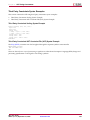
Names With Spaces in Command Line Mode
XST supports file and directory names with spaces in command line mode. Enclose file or directory names
containing spaces in double quotes: C:\my project
The command line syntax for options supporting multiple directories (-sd, -vlgincdir) has changed. Enclose
multiple directories in braces: -vlgincdir {"C:\my project" C:\temp }
In previous releases, multiple directories were included in double quotes. XST still supports this convention,
provided directory names do not contain spaces. Xilinx® recommends that you change existing scripts to the
new syntax.
Launching XST in Command Line Mode
You can launch XST in command line mode using:
•
The XST shell
•
A script file
Launching XST in Command Line Mode Using the XST Shell
Type xst to enter directly into an XST shell. Enter your commands and execute them. To run synthesis, specify a
complete command with all required options. XST does not accept a mode where you can first enter set
option_1, then set option_2, and then enter run.
Since all options are set at the same time, Xilinx® recommends that you use a script file.
Launching XST in Command Line Mode Using a Script File
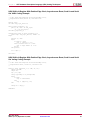
Store your commands in a separate script file and run them all at once. To execute your script file, run the
following workstation or PC command:
xst -ifn in_file_name -ofn out_file_name -intstyle {silent|ise|xflow}
The -ofn option is not mandatory. If you omit it, XST automatically generates a log file with the file extension
.srp, and all messages display on the screen. Use the following to limit the number of messages printed to
the screen:
•
The -intstyle silent option
•
The XIL_XST_HIDEMESSAGES environment variable
•
The message filter feature in ISE® Design Suite
For more information, see Reducing the Size of the XST Log File.
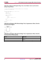
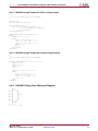
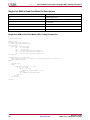
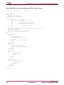
For example, assume that the following text is contained in a file foo.scr:
run
-ifn tt1.prj
-top tt1
-ifmt MIXED
-opt_mode SPEED
-opt_level 1
-ofn tt1.ngc
-p <parttype>
476
www.xilinx.com
XST User Guide
UG627 (v 11.3) September 16, 2009