1
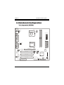
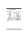
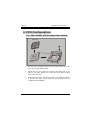
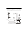
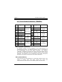
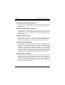
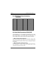
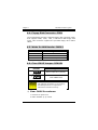
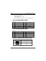
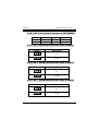
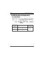
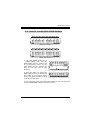
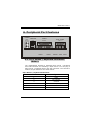
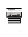
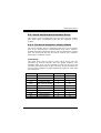
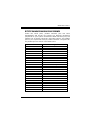
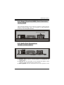
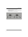
FCC Information and Copyright
This equipment has been tested and found to comply with the
limits of a Class B digital device, pursuant to Part 15 of the FCC
Rules. These limits are designed to provide reasonable protection
against harmful interference in a residential installation. This
equipment generates, uses and can radiate radio frequency
energy and, if not installed and used in accordance with the
instructions, may cause
harmful interference to radio
communications. There is no guarantee that interference will not
occur in a particular installation.
The vendor makes no representations or warranties with respect
to the contents here of and specially disclaims any implied
warranties of merchantability or fitness for any purpose. Further
the vendor reserves the right to revise this publication and to
make changes to the contents here of without obligation to notify
any party beforehand.
Duplication of this publication, in part or in whole, is not allowed
without first obtaining the vendor’s approval in writing.
The content of this user’s manual is subject to be changed without
notice and we will not be responsible for any mistakes found in
this user’s manual. All the brand and product names are
trademarks of their respective companies.
Table of Contents
Notice .............................................................................................1
Mainboard Features ...............................................................2
1. Features Introduction......................................................................... 2
1-1. Hardware............................................................................................................ 2
1-2. BIOS & Software............................................................................................ 6
1-3. Package Contents.......................................................................................... 6
2. Mainboard Configuration................................................................... 7
2-1. Layout of U8768 ............................................................................................ 7
2-2. Component Index ......................................................................................... 8
3. CPU Configuration ............................................................................... 9
3-1. CPU Socket 478 Configuration Steps:............................................... 9
3-2. CPU Fan Header: JCFAN1....................................................................... 10
3-3. System Fan Header: JSFAN1 ............................................................... 11
4. Jumpers, Headers & Connectors.................................................. 12
4-1. Front Panel Connector: JPANEL1 ....................................................... 13
4-2. ATX 20-pin Power Connector: JATXPWR1.................................... 15
4-3. Hard Disk Connectors: IDE1/IDE2.................................................... 15
4-4. Floppy Disk Connector: FDD1.............................................................. 16
4-5. Wake On LAN Header: JWOL1 ............................................................ 16
4-6. Clear CMOS Jumper: JCMOS1............................................................. 16
4-7. Front USB Header: JUSB3...................................................................... 17
4-8. Front USB Header: JUSB4...................................................................... 17
4-9. 5V / 5VSB Selection for KB: JKBV1.................................................. 17
i
Table of Contents
4-10. ATX 12V Power Connector: JATXPWR2....................................... 18
4-11. 5V / 5VSB Selection for USB: JUSBV1......................................... 18
4-12. 5V / 5VSB Selection for USB: JUSBV3......................................... 18
4-13. 5V / 5VSB Selection for USB: JUSBV4......................................... 18
5. RAM Module Configuration ............................................................. 19
5-1. DDR SDRAM................................................................................................... 19
5-2. How to install DDR DIMM Module...................................................... 20
6. Peripheral Port Features ................................................................. 21
6-1. PS/2 Mouse / Keyboard Connector: JKBMS1 ............................. 21
6-2. USB & LAN Port Connectors: JUSBLAN1 ....................................... 22
6-3. Serial and Parallel Interface Ports...................................................... 24
6-6. Audio Subsystem......................................................................................... 28
ii
Chapter 1
Motherboard Description
Notice
Introduction of system
This mainboard is designed to take advantage of the latest industry
technology to provide you with the ultimate solution in data
processing. In the tradition of its predecessors, this mainboard
continues a commitment to reliability and performance and strives
for full compliance and compatibility with industry software and
hardware standards.
U8768 Features:
1.Contains on board I/O facilities that include two serial ports, a parallel
port, a PS/2 mouse port, a PS/2 keyboard port, audio ports, USB
ports and a game port.
2.Contains on board IDE facilities for IDE devices such as hard disks
and CD-ROM Drives.
3.Supports the Intel Pentium ® 4 processor, a leading edge processor.
Complies with PC Micro-ATX form factor specifications.
4.Supports popular operating systems such as Windows NT, Windows
2000, Windows ME, Windows XP, Novell, LINUX and SCO UNIX.
1-1
Chapter 1
Motherboard Description
Mainboard Features
1. Features Introduction
1-1. Hardware
CPU:
1.Provides Socket-478.
®
2.Supports the Intel Pentium 4 processor providing the new generation power
for high-end workstations and servers.
Speed:
1.Running at 533 MHz Front Side Bus frequency.
2.Supports up to 2.53 GHz CPU core speeds.
3.The 33MHz 32 bit PCI 2.2 compliant.
4.The 66MHz AGP 2.0 compliant interface supports 1x, 2x and 4x data transfer
mode.
Chipset:
Chipset – VIA VT8753E (P4X266E)/ VT8235.
Super I/O
Chipset – ITE 8705
DRAM Memory:
1.Supports 200MHz, 266MHz DDR SDRAM devices.
2.Supports 64Mb, 128Mb, 256Mb and 512Mb technologies for x8 and 16
devices.
3.Max of 2 Double-Sided DDR SDRAM with unbuffered / Registered.
4.The largest memory capacity is 2 GB.
1-2
Chapter 1
Motherboard Description
Shadow RAM:
Motherboard is equipped with a memory controller providing shadow RAM and
support for ROM BIOS.
Green Functionality:
1.Supports Award BIOS ™ power management functionality.
2.Has a power down timer from 1 to 15 minutes.
BUS Slots:
1.Contains 1 AGP slot.
2.Contains 1 CNR slot.
3. Contains 3 32-bit PCI bus slots
Flash Memory:
1.Supports flash memory functionality.
2.Supports ESCD functionality.
Built in IDE Facilities:
1.Supports four IDE hard disk drives.
2.Supports PIO Mode 4, Master Mode, and high performance hard disk drives.
3.Supports disk transfer rates up to 133 MB/second.
4.Supports Ultra DMA 33, Ultra DMA 66, Ultra DMA 100, Ultra DMA 133 Bus
Master Modes.
5.Supports IDE interface with CD-ROM.
6.Supports high capacity hard disk drives.
7.Supports LBA mode.
1-3
Chapter 1
Motherboard Description
AC’97 Sound Codec Onboard:
1.AC-LINK protocol comfliance.
2.Compliant with AC’97 specification.
3.18-bit full duplex stereo ADC, DACs.
4.SNR>95 Bb throughmixer and DAC.
5. Full-duplex codec.
6. Earphone buffer.
7. Line in/ Rear out share jack capability.
8. Mic in/ Center and Bass out share jack capability.
9. Internal PLL built-in saving additional crystal.
10. Meet Microsoft’s ® PC2001 requirements.
11. Support 6-CH speaker mode.
I/O facilities:
1.One multi-mode Parallel Port capable of supporting the following
specifications:
Standard & Bidirection Parallel Port.
Enhanced Parallel Port (EPP).
Extended Capabilities Port (ECP).
Normal
2.Supports two serial ports, 16550 UART.
3.Supports Infrared Data Transmission using IrDA.
4.Supports PS/2 mouse and PS/2 keyboard.
5.Supports 360KB, 720KB, 1.2MB, 1.44MB, and 2.88MB floppy disk drives.
Universal Serial Bus:
Supports two back panel Universal Serial Bus Port and four front panel
Universal Serial Bus Ports.
Hardware Monitor Function:
1.Monitors CPU Fan Speed.
2.Monitors System Voltage.
1-4
Chapter 1
Motherboard Description
Dimensions (MATX form-factor):
24.5cm x 22.8cm (WxL)
1-5
Chapter 1
Motherboard Description
1-2. BIOS & Software
1.Award legal BIOS.
2.Supports APM1.2.
3.Supports USB Function.
4.Supports ACPI.
Operating System:
Offers the highest performance for MS-DOS, Windows NT, Windows 2000,
Windows ME, Windows XP, Novell, LINUX, and SCO UNIX etc.
1-3. Package Contents
1.HDD Cable.
2.FDD Cable.
3.Flash Memory Writer for BIOS Update.
4.USB Cable (Optional).
5.Rear I/O Panel for MATX Case (Optional).
6.Fully Setup Driver CD.
1-6
Chapter 1
Motherboard Description
2. Mainboard Configuration
2-1. Layout of U8768
JKBMS1
K/B
&
Mouse
1
JUSBLAN1
USB & LAN
CPU1
JKBV1
Socket 478
1
JUSBV1
C PU
JATXPWR1
PRIMARY IDE CONN.
JATXPWR2
P4X266E
Game Port
MIC
In
Line Speaker
Out
In
JPRNT1
JCOM2
SECONDARY IDE CONN.
COM2
Parallel Port
COM1
JCOM1
JGAME1
2
1
10
9
AGP SLOT
VT6103
PCI1
JAUDIO1
PCI SLOT
CMI
9739
2
1
1
PCI2
JUSB3
JUSBV3
10 2
9 1
JUSB4
BAT1
10
9
1
JUSBV4
BIOS
JCDIN1
PCI3
ITE I/O
CNR SLOT
JWOL1
1
1-7
2
1
JPANEL1
PCI SLOT
CNR1
23
VT8235
PCI SLOT
1
24
1
JCMOS1
FLOPPY DISK CONN.
Chapter 1
Motherboard Description
2-2. Component Index
Socket 478
C PU
P4X266E
VT6103
BAT1
5V/ 5VSB Selection for USB (JUSBV4)
CMI
9739
BIOS
VT8235
5V/ 5VSB Selection for USB (JUSBV3)
ITE I/O
1-8
Chapter 1
Motherboard Description
3. CPU Configuration
3-1. CPU Socket 478 Configuration Steps:
CPU Fan
CPU
1.
Pull the lever sideways away from the socket then raise the
lever up to a 90-degree angle.
2.
Locate Pin A in the socket and look for the white dot or cut
edge in the CPU. Match Pin A with the white dot/cut edge
then insert the CPU.
3.
Press the lever down. Then Put the fan on the CPU and buckle
it and put the fan’s power port into the JCFAN1, then to
complete the installation.
1-9
Chapter 1
Motherboard Description
CPU Configuration Layout
Socket 478
CPU
P4X266E
VT6103
BAT1
CMI
9739
BIOS
VT8235
ITE I/O
3-2. CPU Fan Header: JCFAN1
Pin No.
Assignment
1
Ground
2
+12V
3
Sense
1-10
Chapter 1
Motherboard Description
3-3. System Fan Header: JSFAN1
Pin No.
Assignment
1
Ground
2
+12V
3
Sense
1-11
Chapter 1
Motherboard Description
4. Jumpers, Headers & Connectors
1
JKBV1
Socket 478
1
C PU
JUSBV1
JATXPWR1
JATXPWR2
IDE1-2
P4X266E
JUSB4
JUSB3
10
9
1
BAT1
2
1
1
JUSBV4
CMI
9739
JUSBV3
VT8235
BIOS
2
1
VT6103
JPANEL1
JCMOS1
ITE I/O
1
FDD1
JWOL1
1
1-12
10
9
Chapter 1
Motherboard Description
4-1. Front Panel Connector: JPANEL1
Pin Assignment Function Pin Assignment
No.
No.
Function
1
+5V
2
Sleep Control
Sleep
3
NA
Speaker
4
Ground
Button
5
NA
Connector
6
NA
NA
7
Speaker
8
Power LED (+)
9
HDD LED (+)
Hard Drive
10 Power LED (+)
POWER
11
HDD LED (-)
LED
12 Power LED (-)
LED
13
Ground
Reset
14
Power Button
15
Reset Control
Button
16
Ground
17
NA
18
KEY
19
NA
IrDA
20
KEY
IrDA
21
VCC5
Connector
22
Ground
Connector
23
IRTX
24
IRRX
Power-on
Button
SPK (Speaker Connector)
An offboard speaker can be installed on the motherboard as a
manufacturing option. An offboard speaker can be connected to
the motherboard at the front panel connector. The speaker
(onboard or offboard) provides error beep code information during
the Power On Self-Test when the computer cannot use the video
interface. The speaker is not connected to the audio subsystem
and does not receive output from the audio subsystem.
RST (Reset Button)
This connector can be attached to a momentary SPST switch. This
switch is usually open and when closed will cause the
motherboard to reset and run the POST (Power On Self Test).
1-13
Chapter 1
Motherboard Description
POW-LED (Power LED Connector)
This connector can be attached to an LED on the front panel of a
computer case. The LED will illuminate while the computer is
powered on.
HLED (Hard Drive LED Connector)
This connector can be attached to an LED on the front panel of a
computer case. The LED will flicker during disk activity. This disk
activity only applies to those IDE drives directly attached to the
system board.
IR (Infrared Connector)
This connector is used to attach to an infrared sensing device.
After the IrDA interface is configured, connectionless data transfer
to and from portable devices such as laptops, PDAs is possible.
SLP (Sleep/Green Button)
This connector is used to conserve energy by powering down the
monitor and the hard disk when not in use. To configure this
option, you need to connect a button from the front panel to this
connector. Depressing the button will power down the monitor
and hard drives until the system is invoked by any keyboard
activity, mouse activity, modem activity or when the sleep button
is depressed again. APM (Advanced Power Management) must be
enabled in the system BIOS and the APM driver must be loaded.
ON/OFF (Power Button)
This connector can be attached to a front panel power switch. The
switch must pull the Power Button pin to ground for at least 50 ms
to signal the power supply to switch on or off. (The time required
is due to internal debounce circuitry on the system board). At
least two seconds must pass before the power supply will
recognize another on/off signal.
1-14
Chapter 1
Motherboard Description
4-2. ATX 20-pin Power Connector:
JATXPWR1
PIN
Assignment
PIN
Assignment
1
3.3V
11
3.3V
2
3.3V
12
-12V
3
Ground
13
Ground
4
5V
14
PS_ON
5
Ground
15
Ground
6
5V
16
Ground
7
Ground
17
Ground
8
PW_OK
18
-5V
9
5V_SB
19
5V
10
12V
20
5V
4-3. Hard Disk Connectors: IDE1/IDE2
This mainboard has a 32-bit Enhanced PCI IDE Controller that
provides PIO Mode 0~4, Bus Master, and Ultra DMA / 33, Ultra
DMA / 66,Ultra DMA / 100, and Ultra DMA / 133 functionality. It
has two HDD connectors IDE1 (primary) and IDE2 (secondary).
• IDE1 (Primary IDE Connector)
The first hard drive should always be connected to IDE1. IDE1
can connect a Master and a Slave drive. You must configure the
second hard drive on IDE1 to Slave mode by setting the jumper
accordingly.
• IDE2 (Secondary IDE Connector)
The IDE2 controller can also support a Master and a Slave drive.
The configuration is similar to IDE1. The second drive on this
controller must be set to slave mode.
1-15
Chapter 1
Motherboard Description
4-4. Floppy Disk Connector: FDD1
The motherboard provides a standard floppy disk connector (FDC)
that supports 360K, 720K, 1.2M, 1.44M and 2.88M floppy disk
types. This connector supports the provided floppy drive ribbon
cables.
4-5. Wake On LAN Header: JWOL1
Pin No.
Assignment
1
5V SB
2
Ground
3
Wake up
4-6. Clear CMOS Jumper: JCMOS1
JCMOS1
1
Assignment
3
1-2 Closed
1
3
2-3 Closed
Normal Operation (default)
Clear CMOS Data
The following procedures are for resetting
the BIOS password. It is important to
follow these instructions closely.
※ Clear CMOS Procedures:
1. Remove AC power line.
2. Make JCMOS1 (2-3) closed.
1-16
Chapter 1
Motherboard Description
3.
4.
5.
6.
Wait for five seconds.
Make JCMOS1 (1-2) closed.
Let AC power on.
Reset your desired password or clear the CMOS data.
4-7. Front USB Header: JUSB3
(JUSB3)
Pin
1
3
5
7
9
Assignment
+5V(fused)
USBP2USBP2+
Ground
KEY
Pin
2
4
6
8
10
Assignment
+5V(fused)
USBP3USBP3+
Ground
NC
4-8. Front USB Header: JUSB4
(JUSB4)
Pin
1
3
5
7
9
Assignment
+5V(fused)
USBP2USBP2+
Ground
KEY
Pin
2
4
6
8
10
Assignment
+5V(fused)
USBP3USBP3+
Ground
NC
4-9. 5V / 5VSB Selection for KB: JKBV1
JKBV1
1
Assignment
3
5V
1-2 Closed
1
3
5V_SB
2-3 Closed
1-17
Chapter 1
Motherboard Description
4-10. ATX 12V Power Connector: JATXPWR2
PIN
Assignment
PIN
Assignment
1
12V
3
Ground
2
12V
4
Ground
4-11. 5V / 5VSB Selection for USB: JUSBV1
JUSBV1
1
Assignment
3
5V
1-2 Closed
1
3
5V_SB
2-3 Closed
4-12. 5V / 5VSB Selection for USB: JUSBV3
JUSBV3
1
Assignment
3
5V
1-2 Closed
1
3
5V_SB
2-3 Closed
4-13. 5V / 5VSB Selection for USB: JUSBV4
JUSBV4
1
Assignment
3
5V
1-2 Closed
1
3
5V_SB
2-3 Closed
1-18
Chapter 1
Motherboard Description
5. RAM Module Configuration
5-1. DDR SDRAM
DRAM Access Time: 2.5V Unbuffered DDR SDRAM
PC1600/ PC2100 Type required.
DRAM Type: 128MB/ 256MB/ 512MB/ 1GB DIMM
Module (184 pin)
Total
Memory Size
DIMMs
with
unbuffer
(Only for reference)
DIMM Socket
Location
DDR Module
DDR 1
64MB/128MB/256MB/512MB/1GB
*1
Max is
DDR 2
64MB/128MB/256MB/512MB/1GB
2GB
*1
1-19
Total Memory
Size (MB)
Mainboard Features
5-2. How to install DDR DIMM Module
Single Sided DIMM
Double Sided DIMM
1. The DDR DIMM socket has a
“ Plastic Safety Tab”, and the
DDR DIMM memory module has
an Asymmetrical notch”, so the
DDR DIMM memory module can
only fit into the slot in one
direction.
2. Push the tabs out. Insert the
DDR DIMM memory modules into
the socket at a 90-degree angle,
then push down vertically so that
it will fit into the place.
3. The Mounting Holes and plastic tabs should fit over the edge and
hold the DDR DIMM memory modules in place.
20
Mainboard Features
6. Peripheral Port Features
JKBMS1
PS/2
Mouse
PS/2
Keyboard
JUSBLAN1
JPRNT1
LAN
USB
JAUD_GAME
Game Port
Parallel
COM1
COM2
JCOM1
JCOM2
Speaker Line In Mic
Out
In
JSPKR1 JLIN1 JMIC1
6-1. PS/2 Mouse / Keyboard Connector:
JKBMS1
The motherboard provides a standard PS/2 mouse / Keyboard
mini DIN connector for attaching a PS/2 mouse. You can plug a
PS/2 mouse / Keyboard directly into this connector. The connector
location and pin definition are shown below:
PS/2 Mouse / Keyboard Connectors
Pin
Assignment
1
Data
2
No connect
3
Ground
4
+5 V (fused)
5
Clock
6
No connect
21
Mainboard Features
6-2. USB & LAN Port Connectors: JUSBLAN1
6-2-1. USB Connectors:
USB Connector (the below one)
Pin
Assignment
1
+5 V (fused)
2
USBP1-
3
USBP1+
4
Ground
USB Connector (the above one)
Pin
Assignment
5
+5 V (fused)
6
USBP2-
7
USBP2+
8
Ground
22
Mainboard Features
6-2-2. LAN Port Connector
This connector allows you to connect to the Internet through a
Local Area Network (LAN). You can set up the connection by
entering account information provided by your ISP.
LAN Port Connector
Pin
Assignment
9
VCC3
10
TD+
11
TD-
12
RD+
13
RD-
14
NC
23
Mainboard Features
6-3. Serial and Parallel Interface Ports
This system comes equipped with two serial ports and one parallel
port. Both types of interface ports will be explained in this
chapter.
6-3-1. The Serial Interface: JCOM1/JCOM2
The serial interface port is sometimes referred to as an RS-232
port or an asynchronous communication port. Mice, printers,
modems and other peripheral devices can be connected to a serial
port. The serial port can also be used to connect your computer
with another computer system.
Connectivity
The serial ports can be used in many ways, and it may be
necessary to become familiar with the pinout diagram. The
following chart gives you the function of each pin on the 9-pin
connector and some of the 25-pin connector. This information can
be used when configuring certain software programs to work with
the serial ports.
Signal
Name
DB9 PIN
DB25 PIN
DCD
Data Carrier Detect
1
8
RX
Receive Data
2
3
TX
Transmit Data
3
2
DTR
Data Terminal Ready
4
20
GND
Signal Ground
5
7
DSR
Data Set Ready
6
6
RTS
Request to Send
7
4
CTS
Clear to Send
8
5
RI
Ring Indicator
9
22
24
Mainboard Features
6-3-2. Parallel Interface Port: JPRNT1
Unlike the serial ports, parallel interface port has been
standardized and should not present any difficulty interfacing
peripherals to your system. Sometimes called centronics port, the
parallel port is almost exclusively used with printers. The parallel
port on your system has a 25-pin, DB25 connector. The pinout for
the parallel port are shown in the table below.
Pin
1
2
3
4
5
6
7
8
9
10
11
12
13
14
15
16
17
18
19
20
21
22
23
24
25
Signal
-Strobe
Data 0
Data 1
Data 2
Data 3
Data 4
Data 5
Data 6
Data 7
-Ack
Busy
Paper Empty
+Select
-Auto FDXT
-Error
-Init
-SLCTN
Ground
Ground
Ground
Ground
Ground
Ground
Ground
Ground
25
Mainboard Features
6-4. Game (Joystick/MIDI) Port Connector:
JAUD_GAME
This connector allows you to connect a joystick or game pad for
playing computer games. Also, you may play or edit professional
music by connecting MIDI devices.
Game/Joystick/MIDI
6-5. Audio Port Connectors:
JSPKR1/JLIN1/JMIC1
Speaker Out
Line In
Mic In
1. Speaker Out is used to connect speakers or headphones for
audio output.
2. Line In can be connected to the external CD player, Tape
player or other audio devices for audio input.
3. Rear Speaker can be connected to the rear speakers while
26
Mainboard Features
four/six channel speakers mode is enabled.
4. Mic In is used to connect a microphone, which allows you to
input sounds and voices.
5. Center and Bass can be connected to center speaker and bass
while six channel speakers mode is enabled.
4 Ch annel Speakers
Speaker Out
Line In/
Mic In
Rear Speaker
6 Ch annel Speakers
Speaker Out
27
Line In/
Rear Speaker
Mic In/ Center & Bass
Mainboard Features
6-6. Audio Subsystem
Socket 478
C PU
P4X266E
2
1
10
9
VT6103
BAT1
JAUDIO1
CMI
9739
1
JCDIN1
BIOS
VT8235
ITE I/O
28
Mainboard Features
6-6-1. CD-ROM Audio-In Header: JCDIN1
Pin No.
Assignment
1
Left Channel Input
2
Ground
3
Ground
4
Right Channel Input
6-6-2. Front Panel Audio Header: JAUDIO1
Pin No.
Assignment
Pin No.
Assignment
1
Mic In
2
Ground
3
Mic Power
4
Audio Power
5
RT Line Out
6
RT Line Out
7
Reserved
8
9
LFT Line Out
10
29
LFT Line Out
06/28/2002