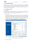
1
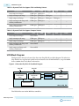
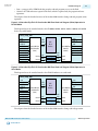
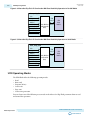
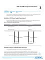
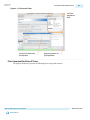
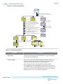
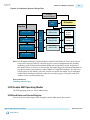
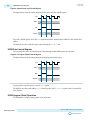
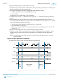
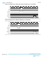
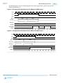
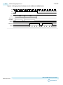
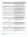
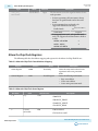
MAX 10 User Flash Memory User Guide
Subscribe
Send Feedback
UG-M10UFM
2015.05.04
101 Innovation Drive
San Jose, CA 95134
www.altera.com
TOC-2
Contents
MAX 10 User Flash Memory Overview...............................................................1-1
MAX 10 UFM Architecture and Features...........................................................2-1
UFM and CFM Array Size.......................................................................................................................... 2-1
UFM Memory Organization Map............................................................................................................. 2-1
UFM Block Diagram................................................................................................................................... 2-2
UFM Operating Modes............................................................................................................................... 2-4
MAX 10 UFM Design Considerations................................................................ 3-1
Guideline: UFM Power Supply Requirement.......................................................................................... 3-1
Guideline: Program and Read UFM with JTAG..................................................................................... 3-1
Guideline: UFM Content Initialization.................................................................................................... 3-2
Guideline: Erase Before Program.............................................................................................................. 3-2
MAX 10 UFM Implementation Guides.............................................................. 4-1
Altera On-Chip Flash IP Core....................................................................................................................4-1
Introduction to Altera IP Cores..................................................................................................... 4-1
Specifying IP Core Parameters and Options................................................................................4-1
Files Generated for Altera IP Cores...............................................................................................4-3
Simulating Altera IP Cores in other EDA Tools..........................................................................4-6
UFM Avalon-MM Operating Modes........................................................................................................4-7
UFM Read Status and Control Register........................................................................................4-7
UFM Write Control Register..........................................................................................................4-8
UFM Program (Write) Operation................................................................................................. 4-8
UFM Sector Erase Operation....................................................................................................... 4-10
UFM Page Erase Operation..........................................................................................................4-10
UFM Read Operation....................................................................................................................4-11
UFM Burst Read Operation......................................................................................................... 4-13
Altera On-Chip Flash IP Core References.......................................................... 5-1
Altera On-Chip Flash Parameters............................................................................................................. 5-1
Altera On-Chip Flash Signals.....................................................................................................................5-2
Altera On-Chip Flash Registers................................................................................................................. 5-4
Additional Information for MAX 10 UFM User Guide ................................... A-1
Document Revision History for Content MAX 10 User Flash Memory User Guide....................... A-1
Altera Corporation
1
MAX 10 User Flash Memory Overview
2015.05.04
UG-M10UFM
Subscribe
Send Feedback
Altera MAX® 10 FPGAs offer a user flash memory (UFM) block that stores non-volatile information.
The UFM provides an ideal storage solution that you can access using the Avalon Memory Mapped
(Avalon-MM) slave interface to UFM.
The UFM block also offers the following features.
Features
Endurance
Capacity
Counts up to 10,000 program/erase cycles
Data retention (after 10,000 program/ • 20 years at 85 ºC
erase cycles)
• 10 years at 100 ºC
Maximum operating frequency
• Serial interface: 7.25 MHz
• Parallel interface: 116 MHz
Data length
Stores data of up to 32 bits length in parallel
© 2015 Altera Corporation. All rights reserved. ALTERA, ARRIA, CYCLONE, ENPIRION, MAX, MEGACORE, NIOS, QUARTUS and STRATIX words and logos are
trademarks of Altera Corporation and registered in the U.S. Patent and Trademark Office and in other countries. All other words and logos identified as
trademarks or service marks are the property of their respective holders as described at www.altera.com/common/legal.html. Altera warrants performance
of its semiconductor products to current specifications in accordance with Altera's standard warranty, but reserves the right to make changes to any
products and services at any time without notice. Altera assumes no responsibility or liability arising out of the application or use of any information,
product, or service described herein except as expressly agreed to in writing by Altera. Altera customers are advised to obtain the latest version of device
specifications before relying on any published information and before placing orders for products or services.
www.altera.com
101 Innovation Drive, San Jose, CA 95134
ISO
9001:2008
Registered
MAX 10 UFM Architecture and Features
2
2015.05.04
UG-M10UFM
Subscribe
Send Feedback
The UFM architecture of MAX 10 devices is a combination of soft and hard IPs. You can only access the
UFM using the Altera On-Chip Flash IP core in the Quartus II software.
UFM and CFM Array Size
Each array is organized as various sectors. You can erase each page or sector independently. The Altera
On-Chip Flash IP core also gives you access to configuration flash memory (CFM) based on your
specification in the parameter editor.
Table 2-1: UFM and CFM Array Size
This table lists the dimensions of the UFM and CFM arrays.
Device
Pages per Sector
UFM1
UFM0
CFM2
CFM1
CFM0
Page Size
(Kb)
Total User Flash
Memory Size (Kb)
(1)
Total Configuration
Memory Size (Kb)
10M02
3
3
0
0
34
16
96
544
10M04
0
8
41
29
70
16
1248
2240
10M08
8
8
41
29
70
16
1376
2240
10M16
4
4
38
28
66
32
2368
4224
10M25
4
4
52
40
92
32
3200
5888
10M40
4
4
48
36
84
64
5888
10752
10M50
4
4
48
36
84
64
5888
10752
UFM Memory Organization Map
The address scheme changes based on the configuration mode you specify in the Altera On-Chip Flash
parameter editor.
The following tables show the dynamic UFM and CFM support based on different configuration mode
and MAX10 FPGA variant.
(1)
The maximum possible value, which is dependent on the mode you select.
© 2015 Altera Corporation. All rights reserved. ALTERA, ARRIA, CYCLONE, ENPIRION, MAX, MEGACORE, NIOS, QUARTUS and STRATIX words and logos are
trademarks of Altera Corporation and registered in the U.S. Patent and Trademark Office and in other countries. All other words and logos identified as
trademarks or service marks are the property of their respective holders as described at www.altera.com/common/legal.html. Altera warrants performance
of its semiconductor products to current specifications in accordance with Altera's standard warranty, but reserves the right to make changes to any
products and services at any time without notice. Altera assumes no responsibility or liability arising out of the application or use of any information,
product, or service described herein except as expressly agreed to in writing by Altera. Altera customers are advised to obtain the latest version of device
specifications before relying on any published information and before placing orders for products or services.
www.altera.com
101 Innovation Drive, San Jose, CA 95134
ISO
9001:2008
Registered
2-2
UG-M10UFM
2015.05.04
UFM Block Diagram
Table 2-2: Dynamic Flash Size Support: Flash and Analog Variants
Configuration
UFM1
UFM0
CFM2
CFM1
CFM0
—
—
—
Dual compressed images
UFM space UFM space
Single uncompressed image
UFM space UFM space UFM space
Single compressed image
UFM space UFM space UFM space UFM space
Single uncompressed image with
memory initialization
UFM space UFM space
Single compressed image with
memory initialization
UFM space UFM space
—
—
—
—
—
—
—
CFM2
CFM1
CFM0
Table 2-3: Dynamic Flash Size Support: Compact Variant
Configuration
UFM1
UFM0
Dual compressed images
Not available
Single uncompressed image
UFM space UFM space
—
—
—
Single compressed image
UFM space UFM space
—
—
—
Single uncompressed image with
memory initialization
Not available
Single compressed image with
memory initialization
Not available
UFM Block Diagram
This figure shows the top level view of the Altera On-Chip Flash IP core block diagram. The Altera OnChip Flash IP core supports both parallel and serial interfaces for all MAX 10 FPGAs, except for 10M02
devices. 10M02 devices only allow serial interface.
Figure 2-1: Altera On-Chip Flash IP Core Block Diagram
Avalon-MM
Avalon-MM
Avalon-MM Slave
Parallel Controller
(Data)
Parallel
Avalon-MM Slave
Serial Controller
(Data)
Avalon-MM
Control Register
Status Register
Avalon-MM Slave Controller
(Control)
Serial
UFM Block Interface
altera_onchip_flash
This IP block has two Avalon-MM slave controllers:
Altera Corporation
MAX 10 UFM Architecture and Features
Send Feedback
UG-M10UFM
2015.05.04
UFM Block Diagram
2-3
• Data—a wrapper of the UFM block that provides read and program accesses to the flash.
• Control—the CSR and status register for the flash, which is required only for program and erase
operations.
These figures show the detailed overview of the Avalon-MM interface during read and program (write)
operation.
Figure 2-2: Altera On-Chip Flash IP Core Avalon-MM Slave Read and Program (Write) Operation in
Parallel Mode
This diagram shows the standard interface for all 10M04, 10M08, 10M16, 10M25, 10M40, and 10M50
devices in parallel mode.
altera_onchip_flash
clock
reset_n
addr[x:0]
read
readdata[31:0]
write
writedata[31:0]
waitrequest
readdatavalid
burstcount[x:0]
UFM
Block I/F
Avalon-MM Slave Parallel
Parallel Controller
(Data)
clock
reset_n
UFM
Block
Interface
internal read
Control Register
internal write
Status Register
Avalon-MM Slave
Controller
(Control)
read/
write
read
addr
read
readdata[31:0]
write
writedata[31:0]
external
external
Figure 2-3: Altera On-Chip Flash IP Core Avalon-MM Slave Read and Program (Write) Operation in
Serial Mode
This diagram shows the standard interface for all MAX 10 devices in serial mode.
altera_onchip_flash
clock
reset_n
addr[x:0]
read
readdata
write
writedata
waitrequest
readdatavalid
burstcount[x:0]
UFM
Block I/F
Avalon-MM Slave
Serial Controller
(Data)
Serial
clock
reset_n
UFM
Block
Interface
internal read
Control Register
internal write
Status Register
Avalon-MM Slave
Controller
(Control)
read/
write
read
addr
read
readdata[31:0]
write
writedata[31:0]
external
external
These figures show the detailed overview of the Avalon-MM interface during read only operation.
MAX 10 UFM Architecture and Features
Send Feedback
Altera Corporation
2-4
UG-M10UFM
2015.05.04
UFM Operating Modes
Figure 2-4: Altera On-Chip Flash IP Core Avalon-MM Slave Read Only Operation in Parallel Mode
altera_onchip_flash
clock
reset_n
addr[x:0]
read
readdata[31:0]
waitrequest
readdatavalid
burstcount[x:0]
UFM
Block I/F
Avalon-MM Slave Parallel
Parallel Controller
(Data)
UFM
Block
Interface
Figure 2-5: Altera On-Chip Flash IP Core Avalon-MM Slave Read Only Operation in Serial Mode
altera_onchip_flash
clock
reset_n
addr[x:0]
read
readdata
waitrequest
readdatavalid
burstcount[x:0]
UFM
Block I/F
Avalon-MM Slave
Serial Controller
(Data)
Serial
UFM
Block
Interface
UFM Operating Modes
The UFM block offers the following operating modes:
•
•
•
•
•
•
Read
Burst read
Program (Write)
Sector erase
Page erase
Sector write protection
You can choose one of the following access modes in the Altera On-Chip Flash parameter editor to read
and control the operations.
Altera Corporation
MAX 10 UFM Architecture and Features
Send Feedback
UG-M10UFM
2015.05.04
UFM Operating Modes
2-5
• Read and program mode—this mode allows both data and control slave interface. This mode is
applicable for both UFM and CFM sectors.
• Read only mode—this mode allows only data slave interface, and restricted to only read operations.
This mode is applicable for both UFM and CFM sectors.
• Hidden—this mode does not allow any read or program (write) operations. This mode is applicable
only for CFM sectors.
The following table shows the comparison between parallel and serial modes.
Table 2-4: Comparison between Parallel Mode and Serial Mode
Feature
Parallel Mode
Serial Mode
Avalon-MM Data Interface
Parallel mode with 32-bit
data bus
Serial mode with 32 bits based burst
count
Access Mode
• Read and program
• Read only
• Hidden
• Read and program
• Read only
• Hidden
Read Mode
• Incrementing burst
read
• Wrapping burst read
Incrementing burst read only
Program (Write) Operation
Single 32-bit parallel
program operation
Single 32-bit serial program
operation
MAX 10 UFM Architecture and Features
Send Feedback
Altera Corporation
MAX 10 UFM Design Considerations
3
2015.05.04
UG-M10UFM
Subscribe
Send Feedback
There are several considerations that require your attention to ensure the success of your designs. Unless
noted otherwise, these design guidelines apply to all variants of this device family.
Guideline: UFM Power Supply Requirement
During UFM and CFM operations, make sure to follow the maximum slew rate requirement for power
supply ramp down. This setting prevents device damage in case of power loss.
Table 3-1: Maximum Slew Rate Requirement
Device
Maximum Slew Rate
Single-supply device
0.073V/µs
Multi-supply device
0.023V/µs
3.3V
2.5V
0V
0V
<0.073V/µs
<0.023V/µs
Single-Supply Device
Multi-Supply Device
Guideline: Program and Read UFM with JTAG
You can program UFM using JTAG interface version IEEE Standard 1149.1.
© 2015 Altera Corporation. All rights reserved. ALTERA, ARRIA, CYCLONE, ENPIRION, MAX, MEGACORE, NIOS, QUARTUS and STRATIX words and logos are
trademarks of Altera Corporation and registered in the U.S. Patent and Trademark Office and in other countries. All other words and logos identified as
trademarks or service marks are the property of their respective holders as described at www.altera.com/common/legal.html. Altera warrants performance
of its semiconductor products to current specifications in accordance with Altera's standard warranty, but reserves the right to make changes to any
products and services at any time without notice. Altera assumes no responsibility or liability arising out of the application or use of any information,
product, or service described herein except as expressly agreed to in writing by Altera. Altera customers are advised to obtain the latest version of device
specifications before relying on any published information and before placing orders for products or services.
www.altera.com
101 Innovation Drive, San Jose, CA 95134
ISO
9001:2008
Registered
3-2
UG-M10UFM
2015.05.04
Guideline: UFM Content Initialization
The JTAG interface supports Jam™ Standard Test and Programming Language (STAPL) Format File
(.jam), Programmer Object File (.pof), and JAM Byte Code File (.jbc).
Guideline: UFM Content Initialization
You can initialize the UFM content using Altera software.
The initial memory content supports Memory Initialization File (.mif), and Hexadecimal (Intel-Format)
File (.hex).
You can initialize the UFM content using either one of the following ways:
• Set the initial memory content through the Altera On-Chip Flash IP core.
• Set the initial memory content through the Convert Programming File tool in the Quartus II software
when you convert .sof to .pof.
Guideline: Erase Before Program
Make sure to erase the flash location before you perform a program (write) operation.
Altera Corporation
MAX 10 UFM Design Considerations
Send Feedback
MAX 10 UFM Implementation Guides
4
2015.05.04
UG-M10UFM
Subscribe
Send Feedback
Altera On-Chip Flash IP Core
The Altera IP core design flow helps you get started with any Altera IP core.
Introduction to Altera IP Cores
Altera® and strategic IP partners offer a broad portfolio of off-the-shelf, configurable IP cores optimized
for Altera devices. The Quartus® II software installation includes the Altera IP library. You can integrate
optimized and verified Altera IP cores into your design to shorten design cycles and maximize
performance. You can evaluate any Altera IP core in simulation and compilation in the Quartus II
software. The Quartus II software also supports integration of IP cores from other sources. Use the IP
Catalog to efficiently parameterize and generate synthesis and simulation files for a custom IP variation.
The Altera IP library includes the following categories of IP cores:
•
•
•
•
•
•
Basic functions
DSP functions
Interface protocols
Low power functions
Memory interfaces and controllers
Processors and peripherals
Note: The IP Catalog (Tools > IP Catalog) and parameter editor replace the MegaWizard Plug-In
Manager for IP selection and parameterization, beginning in Quartus II software version 14.0. Use
the IP Catalog and parameter editor to locate and paramaterize Altera and other supported IP
cores.
™
Related Information
• IP User Guide Documentation
• Altera IP Release Notes
Specifying IP Core Parameters and Options
You can quickly configure a custom IP variation in the parameter editor. Use the following steps to
specify IP core options and parameters in the parameter editor. Refer to Specifying IP Core Parameters
and Options (Legacy Parameter Editors) for configuration of IP cores using the legacy parameter editor.
© 2015 Altera Corporation. All rights reserved. ALTERA, ARRIA, CYCLONE, ENPIRION, MAX, MEGACORE, NIOS, QUARTUS and STRATIX words and logos are
trademarks of Altera Corporation and registered in the U.S. Patent and Trademark Office and in other countries. All other words and logos identified as
trademarks or service marks are the property of their respective holders as described at www.altera.com/common/legal.html. Altera warrants performance
of its semiconductor products to current specifications in accordance with Altera's standard warranty, but reserves the right to make changes to any
products and services at any time without notice. Altera assumes no responsibility or liability arising out of the application or use of any information,
product, or service described herein except as expressly agreed to in writing by Altera. Altera customers are advised to obtain the latest version of device
specifications before relying on any published information and before placing orders for products or services.
www.altera.com
101 Innovation Drive, San Jose, CA 95134
ISO
9001:2008
Registered
4-2
Specifying IP Core Parameters and Options
UG-M10UFM
2015.05.04
1. In the IP Catalog (Tools > IP Catalog), locate and double-click the name of the IP core to customize.
The parameter editor appears.
2. Specify a top-level name for your custom IP variation. The parameter editor saves the IP variation
settings in a file named <your_ip>.qsys. Click OK.
3. Specify the parameters and options for your IP variation in the parameter editor, including one or
more of the following. Refer to your IP core user guide for information about specific IP core
parameters.
4.
5.
6.
7.
8.
9.
Altera Corporation
• Optionally select preset parameter values if provided for your IP core. Presets specify initial
parameter values for specific applications.
• Specify parameters defining the IP core functionality, port configurations, and device-specific
features.
• Specify options for processing the IP core files in other EDA tools.
Click Generate HDL, the Generation dialog box appears.
Specify output file generation options, and then click Generate. The IP variation files generate
according to your specifications.
To generate a simulation testbench, click Generate > Generate Testbench System.
To generate an HDL instantiation template that you can copy and paste into your text editor, click
Generate > HDL Example.
Click Finish. The parameter editor adds the top-level .qsys file to the current project automatically. If
you are prompted to manually add the .qsys file to the project, click Project > Add/Remove Files in
Project to add the file.
After generating and instantiating your IP variation, make appropriate pin assignments to connect
ports.
MAX 10 UFM Implementation Guides
Send Feedback
UG-M10UFM
2015.05.04
Files Generated for Altera IP Cores
4-3
Figure 4-1: IP Parameter Editor
View IP port
and parameter
details
Specify your IP variation name
and target device
Apply preset parameters for
specific applications
Files Generated for Altera IP Cores
The Quartus II software generates the following IP core output file structure:
MAX 10 UFM Implementation Guides
Send Feedback
Altera Corporation
4-4
UG-M10UFM
2015.05.04
Files Generated for Altera IP Cores
Figure 4-2: IP Core Generated Files
<project directory>
<your_ip>.qsys - System or IP integration file
<your_ip>.sopcinfo - Software tool-chain integration file
<your_ip>
<your_ip> n
<testbench>_tb
IP variation files
IP variation files
testbench system
<your_ip>_tb.qsys
Testbench system file
<your_ip>.cmp - VHDL component declaration file
<your_ip>_bb.v - Verilog HDL black box EDA synthesis file
<your_ip>_inst.v or .vhd - Sample instantiation template
<your_ip>.ppf - XML I/O pin information file
<testbench>_tb
testbench files
<your_ip>.qip - Lists IP synthesis files
<your_testbench>_tb.csv
<your_ip>.sip - Contains assingments for IP simulation files
<your_testbench>_tb.spd
<your_ip>_generation.rpt - IP generation report
<your_ip>.debuginfo - Contains post-generation information
<your_ip>.html - Connection and memory map data
sim
simulation files
<your_ip>.bsf - Block symbol schematic
<your_ip>.spd - Combines simulation scripts for multiple cores
<EDA tool setup
scripts>
sim
synth
Simulation files
IP synthesis files
<your_ip>.v or .vhd
Top-level simulation file
<EDA tool name>
Simulator scripts
<simulator_setup_scripts>
<ip subcores> n
Subcore libraries
<your_ip>.v or .vhd
Top-level IP synthesis file
synth
Subcore
synthesis files
sim
Subcore
Simulation files
<HDL files>
<HDL files>
Table 4-1: IP Core Generated Files
File Name
Description
<my_ip>.qsys
The Qsys system or top-level IP variation file. <my_ip> is the name
that you give your IP variation.
<system>.sopcinfo
Describes the connections and IP component parameterizations in
your Qsys system. You can parse its contents to get requirements
when you develop software drivers for IP components.
Downstream tools such as the Nios II tool chain use this file.
The .sopcinfo file and the system.h file generated for the Nios II tool
chain include address map information for each slave relative to each
master that accesses the slave. Different masters may have a different
address map to access a particular slave component.
Altera Corporation
MAX 10 UFM Implementation Guides
Send Feedback
UG-M10UFM
2015.05.04
Files Generated for Altera IP Cores
File Name
4-5
Description
<my_ip>.cmp
The VHDL Component Declaration (.cmp) file is a text file that
contains local generic and port definitions that you can use in VHDL
design files.
<my_ip>.html
A report that contains connection information, a memory map
showing the address of each slave with respect to each master to
which it is connected, and parameter assignments.
<my_ip>_generation.rpt
IP or Qsys generation log file. A summary of the messages during IP
generation.
<my_ip>.debuginfo
Contains post-generation information. Used to pass System Console
and Bus Analyzer Toolkit information about the Qsys interconnect.
The Bus Analysis Toolkit uses this file to identify debug components
in the Qsys interconnect.
<my_ip>.qip
Contains all the required information about the IP component to
integrate and compile the IP component in the Quartus II software.
<my_ip>.csv
Contains information about the upgrade status of the IP component.
<my_ip>.bsf
A Block Symbol File (.bsf) representation of the IP variation for use
in Quartus II Block Diagram Files (.bdf).
<my_ip>.spd
Required input file for ip-make-simscript to generate simulation
scripts for supported simulators. The .spd file contains a list of files
generated for simulation, along with information about memories
that you can initialize.
<my_ip>.ppf
The Pin Planner File (.ppf) stores the port and node assignments for
IP components created for use with the Pin Planner.
<my_ip>_bb.v
You can use the Verilog black-box (_bb.v) file as an empty module
declaration for use as a black box.
<my_ip>.sip
Contains information required for NativeLink simulation of IP
components. You must add the .sip file to your Quartus project.
<my_ip>_inst.v or _inst.vhd
HDL example instantiation template. You can copy and paste the
contents of this file into your HDL file to instantiate the IP variation.
<my_ip>.regmap
If the IP contains register information, the .regmap file generates.
The .regmap file describes the register map information of master
and slave interfaces. This file complements the .sopcinfo file by
providing more detailed register information about the system. This
enables register display views and user customizable statistics in
System Console.
MAX 10 UFM Implementation Guides
Send Feedback
Altera Corporation
4-6
UG-M10UFM
2015.05.04
Simulating Altera IP Cores in other EDA Tools
File Name
<my_ip>.svd
Description
Allows HPS System Debug tools to view the register maps of
peripherals connected to HPS within a Qsys system.
During synthesis, the .svd files for slave interfaces visible to System
Console masters are stored in the .sof file in the debug section.
System Console reads this section, which Qsys can query for register
map information. For system slaves, Qsys can access the registers by
name.
<my_ip>.v
or
HDL files that instantiate each submodule or child IP core for
synthesis or simulation.
<my_ip>.vhd
mentor/
Contains a ModelSim® script msim_setup.tcl to set up and run a
simulation.
aldec/
Contains a Riviera-PRO script rivierapro_setup.tcl to setup and run a
simulation.
/synopsys/vcs
Contains a shell script vcs_setup.sh to set up and run a VCS®
simulation.
/synopsys/vcsmx
Contains a shell script vcsmx_setup.sh and synopsys_ sim.setup file to
set up and run a VCS MX® simulation.
/cadence
Contains a shell script ncsim_setup.sh and other setup files to set up
and run an NCSIM simulation.
/submodules
Contains HDL files for the IP core submodule.
<child IP cores>/
For each generated child IP core directory, Qsys generates /synth and /
sim sub-directories.
Simulating Altera IP Cores in other EDA Tools
The Quartus II software supports RTL and gate-level design simulation of Altera IP cores in supported
EDA simulators. Simulation involves setting up your simulator working environment, compiling
simulation model libraries, and running your simulation.
You can use the functional simulation model and the testbench or example design generated with your IP
core for simulation. The functional simulation model and testbench files are generated in a project
subdirectory. This directory may also include scripts to compile and run the testbench. For a complete list
of models or libraries required to simulate your IP core, refer to the scripts generated with the testbench.
You can use the Quartus II NativeLink feature to automatically generate simulation files and scripts.
NativeLink launches your preferred simulator from within the Quartus II software.
Altera Corporation
MAX 10 UFM Implementation Guides
Send Feedback
UG-M10UFM
2015.05.04
UFM Avalon-MM Operating Modes
4-7
Figure 4-3: Simulation in Quartus II Design Flow
Design Entry
(HDL, Qsys, DSP Builder)
Altera Simulation
Models
Quartus II
Design Flow
Gate-Level Simulation
Analysis & Synthesis
Fitter
(place-and-route)
RTL Simulation
Post-synthesis functional
simulation netlist
Post-synthesis
functional
simulation
Post-fit functional
simulation netlist
Post-fit functional
simulation
Post-fit timing
simulation netlist
(Optional)
Post-fit
Post-fit timing
timing
simulation
simulation
(3)
EDA
Netlist
Writer
TimeQuest Timing Analyzer
Device Programmer
Note: Post-fit timing simulation is supported only for Stratix IV and Cyclone IV devices in the current
version of the Quartus II software. Altera IP supports a variety of simulation models, including
simulation-specific IP functional simulation models and encrypted RTL models, and plain text
RTL models. These are all cycle-accurate models. The models support fast functional simulation of
your IP core instance using industry-standard VHDL or Verilog HDL simulators. For some cores,
only the plain text RTL model is generated, and you can simulate that model. Use the simulation
models only for simulation and not for synthesis or any other purposes. Using these models for
synthesis creates a nonfunctional design.
Related Information
Simulating Altera Designs
UFM Avalon-MM Operating Modes
The UFM operating modes use Avalon-MM interface.
UFM Read Status and Control Register
You can access the control register value through the Avalon-MM control slave interface.
MAX 10 UFM Implementation Guides
Send Feedback
Altera Corporation
4-8
UG-M10UFM
2015.05.04
UFM Write Control Register
Figure 4-4: Read Status and Control Register
The figure below shows the timing diagram for the read status and control register.
clock
address
addr
read
readdata
value
To use the control register, assert the read signal and send the control register address to the control slave
address.
The flash IP core then sends the register value through the readdata bus.
UFM Write Control Register
You can program (write) the control register value through Avalon-MM control slave interface.
Figure 4-5: Program (Write) Control Register
The figure below shows the timing diagram for the program control register.
clock
address
addr
write
writedata
value
To program the control register, assert the write signal.
The flash IP core then sends address 0×01 (control register) and writedata (register value) to control the
slave interface.
UFM Program (Write) Operation
The UFM offers a single 32-bit program (write) operation.
Altera Corporation
MAX 10 UFM Implementation Guides
Send Feedback
UG-M10UFM
2015.05.04
UFM Program (Write) Operation
4-9
To perform a UFM program operation, follow these steps:
1. Disable the write protection mode. Write 0 into the write protection register for the sector of the given
data through the Avalon-MM control interface.
2. Program the following data into flash through the Avalon-MM data interface.
• Address: legal address (from Avalon-MM address map)
• Data: user data
Set burstcount to 1 (parallel mode) or 32 (serial mode).
3. The flash IP core sets the busy field in the status register to 2'b10 when the program operation is in
progress.
4. If the operation goes well, the flash IP core sets the write successful field in the status register to 1'b1
or write successful. The flash IP core sets the write successful field in the status register to 1'b0 (failed)
if one of the following conditions takes place:
• The burst count is not equal to 1 (parallel mode) or 32 (serial mode).
• The given address is out of range.
• The sector protection mode or write protection mode of the corresponding sector is not clear (the
value is not 1'b0).
5. Repeat the earlier steps if you want to perform another program operation.
6. You have to enable back the write protection mode when the program operation completes. Write 1
into the write protection register for the corresponding sector through the Avalon-MM control
interface.
Note: Check the status register after each write to make sure the program operation is successful
(write successful).
Figure 4-6: Program Operation in Parallel Mode
The figure below shows the write data timing diagram in parallel mode.
clock
address
addr
write
burstcount
1
writedata
data
waitrequest
Write
address
to UFM
MAX 10 UFM Implementation Guides
Send Feedback
UFM Programming
Max 305 µs
UFM Reset
Max 250 µs
Altera Corporation
4-10
UG-M10UFM
2015.05.04
UFM Sector Erase Operation
Figure 4-7: Program Operation in Serial Mode
The figure below shows the write data timing diagram in serial mode.
clock
address
addr
write
burstcount
32
writedata
31
30 29 28 27 26 25
6 5 4 32 1
waitrequest
Write address to UFM
Serial Write 32 bits Data
to UFM (32 Cycles)
UFM Sector Erase Operation
The sector erase operation allows the UFM to erase by sectors.
To perform a UFM sector erase operation, follow these steps:
1. Disable the write protection mode. Write 0 into the write protection register for the sector through the
Avalon-MM control interface.
2. Write the appropriate bits into the control register to select the sector erase location. The flash IP core
stores the sector erase address and initiates the sector erase operation.
Note: The IP core only accepts the sector erase address when it is in IDLE state;busy field at status
register is2'b00. If the IP core is busy, it will ignore the sector erase address.
3. The flash IP core sets the busy field in the status register to 2'b01 when the erase operation is in
progress.
4. The flash IP core then asserts the waitrequest signal if there are any new incoming read or write
commands from the data interface.
5. The flash IP core erases the sector. It stores the physical flash erase result in the erase successful field in
the status register when the sector erase operation completes.
Note: The maximum erase time is 350 ms.
6. The flash IP core sets the erase successful field in the status register to 1'b0 (failed) if one of the
following conditions takes place:
• You send an illegal sector number.
• The sector protection mode or write protection mode of the corresponding sector is not clear (the
value is not 1'b0)
7. Repeat the earlier steps if you want to perform another sector erase operation.
8. You have to enable back the write protection mode when the sector erase operation completes. Write 1
into the write protection register for the corresponding sector through the Avalon-MM control
interface.
Note: Check the status register after each erase to make sure the erase operation is successful (erase
successful).
UFM Page Erase Operation
The page erase operation allows the UFM to erase by pages.
Altera Corporation
MAX 10 UFM Implementation Guides
Send Feedback
UG-M10UFM
2015.05.04
UFM Read Operation
4-11
To perform a UFM page erase operation, follow these steps:
1. Disable the write protection mode. Write 0 into the write protection register for the sector through the
Avalon-MM control interface.
2. Write the appropriate bits into the control register to select the page erase location. The flash IP core
stores the page erase address and initiates the page erase operation.
Note: The IP core only accepts the page erase address when the IP is in IDLE state; busy field at status
register is2'b00. If the IP core is busy, it will ignore the page erase address.
3. The flash IP core sets the busy field in the status register to 2'b01 when the erase operation is in
progress.
4. The flash IP core then asserts the waitrequest signal if there are any new incoming read or write
commands from the data interface.
5. The flash IP core erases the page. It stores the physical flash erase result in the erase successful field in
the status register when the page erase operation completes.
Note: The maximum erase time is 350 ms.
6. The flash IP core sets the erase successful field in the status register to 1b'0 (failed) if you send an
illegal address.
7. Repeat the earlier steps if you want to perform another page erase operation.
8. You have to enable back the write protection mode when the page erase operation completes. Write 1
into the write protection register for the corresponding page through the Avalon-MM control
interface.
Note: Check the status register after each erase to make sure the erase operation is successful (erase
successful).
UFM Read Operation
The UFM offers a single 32-bit read operation.
To perform a read operation, the address register must be loaded with the reference address where the
data is or is going to be located in the UFM.
To perform a UFM read operation, follow these steps:
1.
2.
3.
4.
5.
Assert the read signal to send the legal data address to the data slave interface.
Set the burstcount to 1 (parallel mode) or 32 (serial mode).
The flash IP core asserts the waitrequest signal when it is busy.
The flash IP core asserts the readdatavalid signal and sends the data through the readdata bus.
The flash IP core sets the busy field in the status register to 2'b11 when the read operation is in
progress.
6. If the operation goes well, the flash IP core sets the read successful field in the status register to 1'b1 or
read successful. It sets the read successful field in the status register to 1'b0 (failed) and returns empty
flash if you try to read from an illegal address or protected sector.
The following figures show the timing diagrams for the read operations for the different MAX 10 devices
in parallel and serial modes.
MAX 10 UFM Implementation Guides
Send Feedback
Altera Corporation
4-12
UG-M10UFM
2015.05.04
UFM Read Operation
Figure 4-8: Read Operation for 10M04, 10M08, 10M16 and 10M25 Devices in Parallel Mode
clock
read
write
address
addr
burstcount
1
waitrequest
writedata
readdatavalid
readdata
data0
Figure 4-9: Read Operation for 10M40 and 10M50 Devices in Parallel Mode
clock
read
write
address
burstcount
addr
1
waitrequest
writedata
readdatavalid
readdata
Altera Corporation
data0
MAX 10 UFM Implementation Guides
Send Feedback
UG-M10UFM
2015.05.04
UFM Burst Read Operation
4-13
Figure 4-10: Read Operation for MAX 10 Devices in Serial Mode
clock
read
write
address
addr
burstcount
32
waitrequest
writedata
readdatavalid
readdata
31 30 29 28 27 26
5 4 3 2 1 0
UFM Burst Read Operation
The burst read operation is a streaming 32-bit read operation.
The burst read operation offers the following modes:
• Data incrementing burst read—allows a maximum of 128 burst counts.
• Data wrapping burst read—has fixed burst counts of 2 (10M04/08) and 4 (10M16/25/40/50)
To perform a UFM burst read operation, follow these steps:
1. Assert the read signal and send the legal burstcount and legal data addresses to the data interface.
2. The flash IP core asserts the waitrequest signal when it is busy.
3. The flash IP core then asserts the readdatavalid signal and sends the data through the readdata bus.
Note: For data wrapping burst read operation, if the address reaches the end of the flash, it wraps back
to the beginning of the flash and continues reading.
4. The flash IP core sets the busy field in the status register to 2'b11 or busy_read when the read
operation is in progress.
5. If the operation goes well, the flash IP core sets the read successful field in the status register to 1'b1 or
read successful. It sets the read successful field in the status register to 1'b0 (failed) and changes all
empty flash to 1 if you try to read from an illegal address or protected sector.
UFM Data Incrementing Burst Read
The following figures show the timing diagrams for the data incrementing burst read operations for the
different MAX 10 devices.
MAX 10 UFM Implementation Guides
Send Feedback
Altera Corporation
4-14
UG-M10UFM
2015.05.04
UFM Data Incrementing Burst Read
Figure 4-11: Incrementing Burst Read Operation for 10M04 and 10M08 Devices in Parallel Mode
clock
read
write
address
burstcount
addr
8
waitrequest
writedata
readdatavalid
readdata
data0 data1
data2 data3
data4 data5
data6 data7
Figure 4-12: Incrementing Burst Read Operation for 10M16 and 10M25 Devices in Parallel Mode
clock
read
write
address
burstcount
addr
addr
6
2
waitrequest
writedata
readdatavalid
readdata
Altera Corporation
data1 data2 data3 data4 data5 data6
data7
data8
MAX 10 UFM Implementation Guides
Send Feedback
UG-M10UFM
2015.05.04
4-15
UFM Data Incrementing Burst Read
Figure 4-13: Incrementing Burst Read Operation for 10M50 Devices in Parallel Mode
clock
read
write
addr
address
burstcount
8
waitrequest
writedata
readdatavalid
readdata
data0 data1 data2 data3
data4 data5 data6 data7
Figure 4-14: Unaligned Address Incrementing Burst Read Operation for 10M50 Devices in Parallel
Mode
clock
read
write
address
burstcount
addr
7
waitrequest
writedata
readdatavalid
readdata
MAX 10 UFM Implementation Guides
Send Feedback
data0
data1
data2
data3
data4
data5
data6
Altera Corporation
4-16
UG-M10UFM
2015.05.04
UFM Data Wrapping Burst Read
Figure 4-15: Incrementing Burst Read Operation for MAX 10 Devices in Serial Mode
clock
read
write
address
addr
burstcount
64
waitrequest
writedata
readdatavalid
readdata
63 62 61 60 59 58
31 30 29 28 27 26
UFM Data Wrapping Burst Read
The UFM IP supports data wrapping when it receives an unaligned address.
Note: Wrapping burst read is available only for parallel interface.
Table 4-2: Data Wrapping Support for MAX 10 Devices
Device
10M04, or 10M08
Data Register
Length
32
Flash IP Data
Bus Width
64
Fixed Supported
Burst Count
2
Data Wrapping
The address wraps back to the
previous boundary after 64 bits
or 2 cycles. For example, for a
wrapping in a 32-bit data
interface:
1. Start address is 0×01
2. Address sequence will be
0×01, then back to address
0×00
10M16, 10M25,
10M40, or 10M50
32
128
4
The address wraps back to the
previous boundary after 128 bits
or 4 cycles. For example, for a
wrapping in a 32-bit data
interface:
1. Start address is 0×02
2. Address sequence will be
0×02 and 0×03, then back to
address 0×00 and 0×01
Altera Corporation
MAX 10 UFM Implementation Guides
Send Feedback
UG-M10UFM
2015.05.04
UFM Data Wrapping Burst Read
4-17
The following figures show the timing diagrams for the data wrapping burst read operations for the
different MAX 10 devices.
Figure 4-16: Wrapping Burst Read Operation for 10M04 and 10M08 Devices
clock
read
write
address
addr0
addr1
burstcount
2
waitrequest
writedata
readdatavalid
readdata
data0
data1
data2
data3
Figure 4-17: Wrapping Burst Read Operation for 10M16 and 10M25 Devices
clock
read
write
address
burstcount
addr0
addr1
4
waitrequest
writedata
readdatavalid
readdata
MAX 10 UFM Implementation Guides
Send Feedback
data0
data1
data2
data3
data4
data5
data6
data7
Altera Corporation
4-18
UG-M10UFM
2015.05.04
UFM Data Wrapping Burst Read
Figure 4-18: Wrapping Burst Read Operation for 10M40 and 10M50 Devices
clock
read
write
address
burstcount
addr0
addr1
4
waitrequest
writedata
readdatavalid
readdata
Altera Corporation
data0 data1 data2 data3
data4 data5 data6 data7
MAX 10 UFM Implementation Guides
Send Feedback
5
Altera On-Chip Flash IP Core References
2015.05.04
UG-M10UFM
Subscribe
Send Feedback
This section provides information about the Altera On-Chip Flash IP Core parameters, signals, and
registers.
Altera On-Chip Flash Parameters
The following table lists the parameters for the Altera On-Chip Flash IP core.
Table 5-1: Altera On-Chip Flash IP Core Parameters
Parameters
Data interface
Default Value
Parallel
Description
Allows you to select the type of interface. You can
choose parallel or serial.
Note: 10M02 devices support only serial
interface.
Read burst mode
Incrementing
Allows you to select the type of read burst mode. You
can choose incrementing or wrapping.
Incrementing Burstcount range is 1, 2, 4,
mode
7, ... 128
Wrapping
mode
Burstcount fixed to 2 or 4
Note: Serial mode supports only incrementing
mode.
Read burst count
2
Allows you the flexibility to adjust the burst count
bus width.
• Parallel mode: This setting represents the
maximum burst count number.
• Serial mode: This setting supports stream read
and represents the words to be read for each read
operation. The Avalon-MM interface burst count
bus width is equal to 32*read burst count.
© 2015 Altera Corporation. All rights reserved. ALTERA, ARRIA, CYCLONE, ENPIRION, MAX, MEGACORE, NIOS, QUARTUS and STRATIX words and logos are
trademarks of Altera Corporation and registered in the U.S. Patent and Trademark Office and in other countries. All other words and logos identified as
trademarks or service marks are the property of their respective holders as described at www.altera.com/common/legal.html. Altera warrants performance
of its semiconductor products to current specifications in accordance with Altera's standard warranty, but reserves the right to make changes to any
products and services at any time without notice. Altera assumes no responsibility or liability arising out of the application or use of any information,
product, or service described herein except as expressly agreed to in writing by Altera. Altera customers are advised to obtain the latest version of device
specifications before relying on any published information and before placing orders for products or services.
www.altera.com
101 Innovation Drive, San Jose, CA 95134
ISO
9001:2008
Registered
5-2
UG-M10UFM
2015.05.04
Altera On-Chip Flash Signals
Parameters
Default Value
Configuration mode
Single
uncompressed
image
Flash Memory
—
Description
Allows you to select the configuration mode. You can
choose one of these options:
• Dual compressed images
• Single uncompressed image: Accesses CFM2
sector as UFM
• Single compressed image: Accesses CFM2 and
CFM1 sectors as UFM
• Single uncompressed image with memory initiali‐
zation
• Single compressed image with memory initializa‐
tion
The sector ID, address range value, and flash type are
generated dynamically by hardware .tcl based on the
device and configuration mode you select. Indicates
the address mapping for each sector and adjusts the
Access Mode for each sector individually.
Note: Only CFM sectors support Hidden access
mode.
Clock frequency
116.0 MHz
Key in the appropriate clock frequency in MHz. The
maximum frequency is 116.0 MHz for parallel
interface and 7.25 MHz for serial interface.
Initialize flash content
Off
Turn on this option to initialize the flash content.
Enable non-default initializa‐
tion file
Off
Turn on this option to enable your preferred initiali‐
zation file. If you choose to have a non-default file,
type the filename or select the .hex file using the
browse button.
User created hex or mif file
—
This option is only available if you turn on Enable
non-default initialization file. Assign your own .hex
or .mif filename.
User created dat file for
simulation
—
This option is only available if you turn on Enable
non-default initialization file. Assign your own
simulation filename.
Altera On-Chip Flash Signals
The following table lists the signals for the Altera On-Chip Flash IP core.
Table 5-2: Avalon-MM Slave Input and Output Signals for Parallel and Serial Modes.
Signal
Width
Direction
1
Input
Description
Clock and Reset
clock
Altera Corporation
System clock signal that clocks the entire
peripheral.
Altera On-Chip Flash IP Core References
Send Feedback
UG-M10UFM
2015.05.04
Altera On-Chip Flash Signals
Signal
5-3
Width
Direction
1
Input
System synchronous reset signal that resets the
entire peripheral. The IP core asserts this signal
asynchronously. This signal becomes synchronous
in the IP core after the rising edge of the clock.
avmm_csr_addr
1
Input
Avalon-MM address bus that decodes registers.
avmm_csr_read
1
Input
Avalon-MM read control signal. The IP core
asserts this signal to indicate a read transfer. If
present, the readdata signal is required.
avmm_csr_readdata
32
Output
Avalon-MM read back data signal. The IP core
asserts this signal during read cycles.
avmm_csr_write
1
Input
Avalon-MM write control signal. The IP core
asserts this signal to indicate a write transfer. If
present, the writedata signal is required.
avmm_csr_writedata
32
Input
Avalon-MM write data bus. The bus master asserts
this bus during write cycles.
User-defined
Input
Avalon-MM address bus that indicates the flash
data address. The width of this address depends on
your selection of device and configuration mode.
1
Input
Avalon-MM read control signal. The IP core
asserts this signal to indicate a read transfer. If
present, the readdata signal is required.
Output
Avalon-MM read back data signal. The IP core
asserts this signal during read cycles.
Input
Avalon-MM write control signal. The IP core
asserts this signal to indicate a write transfer. If
present, the writedata signal is required.
Input
Avalon-MM write data bus. The bus master asserts
this bus during write cycles.
reset_n
Description
Control
Data
avmm_data_addr
avmm_data_read
avmm_data_readdata
• Parallel
mode: 32
• Serial
mode: 1
1
avmm_data_write
avmm_data_writedata
• Parallel
mode: 32
• Serial
mode: 1
avmm_data_
waitrequest
avmm_data_readdatavalid
Altera On-Chip Flash IP Core References
Send Feedback
1
Output
The IP core asserts this bus to pause the master
when the IP core is busy during read or write
operations.
1
Output
The IP core asserts this signal when the readdata
signal is valid during read cycles.
Altera Corporation
5-4
UG-M10UFM
2015.05.04
Altera On-Chip Flash Registers
Signal
avmm_data_
burstcount
Width
Direction
User-defined
Input
Description
The bus master asserts this signal to initiate a burst
read operation.
• In write operations, the burstcount is always
fixed to 1 for parallel mode and 32 for serial
mode.
• In incrementing burst read mode, the
supported read burstcount range:
Parallel mode
1-2(burstcount width-1)
Serial mode
1-128*32
• In wrapping burst read mode (parallel mode
only), the supported read burstcount is fixed to
2 and 4.
10M04, and 10M08
2
10M16, 10M25,
10M40 and 10M50
4
Altera On-Chip Flash Registers
The following table lists the address mapping and registers for the Altera On-Chip Flash IP core.
Table 5-3: Altera On-Chip Flash Control Address Mapping
Register
Address
Access
Description
Status Register
0×00
Read only
Stores the status and result of recent
operations and sector protection
mode.
Control Register
0×01
Read/Program
Stores the following information:
• Page erase address
• Sector erase address
• Sector write protection mode
Table 5-4: Altera On-Chip Flash Status Register
Bit Offset
1–0
Field
busy
Default Value
2'b00
Description
2'b00 IDLE
2'b01 BUSY_ERASE
2'b10 BUSY_WRITE
2'b11 BUSY_READ
2
Altera Corporation
rs (read
successful)
1'b0
1'b0 Read failed
1'b1 Read successful
Altera On-Chip Flash IP Core References
Send Feedback
UG-M10UFM
2015.05.04
Altera On-Chip Flash Registers
Bit Offset
3
4
Field
Default Value
ws (write
successful)
1'b0
es (erase
successful)
1'b0
5-5
Description
1'b0 Write failed
1'b1 Write successful
1'b0 Erase failed
1'b1 Erase successful
5
sp (UFM1
protection bit)
—
6
sp (UFM0
protection bit)
—
7
sp (CFM2
protection bit)
—
8
sp (CFM1
protection bit)
—
9
sp (CFM0
protection bit)
—
31–10
dummy
(padding)
—
The IP core sets these bits based on the
specified device and configuration mode. If the
IP core sets one of these bits, you cannot read
or program on the specified sector.
All of these bits are set to 1.
Table 5-5: Altera On-Chip Flash Control Register
Bit Offset
19–0
Field
pe (page erase
address)
Default Value
All 1's
Description
Sets the page erase address to initiate a page
erase operation. The IP core only accepts the
page erase address when it is in IDLE state.
Otherwise, the page address will be ignored.
The legal value is any available address. The IP
core erases the corresponding page of the given
address.
Altera On-Chip Flash IP Core References
Send Feedback
Altera Corporation
5-6
UG-M10UFM
2015.05.04
Altera On-Chip Flash Registers
Bit Offset
22–20
Field
se (sector erase
address)
Default Value
3'b111
Description
Sets the sector erase address to initiate a sector
erase operation. The IP core only accepts the
sector erase address when it is in IDLE state.
Otherwise, the page address will be ignored.
3'b001
UFM1
3'b010
UFM0
3'b011
CFM2
3'b100
CFM1
3'b101
CFM0
3'b111
Not set
Other values Illegal address
Note: If you set both sector address and
page address at the same time, the
sector erase address gets the priority.
The IP core accepts and executes the
sector erase address and ignores the
page erase address.
23
wp (UFM1 write
protection)
1
24
wp (UFM0 write
protection)
1
25
wp (CFM2 write
protection)
1
26
wp (CFM1 write
protection)
1
27
wp (CFM0 write
protection)
1
31–28
dummy
(padding)
Altera Corporation
The IP core uses these bits to protect the sector
from write and erase operation. You must clear
the corresponding sector write protection bit
before your program or erase the sector.
Disable write protected
1'b0
mode
1'b1
—
Enable write protected
mode
All of these bits are set to 1.
Altera On-Chip Flash IP Core References
Send Feedback
A
Additional Information for MAX 10 UFM User
Guide
2015.05.04
UG-M10UFM
Subscribe
Send Feedback
Document Revision History for Content MAX 10 User Flash Memory User
Guide
Date
May 2014
Version
2015.05.04
Changes
• Changed write to industry-standard term program.
• Added a note to the UFM and CFM Array Size section that the total
UFM size is the maximum possible value, which is dependent on the
selected mode.
• Added design consideration information about the maximum slew
rate requirement for power supply ramp down.
• Added design consideration information about erasing the flash
location before performing a program operation.
© 2015 Altera Corporation. All rights reserved. ALTERA, ARRIA, CYCLONE, ENPIRION, MAX, MEGACORE, NIOS, QUARTUS and STRATIX words and logos are
trademarks of Altera Corporation and registered in the U.S. Patent and Trademark Office and in other countries. All other words and logos identified as
trademarks or service marks are the property of their respective holders as described at www.altera.com/common/legal.html. Altera warrants performance
of its semiconductor products to current specifications in accordance with Altera's standard warranty, but reserves the right to make changes to any
products and services at any time without notice. Altera assumes no responsibility or liability arising out of the application or use of any information,
product, or service described herein except as expressly agreed to in writing by Altera. Altera customers are advised to obtain the latest version of device
specifications before relying on any published information and before placing orders for products or services.
www.altera.com
101 Innovation Drive, San Jose, CA 95134
ISO
9001:2008
Registered
A-2
Document Revision History for Content MAX 10 User Flash Memory User Guide
Date
December
2014
Version
2014.12.15
UG-M10UFM
2015.05.04
Changes
• Added support for serial interface.
• Added maximum operating frequency of 7.25 MHz for serial
interface.
• Updated the UFM block diagram to include serial interface.
• Added design consideration information about creating initial
memory content using the IP core, and programming UFM using
JTAG interface version IEEE Standard 1149.1.
• Added new timing diagrams for read and write operations in serial
mode.
• Added information for the new serial interface related GUI
parameters, signals, and registers.
• Added information for the following new Avalon-MM slave interface
signals for serial mode: addr, read, readdata, write, writedata,
waitrequest, readdatavalid, and burstcount.
• Added information for the following new parameters:
• Data Interface that allows you to choose between Parallel and
Serial interface.
• Configuration Scheme and Configuration Mode that replace
Dual Images. The new parameters include all supported configu‐
ration modes.
• Read Burst Count that allows the burstcount width to be autoadjusted.
September
2014
Altera Corporation
2014.09.22
Initial release.
Additional Information for MAX 10 UFM User Guide
Send Feedback