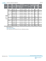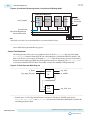
1
SerialLite III Streaming MegaCore
Function User Guide
Last updated for Altera Complete Design Suite: 15.0
UG-01126
Subscribe
2015.05.04
Send Feedback
101 Innovation Drive
San Jose, CA 95134
www.altera.com
TOC-2
Contents
SerialLite III Streaming MegaCore Function Quick Reference......................... 1-1
About the SerialLite III Streaming IP Core........................................................2-1
SerialLite III Streaming Protocol............................................................................................................... 2-1
SerialLite III Streaming Protocol Operating Modes................................................................... 2-2
Performance and Resource Utilization.....................................................................................................2-3
Getting Started ....................................................................................................3-1
Installing and Licensing IP Cores.............................................................................................................. 3-1
OpenCore Plus IP Evaluation.................................................................................................................... 3-1
Specifying IP Core Parameters and Options............................................................................................3-2
SerialLite III Parameter Editor....................................................................................................... 3-2
Arria 10 Designs...............................................................................................................................3-3
SerialLite III Streaming IP Core Parameters............................................................................................3-3
Transceiver Reconfiguration Controller for Stratix V and Arria V GZ Designs................................ 3-5
Files Generated for Altera IP Cores...........................................................................................................3-6
Files Generated for Altera IP Cores (Legacy Parameter Editor)........................................................... 3-8
Simulating..................................................................................................................................................... 3-9
Simulating Altera IP Cores in other EDA Tools..........................................................................3-9
Simulation Parameters.................................................................................................................. 3-10
Arria 10 Simulation Testbench.................................................................................................... 3-12
Simulating and Verifying the Design.......................................................................................... 3-13
SerialLite III Streaming IP Core Functional Description.................................. 4-1
IP Core Architecture....................................................................................................................................4-1
SerialLite III Streaming Source Core.............................................................................................4-3
SerialLite III Streaming Sink Core.................................................................................................4-6
SerialLite III Streaming Duplex Core............................................................................................4-9
Arria 10 versus Stratix V and Arria V GZ Variations.................................................................4-9
Clock Domains...........................................................................................................................................4-10
Core Clocking.................................................................................................................................4-11
Core Latency...................................................................................................................................4-14
Transmission Overheads and Lane Rate Calculations......................................................................... 4-15
Reset.............................................................................................................................................................4-16
Link-Up Sequence......................................................................................................................................4-16
CRC-32 Error Injection ........................................................................................................................... 4-17
FIFO ECC Protection ............................................................................................................................... 4-17
User Data Interface Waveforms.............................................................................................................. 4-17
Signals..........................................................................................................................................................4-19
Altera Corporation
TOC-3
SerialLite III Streaming IP Core Design Guidelines.......................................... 5-1
SerialLite III Streaming IP Core Design Example for Stratix V Devices..............................................5-1
Design Example Components........................................................................................................5-3
Design Setup .................................................................................................................................... 5-4
Design Example Compilation and Download............................................................................. 5-5
Design Example Operation.............................................................................................................5-6
SerialLite III Streaming Link Debugging..................................................................................................5-6
Source Core Link Debugging......................................................................................................... 5-7
Sink Core Link Debugging............................................................................................................. 5-9
Error Handling...........................................................................................................................................5-10
Additional Information...................................................................................... 6-1
Document Revision History ...................................................................................................................... 6-1
How to Contact Altera................................................................................................................................ 6-1
Altera Corporation
1
SerialLite III Streaming MegaCore Function
Quick Reference
2015.05.04
UG-01126
Subscribe
Send Feedback
The Altera® SerialLite III Streaming MegaCore® IP function is a lightweight protocol suitable for high
bandwidth streaming data in chip-to-chip, board-to-board, and backplane applications.
The SerialLite III Streaming IP core is part of the MegaCore IP Library, which is distributed with the
Quartus® II software and is downloadable from the Altera website at www.altera.com.
Note: For system requirements and installation instructions, refer to the Altera Software Installation and
Licensing Manual.
Table 1-1: SerialLite III Streaming MegaCore Function
Item
Release
Information
Description
Version
15.0
Release Date
May 2015
IP Catalog
Name
• Arria 10 SerialLite III Streaming (Arria 10 devices)
• SerialLite III Streaming (Stratix V and Arria V GZ devices)
Ordering
Code
IP-SLITE3/ST
Product ID
010A
Vendor ID
6AF7
© 2015 Altera Corporation. All rights reserved. ALTERA, ARRIA, CYCLONE, ENPIRION, MAX, MEGACORE, NIOS, QUARTUS and STRATIX words and logos are
trademarks of Altera Corporation and registered in the U.S. Patent and Trademark Office and in other countries. All other words and logos identified as
trademarks or service marks are the property of their respective holders as described at www.altera.com/common/legal.html. Altera warrants performance
of its semiconductor products to current specifications in accordance with Altera's standard warranty, but reserves the right to make changes to any
products and services at any time without notice. Altera assumes no responsibility or liability arising out of the application or use of any information,
product, or service described herein except as expressly agreed to in writing by Altera. Altera customers are advised to obtain the latest version of device
specifications before relying on any published information and before placing orders for products or services.
www.altera.com
101 Innovation Drive, San Jose, CA 95134
ISO
9001:2008
Registered
1-2
UG-01126
2015.05.04
SerialLite III Streaming MegaCore Function Quick Reference
Item
Description
Core Features • Up to 17.4 Gbps lane data rates for Arria 10 devices.
• Supports 1–24 serial lanes in configurations that provide nominal
bandwidths from 3.125 gigabits per second (Gbps) to over 300 Gbps.
• Avalon® Streaming (Avalon-ST) user interfaces on the transmit and
receive datapaths.
IP Core
Information
Protocol
Features
•
•
•
•
•
•
•
Simplex and duplex operations
Support for single or multiple lanes
64B/67B physical layer encoding
Payload and idle scrambling
Error detection
Low overhead framing
Low point-to-point transfer latency
Typical
Application
•
•
•
•
High resolution video
Radar processing
Medical imaging
Baseband processing in wireless infrastructure
Device Family Arria 10, Arria V GZ, and Stratix V FPGA devices.
Support
Refer to the What’s New in Altera IP page of the Altera website for
detailed information.
Design Tools
• Parameter editor in the Quartus II software for IP design instantiation
and compilation
• TimeQuest timing analyzer in the Quartus II software for timing
analysis
• ModelSim-Altera software, MATLAB, or third-party tool using
NativeLink for design simulation or synthesis
Related Information
• Altera Software Installation and Licensing
• What's New in Altera IP
Altera Corporation
SerialLite III Streaming MegaCore Function Quick Reference
Send Feedback
2
About the SerialLite III Streaming IP Core
2015.05.04
UG-01126
Subscribe
Send Feedback
The SerialLite III Streaming IP core is a high-speed serial communication protocol for chip-to-chip,
board-to-board, and backplane application data transfers. This protocol offers high bandwidth, low
overhead frames, low I/O count, and supports scalability in both number of lanes and lane speed.
The SerialLite III Streaming IP core incorporates a physical coding sublayer (PCS), a physical media
attachment (PMA), and a media access control (MAC) block. The IP core transmits and receives
streaming data through the Avalon-ST interface on its FPGA fabric interface.
Figure 2-1: Typical System Application
FPGA
Interface Board
ADC
or
System Board
User
Logic
FPGA
Serial Data
(Up to
24 Channels)
SerialLite III
Streaming
MegaCore
Function
Control Board
SerialLite III
Streaming
MegaCore
Function
User
Logic
Data Processing
or
Management Board
Transmission
Media Support:
- PCB (Chip-to-Chip)
- Backplane (Board-to-Board)
SerialLite III Streaming Protocol
The SerialLite III Streaming IP core implements a protocol which supports the transfer of high bandwidth
streaming data over a unidirectional or bidirectional, high-speed serial link.
The SerialLite III Streaming IP core has the following protocol features:
•
•
•
•
•
Simplex and duplex operations
Support for single or multiple lanes
64B/67B physical layer encoding
Payload and idle scrambling
Error detection
© 2015 Altera Corporation. All rights reserved. ALTERA, ARRIA, CYCLONE, ENPIRION, MAX, MEGACORE, NIOS, QUARTUS and STRATIX words and logos are
trademarks of Altera Corporation and registered in the U.S. Patent and Trademark Office and in other countries. All other words and logos identified as
trademarks or service marks are the property of their respective holders as described at www.altera.com/common/legal.html. Altera warrants performance
of its semiconductor products to current specifications in accordance with Altera's standard warranty, but reserves the right to make changes to any
products and services at any time without notice. Altera assumes no responsibility or liability arising out of the application or use of any information,
product, or service described herein except as expressly agreed to in writing by Altera. Altera customers are advised to obtain the latest version of device
specifications before relying on any published information and before placing orders for products or services.
www.altera.com
101 Innovation Drive, San Jose, CA 95134
ISO
9001:2008
Registered
2-2
UG-01126
2015.05.04
SerialLite III Streaming Protocol Operating Modes
• Low protocol overhead
• Low point-to-point transfer latency
• Uses the hardened Native PHY IP core (Arria 10 devices) or Interlaken PHY IP core (Stratix V and
Arria V GZ devices) to reduce soft logic resource utilization
SerialLite III Streaming Protocol Operating Modes
The protocol defines two operating modes for different applications: continuous and burst mode. This
section defines these two operating modes, and describes the targeted application models and their key
characteristics. The following table shows the key differences of the two operating modes.
Table 2-1: Continuous vs. Burst Mode Characteristics
Characteristics
Continuous Mode
Burst Mode
Buffering
Minimal
Burst size
Can connect directly to a data converter (ADC,
DAC)
Yes
No
Asynchronous clock and data recovery support
No
Yes
The IP core that you generate can be in either mode. There is no parameter option to select between
continuous and burst modes. The selection depends on how you provide data at the Avalon-ST TX
interface.
Continuous Mode
A SerialLite III Streaming link operating in continuous mode accepts and transmits user data over the
link, and presents it on the user interface at the receiving link at the same rate and without gaps in the
stream. When operating in this mode, a link implementing the protocol looks like a data pipe that can
transparently forward all data presented on the user interface to the far end of the link.
Continuous mode is appropriate for applications that require a simple interface to transmit a single, high
bandwidth data stream. An example of this application is sensor data links for radar and wireless
infrastructure. With this mode, data converters can connect to either end of the link with minimal
interface logic. This mode requires both ends of the link to operate from a common transceiver reference
clock.
Burst Mode
A SerialLite III Streaming link operating in burst mode accepts bursts of data across the user interface and
transmits each burst across the link as a discrete data burst.
Burst mode is appropriate for applications where the data stream is divided into bursts of data. An
example of this application is uncompressed digital video where the data stream is divided into lines of
display raster. This mode provides more flexibility to the clocking and also supports multiplexing of
multiple data streams across the link.
Note: The minimum required gap between bursts is 2 user clock cycles in standard and advanced
clocking modes on the transmit side. Therefore, the user must provide two extra user clock cycles
between an end of burst and the start of the next burst.
Altera Corporation
About the SerialLite III Streaming IP Core
Send Feedback
UG-01126
2015.05.04
2-3
Performance and Resource Utilization
Related Information
• Standard Clocking Mode on page 4-12
• Advanced Clocking Mode on page 4-13
Performance and Resource Utilization
The following table lists the resources and expected performance for different SerialLite III Streaming IP
core variations. These results are obtained using the Quartus II software targeting the Stratix V GX
(5SGXMA7H2F35C2), the Arria V GZ (5AGZME7K2F40I3L), and the Arria 10 (10AX115S1F45I1SGES)
FPGA device.
Note: The numbers of ALMs and logic registers in the following table are rounded up to the nearest 100.
Table 2-2: SerialLite III Streaming IP Core FPGA Performance and Resource Utilization
Parameters
Device
Direction
Source
Sink
Arria
10
Duplex
Clocking
Mode
Number
of Lanes
Per-Lane
Data Rate
(Mbps)
Standard
24
17400
Disabled
1984
3937
259
48
Standard
24
17400
Enabled
2818
5696
902
72
Advanced 24
17400
Disabled
2378
4009
219
87
Advanced 24
17400
Enabled
4003
8412
910
121
Standard
24
17400
Disabled
2930
7409
373
48
Standard
24
17400
Enabled
3673
9047
1052
72
Advanced 24
17400
Disabled
4060
7363
452
0
Advanced 24
17400
Enabled
3860
9084
1083
72
Standard
24
17400
Disabled
4226
10838
561
96
Standard
24
17400
Enabled
5775
14442
1726
144
Advanced 24
17400
Disabled
6032
10836
623
87
Advanced 24
17400
Enabled
7266
16808
1996
193
About the SerialLite III Streaming IP Core
Send Feedback
Logic Registers
ECC
ALMs
Primary Secondary
M20K
Altera Corporation
2-4
UG-01126
2015.05.04
Performance and Resource Utilization
Parameters
Device
Direction
Source
Stratix Sink
V GX
and
Arria
V GZ
Duplex
Clocking
Mode
Logic Registers
Number
of Lanes
Per-Lane
Data Rate
(Mbps)
ECC
Standard
24
10312.50
Disabled
6257
4511
142
48
Standard
24
10312.50
Enabled
7191
6636
459
72
Advanced 24
10312.50
Disabled
6265
4482
196
87
Advanced 24
10312.50
Enabled
8038
9013
761
121
Standard
24
10312.50
Disabled
5159
7962
267
48
Standard
24
10312.50
Enabled
3779
9761
802
72
Advanced 24
10312.50
Disabled
6058
7995
258
0
Advanced 24
10312.50
Enabled
5891
9789
905
72
Standard
24
10312.50
Disabled
4680
11819
482
96
Standard
24
10312.50
Enabled
6419
15829
1249
144
Advanced 24
10312.50
Disabled
5582
11779
514
87
Advanced 24
10312.50
Enabled
7018
18393
1410
193
ALMs
Primary Secondary
M20K
Related Information
Fitter Resources Reports
More information about Quartus II resource utilization reporting.
Altera Corporation
About the SerialLite III Streaming IP Core
Send Feedback
Getting Started
3
2015.05.04
UG-01126
Subscribe
Send Feedback
Installing and Licensing IP Cores
The Altera IP Library provides many useful IP core functions for your production use without purchasing
an additional license. Some Altera MegaCore® IP functions require that you purchase a separate license
for production use. However, the OpenCore® feature allows evaluation of any Altera® IP core in
simulation and compilation in the Quartus® II software. After you are satisfied with functionality and
perfformance, visit the Self Service Licensing Center to obtain a license number for any Altera product.
Figure 3-1: IP Core Installation Path
acds
quartus - Contains the Quartus II software
ip - Contains the Altera IP Library and third-party IP cores
altera - Contains the Altera IP Library source code
<IP core name> - Contains the IP core source files
Note: The default IP installation directory on Windows is <drive>:\altera\<version number>; on Linux it is
<home directory>/altera/ <version number>.
Related Information
• Altera Licensing Site
• Altera Software Installation and Licensing Manual
OpenCore Plus IP Evaluation
Altera's free OpenCore Plus feature allows you to evaluate licensed MegaCore IP cores in simulation and
hardware before purchase. You need only purchase a license for MegaCore IP cores if you decide to take
your design to production. OpenCore Plus supports the following evaluations:
•
•
•
•
Simulate the behavior of a licensed IP core in your system.
Verify the functionality, size, and speed of the IP core quickly and easily.
Generate time-limited device programming files for designs that include IP cores.
Program a device with your IP core and verify your design in hardware.
© 2015 Altera Corporation. All rights reserved. ALTERA, ARRIA, CYCLONE, ENPIRION, MAX, MEGACORE, NIOS, QUARTUS and STRATIX words and logos are
trademarks of Altera Corporation and registered in the U.S. Patent and Trademark Office and in other countries. All other words and logos identified as
trademarks or service marks are the property of their respective holders as described at www.altera.com/common/legal.html. Altera warrants performance
of its semiconductor products to current specifications in accordance with Altera's standard warranty, but reserves the right to make changes to any
products and services at any time without notice. Altera assumes no responsibility or liability arising out of the application or use of any information,
product, or service described herein except as expressly agreed to in writing by Altera. Altera customers are advised to obtain the latest version of device
specifications before relying on any published information and before placing orders for products or services.
www.altera.com
101 Innovation Drive, San Jose, CA 95134
ISO
9001:2008
Registered
3-2
Specifying IP Core Parameters and Options
UG-01126
2015.05.04
OpenCore Plus evaluation supports the following two operation modes:
• Untethered—run the design containing the licensed IP for a limited time.
• Tethered—run the design containing the licensed IP for a longer time or indefinitely. This requires a
connection between your board and the host computer.
Note: All IP cores that use OpenCore Plus time out simultaneously when any IP core in the design times
out.
Specifying IP Core Parameters and Options
Follow these steps to specify IP core parameters and options.
1. In the Qsys IP Catalog (Tools > IP Catalog), locate and double-click the name of the IP core to
customize. The parameter editor appears.
2. Specify a top-level name for your custom IP variation. This name identifies the IP core variation files
in your project. If prompted, also specify the target Altera device family and output file HDL
preference. Click OK.
3. Specify parameters and options for your IP variation:
• Optionally select preset parameter values. Presets specify all initial parameter values for specific
applications (where provided).
• Specify parameters defining the IP core functionality, port configurations, and device-specific
features.
• Specify options for generation of a timing netlist, simulation model, testbench, or example design
(where applicable).
• Specify options for processing the IP core files in other EDA tools.
4. Click Finish to generate synthesis and other optional files matching your IP variation specifications.
The parameter editor generates the top-level .qsys IP variation file and HDL files for synthesis and
simulation. Some IP cores also simultaneously generate a testbench or example design for hardware
testing.
The top-level IP variation is added to the current Quartus II project. Click Project > Add/Remove Files
in Project to manually add a .qsys file to a project. Make appropriate pin assignments to connect ports.
SerialLite III Parameter Editor
Based on the values you set, the SerialLite III streaming parameter editor automatically calculates the rest
of the parameters, and provides you with the following values or information:
•
•
•
•
Input data rate per lane
Transceiver data rate per lane
A list of feasible transceiver reference clock frequencies, one of which you select to provide to the core
Information related to the core overheads
Important: If your design targets Stratix V or Arria V GZ devices, you cannot migrate your design to
Arria 10 devices automatically. For Arria 10 devices, the transceiver reconfiguration
functionality is embedded inside the transceivers. Therefore, you must re-instantiate the IP
core to target Arria 10 devices.
Related Information
SerialLite III Streaming IP Core Parameters on page 3-3
Altera Corporation
Getting Started
Send Feedback
UG-01126
2015.05.04
Arria 10 Designs
3-3
Arria 10 Designs
If your design targets Arria 10 devices:
• The parameter editor displays a message about the required output clock frequency of the external TX
PLL IP clock. For source or duplex modes, connect the Transceiver PHY Reset Controller to the TX
PLL to ensure the appropriate HSSI power-up sequence.
• For source only Arria 10 implementations, the parameter editor does not provide the transceiver
reference clock frequency because the user is expected to provide the transmit serial clock. If you use
an on-chip PLL to generate the transmit serial clock, you can use the same PLL reference clock
frequency that you provide to the core in the sink direction, operating at the same user clock frequency
(or equivalent transceiver lane data rate).
• The SerialLite IP core expects the user to provide the transmitter's serial clock. If you compile the IP
without the proper serial clock, the Quartus II Compiler issues a compilation error. Refer to Arria 10
Simulation Testbench for an example design.
• When generating the example testbench, the SerialLite IP core instantiates an external transceiver ATX
PLL for the transmit serial clock based on the required user clock only when configured in sink or
duplex mode. The Arria 10 simulation testbench uses the external transceiver ATX PLL. The
transceiver ATX PLL core is configured with the transceiver reference clock specified in the parameter
editor and transmit serial clock.
• To generate the SerialLite III Arria 10 example testbench using the parameter editor, select Generate >
Example Designs > seriallite_iii_a10_0 - example (alternatively, turn on the Example Design option
in the parameter editor). Altera recommends that you generate the Arria 10 simulation testbench for
the sink or duplex direction.
Related Information
• SerialLite III Streaming IP Core Parameters on page 3-3
• Arria 10 Simulation Testbench on page 3-12
• Arria 10 versus Stratix V and Arria V GZ Variations on page 4-9
SerialLite III Streaming IP Core Parameters
Table 3-1: SerialLite III Streaming IP Core Parameters
Parameter
Value
Default
Description
General Design Options
Direction
Source, Sink,
Duplex
Duplex
Indicates the direction of the core's variant.
Lanes
1–24
4
Specifies the number of lanes (equal to physical
transceiver links) that are used to transfer the
streaming data.
Device speed
grade
1–4
2
Specifies the device speed grade (Stratix V and
Arria V GZ devices only).
PLL type
ATX, CMU
CMU
Selects the transceiver PLL type. (Stratix V and
Arria V GZ devices only)
Getting Started
Send Feedback
Altera Corporation
3-4
UG-01126
2015.05.04
SerialLite III Streaming IP Core Parameters
Parameter
Value
Default
Description
Meta frame
length
200–8191
8191
Specifies the metaframe length in 8-byte words.
ECC
Protection
Yes/No
No
Select to use error correcting code (ECC)
protection to strengthen the FIFO buffers from
single-event upset (SEU) changes.
No
Select to use the advanced clocking mode for your
design. The default setting is standard clocking
mode.
Clocking and Data Rates
Advanced
Yes/No
clocking mode
Required user Minimum: 50 MHz 146.484375
clock
MHz
Maximum: Limited
frequency
by the supported
transceiver data
rates
Specifies the clock generator’s fractional PLL
(fPLL) output frequency used to drive the user_
clock signal. This range is device-specific and is
tied with the lane data rate and fPLL minimal
clocking constraints.
Generated
user clock
frequency(1)
Minimum: 50 MHz 146.484375
MHz
Maximum: Limited
by the supported
transceiver data
rates
Specifies the actual user clock frequency as
produced by the fPLL and is ideally the same as
the required clock frequency. In certain very high
precision situations where the desired user clock is
provided up to higher decimal places, this value
can vary slightly due to the fPLL constraints.
Change the required clock frequency to correct the
issue if the minute variation is intolerable.
Interface
clock
frequency(1)
Lane rate/64
Specifies the clock frequency of the source, sink, or
duplex user interface in advanced clocking mode.
Lane rate/40
205.078125
MHz
In advanced clocking mode, this signal specifies
the frequency required for the user_clock input.
Arria 10 15.625 Gbps ≤ lane rate ≤ 17.4 Gbps:
Lane rate/64
See description
Arria 10 < 15.625 Gbps, and all Stratix V and Arria
V GZ: Lane rate/40
Core clock
frequency(1)
(Lane rate/64) to
(Lane rate/67)
(Lane rate/40)–to
(Lane rate/67)
See description
205.078125
MHz
The core clock is used internally between the user
domain and the Native PHY IP core (Arria 10
devices) or Interlaken PHY IP core (Stratix V and
Arria V GZ devices).
Arria 10 15.625 Gbps ≤ lane rate ≤ 17.4 Gbps:
(Lane rate/64) to (Lane rate/67)
Arria 10 < 15.625 Gbps, and all Stratix V and Arria
V GZ: (Lane rate/40) to (Lane rate/67) (2)
(1)
The parameter editor automatically calculates this parameter value based on the general design options.
Altera Corporation
Getting Started
Send Feedback
UG-01126
2015.05.04
Transceiver Reconfiguration Controller for Stratix V and Arria V GZ...
Parameter
fPLL
reference
clock
frequency (1)
Value
Default
Lane rate/64
257.812500
MHz
Lane rate/40
3-5
Description
Specifies the fPLL reference clock frequency in
standard clocking mode.
Arria 10 15.625 Gbps ≤ lane rate ≤ 17.4 Gbps: lane
rate/64
See description
Arria 10 < 15.625 Gbps, and all Stratix V and Arria
V GZ: Lane rate/40 (2)
Transceiver
reference
clock
frequency
Range supported
644.53125
by the transceiver
MHz
PLLs (Lane rate/N)
Specifies the transceiver reference clock frequency.
The default value for the Input clock frequency is
lane rate/16. Sample values of N include 80, 64, 50,
40, 32, 25, 20, 16, 12.5, 10, and 8.
Altera recommends that you select the highest
frequency among the available options in the
drop-down list.
For Arria 10 source designs, set this parameter to
none.
Input data
64 × (User clock
rate per lane(1) frequency)
9.375 Gbps
Input data rate that the core can support.
Transceiver
data rate per
lane(1)
10.3125 Gbps
The effective data rate at the output of the
transceivers, incorporating transmission and other
overheads.
Input data rate ×
Overheads
The parameter editor automatically calculates this
value by adding the input data rate with transmis‐
sion overheads to provide you with a selection of
user clock frequency.(2)
Aggregate
input data
rate(1)
Lanes × Input data
rate
36.6210938
Gbps
Aggregate input data rate that the core can
support.
Related Information
SerialLite III Parameter Editor on page 3-2
Transceiver Reconfiguration Controller for Stratix V and Arria V GZ
Designs
If your design targets Stratix V or Arria V GZ devices, the transceiver reconfiguration controller is not
included in the generated IP core. To create a complete system, refer to the design example block diagram
on how to connect the transceiver reconfiguration controller.
(2)
The clock frequency value is useful if you want to simulate designs at different data rates. You should
apply the displayed value in your testbench parameters.
Getting Started
Send Feedback
Altera Corporation
3-6
UG-01126
2015.05.04
Files Generated for Altera IP Cores
Note: If your design targets Arria 10 devices, the transceiver reconfiguration functionality is embedded
inside the transceivers. The phy_mgmt bus interface connects directly to the Avalon-MM dynamic
reconfiguration interface of the embedded Arria 10 Native PHY IP core. This interface is provided
at the top level.
Files Generated for Altera IP Cores
The Quartus II software generates the following IP core output file structure:
Figure 3-2: IP Core Generated Files
<project directory>
<your_ip>.qsys - System or IP integration file
<your_ip>.sopcinfo - Software tool-chain integration file
<your_ip>
<your_ip> n
<testbench>_tb
IP variation files
IP variation files
testbench system
<your_ip>_tb.qsys
Testbench system file
<your_ip>.cmp - VHDL component declaration file
<your_ip>_bb.v - Verilog HDL black box EDA synthesis file
<your_ip>_inst.v or .vhd - Sample instantiation template
<your_ip>.ppf - XML I/O pin information file
<testbench>_tb
testbench files
<your_ip>.qip - Lists IP synthesis files
<your_testbench>_tb.csv
<your_ip>.sip - Contains assingments for IP simulation files
<your_testbench>_tb.spd
<your_ip>_generation.rpt - IP generation report
<your_ip>.debuginfo - Contains post-generation information
<your_ip>.html - Connection and memory map data
sim
simulation files
<your_ip>.bsf - Block symbol schematic
<your_ip>.spd - Combines simulation scripts for multiple cores
<EDA tool setup
scripts>
sim
synth
Simulation files
IP synthesis files
<your_ip>.v or .vhd
Top-level simulation file
<EDA tool name>
Simulator scripts
<simulator_setup_scripts>
<ip subcores> n
Subcore libraries
<your_ip>.v or .vhd
Top-level IP synthesis file
synth
Subcore
synthesis files
sim
Subcore
Simulation files
<HDL files>
<HDL files>
Table 3-2: IP Core Generated Files
File Name
<my_ip>.qsys
Altera Corporation
Description
The Qsys system or top-level IP variation file. <my_ip> is the name
that you give your IP variation.
Getting Started
Send Feedback
UG-01126
2015.05.04
Files Generated for Altera IP Cores
File Name
<system>.sopcinfo
3-7
Description
Describes the connections and IP component parameterizations in
your Qsys system. You can parse its contents to get requirements
when you develop software drivers for IP components.
Downstream tools such as the Nios II tool chain use this file.
The .sopcinfo file and the system.h file generated for the Nios II tool
chain include address map information for each slave relative to each
master that accesses the slave. Different masters may have a different
address map to access a particular slave component.
<my_ip>.cmp
The VHDL Component Declaration (.cmp) file is a text file that
contains local generic and port definitions that you can use in VHDL
design files.
<my_ip>.html
A report that contains connection information, a memory map
showing the address of each slave with respect to each master to
which it is connected, and parameter assignments.
<my_ip>_generation.rpt
IP or Qsys generation log file. A summary of the messages during IP
generation.
<my_ip>.debuginfo
Contains post-generation information. Used to pass System Console
and Bus Analyzer Toolkit information about the Qsys interconnect.
The Bus Analysis Toolkit uses this file to identify debug components
in the Qsys interconnect.
<my_ip>.qip
Contains all the required information about the IP component to
integrate and compile the IP component in the Quartus II software.
<my_ip>.csv
Contains information about the upgrade status of the IP component.
<my_ip>.bsf
A Block Symbol File (.bsf) representation of the IP variation for use
in Quartus II Block Diagram Files (.bdf).
<my_ip>.spd
Required input file for ip-make-simscript to generate simulation
scripts for supported simulators. The .spd file contains a list of files
generated for simulation, along with information about memories
that you can initialize.
<my_ip>.ppf
The Pin Planner File (.ppf) stores the port and node assignments for
IP components created for use with the Pin Planner.
<my_ip>_bb.v
You can use the Verilog black-box (_bb.v) file as an empty module
declaration for use as a black box.
<my_ip>.sip
Contains information required for NativeLink simulation of IP
components. You must add the .sip file to your Quartus project.
<my_ip>_inst.v or _inst.vhd
HDL example instantiation template. You can copy and paste the
contents of this file into your HDL file to instantiate the IP variation.
Getting Started
Send Feedback
Altera Corporation
3-8
UG-01126
2015.05.04
Files Generated for Altera IP Cores (Legacy Parameter Editor)
File Name
Description
<my_ip>.regmap
If the IP contains register information, the .regmap file generates.
The .regmap file describes the register map information of master
and slave interfaces. This file complements the .sopcinfo file by
providing more detailed register information about the system. This
enables register display views and user customizable statistics in
System Console.
<my_ip>.svd
Allows HPS System Debug tools to view the register maps of
peripherals connected to HPS within a Qsys system.
During synthesis, the .svd files for slave interfaces visible to System
Console masters are stored in the .sof file in the debug section.
System Console reads this section, which Qsys can query for register
map information. For system slaves, Qsys can access the registers by
name.
<my_ip>.v
or
HDL files that instantiate each submodule or child IP core for
synthesis or simulation.
<my_ip>.vhd
mentor/
Contains a ModelSim® script msim_setup.tcl to set up and run a
simulation.
aldec/
Contains a Riviera-PRO script rivierapro_setup.tcl to setup and run a
simulation.
/synopsys/vcs
Contains a shell script vcs_setup.sh to set up and run a VCS®
simulation.
/synopsys/vcsmx
Contains a shell script vcsmx_setup.sh and synopsys_ sim.setup file to
set up and run a VCS MX® simulation.
/cadence
Contains a shell script ncsim_setup.sh and other setup files to set up
and run an NCSIM simulation.
/submodules
Contains HDL files for the IP core submodule.
<child IP cores>/
For each generated child IP core directory, Qsys generates /synth and /
sim sub-directories.
Files Generated for Altera IP Cores (Legacy Parameter Editor)
The Quartus II generates the following output for IP cores that use the legacy MegaWizard parameter
editor.
Altera Corporation
Getting Started
Send Feedback
UG-01126
2015.05.04
Simulating
3-9
Figure 3-3: IP Core Generated Files
<Project Directory>
<your_ip>.qip - Quartus II IP integration file
<your_ip>.v or .vhd - Top-level IP synthesis file
<your_ip>_bb.v - Verilog HDL black box EDA synthesis file
<your_ip>.bsf - Block symbol schematic file
<your_ip>_syn.v or .vhd - Timing & resource estimation netlist 1
<your_ip>.vo or .vho - IP functional simulation model 2
<your_ip>_inst.v or .vhd - Sample instantiation template
<your_ip>.cmp - VHDL component declaration file
greybox_tmp 3
Notes:
1. If supported and enabled for your IP variation
2. If functional simulation models are generated
3. Ignore this directory
Simulating
Simulating Altera IP Cores in other EDA Tools
The Quartus II software supports RTL and gate-level design simulation of Altera IP cores in supported
EDA simulators. Simulation involves setting up your simulator working environment, compiling
simulation model libraries, and running your simulation.
You can use the functional simulation model and the testbench or example design generated with your IP
core for simulation. The functional simulation model and testbench files are generated in a project
subdirectory. This directory may also include scripts to compile and run the testbench. For a complete list
of models or libraries required to simulate your IP core, refer to the scripts generated with the testbench.
You can use the Quartus II NativeLink feature to automatically generate simulation files and scripts.
NativeLink launches your preferred simulator from within the Quartus II software.
Getting Started
Send Feedback
Altera Corporation
3-10
UG-01126
2015.05.04
Simulation Parameters
Figure 3-4: Simulation in Quartus II Design Flow
Design Entry
(HDL, Qsys, DSP Builder)
Altera Simulation
Models
Quartus II
Design Flow
Gate-Level Simulation
Analysis & Synthesis
Fitter
(place-and-route)
TimeQuest Timing Analyzer
RTL Simulation
EDA
Netlist
Writer
Post-synthesis functional
simulation netlist
Post-synthesis
functional
simulation
Post-fit functional
simulation netlist
Post-fit functional
simulation
Post-fit timing
simulation netlist
(Optional)
Post-fit
Post-fit timing
timing
simulation
simulation
(3)
Device Programmer
Note: Post-fit timing simulation is supported only for Stratix IV and Cyclone IV devices in the current
version of the Quartus II software. Altera IP supports a variety of simulation models, including
simulation-specific IP functional simulation models and encrypted RTL models, and plain text
RTL models. These are all cycle-accurate models. The models support fast functional simulation of
your IP core instance using industry-standard VHDL or Verilog HDL simulators. For some cores,
only the plain text RTL model is generated, and you can simulate that model. Use the simulation
models only for simulation and not for synthesis or any other purposes. Using these models for
synthesis creates a nonfunctional design.
Related Information
Simulating Altera Designs
Simulation Parameters
After design generation, simulation files are available for you to simulate your design. To simulate your
design, ensure that the SerialLite III Streaming IP core source and sink cores are both generated with the
same parameters or are duplex cores.
• Stratix V and Arria V GZ files are located in the <variation name>_sim directory
• Arria 10 files are located in the <variation name> directory
The example testbench simulates the core using the user-specified configuration
Altera Corporation
Getting Started
Send Feedback
UG-01126
2015.05.04
Simulation Parameters
3-11
Table 3-3: Stratix V and Arria V GZ Testbench Default Simulation Parameters
Parameter
Default Value
Generated user clock
frequency (user_clock_
frequency)
Standard clocking: 145.98375
MHz
Lanes (lanes)
2
Comments
—
Advanced clocking:
146.484375
—
Transceiver reference clock 644.53125 MHz
frequency (pll_ref_freq)
—
Transceiver data rate per
lane (data_rate)
10312.5 Mbps
—
Meta frame length (meta_
200
—
fPLL reference clock
frequency (reference_
clock_frequency)
257.8125 MHz
Not used in advanced clocking mode.
Core clock frequency
(coreclkin_frequency)
205.078125 MHz
Not used in advanced clocking mode.
frame_length)
Simulation-specific parameters
Total samples to transfer
(total_samples_to_
transfer)
2000
Total samples to transfer during simulation.
Mode (mode)
Continuous/burst
The testbench environment may automati‐
cally choose one of the modes depending on
the random seed with which it is provided.
Refer to the simulation scripts listed in
Table 3-4 for details.
Skew insertion enable
Yes
(skew_insertion_enable)
Skew testing is enabled. The testbench
environment randomly inserts skew in the
lanes within the range 0 - 107 UI.
ECC protection enabled
(ecc_enable)
When set, the core is simulated with the
ECC-enabled variant. Use the ECC-enabled
variant in the test environment.
0
When ECC mode is disabled, the two most
significant bits of the error buses in the
source or sink direction are don't care.
For more information about Altera simulation models, refer to the Simulating Altera Designs chapter in
volume 3 of the Quartus II Handbook.
Related Information
Simulating Altera Designs
Getting Started
Send Feedback
Altera Corporation
3-12
UG-01126
2015.05.04
Arria 10 Simulation Testbench
Arria 10 Simulation Testbench
If your design targets Arria 10 devices, the generated example testbench is dynamic and has the same
configuration as the IP (except for the metaframe length). When you choose the sink or duplex direction,
the parameter editor generates an external transceiver ATX PLL for use in the Arria 10 testbench.
Therefore, Altera recommends that you generate the Arria 10 simulation testbench for designs using the
sink or duplex direction.
Note: The Arria 10 example testbench includes the external transceiver PLL; the IP core does not include
the transceiver PLL for these devices.
Figure 3-5: SerialLite III Streaming Example Testbench (Duplex) for Arria 10 Devices
Test Environment
Device Under Test (Duplex Mode)
Traffic
Generator
Source
Absorber
Source
Application
Loopback
Source
Clock
Generator
Testbench
Traffic
Checker
Sink
Application
Transceiver
TX PLL
Source
Adaptation
Sink
Adaptation
Sink
Alignment
Native
PHY IP
Duplex Interlaken
Mode
Skew
Insertion
Sink
Clock
Generator
Altera Corporation
Getting Started
Send Feedback
UG-01126
2015.05.04
Simulating and Verifying the Design
3-13
Figure 3-6: SerialLite III Streaming Example Testbench (Simplex) for Arria 10 Devices
Test Environment
Device Under Test (Source)
Traffic
Generator
Source
Absorber
Source
Application
Source
Adaptation
Loopback
Source
Clock
Generator
Native
PHY IP
TX Interlaken
Mode
Transceiver
TX PLL
Testbench
Device Under Test (Sink)
Traffic
Checker
Sink
Application
Sink
Clock
Generator
Sink
Adaptation
Sink
Alignment
Native
PHY IP
RX Interlaken
Mode
Skew
Insertion
Simulating and Verifying the Design
1. Set the environment variables:
• QUARTUS_ROOTDIR to the location of the Quartus II software directory.
• For ModelSim-Altera only: MODELSIM_ALTERA_LIBS to the location of the precompiled
simulation libraries.
2. For simplex mode, set the following environment variables:
• SRC_SIM_LOCATION to the location where the simulation files for the source core are generated.
For instance, if the name of the source core is 'src', then the directory name is /src_sim for Stratix V
and Arria V GZ devices and /src for Arria 10 devices.
• SNK_SIM_LOCATION to the location where the simulation files for sink core are generated. For
instance, if the name of the sink core is 'snk', then the directory name is /snk_sim for Stratix V and
Arria V GZ devices and /snk for Arria 10 devices.
3. For duplex mode, set the following environment variable:
• SIM_LOCATION to the location where the simulation files for the duplex core are generated. For
instance, if the name of the duplex core is 'duplex', then the directory name is /duplex_sim for
Stratix V and Arria V GZ devices and /duplex for Arria 10 devices.
4. Set the parameters in the test_env.v file to override the testbench default value (optional).
5. Run the provided scripts to simulate the testbench in the ModelSim-Altera SE/AE, VCS, VCS MX,
NCSim, or Aldec Riviera simulators. The following table lists the provided scripts.
Getting Started
Send Feedback
Altera Corporation
3-14
UG-01126
2015.05.04
Simulating and Verifying the Design
Table 3-4: Testbench Simulation Scripts
Simulator
ModelSimAltera SE/
AE
VCS/VCS
MX
NCSim
Aldec
Riviera
Device Family
File Directory
<example design name>/example_testbench/vsim/ Arria 10
<variation name>_example/seriallite_iii_sv/
example_testbench/vsim/
Stratix V
<example design name>/example_testbench/vcs/
Arria 10
<variation name>_example/seriallite_iii_sv/
example_testbench/vcs/
Stratix V
<example design name>/example_testbench/
ncsim/
Arria 10
<variation name>_example/seriallite_iii_sv/
example_testbench/ncsim/
Stratix V
Arria V GZ
Script
vsim -c -do
run_vsim.do
run_vcs.sh
Arria V GZ
run_ncsim.sh
Arria V GZ
<example design name>/example_testbench/aldec/ Arria 10
<variation name>_example/seriallite_iii_sv/
example_testbench/aldec/
Stratix V
run_aldec.sh
Arria V GZ
By default, the parameter editor generates simulator-specific scripts containing commands to compile,
elaborate, and simulate Altera IP models and simulation model library files. You can copy the commands
into your simulation testbench script, or edit these files to add commands for compiling, elaborating, and
simulating your design and testbench.
Table 3-5: Altera IP Core Simulation Scripts
Simulator
ModelSimAltera SE/
AE
File Directory
<variation name>_sim/mentor
<variation name>/sim/mentor
Arria 10
<variation name>_sim/synopsys/vcs
Stratix V
Arria V GZ
<variation name>/sim/synopsys/vcs
Arria 10
<variation name>_sim/synopsys/vcsmx
Stratix V
Arria V GZ
VCS MX
<variation name>/sim/synopsys/vcsmx
Script
Stratix V
Arria V GZ
VCS
Altera Corporation
Device Family
Arria 10
msim_setup.tcl
vcs_setup.sh
vcsmx_setup.sh
synopsys_sim.setup
Getting Started
Send Feedback
UG-01126
2015.05.04
Simulating and Verifying the Design
Simulator
File Directory
<variation name>_sim/cadence
<variation name>/sim/cadence
Arria 10
<variation name>_sim/aldec
Stratix V
Arria V GZ
<variation name>/sim/aldec
Script
Stratix V
Arria V GZ
NCSim
Aldec
Riviera
Device Family
3-15
ncsim_setup.sh
rivierapro_set.tcl
Arria 10
For more information about Altera simulation models, refer to the Simulating Altera Designs chapter in
volume 3 of the Quartus II Handbook.
Related Information
Simulating Altera Designs
Getting Started
Send Feedback
Altera Corporation
4
SerialLite III Streaming IP Core Functional
Description
2015.05.04
UG-01126
Send Feedback
Subscribe
The SerialLite III Streaming IP core implements a protocol that defines streaming data encapsulation at
the link layer and data encoding at the physical layer. This protocol integrates transparently with existing
hardware and provides a reliable data transfer mechanism in applications that do not need additional
layers between the data link and application.
IP Core Architecture
The SerialLite III Streaming IP core has three variations:
• Source—Formats streaming data from the user application and transmits the data over serial links.
• Sink—Receives the serial stream data from serial links, removes any formatting information, and
delivers the data to the user application.
• Duplex—Composed of both the source and sink cores. The streaming data can be transmitted and
received in both directions.
All three variations include the Altera Transceiver Native PHY IP core (Arria 10 devices) or Interlaken
PHY IP core (Stratix V and Arria V GZ devices) that utilizes hardened PCS and PMA modules. The
source and sink cores use the Native PHY or Interlaken PHY IP core in simplex mode, and the duplex
core uses the Native PHY or Interlaken PHY IP core in duplex mode.
Table 4-1: IP Core Variant and Function
Core
Function
Source
•
•
•
•
Data encapsulation
Generation and insertion of Idle Control Words
Lane striping for multi-lane link
User synchronization and burst marker insertion
Sink
•
•
•
•
•
Multi-lane alignment
Data encapsulation removal
Idle Control Words removal
Lane de-striping
User synchronization and burst marker demultiplexing
© 2015 Altera Corporation. All rights reserved. ALTERA, ARRIA, CYCLONE, ENPIRION, MAX, MEGACORE, NIOS, QUARTUS and STRATIX words and logos are
trademarks of Altera Corporation and registered in the U.S. Patent and Trademark Office and in other countries. All other words and logos identified as
trademarks or service marks are the property of their respective holders as described at www.altera.com/common/legal.html. Altera warrants performance
of its semiconductor products to current specifications in accordance with Altera's standard warranty, but reserves the right to make changes to any
products and services at any time without notice. Altera assumes no responsibility or liability arising out of the application or use of any information,
product, or service described herein except as expressly agreed to in writing by Altera. Altera customers are advised to obtain the latest version of device
specifications before relying on any published information and before placing orders for products or services.
www.altera.com
101 Innovation Drive, San Jose, CA 95134
ISO
9001:2008
Registered
4-2
UG-01126
2015.05.04
IP Core Architecture
Core
Function
Duplex
• Data encapsulation and decapsulation
• Generation and removal of Idle Control Words
• User synchronization and burst marker insertion and deletion
The simplex and duplex cores support the following clocking schemes:
• Standard clocking—This mode is for pure streaming designs in which the core provides input/output
clocks to drive the user logic. Pure streaming operation ensures an exact replica of the output data as it
was presented at the input without any idle cycles at the output (continuous data valid).
• Advanced clocking—This mode allows the core's input interface to be clocked with the user-preferred
clock by trading-off pure streaming operation.
Figure 4-1: SerialLite III Streaming Simplex Core (Standard Clocking)
SerialLite III Streaming Source
Source User
Interface
Application
Module
Source
Reconfiguration
Controller
Interface
Adaptation
Module
SerialLite III Streaming Sink
PHY IP
Transmit
Core (1)
N
Lanes
PHY IP
Receive
Core (1)
Alignment
Module
Adaptation
Module
Application
Module
Sink User
Interface
Sink
Reconfiguration
Controller
Interface
Note:
1. Native PHY IP core for Arria 10 devices and Interlaken PHY IP core for Stratix V and Arria V GZ devices.
Figure 4-2: SerialLite III Streaming Duplex Core (Standard Clocking)
SerialLite III Streaming Source
Application
Module
Source User
Interface
SerialLite III Streaming Sink
N
Lanes
Adaptation
Module
PHY IP
Duplex
Core (1)
Sink User
Interface
Application
Module
Source
Reconfiguration
Controller
Interface
Adaptation
Module
Alignment
Module
N
Lanes
PHY IP
Duplex
Core (1)
Alignment
Module
Adaptation
Module
Note:
1. Native PHY IP core for Arria 10 devices and Interlaken PHY IP core for Stratix V and Arria V GZ devices.
Adaptation
Module
Application
Module
Application
Module
Sink User
Interface
Source User
Interface
Sink
Reconfiguration
Controller
Interface
The block diagram for advanced clocking is similar to standard clocking, however, it also includes a PPM
absorption FIFO at the source user interface.
Related Information
Altera Transceiver PHY IP Core User Guide
Altera Corporation
SerialLite III Streaming IP Core Functional Description
Send Feedback
UG-01126
2015.05.04
SerialLite III Streaming Source Core
4-3
SerialLite III Streaming Source Core
The source core consists of five major functional blocks (the implementation varies depending on the
clocking mode):
•
•
•
•
•
•
Clock generator (in the standard clocking mode)
Source application module
Source adaptation module
Native PHY IP TX core - Interlaken mode (Arria 10 devices)
Interlaken PHY IP TX core (Stratix V and Arria V GZ devices)
PPM-Absorption module (in the advanced clocking mode only)
Figure 4-3: SerialLite III Streaming Source Core (Standard Clocking Mode)
SerialLite III Streaming Source
Source User Interface
Application
Module
Adaptation
Module
PHY IP
Core (2)
SerialLite III
Streaming Link
Core Clock
Source User Clock
Clock
Generator
Transceiver Reconfiguration Clock
Transceiver Reference Clock
or Transmit Serial Clock (1)
Notes:
1. Transceiver reference clock for Stratix V and Arria V GZ devices; transmit serial clock for Arria 10 devices.
2. Native PHY IP core for Arria 10 devices and Interlaken PHY IP core for Stratix V and Arria V GZ devices.
SerialLite III Streaming IP Core Functional Description
Send Feedback
Clock Domains
Altera Corporation
4-4
UG-01126
2015.05.04
Source Clock Generator
Figure 4-4: SerialLite III Streaming Source Core (Advanced Clocking Mode)
SerialLite III Streaming Source
Source User Interface
PPM
Absorber
Module
Application
Module
Adaptation
Module
PHY IP
Core (1)
SerialLite III
Streaming Link
Core Clock
User Interface Clock
Transceiver Reconfiguration Clock
Transceiver Reference Clock
Clock Domains
Note:
1. Native PHY IP core for Arria 10 devices and Interlaken PHY IP core for Stratix V and Arria V GZ devices.
Source PPM-Absorption Module on page 4-6
Source Clock Generator
The clock generator in the source core synthesizes the user clock (user_clock) and core clock signals
(tx_coreclockin) from the Native PHY IP core (Arria 10 devices) or Interlaken PHY IP (Stratix V and
Arria V GZ devices) core's output clock signal (tx_clkout). This clock generator consists of a fractional
PLL and a state machine responsible for clocks generation and reset sequencing. The user_clock_reset
is not released until the fPLL is locked. The module is used in the standard clocking mode only.
Figure 4-5: Clock Generator Block Diagram
tx_clkout
phy_mgmt_clk_reset
Fractional
PLL
user_clock
tx_coreclkin
lock
Reset
State
Machine
user_clock_reset
• For lane rates < 15.625 Gbps and all Stratix V and Arria V GZ devices, the fPLL generates the
user_clock/user_clock_tx and tx_coreclkin based on fixed ratios determined by the SerialLite III
Streaming parameter editor.
Altera Corporation
SerialLite III Streaming IP Core Functional Description
Send Feedback
UG-01126
2015.05.04
Source Application Module
4-5
• For 15.625 Gbps < lane rates < 17.4 Gpbs, the fPLL outputs the user_clock/user_clock_tx based on
a fixed ratio, however, the tx_coreclkin operates at the same frequency as tx_clkout.
Related Information
Sink Clock Generator on page 4-7
Source Application Module
The application module performs the following functions:
• Burst encapsulation—Inserts burst control words into the data stream to define the beginning and the
end of streaming data bursts.
• Idle insertion—Inserts idle control words (in the standard clocking mode) into all lanes of the data
stream interface.
Source Adaptation Module
This module provides adaptation logic between the application module and the Native PHY IP core
(Arria 10 devices) or Interlaken PHY IP (Stratix V and Arria V GZ devices) core. The adaptation module
performs the following functions:
• Rate adaptation—Includes a dual-clock FIFO buffer to cushion the Interlaken PHY IP core's bursty
read requests and to provide a streaming user write interface. The FIFO also transfers streaming data
between the user_clock and tx_coreclkin clock domains (in standard clocking mode).
• Control signal translation—The state machines maps the control signal semantics on the framing
interface (3) to the semantics of the Native PHY or Interlaken PHY IP core TX interface.
• Non-user idle insertion—Inserts non-user idle control words in the absence of user data to manage the
minimum data rate requirements of the Interlaken protocol. The control words are removed by the
sink adaptation module in the SerialLite III link partner.
Interlaken PHY IP TX Core or Native PHY IP TX Core - Interlaken Mode
For Arria 10 devices, this block is an instance of the Native PHY IP core configured for Interlaken - TX
only operation. For lane rates from 15.625 to 17.4 Gbps, inclusive, the PMA width for Interlaken mode is
64 bits. For lane rates less than 15.625 Gbps, the PMA width is 40 bits.
For Stratix V and Arria V devices, the Interlaken PHY IP TX core is an instance of the Interlaken PHY IP
core configured for TX only operation.The core requires a Transceiver Reconfiguration Controller for
transceiver calibration. The number of channels programmed for configuration in the Transceiver
Reconfiguration Controller depends on the IP core's operation mode. For example,
• if the design is a simplex RX only design, the reconfiguration interfaces is equal to the number of lanes.
• if the design is a simplex TX only design or a duplex design, the reconfiguration interfaces is equal to
the number of lanes x 2.
Related Information
• Arria 10 Transceiver PHY User Guide
For more information about the Arria 10 Native PHY IP core.
(3)
The framing interface is to frame every data burst with the Start of Burst, Sync, and End of Burst, and
sequence them to the PHY interface.
SerialLite III Streaming IP Core Functional Description
Send Feedback
Altera Corporation
4-6
UG-01126
2015.05.04
Source PPM-Absorption Module
• Altera Transceiver PHY IP Core User Guide
For more information about the Interlaken PHY IP core and how to dynamically reconfigure the PHY.
Source PPM-Absorption Module
This module is implemented when the SerialLite III Streaming IP core is instantiated with advanced
clocking mode. This module allows you to use your own clock to interface data or to compensate the
clock difference between the user clock and source interface clock (interface_clock).
Related Information
Advanced Clocking Mode on page 4-13
SerialLite III Streaming Sink Core
The sink core consists of five major functional blocks:
•
•
•
•
•
•
Native PHY IP RX core - Interlaken mode (Arria 10 devices)
Interlaken PHY IP RX core (Stratix V or Arria V GZ devices)
Lane alignment module
Clock generator (standard clocking mode only)
Sink adaptation module
Sink application module
Figure 4-6: SerialLite III Streaming Sink Core (Standard Clocking Mode)
SerialLite III Streaming Sink
SerialLite III
Streaming Link
PHY IP
Core (1)
Alignment
Module
Adaptation
Module
Application
Module
Sink User Interface
Core Clock
Clock
Generator
Sink User Clock
Transceiver Reconfiguration Clock
Transceiver Reference Clock
Note:
1. Native PHY IP core for Arria 10 devices and Interlaken PHY IP core for Stratix V and Arria V GZ devices.
Altera Corporation
Clock Domains
SerialLite III Streaming IP Core Functional Description
Send Feedback
UG-01126
2015.05.04
Sink Clock Generator
4-7
Figure 4-7: SerialLite III Streaming Sink Core (Advanced Clocking Mode)
SerialLite III Streaming Sink
SerialLite III
Streaming Link
PHY IP
Core (1)
Alignment
Module
Adaptation
Module
Application
Module
Core Clock
Sink User Interface
Sink User Clock
Transceiver Reconfiguration Clock
Transceiver Reference Clock
Note:
1. Native PHY IP core for Arria 10 devices and Interlaken PHY IP core for Stratix V and Arria V GZ devices.
Clock Domains
Sink Clock Generator
The clock generator is similar to the clock generator in the source core, and is only instantiated in
standard clocking mode. The clock generator synthesizes the user clock (user_clock) and core clock
(rx_coreclkin) signals from the Native PHY IP core (Arria 10 devices) or Interlaken PHY IP (Stratix V
and Arria V GZ devices) core's output clock signal. The clock generator consists of a fractional PLL and a
state machine responsible for clock generation and reset sequencing.
• For lane rates < 15.625 Gbps and all Stratix V and Arria V GZ devices, the fPLL outputs the
user_clock/user_clock_rx and rx_coreclkin based on fixed ratios determined by the SerialLite III
Streaming parameter editor.
• For 15.625 Gbps < lane rates < 17.4 Gpbs, the fPLL outputs the user_clock/user_clock_rx based on
a fixed ratio, however, the rx_coreclkin operates at the same frequency as rx_clkout.
Related Information
Source Clock Generator on page 4-4
Sink Application Module
The sink application module performs the following functions:
• Strips the Interlaken protocol bursts encapsulation from the received serial data stream and presents
the data to the user interface.
• Decodes idle control words inserted by the source application module when the data stream is not
available and mirrors the data unavailability at the source by deasserting the output valid signal at the
user interface.
The encapsulation stripping process removes burst control words that define the beginning and the end of
streaming data bursts from the data stream. This process adjusts the received data stream to repack the
data words into a contiguous sequence.
SerialLite III Streaming IP Core Functional Description
Send Feedback
Altera Corporation
4-8
UG-01126
2015.05.04
Sink Adaptation Module
• In the standard clocking mode (pure streaming), the decoding process checks the received data stream
to detect idle control words that the source application module inserts. When the sink application
module detects the idle control words, it deasserts the valid signal on the user interface until it receives
valid user streaming data.
• In the advanced clocking mode, the sink application module does not insert or delete any idle words.
Instead, the sink application module deasserts the output valid signal to indicate an absence of data
coming from the sink adaptation module.
Sink Adaptation Module
The sink adaptation module provides rate adaptation logic between the application module and the
Native PHY IP core or Interlaken PHY IP core. The adaptation module implements the following
functions:
• Rate adaptation—Uses the lane FIFO buffers to do rate matching and absorb any data jitter between
the lanes on the recovered clock. The FIFO buffers also transfer data between the lanes on the
recovered clock. It also handles the Interlaken core's bursty write requests to present the user with the
streaming interface. In standard clocking mode, the FIFO buffers also help transfer data between the
rx_coreclkin and user_clock domains.
• Interlaken framing layer stripping—Strips Interlaken framing layer symbols and diagnostic control
words from the data stream.
• Non-user idle deletion—Strips off any non-user idle control words that the source adaptation module
inserts.
Lane Alignment Module
The lane alignment module interfaces with the Native PHY or Interlaken PHY IP core to access incoming
data. This module removes lane skew from the incoming serial data streams and aligns various lanes using
the Interlaken's synchronization marker. After alignment is achieved, the module continuously monitors
the synchronization markers in the Interlaken metaframes for any loss of alignment.
Interlaken PHY IP RX Core or Native PHY IP RX Core - Interlaken Mode
For Arria 10 devices, this block is an instance of the Native PHY IP core configured for Interlaken - RX
only operation. For lane rates from 15.625 to 17.4 Gbps, the PMA width for Interlaken mode is 64 bits.
For lane rates up to 15.625 Gbps, the PMA width is 40 bits.
For Stratix V and Arria V GZ devices, the Interlaken module is an instance of the Interlaken PHY IP core
configured for RX only operation, and is generated by the Quartus II parameter editor. The core requires
a Stratix V Transceiver Reconfiguration Controller for transceiver calibration. The interface size is
initially equal to the number of transceiver channels that the sink core uses, which is the number of lanes.
Related Information
• Arria 10 Transceiver PHY User Guide
For more information about the Arria 10 Native PHY IP core.
• Altera Transceiver PHY IP Core User Guide
For more information about the Interlaken PHY IP core.
Altera Corporation
SerialLite III Streaming IP Core Functional Description
Send Feedback
UG-01126
2015.05.04
SerialLite III Streaming Duplex Core
4-9
SerialLite III Streaming Duplex Core
For Arria 10 devices, the duplex core is composed of source and sink cores interfaced with the Native
PHY IP core in Interlaken mode.
For Stratix V and Arria V GZ devices, the duplex core is composed of source and sink cores interfaced
with the Interlaken PHY IP in duplex mode.
Interlaken PHY IP Duplex Core or Native PHY IP Duplex Core - Interlaken Mode
For Arria 10 devices, this block is an instance of the Native PHY IP core configured for duplex Interlaken
operation. For lane rates from 15.625 to 17.4 Gbps, inclusive, the PMA width for Interlaken mode is 64
bits. For lane rates less than 15.625 Gbps, the PMA width is 40 bits.
For Stratix V and Arria V GZ devices, the Interlaken module is an instance of the Interlaken PHY IP core
configured for duplex operation, and is generated by the Quartus II parameter editor. The core requires a
Stratix V Transceiver Reconfiguration Controller for transceiver calibration. The duplex core initially
requires as many reconfiguration interfaces as the number of lanes that the IP core usesplus one for the
TX PLL.
Related Information
• Arria 10 Transceiver PHY User Guide
For more information about the Arria 10 Native PHY IP core.
• Altera Transceiver PHY IP Core User Guide
For more information about the Interlaken PHY IP core.
Arria 10 versus Stratix V and Arria V GZ Variations
The Arria 10 transceiver is different than the Stratix V or Arria V GZ transceiver. Therefore, the
SerialLite III IP core is implemented differently for these device families, and the example testbenches are
also different.
Table 4-2: Differences between Arria 10 and Stratix V or Arria V GZ Transceivers
Implementation
Arria 10
Stratix V or Arria V GZ
Transceiver PLL
Not included
Included
Transceiver Reconfigura‐
tion Controller
Not required
Required
Example Testbench
Generated dynamically (same
configuration as the IP core
instance)
Generated dynamically (same configuration
as the IP core instance)
Hardware Demonstration
Design Example
Not included
Included
When you create an instance of the IP core, it generates an example testbench dynamically. This testbench
has the same configuration as the IP core instance.
For Arria 10 devices, the Native PHY IP core (Interlaken mode) requires an external transmit PLL.
Instantiate the external transceiver PLLs and then connect the transmit serial clock output to the
SerialLite III Streaming IP Core Functional Description
Send Feedback
Altera Corporation
4-10
UG-01126
2015.05.04
Clock Domains
tx_serial_clk input (see Signals). The Seriallite III Streaming IP core uses a transmit serial clock input
bus (tx_serial_clk) and tx_pll_locked input to connect the external transmit PLL to the Arria 10
Native PHY IP core. Refer to the Arria 10 Transceiver PHY User Guide for more information.
Related Information
• Signals on page 4-19
• Arria 10 Transceiver PHY User Guide
For more information about the Arria 10 Native PHY IP core.
• Altera Transceiver PHY IP Core User Guide
For more information about the Interlaken PHY IP core.
Clock Domains
The SerialLite III Streaming IP core contains different clock domains, depending on the clocking mode.
In addition to these clock domains, there are another four clock domains in isolation within the
transceivers.
Table 4-3: SerialLite III Streaming IP Core Clock Domains and Signals
Clock Domain
Source
Core
Altera Corporation
Standard
Clocking
Mode
Description
Advanced
Clocking Mode
user_clock
Source user interface clock
Yes
Yes
phy_mgmt_clk
Source Native PHY or Interlaken PHY IP core
reconfiguration interface clock
Yes
Yes
pll_ref_clk
Source transceiver reference clock (Stratix V
and Arria V GZ only)
Yes
Yes
tx_coreclkin
Source core clock (in standard clocking mode)
Yes
tx_clkout
Source core clock (in advanced clocking mode)
tx_serial_clk
Transmit transceiver clock (Arria 10 only)
Yes
Yes
Yes
SerialLite III Streaming IP Core Functional Description
Send Feedback
UG-01126
2015.05.04
Core Clocking
Clock Domain
Sink
Core
Description
Standard
Clocking
Mode
Advanced
Clocking Mode
user_clock
Sink user interface clock (in standard clocking
mode)
Yes
phy_mgmt_clk
Sink Native PHY or Interlaken PHY IP core
reconfiguration interface clock
Yes
Yes
xcvr_pll_ref_clk
Sink transceiver reference clock
Yes
Yes
rx_coreclkin
Sink core clock (in standard clocking mode)
Yes
rx_clkout
Sink core and user interface clock (in advanced
clocking mode)
user_clock_tx
Source user interface clock
Yes
user_clock_rx
Sink user interface clock (in standard clocking
mode)
Yes
phy_mgmt_clk
xcvr_pll_ref_clk
Duplex
Core
tx_coreclkin
Yes
Yes
Transceiver reference clock
Yes
Yes
Source core clock (in standard clocking mode)
Yes
Source core clock (in advanced clocking mode)
rx_coreclkin
Sink core clock (in standard clocking mode)
rx_clkout
Sink core and user interface clock (in advanced
clocking mode)
tx_serial_clk
Yes
Native PHY or Interlaken PHY IP core reconfi‐ Yes
guration interface clock
tx_clkout
Transmit transceiver clock (Arria 10 only)
4-11
Yes
Yes
Yes
Yes
Yes
Core Clocking
The SerialLite III Streaming IP core comes with standard and advanced clocking modes; select the mode
in the parameter editor.
SerialLite III Streaming IP Core Functional Description
Send Feedback
Altera Corporation
4-12
UG-01126
2015.05.04
Standard Clocking Mode
Table 4-4: Comparing Standard and Advanced Clocking Modes
Resource
Standard Mode
Advanced Mode
Description
Source user
clocking
Core generated
User provided
If the PPM difference between the
generated and user clocks is not
acceptable, use the advanced
clocking mode.
MAC fPLL
Uses one fPLL per
direction
Does not use fPLLs
If the design uses many fPLLs and
clock crossing is an issue in the
user environment, use the
advanced clocking mode.
Transmission 1.1 x <input data rate>
overhead
<Interlaken Overhead> x The advanced clocking mode
<input data rate>
overhead is less than the standard
clocking mode overhead.
Streaming
variation
Output streaming data is
accompanied by
numerous empty clock
cycles
If empty cycles (where no valid
data is present) at the output are
intolerable, use pure streaming
(standard clocking mode).
Alternatively, create your own sink
interface to remove the empty
cycles.
You can include your
own logic or FIFO to
receive the output data
Advanced Clocking Mode on
page 4-13
Pure streaming where the
output data appears
exactly as it was input
Sink interface Fixed
Standard Clocking Mode
In the standard clocking mode, the SerialLite III Streaming IP core operates in a pure streaming manner,
exactly replicating the source input data at the sink end. The SerialLite III Streaming IP core generates the
user clock at both the source and sink to drive the user interface.
In this mode, you initially specify the user clock frequency through the SerialLite III Streaming parameter
editor. The Quartus II software then automatically calculates the reference clock coming from the Native
PHY or Interlaken PHY IP core and the two clock outputs from the fPLL in the clock generator module.
After the calculation, the Quartus II software provides a list of transceiver reference clock values for you to
select. Depending on the clock constraints, the generated value for the user clock should be very close, if
not identical, to the user clock frequency that you specify. The Quartus II software shows the generated
user clock value as well as transceiver reference clock values.
Altera Corporation
SerialLite III Streaming IP Core Functional Description
Send Feedback
UG-01126
2015.05.04
4-13
Advanced Clocking Mode
Figure 4-8: SerialLite III Streaming IP Core Block Diagram in Standard Clocking Mode
SerialLite III
Streaming Source Core
Application
Module
Source
User
Interface
Native PHY or
Interlaken PHY
IP Core
SerialLite III
Streaming Link
Native PHY or
Interlaken PHY
IP Core
Lane Alignment
Module
Adaptation
Module
Application
Module
4 Sink
4
User
Interface
3
Source
User Clock
Transceiver Reference Clock
or Transmit Serial Clock
Adaptation
Module
SerialLite III
Streaming Sink Core
Core Clock
Clock
Generator
2
2
Clock
Generator
Core Clock
3
Sink
User Clock
5 Transceiver
1
Reference Clock
Transceiver
Reconfiguration
Clock
1
Transceiver
Reconfiguration
Clock
For Stratix V and Arria V GZ devices, the transceiver reference clock is provided to the Interlaken PHY IP core.
For Arria 10 devices, the transmit serial clock (tx_serial_clk) is provided to the Native PHY IP Core for TX only.
2 For data rates ≤ 15.625 Gbps (Arria 10, Stratix V, and Arria V GZ devices), the Native PHY or Interlaken PHY IP core generates a clock
(serial data rate / 40), that is used as the fPLL reference clock. For data rates > 15.625 Gbps and ≤ 17.4 Gbps, (Arria 10 devices), the
Native PHY or Interlaken PHY IP core generates a clock (serial data rate /64), that is used as the fPLL reference clock.
Legend
Core Clock
Domain
Transceiver
Clock Domain
User Clock
Domain
3 The fPLL generates the source user and core clocks.
4 The source and sink user interfaces are driven through the fPLL generated user clock.
5 For RX into the Native PHY or Interlaken PHY IP core, the transceiver reference clock is only provided as a parameter.
Note: The SerialLite III Streaming IP core uses the transmit serial clock bus (tx_serial_clk) and the
tx_pll_locked signal to connect the external transmit PLL to the Arria 10 Native PHY IP core.
Related Information
Transmission Overheads and Lane Rate Calculations on page 4-15
Advanced Clocking Mode
The advanced clocking mode allows the user to use a user-specified clock to interface with the source
core. This mode is useful when PPM differences between the user clock (generated by the fPLL) and the
user's interface clock are intolerable. In the advanced clocking mode, the source core is generated with the
PPM-absorption FIFO wrapper module.
Similar to the standard clocking mode, you must specify the user clock frequency through the SerialLite
III Streaming parameter editor. Based on the user clock frequency value, the Quartus II software automat‐
ically calculates the lane rate and the core clock.
The parameter editor provides guidance in selecting a source user clock frequency that meets the
transceiver data rate constraints. For more information about the lane rate calculation, refer to the
“Transmission Overheads and Lane Rate Calculations” section.
In advanced clocking mode, the core clock is faster than the source user clock when data is inserted in the
core. Therefore, the sink user interface may run out of valid data to transmit. The valid signal at the sink
user interface is deasserted to indicate an absence of data at the sink core since the core clock is greater
than the user clock.
SerialLite III Streaming IP Core Functional Description
Send Feedback
Altera Corporation
4-14
UG-01126
2015.05.04
Core Latency
Note: The core operates at higher clock rates in Advanced Clocking Mode. Therefore, when operating in
this mode, it may be difficult to close timing at higher data rates (e.g., 12 to 15 G) and/or number
of lanes.
Figure 4-9: SerialLite III Streaming IP Core Block Diagram in Advanced Clocking Mode
SerialLite III
Streaming Source Core
PPM-Absorption
Module
Application
Module
SerialLite III
Streaming Sink Core
Native PHY or
Interlaken PHY
IP Core
Adaptation
Module
SerialLite III
Streaming
Link
Native PHY or
Interlaken PHY
IP Core
Lane
Alignment
Module
Adaptation
Module
Application
Module
Source 3
User
Interface
Source
User
Clock
4
2
2
Core Clock
Core Clock
Sink
Interface Clock
Transceiver Reference Clock 1
or Transmit Serial Clock
1
5
Transceiver
Reference Clock
Transceiver
Reconfiguration
Clock
Transceiver
Reconfiguration
Clock
1
Sink
User
Interface
For Stratix V and Arria V GZ devices, the transceiver reference clock is provided to the Interlaken PHY IP core.
For Arria 10 devices, the transmit serial clock (tx_serial_clk) is provided to the Native PHY IP Core for TX only.
2 For data rates ≤ 15.625 Gbps (Arria 10, Stratix V, and Arria V GZ devices), the Native PHY or Interlaken PHY IP core generates the core clock
(serial data rate /40)—tx_clkout at the source core and rx_clkout at the sink core. For data rates > 15.625 Gbps and ≤ 17.4 Gbps, (Arria 10 devices), the
Native PHY or Interlaken PHY IP core generates the core clock (serial data rate /64)—tx_clkout at the source core and rx_clkout at the sink core.
3 The source user interface is derived through the source user clock.
Legend
Core Clock
Domain
Transceiver
Clock Domain
User Clock
Domain
4 The sink user interface is driven through the sink interface clock.
5 For RX into the Native PHY or Interlaken PHY IP core, the transceiver reference clock is only provided as a parameter.
Note: The SerialLite III Streaming IP core uses the transmit serial clock bus (tx_serial_clk) and the
tx_pll_locked signal to connect the external transmit PLL to the Arria 10 Native PHY IP core.
Related Information
Transmission Overheads and Lane Rate Calculations on page 4-15
Core Latency
The table below lists the latency measurement for the SerialLite III Streaming duplex core in standard and
advanced clocking mode. An average value is taken from a set of samples during hardware testing.
For a loopback scenario, the core latency measurement is based on the round trip latency from the TX
core input to RX core output.
Altera Corporation
SerialLite III Streaming IP Core Functional Description
Send Feedback
UG-01126
2015.05.04
Transmission Overheads and Lane Rate Calculations
4-15
Table 4-5: Latency Measurement for Duplex Core
Parameters
Device
Arria 10
Stratix V,
Arria V GZ
Clocking Mode
Number of Lanes
Latency (ns)
Per-Lane Data Rate
(Mbps)
Standard
5
10,312.50
280
Advanced
5
10,312.50
213
Standard
5
17,400
202.21795
Advanced
5
17,400
181.978483
Standard
5
10,312.50
362
Advanced
5
10,312.50
281
Note: To calculate the latency for 17,400 Mbps per lane data rate, an average value was taken from a set of
samples. For duplex advanced clocking mode, the latencies varied more in simulation.
Transmission Overheads and Lane Rate Calculations
The SerialLite III Streaming IP core lane data rate (transceiver data rate) is composed of the input data
rate and transmission overheads.
Lane Rate = Input Data Rate × Transmission Overheads
The parameter editor uses the above equation to ensure that the lane rate is within the maximum
supported transceiver lane rates. This puts an upper limit on the input data rate or the user clock
frequency, where the user clock frequency equates to:
User Clock Frequency = Input Data Rate/64
The SerialLite III Streaming IP core uses the Interlaken protocol for transferring data and therefore incurs
encoding and metaframe overheads. In the standard clocking mode, the IP core employs an fPLL for clock
generation. To ensure that the fPLL generates the clock as close as possible to the user clock specified by
you, the fPLL incurs additional overheads. The transmission overheads can thus be derived in the
following functions:
Transmission Overheads = Maximum (Interlaken Overheads, fPLL Overheads)
where,
Interlaken Overheads = 67/64 × (MetaFrame Length) / (MetaFrame length - 4)
To ensure the Interlaken interoperability as well as user clocking requirements, the fPLL overheads in the
standard clocking mode are chosen to be slightly higher than the Interlaken overheads.
The 40-bit PMA interface supports the lower range data rates up to 15.625 Gbps:
Lane Data Rate in Standard Clocking Mode = User Clock Frequency × 1.76 × 40 > Input Data Rate *
Interlaken Overheads
SerialLite III Streaming IP Core Functional Description
Send Feedback
Altera Corporation
4-16
UG-01126
2015.05.04
Reset
The 64-bit PMA interface support the higher range data rates from 15.625 to 17 Gbps:
Lane Data Rate in Standard Clocking Mode = User Clock Frequency × 1.1 × 64 > Input Data Rate *
Interlaken Overheads
Note: Calculations with 40 and 64 for the lane data rate in standard clocking mode are for the PMA
width interfaces.
Using these calculations, the following overhead can be derived:
Transmission Overheads in standard clocking mode = 1.1
Note: Assuming maximum metaframe overhead with a metaframe size of 200, the standard clocking
mode overheads are independent of Interlaken overheads. For more details, refer to the SerialLite
III data efficiency calculator.
Tip: You can obtain the SerialLite III Streaming MegaCore Function Data Efficiency Calculator for 28
nm Altera devices from your local Altera sales representative or by emailing
[email protected].
Therefore, the lane rate in the standard clocking mode equals:
Lane Rate = Input Data Rate × 1.1
In the advanced clocking mode, the transmission overheads equals the Interlaken overheads because no
fPLL is present. Therefore, the lane rate in advanced clocking mode equals:
Lane Rate = Input Data Rate × Interlaken overheads
Reset
Each core has a separate active high reset signal, core_reset , that asynchronously resets all logic in the
core.
Each core also includes the Native PHY or Interlaken PHY IP reset signal, phy_mgmt_clk_reset. This
reset signal must be on the same clock domain as the clock used to drive the reconfiguration controllers,
phy_mgmt_clk. The Native PHY or Interlaken PHY IP core requires the assertion of this reset signal to
synchronize with the reconfiguration controller reset signal.
Note: Altera recommends using the same reset signals for both the Native PHY or Interlaken PHY IP
core and the reconfiguration controller.
Link-Up Sequence
Refer to the topics on source and sink core link debugging for information about the transmit and receive
core link-up sequence.
Related Information
• Source Core Link Debugging on page 5-7
• Sink Core Link Debugging on page 5-9
Altera Corporation
SerialLite III Streaming IP Core Functional Description
Send Feedback
UG-01126
2015.05.04
4-17
CRC-32 Error Injection
CRC-32 Error Injection
In the Quartus II software version 13.1 and higher, the SerialLite III IP core supports CRC error injection
with the 10G PCS CRC-32 generator. This feature enables corruption of the CRC-32 value of the CRC-32
generator.
To insert CRC errors for a given lane, the IP interface includes a CRC error injection control signal.
Asserting this control signal inserts CRC errors for all the lanes and transceivers that have enabled
support for error injection. You can enable the CRC error injection for a specific transceiver channel
(SerialLite III lane) by programming the appropriate transceiver PCS CRAM bit. The provided example
design demonstrates how set the respective CRAM bits using the NIos II processor.
Related Information
SerialLite III Streaming IP Core Design Example for Stratix V Devices on page 5-1
FIFO ECC Protection
In the Quartus II software version 13.1 and higher, the SerialLite III IP core can be protected from SingleEvent Upset (SEU) changes using error correcting code (ECC) protection. You enable this feature using
the ECC protection option in the parameter editor. The ECC protection provides additional error status
bits that tell you if the ECC was able to perform a correction from the SEU change or if an uncorrectable
error has occurred.
Note: Enabling ECC protection incurs additional logic and latency overhead.
User Data Interface Waveforms
The following waveforms apply to the source user interface in source-only and duplex cores.
Figure 4-10: Source Waveform for Burst Mode
data[127:0]
1800_0020_0000_0*
1800_002*
*
180*
*
*
180*
start_of_burst
end_of_burst
valid
Figure 4-11: Source Waveform for Burst Mode (Sync)
data[127:0] 1800_0020_0000_06*
sync[7:0] 0
start_of_burst
18* 18* 18* 18* 18* 18* 18* 18* 18* 1800_0021_0000_06e1_2000_0021_0*
5
4
0
9
3
c
a
0
3
8
0
18* 18* 18* 18* 18* 18*
a
f
a
8
e
end_of_burst
valid
The source sync data are picked
up at the start_of_burst and end_of_burst cycle.
SerialLite III Streaming IP Core Functional Description
Send Feedback
Altera Corporation
4-18
UG-01126
2015.05.04
User Data Interface Waveforms
Figure 4-12: Source Waveform for Continuous Mode
data[127:0]
sync[7:0] 0
d
*
*
*
*
8
start_of_burst
end_of_burst
valid
• start_of_burst pulses for one clock cycle, indicating that the data burst starts at that clock cycle.
• end_of_burst pulses for one clock cycle, indicating that the data burst ends at that clock cycle.
• The valid signal indicates valid data. It should be turned off between two data bursts that are between
the current data burst's end_of_burst clock cycle and next data burst's start_of_burst clock cycle.
The valid signal can be pulled low in the middle of a data burst transferring between the same data
burst's start_of_burst and end_of_burst, indicating non-valid data at that clock cycle.
• The sync vector is used in burst mode. It is valid only when start_of_burst and valid are high.
Multiple logical channel is time-multiplexed into physical channels. Sync vector can be used to store
the logical channel number that the burst targets. The logical channel number is multiplexed into the
sync vector during the start_of_burst. The value is embedded into the data and sent over to the
receiving party. The sink can extract the channel number from start_of_burst data bus to output on
the sync vector of the sink. The sync vector can also be used to include empty information which
indicates invalid data at the end_of_burst. In this case, the empty value is multiplexed into the sync
vector during end_of_burst. The data is again embedded inside and sent over to the receiving party.
The sink extracts the information and output on the sync vector of the sink.
The following waveforms apply to the sink user interface in sink-only and duplex cores.
Figure 4-13: Sink Waveform for Burst Mode
Source
data[127:0]
sync[7:0]
start_of_burst
end_of_burst
valid
Sink
data[127:0]
sync[7:0]
1800*
* * * * * * * * * * * * * * * * * * * * * * * * * * * * * * * * * * * * * * * * * * * * * * * * * * * * * * * * * *
0
d 7 0 9 b e 3 2 0 6 9 1 2 7 9 2 c 0 8 5
1 5 3 e 3 d 2 7 f 1 6 5 4 b 1 9 a 8 e f 4
9 b 8 9 f a
0 d 2 8 4 d *
* * * * * * * * * * * * * * * * * * * * * * * * * * * * * * * * * * * * * * * * * * * * * * * * * 1800_0003_* * * * * * *
5
e
3
d
start_of_burst
end_of_burst
valid
The source sync data “d” is picked
up at the start_of_burst cycle.
Altera Corporation
The sink sync data “d” is sent
out at the start_of_burst cycle.
SerialLite III Streaming IP Core Functional Description
Send Feedback
UG-01126
2015.05.04
Signals
4-19
Figure 4-14: Sink Waveform for Continuous Mode
data[127:0]
*
sync[7:0]
0
18*
8
8
d
start_of_burst
end_of_burst
valid
• start_of_burst pulses for one clock cycle, indicating that the data burst starts at that clock cycle.
• end_of_burst pulses for one clock cycle, indicating that the data burst ends at that clock cycle.
• The valid signal indicates valid data. It is turned off between two data bursts that are between the
current data burst's end_of_burst clock cycle and the next data burst's start_of_burst clock cycle.
The valid signal can be pulled low in the middle of a data burst after a data burst's start_of_burst
and before the data burst's end_of_burst, indicating non-valid data at that clock cycle.
• The sync vector is used in burst mode. The sync data picked up at the source's start_of_burst high
cycle is sent out at the sink as shown in the waveform. Multiple logical channel is time-multiplexed
into physical channels. Sync vector can be used to store the logical channel number that the burst
targets. The logical channel number is multiplexed into the sync vector during the start_of_burst.
The value is embedded into the data and sent over to the receiving party. The sink can extract the
channel number from start_of_burst data bus to output on the sync vector of the sink. The sync
vector can also be used to include empty information which indicates invalid data at the
end_of_burst. In this case, the empty value is multiplexed into the sync vector during end_of_burst.
The data is again embedded inside and sent over to the receiving party. The sink extracts the informa‐
tion and output on the sync vector of the sink.
Signals
The following tables list all the input and output signals of the SerialLite III Streaming IP core.
Table 4-6: SerialLite III Streaming IP Core Source Core Signals
Signal
tx_serial_clk
Width
N
Clock
Domain
N.A.
Direction
Input
Description
This high-speed serial clock input from the
external transceiver PLL. The width is the same
as the number of lanes specified in the
parameter editor. Each bit of the vector
corresponds to serial clock of the transmit
channel. (Arria 10 devices only)
N represents the number of lanes.
SerialLite III Streaming IP Core Functional Description
Send Feedback
Altera Corporation
4-20
UG-01126
2015.05.04
Signals
Signal
Width
Clock
Domain
Direction
Description
tx_pll_locked
1
N.A.
Input
This signal indicates that all external transceiver
PLLs are locked. If more than one external
transceiver PLL is required for higher lanes, each
instantiation outputs a bit that indicates whether
the PLL providing the high-speed clock for a
corresponding transceiver has achieved its lock
status. The pll_locked output signal from the
external transceiver PLLs should be ANDed
together before being input to the IP core. (Arria
10 devices only)
core_reset
1
N.A.
Input
Asynchronous master reset for the core. Assert
this signal high to reset the MAC layer, except
for the fPLL that is available in standard
clocking mode.
xcvr_pll_ref_
clk
1
N.A.
Input
For Stratix V and Arria V GZ devices, this
signals is the reference clock for the transceivers.
For Arria 10 devices, this signal is present but
unused in source-only variations; tie this signal
to 1’b0.
user_clock
1
N.A.
Input/
Output
Clock for data transfers across the source core
interface.
• Input: Using advanced clocking mode
• Output: Using standard clocking mode
user_clock_
reset
1
user_
clock
Input/
Output
In the standard clocking mode, the core asserts
this signal when the core_reset signal is high
and deasserts this signal when the reset sequence
is complete.
In the advanced clocking mode, the core asserts
this signal to reset the adaptation module FIFO
buffer.
• Input: Using advanced clocking mode
• Output: Using standard clocking mode
reconfig_clk
1
N.A.
User
This clock is for the transceiver reconfiguration
application interface. It also sequences the reset state
to IP core machine in the clock generation logic.
link_up
1
user_
clock
Output
Altera Corporation
The core asserts this signal to indicate that the
core initialization is complete and is ready to
transmit user data.
SerialLite III Streaming IP Core Functional Description
Send Feedback
UG-01126
2015.05.04
Signals
Signal
data
Width
64xN
Clock
Domain
user_
clock
Direction
Input
4-21
Description
This vector carries the transmitted streaming
data to the core.
N represents the number of lanes.
sync
8
user_
clock
Input
The sync vector is an 8 bit bus. The data value at
the start of a burst and the end of a burst are
captured and transported across the link.
Note: This vector is not associated with
Interlaken channelization or flow
control schemes.
valid
1
user_
clock
Input
This single bit signal indicates that the
transmitted streaming data is valid.
start_of_burst
1
user_
clock
Input
When the core is in burst mode operation,
asserting this signal indicates that the informa‐
tion on the data vector is the beginning of a
burst.
Because continuous mode is one long burst, in
this mode the signal is asserted only once at the
start of the data.
end_of_burst
1
user_
clock
Input
When the core is in burst mode operation,
asserting this signal indicates that the informa‐
tion on the data vector is the end of a burst.
You can optionally send an end of burst signal at
the end of continuous mode.
SerialLite III Streaming IP Core Functional Description
Send Feedback
Altera Corporation
4-22
UG-01126
2015.05.04
Signals
Signal
error
Clock
Domain
Width
3 or 4
user_
clock
Direction
Output
Description
This vector indicates an overflow in the source
adaptation module’s FIFO buffer.
• Bit 0: Source adaptation module’s FIFO
buffer overflow
• Bit 1: Source PPM-absorption module’s FIFO
buffer overflow
• Bit 2: An SEU error occurred and was
corrected (ECC enabled)
Don't care (ECC disabled)
• Bit 3: An SEU error occurred and could not
be corrected (ECC enabled)
Don't care (ECC disabled)
The width of this signal depends on the clocking
mode:
• 3: Standard clocking mode
• 4: Advanced clocking mode
crc_error_
inject
1
user_
clock
Input
This signal forces CRC-32 errors when CRC-32
error injection is enabled in the transceiver
channels. The CRC-32 error injection is enabled
via the transceiver reconfiguration controller.
Table 4-7: SerialLite III Streaming IP Core Sink Core Signals
Signal
Width
Clock Domain
Direction
Description
core_reset
1
N.A.
Input
Asynchronous master reset for the core.
Assert this signal high to reset the MAC
layer, except for the fPLL that us available in
standard clocking mode.
xcvr_pll_ref_
clk
1
N.A.
Input
Reference clock for the transceivers.
user_clock
1
N.A.
Output
Clock for data transfers across the sink core
interface in the standard clocking mode.
user_clock_
reset
1
user_clock
Output
The core asserts this signal when the core_
reset signal is high and deasserts this signal
when the reset sequence is complete in the
standard clocking mode.
Altera Corporation
SerialLite III Streaming IP Core Functional Description
Send Feedback
UG-01126
2015.05.04
Signals
Signal
Width
Clock Domain
Direction
4-23
Description
interface_clock
1
core_clock
Output
Clock for data transfer across the sink core
interface in the advanced clocking mode.
interface_
clock_reset
1
core_clock
Output
The core asserts this signal when the core_
reset signal is high and deasserts this signal
when the reset sequence is complete in the
advanced clocking mode.
link_up
1
Standard
clocking: user_
clock
Output
The core asserts this signal to indicate that
the core initialization is complete and is
ready to transmit user data.
Output
This vector carries the transmitted streaming
data from the core.
Advanced
clocking: core_
clock
data
64xN
Standard
clocking: user_
clock
N represents the number of lanes.
Advanced
clocking: core_
clock
sync
8
Standard
clocking: user_
clock
Output
Advanced
clocking: core_
clock
valid
1
Standard
clocking: user_
clock
The sync vector is an 8 bit bus. The data
value at the start of a burst and at the end of a
burst are captured and transported across the
link.
Note: This vector is not associated with
Interlaken channelization or flow
control schemes.
Output
This single bit signal indicates that the data is
valid.
Output
When the core is in burst mode operation,
assertion of this signal indicates that the
information on the data vector is the
beginning of a burst.
Advanced
clocking: core_
clock
start_of_burst
1
Standard
clocking: user_
clock
Advanced
clocking: core_
clock
SerialLite III Streaming IP Core Functional Description
Send Feedback
Because continuous mode is one long burst,
in this mode the signal is asserted only once
at the start of the data.
Altera Corporation
4-24
UG-01126
2015.05.04
Signals
Signal
end_of_burst
Width
Clock Domain
Standard
clocking: user_
clock
1
Direction
Output
When the core is in burst mode operation,
assertion of this signal indicates that the
information on the data vector is the end of a
burst.
Output
This vector indicates the state of the sink
adaptation module’s FIFO buffer. N
represents the number of lanes:
Advanced
clocking: core_
clock
error
N+5
Standard
clocking: user_
clock
Description
Advanced
clocking: core_
clock
• [N+4]: An SEU error occurred and could
not be corrected (ECC enabled); Don't
care (ECC disabled)
• [N+3]: An SEU error occurred and was
corrected (ECC enabled); Don't care
(ECC disabled)
• [N+2]: FIFO buffer overflow
• [N+1]: FIFO buffer underflow
• [N]: Loss of alignment
• [N-1:0]: RX CRC 32 error
Table 4-8: SerialLite III Streaming IP Core Duplex Core Signals
Signal
tx_serial_clk
Width
N
Clock Domain
N.A.
Direction
Input
Description
This high-speed serial clock input from the
external transceiver PLL. The width is the
same as the number of lanes specified in the
parameter editor. Each bit of the vector
corresponds to serial clock of the transmit
channel. (Arria 10 devices only)
N represents the number of lanes.
tx_pll_locked
Altera Corporation
1
N.A.
Input
This signal indicates that all external
transceiver PLLs are locked. If more than one
external transceiver PLL is required for
higher lanes, each instantiation outputs a bit
that indicates whether the PLL providing the
high-speed clock for a corresponding
transceiver has achieved its lock status. The
pll_locked output signal from the external
transceiver PLLs should be ANDed together
before being input to the IP core. (Arria 10
devices only)
SerialLite III Streaming IP Core Functional Description
Send Feedback
UG-01126
2015.05.04
Signals
Signal
Width
Clock Domain
Direction
4-25
Description
core_reset
1
N.A.
Input
Asynchronous master reset for the core.
Assert this signal high to reset the MAC
layer, except for the fPLL that is available in
Standard Clocking Mode.
xcvr_pll_ref_
clk
1
N.A.
Input
Reference clock for the transceivers.
user_clock_tx
1
N.A.
Input/
Output
Clock for data transfers across the transmit
interface.
• Input: Using advanced clocking mode
• Output: Using standard clocking mode
user_clock_
reset_tx
1
user_clock_tx Input/
Output
In the standard clocking mode, the core
asserts this signal when the core_reset
signal is high and deasserts this signal when
the reset sequence is complete.
In the advanced clocking mode, the core
asserts this signal to reset the adaptation
module FIFO buffer.
• Input: Using advanced clocking mode
• Output: Using standard clocking mode
interface_
clock_reset_tx
1
core_clock
Output
In the advanced clocking mode, the core
asserts this signal when the core_reset
signal is high and deasserts this signal when
the reset sequence is complete.
link_up_tx
1
Standard
clocking:
user_clock
Output
The core asserts this signal to indicate that
the core initialization is complete and is
ready to transmit user data.
Input
This vector carries the transmitted streaming
data to the core.
Advanced
clocking:
core_clock
data_tx
64xN
Standard
clocking:
user_clock
Advanced
clocking:
core_clock
SerialLite III Streaming IP Core Functional Description
Send Feedback
N represents the number of lanes.
Altera Corporation
4-26
UG-01126
2015.05.04
Signals
Signal
sync_tx
Width
8
Clock Domain
Standard
clocking:
user_clock
Direction
Input
Advanced
clocking:
core_clock
valid_tx
1
Standard
clocking:
user_clock
Description
The sync vector is an 8 bit bus. The data
value at the start of a burst and at the end of a
burst are captured and transported across the
link.
Note: This vector is not associated with
Interlaken channelization or flow
control schemes.
Input
This vector indicates that the data is valid.
Input
When the core is in burst mode operation,
assertion of this signal indicates that the
information on the data vector is the
beginning of a burst.
Advanced
clocking:
core_clock
start_of_burst_
tx
1
Standard
clocking:
user_clock
Advanced
clocking:
core_clock
end_of_burst_tx
1
Standard
clocking:
user_clock
Advanced
clocking:
core_clock
Altera Corporation
Because continuous mode is one long burst,
in this mode the signal is asserted only once
at the start of the data.
Input
When the core is in burst mode operation,
assertion of this signal indicates that the
information on the data vector is the end of a
burst.
SerialLite III Streaming IP Core Functional Description
Send Feedback
UG-01126
2015.05.04
Signals
Signal
error_tx
Width
3 or 4
Clock Domain
Standard
clocking:
user_clock
Direction
Output
4-27
Description
This vector indicates an overflow in the
source adaptation module’s FIFO buffer.
• Bit 0: Source adaptation module’s FIFO
buffer overflow
• Bit 1: Source PPM-absorption module’s
FIFO buffer overflow
Advanced
clocking:
core_clock
ECC option:
• MSB-1: An SEU error occurred and was
corrected (ECC enabled). This bit is bit 2
in advanced clocking mode and bit 1 in
standard clocking mode.
Don't care (ECC disabled)
• MSB: An SEU error occurred and could
not be corrected (ECC enabled). This bit
is bit 3 in advanced clocking mode and bit
2 in standard clocking mode.
Don't care (ECC disabled)
The width of this signal depends on the
clocking mode:
• 3: Using standard clocking mode
• 4: Using advanced clocking mode
user_clock_rx
1
N.A.
Output
Clock for data transfers across the sink core
interface in the standard clocking mode.
user_clock_
reset_rx
1
user_clock_rx Output
In the standard clocking mode, the core
asserts this signal when the core_reset
signal is high and deasserts this signal when
the reset sequence is complete.
interface_
clock_rx
1
core_clock
Output
Clock for data transfers across the sink core
interface in the advanced clocking mode.
interface_
clock_reset_rx
1
core_clock
Output
In the advanced clocking mode, the core
asserts this signal when the core_reset
signal is high and deasserts this signal when
the reset sequence is complete.
SerialLite III Streaming IP Core Functional Description
Send Feedback
Altera Corporation
4-28
UG-01126
2015.05.04
Signals
Signal
link_up_rx
Width
1
Clock Domain
Standard
clocking:
user_clock
Direction
Description
Output
The core asserts this signal to indicate that
the core initialization is complete and is
ready to transmit user data.
Output
This vector carries the transmitted streaming
data from the core.
Advanced
clocking:
core_clock
data_rx
64xN
Standard
clocking:
user_clock
N represents the number of lanes.
Advanced
clocking:
core_clock
sync_rx
8
Standard
clocking:
user_clock
Output
Advanced
clocking:
core_clock
valid_rx
1
Standard
clocking:
user_clock
The sync vector is an 8 bit bus. The data
value at the start of a burst and at the end of a
burst are captured and transported across the
link.
Note: This vector is not associated with
Interlaken channelization or flow
control schemes.
Output
This vector indicates that the data is valid.
Output
When the core is in burst mode operation,
asserting this signal indicates that the
information on the data vector is the
beginning of a burst.
Advanced
clocking:
core_clock
start_of_burst_
rx
1
Standard
clocking:
user_clock
Advanced
clocking:
core_clock
end_of_burst_rx
1
Standard
clocking:
user_clock
Advanced
clocking:
core_clock
Altera Corporation
Because continuous mode is one long burst,
in this mode the signal is asserted only once
at the start of the data.
Output
When the core is in burst mode operation,
asserting this signal indicates that the
information on the data vector is the end of a
burst.
You can optionally send an end of burst
signal at the end of continuous mode.
SerialLite III Streaming IP Core Functional Description
Send Feedback
UG-01126
2015.05.04
Signals
Signal
error_rx
crc_error_
inject
Width
N+5
1
Clock Domain
Standard
clocking:
user_clock
Direction
Output
4-29
Description
This vector indicates the state of the sink
adaptation module’s FIFO buffer. N
represents the number of lanes:
Advanced
clocking:
core_clock
• [N+4]: An SEU error occurred and could
not be corrected (ECC enabled); Don't
care (ECC disabled)
• [N+3]: An SEU error occurred and was
corrected (ECC enabled); Don't care (ECC
disabled)
• [N+2]: FIFO buffer overflow
• [N+1]: FIFO buffer underflow
• [N]: Loss of alignment
• [N-1:0]: RX CRC 32 error
Standard
Input
clocking:
user_clock_tx
This signal is used for CRC-32 error
injection.
Advanced
clocking:
core_clock_tx
Table 4-9: Interlaken PHY IP Core Signals and Native PHY IP Core Signals (Interlaken Mode)
Signal
Width
Clock
Domain
Direction
Description
phy_mgmt_clk
1
N.A.
phy_mgmt_clk_
reset
1
phy_mgmt_ Input
clk
Global reset signal that resets the entire IP
including MAC, fPLL (available in
standard clocking mode), and Interlaken
PHY IP core or Native PHY IP core. This
signal is active high and level sensitive.
phy_mgmt_
addr[8:0]
9
phy_mgmt_ Input
clk
Control and status register (CSR) address
for Stratix V and Arria V GZ devices.
SerialLite III Streaming IP Core Functional Description
Send Feedback
Input
Clock input for the Avalon-MM PHY
management interface within the
Interlaken PHY IP core or Native PHY IP
core. This signal also clocks the transceiver
reconfiguration interface and sequences
the reset state machine in the clock
generation logic.
Altera Corporation
4-30
UG-01126
2015.05.04
Signals
Signal
phy_mgmt_addr[N:
0]
Width
Clock
Domain
Direction
9 (Stratix V phy_mgmt_ Input
and Arria V clk
GZ)
11 - 16
(Arria 10)
Description
Control and status register (CSR) address
for Arria 10 devices.
The width depends on the number of
lanes. The parameter editor determines
the required width for you.
You have to manually tie this extra bit (4):
• phy_mgmt_addr[msb] = 1: for
Transceiver reconfiguration usage.
• phy_mgmt_addr[msb] = 0: for soft
CSR (the transceiver reset and
loopback control CSR)
phy_mgmt_
writedata[31:0]
32
phy_mgmt_ Input
clk
CSR write data.
phy_mgmt_
readdata[31:0]
32
phy_mgmt_ Output
clk
CSR read data.
phy_mgmt_write
1
phy_mgmt_ Input
clk
Active high CSR write signal.
phy_mgmt_read
1
phy_mgmt_ Input
clk
Active high CSR read signal.
phy_mgmt_
waitrequest
1
phy_mgmt_ Output
clk
CSR read or write request signal. When
asserted, this signal indicates that the
Avalon-MM slave interface is unable to
respond to a read or write request.
reconfig_busy
1
phy_mgmt_ Input
clk
For Stratix V and Arria V GZ devices,
when asserted, this signal indicates that a
reconfiguration operation is in progress
and no further reconfiguration operations
should be performed. You can monitor
this signal to determine the status of the
Transceiver Reconfiguration Controller.
For Arria 10 devices, this signal is present
but unused; tie this signal to 1’b0.
(4)
For more information about this bit, refer to the Interlaken PHY Registers table in the Altera Transceiver
PHY IP Core User Guide.
Altera Corporation
SerialLite III Streaming IP Core Functional Description
Send Feedback
UG-01126
2015.05.04
Signals
Signal
reconfig_to_
xcvr
reconfig_from_
xcvr
tx_serial_data
Clock
Domain
Width
Direction
• Source
core:
140xN
• Sink
core:
70xN
• Duplex
core:
140xN
phy_mgmt_ Input
clk
• Source
core:
92xN
• Sink
core:
46xN
• Duplex
core:
92xN
phy_mgmt_ Output
clk
N
—
4-31
Description
Dynamic reconfiguration input for the
Interlaken PHY IP. (Stratix V and Arria V
GZ devices only)
N represents the number of lanes.
Dynamic reconfiguration output for the
Interlaken PHY IP. (Stratix V and Arria V
GZ devices only)
N represents the number of lanes.
Output
The serial output data from the core.
N represents the number of lanes.
rx_serial_data
N
—
Input
The serial input data to the core.
N represents the number of lanes.
Note: For Arria 10 devices, the phy_mgmt bus interface connects to the reconfiguration interface of the
instantiated Native PHY IP core.
Related Information
Altera Transceiver PHY IP Core User Guide
More information about the Interlaken PHY IP core signals.
SerialLite III Streaming IP Core Functional Description
Send Feedback
Altera Corporation
SerialLite III Streaming IP Core Design
Guidelines
5
2015.05.04
UG-01126
Subscribe
Send Feedback
SerialLite III Streaming IP Core Design Example for Stratix V Devices
The SerialLite III Streaming IP core for Stratix V devices includes design examples for its four variations:
•
•
•
•
SerialLite III Streaming simplex core in standard clocking mode
SerialLite III Streaming duplex core in standard clocking mode
SerialLite III Streaming simplex core in advanced clocking mode
SerialLite III Streaming duplex core in advanced clocking mode
Note: In ACDS 15.0, the SerialLite III streaming IP core only includes a preset variant of hardware design
example for Arria 10 devices. Use the provided Arria 10 example testbench design as a guide to
implement your design. Refer to Arria 10 Simulation Testbench for details.
The IP core variations were generated using the parameter editor. These designs serve as a demonstration
platform for highlighting the core's features and also show how to integrate the core in a typical system
environment.
© 2015 Altera Corporation. All rights reserved. ALTERA, ARRIA, CYCLONE, ENPIRION, MAX, MEGACORE, NIOS, QUARTUS and STRATIX words and logos are
trademarks of Altera Corporation and registered in the U.S. Patent and Trademark Office and in other countries. All other words and logos identified as
trademarks or service marks are the property of their respective holders as described at www.altera.com/common/legal.html. Altera warrants performance
of its semiconductor products to current specifications in accordance with Altera's standard warranty, but reserves the right to make changes to any
products and services at any time without notice. Altera assumes no responsibility or liability arising out of the application or use of any information,
product, or service described herein except as expressly agreed to in writing by Altera. Altera customers are advised to obtain the latest version of device
specifications before relying on any published information and before placing orders for products or services.
www.altera.com
101 Innovation Drive, San Jose, CA 95134
ISO
9001:2008
Registered
5-2
UG-01126
2015.05.04
SerialLite III Streaming IP Core Design Example for Stratix V Devices
Figure 5-1: Design Example for Simplex Core in Standard Clocking Mode
Simplex Normal Clocking Variation
Demo
Management
LCD
Interface
Character
LCD
Control
Transmit PLL +
Source Transceivers
Reconfiguration
Interfaces
Avalon Master
Export
SerialLite III Streaming
Link Rx
SerialLite III
Streaming
Sink
Traffic
Checker
Demo Management
Interface
SerialLite III Streaming
Link Tx
SerialLite III
Streaming
Source
Traffic
Generator
Transceiver
Reconfiguration
Controller
Sink Transceivers
Reconfiguration
Interfaces
Reset Controller
Transceiver
Reconfiguration
Controller
mgmt_reset_n
Avalon Master
Export
JTAG
UART
JTAG
interface
Avalon Interconnect
Interval
Timer
NIOS II
CPU
RAM
Demo Control
Qsys Subsystem
Figure 5-2: Design Example for Duplex Core in Advanced Clocking Mode
Duplex Advanced Clocking Variation
Traffic
Generator
fPLL
Traffic
Checker
Demo
Management
LCD
Interface
Character
LCD
Control
Avalon Master
Export
SerialLite III
Streaming
Duplex
Transceiver
Reconfiguration Controller
(Only for Stratix V Devices)
Avalon Master
Export
Reset Controller
JTAG
UART
JTAG
interface
Avalon Interconnect
Interval
Timer
Altera Corporation
NIOS II
CPU
RAM
Demo Control
Qsys Subsystem
SerialLite III Streaming IP Core Design Guidelines
Send Feedback
UG-01126
2015.05.04
5-3
Design Example Components
Related Information
• Arria 10 Simulation Testbench on page 3-12
• SerialLite III Errata
Design Example Components
The design example consists of following components:
•
•
•
•
•
•
SerialLite III Streaming IP core variation
Source fPLL (to generate source user clock in advanced clocking mode)
Traffic generator
Traffic checker
Demo control
Demo management
SerialLite III Streaming IP Core
The SerialLite III Streaming IP core variation accepts data from the traffic generator and formats the data
for transmission. It also receives data from the link, strips the headers, and presents it to the traffic
checker for analysis. The core is generated using the parameter editor in the Quartus II software.
Source User Clock
The fPLL is available only in designs utilizing the advanced clocking mode to generate a user clock for
sourcing data into the SerialLite III Streaming IP core.
Traffic Generator
The traffic generator generates traffic in a deterministic format to verify that data is transmitted correctly
across the link. Traffic consists of sets of sample words, one for each lane on the link, that are presented to
the source user interface.
Figure 5-3: Traffic Generator Sample Word Format
This figure shows the format of the sample words generated for each lane.
Byte 7
Byte 5
Byte 6
Byte 4
Byte 3
Burst Count
Word ID
Byte 2
Byte 1
Byte 0
Word Count
Table 5-1: Traffic Generator Sample Word Fields
Field
Word ID
Bits
63–59
Description
Contains a static value to distinguish which 64-bit word on the user interface
that this sample was presented on. The Word ID value ranges from 0 to
(lanes–1).
SerialLite III Streaming IP Core Design Guidelines
Send Feedback
Altera Corporation
5-4
UG-01126
2015.05.04
Traffic Checker
Field
Bits
Description
Burst
Count
58–32
Tracks the number of bursts used to transfer the sample data. This field value
starts with one after reset and is incremented each time the start_of_burst
signal is asserted on the source user interface.
Word
Count
31–0
Tracks the number of valid sample words that have been transferred, across all
bursts, to the source user interface.
Traffic Checker
The traffic checker performs the following inspections to verify that the received data conforms to the
expected format:
• Checks each sample word to verify that the expected word ID was received.
• Checks each sample word to verify that the word count value is higher than the word count value from
the last valid sample word.
• Verifies that lane de-skew has been properly performed by validating that the word count and burst
count values from the sample word are the same as the values received from the adjacent lane.
• If the start_of_burst signal is asserted on the user interface, verifies that the burst count value in the
current sample word is higher than the burst count value from the last valid sample word. Otherwise, it
verifies that the burst count value has not changed.
Demo Control
The demo control module is a Nios II processor system, generated in Qsys, to control the demo
hardware. In addition to the Nios II processor system, this module also includes reconfiguration control‐
lers for the transceivers and PLL channels in the SerialLite III Streaming IP core. The number of reconfi‐
guration interfaces equal to the number of transceivers plus PLL channels for the source and duplex cores,
and the number of transceivers for the sink cores.
®
Demo Management
The demo management module implements CSRs to control and monitor the design operation. This
includes CSRs to monitor and log errors that occur during the operation.
Nios II Processor Code
The Nios II processor controls the options exercised in the design example. The code also enables CRAM
bits for CRC-32 error injection support. The error injection support in 10G PCS is based on groups of
three channels or triplets. Setting the corresponding bit for a given channel in the triplet enables CRC
error injection for all of the lanes that use any channel in the given triplet.
The design example sets the bit for channel 0 that is connected to lane 0 in the example design. Therefore,
CRC error injection is exercisable for lane 0 only. Refer to the Nios II processor source code
(demo_control.c) for information on setting bits for other channels.
Design Setup
The design example targets the Transceiver Signal Integrity Development Kit, Stratix V GT Edition. The
design includes an SDC script as well as a QSF with verified constraints and settings for a 2-lane design in
Altera Corporation
SerialLite III Streaming IP Core Design Guidelines
Send Feedback
UG-01126
2015.05.04
Design Example Compilation and Download
5-5
loopback. If you use the design example with another device or development board, you may need to
update the device setting and constraints.
You must use correct pin constraints when using the core in simplex mode or when using more than one
reconfiguration controller. The synthesized design typically includes a reconfiguration interface for at
least three channels because three channels share an Avalon-MM slave interface, which connects to the
Transceiver Reconfiguration Controller IP core. Conversely, you cannot connect the three channels that
share an Avalon-MM interface to different Transceiver Reconfiguration Controller IP cores or you will
receive a Fitter error.
Note: The clocks in the design-generated SDC file (seriallite_iii_streaming.sdc) are set to static
frequency. You should adjust these clocks to the frequency used for the design.
Related Information
Altera Transceiver PHY IP Core User Guide
More information about the Interlaken PHY IP core.
Design Example Compilation and Download
After generating the IP core design example, you can compile the design example for a SerialLite III
Streaming two lane loopback design. The design example files are located in the
<variation name>_example/seriallite_iii_sv directory.
Note: The design example consists of a Qsys subsystem and Nios II processor system. You must compile
both systems for the design example to operate correctly.
To compile the design example Qsys subsystem, perform the following steps:
1. Open a Nios II command window.
2. Change the project directory to /demo_control/.
3. Type the following command to set up the required libraries and compile the generated design
example: >source build_demo_control.sh
4. In the Quartus II software, change the directory to /demo/ and open the seriallite_iii_streaming_
demo.qpf file.
5. Compile the seriallite_iii_streaming_demo project in the Quartus II software.
6. If you have the supported development kit, download the <project name>. sof file onto the board .
Refer to the Development Kits/Cables page of the Altera website for more information.
To compile the design example Nios II processor system, perform the following steps:
1. In a Nios II command window, change the directory to /demo_control/software.
2. Type the following command to compile the Nios II processor: > source batch_script.sh
The script generates a demo_control.elf file under the /app/ directory. This file can later be downloaded
into the FPGA.
To download the design example and subsystem, and operate the design, perform the following steps:
1.
2.
3.
4.
Start the Quartus II software.
In the Tools menu, click Qsys.
In the Qsys Tools menu, click Nios Command Shell [gcc4] to launch the Nios II command shell.
Type the following command to download the demo_control.elf file into the FPGA on the board and
to specify the USB cable number ($CABLE_NUMBER): >nios2-download -g -r $CABLE_NUMBER ../
demo_control/software/app/demo_control.elf
5. Type the following command to start a terminal connection with the board (using the same cable
number): >nios2-terminal $CABLE_NUMBER
SerialLite III Streaming IP Core Design Guidelines
Send Feedback
Altera Corporation
5-6
UG-01126
2015.05.04
Design Example Operation
The terminal should now display an interactive session for the SerialLite III Streaming IP core design
example.
Related Information
• Development Kits/Cables
• Quartus II Incremental Compilation for Hierarchical and Team-Based Design
More information about the design compilation.
• Nios II Processor
More information about the Nios II processor and its use.
Design Example Operation
Once you download the design and accompanying software into the FPGA, you can test the design
operation through the interactive session. The interactive session provides helpful statistics, as well as
controls for controlling various aspects of the design.
You can control the following operations through the interactive session:
1.
2.
3.
4.
5.
6.
Enable source—Enables the traffic generator and start sending out data.
Disable source—Disables traffic generation.
Reset source—Resets the source core and traffic generator.
Reset sink—Resets the sink core and traffic checker.
Display error statistics—Displays the error statistics.
Toggle burst/continuous mode—Resets the source and sink MACs and toggles the traffic generator to
generate a burst or continuous traffic stream.
7. Toggle CRC error injection for lane 0—Turns CRC error injection off or on for lane 0.
SerialLite III Streaming Link Debugging
The following section describes the link-up sequence that you can use when debugging the SerialLite III
Streaming IP core.
Altera Corporation
SerialLite III Streaming IP Core Design Guidelines
Send Feedback
UG-01126
2015.05.04
Source Core Link Debugging
5-7
Source Core Link Debugging
Figure 5-4: Source Core Link Debugging Flow Chart
Source Link
Iink_up asserted?
(Data pass through
to the transceivers?)
yes
Check Sink Link
no
pll_lock asserted?
(Indicating that the
transceiver PLLs are
locked to input
frequency)
tx_ready asserted?
(Are the transceivers
properly reset?)
yes
tx_sync_done
properly asserted?
(Are the channels
properly bonded?)
no
no
no
Check the Transceiver
Reference Clock
yes
-Verify that the reconfiguration controller (RC)
is properly hooked up
-Make sure that the latencies of the reset going into the
RC and into the cores (phy_mgmt_clk_reset) are equal
-Make sure the Core clock is in between
lane-rate/40 and lane-rate/67
-Make sure that phy_mgmt_clk_reset remains
de-asserted
Table 5-2: Source Link Debugging Signals
Signal Name
Location
Description
link_up
Top level source signal
The core asserts this signal to indicate that
initialization sequence is complete and the
core is ready to transmit the data.
xcvr_pll_locked
/source/xcvr_pll_locked
This active high signal indicates that the
transceivers are locked to the reference clock.
tx_ready
/source/tx_ready
This active high signal indicates that the reset
sequence for the source PCS is complete and is
ready to accept data.
SerialLite III Streaming IP Core Design Guidelines
Send Feedback
Altera Corporation
5-8
UG-01126
2015.05.04
Source Core Link Debugging
Signal Name
Location
tx_sync_done
/source/tx_sync_done
tx_cal_busy
/source/Interlaken_phy_ip_tx/ sv_ Sink transceiver calibration status. This active
ilk_inst
high signal can be used for debugging if the
reconfiguration controller is actively
calibrating during the initialization sequence.
Altera Corporation
Description
This active high signal indicates that all the
lanes are bonded by the Native PHY or
Interlaken PHY IP core. This signal should be
properly asserted for normal operation. A
rapidly toggling signal indicates that the source
FIFO is having either too much or too little
data, or the core reset is having issues.
SerialLite III Streaming IP Core Design Guidelines
Send Feedback
UG-01126
2015.05.04
Sink Core Link Debugging
5-9
Sink Core Link Debugging
Figure 5-5: Sink Core Link Debugging Flow Chart
Sink Link
rx_aligned
properly asserted?
(Indicating that the
lanes are properly
aligned)
yes
no
rx_is_lockedtodata
asserted for all
the lanes?
yes
no
rx_frame_lock
asserted for all
the lanes?
yes
Are there
any CRC-32
errors?
Signal Integrity Issues:
- Check the transceiver analog parameters.
- Manually visualize and open up the link eye
- Refer to the Altera Transceiver PHY IP User Guide on
how to measure and set the transceiver analog parameters.
- The Transceiver Toolkit provides a reference design that can
be used to sweep for proper transceiver analog settings.
yes
no
no
rx_ready_stable?
(Indicating transceivers
are properly reset)
Deasserted/Toggling
- Check the transceiver reference clock
- Check the cables
yes
no
- Verify that the reconfiguration controller (RC)
is properly hooked up.
- Make sure that the latencies of the reset going into the
RC and into the cores (phy_mgmt_clk_reset) are equal.
Table 5-3: Sink Link Debug Signals
Signal Name
Location
Description
rx_aligned
/sink/rx_aligned
This active high signal indicates that the lanes
are properly aligned. This signal should remain
asserted for proper operation.
rx_ready
/sink/rx_ready
An asserted value for this active high signal
indicates that the reset sequence for the sink
PCS is complete.
SerialLite III Streaming IP Core Design Guidelines
Send Feedback
Altera Corporation
5-10
UG-01126
2015.05.04
Error Handling
Signal Name
Location
Description
rx_crc32
/sink/rx_crc32
This active high signal indicates CRC-32 error
from the CRC checker.
rx_frame_lock
[lanes-1:0]
/sink/rx_frame_lock
This active high signal indicates that four
Interlaken synchronization words are found for
a given lane.
rx_is_lockedtodata [lanes1:0]
/sink/Interlaken_phy_ip_rx/sv_
ilk_inst
This active high signal indicates that the
transceiver channel PLL has locked itself to the
incoming data.
rx_cal_busy
/sink/Interlaken_phy_ip_rx/sv_
ilk_inst
Sink transceiver calibration status. This active
high signal can be used for debugging if the
reconfiguration controller is actively calibrating
during the initialization sequence.
Error Handling
Table 5-4: Error Conditions and Core Behavior
This table lists the error conditions that the core detect and their behavior in response to each condition.
Condition
Source
Core
Error Indication
Rate adaptation FIFO The source core
buffer overflow in
asserts the error flag
source interface
for one clock cycle.
Core Behavior
There is an overflow on the rate adaptation
FIFO buffer in the source interface. The core
behavior depends on the operation mode:
• Continuous mode—error is flagged once
an overflow is detected.
• Burst mode—error is flagged only when an
overflow occurs during burst data transfer
across the user interface.
Altera Corporation
SerialLite III Streaming IP Core Design Guidelines
Send Feedback
UG-01126
2015.05.04
Error Handling
Condition
Error Indication
5-11
Core Behavior
Diagnostic code word The sink core asserts
CRC-32 error
error[(lanes+3)-lane]
flag for one clock
cycle.
The sink interface detects a metaframe CRC32 error on one of the lanes. These errors are
reported on a per-lane basis for diagnostic
purposes.
Lane alignment
The sink core asserts
failure during normal error[2] flag for one
operation
clock cycle.
The sink interface detects a loss of lane
alignment during normal operation.
Burst code word
received during
Sink Core normal operation
The sink core asserts
error[1] flag for one
clock cycle.
Rate adaptation FIFO The sink core asserts
buffer underflow in
error[0] flag for one
sink interface
clock cycle.
The sink interface receives a burst control
word after achieving normal operation.
Normally, the sink interface receives only a
single burst control word at the end of link
initialization.
There is an underflow on the rate adaptation
FIFO buffer in the sink interface. The core
behavior depends on the operation mode:
• Continuous mode—error is flagged once
an underflow is detected.
• Burst mode—error is flagged only when an
overflow occurs during burst data transfer
across the user interface.
SerialLite III Streaming IP Core Design Guidelines
Send Feedback
Altera Corporation
6
Additional Information
2015.05.04
UG-01126
Subscribe
Send Feedback
Additional information about the document and Altera.
Document Revision History
Date
Version
Changes
May 2015
2015.05.04
• Updated the Performance and Resource Utilization table.
• Changed the width of sync_rx and sync_tx signals from 4 to 8 bits
in Table 6-8.
• Added external serial loopback in Figure 6-5 and Figure 6-6.
December
2014
2014.12.15
Described Arria 10 support for up to 17.4 Gbps transceiver data rate.
Updated core latency numbers. Updated the Transmission Overheads
and Lane Rate Calculations on page 4-15. Minor text changes.
August 2014
2014.08.18
Added information about Arria 10 support.
June 2014
2014.06.30
Replaced references to MegaWizard Plug-In Manager with IP catalog or
parameter editor. Minor text changes.
November
2013
2013.11.04
Added information on CRC-32 error injection.
May 2013
2013.05.13
Added information on the FIFO ECC protection option.
Initial release
How to Contact Altera
Table 6-1: Altera Contact Information
Contact(5)
Technical support
(5)
Contact Method
Website
Address
www.altera.com/support
You can also contact your local Altera sales office or sales representative.
© 2015 Altera Corporation. All rights reserved. ALTERA, ARRIA, CYCLONE, ENPIRION, MAX, MEGACORE, NIOS, QUARTUS and STRATIX words and logos are
trademarks of Altera Corporation and registered in the U.S. Patent and Trademark Office and in other countries. All other words and logos identified as
trademarks or service marks are the property of their respective holders as described at www.altera.com/common/legal.html. Altera warrants performance
of its semiconductor products to current specifications in accordance with Altera's standard warranty, but reserves the right to make changes to any
products and services at any time without notice. Altera assumes no responsibility or liability arising out of the application or use of any information,
product, or service described herein except as expressly agreed to in writing by Altera. Altera customers are advised to obtain the latest version of device
specifications before relying on any published information and before placing orders for products or services.
www.altera.com
101 Innovation Drive, San Jose, CA 95134
ISO
9001:2008
Registered
6-2
UG-01126
2015.05.04
How to Contact Altera
Contact(5)
Address
Website
www.altera.com/training
Email
[email protected]
Website
www.altera.com/literature
General
Email
[email protected]
Software licensing
Email
[email protected]
Technical training
Product literature
Nontechnical
support
Contact Method
Related Information
• www.altera.com/support
• www.altera.com/training
• www.altera.com/literature
(5)
You can also contact your local Altera sales office or sales representative.
Altera Corporation
Additional Information
Send Feedback