1
User's Guide
SLAU247 – August 2008
ADS5474 ADX Evaluation Board for Interleaving
1
2
3
4
5
6
7
8
9
10
11
12
13
14
Contents
Overview ...................................................................................................................... 3
1.1
Purpose .............................................................................................................. 3
1.2
EVM Basic Functions............................................................................................... 3
1.3
Power Requirements ............................................................................................... 3
1.4
ADS-ADX EVM Operational Procedure .......................................................................... 3
Circuit and Operational Description ....................................................................................... 4
2.1
Schematic Diagram ................................................................................................. 4
2.2
Power ................................................................................................................. 4
2.3
Clock Input ........................................................................................................... 4
2.4
Analog Input ........................................................................................................ 4
2.5
DIP Switches ........................................................................................................ 5
2.6
Onboard Status Output ............................................................................................ 5
2.7
Digital Outputs....................................................................................................... 6
Installation .................................................................................................................... 6
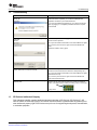
View ........................................................................................................................... 8
Capturing Data ............................................................................................................... 9
5.1
Setup ................................................................................................................. 9
5.2
Connect to Board ................................................................................................... 9
5.3
Capture Single Batch ............................................................................................. 10
5.4
Continuous Capture ............................................................................................... 10
Import and Export of Data ................................................................................................. 10
6.1
Import Data ......................................................................................................... 10
6.2
Export Data ........................................................................................................ 10
Data Analysis ............................................................................................................... 10
7.1
Analysis Settings .................................................................................................. 10
7.2
Analysis Window Output ......................................................................................... 11
Plot Tools .................................................................................................................... 12
Keyboard Commands ...................................................................................................... 12
MATLAB Interface .......................................................................................................... 13
Results ....................................................................................................................... 13
Troubleshooting ............................................................................................................ 15
SP Devices Intellectual Property ......................................................................................... 15
Printed-Circuit Board Layout, Bill of Materials, and Schematic ...................................................... 16
14.1 Printed-Circuit Board Layout ..................................................................................... 16
14.2 Bill of Materials .................................................................................................... 20
14.3 Schematic .......................................................................................................... 22
List of Figures
1
2
3
4
5
6
Board Layout ................................................................................................................. 4
100-MHz ..................................................................................................................... 13
230-MHz ..................................................................................................................... 13
491.5-MHz................................................................................................................... 14
ADS5474-ADX .............................................................................................................. 14
Layer 1 ....................................................................................................................... 16
SLAU247 – August 2008
Submit Documentation Feedback
ADS5474 ADX Evaluation Board for Interleaving
1
www.ti.com
7
8
9
10
11
12
13
14
15
16
17
18
Layer 2 .......................................................................................................................
Layer 3 .......................................................................................................................
Layer 4 .......................................................................................................................
Layer 5 .......................................................................................................................
Layer 6 .......................................................................................................................
Layer 7 .......................................................................................................................
Layer 8 .......................................................................................................................
Front End Schematic ......................................................................................................
FPGA I/O Schematic .......................................................................................................
USB and Logic Analyzer Connectors ....................................................................................
FPGA System Schematic .................................................................................................
Power Supply Schematic ..................................................................................................
17
17
18
18
19
19
20
22
23
24
25
26
List of Tables
1
2
3
4
DIP Switches Functional Descriptions .................................................................................... 5
DIP Switches Modes ........................................................................................................ 5
LED Functions................................................................................................................ 5
Bill of Materials ............................................................................................................. 20
MATLAB is a trademark of The MathWorks, Inc.
2
ADS5474 ADX Evaluation Board for Interleaving
SLAU247 – August 2008
Submit Documentation Feedback
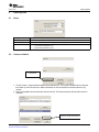
Overview
www.ti.com
1
Overview
This user’s guide gives a general overview of the ADS-ADX Evaluation Board for interleaving (later called
ADS-ADX EVM). It provides a description of the features and functions to consider when using the
module.
1.1
Purpose
The ADS-ADX EVM provides a platform for evaluating two interleaved ADS5474 analog-to-digital
converters (ADC) with a combined sampling rate of 800 MSPS. The ADS5474 is a 14-bit, 400-MSPS ADC
which is pinout compatible with the ADS5463, a 12-bit, 500-MSPS ADC. For a more in-depth theoretical
description of ADC interleaving, consult the white paper Frequency-Response Mismatch Errors and Digital
Correction in Time-Interleaved ADCs – available at www.spdevices.com. For system design with this
technology, consult the SP Devices application note Recommended Analog Front-End Design for ADX
with ADS5474/ADS5463. The ADS-ADX EVM contains an ADC interleaving IP core from SP Devices. For
commercial information and available platforms, contact SP Devices.
1.2
EVM Basic Functions
One analog input into the EVM is provided via the SMA connector. The input is AC-coupled, and the user
supplies a single-ended input signal, which is converted into a differential signal at the input. The
ADS-ADX EVM provides an SMA connector for input of the ADC clock. The external clocking interface is
to be clocked with a 50% duty cycle clock, at half of the sampling rate of the interleaved system sampling
rate.
The interleaving and digital post-correction (ADX IP-core) is implemented in real time using the Virtex-5
FPGA on the board.
Digital output from the EVM is provided both by two Soft Touch Probe (support for Agilent E5405A and
Tektronix P6908 probes) connectors for logic analyzers and by a USB connector for connecting a
personal computer. The USB interface samples the data into internal FPGA memory, which has a
maximum depth of 65,536 samples.
1.3
Power Requirements
The ADS-ADX EVM is powered through the 6-Vdc power supply adapter that is supplied. Power
consumption during operation is approximately 12 W for the board.
1.4
ADS-ADX EVM Operational Procedure
1.
2.
3.
4.
Verify the DIP switch settings to reflect your intended setup (Section 2.5 and Table 2)
Connect the supply power to the EVM, from the supplied mains adapter.
Press the reset button.
Use a 50-Ω function generator with an output swing of ±1 V at the clocking speed of half the full
system, with a duty cycle of 50% (±3%).
5. Connect a 50-Ω function generator with a 55-MHz, 0-V offset, 700-mV amplitude sine wave to the input
of the ADC channel.
6. The digital output pattern on the Soft Touch Probe connector now represents a sine wave and can be
monitored with a logic analyzer.
7. Or connect a USB cable between the board and your computer, start the program ADCaptureLab
(installation: see section Software), and collect the data. The plots provided are a time-series plot and
an FFT of the signal.
SLAU247 – August 2008
Submit Documentation Feedback
ADS5474 ADX Evaluation Board for Interleaving
3
Circuit and Operational Description
www.ti.com
2
Circuit and Operational Description
2.1
Schematic Diagram
Figure 1. Board Layout
2.2
Power
Power is supplied via the 6-Vdc external power supply which is then distributed onboard using several
voltage regulators.
2.3
Clock Input
A single-ended sinusoidal clock with a 50% (±3%) duty cycle must be applied to the SMA clock input, J10.
The output swing of the clock must be ±1 V. The clock frequency must not exceed 400 MSPS for the
ADS5474. The single-ended clock input is converted into a differential signal by using a transformer. The
0° phase output of the transformer is used to clock ADC1 whereas the 180° phase output is used to clock
ADC2.
2.4
Analog Input
A single-ended analog input must be applied to the SMA analog input, J9. The amplitude of the signal
must not exceed 2.2-Vpp differential at the input of the ADCs. The analog input is converted into a
differential signal by using a transformer and is fed to both ADCs. When providing an analog input,
consider the following guidelines for correct operation of the ADX IP core when enabled.
1. The analog input must be less the 85% of the Nyquist band. The Nyquist band refers to one-half of the
combined interleaved sampling rate of the analog input signal.
2. On initial power up, the analog input must be greater than 7.5% of the Nyquist band for correct
estimation to occur. After estimation has occurred, one can put analog input signals representing less
then 7.5% of the Nyquist band.
3. For single- tone analysis only, users cannot input a tone of FS/4 and have adequate correction of the
interleaved tone. In this case, the interleaved spur falls on top of the wanted single tone, which cannot
be distinguished by the ADX algorithm. FS refers to the combined sampling rate of the analog input.
4
ADS5474 ADX Evaluation Board for Interleaving
SLAU247 – August 2008
Submit Documentation Feedback
Circuit and Operational Description
www.ti.com
2.5
DIP Switches
The DIP switch ramp on the board has the following control possibilities:
Table 1. DIP Switches Functional Descriptions
DIPs
[XXXXXX]
[123456]
Functional Description
1
Reserved. Set to zero.
2
Reserved. Set to zero.
3
Reserved. Set to zero.
4
Nyquist band selector [0 = first Nyquist band, 1 = second Nyquist band]
5
Switch for raw or post-processed interleaved output.
[0 = raw interleaved data, 1 = post-processed data]
6
ADC power down. [0 = ADC Power down, 1 = ADC Power on].
Table 2. DIP Switches Modes
DIPs
[XXXXXX]
[123456]
2.6
2.6.1
Example of Configurations
(X is undefined. 0 is down, towards the numbers of the DIP ramp)
[000X01]
The output from the ADS-ADX EVM is raw interleaved data.
[000011]
The output from the ADS-ADX EVM is the post-processed interleaved data.
The signal is reconstructed for the first Nyquist band.
[000111]
The output from the ADS-ADX EVM is the post-processed interleaved data.
The signal is reconstructed for the second Nyquist band.
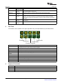
Onboard Status Output
LEDs
Four LEDs are on the board. A more thorough description on the signal requirements for estimation is
available in the data sheet for the ADX IP-core.
Table 3. LED Functions
LED
Color
Description
D4
Green
On – Channel mismatch has been estimated and outputs are valid to specification.
Off – Channel mismatch is not estimated, output may be outside specification.
Blink (together with D2) – Clock is not stable or not connected
D3
Green
On – A valid calibration signal is available and the post-processing tracks the channel mismatch.
Off – A valid calibration signal is not available and the post-processing is locked to last estimated channel
mismatch.
Blink (together with D1) – Clock is not stable or not connected
D2
Red
On – License checked and is OK.
Off – License not yet checked.
Slow blink – License time expired. Reset manually to renew.
Fast blink – License error.
D1
Red
On – New available dataset is stored in internal memory.
Off – No new dataset is available.
(This LED will blink when in continuous acquisition mode).
SLAU247 – August 2008
Submit Documentation Feedback
ADS5474 ADX Evaluation Board for Interleaving
5
Installation
2.7
2.7.1
www.ti.com
Digital Outputs
Soft Touch Probe Connector
On the board are two soft touch probe connectors that output the data, as configured by the DIP switches.
2.7.2
USB Connector
The onboard USB1.1 chip communicates with the FPGA. Transfer speed is 3 megabaud.
3
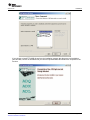
Installation
To install the software, run the ADCaptureLab-setup.exe file and follow the instructions for installation.
Before continuing, you need to close any other application running to avoid the need of rebooting the
system.
6
ADS5474 ADX Evaluation Board for Interleaving
SLAU247 – August 2008
Submit Documentation Feedback
www.ti.com
Installation
If you choose to install FTDI USB drivers from the installation program, the drivers are pre-installed on
your hard disk, but are not activated until you connect a powered ADS-ADX EVM to the computer for the
first time.
SLAU247 – August 2008
Submit Documentation Feedback
ADS5474 ADX Evaluation Board for Interleaving
7
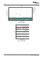
View
4
www.ti.com
View
SETTINGS/SETUP
(5.1)
Plot settings (7.1)
Time-series plot of
data
FFT plot
Connect & Capture (5.2)
Import & Export
Plot tools (8)
Analysis window
(7.2)
8
ADS5474 ADX Evaluation Board for Interleaving
SLAU247 – August 2008
Submit Documentation Feedback
Capturing Data
www.ti.com
5
Capturing Data
5.1
Setup
5.2
Setting
Description
Sample frequency
Set the sampling frequency for the system.
Input frequency
Set the input frequency. Only used for tagging when exporting data.
Board
Available choices:
• [1] ADX EVM 2xADS5463 (12b)
• [2] ADX EVM 2xADS5474 (14b)
Connect to Board
Find board
1. To find a board – push the button labeled Find USB Devices. The boards connected to the computer
then show up in the Devices box. Status information on the enumeration of devices shows in Log
window.
2. Select a compatible device board from the Devices list. The buttons Acquire data and Run are then
activated.
Acquire single batch data
SLAU247 – August 2008
Submit Documentation Feedback
ADS5474 ADX Evaluation Board for Interleaving
9
Import and Export of Data
5.3
www.ti.com
Capture Single Batch
To capture a single batch from the board, press Acquire Data.
5.4
Continuous Capture
To capture continuously, pressing the Run. button changes name to Stop, and pressing it stops the
capturing. If plots are in Play mode (see Section 7), plots are updated continuously as new data arrives
from the board.
Run/Stop button for continuous capture
6
Import and Export of Data
6.1
Import Data
Select a file (file on text file format supported) in dialog box, and press Open. File contents are loaded into
the plot windows (unless they are in Pause mode). To import, you can also drag and drop the file to the
ADCaptureLab main window directly.
6.2
Export Data
Select filename in dialog box, and press Save. Data can be exported on a text file format with a header, or
a pure ASCII file for use with MATLAB™, for example.
7
Data Analysis
7.1
Analysis Settings
7.1.1
Type of Analysis
Analysis type
10
ADS5474 ADX Evaluation Board for Interleaving
SLAU247 – August 2008
Submit Documentation Feedback
Data Analysis
www.ti.com
Analysis Type
Description
Single-tone test
Supports analysis of code range, fundamental, harmonics, SFDR, SNDR (ENOB), interleaving errors (image
and offset spur).
Two-tone test
Supports analysis of code range, fundamentals, SFDR, SNDR (ENOB), interleaving errors.
Other tests
Supports analysis of code range only.
7.1.2
Nyquist Zone Settings
Nyquist Zone (1)
Description
Nyquist zone 1
Input signal frequencies in Nyquist zone 1. { 0.0 < fin < fs/2 }. Fs refers to the combined interleaved sampling
rate of the analog input signal.
Nyquist zone 2
Input signal frequencies in Nyquist zone 2. {fs/2 < fin < fs }. Fs refers to the combined interleaved sampling rate
of the analog input signal.
(1)
7.1.3
Check that board is configured for the Nyquist zone selected, when evaluating performance
View Settings
Setting
Description
Color scheme
Sets the color scheme of the plot routines. Available modes are:
Window
7.2
•
White background (printer-friendly)
•
Black background
Windowing function used for FFT and for analysis functions. Available:
•
Blackman
•
Hamming
•
Rectangular
Autoscale FFT Y-Axis
When enabled, autoscales the y-axis of the FFT plot. If disabled, y-axis is locked between 0 and –130
dBFS.
Mark signal props
When enabled, fundamental tone(s) and SFDR limiter are marked in FFT.
Mark harmonics
When enabled, harmonics (second–seventh) are marked in FFT. Supported for single-tone tests only.
Mark interleaving
When enabled, interleaving errors are marked in FFT. Supported for single-tone tests and two-tone tests
only.
Analysis Window Output
Analysis Item
Valid for
Description
Analysis Type(s)
Codes
All
Code range read in batch and length of batch read.
DC Power
All
DC power in dBFS.
Fundamental
tone(s)
Single-tone
Two-tone
Identified fundamental tones (power and frequency)
Power maximum
Other
Identified power maximum (power and frequency)
SLAU247 – August 2008
Submit Documentation Feedback
ADS5474 ADX Evaluation Board for Interleaving
11
Plot Tools
8
www.ti.com
Analysis Item
Valid for
Description
Analysis Type(s)
Image spur(s)
Single-tone
Two-tone
Interleaving image spurs caused by gain mismatch and aperture time delay mismatch of
the channels (power and frequency)
Offset spur
Single-tone
Two-tone
Interleaving offset spur caused by offset mismatch of the channels (power)
SFDR
Single.-tone
Two-tone
Spurious-Free Dynamic Range. Power relation between fundamental tone and largest
distortion. For a two-tone test, this is calculated as the relation between the largest
fundamental tone and the largest distortion. Frequency position of limiting component is
calculated.
SNDR
Single-tone
Two-tone
Signal-to-Noise and Distortion Ratio. Power relation between fundamental tone and noise
and distortion.
ENOB
Single-tone
Two-tone
Effective Number Of Bits. Based directly on the SNDR value.
Plot Tools
If the mouse cursor is placed in the upper right side of any of the plot windows, a plot toolbar shows.
Zoom redo
Zoom in
Zoom out
Zoom undo
Zoom to original
9
Plot tool
Description
Play/Pause
To put plot in Play/Pause mode. In play mode, plot displays new data as it arrives either by acquiring or
by importing from file. In pause mode, plot does not update.
Copy
Copies plot window to clipboard
Print
Prints plot window to printer
Save
Exports plot window to bitmap or jpeg image file.
Edit cursors and
markers
Edits the cursors and markers of the plot window
Zoom in
Zooms in
Zoom out
Zooms out
Zoom to original
Zooms to the original setting
Zoom undo
Returns to last zoom setting
Zoom redo
Returns to zoom setting before undo press
Keyboard Commands
Key
12
Description
F1
Show version information for ADCaptureLab software
F2
Show version information for FPGA firmware and FPGA firmware status
F5
Refresh plots
ADS5474 ADX Evaluation Board for Interleaving
SLAU247 – August 2008
Submit Documentation Feedback
MATLAB Interface
www.ti.com
10
MATLAB Interface
Also supplied is a simple MATLAB interface to the evaluation board. It consists of an engine
communicating with the board and returning the data vector on call. The calling syntax is:
11
Initialize:
acquiredata(‘find’)
Acquire data:
data = acquiredata(‘acquire’)
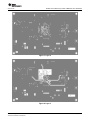
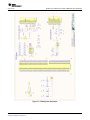
Results
The following typical results were taken from the ADS-ADX evaluation module, using a filtered Agilent
8644B clock source, which provided each ADC a 400-MHz sampling clock. When using the onboard ADX
interleaving technology, this results in a combined 800-MSPS sampling rate of the analog input signal.
Another filtered Agilent 8644B was used to provide a -1-dBFS single tone into the EVM. The results are
displayed in Figure 2 through Figure 5.
Amplitude - dBFS
FFT
f - Frequency - MHz
Figure 2. 100-MHz
Amplitude - dBFS
FFT
f - Frequency - MHz
Figure 3. 230-MHz
SLAU247 – August 2008
Submit Documentation Feedback
ADS5474 ADX Evaluation Board for Interleaving
13
Results
www.ti.com
Amplitude - dBFS
FFT
f - Frequency - MHz
Figure 4. 491.5-MHz
120
Image
Offset
100
dBc
80
SFDR
60
40
20
0
50 60 70 80 90 100 130 170 230 250 270 491 650
f - Frequency - Hz
Figure 5. ADS5474-ADX
14
ADS5474 ADX Evaluation Board for Interleaving
SLAU247 – August 2008
Submit Documentation Feedback
Troubleshooting
www.ti.com
12
Troubleshooting
Problem
Remedy
GUI warns for not installed or activated FTDI Drivers when
starting the
application.
If you did not select to pre-install FTDI Drivers during installation,
install FTDI Drivers separately or re-install the ADCaptureLab
application and select to pre-install FTDI drivers.
If you have pre-installed the FTDI Drivers, you need to activate the
driver by plugging in a compatible powered board to the computer
over the USB.
No devices are found when scanning the USB by pressing
Find USB
Devices
Check if a compatible board is plugged in via USB.
Check if board is powered.
Try to push the onboard reset button. Press Find USB Devices again.
Try to turn the power off and on again. Press Find USB Devices
again.
Restart the software, and try again.
Board is connected and found in list, but when trying to
acquire board does not respond correctly.
Check if board is powered.
Check that correct board format is selected in Setup Settings (5.1).
Try to push the onboard reset button. Press Find USB Devices again,
select board and retry.
Try to turn the power off and on again. Press Find USB Devices
again, select board and retry.
Time series plot or FFT does not update when acquiring or
importing data
The plot which is not updating may be in Pause mode. Put the mouse
cursor in the top right of the plot window in question to enable the
toolbar. If the play symbol is visible (see inset), push it to set the plot
in Play mode.
13
SP Devices Intellectual Property
This evaluation board/kit contains intellectual property belonging to SP Devices, (SP Devices IP). SP
Devices retains all ownership rights in SP Devices IP and no license is granted under any patent right or
other intellectual property right of SP Devices except for use for engineering development, demonstration,
or evaluation purposes.
SLAU247 – August 2008
Submit Documentation Feedback
ADS5474 ADX Evaluation Board for Interleaving
15
Printed-Circuit Board Layout, Bill of Materials, and Schematic
14
www.ti.com
Printed-Circuit Board Layout, Bill of Materials, and Schematic
14.1 Printed-Circuit Board Layout
The following illustrations show the eight layers of the ADX evaluation board.
Figure 6. Layer 1
16
ADS5474 ADX Evaluation Board for Interleaving
SLAU247 – August 2008
Submit Documentation Feedback
www.ti.com
Printed-Circuit Board Layout, Bill of Materials, and Schematic
Figure 7. Layer 2
Figure 8. Layer 3
SLAU247 – August 2008
Submit Documentation Feedback
ADS5474 ADX Evaluation Board for Interleaving
17
Printed-Circuit Board Layout, Bill of Materials, and Schematic
www.ti.com
Figure 9. Layer 4
Figure 10. Layer 5
18
ADS5474 ADX Evaluation Board for Interleaving
SLAU247 – August 2008
Submit Documentation Feedback
www.ti.com
Printed-Circuit Board Layout, Bill of Materials, and Schematic
Figure 11. Layer 6
Figure 12. Layer 7
SLAU247 – August 2008
Submit Documentation Feedback
ADS5474 ADX Evaluation Board for Interleaving
19
Printed-Circuit Board Layout, Bill of Materials, and Schematic
www.ti.com
Figure 13. Layer 8
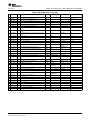
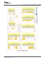
14.2 Bill of Materials
Table 4. Bill of Materials
Qt
y
Internal No.
4
2
Description
Package
100-000-025
Resistor, 10 Ω, 0402, 1%, 0.063W
0402
R96–R99
100-000-033
Resistor, 22 Ω, 0402, 1%, 0.063W
0402
R42, R44
2
100-000-039
Resistor, 39 Ω, 0402, 1%, 0.063W
0402
R61, R62
1
100-000-041
Resistor, 47 Ω, 0402, 1%, 0.063W
0402
R120
2
100-000-049
Resistor, 100 Ω, 0402, 1%, 0.063W
0402
R110, R111
1
100-000-061
Resistor, 330 Ω, 0402, 1%, 0.063W
0402
R123
1
100-000-073
Resistor, 1 kΩ, 0402, 1%, 0.063W
0402
R49
17
100-000-089
Resistor, 4.7 kΩ, 0402, 1%, 0.063W
0402
R22–R27, R34–R37, R39,
R40, R65, R121, R122,
R124, R125
1
100-000-097
Resistor, 10 kΩ, 0402, 1%, 0.063W
0402
R43
0
100-001-043
Resistor, 56 Ω, 0603, 1%, 0.1W
0603
4
100-001-047
Resistor, 82 Ω, 0603, 1%, 0.1W
0603
R30–R33
1
100-001-069
Resistor, 680 Ω, 0603, 1%, 0.1W
0603
R100
1
100-001-083
Resistor, 2.7 kΩ, 0603, 1%, 0.1W
0603
R28
1
100-001-091
Resistor, 5.6 kΩ, 0603, 1%, 0.1W
0603
R41
1
100-001-093
Resistor, 6.8 kΩ, 0603, 1%, 0.1W
0603
R69
1
100-001-095
Resistor, 8.2 kΩ, 0603, 1%, 0.1W
0603
R72
1
100-001-103
Resistor, 18 kΩ, 0603, 1%, 0.1W
0603
R93
2
101-000-000
Capacitor, 1 pF ±0.25pF, 0402, C0G, 50V
0402
C13, C14
2
101-001-019
Capacitor, 10 nF, 10%, 0402, X7R, 25V
0402
C44, C186
84
101-001-022
Capacitor, 100 nF, 10%, 0402, X7R, 16V
0402
C1–C12, C22–C33, C49,
C50, C53, C54, C73–C85,
C87–C92, C103,
C123–C125, C135–C152,
C154–C157, C160–C162,
C190–C197
20
Rev
ADS5474 ADX Evaluation Board for Interleaving
Manufacturer
Manufacturer Part No.
Designators
SLAU247 – August 2008
Submit Documentation Feedback
Printed-Circuit Board Layout, Bill of Materials, and Schematic
www.ti.com
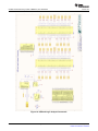
Table 4. Bill of Materials (continued)
Qt
y
Internal No.
2
2
Rev
Description
Package
Manufacturer
Manufacturer Part No.
Designators
101-001-101
Capacitor, 1 µF, 20%, 0402, X5R, 6.3V
0402
C188, C189
101-003-003
Capacitor, 100 nF, 10%, 0603, X7R, 16V
0603
C184, C185
1
101-003-004
Capacitor, 220 nF, 10%, 0603, X7R, 16V
0603
C51
2
101-003-006
Capacitor, 1 µF, 10%, 0603, X5R, 25V
0603
C59, C187
4
101-003-007
Capacitor, 2.2 µF, 10%, 0603, X5R, 16V
0603
2
101-005-000
Capacitor, 100 µF, 20%, 1210, X5R, 6.3V
1210
Taiyo Yuden
JMK325BJ107MY-T
C66, C183
5
101-100-000
Electrolytic capacitor, 100 µF, 0.39 Ω, 20%, 25V, C6, 105°,
CE-KX
C6
Sanyo
16CE100KX
C46, C58, C61, C69, C70
1
101-100-001
Electrolytic capacitor, 100 µF, 0.3 Ω, 20%, 25V, C8, 105°,
CE-KX
C8
Sanyo
25CE100KX
C182
1
101-100-002
Electrolytic capacitor, 330 µF, 0.15 Ω, 20%, 25V, E10, 105°,
CE-KX
E10
Sanyo
25CE330KX
C64
2
102-002-001
Ferrite bead
SMD
FerroxCube
1
102-300-000
0.4–800 MHz transformer, 1:1 impedance ratio
CD542
Mini Circuits
ADT1-1WT+
TR2
2
102-300-002
1:1 transformer (TycoElectronics)
SM-22
Tyco/Macom
ETC1-1-13
TR1, TR3
2
103-002-000
Green LED, 16mcd, 0603
0603
Everlight
EL19-21SYGC
D3, D4
2
103-002-001
Red LED, 19mcd, 0603
0603
Everlight
EL19-21SDRC
D1, D2
1
103-004-001
XC5VSX50T-1FFG665C, Virtex 5 FPGA
BGA
FF665
Xilinx
XC5VSX50T1FFG665C
U3
1
103-005-000
AT45DB321D, 32 Mbit FPGA config memory
SO8W
Atmel
AT45DB321D-SU
U5
1
103-005-002
DS2432, 1-kbit protected 1-wire EEPROM with SHA-1
engine
TSOC8
Maxim
DS2432
U20
2
103-010-014
PTH08080W, 2.2A DC/DC module, 4.5-18V in, 0.9-5.5V out
SMD
Texas Instruments
PTH08080WAZ
U10, U11
1
103-010-016
REG104GA-3.3G4, 3.3V LDO, 1A max, 480mV drop
SOT223-6
Texas Instruments
REG104GA-3.3
U9
1
103-010-017
REG104FA-5, 5V LDO, 1A max, 580mV drop
DDPAK-5
Texas Instruments
REG104FA-5
U14
1
103-010-018
PTH08T230WAZ, 6A DC/DC module, 4.5-14V in, 0.7-5.5V
out
SMD
Texas Instruments
PTH08T230WAZ
U13
2
103-012-002
ADS5474, 14-bit 400 MSPS ADC
PPQFP80
Texas Instruments
ADS5474IPFP
ADC1, ADC2
1
103-014-005
CFPS-32, 50 MHz crystal oscillator 2.5V
SMD7x5
C-MAC
CFPS-32IB 50.0MHz
U4
1
103-015-000
FT232RQ, USB 1.1 serial port
QFN32
FTDI chip
FT232RQ
U6
2
103-016-000
LM809M3-3-08, 3.3V reset circuit
SOT23-3
National
Semiconductor
LM809M3-3.08
U17, U18
0
104-000-001
Pinless connector for Agilent logic analyzers
SMD
Agilent
E5405A
2
104-001-000
SMA connector, 90-degree angle
PTH
Johnson Components
142-0701-551
1
104-001-002
USB type B mini, pth
PTH
1
104-001-005
Power connector 2.0 mm pin , hole mounted
PTH
CLIFF ELECTRONIC
COMPONENTS
DC10A
1
104-001-006
Pin header, 2x7, 2.0 mm spacing
PTH
Molex
0
105-001-000
Fiducial, 3 mm
0
105-001-001
Fiducial, 2 mm
0
105-001-002
Mounting hole, 3,5 mm
0
105-001-003
SP Devices logo
0
105-001-005
1
106-000-004
1
107-000-000
SMD Pushbutton, Alps SKHUAD
ALPS
1
107-000-001
DIP-switch, 6PST
Taiway
C55, C56, C60, C62
L3, L4
J9, J10
J8
J12
J5
TI logo
B
PCB, ADS54xx-ADS-ADX EVM
SLAU247 – August 2008
Submit Documentation Feedback
PCB1
PB1
DM-06
SW1
ADS5474 ADX Evaluation Board for Interleaving
21
Printed-Circuit Board Layout, Bill of Materials, and Schematic
www.ti.com
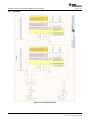
14.3 Schematic
Figure 14. Front End Schematic
22
ADS5474 ADX Evaluation Board for Interleaving
SLAU247 – August 2008
Submit Documentation Feedback
www.ti.com
Printed-Circuit Board Layout, Bill of Materials, and Schematic
Figure 15. FPGA I/O Schematic
SLAU247 – August 2008
Submit Documentation Feedback
ADS5474 ADX Evaluation Board for Interleaving
23
Printed-Circuit Board Layout, Bill of Materials, and Schematic
www.ti.com
Figure 16. USB and Logic Analyzer Connectors
24
ADS5474 ADX Evaluation Board for Interleaving
SLAU247 – August 2008
Submit Documentation Feedback
www.ti.com
Printed-Circuit Board Layout, Bill of Materials, and Schematic
Figure 17. FPGA System Schematic
SLAU247 – August 2008
Submit Documentation Feedback
ADS5474 ADX Evaluation Board for Interleaving
25
Printed-Circuit Board Layout, Bill of Materials, and Schematic
www.ti.com
Figure 18. Power Supply Schematic
26
ADS5474 ADX Evaluation Board for Interleaving
SLAU247 – August 2008
Submit Documentation Feedback
EVALUATION BOARD/KIT IMPORTANT NOTICE
Texas Instruments (TI) provides the enclosed product(s) under the following conditions:
This evaluation board/kit is intended for use for ENGINEERING DEVELOPMENT, DEMONSTRATION, OR EVALUATION PURPOSES
ONLY and is not considered by TI to be a finished end-product fit for general consumer use. Persons handling the product(s) must have
electronics training and observe good engineering practice standards. As such, the goods being provided are not intended to be complete
in terms of required design-, marketing-, and/or manufacturing-related protective considerations, including product safety and environmental
measures typically found in end products that incorporate such semiconductor components or circuit boards. This evaluation board/kit does
not fall within the scope of the European Union directives regarding electromagnetic compatibility, restricted substances (RoHS), recycling
(WEEE), FCC, CE or UL, and therefore may not meet the technical requirements of these directives or other related directives.
Should this evaluation board/kit not meet the specifications indicated in the User’s Guide, the board/kit may be returned within 30 days from
the date of delivery for a full refund. THE FOREGOING WARRANTY IS THE EXCLUSIVE WARRANTY MADE BY SELLER TO BUYER
AND IS IN LIEU OF ALL OTHER WARRANTIES, EXPRESSED, IMPLIED, OR STATUTORY, INCLUDING ANY WARRANTY OF
MERCHANTABILITY OR FITNESS FOR ANY PARTICULAR PURPOSE.
The user assumes all responsibility and liability for proper and safe handling of the goods. Further, the user indemnifies TI from all claims
arising from the handling or use of the goods. Due to the open construction of the product, it is the user’s responsibility to take any and all
appropriate precautions with regard to electrostatic discharge.
EXCEPT TO THE EXTENT OF THE INDEMNITY SET FORTH ABOVE, NEITHER PARTY SHALL BE LIABLE TO THE OTHER FOR ANY
INDIRECT, SPECIAL, INCIDENTAL, OR CONSEQUENTIAL DAMAGES.
TI currently deals with a variety of customers for products, and therefore our arrangement with the user is not exclusive.
TI assumes no liability for applications assistance, customer product design, software performance, or infringement of patents or
services described herein.
Please read the User’s Guide and, specifically, the Warnings and Restrictions notice in the User’s Guide prior to handling the product. This
notice contains important safety information about temperatures and voltages. For additional information on TI’s environmental and/or
safety programs, please contact the TI application engineer or visit www.ti.com/esh.
No license is granted under any patent right or other intellectual property right of TI covering or relating to any machine, process, or
combination in which such TI products or services might be or are used.
FCC Warning
This evaluation board/kit is intended for use for ENGINEERING DEVELOPMENT, DEMONSTRATION, OR EVALUATION PURPOSES
ONLY and is not considered by TI to be a finished end-product fit for general consumer use. It generates, uses, and can radiate radio
frequency energy and has not been tested for compliance with the limits of computing devices pursuant to part 15 of FCC rules, which are
designed to provide reasonable protection against radio frequency interference. Operation of this equipment in other environments may
cause interference with radio communications, in which case the user at his own expense will be required to take whatever measures may
be required to correct this interference.
EVM WARNINGS AND RESTRICTIONS
It is important to operate this EVM within the input voltage range of 5.7 V to 6.5 V and the output voltage range of 5.7 V to 6.5 V.
Exceeding the specified input range may cause unexpected operation and/or irreversible damage to the EVM. If there are questions
concerning the input range, please contact a TI field representative prior to connecting the input power.
Applying loads outside of the specified output range may result in unintended operation and/or possible permanent damage to the EVM.
Please consult the EVM User's Guide prior to connecting any load to the EVM output. If there is uncertainty as to the load specification,
please contact a TI field representative.
During normal operation, some circuit components may have case temperatures greater than 25°C. The EVM is designed to operate
properly with certain components above 50°C as long as the input and output ranges are maintained. These components include but are
not limited to linear regulators, switching transistors, pass transistors, and current sense resistors. These types of devices can be identified
using the EVM schematic located in the EVM User's Guide. When placing measurement probes near these devices during operation,
please be aware that these devices may be very warm to the touch.
Mailing Address: Texas Instruments, Post Office Box 655303, Dallas, Texas 75265
Copyright © 2008, Texas Instruments Incorporated
IMPORTANT NOTICE
Texas Instruments Incorporated and its subsidiaries (TI) reserve the right to make corrections, modifications, enhancements, improvements,
and other changes to its products and services at any time and to discontinue any product or service without notice. Customers should
obtain the latest relevant information before placing orders and should verify that such information is current and complete. All products are
sold subject to TI’s terms and conditions of sale supplied at the time of order acknowledgment.
TI warrants performance of its hardware products to the specifications applicable at the time of sale in accordance with TI’s standard
warranty. Testing and other quality control techniques are used to the extent TI deems necessary to support this warranty. Except where
mandated by government requirements, testing of all parameters of each product is not necessarily performed.
TI assumes no liability for applications assistance or customer product design. Customers are responsible for their products and
applications using TI components. To minimize the risks associated with customer products and applications, customers should provide
adequate design and operating safeguards.
TI does not warrant or represent that any license, either express or implied, is granted under any TI patent right, copyright, mask work right,
or other TI intellectual property right relating to any combination, machine, or process in which TI products or services are used. Information
published by TI regarding third-party products or services does not constitute a license from TI to use such products or services or a
warranty or endorsement thereof. Use of such information may require a license from a third party under the patents or other intellectual
property of the third party, or a license from TI under the patents or other intellectual property of TI.
Reproduction of TI information in TI data books or data sheets is permissible only if reproduction is without alteration and is accompanied
by all associated warranties, conditions, limitations, and notices. Reproduction of this information with alteration is an unfair and deceptive
business practice. TI is not responsible or liable for such altered documentation. Information of third parties may be subject to additional
restrictions.
Resale of TI products or services with statements different from or beyond the parameters stated by TI for that product or service voids all
express and any implied warranties for the associated TI product or service and is an unfair and deceptive business practice. TI is not
responsible or liable for any such statements.
TI products are not authorized for use in safety-critical applications (such as life support) where a failure of the TI product would reasonably
be expected to cause severe personal injury or death, unless officers of the parties have executed an agreement specifically governing
such use. Buyers represent that they have all necessary expertise in the safety and regulatory ramifications of their applications, and
acknowledge and agree that they are solely responsible for all legal, regulatory and safety-related requirements concerning their products
and any use of TI products in such safety-critical applications, notwithstanding any applications-related information or support that may be
provided by TI. Further, Buyers must fully indemnify TI and its representatives against any damages arising out of the use of TI products in
such safety-critical applications.
TI products are neither designed nor intended for use in military/aerospace applications or environments unless the TI products are
specifically designated by TI as military-grade or "enhanced plastic." Only products designated by TI as military-grade meet military
specifications. Buyers acknowledge and agree that any such use of TI products which TI has not designated as military-grade is solely at
the Buyer's risk, and that they are solely responsible for compliance with all legal and regulatory requirements in connection with such use.
TI products are neither designed nor intended for use in automotive applications or environments unless the specific TI products are
designated by TI as compliant with ISO/TS 16949 requirements. Buyers acknowledge and agree that, if they use any non-designated
products in automotive applications, TI will not be responsible for any failure to meet such requirements.
Following are URLs where you can obtain information on other Texas Instruments products and application solutions:
Products
Amplifiers
Data Converters
DSP
Clocks and Timers
Interface
Logic
Power Mgmt
Microcontrollers
RFID
RF/IF and ZigBee® Solutions
amplifier.ti.com
dataconverter.ti.com
dsp.ti.com
www.ti.com/clocks
interface.ti.com
logic.ti.com
power.ti.com
microcontroller.ti.com
www.ti-rfid.com
www.ti.com/lprf
Applications
Audio
Automotive
Broadband
Digital Control
Medical
Military
Optical Networking
Security
Telephony
Video & Imaging
Wireless
www.ti.com/audio
www.ti.com/automotive
www.ti.com/broadband
www.ti.com/digitalcontrol
www.ti.com/medical
www.ti.com/military
www.ti.com/opticalnetwork
www.ti.com/security
www.ti.com/telephony
www.ti.com/video
www.ti.com/wireless
Mailing Address: Texas Instruments, Post Office Box 655303, Dallas, Texas 75265
Copyright © 2008, Texas Instruments Incorporated