1
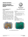
Si53301/4-EVB
Table 1. JP2, JP3, JP4, and JP5 Output Signal Format
SFOUTX11
SFOUTX01
VDDOX = 3.3 V
VDDOX = 2.5 V
VDDOX = 1.8 V
Open2
Open2
LVPECL
LVPECL
N/A
Ground
Ground
LVDS
LVDS
LVDS
Ground
VDD
LVCMOS, 24 mA drive
LVCMOS, 18 mA drive
LVCMOS, 12 mA drive
VDD
Ground
LVCMOS, 18 mA drive
LVCMOS, 12 mA drive
LVCMOS, 9 mA drive
VDD
VDD
LVCMOS, 12 mA drive
LVCMOS, 9 mA drive
LVCMOS, 6 mA drive
Open2
Ground
LVCMOS, 6 mA drive
LVCMOS, 4 mA drive
LVCMOS, 2 mA drive
Open2
VDD
LVPECL Low power
LVPECL Low power
N/A
Ground
Open2
CML
CML
CML
VDD
Open2
HCSL
HCSL
HCSL
Notes:
1. Ground means short center pin to ground pin. VDD means short center pin to VDD pin.
Open means leave center pin open.
2. SFOUTX are three-level input pins.
Table 2. Jumper Selections for JP1,6
Signal*
Jumper
Si53301
Si53304
Jumper Position
Jumper Position
Ground
Open
VDD
Ground
Open
VDD
DIVA(OE1)
JP1
/2
/1
/4
Q1 Disabled Q1 Enabled
Q1 Enabled
DIVB(OE5)
JP6
/2
/1
/4
Q5 Disabled Q5 Enabled
Q5 Enabled
*Note: The signal name in parentheses applies to the Si53304 device, which is not installed from the factory.
Table 3. Jumper Selections for P3,4,5,6,7
Signal*
Jumper
Si53301
Si53304
Jumper Position
Jumper Position
Shorted
Open
Shorted
Open
CLK_SEL
P3
CLK0 Selected
CLK1 Selected
CLK0 Selected
CLK1 Selected
NC(OE1)
P4
NA
NA
Q1 Disabled
Q1 Enabled
OEA(OE2)
P5
Q0,1,2 Disabled
Q0,1,2 Enabled
Q2 Disabled
Q2 Enabled
OEB(OE3)
P6
Q3,4,5 Disabled
Q3,4,5 Enabled
Q3 Disabled
Q3 Enabled
NC(OE4)
P7
NA
NA
Q4 Disabled
Q4 Enabled
*Note: The signal name in parentheses applies to the Si53304 device, which is not installed from the factory.
Rev. 0.3
3