1
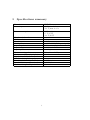
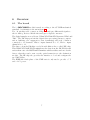
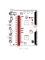
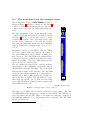
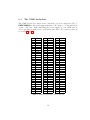
i - trOnics GmbH
Multi-channel Sampling Analogue-to-Digital
Converter Module
i - SADC108032
for the Mainz Crystal Ball Detector
User’s Manual
This manual was written to guide you in the installation, configuration and
operation of the i - SADC108032 multi-channel sampling analogue-to-digital
converter module.
i - trOnics GmbH excludes completely any liability for any indirect, special,
incidental, or consequential damages (including damages for loss of profits,
loss of business, loss of use or data, interruption of business and the like)
even if i - trOnics GmbH has been advised of the possibility of such damages
arising from any defect or error in this manual or product.
Information and specifications in this manual are for informational use only.
They are subject to change at any time without notice, and should not be
construed as a declaration of conformity for this product nor as a commitment
by i - trOnics GmbH. i - trOnics GmbH assumes no responsibility or liability
for any errors or inaccuracies that may appear in this manual, including the
products and software described in it.
October 2003, Rev. 0.96
i - trOnics GmbH
Erikastrasse 18b
D-85521 Hohenbrunn
Germany
Tel:
+49-89-66006899
Fax:
+49-89-66000377
Internet: www.i-tronics.net
Email:
[email protected]
for general information
[email protected] for sales information
c
i - trOnics GmbH. All Rights Reserved
Copyright 2003
Product warranty or service will not be extended if: (i) the product is repaired, modified or altered, unless such repair, modification or alteration is
authorised by i - trOnics; or (ii) the serial number of the product is defaced
or missing.
Products and corporate names appearing in this manual may or may not
be registered trademarks or copyrights of their respective companies, and
are used only for identification or explanation and to the owner’s benefit,
without intent to infringe.
I
Contents
1 FCC statements and CE conformity declaration
1
2 Safety information
2
3 Specifications summary
3
4 Scope of supply
4
5 Hardware installation
5
6 Overview
6.1 The board . . . . . . . . . . . . . . . .
6.2 The front-panel and the analogue input
6.3 The VME backplane . . . . . . . . . .
6.4 Data processing and data flow . . . . .
.
.
.
.
.
.
.
.
.
.
.
.
.
.
.
.
.
.
.
.
.
.
.
.
.
.
.
.
.
.
.
.
.
.
.
.
.
.
.
.
.
.
.
.
.
.
.
.
.
.
.
.
7
7
9
10
11
7 Data format
14
7.1 Decoding the data . . . . . . . . . . . . . . . . . . . . . . . . 15
8 Configuration and loading
18
8.1 Loading the HL FPGA . . . . . . . . . . . . . . . . . . . . . . 18
8.2 Loading the ZR FPGAs . . . . . . . . . . . . . . . . . . . . . 19
8.3 Configuring the ZR FPGAs . . . . . . . . . . . . . . . . . . . 19
II
1
FCC statements and CE conformity declaration
1
2
Safety information
Before starting with the installation of the i - SADC108032 module, please
verify that you received the shipment is complete and in perfect condition.
Do not try to install modules that have visible defects, it could damage other
components.
• Always use insulated, antistatic tools and avoid touching the electronic
components.
• Before using the module in a crate, make sure all cables are connected
correctly and the power cables are not damaged.
• To prevent electrical shock hazard, disconnect the power from the electrical outlet before relocating the system.
• When you add or remove modules from your system, ensure that the
crate is switched off and that the power supply cable is out of the
socket.
• Do not use force when plugging/unplugging modules.
• To avoid short circuits keep small conductive parts like screws, clips,
and staples away from connectors, slots, sockets and circuitry.
• Avoid dust, humidity, and temperature extremes. Do not place the
module in any area where it may become wet.
2
3
Specifications summary
Form-factor
Power inputs
VME 6U
+5 V/max. 5 A
−12 V/max. 0.8 A
Power consumption
35 W total
+5 V/25 W
−12 V/10 W
Number of channels
32
ADC resolution
10 bit
Sampling rate
40 MHz
Noise performance
0.6 LSB RMS (DC input signal)
Input impedance
50 Ω
Input range
-1.25 V to 0.25 V
Input signal connector
2 × 34 pin
Maximum trigger latency
511 cycles = 12.78 µsec
Maximum number of samples/event 128
Depth of multi-hit buffer
4
Number of sample integrals
3
Data bandwidth of optical link
40 MByte/sec
Bandwidth for configuration data
40 MBit/sec
Maximum length of optical fibre
100 m
3
4
Scope of supply
Please check the contents of your package. The scope of supply of a i SADC108032 module includes:
• 1 × i - SADC108032 multi-channel sampling ADC VME 6U board
• 1 × manual
If your package is not complete or is damaged, please contact i - trOnics.
4
5
Hardware installation
Attention:
• Make sure that you are using a standard VME crate with IEEE-1014
back plane.
• Make sure the VME crate has a fan unit which provides sufficient air
cooling. Do not operate the module without active cooling.
• Make sure that unused slots of the VME crate are closed with metal
screens to improve ventilation and electromagnetic emission.
• Always use insulated, antistatic tools and avoid touching the electronic
components.
• Do not install modules with visible defects.
• Do not hot-plug modules.
• Do not use force to insert/remove modules.
• Avoid dust and dirt on the optical fibre connectors. Always use the
protection caps for unconnected plugs and jacks.
• Carefully read the safety information in chapter 2.
Procedure:
1. Switch off the VME crate and pull the power supply cable out of the
socket.
2. Carefully insert the i - SADC108032 module in the VME slot and screw
the front-panel to the crate.
3. Connect the cables for the analogue signals. Pin 1 sits in the lower
right corner of the 34 pin connector (see subsection 6.2).
4. Reconnect the power supply cable and switch on the crate.
5. Make sure that the rightmost FPGA LED on the front-panel is lit (see
subsection 6.2). If this is not the case the PROM for the HL FPGA
has to be loaded (see subsection 8.1).
5
6. Setup and load the i - MUX module to which the i - SADC will be
connected to.
7. Connect the fibre from the i - MUX module to the optical transceiver.
The optical cable used must be crossed so that the transmitter (Tx)
of the i - MUX transceiver is connected with the receiver (Rx) of the
i - SADC module and vice versa.
8. Make sure that the ’Clk’ LED on the front-panel (see subsection 6.2)
is lit to indicate that the optical link was established successfully.
9. Check that the ’Syn’ LED on the front-panel (see subsection 6.2) is
active indicating that the clock recovery chip is active.
10. Load the ZR FPGAs (see subsection 8.2).
11. Set the configuration parameters of the ZR FPGAs (see subsection 8.3).
6
6
6.1
Overview
The board
The i - SADC108032 module is made according to the 6U VME mechanical
standard. A schematic is shown in figure 1.
Two 34 pin flat cable connectors bring the analogue differential signals to
the 32 Analog Devices AD9214-80 analogue-to-digital converters.
The digital samples are read by two Xilinx XC2V1000 FPGAs named ’ZR0’ and
’ZR1’. The ZR chips perform the digital data processing (latency compensation, buffering, zero suppression, data formatting) and each of them is
connected to 16 channels: ZR0 to input channels 0 to 15, ZR1 to input
channels 16 to 31.
The data go from the ZR chips over 16 bit wide links to the so called ’HL’ chip.
This Xilinx XCV100E FPGA multiplexes the data from the ZR FPGAs and
writes them out to the HOTLink Transmitter which serialises and encodes the
data so that they can be sent over the optical transceiver to the destination
module. The HL chip also provides the interface to load and configure the
two ZR FPGAs.
The IEEE-1014 back plane of the VME crate is only used to provide +5 V
and −12 V power.
7
Top side
VME
P1
Clock
recovery
chip
Optical
transceiver
HotLink
transmitter
Xilinx
XC2V1000
Molex
connector
for PROM
programming
ZR
Xilinx
XC18V02VQ44
PROM
Analogue
Input
Ch 31...16
Fuse –12 V
Fuse +5 V
Xilinx
XCV100E
HL
Xilinx
XC2V1000
Analogue
Input
Ch 15...0
ZR
Zero delay
buffers for
clock fan-out
16x
AD9214 ADC
Figure 1: Board schematic
8
VME
P2
6.2
The front-panel and the analogue input
Clk
Syn
Tx
Rx
Com
Ack
I2C
FPGA
Tr Rs FF
CHANNELS 16-31
CHANNELS 0 -15
The front-panel of the i - SADC108032 module is
shown in figure 2 has three connectors: the LCTM1
connector of the optical link and the two flat cable
connectors for the analogue differential input signals.
The pin assignment of the 34 pin input flat cable
connectors and the termination circuitry is shown
in figure 3. If one looks into the connector pin 1
is in the lower right corner. The upmost two pins
33 and 34 are connected to the analogue ground.
The analogue differential input lines are terminated
with 50 Ω and have an input range of −1.25 V to
0.25 V.
Furthermore there are ten LEDs. The two LEDs
above the optical transceiver indicate the status of
the optical link and should be always on during normal operation. The ’Clk’ LED is lit when the fibre
connection with the destination module was established successfully. The ’Syn’ LED indicates that
the clock recovery chip is active.
The two LEDs below the LCTM connector indicate
the activity on the configuration bus that connects
the HL FPGA with the ZR chips. The ’Com’ LED
indicates the activity on the data line. The ’Ack’ LED
shows the successful transmission of data packets.
Further below three LEDs display the loading status of the three FPGAs. The left LED is for the
ZR0 chip, the middle one for ZR1 and the right
one for the HL FPGA. During normal operation all
three LEDs should be lit.
i - SADC
108032.0
Figure 2: Front-panel
Figure 3: Analogue input connector pin-out
The last row of LEDs shows activity relevant for data taking. The left
’Tr’ LED blinks when triggers are coming in. The middle ’Rs’ LED shows
the reset pulses and the ’FF’ LED on the right side indicates overflows in
the multi-hit buffer due to too high trigger and/or data rate. The ’FF’ LED
should be always off.
1
LCTM is a trademark of Lucent
9
6.3
The VME backplane
The VME P1 and P2 connectors are only used for power connections. The i SADC108032 module needs approximately 25 W on the +5 V line and 10 W
on the −12V line. Make sure that the power supply of your VME crate is
able to provide enough power for all inserted modules. For connector pin-out
see tables 1 and 2.
A1
A2
A3
A4
A5
A6
A7
A8
A9
A10
A11
A12
A13
A14
A15
A16
A17
A18
A19
A20
A21
A22
A23
A24
A25
A26
A27
A28
A29
A30
A31
A32
–
–
–
–
–
–
–
–
GND
–
–
–
–
–
–
–
–
–
–
–
–
–
–
–
–
–
–
–
–
–
−12 V
+5 V
B1
B2
B3
B4
B5
B6
B7
B8
B9
B10
B11
B12
B13
B14
B15
B16
B17
B18
B19
B20
B21
B22
B23
B24
B25
B26
B27
B28
B29
B30
B31
B32
–
–
–
–
–
–
–
–
–
–
–
–
–
–
–
–
–
–
–
GND
–
–
GND
–
–
–
–
–
–
–
–
+5 V
C1
C2
C3
C4
C5
C6
C7
C8
C9
C10
C11
C12
C13
C14
C15
C16
C17
C18
C19
C20
C21
C22
C23
C24
C25
C26
C27
C28
C29
C30
C31
C32
–
–
–
–
–
–
–
–
GND
–
–
–
–
–
–
–
–
–
–
–
–
–
–
–
–
–
–
–
–
–
+12 V
+5 V
Table 1: VME backplane P1 connector pin-out
10
A1
A2
A3
A4
A5
A6
A7
A8
A9
A10
A11
A12
A13
A14
A15
A16
A17
A18
A19
A20
A21
A22
A23
A24
A25
A26
A27
A28
A29
A30
A31
A32
reserved
reserved
–
reserved
reserved
reserved
reserved
reserved
reserved
reserved
reserved
reserved
reserved
reserved
reserved
reserved
reserved
reserved
reserved
reserved
reserved
reserved
GND
reserved
GND
reserved
GND
reserved
GND
reserved
reserved
reserved
B1
B2
B3
B4
B5
B6
B7
B8
B9
B10
B11
B12
B13
B14
B15
B16
B17
B18
B19
B20
B21
B22
B23
B24
B25
B26
B27
B28
B29
B30
B31
B32
+5 V
GND
–
–
–
–
–
–
–
–
–
GND
+5 V
–
–
–
–
–
–
–
–
GND
–
–
–
–
–
–
–
–
GND
+5 V
C1
C2
C3
C4
C5
C6
C7
C8
C9
C10
C11
C12
C13
C14
C15
C16
C17
C18
C19
C20
C21
C22
C23
C24
C25
C26
C27
C28
C29
C30
C31
C32
reserved
reserved
reserved
reserved
reserved
reserved
reserved
reserved
reserved
reserved
reserved
reserved
reserved
reserved
reserved
reserved
reserved
reserved
reserved
GND
reserved
reserved
reserved
GND
reserved
GND
reserved
GND
reserved
reserved
reserved
reserved
Table 2: VME backplane P2 connector pin-out
6.4
Data processing and data flow
Figure 4 shows the flow of the ADC data on the board level. The data of
ADC 0 to ADC 15 are going to the ZR0 FPGA, the data of ADC 16 to
ADC 31 to the ZR1 FPGA. The ZR chips perform all the signal processing
and data formatting and write their results via a 16 bit wide link to the
HL FPGA. This chip multiplexes the data blocks from the two ZR FPGAs
and sends them out to the HOTLink serializer from where they go to the
optical transceiver.
All elements on the board are working synchronous to the clock signal which
11
is recovered from the incoming serial data stream of the optical transceiver.
Analogue differential signals from detectors
Optical
transceiver
HotLink
Transmitter
16 x (10 bit,
400 Mbit/sec)
ADC
23
Channel
16 - 31
ZR1
FPGA
.
.
.
16 bit,
640 Mbit/sec
ADC
16
HL
FPGA
8 bit,
320 Mbit/sec
ADC
7
Channel
0 - 15
ZR0
FPGA
.
.
.
ADC
0
640 Mbit/sec,
16 bit
16 x (10 bit,
400 Mbit/sec)
Figure 4: Flow of ADC data
Figure 5 shows the block diagram of the ZR FPGA. The 32 ADCs continuously digitise the incoming analogue signals. Each ZR FPGA buffers the
sixteen 10 bit wide data streams in a shift register with user controllable
depth. This allows to delay the ADC data and thus to compensate the
trigger latency.
When the trigger pulse arrives a configurable number of samples is written
into the multi-hit buffer, which can store the data of maximum four events.
The number of samples per event is always constant and two events cannot overlap. If two trigger pulses are closer than the sampling window the
ZR chips memorise that there was a trigger pulse and start writing the data
of the second event right after the first one was finished. This means that
in the sparse mode the minimum distance between two triggers is defined
by the number of samples taken per event, because for shorter distances the
time correlation of the signal in respect to the trigger in the data is lost.
12
ADC data, 16 x (10 bit, 400 Mbit/sec)
Trigger
Address
Latency
compensator
Multi-hit
buffer
Sample data
10 bit,
400 Mbit/sec
I2C bus
from
HL FPGA
Multiplexer
and
output
interface
Zero
suppression and
formatter
Interface to
HL FPGA
16 bit,
640 Mbit/sec
Formatted data
32 bit,
1280 Mbit/sec
Configuration
Figure 5: Data processing in the ZR FPGA
The multi-hit buffer is read by the data processor unit. This unit computes
for every event three user configurable sums over the array of samples: the
base line integral (integral 0), the signal integral (integral 1) and the integral of the rising part of the signal (integral 2). For each integral the start
index and the number of samples that are summed up can be configured
independently.
To suppress channels that were not hit the data processor unit compares the
difference of the signal integral (integral 1) and the base line integral (integral 0) with a threshold value that can be set for each channel individually. If
the difference is below threshold the three integrals of the particular channel
are not written out in sparse mode.
There is only on data processor unit which processes the channels one after
the other so that the time needed for an event is a little bit more than
sixteen times the sampling time. This time period defines the maximum
average trigger rate in sparse mode. In latch-all mode this value is defined
by the bandwidth of the optical link.
Consult section 8 on how to set the configuration parameters for latency compensation, number of samples, parameters of sample integrals and thresholds.
13
7
Data format
The data of the i - SADC108032 module are aligned in 32 bit words. For
every event the module generates a data block. This event data block itself
consists of two ADC data blocks. Each ADC data block is generated by one
ZR FPGA and contains the data of the 16 channels connected to this chip.
The ADC data block starts with the ADC header word. The format of the
ADC data itself depends on the data mode the i - SADC108032 module was
set to. If the module is in latch all mode it sends out for every channel first
the ADC sample values followed by the three words for the sample integrals.
In sparse mode the module only writes out the words of the three sample
integrals for each hit channel.
The definition of the ADC header word is shown in table 3. The lower twelve
bits contain the local event number from the counter in the ZR FPGA. This
number is meant to check the synchronicity with other modules and the global
event number. If the maximum local event number of (212 − 1) is reached
the counter will wrap around and start counting up from 0. In this way the
’Event number’ field in the header should behave like the lower 12 bits of the
global event number.
The second twelve bit wide field is the ADC block size which is the number
of 32 bit words in the ADC data block including header word, so that the
minimum ADC block size is one (the ADC header is sent for every event).
The bit at position 24 is the mode flag ’M’. If this bit is set to ’0’ the data have
latch-all format. If the bit reads ’1’ the data are sparsified (zero-suppressed).
At position 25 sits the overflow flag ’O’. This bit indicates whether there
was an overflow of the multi-hit buffer in the ZR FPGA due to a too high
incoming trigger rate. This is also indicated by the ’FF’ LED on the frontpanel (see subsection 6.2). If the ’O’ bit is set data are probably not valid,
because the ZR FPGA took the data with an unknown time offset with
respect to the trigger.
The last field in the ADC header is the 4 bit wide ADC ID. This ID serves
to distinguish the different ZR FPGAs (and thus the connected channels)
that are multiplexed by the i - MUX module. The i - MUX module series
can multiplex the data of up to eight i - SADC108032 modules. With each
ADC module having two ZR FPGAs this gives maximum 16 different IDs
from 0 to 15.
In latch-all mode the header is followed by the words of the ADC sample data
of the channel 0. Table 4 shows the format of these words. Each ADC sample
word consists of three consecutive ten bit wide ADC values in ascending order
14
31
20
10
0
ADC header
10
ID (4)
O
M
ADC block size (12)
Event number (12)
Table 3: Definition of the ADC header.
with the first sample in the low part. The unused samples in the last word
of the channel (depending on the configured number of samples per event;
see subsection 8.3) are always set to zero.
The three ADC sample integral words are generated for every channel in
latch-all mode and for every channel above threshold in sparse mode respectively. Their definition is shown in table 4. The two low bytes contain the
sample integral itself. If this sum reaches the maximum value it saturates,
which means that integral values of 0xFFFF are not valid, because the real
value of the sum is unknown.
The suppression flag ’S’ at position 23 of the ADC sample integral word
is a debugging feature in the latch-all mode where it indicates whether the
channel would have been suppressed in the sparse mode (S = 1). This allows
to cross-check the zero suppression.
The last field of this word is the 4 bit wide channel number. It is needed for
the sparse mode, because in this mode only the hit channels are written out.
31
20
10
0
ADC sample data (latch all mode only)
10
Sample 2 (10)
Sample 1 (10)
Sample 0 (10)
ADC sample integral
10
Channel (4)
00
S
0000000
Sample integral (16)
Table 4: Definition of the ADC data words.
7.1
Decoding the data
The data decoding of the i - SADC108032 module is straight forward. There
are two cases to distinguish: the latch-all and the sparse mode.
In sparse mode only ADC sample integral words are generated. For each hit
channel there are three of these words. So one reads blocks of three words
as long as the number of read words is smaller than the ADC block size.
15
In latch-all mode there are in addition the ADC sample words for each channel. They come before the ADC sample integral words. The number of
sample words per channel is calculated (block size − 1) divided by the number of channels (= 16) and decreased by the number of sample integral words
(= 3). So for each channel one loops over the number of ADC sample words
and then reads the three sample integral words like in sparse mode.
The following very simple code snippet illustrates the above procedure to
encode the data of one ZR FPGA.
...
// b i t f i e l d s f o r d e c o d i n g
struct a d c h d b i t f i e l d {
: 1 2 ; // l o c a l e v e n t number
unsigned int e v n r
unsigned int b l k s z : 1 2 ; // b l o c k s i z e
unsigned int mode
: 1;
// d a t a mode : ’ 1 ’ s p a r s e , ’ 0 ’ l a t c h a l l
unsigned int o v f l
: 1;
// o v e r f l o w i n m u l t i −h i t b u f f e r
unsigned int i d
: 4;
// ID o f ZR c h i p
: 2;
// not used ; s h o u l d be ’ 1 0 ’
unsigned int n u
};
a d c h d b i t f i e l d ∗ adc hd ;
struct a d c d a t a b i t f i e l d {
unsigned int v a l 0 : 1 0 ; // sample v a l u e 0
unsigned int v a l 1 : 1 0 ; // sample v a l u e 1
unsigned int v a l 2 : 1 0 ; // sample v a l u e 2
unsigned int n u
: 2;
// not used ; s h o u l d be ’ 1 0 ’
};
a d c d a t a b i t f i e l d ∗ sample dt ;
struct a d c i n t e g r a l b i t f i e l d {
unsigned int v a l
: 1 6 ; // sample i n t e g r a l v a l u e
unsigned int n u 1 : 7 ;
// not used ; s h o u l d be 0
unsigned int suppr : 1 ;
// s u p p r e s s i o n f l a g
unsigned int n u 2 : 2 ;
// not used ; s h o u l d be 0
unsigned int c h n r : 4 ;
// c h a n n e l number
unsigned int n u 3 : 2 ;
// not used ; s h o u l d be ’ 1 0 ’
};
adc integral bit field ∗ integral dt ;
int i = 0 ; // i n d e x f o r d a t a word a r r a y
int adc cnt wd , a d c c n t s a m p l e w d ; // word c o u n t e r s
...
// decode ADC h e a d e r
adc hd = ( a d c h d b i t f i e l d ∗ ) & data [ i ] ; i ++;
a d c c nt w d = 1 ; // h e a d e r i s a l r e a d y read
16
// l o o p o v e r words i n ADC d a t a b l o c k
while ( a dc c nt w d < adc hd−>b l k s z ) {
i f ( adc hd−>mode == 0) {
adc cnt sample wd = 0;
// p r o c e s s l a t c h a l l d a t a
while ( a d c c n t s a m p l e w d < ( adc hd−>b l k s z − 1 ) / 1 6 − 3 ) {
// decode ADC sample d a t a
s a m p l e d t = ( a d c d a t a b i t f i e l d ∗ ) & data [ i ] ; i ++;
a d c c n t s a m p l e w d++;
a d c c nt w d++;
}
}
// p r o c e s s sample i n t e g r a l s
f o r ( int j = 0 ; j < 3 ; j ++) {
// decode ADC sample i n t e g r a l s
i n t e g r a l d t = ( a d c i n t e g r a l b i t f i e l d ∗ ) & data [ i ] ; i ++;
a d c c nt w d++;
}
}
...
17
8
Configuration and loading
The FPGAs on the board store their firmware in volatile memories so they
loose their programming whenever the power is interrupted. This means the
first step of configuring the i - SADC108032 module is loading the FPGAs.
8.1
Loading the HL FPGA
The firmware of the HL chip is stored in a Xilinx XC18V02VQ44 EEPROM.
The PROM usually contains a valid firmware so that the HL FPGA is automatically programmed at each power up. The successful loading of the
FPGA is indicated by the rightmost FPGA LED on the front-panel (see
subsection 6.2).
If the LED is not lit or the HL firmware has to be updated the content of the
PROM has to be rewritten. The PROM has a JTAG interface and to write a
firmware file into it a Xilinx Parallel Cable III (or compatible programmer)
and the iMPACT software is needed. The Xilinx Parallel Cable III has
to be connected to the parallel port of the PC and the Molex plug to the
corresponding jack on the i - SADC board (see figure 1). In order to be able
to load the PROM the i - SADC module has to be powered at least via the
+5 V line.
The iMPACT software is part of the ISE WebPACK suite that is available for
free for Microsoft Windows 2000 and Windows XP at the Xilinx web site:
www. x i l i n x . com/ x l n x / x i l p r o d c a t l a n d i n g p a g e . j s p ? t i t l e =ISE+WebPack
The ISE WebPACK suite comes in four flavours. For the PROM programming you need to download and install either the ’Complete’ set or the ’Complete Programming Tools’.
To write the PROM file the following procedure can be used:
1. Start the iMPACT software.
2. In the ’Operation Mode Selection’ panel choose ’Configure Devices’
(default).
3. In the ’Configure Devices’ panel choose ’Boundary-Scan Mode’ (default).
4. In the ’Boundary-Scan Mode Selection’ panel choose ’Automatically
connect to cable and identify Boundary-Scan chain’ (default).
5. Point to the MCS file you want to load.
18
6. When asked to select the device part name choose ’xc18v02 vq44’.
7. Click the device to select it.
8. Choose ’Program...’ from the ’Operations’ Menu.
9. Check ’Erase Before Programming’, ’Verify’ and ’Load FPGA’. Uncheck all other boxes.
10. Wait until the successful end of the operation is announced.
11. Make sure that the rightmost FPGA LED on the front-panel is lit
indicating that the FPGA is programmed.
8.2
Loading the ZR FPGAs
The ZR FPGAs are loaded via the optical link and since the HL chip provides the necessary interface this chip has to be loaded beforehand (see subsection 8.1). In normal operation the firmware is transferred by the i - MUX
module via the VME bus and the optical link of the i - SADC108032 module. For more detailed description of the i - MUX VME interface consult the
i - MUX manual. The successful programming of the ZR FPGAs is indicated
by two LEDs on the front-panel (see subsection 6.2).
8.3
Configuring the ZR FPGAs
Only when the firmware of all three FPGAs is loaded the configuration registers in the ZR chips can be accessed. Table 5 gives an overview of the
different registers and their addresses.
The latency register defines how many clock cycles the incoming ADC data
are delayed. When set to the minimum value 0 the data are not delayed.
The maximum value is 511 which corresponds to a delay of 12.78 µsec.
The second register sets the number of samples that are read per event. The
maximum allowed value is 128.
The register at address 0x1002 is read only and holds the firmware version
number of the ZR FPGA.
Registers 0x0004 to 0x0009 define the parameters for the three sample integrals that are computed for every event (see subsection 6.4). For each integral
one can set the start index of the summation and the number of samples that
contribute to the sum. Sample number 0 is the first sample in the event. The
last accessible sample is at index (number of samples per event − 1). This
19
Address
(13 bits wide)
0x0000
0x0001
0x0002
0x0003
0x0004
0x0005
0x0006
0x0007
0x0008
0x0009
0x0010
0x0011
0x0012
0x0013
0x0014
0x0015
0x0016
0x0017
0x0018
0x0019
0x001A
0x001B
0x001C
0x001D
0x001E
0x001F
0x107F
Configuration value
Latency in number of clock cycles
Number of samples per event
Firmware version (read only)
Mode of data writing: 0 = latch-all, 1 = sparse
Start index of sample integral 0
Number of samples to sum up for integral 0
Start index of sample integral 1
Number of samples to sum up for integral 1
Start index of sample integral 2
Number of samples to sum up for integral 2
Threshold 0
Threshold 1
Threshold 2
Threshold 3
Threshold 4
Threshold 5
Threshold 6
Threshold 7
Threshold 8
Threshold 9
Threshold 10
Threshold 11
Threshold 12
Threshold 13
Threshold 14
Threshold 15
Test register
Default
value
(dec)
1
128
–
0
0
16
0
16
0
16
0
0
0
0
0
0
0
0
0
0
0
0
0
0
0
0
0
Width
9
9
8
1
9
9
9
9
9
9
16
16
16
16
16
16
16
16
16
16
16
16
16
16
16
16
16
Table 5: Address mapping of the internal configuration registers of the ZR FPGA
means the start index should always be smaller then the number of samples
per event and the number of samples in the sum should be set to an appropriate value so that the integral does not leave the index range. Integral 0
is the baseline integral, integral 1 the signal integral and integral 2 can be
assigned freely by the user, for instance as a integral of the rising part of the
signal.
The threshold registers define the threshold values of the sixteen channels for
the zero suppression. If the difference of the signal integral (integral 1) and
the baseline integral (integral 0) is below the threshold value the channel is
suppressed in sparse mode. For the ZR0 FPGA the threshold number corresponds to the input channel number, for the ZR1 chip the channel number
20
has an offset of 16.
The last register is just meant to be used to test the communication between
the i - SADC108032 and the connected i - MUX.
21