1
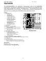
M68DEMO908GB60
Demonstration Board for Freescale MC9S08GB60
Includes DEMO9S08GB60-SP version
! Axiom Manufacturing • 2813 Industrial Lane • Garland, TX 75041
Email: [email protected] Web: http://www.axman.com !
M 6 8 D E M O 9 0 8 G B 6 0
0 1 / 1 2 / 0 5
CONTENTS
CAUTIONARY NOTES ...........................................................................................................................................................3
TERMINOLOGY ......................................................................................................................................................................3
FEATURES................................................................................................................................................................................4
GETTING STARTED...............................................................................................................................................................5
REFERENCE DOCUMENTATION .................................................................................................................................................5
M68DEMO908GB60 STARTUP............................................................................................................................................6
What Do the Demo Programs Do?......................................................................................................................................6
Applying the Demo Programs .............................................................................................................................................7
TABLE1: Demo Program Option Selections .......................................................................................................................8
Selecting the Demo Programs .............................................................................................................................................8
TABLE 2: Demo Program Selection....................................................................................................................................8
DEBUG MONITOR OPERATION .........................................................................................................................................9
MONITOR MEMORY MAP: .................................................................................................................................................9
M68DEMO908GB60 BOARD OPERATION.......................................................................................................................10
POWER SUPPLY .................................................................................................................................................................10
ON_OFF Switch ................................................................................................................................................................10
Batteries.............................................................................................................................................................................10
PWR - Power Jack .............................................................................................................................................................10
PWR_SEL Option ..............................................................................................................................................................11
Y1 CRYSTAL ..........................................................................................................................................................................11
R3 (XPG2) and R4 (XPG1) Options ..................................................................................................................................11
SCI1 AND SCI2 PORTS ...........................................................................................................................................................11
COM_EN ...........................................................................................................................................................................12
SCI1 and SCI2 Connection................................................................................................................................................12
LED 1-5 INDICATORS.............................................................................................................................................................12
VRH_SEL AND 1.8V REFERENCE .........................................................................................................................................13
VRH_SEL...........................................................................................................................................................................13
JP2 – VREFL .....................................................................................................................................................................13
SW1–SW4 PUSH SWITCHES...................................................................................................................................................13
JP1 – PWM / DAC ................................................................................................................................................................14
M68DEMO908GB60 I/O PORT CONNECTORS ...............................................................................................................14
ANALOG AND PTB I/O PORT CONNECTOR ..........................................................................................................................14
MCU I/O PORT CONNECTOR..................................................................................................................................................15
DEBUG PORT ......................................................................................................................................................................15
2
M 6 8 D E M O 9 0 8 G B 6 0
0 1 / 1 2 / 0 5
Cautionary Notes
1) Electrostatic Discharge (ESD) prevention measures should be applied whenever handling
this product. ESD damage is not a warranty repair item.
2) Axiom Manufacturing does not assume any liability arising out of the application or use of
any product or circuit described herein; neither does it convey any license under patent
rights or the rights of others.
3) EMC Information on the M68DEMO908GB60 board:
a) This product as shipped from the factory with associated power supplies and cables, has
been verified to meet with requirements of CE and the FCC as a CLASS A product.
b) This product is designed and intended for use as a development platform for hardware
or software in an educational or professional laboratory.
c) In a domestic environment this product may cause radio interference in which case the
user may be required to take adequate prevention measures.
d) Attaching additional wiring to this product or modifying the products operation from the
factory default as shipped may effect its performance and also cause interference with
other apparatus in the immediate vicinity. If such interference is detected, suitable
mitigating measures should be taken.
Terminology
This development board applies option selection jumpers. Terminology for application of the
option jumpers is as follows:
Jumper on, in, or installed = jumper is a plastic shunt that fits across 2 pins and the
shunt is installed so that the 2 pins are connected with the shunt.
Jumper off, out, or idle = jumper or shunt is installed so that only 1 pin holds the shunt,
no 2 pins are connected, or jumper is removed. It is recommended that the jumpers be
idled by installing on 1 pin so they will not be lost.
This development board applies hard wired option selection for JP2 (VREFL). This option
selection applies a circuit trace between the option pads to complete a default connection. This
type connection places an equivalent Jumper Installed type option. The circuit trace between
the option pads may be cut with a razor blade or similar type knife to isolate the default
connection provided. Applying the default connection again can be performed by installing the
option post pins and shunt jumper, or by applying a wire between the option pads.
3
M 6 8 D E M O 9 0 8 G B 6 0
0 1 / 1 2 / 0 5
FEATURES
The M68DEMO908GB60 is an evaluation or demonstration board for the M9S08GB60
microcontroller. Development of applications is quick and easy with the included DB9 serial
cable, sample software tools, examples, and debug monitor. The prototyping area provides
space to apply the MCU I/O to your needs. The DEBUG port is provided for development tool
application and is compatible with HCS08 BDM interface cables and software.
Features:
♦ M9S08GB60 CPU
* 60K Byte Flash
* 4K Bytes Ram
* 56 I/O lines (64 pins)
* 5 channel TPM 2 Timer
* 3 channel TPM 1 Timer
* 8 Channel 10 BIT A/D
* SPI and IIC Serial Ports
* 2 x SCI Serial Ports
* Key Board Wake-up Ports
* BDM DEBUG Port
* Clock generator w/ FLL
* up to 40Mhz operation
♦ 32Khz Crystal
♦ Regulated +3.3V power supply
♦ SCI1 Serial Port w/ RS232 DB9-S Connector
* SCI1 Serial Port
♦ SCI2 Serial Port w/ RS232 DB9-S Connector
* SCI1 Serial Port
♦ Power ON/OFF switch
♦ User Components Provided
* 5 LED Indicators (PTF0-3, PTD0)
* 4 Push Switches (PTA4-7)
* Digital to Analog (PTD2, PTB1)
* 1.8Volt reference
♦ MCU I/O Port connector provides all digital I/O
♦ Analog or PTB I/O Port connector provides analog inputs or PTB I/O
♦ Prototype Area
♦ 2 x AA Battery Holder
♦ Supplied with DB9 Serial Cable, Documentation (CD),
Manual, and Batteries or Wall plug type power supply.
Specifications:
Board Size 4” x 4.5”
Power Input: +6 to +12VDC, 9VDC typical
Current Consumption: 30ma @ 9VDC input
4
M68DEMO908GB60
M 6 8 D E M O 9 0 8 G B 6 0
0 1 / 1 2 / 0 5
GETTING STARTED
The M68DEMO908GB60 single board computer is a fully assembled, fully functional
development board for the Freescale MC9S08GB60 microcontroller. Provided with 2 AA
batteries or wall plug power supply, and serial cable. Support software for this development
board is provided for Windows 95/98/NT/2000/XP operating systems.
Development board users should also be familiar with the hardware and software operation of
the target HCS08 device, refer to the provided Freescale User Manual for the device and the
HCS08 Reference Manual for details. The demonstration board purpose is to promote the
features of the 9S08GB60 device or to assist the user in quickly developing an application with
a known working environment. Users should be familiar with memory mapping, memory types,
and embedded software design for the quickest successful application development.
Application development may be performed by applying the embedded serial interface monitor,
or by applying a compatible HCS08 BDM cable with supporting host software. The monitor
provides an effective and low cost debug method. Note that when a BDM cable is applied to
the DEBUG Port for debugging, the BDM pod should be powered from an external supply.
The serial debug monitor is provided in the development board HCS08 device internal flash
memory and applies some HCS08 resources for operation. See the AN2140 application note
from Freescale for complete details. User applications operated under monitor control may be
configured for dedicated operation by applying the User Reset Vector (0xFBFE/F) and
programming the application into the device flash. The monitor will remain in protected flash
memory for future use if needed.
Reference Documentation
Reference documents are provided on the support CD in Acrobat Reader format.
AN2140 – HCS08 Serial Monitor application note.
9S08GB_GT60UM.pdf – 9S08GB60 user manual
HCS08RM.pdf – HCS08 core user manual with instruction set
M68DEMO908GB60_SCH_B.pdf – M68DEMO908GB60 board schematics
5
M 6 8 D E M O 9 0 8 G B 6 0
0 1 / 1 2 / 0 5
M68DEMO908GB60 STARTUP
If the DEMO board is supplied with batteries pre-installed, the position of the PWR_SEL option
jumper must be set to the 1-2 position to enable battery power.
There are four examples programmed into the M68DEMO908GB60 board. The programs are:
1) Debug monitor
2) Low-power stop3 demo
3) Analog-to-digital converter (ATD)/timer demo
4) Software-paced loop
The Debug Monitor is the most important program loaded into the MCU residing on the Demo
board. In conjunction with a program running on a host personal computer (PC), the debug
monitor enables users to program FLASH and debug their programs.
The remainder of the demo programs offer examples of some simple uses of the Demo board.
The Low-power stop3 demo illustrates the low-power capability of the MC9S08GB60
microcontroller operating in stop3 mode.
The ATD/timer demo shows two timers set up as pulse-width modulators (PWM). One of the
PWM outputs drives an integrator (DAC). The other PWM output drives an LED. The ATD
reads the voltage output from the integrator and modulates the intensity of the LED.
The Software-paced loop demonstrates a framework that users can implement in their
system to periodically execute user routines.
What Do the Demo Programs Do?
The Stop3 demo program is the default program executed at power up if no pushbuttons are
held down. This program demonstrates operation of the microcontroller in low-power stop3
mode. The program uses the real time interrupt (RTI) to recover from stop3 mode.
In stop3 mode, clocks are halted and only IRQ, KBI, LVI and RTI interrupts can occur. For this
reason when using the serial debugger you can not trace through the demo code once you
have reached a stop instruction.
If you are using the serial debugger and you press the go button on the debugger, and test 1 is
entered (No buttons pressed) you will no longer be able to halt or trace the demo code. This is
because there are no clocks to the serial communications module.
If you observe LED1, located at the bottom left corner of the DEMO board, it will quickly flash
once approximately twice a second. The LED is on for about 600 microseconds. While the
LED is off, the MCU is in low-power stop3 mode and will remain in stop3, for approximately
one half second, until the next RTI.
6
M 6 8 D E M O 9 0 8 G B 6 0
0 1 / 1 2 / 0 5
The Software-paced loop demo program is executed when SW2 is held down at power-up.
The software-paced loop program blinks LED1 and LED4. LED1 will blink on and off every
second. LED4 will blink on and off every two seconds. Both LEDs blink at a 50% duty cycle.
The ATD/timer demo program is executed when SW3 is held down at powerup. Timer 1,
channel 2, is set up as a PWM output and is connected to a resistor-capacitor filter network,
composing a digital-to-analog converter (DAC). As the duty cycle on timer 1, channel 2,
changes, the voltage on the top of the capacitor in the DAC will change. The output from the
DAC is fed into the input to the ATD, channel 1. Timer 1, channel 0, is connected to LED5.
Timer 1, channel 0, is also set up as a PWM output. When the duty cycle of timer 1, channel 0,
is increased or decreased, the intensity of LED5 will follow the PWM duty cycle. The PWM
duty cycle of timer 1 channel 2 is increased by pushing SW1. The PWM duty cycle of timer 1,
channel 2, is decreased by pushing SW2. Thus, pushing SW1 or SW2 will change the intensity
of LED5.
The Debug Monitor program is executed when SW4 is held down at powerup. The serial
debugger, when applied with a host PC and associated debug interface program, enables a
user to erase device FLASH memory, program FLASH memory, load application programs,
and debug the application programs. The debug monitor dedicates SCI1 as its connection to
the host PC and does not use the traditional background debug mode, thus eliminating the
necessity for a background debug mode cable. Free software is available for execution on a
PC as an interface to the monitor. Refer to application note AN2140 for a full explanation for
using the debugger. The debugger is enabled when SW4 is held down at system power-up.
Applying the Demo Programs
Before you can run the demo programs, jumpers must be installed on the Demo board.
Depending on which programs you plan to run, jumpers will be installed in a different
configuration. Demo programs are selected at powerup from the state of three of the
pushbutton switches: SW2, SW3, and SW4, located on the bottom left-edge of the Demo
board.
PWR_SEL jumper block selects the source of power for the Demo board. If the Demo board is
to be powered by on-board batteries, install a jumper on the PWR_SEL block jumper, positions
1 to 2. If the PC board is to be powered by an external power supply connected to the PWR
connector, install a jumper on the PWR_SEL block jumper, positions 2 to 3.
If you want to test the stop3 mode for lowest power consumption, refer to Table 1 and install
the option jumpers on the Demo board per Column A. In this configuration, no power is applied
to the RS-232 level shifter. The remainder of the demo programs apply the option jumper
configuration of Column B.
If it is not important how much current the Demo board draws from the batteries during the
stop3 mode demo program, install the option jumpers per Column B of Table 1. Installing
jumpers as per Column B, extra current will be consumed by the RS-232 level shifter circuit.
To use the monitor program, connect a straight through DB-9 serial cable between the COM
port on the PC and the SCI1 connector on the Demo board.
7
M 6 8 D E M O 9 0 8 G B 6 0
0 1 / 1 2 / 0 5
TABLE1: Demo Program Option Selections
Jumper Name
PWR_SEL
COM_EN 1
COM_EN 2
COM_EN 3
COM_EN 4
COM_EN 5
VRH_SEL 1
VRH_SEL 2
VRH_SEL 3
VRH_SEL 4
VRH_SEL 5
JP1
LED_EN 1
LED_EN 2
LED_EN 3
LED_EN 4
LED_EN 5
(pins 1-2)
(pins 3-4)
(pins 5-6)
(pins 7-8)
(pins 9-10)
(pins 1-2)
(pins 3-4)
(pins 5-6)
(pins 7-8)
(pins 9-10)
(pins 1-2, 3-4)
(pins 1-2)
(pins 3-4)
(pins 5-6)
(pins 7-8)
(pins 9-10)
Column A
Stop3 Low-Power Mode Only
See text
Out
Out
Out
Out
Out
Out
Out
Out
Out
In
In
In
In
In
In
In
Column B
All Other Modes
See text
In
In
In
In
In
Out
Out
Out
Out
In
In
In
In
In
In
In
Selecting the Demo Programs
Three pushbutton switches are used by the Demo board’s software to select the demo
programs. The switches are SW2, SW3, and SW4. The switches are read at power-on reset
(POR). Hold down the pushbutton of choice while applying power. Apply power to the demo
PC board by sliding the ON_OFF switch, located on the top center of the Demo board, toward
the top of the board. After the ON_OFF switch is moved to the on position, you can release the
pushbutton SWx. The actions of the switches are shown in Table 2.
TABLE 2: Demo Program Selection
Switch (SWx)
No Switch held down
SW2
SW3
SW4
Demo Program
Stop3 demo
Software-paced loop demo
ATD/timer demo
Debug monitor
NOTES:
1) When power is applied to the Demo board, if no switches are held down, the
low-power stop3 demo program will execute as the default.
2) When power is applied to the Demo board and SW2 is held down, the software-paced loop
demo program will execute.
3) When power is applied to the Demo board and SW3 is held down, the ATD/timer demo
program will execute.
4) When power is applied to the Demo board and SW4 is held down, the serial Debug
Monitor program will execute. A host serial debug program must be executed on your PC
to use the monitor program. To use the monitor program, connect a straight through DB-9
serial cable between COM port on the personal computer and SCI1 on the Demo board.
8
M 6 8 D E M O 9 0 8 G B 6 0
0 1 / 1 2 / 0 5
DEBUG MONITOR OPERATION
See the AN2140 application note on the monitor for complete details of operation. Basic
operation is provided in this manual. The monitor occupies 1K bytes of flash memory and
about to 50 bytes of stack space. It provides a binary command set via the SCI1 port.
COMMUNICATION:
The monitor provides 115.2K baud serial communication on the SCI1 interface port.
POWER ON or RESET PROMPT:
The monitor will provide a binary prompt to the Demo board serial SCI1 port.
COMMANDS:
No user commands can be applied with a keyboard with software such as HyperTerminal or
AxIDE. The monitor commands are binary and not compatible with keyboard (ASCII) entry or
display. Host based software should interface with the monitor on the serial communication
port to provide development support.
INTERRUPT SERVICE SUPPORT:
The monitor enables automatic hardware vector relocation in the 9S08GB60 so user interrupt
vectors appear from 0xFBCC to 0xFBFF. User will not have access to the SCI1, SWI, and
RESET vectors while the monitor is operating. Programming the user Reset vector will cause
the monitor to execute the user program on Reset. See the AN2140 application note for user
interrupt application.
MONITOR MEMORY MAP:
0x0000 0x007F
0x0080 0x107F
0x1080 0x17FF
0x1800 0x182B
0x182C 0xFBCB
0xFBCC 0xFBFF
0xFC00 0xFFFF
9S08GB60 Direct Page Register Space.
See the 9S08GB60 User Manual for details
9S08GB60 ram memory space
Initial Monitor Stack Pointer = 0x107F
Lower flash block – User application memory
9S08GB60 High Page Register block
User Application Flash Memory
User Interrupt Vectors
See AN2140 for details on application
Monitor Flash Memory Space (Protected)
9
M 6 8 D E M O 9 0 8 G B 6 0
0 1 / 1 2 / 0 5
M68DEMO908GB60 Board Operation
The M68DEMO908GB60 board provides input and output features to assist in application
development. These features may be isolated from the applied HCS08 I/O ports by the option
jumpers. This allows alternate use of the HCS08 I/O ports for other application and connection
on the I/O port connectors. Caution should be observed so that the HCS08 I/O port pin
applied to an on board feature is not also applied to external components by the user.
POWER SUPPLY
Input power is applied by external connection to the J1 power jack and 3.3V regulator or
directly from the on board batteries. The input supply is selected by the PWR_SEL option.
ON_OFF switch operation will enable either the regulated 3.3V or battery supply selected by
the PWR_SEL option.
ON_OFF Switch
The ON_OFF slide switch provides board power on and off control. With the switch in the ON
position, either the regulated +3.3V or battery supply is enabled to the Demo board circuits.
Batteries
The Demo board provides for two AA type batteries to be installed. Note the polarity
indications in the battery holder when installing batteries. The batteries will provide a nominal
3V supply when applied. See the PWR_SEL option for selecting battery operation.
PWR - Power Jack
PWR provides external power input to the board. The PWR jack accepts a standard 2.0 ~
2.1mm center barrel plug connector (positive voltage center) to provide the +VIN supply of +5
to +12 VDC (+9VDC typical).
+Volts, 2mm center
10
M 6 8 D E M O 9 0 8 G B 6 0
0 1 / 1 2 / 0 5
PWR_SEL Option
The PWR_SEL option selects the input supply to the Demo board circuits. Either the on board
battery pack or external supply with 3.3V regulator may be selected.
Battery In
1
2
3
J1 / 3.3V In
1
2
3
Y1 Crystal
Crystal Y1 provides a 32.768Khz base operating frequency to the HCS08 device. The user
should refer to the HCS08 device user manual for information on frequency selection. User
should also note that the HCS08 PTG1 and PTG2 I/O pins provide the oscillator connection
and these I/O pins are not provided to the MCU_PORT by default. See the R3 and R4 option
for changing this configuration.
R3 (XPG2) and R4 (XPG1) Options
R3 and R4 component locations are open by default to isolate the sensitive crystal oscillator
connections from the MCU_PORT XPG2 and XPG1 locations. The user may connect the
PTG1/PTG2 to the XPG1/XPG2 locations by installing a 0805 size 0 ohm resistor or wire
jumper across the R4/ R3 component locations respectfully.
SCI1 and SCI2 Ports
The COM_EN option jumper block provides HCS08 SCI I/O ports to the SCI1 and SCI2
communication port connections on the Demo board. This allows the user to apply the
provided communication transceiver, or to apply the associated I/O to other purposes. The
option jumper positions should be reviewed first if any operational problems are encountered
with the SCI1 or SCI2 ports.
11
M 6 8 D E M O 9 0 8 G B 6 0
0 1 / 1 2 / 0 5
COM_EN
COM_EN
Position
1
(pins 1-2)
HCS08 Port
2
3
4
5
PTE0/TxD1
PTE1/RxD1
PTC0/TxD2
PTC1/RxD2
(pins 3-4)
(pins 5-6)
(pins 7-8)
(pins 9-10)
COM Signal
I/O PORT
Connector
RS232 Transceiver Enable
(U3)
SCI1 TxD OUT
SCI1 RxD IN
SCI2 TxD OUT
SCI2 RxD IN
37
38
17
18
Notes:
1) COM_EN position 1 will power off the RS232 transceiver (U3) when open.
SCI1 and SCI2 Connection
The SCI1 and SCI2 ports provide standard 9 pin connection with RS232 type interface to the
HCS08 SCI1 and SCI2 peripherals. Refer to the COM_EN options for enabling the HCS08
signals applied to these ports. The SCI1 port is applied by default with the Debug Monitor. The
HCS08 TxD1/2 and RxD1/2 signals are converted to RS232 levels by U3 and provided to the
DB9 serial connectors. Following is the DB9S connection reference.
SCI1 and SCI2
1 1
X
TXD1 2 6 6
RXD1 3 7 7
4 4 8 8
GND 5 9 9
Female DB9 connector that interfaces to the HCS08 internal
SCI1 serial port via the U3 RS232 transceiver. It applies simple
2 wire asynchronous serial without flow controls.
1,4,6 connected and 7,8 connected
LED 1-5 Indicators
LED Indicators 1–5 are enabled to HCS08 I/O ports by the LED_EN option bank. The LED
indicators will light with a logic low signal applied from the respective HCS08 I/O port if the
option is installed. The Demo board user should be familiar with the input and output
application so that port conflicts do not occur. Following is the LED connection reference
table:
1
2
3
4
5
LED_ EN
Position
(pins 1-2)
(pins 3-4)
(pins 5-6)
(pins 7-8)
(pins 9-10)
LED INDICATOR
LED 1
LED 2
LED 3
LED 4
LED 5
HCS08 PORT
PTF0
PTF1
PTF2
PTF3
PTD0/TPM1CH0
Note: LED indicators are active logic low.
12
I/O PORT
CONNECTOR
47
48
45
46
27
M 6 8 D E M O 9 0 8 G B 6 0
0 1 / 1 2 / 0 5
VRH_SEL and 1.8V Reference
A 1.8 Volt reference circuit (U2) is provided for demonstration program application and user
application if wanted. The VRH_SEL option bank selects the input and output configuration of
the 1.8V reference circuit. Caution should be applied when selecting the VRH_SEL options so
that supply or port conflicts do not occur.
VRH_SEL
1
2
3
4
5
VRH_SEL
POSITION
(pins 1-2)
(pins 3-4)
(pins 5-6)
(pins 7-8)
(pins 9-10)
INPUT SIGNAL
OUTPUT SIGNAL
VDDAD (3.3V)
HCS08 PTF7
1.8V reference (U2 out)
1.8V reference (U2 out)
VDDAD
U2 Input Supply
U2 Input Supply
PTB0 / ATD0
VREFH
VREFH
I/O PORT
Connection
MCU I/O pin 42
Analog I/O pin 1
Analog I/O pin 9
Analog I/O pin 9
OPERATION
U2 is powered on
PTF7 = 1 for U2 powered On.
1.8V ref to ATD0 channel
VREFH = 1.8V Reference
VREFH = VDDAD (3.3V)
Notes:
1) VRH_SEL jumper positions 1 (pins 1-2) and 2 (pins 3-4) must not be installed at the same
time.
2) VRH_SEL jumper positions 4 (pins 7-8) and 5 (pins 9-10) must not be installed at the same
time.
JP2 – VREFL
JP2 is default closed by circuit trace jumper that provides a VREFL connection to Ground
potential. The user should not need to modify this connection.
SW1–SW4 Push Switches
The push switches provide momentary active low input for user applications. The switches
provide input to HCS08 ports PTA4 – PTA7. Input ports PTA4 – PTA7 provide KBD4 – KBD7
input interrupt capability also. The switches also provide the Demo program selection during
Reset or power on condition if the demo program is installed in the flash memory. (Refer to
M68DEMO908GB60 STARTUP).
SW4 on HCS08 PTA7 also provides the force debug monitor active operation. Holding SW4
down during power up will force the debug monitor active if it is still resident in the flash
memory.
13
M 6 8 D E M O 9 0 8 G B 6 0
0 1 / 1 2 / 0 5
JP1 – PWM / DAC
JP1 options enable a PWM signal filter on HCS08 port PTD2/TPM1CH2 to provide a digital to
analog conversion into HCS08 PTB1/ATD1 analog input. This circuit is for demonstration of
analog signal generation with a PWM timer output. The PTB1/ATD1 connection provides for
measuring the analog signal value generated in the circuit.
JP1 Jumper Installation
1
2
3
4
Notes:
1) JP1 position 1-2 connects PTD2/TPM1CH2 to the R-C filter input.
2) JP1 position 3-4 connects PTB1/ATD1 to the R-C filter output.
M68DEMO908GB60 I/O PORT CONNECTORS
ANALOG and PTB I/O Port Connector
This port connector provides access to the Port B I/O or Analog input signals.
PTB0/AD0
PTB2/AD2
PTB4/AD4
PTB6/AD6
VREFH
1
3
5
7
9
2
4
6
8
10
PTB1/AD1
PTB3/AD3
PTB5/AD5
PTB7/AD7
VREFL
Notes:
1) PTB0 provides 1.8V reference input if enabled. (VRH_SEL)
2) PTB1 provides DAC filter input if enabled. (JP1)
3) VREFH is optioned by VRH_SEL.
14
M 6 8 D E M O 9 0 8 G B 6 0
0 1 / 1 2 / 0 5
MCU I/O Port Connector
This port connector provides access to all the 9S08GB60 I/O ports except PTB.
PTA6/KBD6
PTA4/KBD4
PTA2/KBD2
PTA0/KBD0
VDD
PTC6
PTC4/CLKOUT
PTC2/SDA
PTC0/TXD2
VDD
PTD6/TPM2CH3
PTD4/TPM2CH1
PTD2/TPM1CH2
PTD0/TPM1CH0
VDD
PTE6
PTE4/MOSI
PTE2/SS*
PTE0/TXD1
VDD
PTF6
PTF4
PTF2
PTF0
VDD
PTG6
PTG4
PTG2/EXTAL
PTG0/BGND/MS
RESET*
1
3
5
7
9
11
13
15
17
19
21
23
25
27
29
31
33
35
37
39
41
43
45
47
49
51
53
55
57
59
2
4
6
8
10
12
14
16
18
20
22
24
26
28
30
32
34
36
38
40
42
44
46
48
50
52
54
56
58
60
PTA7/KBD7
PTA5/KBD5
PTA3/KBD3
PTA1/KBD1
GND
PTC7
PTC5
PTC3/SCL
PTC1/RXD2
GND
PTD7/TPM2CH4
PTD5/TPM2CH2
PTD3/TPM2CH0
PTD1/TPM1CH1
GND
PTE7
PTE5/SPSCK
PTE3/MISO
PTE1/RXD1
GND
PTF7
PTF5
PTF3
PTF1
GND
PTG7
PTG5
PTG3
PTG1/XTAL
IRQ
Notes:
1) PTA4-7 also provide
Push Switch SW1-4
2) PTE0 –1 provide SCI1
I/O to SCI1 Port if
enabled.
3) PTC0-1 provide SCI2
I/O to SCI2 port if
enabled.
4) PTD0 provides LED5
output if enabled.
5) PTG1-2 are the Y1
XTAL and EXTAL
signals by default. R3
and R4 isolate the
MCU PORT XPG1 and
XPG2 pins to prevent
crystal operation
interference.
6) PTG0 is the BGND
signal if a BDM is
connected.
7) PTF0-F3 provide LED1
– 4 output if enabled.
DEBUG PORT
The Debug or BDM port is a 6 pin header compatible with a Freescale Background Debug
Mode (BDM) Pod. This allows the connection of a background debugger for software
development, programming and debugging in real-time without using HCS08 I/O resources.
BGND/PTG0 1 2 GND
3 4 /RESET
5 6 +3.3V
See the HCS08 Reference Manual for complete
documentation of the BDM.
15