1
6
6.1
Overview
The board
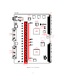
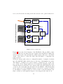
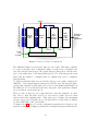
The i - SADC108032 module is made according to the 6U VME mechanical
standard. A schematic is shown in figure 1.
Two 34 pin flat cable connectors bring the analogue differential signals to
the 32 Analog Devices AD9214-80 analogue-to-digital converters.
The digital samples are read by two Xilinx XC2V1000 FPGAs named ’ZR0’ and
’ZR1’. The ZR chips perform the digital data processing (latency compensation, buffering, zero suppression, data formatting) and each of them is
connected to 16 channels: ZR0 to input channels 0 to 15, ZR1 to input
channels 16 to 31.
The data go from the ZR chips over 16 bit wide links to the so called ’HL’ chip.
This Xilinx XCV100E FPGA multiplexes the data from the ZR FPGAs and
writes them out to the HOTLink Transmitter which serialises and encodes the
data so that they can be sent over the optical transceiver to the destination
module. The HL chip also provides the interface to load and configure the
two ZR FPGAs.
The IEEE-1014 back plane of the VME crate is only used to provide +5 V
and −12 V power.
7