1
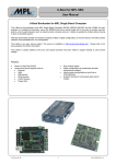
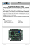
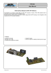
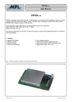
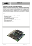
IDE2PCC User Manual High-Tech • Made in Switzerland IDE2PCC The IDE2PCC is a cost effective and easy to use adapter for connecting PCMCIA PC Cards ATA with true IDE interface (PC Cards) to the standard IDE port of a single board computer (SBC) from MPL or other manufacturers. For mechanical fixing in MPL’s PIP family, the IDE2PCC can be connected to the PC/104 slot. The PC Card slot is then available on the right side of the PIP case. For mounting on top of other SBCs, the mounting holes defined in the PC/104 specification are available. The IDE signals are connected to the IDE2PCC via a standard 40 or 44 pin IDE cable. The power is distributed either with the 44 pin IDE cable or through the PC/104 connector. There are two standard variants of the IDE2PCC available. Others are possible on request: IDE2PCC-1A44: With PC Card interface, 44 pin IDE connector and PC/104 connector. (For PIPx / MIPx with the possibility to install an additional PC/104 card on top of it, no 12 V PC Card support). IDE2PCC-1N44: With PC Card interface, 44 pin IDE connector without PC/104 connector (For general use with any kind of SBC with IDE port, no 12 V PC Card support). At the time of writing of this manual the following MPL products are supported: • PIP405 • PIP5, PIP6, PIP7, PIP8 • MIP405 • MIP520 Features: • • • • • • • 2003 by MPL AG Easy to use & inexpensive PC/104 form factor Optional separate power connector 44 pin (optional 40 pin) IDE connector Master / Slave selection possible Optional 2 PC Card Slots (Master & Slave) For bigger order quantities several assembly options are available. Please feel free to contact MPL AG for further information. 1 IDE2PCC User Manual High-Tech • Made in Switzerland TABLE OF CONTENTS 1. 1.1 1.2 1.3 1.4 2. INTRODUCTION.........................................................................................................................................................3 ABOUT THIS MANUAL .........................................................................................................................................3 SAFETY PRECAUTIONS AND HANDLING..........................................................................................................3 ELECTROSTATIC DISCHARGE (ESD) PROTECTION........................................................................................3 EQUIPMENT SAFETY ..........................................................................................................................................3 GENERAL INFORMATION .........................................................................................................................................4 2.1 DESCRIPTION ......................................................................................................................................................4 2.2 SPECIFICATIONS.................................................................................................................................................4 2.2.1 SUPPORTED CARD TYPES.......................................................................................................................4 2.2.2 POWER SUPPLY ........................................................................................................................................4 2.2.3 OPERATING ENVIRONMENT ....................................................................................................................4 2.2.4 STORAGE ENVIRONMENT........................................................................................................................4 3. ASSEMBLY OF THE IDE2PCC ..................................................................................................................................4 4. PIN ASSIGNEMENT AND SIGNAL DESCRIPTION ...................................................................................................5 4.1 4.2 4.3 4.4 5. 5.1 5.2 5.3 5.4 5.5 44 PIN IDE CONNECTOR (J1) .............................................................................................................................5 40 PIN IDE CONNECTOR (J2) .............................................................................................................................5 PC/104 CONNECTOR (J5 / J6).............................................................................................................................6 OPTIONAL 4 PIN POWER CONNECTOR (J7).....................................................................................................6 USE OF THE IDE2PCC ..............................................................................................................................................7 SELECTION OF THE NEEDED IDE2PCC............................................................................................................7 SLIDE SWITCH CONFIGURATION ......................................................................................................................7 INSTALLING THE IDE2PCC .................................................................................................................................7 USE OF THE PC CARDS......................................................................................................................................7 BOOT FROM IDE2PCC ........................................................................................................................................8 6. MECHANICAL DATA ..................................................................................................................................................9 7. COPYRIGHT, REVISION HISTORY.........................................................................................................................12 8. DISCLAIMER ............................................................................................................................................................12 9. SUPPORT.................................................................................................................................................................12 2003 by MPL AG 2 MEH-10093-001 Rev. A IDE2PCC User Manual High-Tech • Made in Switzerland 1. INTRODUCTION 1.1 ABOUT THIS MANUAL This manual provides all the information necessary to handle and configure the IDE2PCC. The manual is written for technical personnel responsible for integrating and using the IDE2PCC into their systems. 1.2 SAFETY PRECAUTIONS AND HANDLING For personal safety and safe operation of the IDE2PCC, follow all safety procedures described here and in other sections of the manual. • Remove power from the system before installing (or removing) the IDE2PCC to prevent the possibility of personal injury (electrical shock) and / or damage to the product. • Handle the product carefully; i.e. dropping or mishandling the IDE2PCC can cause damage to assemblies and components. • Do not expose the equipment to moisture. NOTE: There are no user-serviceable components on the IDE2PCC. 1.3 ELECTROSTATIC DISCHARGE (ESD) PROTECTION Though there are no components on the IDE2PCC that are sensible to electrostatic discharge some precautions were taken to protect the circuits of the IDE interface connected to the IDE2PCC. The electrostatic charge of the PC Card to be inserted is shunt to the system ground during insertion via the card rails. The connector pins itself do not have additional protection! 1.4 EQUIPMENT SAFETY Great care is taken by MPL that all its products are thoroughly and rigorously tested before leaving the factory to ensure that they are fully operational and conform to specification. However, no matter how reliable a product, there is always the remote possibility that a defect may occur. The occurrence of a defect on this device may, under certain conditions, cause a defect to occur in adjoining and/or connected equipment. It is your responsibility to protect such equipment when installing this device. MPL accepts no responsibility whatsoever for such defects, however caused. 2003 by MPL AG 3 MEH-10093-001 Rev. A IDE2PCC User Manual High-Tech • Made in Switzerland 2. GENERAL INFORMATION 2.1 DESCRIPTION The IDE2PCC is a cost effective and easy to use adapter for connecting PCMCIA PC Cards ATA (PC Cards) to the standard IDE port of a single board computer (SBC) from MPL or other manufacturers. With IDE2PCC the storage cards are used like IDE hard disks. They are not hot plug capable in IDE2PCC. If you require hot plug use the PCCARD of MPL AG. 2.2 SPECIFICATIONS 2.2.1 SUPPORTED CARD TYPES Only PCMCIA PC Cards ATA with true IDE interface (PC Cards) are supported. These cards are memory cards and have a true IDE mode and so they can be directly connected to the standard IDE/ATA interface via IDE2PCC. For I/O cards like MODEM, LAN, .. please use MPL’s PCCARD (www.mpl.ch). 2.2.2 POWER SUPPLY • • IDE2PCC accepts only 5 V PC Cards. Care has to be taken with defective storage cards. There are no protection circuits on the IDE2PCC against increasing current flow. All the current provided by the SBC can flow to the storage card. 2.2.3 OPERATING ENVIRONMENT • • Temperature range: -20° C to +65° C Relative humidity: 95% maximum (non condensing) 2.2.4 STORAGE ENVIRONMENT • • Temperature range: -20°C to +65°C Relative humidity: 95% maximum (non condensing) 3. ASSEMBLY OF THE IDE2PCC Figure 1: IDE2PCC With PCMCIA Slot J4 J5 / J6 J1 J2 J7 S1 PCMCIA PC Card ATA Slot PC/104 connectors (stack trough, optional) 44 pin IDE connector optional 40 pin IDE connector (instead of the 44 pin IDE connector) optional separate 4 pin power connector (with 40 pin IDE connector) Slide switch for Master / Slave selection 2003 by MPL AG 4 MEH-10093-001 Rev. A IDE2PCC User Manual High-Tech • Made in Switzerland 4. PIN ASSIGNEMENT AND SIGNAL DESCRIPTION 4.1 44 PIN IDE CONNECTOR (J1) Pin 1 3 5 7 9 11 13 15 17 19 21 23 25 27 29 31 33 35 37 39 41 43 Signal /RESET D7 D6 D5 D4 D3 D2 D1 D0 GND DRQ IOW IOR IORDY DACK IRQ A1 A0 CS0 /DASP VCC5 GND Description Reset Data bit 7 Data bit 6 Data bit 5 Data bit 4 Data bit 3 Data bit 2 Data bit 1 Data bit 0 Ground DMA request I/O write strobe I/O read strobe I/O ready DMA acknowledge Interrupt request Address 1 Address 0 Chip select 0 Device active, device 1 present +5 V Ground Pin 1 Pin 2 Pin 43 Pin 44 Description Ground Data bit 8 Data bit 9 Data bit 10 Data bit 11 Data bit 12 Data bit 13 Data bit 14 Data bit 15 Key / not connected Ground Ground Ground Not connected on IDE2PCC Ground I/O chipselect16 Passed diagnostic Address 2 Chip select 1 Ground +5 V Ground Signal GND D8 D9 D10 D11 D12 D13 D14 D15 KEY GND GND GND NC (CSEL) GND IOCS16 /PDIAG A2 CS1 GND VCC5 GND Pin 2 4 6 8 10 12 14 16 18 20 22 24 26 28 30 32 34 36 38 40 42 44 Signal GND D8 D9 D10 D11 D12 D13 D14 D15 KEY GND GND GND NC (CSEL) GND IOCS16 /PDIAG A2 CS1 GND Pin 2 4 6 8 10 12 14 16 18 20 22 24 26 28 30 32 34 36 38 40 Table 1: Pin Numbering On The 44 Pin IDE Connector J1 4.2 40 PIN IDE CONNECTOR (J2) Pin 1 3 5 7 9 11 13 15 17 19 21 23 25 27 29 31 33 35 37 39 Signal /RESET D7 D6 D5 D4 D3 D2 D1 D0 GND DRQ IOW IOR IORDY DACK IRQ A1 A0 CS0 /DASP Description Reset Data bit 7 Data bit 6 Data bit 5 Data bit 4 Data bit 3 Data bit 2 Data bit 1 Data bit 0 Ground DMA request I/O write strobe I/O read strobe I/O ready DMA acknowledge Interrupt request Address 1 Address 0 Chip select 0 Device active, device 1 present Pin 1 Pin 2 Pin 39 Pin 40 Description Ground Data bit 8 Data bit 9 Data bit 10 Data bit 11 Data bit 12 Data bit 13 Data bit 14 Data bit 15 Key / not connected Ground Ground Ground Not connected on IDE2PCC Ground I/O chip select 16 Passed diagnostic Address 2 Chip select 1 Ground Table 2: Pin Numbering On The 40 Pin IDE Connector J2 2003 by MPL AG 5 MEH-10093-001 Rev. A IDE2PCC User Manual High-Tech • Made in Switzerland 4.3 PC/104 CONNECTOR (J5 / J6) The PC/104 Connector connects the PC/104 signals from add on cards through the IDE2PCC to the PIPx / MIPx. Only the power supply lines are required by the IDE2PCC in certain assembly variants. Number 0 1 2 3 4 5 6 7 8 9 10 11 12 13 14 15 16 17 18 19 20 21 22 23 24 25 26 27 28 29 30 31 32 Row A -/IOCHCK SD7 SD6 SD5 SD4 SD3 SD2 SD1 SD0 IOCHRDY AEN SA19 SA18 SA17 SA16 SA15 SA14 SA13 SA12 SA11 SA10 SA9 SA8 SA7 SA6 SA5 SA4 SA3 SA2 SA1 SA0 GND Row B -GND RSTDRV +5 V IRQ9 (-5 V)*1 DRQ2 -12 V /ENDXFR +12 V GND (Key) /SMEMW /SMEMR /IOW /IOR /DACK3 DRQ3 /DACK1 DRQ1 /REFRESH SYSCLK IRQ7 IRQ6 IRQ5 IRQ4 IRQ3 /DACK2 TC BALE +5 V OSC GND GND Row C GND /SBHE LA23 LA22 LA21 LA20 LA19 LA18 LA17 /MEMR /MEMW SD8 SD9 SD10 SD11 SD12 SD13 SD14 SD15 NC -------------- Row D GND /MEMCS16 /IOCS16 IRQ10 IRQ11 IRQ12 IRQ15 IRQ14 /DACK0 DRQ0 /DACK5 DRQ5 /DACK6 DRQ6 /DACK7 DRQ7 +5 V /MASTER GND GND -------------- Pinout AB 0 1 DC 19 32 Table 3: PC/104 Connector NOTE: Only the shaded fields are connected to the IDE2PCC PCB 4.4 OPTIONAL 4 PIN POWER CONNECTOR (J7) The power connector corresponds to a standard 3.5 inch floppy drive power connector. A sample part number of the used connector is 171 826-4 from Tyco AMP. A mating counterpart is the 171822-4 from Tyco AMP. Number Signal Description Pinout 1 VCC12 +12 V 2 GND Ground 3 GND Ground 4 VCC5 +5 V Pin 1 Table 4: Optional Power Connector 2003 by MPL AG 6 MEH-10093-001 Rev. A IDE2PCC User Manual High-Tech • Made in Switzerland 5. USE OF THE IDE2PCC 5.1 SELECTION OF THE NEEDED IDE2PCC The signals for connecting a PC Card to the IDE bus are distributed to the IDE2PCC via a 40-pin or a 44-pin IDE cable. Dependent on the available IDE port on the SBC system you must select a IDE2PCC with 40-pin or one with 44-pin IDE connector. The power is distributed to the IDE2PCC either via the PC/104 connector, the 44 pin IDE connector or the separate power connector. On MPL’s PIP family the IDE2PCC is mounted on the PC/104 connector and fixed through the PC/104 mounting holes. A IDE2PCC with PC/104 connector is needed for stacking through the PC/104 signals from PIPx to other PC/104 cards. 5.2 SLIDE SWITCH CONFIGURATION The slide switch on IDE2PCC is for master / slave configuration of the PC Card slots on the IDE bus. LS, CF: Master HS: Master Figure 2: Slide Switch for Master/Slave Selection Switch setting LS, CF: Master HS: Master Effect Lower PC Card Slot (if double slot is used): Higher PC Card Slot (if double slot is used): Single PC Card Slot: Lower PC Card Slot (if double slot is used): Higher PC Card Slot (if double slot is used): Single PC Card Slot: Master Slave Master Slave Master Slave Table 5: Slide Switch Settings Change the Master / Slave configuration only while the power is off. PC Cards detect this setting only during power up. 5.3 INSTALLING THE IDE2PCC Depending on the assembly variant of your IDE2PCC the following procedure may vary slightly. However the principal installing steps remain the same. Plug the IDE cable to your systems IDE connector. Plug the IDE2PCC onto the PC/104 connector of your system or fasten it mechanically into your chassis if you don't use the PC/104 for mounting. Plug the other end of the IDE cable to J1 / J2 of the IDE2PCC. Caution: Be sure that pin 1 of J1 / J2 of the IDE2PCC meets pin 1 of the host systems IDE port and that the cable connectors fit properly to the board connectors. If not powered by the PC/104 bus plug your power supply to J7 of the IDE2PCC. Select your desired operating mode with S1 (refer to 5.2) Insert your PC Card. 5.4 USE OF THE PC CARDS With IDE2PCC the storage cards are used like IDE hard disks. They are not hot plug capable in IDE2PCC. If you require hot plug use the PCCARD of MPL AG. 2003 by MPL AG 7 MEH-10093-001 Rev. A IDE2PCC User Manual High-Tech • Made in Switzerland 5.5 BOOT FROM IDE2PCC The IDE interface basically supports two different addressing modes: CHS (Cylinder, Head and Sector number) according to the hard disk architecture (the hard disks which are normally installed to the IDE port are internally organized in Cylinders Heads and Sectors) and LBA (Logical Block Addressing) which addresses the hard disk memory in a linear way. IDE devices (PC Cards in the IDE2PCC are working in true IDE mode) are in general not for use in different computer systems. Because the several BIOS’ have an other translation of the CHS numbers. There is no guarantee that a PC Card formatted and installed in a laptop or an other PC-System also can be used in e.g. a PIP6 (or also a third computer system). That is a systematic PC architecture problem. The best way for avoiding troubles with booting: Low level format (erase the Boot Sector) the needed PC Card, format it and make the installation of the operating system in the computer system that is intended to boot from this PC Card (just the way you do it with a new fix installed hard-drive). The other possibility is if you don’t want to install the PC Card on the end system, you must insure that the computer system you take for installing the PC Card and the computer system you take to use the PC Card have a BIOS that use the same IDE addressing (you reach the best results by using LBA mode). 2003 by MPL AG 8 MEH-10093-001 Rev. A IDE2PCC User Manual High-Tech • Made in Switzerland 90,15mm. 6. MECHANICAL DATA 95,89mm. Figure 3: Mechanical Dimensions Length: With: Holes: 2003 by MPL AG 90.2 mm 95.9 mm / 97.3 mm Pad 6.4mm / hole 3.2mm 9 MEH-10093-001 Rev. A IDE2PCC User Manual High-Tech • Made in Switzerland This page is intentionally left blank. 2003 by MPL AG 10 MEH-10093-001 Rev. A IDE2PCC User Manual High-Tech • Made in Switzerland This page is intentionally left blank. 2003 by MPL AG 11 MEH-10093-001 Rev. A IDE2PCC User Manual High-Tech • Made in Switzerland 7. COPYRIGHT, REVISION HISTORY Copyright © 2002 by MPL AG Elektronikunternehmen. All rights are reserved. Reproduction of this document in part or whole, by any means, is prohibited, without written permission from MPL AG Elektronikunternehmen. This Manual reflects the revision A of the IDE2PCC. Publication Date: November 2002 Manual Date Revision A Preliminary 27.09.2002 A 25.04.2003 Description Initial Write Add sections 5.3 and 5.5, correct some typos, add the picture, split the Manual for IDE2PCC and IDE2CF, add the front pages picture. 8. DISCLAIMER MPL AG has fully tested the IDE2PCC module and reviewed the documentation. However, MPL AG makes no warranty or representation, either expressed, or implied, with respect to this product, its quality, performance, merchantability, or fitness for a particular purpose. In no event will MPL AG be liable for direct, indirect, special, incidental, or consequential damages resulting from any defect in the product or its documentation, even if advised of the possibility of such damages. In particular MPL AG shall have no liability for any parts connected to this product. MPL AG reserves the right to make changes to any product herein to improve reliability, function or design. 9. SUPPORT In case of questions please feel free to contact us at our homepage (www.mpl.ch) or per email ([email protected]). Our Local Distributor: 2003 by MPL AG 12 MEH-10093-001 Rev. A