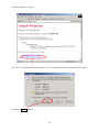
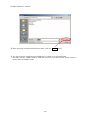
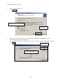
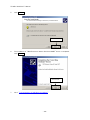
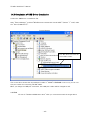
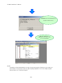
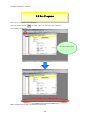
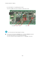
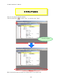
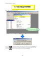
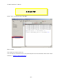
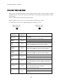
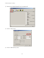
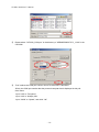
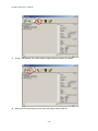
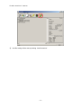
1
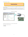
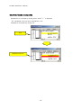
User’s Manual
TK-850/JG3H
Date published: Oct 2008
Rev. 1.0
© TESSERA TECHNOLOGY INC. 2008
Printed in Japan
TK-850/JG3H User’s Manual
Windows and Windows XP are registered trademarks or trademarks of Microsoft Corporation in the United States and/or
other countries.
・The information is subject to change without notice.
・No part of this document may be copied or reproduced in any form or by any means without prior written consent
of TESSERA TECHNOLOGY INC.. TESSERA TECHNOLOGY INC. assumes no responsibility for any errors that
may appear in this document.
・TESSERA TECHNOLOGY INC. does not assume any liability for infringement of patents, copyrights or other
intellectual property rights of third parties by or arising from the use of TESSERA TECHNOLOGY INC. products
listed in this document or any other liability arising from the use of such products. No license, express, implied or
otherwise, is granted under any patents, copyrights or other intellectual property rights of TESSERA
TECHNOLOGY INC. or others.
・Descriptions of circuits, software and other related information in this document are provided for illustrative
purposes in semiconductor product operation and application examples. The incorporation of these circuits,
software and information in the design of a customer's equipment shall be done under the full responsibility of the
customer. TESSERA TECHNOLOGY INC. assumes no responsibility for any losses incurred by customers or third
parties arising from the use of these circuits, software and information.
CAUTION
・Do not give any physical damage to this equipment such as dropping
・Do not superimpose voltage to this equipment.
・Do not use this equipment with the temperature below 0℃ or over 40℃.
・Make sure the USB cables are properly connected.
・Do not bend or stretch the USB cables.
・Keep this equipment away from water.
・Take extra care to electric shock.
・This equipment should be handled like a CMOS semiconductor device. The user must take all precautions to
avoid build-up of static electricity while working with this equipment.
・All test and measurement tool including the workbench must be grounded.
・The user/operator must be grounded using the wrist strap.
・The connectors and/or device pins should not be touched with bare hands.
-2-
TK-850/JG3H User’s Manual
Contents
CHAPTER 1 PREPARATION.....................................................................................................................................................7
1.1 Development Tools / Software..............................................................................................................................8
1.2 Installation of Development Tools ........................................................................................................................9
1.2.1 Installation Package .....................................................................................................................................9
1.2.2 Installation of Development Tools..........................................................................................................9
1.3 Sample Programs...................................................................................................................................................... 14
1.3.1 Preparation of Sample Programs......................................................................................................... 14
1.3.2 Overview of Sample Programs ............................................................................................................. 17
1.4 Installation of USB Driver ..................................................................................................................................... 18
1.4.1 Installation on Windows XP.................................................................................................................... 19
1.4.2 Installation on Windows 2000 ................................................................................................................ 22
1.4.3 Completion of USB Driver Installation............................................................................................... 25
CHAPTER 2 EXPERIENCES................................................................................................................................................... 26
2.1 Start PM+ .................................................................................................................................................................... 28
2.2 What is PM+................................................................................................................................................................ 29
2.3 Load Workspace (project) ..................................................................................................................................... 31
2.4 Set Options................................................................................................................................................................. 33
2.4.1 "Extend" Tab............................................................................................................................................... 33
2.4.2 “Preprocessor” Tab ................................................................................................................................. 34
2.5 Create Load Module Files ..................................................................................................................................... 35
2.6 Check Debugger Settings...................................................................................................................................... 37
2.7 Check Board Settings............................................................................................................................................. 39
2.8 Start Debugger (ID850QB).................................................................................................................................... 40
2.9 Run Programs............................................................................................................................................................. 43
2.10 Stop Programs ........................................................................................................................................................ 45
2.11 Close Debugger (ID850QB) ................................................................................................................................ 46
2.12 Quit PM+.................................................................................................................................................................... 47
CHAPTER 3 HARDWARE SPECIFICATIONS .................................................................................................................. 48
3.1 Layout of hardware functions.............................................................................................................................. 49
3.2 Layout of solder-short pad .................................................................................................................................. 49
3.3 Hardware Functions................................................................................................................................................. 50
3.3.1 SW1.................................................................................................................................................................. 50
3.3.2 SW2.................................................................................................................................................................. 51
3.3.3 SW3 (INTP12) .............................................................................................................................................. 51
3.3.4 SW4 (INTP13) .............................................................................................................................................. 51
3.3.5 LED1 (POWER) ........................................................................................................................................... 51
3.3.6 U3(7seg LED)............................................................................................................................................. 52
3.3.7 JP1 .................................................................................................................................................................. 52
3.3.8 JP3 .................................................................................................................................................................. 52
-3-
TK-850/JG3H User’s Manual
3.3.9 CN4.................................................................................................................................................................. 53
3.3.10 J1................................................................................................................................................................... 53
3.3.11 NWIRE1 Connector ................................................................................................................................. 53
3.4 solder-short pad label............................................................................................................................................. 54
CHAPTER 4 TROUBLESHOOTING..................................................................................................................................... 56
4.1 If you cannot find USB driver when you connect PC to the kit............................................................ 56
4.2 Error when you start the debugger ................................................................................................................... 56
4.2.1 "Can not communicate with Emulator..." (F0100 or A0109) .................................................... 56
4.2.2 "Incorrect ID Code." (Ff603) ................................................................................................................ 57
4.3 Monitor memory cannot be accessed. (F0c72) ............................................................................................ 57
CHAPTER 5 OTHER INFORMATION.................................................................................................................................. 58
5.1 Create a new workspace ....................................................................................................................................... 59
5.2 Register additional source file ............................................................................................................................. 67
5.3 Debugger tips ............................................................................................................................................................. 69
5.3.1 Change display of buttons...................................................................................................................... 69
5.3.2 Display source list and function list ................................................................................................... 69
5.3.3 Set/delete breakpoints............................................................................................................................ 70
5.3.4 Display global variables............................................................................................................................ 71
5.3.5 Display local variables.............................................................................................................................. 72
5.3.6 Display memory and SFR contents .................................................................................................... 72
5.4 WriteEZ1....................................................................................................................................................................... 73
5.5 Circuit diagram........................................................................................................................................................... 78
-4-
TK-850/JG3H User’s Manual
Introduction
TK-850/JG3H is the evaluation kit for development using "V850ES/JG3-H", NEC Electronics 32bit all
flash microcontroller.
The user only needs to install the development tools and USB driver, and connect the host machine with
the target board to start the code development, build, monitoring the output, and debugging code.
(This demonstration kit uses the on-chip debug feature from the microcontroller itself, without emulator
connection)
Configuration for Debugging
By loading the sample programs, you can confirm running the board.
Input/output for operation check use
・7Seg LED
・Push switch
-5-
TK-850/JG3H User’s Manual
Overview
This manual consists of the following contents.
Read chapter 1 and 2 first for installing the development tools and using the sample
programs.
Read chapter 3-5 for customizing the sample programs and the hardware.
Chapter 1:
Chapter 2:
Chapter 3:
Chapter 4:
Chapter 5:
Preparations
Install the development tools
Experiences
Experience the basic operations of integrated development environment
(PM+) and integrated debugger (ID850QB) with using sample programs.
Hardware Specifications
Explain the hardware of TK-850/JG3H
Troubleshooting
Describe how to solve troubles you may face, such as errors when
starting the integrated debugger (ID850QB)
Other Information
Introduce other information, such as how to create a new workspace
(project) on integrated development environment (PM+), how to register
additional source file, and some useful tips of the integrated debugger.
The circuit diagrams of demonstration kit are included in this chapter.
Reader
This manual is intended for development engineers who wish to become familiar with the
development tools for the V850.
It is assumed that the readers have been familiar with basics of microcontrollers, C and
Assembler languages, and the WindowsTM operating system.
Purpose
This manual is intended to give users an understanding of the features, hardware
configurations, development tools for the V850.
-6-
TK-850/JG3H User’s Manual
CHAPTER 1 Preparation
This
-
chapter describes following topics:
Overview and installation of development tools
Installation of development tools
Overview and preparation of sample programs
Users can experience the development flow such as coding, build, debugging, and test, by using the
development tools bundled with TK-850/JG3H.
-7-
TK-850/JG3H User’s Manual
1.1 Development Tools / Software
● Device file DF703771 V1.00
A device file contains device specific information. So, users need a device file to use the
development tools.
● Integrated Development Environment (IDE) PM+ V6.31
The IDE works on Windows operation system.
Users can develop a system efficiently by using the editor with idea processor function,
compiler, and debugger.
● C Compiler CA850 W3.20 (code size limited version)
C compiler for the V850 microcontrollers. The object code size is limited to 128 Kbyte.
This compiles C code for V850 and ANSI-C code program into assembler code.
This produces object code and linker.
● V850 Integrated Debugger ID850QB V3.50
This is the tool for debugging the object program generated by C compiler and assembler. The
debugger enables to do C source level debugging. With the debugger, you can debug the code
easily and efficiently by refering and changing variables, using step-in debuging function, and
so on.
● Built-in Flash Memory Writing Program WriteEZ1
This is the Windows software to write programs on built-in flash memory.
By connecting TK-850/JG3H and PC with bundled USB cable, you can write/delete programs
on the built-in flash memory.
● Sample program for User’s manual
Demonstration program using the 7seg-LED and push switch.
-8-
TK-850/JG3H User’s Manual
1.2 Installation of Development Tools
1.2.1 Installation Package
The attached CD-ROM includes the development tools and documentations. Users can use the installer
to install those development tools and documentations.
1.2.2 Installation of Development Tools
① Please insert the CD-ROM in the drive. The installer will show up automatically.
If it does not start automatically, please initiate it by double clicking the
SETUP.EXE.
<1> Readme First
The contents of the CD-ROM, and some notes are available.
Please read it at first.
<2> Install…
Click “Install” to start installation of development tools.
For details, please refer to the next section.
-9-
TK-850/JG3H User’s Manual
<3> Documents
Manuals of development tools and the evaluation kit are available in PDF files.
When this button is clicked, the WWW browser will start. Adobe® Acrobat® Reader is available in the
CD-ROM.
<4> Sample Program
Click this button to start the WWW browser for the sample program and the tutorial.
<5> Link to NEC Electronics Microcontrollers
Click this button to start the WWW browser display the link to the NEC Electronics Microcontroller
web site (http://www.necel.com/micro/index_e.html)
The NEC Electronics Microcontroller web page provides with the latest product/tool information
and FAQs.
<6> Exit
Terminate the setup.
② Click the "Install"
- 10 -
TK-850/JG3H User’s Manual
③ "Tool Installer" dialog box is opened.
Select products that you need to install.
(as default, all the products that you need to use the TK-850/JG3H are selected.)
"Explain" area displays an explanation of the selected product.
To change the installation destination, click Browse… .
When all the settings are completed, click
Install…
.
* In this document, it is assumed that users install the programs under "NEC Electronics Tools"
directory (default installation directory). Users can find the tools by selecting “Start Menu” ->
"Programs" -> "NEC Electronics Tools".
④ Click
OK
when "Install" comfirmation dialog box is opened.
- 11 -
TK-850/JG3H User’s Manual
⑤ Read "software license agreement" and click
To stop the installation, click No .
Yes
⑥ Enter the product ID, and click Next .
* The product ID is available on the other sheet.
⑦ It starts copying the files.
- 12 -
for continuing the installation.
TK-850/JG3H User’s Manual
⑧ If the “install Wizard :Kind of File” dialog displayed, Select ”Device File For V850ES/JG3-H”.
Click OK .
⑨ When the installation is completed, the following dialog opens.
Click OK .
Notes on the installation authority
To install this tool in Windows 2000 or XP, the authority of an administrator is necessary. Therefore,
please login as an administrator.
Notes on the install-directory
Please do not use 2-byte characters, such as umlaut in the directory name, where the product is to be
installed.
Note on the version of Windows
If the language of the Windows is not English, a file transfer error during installation might be observed.
In this case, please abort the installation in the language, and re-install it in an English version of
Windows.
The identical problem may be observed, if a language other than English is specified as the system
language in the “Regional Settings Properties” tab.
Limitation
Assembler RA850 and C compiler CA850 limit the object size to 128Kbyte.
- 13 -
TK-850/JG3H User’s Manual
1.3 Sample Programs
This section explains the overview and preparation of sample programs.
1.3.1 Preparation of Sample Programs
① Insert the CD-ROM disk in the CD-ROM drive of your PC. The [NEC Electronics Microprocessor
Development Tools Setup] screen automatically appears.(if this screen does not appear automatically,
start setup.exe from Explorer. etc.)
② Press the
Sample Program
button to start the WWW browser.
- 14 -
TK-850/JG3H User’s Manual
③ Click the “TK-850/JG3H Sample Programs” link , the following download confimation window appears.
④ Click the
Save
butten.
- 15 -
TK-850/JG3H User’s Manual
⑤ After specifying the download destination folder,click the
Save
button.
⑥ The self-extraction sample program (TK850.exe) is copied to the specified folder.
The folder that the “TK850” folder is made when this file is executed, and the sample program is
stored under the”TK850” folder.
- 16 -
TK-850/JG3H User’s Manual
1.3.2 Overview of Sample Programs
The sample programs consist of following folders.
TK850
SAMPLE_JG3H
SAMPLE_JG3H.prw
Work space file
main.c
Source file
- 17 -
TK-850/JG3H User’s Manual
1.4 Installation of USB Driver
"NEC Electronics Starter Kit Virtual UART" USB driver must be installed on PC before you start using
the TK-850/JG3H.
Please, follow the instruction below to install the driver.
"Starter Kit USB Driver" must be installed on the PC. If not, please refer to "1.2 Installation of
Development Tools" to install the driver first.
CAUTION:
Do not use a USB hub for connecting TK-850
First, connect the TK-850 to PC with USB.
Depending on the version of Windows OS, the installation will be differed. Please check your
Windows version, and follow the instructions
- Windows XP
-> "1.4.1 Installation on Windows XP"
- Windows 2000 -> "1.4.2 Installation on Windows 2000"
After the installation, go to "1.4.3 Completion of USB Driver Installation"
8
- 18 -
TK-850/JG3H User’s Manual
1.4.1 Installation on Windows XP
1. Once the TK-850/JG3H is connected with USB, the "Found New Hardware Wizard" will be started.
Select "No, not this time" and click Next > .
Select "No, not this time"
Click "Next"
2.
Select "Install from a list or specific location" and click
Next >
.
Select "Install from a list or specific
location"
Click "Next"
- 19 -
TK-850/JG3H User’s Manual
3.
Select "Search for the best driver in these locations.", check "Include this location in the search:",
and then click "Browse..." to select the driver directory path. The path should be "C:\Program
Files\NEC Electronics Tools\TK-driver" as default installation. If the installation directory is not
default, then select "TK-driver" under the installation directory.
Click Next > .
Select the driver directory
Click "Next"
4.
If the following dialog is opened, click
Continue Anyway
.
Click "Continue Anyway"
- 20 -
TK-850/JG3H User’s Manual
5.
The installation of "NEC Electronics Starter Kit Virtual UART" driver is completed.
Click Finish .
Click "Finish"
6.
Go to "1.4.3 Completion of USB Driver Installation".
- 21 -
TK-850/JG3H User’s Manual
1.4.2 Installation on Windows 2000
1. Once the TK-850/JG3H is connected with USB, the "Found New Hardware Wizard" will be started.
Select "No, not this time" and click Next > .
Click "Next"
2.
Select "Search for a suitable driver for my device".
Click Next > .
Select "Search for a suitable driver for my
device"
Click "Next"
- 22 -
TK-850/JG3H User’s Manual
3.
Select "Specify a location".
Click Next > .
Select "Specify a location"
Click "Next"
4.
Select the driver directory path. The path should be "C:\Program Files\NEC Electronics
Tools\TK-driver" as default installation.
If the installation directory is not default, then select "TK-driver" under the installation directory.
Click OK .
Click "OK"
Select the driver directory
- 23 -
TK-850/JG3H User’s Manual
5.
Click
Next >
.
Click "Next"
6.
The installation of "NEC Electronics Starter Kit Virtual UART" driver is completed.
Click Finish .
Click "Finish"
7.
Go to "1.4.3 Completion of USB Driver Installation".
- 24 -
TK-850/JG3H User’s Manual
1.4.3 Completion of USB Driver Installation
Confirm the USB driver is installed on PC.
Start "Device Manager", and find "NEC Electronics Starter Kit Virtual UART" (without "?" mark) under
the "Ports (COM & LPT)".
Device Manager
Find "NEC Electronics Starter Kit
Virtual UART (COMx)"
The screen above shows that the COM port number is "COM8". If ID850QB is not in use, you can use
this port number for connecting TK-850/JG3H.
When you change the USB port connection, the COM port number will be changed as well.
CAUTION
・Do not do “Hardware Modification Scan” when you communicate with the target device.
- 25 -
TK-850/JG3H User’s Manual
CHAPTER 2 Experiences
In this chapter, you will experience how to use the development tools with using the sample programs.
The development tools are :
- Integrated Development Environment (IDE), PM+
- Integrated Debugger, ID850QB
You will use the programs that you prepared in "1.3 Sample Programs", as the sample programs for
TK-850/JG3H
You will be able to understand how to use the development tools and the concept of project files which
you need for producing application programs.
- 26 -
TK-850/JG3H User’s Manual
The overall steps are as follows:
2.1 Start PM+
2.3 Load Workspace
2.4 Set Linker Options
2.5 Set Compiler Options
2.6 Create Load Module Files
2.7 Check Debugger Settings
2.8 Check Board Settings
Run Programs
2.9 Start Debugger
2.10 Run Programs
2.11 Stop Programs
2.12 Close Debugger
2.13 Quit PM+
- 27 -
TK-850/JG3H User’s Manual
2.1 Start PM+
Let's start using the development tools.
First, start the PM+
Select "Windows Start Menu" -> "Program" -> "NEC Electronics Tools" -> "PM+ V6.31".
PM+ starts up
- 28 -
TK-850/JG3H User’s Manual
2.2 What is PM+
In PM+, application programs and environment setting are handled as a single project, and series of
actions such as program creation using the editor, source management, build, and debugging are
managed.
Also, one of more project files is managed together as a workspace.
Menu bar
Project Window
Project window
Tool bar
Output Window
A window in which project names, source files, and include file are displayed using a tree
structure.
Output window
A window in which the build execution status is displayed.
For details regarding menu bars and tool bars, refer to "Help" menu in PM+.
"Help" on menu bar , then "PM+ Help"
- 29 -
TK-850/JG3H User’s Manual
What is a project?
A project is the unit that is managed by PM+. A project refers to an application system and environment
development based on PM+.
PM+ saves project information in a "project file".
What is a project file?
A project file contains project information that includes the source files, device name, tool options for compiling,
editor, and debugger information.
The file name format is "xxxxx.prj".
Project files are created in the directory you specifies when you create a new workspace.
What is a project group?
A project group is a group comprised of a number of projects in an application system.
The target device of each project must be the same within a project group.
What is a workspace?
A workspace is the unit used to manage all the projects and project group required for one application system.
A workspace file contains one or more project files.
The file name format is "xxxxx.prw".
- 30 -
TK-850/JG3H User’s Manual
2.3 Load Workspace (project)
In this section, you will use the workspace that you created in "1.3 Sample Programs"
For creating a new workspace, refer to "Chapter 5 Other Information".
The workspace has information about the build environment for the sample programs.
Select "File" on menu bar and "Open Workspace…".
Then, select "SAMPLE_JG3H.prw" under the directory "C:\TK850\SAMPLE_JG3H".
Select the directory that
contains the sample
programs.
Select "SAMPLE_JG3H.prw", then click
- 31 -
Open
.
TK-850/JG3H User’s Manual
Workspace name: "SAMPLE_JG3H.prw"
Load the workspace file
"SAMPLE_JG3H.prw"
Project group
Project
The workspace file "SAMPLE_JG3H.prw" contains one project called "SAMPLE_JG3H". You will use this
project "SAMPLE_JG3H".
CAUTION:
Please ignore when you get a prompt saying "files could not be found". This may occurred when
the installation directory is not a default.
- 32 -
TK-850/JG3H User’s Manual
2.4 Set Options
The compiler options have been set by project file. However, because some compiler options are useful,
following two settings are covered specifically in this section.
- Enable C++ comments
- On-chip debug (Desable/Enable, security ID)
Select "Tools" on menu bar, then "Compiler Common options".
2.4.1 "Extend" Tab
Select "Device" tab on "Compiler Common Options" window, and check following settings.
Set the security ID. The security ID is a specific ID code (10 bytes) used for the authentication
when the debugger is starting. The security ID is stored at the address 70H-79H in the
microcontroller built-in flash memory. The security ID in the flash memory and the ID entered in the
configuration dialog are compared when the debugger is starting. When the ID does not match, the
debugger cannot be started. Therefore, it is useful to protect the program data in the memory from
others.
If you do not need to care about the security, it is recommended to enter
"FFFFFFFFFFFFFFFFFFFF". (When you erase the data in the flash memory, the ID is set to this
value.)
- 33 -
TK-850/JG3H User’s Manual
If you forgot the security ID code stored in the address 70H-79H, the debugger (ID850QB) will not
be able to start.
In this case, you need to use "WriteEZ1" to erase the built-in flash memory. By erasing the flash
memory, the security ID is set to "FFFFFFFFFFFFFFFFFFFF".
For details, refer to "5.4 WriteEZ1".
2.4.2 “Preprocessor” Tab
Select "Tool" on menu bar in PM+, then "Compiler Options...".
Select "Preprocessor" tab, and check "Use C++ Style Comment".
This setting allow you to use the C++ comment using "//".
It is useful feature when editing programs.
- 34 -
TK-850/JG3H User’s Manual
2.5 Create Load Module Files
After developing the source code, you have to create load module files by compiling, assembling, and
linking. This process is called build.
Click the build button
, or select "Build" on menu bar, then "Build".
Build has been completed successfully.
- 35 -
TK-850/JG3H User’s Manual
What is build?
Build is a function that creates an executable file from source files in a project.
PM+ automatically performs compiling, assembling, linking, and other processing actions.
To reduce the time for the build, PM+ detects and compiles/assembles only the files that have been
updated from the previous build process.
What is rebuild?
Build compiles and assembles only the source files that have been updated from the previous
time, whereas rebuild compiles and assembles all the source files.
When setting, such as compiler options, have been changed, you must rebuild instead of build.
- 36 -
TK-850/JG3H User’s Manual
2.6 Check Debugger Settings
After the build, you should configure the debugger settings.
The debugger settings have been set by the project file as well. However, because those settings are
important for debugging, some settings are covered in this section.
Select "Tools" on menu bar, then "Debugger Setting...".
- 37 -
TK-850/JG3H User’s Manual
Check if "ID850QB V3.50 V850 Integrated Debugger" is selected on "Debugger".
If you cannot select "ID850QB V3.50 V850 Integrated Debugger", select "Project" on menu bar,
"Project settings" -> "Tool version settings" -> "Detailsetting" -> then select "ID850QB V3.50".
- 38 -
TK-850/JG3H User’s Manual
2.7 Check Board Settings
Before connecting the PC and the TK-850/JG3H with USB, you should check the setting of SW1 on the
board.
①
Set the SW1 of the TK-850/JG3H as follows.
SW1
Bit1
Bit2
Bit3
Bit4
②
OFF
ON
ON
ON
After the switch settings are completed, connect the PC to USB1 on TK-850/JG3H with USB
cable.
- 39 -
TK-850/JG3H User’s Manual
2.8 Start Debugger (ID850QB)
Click the debug button
, or select "Build" on menu bar, then "Debug".
If you do not see the debug button, go to "2.7 Check Debugger Settings" for changing the settings.
The steps to start the debugger will be explained below.
ID850QB is launched
- 40 -
TK-850/JG3H User’s Manual
"Configuration" dialog is opened. Follow the settings below and click "OK".
・Enter "6" in "Main OSC"
・Enter “8” in "Multiply rate"
・Enter "FFFFFFFFFFFFFFFFFFFF" (F x 20) in "ID Code".
・Select "UARTD0" in "Port" at "Target Device Connection" area
then click
Click
OK
.
Yes
when the confirmation dialog for downloading load module file is opened.
- 41 -
TK-850/JG3H User’s Manual
ID850QB starts and downloading the
program to flash memory.
When the download is
completed, the source code
will be displayed
NOTE:
Completion of the download does not mean running the programs. Therefore, even though you
press switch on the board, it does not make anything happened. To run the sample program
demonstration, see "2.9 Run Programs".
- 42 -
TK-850/JG3H User’s Manual
2.9 Run Programs
Now, you are ready to run the program.
Click the restart button
, or select "Run" on menu bar, then "Restart".
The sample program runs.
Run the sample program
When programs are running, the status bar will be red.
- 43 -
TK-850/JG3H User’s Manual
If you push SW3, the 7-seg LED segments rotates.
You push the SW4. and confirm the display of number after a while.
7 Seg LED
SW4
SW3
Reset SW
You could confirm the sample program is working.
●
The programs downloaded by ID850QB cannot use without ID850QB connection.
For stand-alone operation, write the HEX file by WriteEZ1.
For more information about the WriteEZ1, refer to "5.4 WriteEZ1" document.
- 44 -
TK-850/JG3H User’s Manual
2.10 Stop Programs
Now, you are going to stop the program.
Click the stop button
, or select "Run" on menu bar, then "Stop".
Stop the program
When the program stops, the status bar changes back to the original color.
- 45 -
TK-850/JG3H User’s Manual
2.11 Close Debugger (ID850QB)
Select "File" on menu bar, then "Exit".
The exit confirmation dialog is displayed.
If you click
Yes
, it saves the settings in the project file, and then closes the ID850QB. It is
recommended to save the settings as it saves the window you used, window size, layout, etc.
If you click
No
, it does not save the settings and closes the ID850QB.
- 46 -
TK-850/JG3H User’s Manual
2.12 Quit PM+
Select "File" on menu bar, then "Exit PM+".
PM+ is closed.
The experiences section ends now.
You can find more information how to use the development tool and information about other useful
features in "Chapter 5 Other Information".
- 47 -
TK-850/JG3H User’s Manual
CHAPTER 3 Hardware Specifications
In this chapter, the hardware of TK-850/JG3H will be explained.
Microcontroller
Clock
Interface
Dimension
Power supply voltage
μPD70F3760 ※V850ES/JG3-H
External main system clock: 48MHz (6MHz x8)
Sub-clock: 32.768KHz
USB x2 (MINI B connecter)
Connecter for N-Wire(only pad)
Connecter for MINICUBE2(only pad)
Expansion connector 50Pin socket x2 (only pad)
89mm x 52mm
5V
- 48 -
TK-850/JG3H User’s Manual
3.1 Layout of hardware functions
J1
CN4
USB2 CN2
U3
SW4
LED1
JP3
JP2
SW3
NWIRE1
JP1
CN1
SW1
SW2
USB1
CN3
3.2 Layout of solder-short pad
P03
P42
P02
AVREF0
UVDD
EVDD
P41
AVREF1 P90~P97
P99
- 49 -
P98
FLMD0
RXD
P78~P711
T_RESET
TK-850/JG3H User’s Manual
3.3 Hardware Functions
3.3.1 SW1
The bit 1-4 on SW1 are for mode settings, Bit5-8 of SW1 are connected to ”P78/ANI8”~”
P711/ANI11” for general-purpose input port.
● For the use of ID850QB, use following settings.
SW1
Bit1
Bit2
Bit3
Bit4
*
OFF
ON
ON
ON
When ID850QB is used, these terminals cannot be used because it communicates with the host
machine by using and the terminal P30 and P31.
● Please change to the following settings when writing it in the flash memory with built-in CPU by using
WriteEZ1. (The hardware of WriteEZ1 is built into TK-850/JG3H.)
SW1
Bit1
Bit2
Bit3
Bit4
OFF
ON
ON
ON
● To run the programs stored in built-in flash memory by WriteEZ1, use following settings and re-supply
power.
SW1
Bit1
Bit2
Bit3
Bit4
OFF
OFF
OFF
OFF
● Please change to the following settings when you connect N-Wire emulator.
SW1
Bit1
Bit2
Bit3
Bit4
OFF
OFF
OFF
OFF
- 50 -
TK-850/JG3H User’s Manual
● Bit5-8 of SW1 is connected with the following terminals CPU.
It is connected to GND if the switch is ON.
Set “switch is on” when you don’t use terminals for A/D input.
It becomes “Low” if the switch is ON, and it becomes “High” if it is OFF.
SW1
Bit5
Bit6
Bit7
Bit8
P78
P79
P710
P711
3.3.2 SW2
This is the reset switch. You can reset the microcontroller by pressing this switch.
3.3.3 SW3 (INTP12)
SW3 is the push switch connected to ”P98/SOF1/INTP12” pin in CPU. There are connecting to pull-up
resister. When the switch is pushed down, it sends the signal of "Low".
3.3.4 SW4 (INTP13)
SW4 is the push switch connected to ”P99/SCKF1/INTP13” pin in CPU. There are connecting to pull-up
resister. When the switch is pushed down, it sends the signal of "Low".
3.3.5 LED1 (POWER)
This is the POWER LED. It is lighted when it gets power supply.
- 51 -
TK-850/JG3H User’s Manual
3.3.6 U3(7seg LED)
7seg LED of U3 can be lit with P90-P97.
Please set the port mode to the output and output “Low” signal from the port.
U3
P90
P95
P91
P96
P94
P92
P97
P93
The figure of 0-9 can be displayed by writing the following values in P9 register.
Example of displayed figure and set data.
0xC0
5
0x92
0
1
2
3
4
0xF9
0xA4
0xB0
0x99
6
7
8
9
0x83
0xf8
0x80
0x98
3.3.7 JP1
JP1,JP2 are the jumper switch pin to select power supply.
JP2
1-2 short
2-3 short
JP1
1-2 short
2-3 short
-
It is supplied power from USB1 connector.
It is supplied power from USB2 connector.
It is supplied power from AC adapter.
3.3.8 JP3
JP3 is jumper pin for LED1 connection setting.
JP3
Short
Open
LED1 turn on at power supply.
LED1 doesn’t turn on.
- 52 -
TK-850/JG3H User’s Manual
3.3.9 CN4
CN4 is the power supply connecter of the AC adaptor.
You can supply the power by setting the JP2 to 2-3 short and connect AC adapter.
3.3.10 J1
This is the connector for external power supply. (DC5V)
3.3.11 NWIRE1 Connector
These are connector for N-Wire emulator.
It can connect N-Wire emulator of IE-V850E1-CD-NW etc.
NWIRE1 can connect to N-Wire emulator by installing a connector.
(8830E-026-170S [not mounted] by KEL Corp. )
- 53 -
TK-850/JG3H User’s Manual
3.4 solder-short pad label
When using a circumference board connector (CN1,2) without using a circuit on board, in order to
separate a circuit on board, the terminal of CPU can be customized by making the pad for solder
short opening.
Pad for solder-short has shape like the figure below.
When you make an open circuit, cut the narrow part of the Pad with a knife.
To make short circuit, join the separated Pad with a soldering iron etc.
Solder-short pad
(opened shape)
Solder-short
pad name
Solder-short pad
Shorted shape
Connection
State when
shipping it
P90~P97
Short
FLMD0
Open
EVDD
Short
AVREF0
Short
AVREF1
Short
UVDD
Short
7SegLED
Open when using it for other usages
FLMD0 to P37 on CPU
Short When built-in flash memory is rewritten by self
VDD-EVDD
Open when EVDD is driven by other voltages.
VDD-AVREF0
Open when AVREF0 is driven by other voltages.
VDD-AVREF1
Open when AVREF1 is driven by other voltages.
VDD-UVDD
Open when UVDD is driven by other voltages.
P30/TCDD0
RXD
Short
Open when P30 isn't used for USB1 communication
interface.
SW1, 5-8bit
P78~P711
Short
Open when P78~P711 isn’t used for
general-purpose input SW
P02 <--> standby pin of 48MHz oscillator.
P02
Short
Open when the standby pin of 48MHz oscillator isn’t
used for.
- 54 -
TK-850/JG3H User’s Manual
P03 <--> output pin of 48MHz oscillator.
P03
Short
P98
Short
Open when the output pin of 48MHz oscillator isn’t
used for.
P98 <-->SW3
Open when using it for other usages
P99 <-->SW4
P99
Short
Open when using it for other usages
P41<--> USB D+ pull-up signal enable pin.
P41
Short
P42
Short
T_RESET
Short
Open when you don't use USB D+ pull-up enable
signal with the P41 pin.
P42<--> USB D+ pull-up signal pin.
Open when you don't use USB D+ pull-up signal.
4Pin U2 <--> T_RESET signal.
Open when the Reset IC isn’t used for.
- 55 -
TK-850/JG3H User’s Manual
CHAPTER 4 Troubleshooting
This chapter describes how to solve troubles you may face.
4.1 If you cannot find USB driver when you connect PC to the kit
Check Point 1
If you use USB hub, do not use it. (USB hub is not supported)
Check Point 2
Check if you installed "NEC Electronics Starter Kit Virtual UART Driver" in "1.4 Installation of
USB Driver". If not, install the driver.
Check Point 3
If above 2 check points are confirmed, disconnect the USB cable from PC and re-connect again.
4.2 Error when you start the debugger
There could be several reasons to make errors happen.
The solving processes differ depending on errors. Please check the error message first.
The solving processes for each error are as follows.
4.2.1 "Can not communicate with Emulator..." (F0100 or A0109)
Check Point 1
If you use USB hub, do not use it. (USB hub is not supported)
Check Point 2
Check if the settings of switches on the kit are correct with referring "2.7 Check Board Settings".
Check Point 3
Confirm the USB driver installation with referring to "1.4 Installation of USB Driver".
Check Point 4
If above 3 check points are confirmed, close the debugger and disconnect the USB cable from PC.
Re-connect USB cable properly to both the PC and the kit, and then re-start the debugger.
- 56 -
TK-850/JG3H User’s Manual
4.2.2 "Incorrect ID Code." (Ff603)
This error occurs when the security ID stored on microcontroller built-in flash memory is different
from the ID code you entered at the start of debugger.
Security ID entry area at the start of debugger
Check Point 1
Enter correct security ID and click OK on the configuration window.
Check Point 2
If you forgot the security ID, you have to erase the microcontroller built-in flash memory. Before
erasing, check if you actually set the security ID with referring to "2.5 Set Options". Also
remember the code you set for the security ID.
After this, erase the flash memory with referring to "5.4 WriteEZ1".
4.3 Monitor memory cannot be accessed. (F0c72)
Check Point 1
Check if the settings of switches on the kit are correct with referring "2.7 Check Board Settings".
Check Point 2
Erase the flash memory with referring to "5.4 WriteEZ1".
Check Point 3
If above 2 check points are confirmed, disconnect the USB cable from PC and re-connect again.
And, retry starting the debugger.
- 57 -
TK-850/JG3H User’s Manual
CHAPTER 5 Other Information
This chapter explains some useful operation techniques of development tools and circuit diagram of the
kit for developing of user programs.
5.1 Create a new workspace (project)
5.2 Register additional source file
5.3 Debugger tips
5.4 WriteEZ1
5.5 Circuit diagram
- 58 -
TK-850/JG3H User’s Manual
5.1 Create a new workspace
Now, create a new workspace and project.
PM+ allows you to create a new workspace with following "New WorkSpace" dialog.
Select "File" on PM+ menu bar, then "New Workspace...".
"New WorkSpace" dialog
opens
<Description of items>
Workspace File Name:
-> Specify the name of the workspace file that manages
the project files.
.prw is automatically suffixed as the file type.
A project file (.prj) of the same name is
simultaneously created.
Folder:
-> Specify the folder for saving the workspace file by
writing its absolute path.
This item can be selected from a reference dialog
box by pressing the Browse… button.
Project Group Name:
-> Specify this item if wishing to manage multiple
projects together in function units.
If nothing is specified, this item is the same as the
workspace file name.
Microcontroller Name:
-> Specify the name of the microcontroller to be used.
Device Name:
-> Specify the name of the device to be used.
The concrete information set here is
described on the following pages
- 59 -
TK-850/JG3H User’s Manual
Input the workspace information
setting as follows.
Workspace file name
→ test
Folder
→ C:\TK850\test
Project Group Name
→ (no input)
Microcontroller Name
→ V850 Series
Device Name
→ uPD70F3760
Click
Click
Yes
Next >
button
button
Click
- 60 -
Detail Setting
button
TK-850/JG3H User’s Manual
Set the version of tools as
follows.
CA850:W3.20
ID850QB:V3.50
Select tools as above screenshot, then click
Click
Next >
- 61 -
OK
.
TK-850/JG3H User’s Manual
Select the “Copy and Use the
Sample file”.
Press the Next > button.
Select the “ 32-Register Mode”.
Press the Next > button.
- 62 -
TK-850/JG3H User’s Manual
Select the “Create and Use
the sample file”
Press the Next > button.
Press the Next > button.
- 63 -
TK-850/JG3H User’s Manual
Select the “ID850QB V3.50”
Press the Next > button.
Check the project
information setting
contents.
Press the Finish button.
- 64 -
TK-850/JG3H User’s Manual
The “test” project has
been registered.
This completes workspace and project creation.
Additional source files can be registered at any time thereafter.
For details, refer to “Registering additional source files”.
Next, setup the security ID
In the PM +, [Tool] → [Compiler common Options...] is selected.
- 65 -
TK-850/JG3H User’s Manual
Compiler Common
Options setting is open.
Click the “Device” tab.
The actualities of
"FFFFFFFFFFFFFFFFFFFF"(20 of F)
are taken if there is no problem in the
value of ID in security.
Press the OK button.
Security ID settings are complete
- 66 -
TK-850/JG3H User’s Manual
5.2 Register additional source file
Now, register additional source files.
The following example shows the additional registration of source files “b.c” and “c.c” with source file
“a.c” already registered.
Place the cursor on the source file in the Project window of PM+, and select [Add Source Files…]
displayed in the right-click menu.
Select source files "b.c" and
"c.c", then click Open
Multiple source files can be selected by clicking them with pressing
- 67 -
Ctrl
key.
TK-850/JG3H User’s Manual
Source file "b.c" and
"c.c" are additionally
registered to the project.
- 68 -
TK-850/JG3H User’s Manual
5.3 Debugger tips
This section describes some useful techniques for the debugger (ID850QB).
5.3.1 Change display of buttons
Execution controls (run, stop, step-in debugging, reset, etc) and opening functional window can be
made by below buttons. However, it could be difficult to know which button does what.
In this case, select "Options" on menu bar, then "Debugger Options". Check "Pictures and Text" on
setting area.
With this setting, the buttons display the text as well, so that it is easier to know what they are.
5.3.2 Display source list and function list
When you wish to see source file list or function list, select "Browse" on menu bar, then "Other" ->
"List" to open the list window. The information in the windows is synchronized. Therefore, it is not just
for referring to the list, but it is useful when you wish to update files or functions.
When you click "main"...
Source window shows "main"
- 69 -
TK-850/JG3H User’s Manual
5.3.3 Set/delete breakpoints
Breakpoints are executed by clicking lines in which " * " is displayed
"B" is displayed in the line where a breakpoint is set.
Breakpoints are deleted by clicking "B".
Click
Breakpoint was set
- 70 -
TK-850/JG3H User’s Manual
5.3.4 Display global variables
With using Watch Window, you can display global variables. There are several ways to register global
variables to watch window. In this section, how to register from source window is described.
①Right-click the variable on source window, then select "Add Watch..."
②Add Watch dialog opens. Click
OK
.
③Adding a variable to watch window is completed.
- 71 -
TK-850/JG3H User’s Manual
5.3.5 Display local variables
Local variable window is used to display local variables.
By clicking the button below, you can open the local variable window.
Unlike global variables, local variables cannot be displayed when programs are running.
5.3.6 Display memory and SFR contents
By clicking the button below, you can open the memory window.
By clicking the button below, you can open the IOR window.
- 72 -
TK-850/JG3H User’s Manual
5.4 WriteEZ1
If you forgot the security ID or if you set On-Chip Debug Option Byte to disable the on-chip debug
function, you cannot start debugger. In this case, you need to delete the setting values of security
ID and On-Chip Debug Option Byte. Use WriteEZ1 to erase the flash memory.
WriteEZ1 cannot be installed from an integrated installer. Please execute
¥WriteEZ1¥WriteEZ1.exe
from attached CD.
The hardware for WriteEZ1 is incorporated in TK-850/JG3H.
Down loaded program by ID850QB which is down load with monitor file for debugging is not run
stand-alone.
The program written by WriteEZ1 which is not including the monitor file is able to run standalone.
①
The switch of TK-850/JG3H is set as follows, and connects TK-850/JG3H to PC.
SW1
Bit1
Bit2
Bit3
Bit4
OFF
ON
ON
ON
- 73 -
TK-850/JG3H User’s Manual
②
Please execute “¥WriteEZ1¥WriteEZ1.exe” from attached CD.
③
Push the「Setup」button.
④
Push the「PRM File Read」button.
- 74 -
TK-850/JG3H User’s Manual
⑤
Please select “70F3760_CSI0.prm” in the directory of “¥PRM¥PRM70F3771_V100” in the
CD-ROM.
⑥
"Port" selects the COM port number where TK-850/JG3H is allocated.
※Only the COM port number that the personal computer has is displayed in this pulldown menu.
Input “6.00” to “Frequency”
Input “8.00” to “Multiply rate”
Input “38400” to “Speed”, and chick “OK”
- 75 -
TK-850/JG3H User’s Manual
⑦
"Erase" The deletion of the flash memory begins when the button is pushed.
⑧
When you write the program, click “load” then select writing HEX file.
- 76 -
TK-850/JG3H User’s Manual
⑨
Hex file writing will be start by clicking “AutoProcedure” .
- 77 -
TK-850/JG3H User’s Manual
5.5 Circuit diagram
From following page, it shows the circuit diagram of the kit.
- 78 -
C11
10PF
C6
39PF
Y2
Y1
X1
X2
Nomount
HIF3H-50DA-2.54DSA
2
4
6
8
10
12
14
16
18
20
22
24
26
28
30
32
34
36
38
40
42
44
46
48
50
C12
10PF
MC-306 32.7680K-A0
R13
100
XT1
XT2
C7
39PF
HCM49-6.000MABJ-UT
P36
P50
P52
P54
P90
P92
P94
P96
P56
P41
P30
P32
P34
P02
P79
1
3
5
7
9
11
13
15
17
19
21
23
25
27
29
31
33
35
37
39
41
43
45
47
49
3
3
P37
P51
P53
P55
P91
P93
P95
P97
P42
P31
P33
P35
P03
2
3
3
2
3
3
2
T_RESET
P11
P78
FLMD0
P99
P98
1
EVDD
P99
R17
10K
P98
R16
10K
2
NC
VSS
SKQMBB
SW2
3
2
1
2
C13
1
1
2
2
SKQMBB
SW4
INTP13
SKQMBB
SW3
INTP12
4.7uF(1608)
0.1uF
C5
AVREF0
T_RESET
RXD
0.1uF
C14
UVDD
P04
P05
P40
P41
P42
P30
X1
X2
RESET
XT1
XT2
P02
P03
FLMD0
P10
P11
AVREF1 AVREF0
UVDD
AVREF1
AVREF0
0.1uF
0.1uF
VDD UVDD
10K
VDD
C4
AVREF1
100
4
C3
VDD
R6
OUT
VDD
U2
S-80129ANMC-JCOxG
5
DS
VDD
RESET SW
1
R12
EVDD
P41
P42
RXD
UDMF
UDPF
RESET
P02
P03
FLMD0
EVDD
+12V
1
2
2
2
AVREF0
AVSS
P10/ANO0
P11/ANO1
AVREF1
P02/NMI
P03/INTP02/ADTRG/UCLK
FLMD0
VDD
REGC
VSS
X1
X2
RESET
XT1
XT2
UDMF
UDPF
UVDD
P04/INTP03
P05/INTP04
P40/SIF0/TXDC4/SDA01
P41/SOF0/RXDC4/SCL01
P42/SCKF0/INTP10
P30/TXDC0/SOF4/INTP07
TXD
V850ES/JG3H
1
2
3
4
5
6
7
8
9
10
11
12
13
14
15
16
17
18
19
20
21
22
23
24
25
T_RESET
0.1uF
C1
VDD
R1
1.5K
EVDD
P711
P710
P79
P78
R2
10K
V850ES/JG3H
U1
FLMD0
FLMD0
EVDD
VDD
Nomount
C16
4.7uF/25V
0.1uF
C15
EVDD
+
1
R3
10K
R7
10K
R4
10K
EVDD
P90
P91
P92
P93
P94
P95
P96
P97
SW1-5
12
SW1-6
11
SW1-7
10
SW1-8
9
P90
P91
P92
P93
P94
P95
P96
P97
16
15
14
13
12
11
10
9
75
74
73
72
71
70
69
68
67
66
65
64
63
62
61
60
59
58
57
56
55
54
53
52
51
0.1uF
MR1
1K
CHS-08B
8
CHS-08B
7
CHS-08B
6
CHS-08B
5
C2
EVDD
R5
10K
AVREF0
PDL4/AD4
PDL3/AD3
PDL2/AD2
PDL1/AD1
PDL0/AD0
P65/TOAB1B3/EVTAB1/CS3
P64/TOAB1T3/TOAB13/TIAB13/CS2
P63/TOAB1B2/TRGAB1/CS0
P62/TOAB1T2/TOAB12/ASTB
P61/TOAB1B1/TIAB10/TOAB10/RD
P60/TOAB1T1/TOAB11/TIAB11/WAIT
PCM1/CLKOUT
EVDD
EVSS
REGC
VDD
PCT1/WR1
PCT0/WR0
P915/TIAA50/TOAA50/INTP18
P914/TIAA51/TOAA51/INTP17
P913/TOAB1OFF/INTP16
P912/SCKF3
P911/SOF3/RXDC2/INTP15
P910/SIF3/TXDC2/INTP14
P99/SCKF1/INTP13
2
CN1
P31/RXDC0/SIF4/INTP08
P32/ASCKC0/SCKF4/TIAA00/TOAA00
P33/TIAA01/TOAA01/RTCDIV/RTCCL
P34/TIAA10/TOAA10/TOAA1OFF/INTP09/PPON
P35/TIAA11/TOAA11/RTC1HZ/OCI
P36/TXDC3/SCL00/(CTXD0)/UDMARQ0
P37/RXDC3/SDA00/(CRXD0)/UDMAAK0
EVSS
EVDD
P50/TIAB01/KR0/TOAB01/RTP00/UDMARQ1
P51/TIAB02/KR1/TOAB02/RTP01/UDMAAK1
P52/TIAB03/KR2/TOAB03/RTP02/DDI
P53/SIF2/TIAB00/KR3/TOAB00/RTP03/DDO
P54/SOF2/KR4/RTP04/DCK
P55/SCKF2/KR5/RTP05/DMS
P56/INTP05/DRST
P90/KR6/TXDC1/SDA02
P91/KR7/RXDC1/SCL02
P92/TENC01/TIT01/TOT01
P93/TECR0/TIT00/TOT00
P94/TIAA31/TOAA31/TENC00/EVT0
P95/TIAA30/TOAA30/INTP10
P96/TIAA21/TOAA21/INTP11
P97/SIF1/TIAA20/TOAA20
P98/SOF1/INTP12
26
27
28
29
30
31
32
33
34
35
36
37
38
39
40
41
42
43
44
45
46
47
48
49
50
P50
P51
P52
P53
P54
P55
P56
P90
P91
P92
P93
P94
P95
P96
P97
P98
- 79 P31
P32
P33
P34
P35
P36
P37
1
2
P10
P70
P71
P72
P73
P74
P75
P76
P77
P78
P79
P710
P711
PDL15
PDL14
PDL13
PDL12
PDL11
PDL10
PDL9
PDL8
1
2
PDL7
PDL6
PDL5
100
99
98
97
96
95
94
93
92
91
90
89
88
87
86
85
84
83
82
81
80
79
78
77
76
P70/ANI0
P71/ANI1
P72/ANI2
P73/ANI3
P74/ANI4
P75/ANI5
P76/ANI6
P77/ANI7
P78/ANI8
P79/ANI9
P710/ANI10
P711/ANI11
PDL15/AD15
PDL14/AD14
PDL13/AD13
PDL12/AD12
PDL11/AD11
PDL10/AD10
PDL9/AD9
PDL8/AD8
EVDD
EVSS
PDL7/AD7
PDL6/AD6
PDL5/AD5/FLMD1
1
2
1
2
AVREF1 VDD AVREF0
PCT1
PCT0
P915
P914
P913
P912
P911
P910
P99
1
2
3
4
5
6
7
8
PDL4
PDL3
PDL2
PDL1
PDL0
P65
P64
P63
P62
P61
P60
PCM1
6
1
10
8
5
4
2
3
GND
7
9
Date:
Size
A3
Title
EVDD
Nomount
COM_A
DP_A
LA-301MB
DP
A
B
C
D
E
F
G
U3
0.1uF
C8
4.7uF(1608)
C10
TP2
VDD LC-2
Nomount
TP1
LC-2
VDD
0.1uF
C9
VDD
EVDD
R9
10K
RESET
(FLMD1)
Sheet
FLMD0
T_RESET
PDL5
1
GND_0
GND_1
GND_2
GND_3
GND_4
GND_5
GND_6
GND_7
GND_8
GND_9
GPIO2
GPIO3
TRGT_VDD
of
3
Rev
1.0
Nomount
SICA2P20S
CN3
Nomount
8830E-026-170S
1
2
3
4
5
6
7
8
9
10
11
12
13
14
15
16
17
18
19
20
B1
B2
B3
B4
B5
B6
B7
B8
B9
B10
B11
B12
B13
EVDD
TRCCLK
TRCDATA0
TRCDATA1
TRCDATA2
TRCDATA3
TRCEND
DDI
DCK
DMS
DDO
DRST_
GPIO0
GPIO1
NWIRE1
P710
P76
P74
P72
P70
PDL1
PDL3
PDL5
PDL7
PDL9
PDL11
PDL13
PDL15
P05
P61
P63
P65
P915
P99
PCM1
P912
PCT1
A1
A2
A3
A4
A5
A6
A7
A8
A9
A10
A11
A12
A13
EVDD
P52
P54
P55
P53
P56
RESET
EVDD
R11
10K
EVDD
(SO) P911
R10
10K
Monday , September 01, 2008
Document Number
TCS00219
2
4
6
8
10
12
14
16
18
20
22
24
26
28
30
32
34
36
38
40
42
44
46
48
50
HIF3H-50DA-2.54DSA
1
3
5
7
9
11
13
15
17
19
21
23
25
27
29
31
33
35
37
39
41
43
45
47
49
CN2
(SI) P910
(SCK)
P912
(Shield) P913
(HS)
2
10K
FLMD0
1
R15
TK-850/JG3H
R14
10K
EVDD
(Shield)
R8
10K
Nomount
PDL0
PDL2
PDL4
PDL6
PDL8
PDL10
PDL12
PDL14
P04
P40
P711
P77
P75
P73
P71
P60
P62
P64
P914
P98
P910
P911
PCT0
P913
TK-850/JG3H User’s Manual
0.1uF
C25
GND
ID_NC
DD+
VBUS
USB1
UX60A-MB-5ST
FG4
FG3
FG2
FG1
FG4
FG3
FG2
FG1
5
4
2
3
1
T_RESET
1
BLM41PG750S
C20 +
4.7uF/25V
RXD
1
MR2
1
2
3
4
MR3
1
2
3
4
CN1E4K-105J
8
7
6
5
CN1E4K-105J
8
7
6
5
L1
USBVDD
PD4
PD6
PD5
PD0
PD2
PD3
PD1
R31
2
1.5K
1
C18
0.1uF
EVDD
4
6
8
2
2
2
27
2
27
0.47uF
0.47uF
1
10K
FLMD0U
1
10K
CSTCE16M0V53-R0
Y3
2
C21
1
R28
1
R29
TPU4 TPU5
1.5K
R22
1.5K
R20
USBVDD
C19
SN74LVC1G125DCK
4
U7
2
R24
2
R25
SN74LVC3G07DCT
U5C
SN74LVC3G07DCT
7
USBVDD
EVDD
4
1
1
U5A
5
0.1uF
C24
PD1
PD0
USBPUC
USBM
USBP
USBREGC
Vdd
Vss
REGC
P121/X1/OCD0A
P122/X2/EXCLK/OCD0B
FLMD0
RESET
P120/INTP0/EXLVI
P00/TI000
P01/TI010/TO00
P30/INTP1
U6
C22
0.1uF
USBVDD
15
14
13
12
11
10
9
8
7
6
5
4
3
2
1
UPD78F0730MC
P61
P60
P32/INTP3/OCD1B
P31/INTP2/OCD1A
EVdd
EVss
P33/TI51/TO51
P17/TI50/TO50
P16/TOH1
P15
P14/RxD6
P13/TxD6
P12/SO10
P11/SI10
P10/SCK10
16
17
18
19
20
21
22
23
24
25
26
27
28
29
30
C23
0.1uF
USBVDD
PD4
PD3
PD2
(Shield)
PD6
PD5
1
R27
1
1
1
TPU3
TPU2
TPU1
2
1.5K
10K
R30
USBVDD
100K
R26
100K
R23
FLMD0U
(Shield)
100K
2
8
EVDD
4
3
8
EVDD
4
EVDD
1
8
1
3
5
5
16
SW1-1
USBVDD
TPU6 TPU7
SN74LVC2G125DCU
U4B
3
SN74LVC3G07DCT
CHS-08B
1
U4A
6
SN74LVC2G125DCU
1
U5B
7
R19
EVDD
TPU8 TPU9
1
100K
1
1
R18
1
USBVDD
2
1
- 80 3
EVDD
Date:
Size
A3
Title
1
8
4
15
SW1-2
14
SW1-3
1.5K
R21
EVDD
Monday , September 01, 2008
Document Number
TCS00219
TK-850/JG3H
CHS-08B
3
CHS-08B
SW1-4
4
13
CHS-08B
2
C17
0.1uF
EVDD
Sheet
RESET
TXD
FLMD0
2
1
1
1
of
3
Rev
1.0
TK-850/JG3H User’s Manual
UDMF
UDPF
1
1
0.1uF
0.1uF
USBVDD2
USBVDD
C27
UVDD
C26
EVDD
P41
2
2 30
3
1
+
1
2
3
CON2
1
2
2
1
5
3
+
U8
3
8
7
6
2
U11
P02
K2
U12
LM1117MPX-3.3
2
VIN VOUT
TPS2148IDGN
EN1
EN2
LDO_EN
UVDD
2
+
GND
OUT1
OUT2
VIN/SWIN1 LDO_OUT
1
NSAD500F
D1
74LVC1G132DCK
4
C34
10uF/25V
0.1uF
C32
(Shield)
(Shield)
C31
4.7uF/25V
J1
+12V
CN4
HEC0470-01-630
FFC-3AMEP1
2
JP1
USB Power
1-2:Debug USB
2-3:V850 USB
2 30
R36 1
1M
R32
R35 1
1
P41
3
C35
10uF/25V
5
1
4
+
P02
1M
R33
C33
10uF/25V
SN74LVC1G125DCK
4
U9
TP4
LC-2
2
1
5
3
A
1
K1
1
ST
3
1
OUT
3
EVDD
R34
1.5K
P42
VDD
FFC-3AMEP1
2
JP2
1
(Shield)
0.1uF
C30
EVDD
Power
1-2:USB
2-3:AC Adapter
SG-310_48MHZ_SCF
1
U10
C28
0.47uF
P42
2
1
EVDD
GND
- 81 1
4
VCC
GND
2
P03
(Shield)
5
4
2
3
1
L2
GND
ID_NC
DD+
VBUS
P03
JP3
1
2
Date:
VDD
POWER JP
LED1
PG1112H
R37
330
Monday , September 01, 2008
Document Number
TCS00219
TK-850/JG3H
POWER
FFC-2AMEP1
Size
A3
Title
1
C29
0.1uF
USB2
UX60A-MB-5ST
BLM41PG750S
USBVDD2
FG1
FG2
FG3
FG4
FG1
FG2
FG3
FG4
TP3
LC-2
Sheet
3
of
3
Rev
1.0
TK-850/JG3H User’s Manual