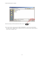
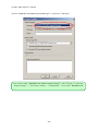
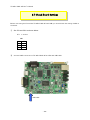
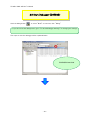
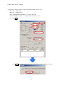
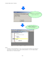
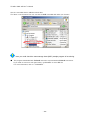
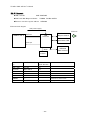
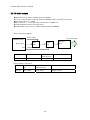
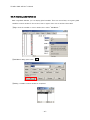
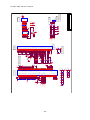
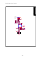
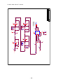
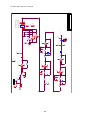
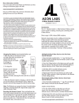
1
User’s Manual
TK-850/JH3U-SP
Date published: November 2008
Rev. 1.0
© TESSERA TECHNOLOGY INC. 2008
Printed in Japan
TK-850/JH3U-SP User’s Manual
Windows and Windows XP are registered trademarks or trademarks of Microsoft Corporation in the United States and/or
other countries.
・The information is subject to change without notice.
・No part of this document may be copied or reproduced in any form or by any means without prior written consent
of TESSERA TECHNOLOGY INC.. TESSERA TECHNOLOGY INC. assumes no responsibility for any errors that
may appear in this document.
・TESSERA TECHNOLOGY INC. does not assume any liability for infringement of patents, copyrights or other
intellectual property rights of third parties by or arising from the use of TESSERA TECHNOLOGY INC. products
listed in this document or any other liability arising from the use of such products. No license, express, implied or
otherwise, is granted under any patents, copyrights or other intellectual property rights of TESSERA
TECHNOLOGY INC. or others.
・Descriptions of circuits, software and other related information in this document are provided for illustrative
purposes in semiconductor product operation and application examples. The incorporation of these circuits,
software and information in the design of a customer's equipment shall be done under the full responsibility of the
customer. TESSERA TECHNOLOGY INC. assumes no responsibility for any losses incurred by customers or third
parties arising from the use of these circuits, software and information.
CAUTION
・Do not give any physical damage to this equipment such as dropping
・Do not superimpose voltage to this equipment.
・Do not use this equipment with the temperature below 0℃ or over 40℃.
・Make sure the USB cables are properly connected.
・Do not bend or stretch the USB cables.
・Keep this equipment away from water.
・Take extra care to electric shock.
・This equipment should be handled like a CMOS semiconductor device. The user must take all precautions to
avoid build-up of static electricity while working with this equipment.
・All test and measurement tool including the workbench must be grounded.
・The user/operator must be grounded using the wrist strap.
・The connectors and/or device pins should not be touched with bare hands.
-2-
TK-850/JH3U-SP User’s Manual
Contents
CHAPTER 1 PREPARATION.....................................................................................................................................................8
1.1 Development Tools / Software..............................................................................................................................9
1.2 Installation of Development Tools ..................................................................................................................... 10
1.2.1 Installation Package .................................................................................................................................. 10
1.2.2 Installation of Development Tools....................................................................................................... 10
1.3 Sample Programs...................................................................................................................................................... 15
1.3.1 Preparation of Sample Programs......................................................................................................... 15
1.3.2 Overview of Sample Programs ............................................................................................................. 18
1.4 Installation of USB Driver ..................................................................................................................................... 19
1.4.1 Installation on Windows XP.................................................................................................................... 20
1.4.2 Installation on Windows 2000 ................................................................................................................ 23
1.4.3 Completion of USB Driver Installation............................................................................................... 26
CHAPTER 2 EXPERIENCES................................................................................................................................................... 27
2.1 Start PM+ .................................................................................................................................................................... 29
2.2 What is PM+................................................................................................................................................................ 30
2.3 Load Workspace (project) ..................................................................................................................................... 32
2.4 Set Options................................................................................................................................................................. 34
2.4.1 "Extend" Tab............................................................................................................................................... 34
2.4.2 “Preprocessor” Tab ................................................................................................................................. 35
2.5 Create Load Module Files ..................................................................................................................................... 36
2.6 Check Debugger Settings...................................................................................................................................... 38
2.7 Check Board Settings............................................................................................................................................. 40
2.8 Start Debugger (ID850QB).................................................................................................................................... 41
2.9 Run Programs............................................................................................................................................................. 44
2.10 Stop Programs ........................................................................................................................................................ 47
2.11 Close Debugger (ID850QB) ................................................................................................................................ 48
2.12 Quit PM+.................................................................................................................................................................... 49
CHAPTER 3 HARDWARE SPECIFICATIONS .................................................................................................................. 50
3.1 Connecter Layout..................................................................................................................................................... 51
3.2 Function Layout ........................................................................................................................................................ 52
3.3 Hardware Functions................................................................................................................................................. 53
3.3.1 SW1.................................................................................................................................................................. 53
3.3.2 SW2 (RESET SW)....................................................................................................................................... 54
3.3.3 SW3 (INTP12) .............................................................................................................................................. 54
3.3.4 SW4 (INTP13) .............................................................................................................................................. 54
3.3.5 LED1................................................................................................................................................................ 55
3.3.6 LED2 (POWER) ........................................................................................................................................... 55
3.3.7 U20 (for no LCD version) ....................................................................................................................... 55
3.3.8 JP1 .................................................................................................................................................................. 56
-3-
TK-850/JH3U-SP User’s Manual
3.3.9 JP2 .................................................................................................................................................................. 56
3.3.10 CN1 ............................................................................................................................................................... 56
3.3.11 CN2 ............................................................................................................................................................... 56
3.3.12 CN4 ............................................................................................................................................................... 56
3.3.13 CN7 ............................................................................................................................................................... 56
3.3.14 CN8 ............................................................................................................................................................... 57
3.3.15 CN9 ............................................................................................................................................................... 57
3.3.16 J1................................................................................................................................................................... 57
3.3.17 NWIRE1 Connector ................................................................................................................................. 57
3.3.18 USB1 Connecter...................................................................................................................................... 57
3.3.19 USB2 Connecter...................................................................................................................................... 57
3.3.20 USB3 Connecter...................................................................................................................................... 57
3.3.21 DSUB1 Connecter................................................................................................................................... 58
3.3.22 U24 (IrDA Infrared communication module).................................................................................. 58
3.3.23 VR1................................................................................................................................................................ 58
3.4 solder-short pad label............................................................................................................................................. 59
3.5 Explanation of unit ................................................................................................................................................... 60
3.5.1 USB function ............................................................................................................................................... 60
3.5.2 USB Host ...................................................................................................................................................... 61
3.5.3 IrDA infrared communication................................................................................................................. 62
3.5.4 Ethernet......................................................................................................................................................... 63
3.5.5 Touch panel LCD (LCD version only) ................................................................................................ 64
3.5.6 SRAM.............................................................................................................................................................. 65
3.5.7 External bus interface.............................................................................................................................. 66
1.1. External bus I/F devices ...................................................................................................................................... 66
1.2. Address mapping...................................................................................................................................................... 66
1.3. External memory address area........................................................................................................................... 66
3.5.8 External connecter.................................................................................................................................... 67
3.5.9 Audio input.................................................................................................................................................... 69
3.5.10 Audio output.............................................................................................................................................. 70
3.5.11 RS-232C ..................................................................................................................................................... 71
CHAPTER 4 TROUBLESHOOTING..................................................................................................................................... 72
4.1 If you cannot find USB driver when you connect PC to the kit............................................................ 72
4.2 Error when you start the debugger ................................................................................................................... 72
4.2.1 "Can not communicate with Emulator..." (F0100 or A0109) .................................................... 72
4.2.2 "Incorrect ID Code." (Ff603) ................................................................................................................ 73
4.3 Monitor memory cannot be accessed. (F0c72) ............................................................................................ 73
CHAPTER 5 OTHER INFORMATION.................................................................................................................................. 74
5.1 Create a new workspace ....................................................................................................................................... 75
5.2 Register additional source file ............................................................................................................................. 83
5.3 Debugger tips ............................................................................................................................................................. 85
-4-
TK-850/JH3U-SP User’s Manual
5.3.1 Change display of buttons...................................................................................................................... 85
5.3.2 Display source list and function list ................................................................................................... 85
5.3.3 Set/delete breakpoints............................................................................................................................ 86
5.3.4 Display global variables............................................................................................................................ 87
5.3.5 Display local variables.............................................................................................................................. 88
5.3.6 Display memory and SFR contents .................................................................................................... 88
5.4 WriteEZ1....................................................................................................................................................................... 89
5.5 Circuit diagram........................................................................................................................................................... 94
-5-
TK-850/JH3U-SP User’s Manual
Introduction
TK-850/JH3U-SP is the evaluation kit for development using "V850ES/JH3-U", NEC Electronics 32bit
all flash microcontroller.
The user only needs to install the development tools and USB driver, and connect the host machine with
the target board to start the code development, build, monitoring the output, and debugging code.
(This demonstration kit uses the on-chip debug feature from the microcontroller itself, without emulator
connection)
Configuration for Debugging
-6-
TK-850/JH3U-SP User’s Manual
Overview
This manual consists of the following contents.
Read chapter 1 and 2 first for installing the development tools and using the sample
programs.
Read chapter 3-5 for customizing the sample programs and the hardware.
Chapter 1:
Chapter 2:
Chapter 3:
Chapter 4:
Chapter 5:
Preparations
Install the development tools
Experiences
Experience the basic operations of integrated development environment
(PM+) and integrated debugger (ID850QB) with using sample programs.
Hardware Specifications
Explain the hardware of TK-850/JH3U-SP
Troubleshooting
Describe how to solve troubles you may face, such as errors when
starting the integrated debugger (ID850QB)
Other Information
Introduce other information, such as how to create a new workspace
(project) on integrated development environment (PM+), how to register
additional source file, and some useful tips of the integrated debugger.
The circuit diagrams of demonstration kit are included in this chapter.
Reader
This manual is intended for development engineers who wish to become familiar with the
development tools for the V850.
It is assumed that the readers have been familiar with basics of microcontrollers, C and
Assembler languages, and the WindowsTM operating system.
Purpose
This manual is intended to give users an understanding of the features, hardware
configurations, development tools for the V850.
-7-
TK-850/JH3U-SP User’s Manual
CHAPTER 1 Preparation
This
-
chapter describes following topics:
Overview and installation of development tools
Installation of development tools
Overview and preparation of sample programs
Users can experience the development flow such as coding, build, debugging, and test, by using the
development tools bundled with TK-850/JH3U-SP.
-8-
TK-850/JH3U-SP User’s Manual
1.1 Development Tools / Software
● Device file DF703771 V1.00
A device file contains device specific information. So, users need a device file to use the
development tools.
● Integrated Development Environment (IDE) PM+ V6.31
The IDE works on Windows operation system.
Users can develop a system efficiently by using the editor with idea processor function,
compiler, and debugger.
● C Compiler CA850 W3.20 (code size limited version)
C compiler for the V850 microcontrollers. The object code size is limited to 128 Kbyte.
This compiles C code for V850 and ANSI-C code program into assembler code.
This produces object code and linker.
● V850 Integrated Debugger ID850QB V3.50
This is the tool for debugging the object program generated by C compiler and assembler. The
debugger enables to do C source level debugging. With the debugger, you can debug the code
easily and efficiently by refering and changing variables, using step-in debuging function, and
so on.
● Built-in Flash Memory Writing Program WriteEZ1
This is the Windows software to write programs on built-in flash memory.
By connecting TK-850/JH3U-SP and PC with bundled USB cable, you can write/delete
programs on the built-in flash memory.
● Sample program
The explanation uses Mass storage class (MSC) sample program in user's manual.
-9-
TK-850/JH3U-SP User’s Manual
1.2 Installation of Development Tools
1.2.1 Installation Package
The attached CD-ROM includes the development tools and documentations. Users can use the installer
to install those development tools and documentations.
1.2.2 Installation of Development Tools
① Please insert the CD-ROM in the drive. The installer will show up automatically.
If it does not start automatically, please initiate it by double clicking the
SETUP.EXE.
<1> Readme First
The contents of the CD-ROM, and some notes are available.
Please read it at first.
<2> Install…
Click “Install” to start installation of development tools.
For details, please refer to the next section.
- 10 -
TK-850/JH3U-SP User’s Manual
<3> Documents
Manuals of development tools and the evaluation kit are available in PDF files.
When this button is clicked, the WWW browser will start. Adobe® Acrobat® Reader is available in the
CD-ROM.
<4> Sample Program
Click this button to start the WWW browser for the sample program and the tutorial.
<5> Link to NEC Electronics Microcontrollers
Click this button to start the WWW browser display the link to the NEC Electronics Microcontroller
web site (http://www.necel.com/micro/index_e.html)
The NEC Electronics Microcontroller web page provides with the latest product/tool information
and FAQs.
<6> Exit
Terminate the setup.
② Click the "Install"
- 11 -
TK-850/JH3U-SP User’s Manual
③ "Tool Installer" dialog box is opened.
Select products that you need to install.
(as default, all the products that you need to use the TK-850/JH3U-SP are selected.)
"Explain" area displays an explanation of the selected product.
To change the installation destination, click Browse… .
When all the settings are completed, click
Install…
.
* In this document, it is assumed that users install the programs under "NEC Electronics Tools"
directory (default installation directory). Users can find the tools by selecting “Start Menu” ->
"Programs" -> "NEC Electronics Tools".
④ Click
OK
when "Install" comfirmation dialog box is opened.
- 12 -
TK-850/JH3U-SP User’s Manual
⑤ Read "software license agreement" and click
To stop the installation, click No .
Yes
⑥ Enter the product ID, and click Next .
* The product ID is available on the other sheet.
⑦ It starts copying the files.
- 13 -
for continuing the installation.
TK-850/JH3U-SP User’s Manual
⑧ If the “install Wizard :Kind of File” dialog displayed, Select ”Device File For V850ES/JH3-U”.
Click OK .
⑨ When the installation is completed, the following dialog opens.
Click OK .
Notes on the installation authority
To install this tool in Windows 2000 or XP, the authority of an administrator is necessary. Therefore,
please login as an administrator.
Notes on the install-directory
Please do not use 2-byte characters, such as umlaut in the directory name, where the product is to be
installed.
Note on the version of Windows
If the language of the Windows is not English, a file transfer error during installation might be observed.
In this case, please abort the installation in the language, and re-install it in an English version of
Windows.
The identical problem may be observed, if a language other than English is specified as the system
language in the “Regional Settings Properties” tab.
Limitation
Assembler RA850 and C compiler CA850 limit the object size to 128Kbyte.
- 14 -
TK-850/JH3U-SP User’s Manual
1.3 Sample Programs
This section explains the overview and preparation of sample programs.
1.3.1 Preparation of Sample Programs
① Insert the CD-ROM disk in the CD-ROM drive of your PC. The [NEC Electronics Microprocessor
Development Tools Setup] screen automatically appears.(if this screen does not appear automatically,
start setup.exe from Explorer. etc.)
② Press the
Sample Program
button to start the WWW browser.
- 15 -
TK-850/JH3U-SP User’s Manual
③ Click the “Mass Storage Class Sample Program MSC Sample Driver ” link , the following download
confimation window appears.
④ Click the
Save
butten.
- 16 -
TK-850/JH3U-SP User’s Manual
⑤ After specifying the download destination folder,click the
Save
button.
⑥ The self-extraction sample program (JH3U_STORAGE.EXE) is copied to the specified folder.
The folder that the “TK850” folder is made when this file is executed, and the sample program is
stored under the”TK850” folder.
- 17 -
TK-850/JH3U-SP User’s Manual
1.3.2 Overview of Sample Programs
The “Mass Storage Class Sample Program MSC Sample Driver” consist of following folders.
TK850
JH3U_STORAGE
include
NEC_Project
src
Include files
Project files for NEC compiler
Source files
- 18 -
TK-850/JH3U-SP User’s Manual
1.4 Installation of USB Driver
"NEC Electronics Starter Kit Virtual UART" USB driver must be installed on PC before you start using
the TK-850/JH3U-SP.
Please, follow the instruction below to install the driver.
"Starter Kit USB Driver" must be installed on the PC. If not, please refer to "1.2 Installation of
Development Tools" to install the driver first.
CAUTION:
Do not use a USB hub for connecting TK-850
First, connect the TK-850 to PC with USB.
USB cable
Depending on the version of Windows OS, the installation will be differed. Please check your
Windows version, and follow the instructions
- Windows XP
-> "1.4.1 Installation on Windows XP"
- Windows 2000 -> "1.4.2 Installation on Windows 2000"
After the installation, go to "1.4.3 Completion of USB Driver Installation"
8
- 19 -
TK-850/JH3U-SP User’s Manual
1.4.1 Installation on Windows XP
1. Once the TK-850/JH3U-SP is connected with USB, the "Found New Hardware Wizard" will be
started.
Select "No, not this time" and click Next > .
Select "No, not this time"
Click "Next"
2.
Select "Install from a list or specific location" and click
Next >
.
Select "Install from a list or specific
location"
Click "Next"
- 20 -
TK-850/JH3U-SP User’s Manual
3.
Select "Search for the best driver in these locations.", check "Include this location in the search:",
and then click "Browse..." to select the driver directory path. The path should be "C:\Program
Files\NEC Electronics Tools\TK-driver" as default installation. If the installation directory is not
default, then select "TK-driver" under the installation directory.
Click Next > .
Select the driver directory
Click "Next"
4.
If the following dialog is opened, click
Continue Anyway
.
Click "Continue Anyway"
- 21 -
TK-850/JH3U-SP User’s Manual
5.
The installation of "NEC Electronics Starter Kit Virtual UART" driver is completed.
Click Finish .
Click "Finish"
6.
Go to "1.4.3 Completion of USB Driver Installation".
- 22 -
TK-850/JH3U-SP User’s Manual
1.4.2 Installation on Windows 2000
1. Once the TK-850/JH3U-SP is connected with USB, the "Found New Hardware Wizard" will be
started.
Select "No, not this time" and click Next > .
Click "Next"
2.
Select "Search for a suitable driver for my device".
Click Next > .
Select "Search for a suitable driver for my
device"
Click "Next"
- 23 -
TK-850/JH3U-SP User’s Manual
3.
Select "Specify a location".
Click Next > .
Select "Specify a location"
Click "Next"
4.
Select the driver directory path. The path should be "C:\Program Files\NEC Electronics
Tools\TK-driver" as default installation.
If the installation directory is not default, then select "TK-driver" under the installation directory.
Click OK .
Click "OK"
Select the driver directory
- 24 -
TK-850/JH3U-SP User’s Manual
5.
Click
Next >
.
Click "Next"
6.
The installation of "NEC Electronics Starter Kit Virtual UART" driver is completed.
Click Finish .
Click "Finish"
7.
Go to "1.4.3 Completion of USB Driver Installation".
- 25 -
TK-850/JH3U-SP User’s Manual
1.4.3 Completion of USB Driver Installation
Confirm the USB driver is installed on PC.
Start "Device Manager", and find "NEC Electronics Starter Kit Virtual UART" (without "?" mark) under
the "Ports (COM & LPT)".
Device Manager
Find "NEC Electronics Starter Kit
Virtual UART (COMx)"
The screen above shows that the COM port number is "COM8". If ID850QB is not in use, you can use
this port number for connecting TK-850/JH3U-SP.
When you change the USB port connection, the COM port number will be changed as well.
CAUTION
・Do not do “Hardware Modification Scan” when you communicate with the target device.
- 26 -
TK-850/JH3U-SP User’s Manual
CHAPTER 2 Experiences
In this chapter, you will experience how to use the development tools with using the sample programs.
The development tools are :
- Integrated Development Environment (IDE), PM+
- Integrated Debugger, ID850QB
You will use the programs that you prepared in "1.3 Sample Programs", as the sample programs for
TK-850/JH3U-SP
You will be able to understand how to use the development tools and the concept of project files which
you need for producing application programs.
- 27 -
TK-850/JH3U-SP User’s Manual
The overall steps are as follows:
2.1 Start PM+
2.3 Load Workspace
2.4 Set Linker Options
2.5 Set Compiler Options
2.6 Create Load Module Files
2.7 Check Debugger Settings
2.8 Check Board Settings
Run Programs
2.9 Start Debugger
2.10 Run Programs
2.11 Stop Programs
2.12 Close Debugger
2.13 Quit PM+
- 28 -
TK-850/JH3U-SP User’s Manual
2.1 Start PM+
Let's start using the development tools.
First, start the PM+
Select "Windows Start Menu" -> "Program" -> "NEC Electronics Tools" -> "PM+ V6.31".
PM+ starts up
- 29 -
TK-850/JH3U-SP User’s Manual
2.2 What is PM+
In PM+, application programs and environment setting are handled as a single project, and series of
actions such as program creation using the editor, source management, build, and debugging are
managed.
Also, one of more project files is managed together as a workspace.
Menu bar
Project Window
Project window
Tool bar
Output Window
A window in which project names, source files, and include file are displayed using a tree
structure.
Output window
A window in which the build execution status is displayed.
For details regarding menu bars and tool bars, refer to "Help" menu in PM+.
"Help" on menu bar , then "PM+ Help"
- 30 -
TK-850/JH3U-SP User’s Manual
What is a project?
A project is the unit that is managed by PM+. A project refers to an application system and environment
development based on PM+.
PM+ saves project information in a "project file".
What is a project file?
A project file contains project information that includes the source files, device name, tool options for compiling,
editor, and debugger information.
The file name format is "xxxxx.prj".
Project files are created in the directory you specifies when you create a new workspace.
What is a project group?
A project group is a group comprised of a number of projects in an application system.
The target device of each project must be the same within a project group.
What is a workspace?
A workspace is the unit used to manage all the projects and project group required for one application system.
A workspace file contains one or more project files.
The file name format is "xxxxx.prw".
- 31 -
TK-850/JH3U-SP User’s Manual
2.3 Load Workspace (project)
In this section, you will use the workspace that you created in "1.3 Sample Programs"
For creating a new workspace, refer to "Chapter 5 Other Information".
The workspace has information about the build environment for the sample programs.
Select "File" on menu bar and "Open Workspace…". Then, select "V850JH3U_Fnc_MSC.prw " under the
directory ”C:\TK850\JH3U_STORAGE\NEC_project".
Select the directory that
contains the sample
programs.
Select "V850JH3U_Fnc_MSC.prw", then click
- 32 -
Open
.
TK-850/JH3U-SP User’s Manual
Workspace name: "V850JH3U_Fnc_MSC.prw
Load the workspace file
"V850JH3U_Fnc_MSC.prw"
Project group
Project
The workspace file "V850JH3U_Fnc_MSC.prw" contains one project called "V850JH3U_Fnc_MSC". You
will use this project "V850JH3U_Fnc_MSC".
CAUTION:
Please ignore when you get a prompt saying "files could not be found". This may occurred when
the installation directory is not a default.
- 33 -
TK-850/JH3U-SP User’s Manual
2.4 Set Options
The compiler options have been set by project file. However, because some compiler options are useful,
following two settings are covered specifically in this section.
- Enable C++ comments
- On-chip debug (Disable/Enable, security ID)
Select "Tools" on menu bar, then "Compiler Common options".
2.4.1 "Extend" Tab
Select "Device" tab on "Compiler Common Options" window, and check following settings.
Set the security ID. The security ID is a specific ID code (10 bytes) used for the authentication
when the debugger is starting. The security ID is stored at the address 70H-79H in the
microcontroller built-in flash memory. The security ID in the flash memory and the ID entered in the
configuration dialog are compared when the debugger is starting. When the ID does not match, the
debugger cannot be started. Therefore, it is useful to protect the program data in the memory from
others.
If you do not need to care about the security, it is recommended to enter
"FFFFFFFFFFFFFFFFFFFF". (When you erase the data in the flash memory, the ID is set to this
value.)
- 34 -
TK-850/JH3U-SP User’s Manual
If you forgot the security ID code stored in the address 70H-79H, the debugger (ID850QB) will not
be able to start.
In this case, you need to use "WriteEZ1" to erase the built-in flash memory. By erasing the flash
memory, the security ID is set to "FFFFFFFFFFFFFFFFFFFF".
For details, refer to "5.4 WriteEZ1".
2.4.2 “Preprocessor” Tab
Select "Tool" on menu bar in PM+, then "Compiler Options...".
Select "Preprocessor" tab, and check "Use C++ Style Comment".
This setting allow you to use the C++ comment using "//".
It is useful feature when editing programs.
- 35 -
TK-850/JH3U-SP User’s Manual
2.5 Create Load Module Files
After developing the source code, you have to create load module files by compiling, assembling, and
linking. This process is called build.
Click the build button
, or select "Build" on menu bar, then "Build".
Build has been completed successfully.
- 36 -
TK-850/JH3U-SP User’s Manual
What is build?
Build is a function that creates an executable file from source files in a project.
PM+ automatically performs compiling, assembling, linking, and other processing actions.
To reduce the time for the build, PM+ detects and compiles/assembles only the files that have been
updated from the previous build process.
What is rebuild?
Build compiles and assembles only the source files that have been updated from the previous
time, whereas rebuild compiles and assembles all the source files.
When setting, such as compiler options, have been changed, you must rebuild instead of build.
- 37 -
TK-850/JH3U-SP User’s Manual
2.6 Check Debugger Settings
After the build, you should configure the debugger settings.
The debugger settings have been set by the project file as well. However, because those settings are
important for debugging, some settings are covered in this section.
Select "Tools" on menu bar, then "Debugger Setting...".
- 38 -
TK-850/JH3U-SP User’s Manual
Check if "ID850QB V3.50 V850 Integrated Debugger" is selected on "Debugger".
If you cannot select "ID850QB V3.50 V850 Integrated Debugger", select "Project" on menu bar,
"Project settings" -> "Tool version settings" -> "Detailsetting" -> then select "ID850QB V3.50".
- 39 -
TK-850/JH3U-SP User’s Manual
2.7 Check Board Settings
Before connecting the PC and the TK-850/JH3U-SP with USB, you should check the setting of SW1 on
the board.
①
Set JP2 and SW1 as shown below.
JP1 :1-2 short
SW1
Bit1
Bit2
Bit3
Bit4
②
OFF
ON
ON
ON
Connect USB1 connecter on TK-850/JH3U-SP and PC with USB cable.
USB cable
- 40 -
TK-850/JH3U-SP User’s Manual
2.8 Start Debugger (ID850QB)
Click the debug button
, or select "Build" on menu bar, then "Debug".
If you do not see the debug button, go to "2.7 Check Debugger Settings" for changing the settings.
The steps to start the debugger will be explained below.
ID850QB is launched
- 41 -
TK-850/JH3U-SP User’s Manual
"Configuration" dialog is opened. Follow the settings below and click "OK".
・Enter "6" in "Main OSC"
・Enter “8” in "Multiply rate"
・Enter "FFFFFFFFFFFFFFFFFFFF" (F x 20) in "ID Code".
・Select "UARTD0" in "Port" at "Target Device Connection" area
then click
Click
OK
.
Yes
when the confirmation dialog for downloading load module file is opened.
- 42 -
TK-850/JH3U-SP User’s Manual
ID850QB starts and downloading the
program to flash memory.
When the download is
completed, the source code
will be displayed
NOTE:
Completion of the download does not mean running the programs. Therefore, even though you
press switch on the board, it does not make anything happened. To run the sample program
demonstration, see "2.9 Run Programs".
- 43 -
TK-850/JH3U-SP User’s Manual
2.9 Run Programs
Now, you are ready to run the program.
Click the restart button
, or select "Run" on menu bar, then "Restart".
The sample program runs.
Run the sample program
When programs are running, the status bar will be red.
- 44 -
TK-850/JH3U-SP User’s Manual
Connect USB3 and PC with another USB cable while USB1 is still connected.
USB cable
When it is connected to PC, the driver is automatically installed. It is detected as "NEC corp
TK-850JG3-H/JH3- USB Device" under disk drive.
- 45 -
TK-850/JH3U-SP User’s Manual
Also, the removable disk is added as a disk drive.
This drive is not formatted. You can use this as 24KB removable disk when you format it.
Now you could check the mass storage class (MSC) sample program is functioning.
●
The program downloaded with ID850QB cannot be executed without ID850QB connection.
If you need to execute it with stand-alone, use WriteEZ1 to write HEX file.
For more information, refer to "5.4 WriteEZ1".
- 46 -
TK-850/JH3U-SP User’s Manual
2.10 Stop Programs
Now, you are going to stop the program.
Click the stop button
, or select "Run" on menu bar, then "Stop".
Stop the program
When the program stops, the status bar changes back to the original color.
- 47 -
TK-850/JH3U-SP User’s Manual
2.11 Close Debugger (ID850QB)
Select "File" on menu bar, then "Exit".
The exit confirmation dialog is displayed.
If you click
Yes
, it saves the settings in the project file, and then closes the ID850QB. It is
recommended to save the settings as it saves the window you used, window size, layout, etc.
If you click
No
, it does not save the settings and closes the ID850QB.
- 48 -
TK-850/JH3U-SP User’s Manual
2.12 Quit PM+
Select "File" on menu bar, then "Exit PM+".
PM+ is closed.
The experiences section ends now.
You can find more information how to use the development tool and information about other useful
features in "Chapter 5 Other Information".
- 49 -
TK-850/JH3U-SP User’s Manual
CHAPTER 3 Hardware Specifications
In this chapter, the hardware of TK-850/JH3U-SP will be explained.
Microcontroller
Clock
Interface
Other unit
Dimension
Power supply voltage
μPD70F3769 ※V850ES/JH3-U
External main system clock: 48MHz (6MHz x8)
Sub-clock: 32.768KHz
USB (A receptacle) x1
USB (MINI B connecter) x2
Connecter for N-Wire (For KEL connecter)
Connecter for MINICUBE2
(For SICA connecter only pad)
Dsub-9Pin x1
Expansion connector (50Pin)
RJ-45 connecter
IrDA communication interface
Audio input (φ3.5mm monaural jack)
Audio output (φ3.5mm monaural jack)
AC adopter jack (5V)
Touch panel LCD (for LCD version)
7Seg-LED (for no LCD version)
100mm x 136mm
5V
- 50 -
TK-850/JH3U-SP User’s Manual
3.1 Connecter Layout
USB2
DSUB1
USB3
USB1
NWIRE1
CN1
CN2
CN9
- 51 -
CN7
CN4
CN8
TK-850/JH3U-SP User’s Manual
3.2 Function Layout
LED1
SW2
U24
JP2
SW1 LED2
U20
- 52 -
SW3
SW4
VR1
JP1
TK-850/JH3U-SP User’s Manual
3.3 Hardware Functions
3.3.1 SW1
The bit 1-4 on SW1 are for mode settings, Bit5-8 of SW1 are connected to ”P78/ANI8”~”
P711/ANI11” for general-purpose input port.
● For the use of ID850QB, use following settings.
SW1
Bit1
Bit2
Bit3
Bit4
*
OFF
ON
ON
ON
When ID850QB is used, these terminals cannot be used because it communicates with the host
machine by using and the terminal P30 and P31.
● Please change to the following settings when writing it in the flash memory with built-in CPU by using
WriteEZ1. (The hardware of WriteEZ1 is built into TK-850/JH3U-SP.)
SW1
Bit1
Bit2
Bit3
Bit4
OFF
ON
ON
ON
● To run the programs stored in built-in flash memory by WriteEZ1, use following settings and re-supply
power.
SW1
Bit1
Bit2
Bit3
Bit4
OFF
OFF
OFF
OFF ※
※If you need to use USB1 as virtual serial port, set Bit4 to ON.
- 53 -
TK-850/JH3U-SP User’s Manual
● Please change to the following settings when you connect N-Wire emulator.
SW1
Bit1
Bit2
Bit3
Bit4
OFF
OFF
OFF
OFF
● Please change to the following settings when you use virtual serial COM port.
SW1
Bit1
Bit2
Bit3
Bit4
OFF
OFF
OFF
ON ※
※If you need to use USB1 as virtual serial port, set Bit4 to ON.
● Bit5-8 are connected to following CPU pins.
As they are connected to pull-up resister, "ON" means "Low" and "OFF" means "High".
SW1
Bit5
Bit6
Bit7
Bit8
P78
P79
P710
P711
3.3.2 SW2 (RESET SW)
This is the reset switch. You can reset the microcontroller by pressing this switch.
3.3.3 SW3 (INTP12)
SW3 is the push switch connected to ”P98/SOF1/INTP12/A8” pin in CPU. There are connecting to
pull-up resister. When the switch is pushed down, it sends the signal of "Low".
3.3.4 SW4 (INTP13)
SW4 is the push switch connected to ”P99/SCKF1/INTP13/A9” pin in CPU. There are connecting to
pull-up resister. When the switch is pushed down, it sends the signal of "Low".
- 54 -
TK-850/JH3U-SP User’s Manual
3.3.5 LED1
This is the Bus Power LED for USB2 connecter. It is lighted when USB2 connecter gets power supply.
3.3.6 LED2 (POWER)
This is the POWER LED. It is lighted when it gets power supply.
3.3.7 U20 (for no LCD version)
This is the 7Seg-LED.
7Seg-LED display can be changed by accessing the address between 600000h and 6FFFFFh.
U20
Bit0
Bit5
Bit1
Bit6
Bit4
Bit2
Bit3
0
1
2
3
4
Bit7
Example of displayed figure and set data.
0xC0
5
0x92
0xF9
0xA4
0xB0
0x99
6
7
8
9
- 55 -
0x83
0xf8
0x80
0x98
TK-850/JH3U-SP User’s Manual
3.3.8 JP1
JP1 is a jumper short pin to select power supply for CN8 MIC INPUT.
Set the jumper to short when you connect electret condenser microphone.
3.3.9 JP2
JP2 is a jumper short pin to select power supply.
1-2 short
3-4 short
5-6 short
Use power supply from USB1 connecter.
Use power supply from USB3 connecter.
Use power supply from AC adapter connected to CN9.
Caution
When you use USB host connection with USB2 or use LCD display, you must use power supply from
AC adapter.
3.3.10 CN1
CN1 is an extended connecter.
FX8C-100P-SV6 connecter by Hirose Electric Co., LTD. is mounted.
3.3.11 CN2
CN2 is a connecter pad for MINICUBE2 connection (connecter is not mounted).
3.3.12 CN4
CN4 is RJ-45 connecter socket for Ethernet connection.
3.3.13 CN7
CN7 is an audio output connecter.
P10/ANO0 signal output is output through low-pass filter.
Connect φ3.5mm mini plug.
- 56 -
TK-850/JH3U-SP User’s Manual
3.3.14 CN8
CN8 is an audio input connecter.
P72/ANI2 inputs signal through low-pass filter.
Connect φ3.5mm mini plug.
3.3.15 CN9
CN4 is the power supply connecter of the AC adaptor.
You can supply the power by setting the JP2 to 5-6 short and connect AC adapter.
3.3.16 J1
This is the connector for external power supply. (DC5V)
3.3.17 NWIRE1 Connector
These are connector for N-Wire emulator.
It can connect N-Wire emulator of IE-V850E1-CD-NW etc.
8831E-026-170L-F connecter by KEL Corp. is mounted.
3.3.18 USB1 Connecter
This is a connecter for on-chip debug and flash memory writing.
This can be used as a virtual serial COM port by setting SW1.
3.3.19 USB2 Connecter
This is a connecter for USB host connection.
Caution
When you use USB host connection with USB2 or use LCD display, you must use power supply from
AC adapter.
3.3.20 USB3 Connecter
This is a connecter for USB function connection.
- 57 -
TK-850/JH3U-SP User’s Manual
3.3.21 DSUB1 Connecter
This is a Dsub-9Pin connecter for RS-232C communication.
RS-232C communication can be made with using P90/TXDC1 and P91/RXDC1.
3.3.22 U24 (IrDA Infrared communication module)
This is an IrDA infrared communication module.
3.3.23 VR1
This is an initial level volume control for the audio input (CN8) signal.
- 58 -
TK-850/JH3U-SP User’s Manual
3.4 solder-short pad label
When using an external connector without using a circuit on board, in order to separate a circuit on
board, the terminal of CPU can be customized by making the pad for solder short opening.
Pad for solder-short has shape like the figure below.
When you make an open circuit, cut the narrow part of the Pad with a knife.
To make short circuit, join the separated Pad with a soldering iron etc.
Solder-short pad
(opened shape)
Solder-short
pad name
Solder-short pad
Shorted shape
State when
shipping it
T_RESET
Short
FLMD0
Short
USB_P1
Open
TXDC1
Short
RXDC1
Short
P1
Short
Connection
Connect reset IC to T_RESET signal
Open when reset IC is not in use.
FLMD0 to P37 on CPU
Short when built-in flash memory is rewritten by self
USB Host bus power switch output
Short when you set maximum bus power output
current to 1A.
Connect P90/TXDC1 and RS-232C driver.
Open when you use it not for RS-232C.
Connect P91/RXDC1 and RS-232C driver.
Open when you use it not for RS-232C.
Connect RTC and CTS of RS-232C.
Open when RTC and CTS should be disconnected.
P2
Short
VOLUME1
Short
Connect DSR and DTR of RS-232C.
Open when DSR and DTR should be disconnected.
Audio output volume signal and P11/ANO1
Open when P11/ANO1 should be disconnected.
- 59 -
TK-850/JH3U-SP User’s Manual
3.5 Explanation of unit
3.5.1 USB function
zUSB connecter
Mini B receptacle
USB Function block diagram
3.3V Power supply
V850ES/JH3-U
Power supply
Pull-Up signal
Pull-Up control
USB signal
Pull-up
Circuit
Vbus
USB
Conncter
Pull-up
USB data
V850ES/JH3-U pin
Connecter
UDPF
UDMF
P41/SOF0/RXDC4/SCL01
P42/_SCKF0/INTP10
D+
D-
V850ES/JH3-U
Signal direction
I/O
I/O
Out
In
- 60 -
Note
3.3V 1.5kΩPull-up
D+ Pull-up control
D+ Pull-up signal
USB
TK-850/JH3U-SP User’s Manual
3.5.2 USB Host
zUSB connecter
A receptacle
zWhen you use USB host connection with USB2, you must use power supply from AC adapter for
supplying USB bus power.
USB Host block diagram
5.0V power supply
V850ES/JH3-U
Vbus
Power ON signal
Power supply
Controller
Vbus
power supply
USB
connecter
Vbus
Current fault signal
USB data
V850ES/JH3-U pin
Connecter
D+
D-
V850ES/JH3-U
Signal direction
I/O
I/O
Out
UDPH
UDMH
P34/TIAA10/TOAA10/TO
AA1OFF/INTP09/PPON
P35/TIAA11/TOAA11/RT
C1HZ/OCI
Vbus Power ON
-
In
Vbus Current fault signal
- 61 -
Note
USB
TK-850/JH3U-SP User’s Manual
3.5.3 IrDA infrared communication
zIrDA controller
ITX E-Globaledge LC16MI-0110A
zIrDA module
ROHM RPM971-H14
zIrDA controller register base address 0x400000
IrDA block diagram
3.3V power supply
1.8V power supply
V850ES/JH3-U
EXT bus
IrDA
Controller
IrDA
Module
Interrupt
clock
48MHz
Oscillator
IrDA controller
pin
A0~A7
D0~D7
_RD
_WE
_CS
_INTR
_RESET
XIN/CLK48M
V850ES/JH3-U
pin
A1~A8
AD0~AD7
_RD
_WR1
→
P05/INTP04
→
-
V850ES/JH3-U
Signal direction
Out
I/O
Out
Out
Note
Connect to address decoder
Interrupt to CPU
Connect to reset circuit
Input from shared USB clock
In
-
- 62 -
Ir
Communication
TK-850/JH3U-SP User’s Manual
3.5.4 Ethernet
zLAN controller
ASIX AX88796B
zRJ45 Jack With Magnetic Module
TAIMAG RJLBC-248TA1
zEthernet controller register address 0x500000
Ethernet block diagram
3.3V power supply
Ethernet
V850ES/JH3-U
EXT bus
RJ45 Jack with
Magnetic Module
LAN
Controller
LINK State LED
Speed State LED
Interrupt
Serial
EEPROM
(MAC address)
Clock
25MHz
Oscillator
LAN controller
pin
SA0~SA5
D0~D15
nRD
nWE
nCS
nRESET
IRQ
V850ES/JH3-U pin
A1~A5
AD0~AD15
_RD
_WR1
→
→
P04/INTP03
V850ES/JH3-U
Signal direction
Out
I/O
Out
Out
Note
Connect to address decoder
Connect to reset circuit
Interrupt to CPU
In
- 63 -
TK-850/JH3U-SP User’s Manual
3.5.5 Touch panel LCD (LCD version only)
zLCD panel
CASIO
zLCD controller
Epson
zLCD controller register base address
zLCD controller memory base address
COM50T5117GTC (5.0inch QVGA color)
S1D13A05F00AB00B
0x600000
0x680000
Caution
When you use LCD display, you must use power supply from AC adapter.
Touch Panel LCD block diagram
3.3V power supply
2.5V power supply
V850ES/JH3-U
EXT bus
LCD
controller
Reset circuit
CSI2
A/D Port
Display
data
LCD
panel
Serial communication
Touch panel signal
5.0V power supply
Port output
Back light LED
driver
Enable signal
LCD controller
LCD controller
pin
AB[17:1]
DB[15:0]
CS#
AB0
M/R#
CLKI
RD/WR#
RD#
WE0#
WE1#
WAIT#
RESET#
V850ES/JH3-U pin
A1~A17
AD0~AD15
→
→
A19
CLKOUT
_RD
_RD
_WR0
_WR1
_WAIT
→
V850ES/JH3-U
Signal direction
Out
I/O
Note
Address decode
GND
Out
Out
Out
Out
Out
Out
In
Bus clock
Connect to reset circuit
- 64 -
TK-850/JH3U-SP User’s Manual
Touch panel LCD connection
LCD panel
V850ES/JH3-U pin
Note
P97/SIF1/TIAA20/TOAA20/A7
V850ES/JH3-U
Signal direction
OUT
YU
XR
P96/TIAA21/TOAA21/INTP11/A6
OUT
Output port
YL
A/D in
OUT
A/D in
OUT
A/D input
Output port
A/D input
Output port
CSI
CSI
Out
LCD control
LCD control
LCD control
/RESET
P71/ANI1
P95/TIAA30/TOAA30/A5
P70/ANI0
P94/TIAA31/TOAA31/TENC00/EV
TT00/A4
P23/_SCKF2/KR5/RTP05
P22/SOF2/KR4/RTP04
P21/SIF2/TIAB00/KR3/TOAB00/R
TP03
→
BLON
→
XL
SCL
SI
/ CS
3.5.6 SRAM
z1Mbyte (8Mbit) SRAM is installed.
zSRAM memory base address
0x100000
- 65 -
Output port
Connect to reset
circuit
Back light enable
output
TK-850/JH3U-SP User’s Manual
3.5.7 External bus interface
1.1. External bus I/F devices
Device
IrDA controller
LAN controller
LCD controller
SRAM
Address pin
A0-7
SA0-5
M/R, AB1-17
A0-18
Accessing condition
16bit access
16bit access
16bit access
16bit access
Note
The device is 8bit
A1 is 2Byte pin
AB1 is 2Byte pin
1MByte
1.2. Address mapping
zThe address decoder assigns 4 devices to 010 0000H~01FFFFFH (CS0 area)と 040 0000H~07F
FFFFH (CS2 area).
Adress
Assign
07FFFFF
1MB
0700000
06BFFFF
LCD mem
0680000
1MB
User area
061FFFF
LCD Reg
0600000
1MB
05000FF
Ethernet
0500000
1MB
04001FF
IrDA
0400000
Address Assign
01FFFFF
External 1MB
SRAM
0100000
00FFFFF
Internal
1MB
ROM
0000000
1.3. External memory address area
z070 0000H~07F FFFFH (CS2 area) 1MByte size
z080 0000H~0FF FFFFH (CS3 area) 8MByte size
- 66 -
User area
TK-850/JH3U-SP User’s Manual
3.5.8 External connecter
zYou can connect external bus signals to external devices with external connecter (CN1)
(HIROSE FX8C-100P-SV4)
External conncter block diagram
V850ES/JH3-U
EXT bus
EXT
connecter
Ports
Power
- 67 -
TK-850/JH3U-SP User’s Manual
External connecter connections
No.
1
3
5
7
9
11
13
15
17
19
21
23
25
27
29
31
33
35
37
39
41
43
45
47
49
51
53
55
57
59
61
63
65
67
69
71
73
75
77
79
81
83
85
87
89
91
93
95
97
99
V850ES/JH3-U pin
A0
A1
A2
A3
A4
A5
A6
A7
A8
A9
A10
A11
A12
A13
A14
A15
PCM0/WAIT
PCM1/CLKOUT
CS_USER_n
PCS2/CS2
PCS3/CS3
PCT0/WR0
PCT1/WR1
PCT4/RD
PCT6/ASTB
PDH0/A16
PDH1/A17
PDH2/A18
PDH3/A19
PDH4/A20
PDH5/A21
PDH6/A22
PDH7/A23
PDL0/AD0
PDL1/AD1
PDL2/AD2
PDL3/AD3
PDL4/AD4
PDL5/AD5/FLMD1
PDL6/AD6
PDL7/AD7
PDL8/AD8
PDL9/AD9
PDL10/AD10
PDL11/AD11
PDL12/AD12
PDL13/AD13
PDL14/AD14
PDL15/AD15
PCM2/HLDAK
Bus
●
●
●
●
●
●
●
●
●
●
●
●
●
●
●
●
●
●
●
●
●
●
●
●
●
●
●
●
●
●
●
●
●
●
●
●
●
●
●
●
●
●
●
●
●
●
●
●
●
●
No.
2
4
6
8
10
12
14
16
18
20
22
24
26
28
30
32
34
36
38
40
42
44
46
48
50
52
54
56
58
60
62
64
66
68
70
72
74
76
78
80
82
84
86
88
90
92
94
96
98
100
V850ES/JH3-U pin
PCM3/HLDRQ
P00/INTP00
P01/INTP01
P02/NMI
P11/ANO1
P20/TIAB03/KR2/TOAB03/RTP02
P24/INTP05
P25/INTP06
P32/ASCKC0/SCKF4/TIAA00/TOAA00
P33/TIAA01/TOAA01/RTCDIV/RTCCL
P36/TXDC3/SCL00/UDMARQ0
P37/RXDC3/SDA00/UDMAAK0
P40/SIF0/TXDC4/SDA01
P50/TIAB01/KR0/TOAB01/RTP00/UDMARQ1
P51/TIAB02/KR1/TOAB02/RTP01/UDMAAK1
P60/TOAB1T1/TIAB11/TOAB11
P61/TOAB1B1/TIAB10/TOAB10
P62/TOAB1T2/TIAB12/TOAB12
P63/TOAB1B2/TRGAB1
P64/TOAB1T3/TIAB13/TOAB13
P65/TOAB1B3/EVTB1
P74/ANI4
P75/ANI5
P76/ANI6
P77/ANI7
P90/KR6/TXDC1/SDA02/A0
P91/KR7/RXDC1/SCL02/A1
P92/TENC01/TIT01/TOT01/A2
P93/TECR0/TIT00/TOT00/A3
P94/TIAA31/TOAA31/TENC00/EVTT00/A4
P95/TIAA30/TOAA30/A5
P96/TIAA21/TOAA21/INTP11/A6
P97/SIF1/TIAA20/TOAA20/A7
P914/TIAA51/TOAA51/INTP17/A14
P915/TIAA50/TOAA50/INTP18/A15
RESET
AGND
3.3VAnalog (AVDD)
3.3VDigital (VDD3.3)
3.3VDigital (VDD3.3)
3.3VDigital (VDD3.3)
GND
GND
GND
GND
GND
VDD5V (VDD)
VDD5V (VDD)
VDD5V (VDD)
VDD5V (VDD)
- 68 -
Bus
●
TK-850/JH3U-SP User’s Manual
3.5.9 Audio input
zYou can capture analogue audio signal with the V850ES/JH3-U internal A/D converter.
zMonaural microphone level input.
(Set the JP1 to short when you connect electret condenser microphone.)
zφ3.5mm Monaural mini plug input
zAnti-aliasing filter Fc = 3.6kHz
zFilter structure = Three 2nd order low pass filters (-36dB/oct)
zVariable gain amplifier Micro Chip MCP6S91
Audio input block diagram
Power supply
Microphone input
V850ES/JH3-U
φ3.5mm
jack
Variable gain
amplifier
Volume
A/D input
Anti-aliasing filter
Connecter pin
V850ES/JH3-U pin
Audio Input
P72/ANI2
V850ES/JH3-U
signal direction
A/D input
Note
Preamp、filter, variable gain amp
passed.
Variable gain amplifier connection
Pin
CS
SI
SCK
V850ES/JH3-U pin
P40/SIF0/TXDC4/SDA01
P22/SOF2/KR4/RTP04
P23/_SCKF2/KR5/RTP05
V850ES/JH3-U signal direction
Out
Out
Out
- 69 -
Note
Chip select
TK-850/JH3U-SP User’s Manual
3.5.10 Audio output
zMonaural line level output. (Speaker drive acceptable)
zYou can output analogue audio signal with the V850ES/JH3-U internal D/A converter.
zAnti-aliasing filter Fc = 3.6kHz
zFilter structure = Three 2nd order low pass filters (-36dB/oct)
zφ3.5mm Monaural/stereo mini plug output
zAmplifier With volume control National Semiconductor LM4865M
Audio output block diagram
Power supply
Line level output
V850ES/JH3-U
Amp
Filter
D/A output
P11
φ3.5mm
Jack
Power
Amp
Volume control
Connecter pin
V850ES/JH3-U pin
Audio Output
P10/ANO0
V850ES/JH3-U
signal direction
D/A output
Note
Output to filter circuit
Power amplifier connection
Pin
DC Vol
V850ES/JH3-U
pin
P11/ANO1
V850ES/JH3-U
signal direction
D/A output
- 70 -
Note
Volume control
TK-850/JH3U-SP User’s Manual
3.5.11 RS-232C
zDSUB1 is the RS-232C serial communication connecter
zYou can cut the RS-232C driver output by cutting the solder short pad (TXDC1、RXDC1) for
using the 3.3V level UART communication with external connecter
zRS-232C driver IC MAX3232
zConnecter
D-sub 9Pin plug
RS-232C block diagram
3.3Vpower supply
V850ES/JH3-U
UART
RS-232C
driver
Solder short
pad
Dsub-9Pin
connecter
To external connecter
Driver IC
V850ES/JH3-U pin
TXD
RXD
P90/KR6/TXDC1/SDA02/A0
P91/KR7/RXDC1/SCL02/A1
V850ES/JH3-U
signal direction
Out
In
Note
UARTC1
UARTC1
RS-232C connecter pin connection (D-sub 9Pin plug)
N.C.
1pin
6pin
Connected to Pin4
(* 1)
2pin
RXD
7pin
Connected to Pin8
(*2)
3pin
TXD
8pin
Connected to Pin7
(*2)
4pin
Connected to Pin6
9pin
N.C.
(* 1)
5pin
GND
Shell
N.C.
*1:You can cut the signal connection by cutting the solder short pad “P2”.
*2:You can cut the signal connection by cutting the solder short pad “P1”.
- 71 -
TK-850/JH3U-SP User’s Manual
CHAPTER 4 Troubleshooting
This chapter describes how to solve troubles you may face.
4.1 If you cannot find USB driver when you connect PC to the kit
Check Point 1
If you use USB hub, do not use it. (USB hub is not supported)
Check Point 2
Check if you installed "NEC Electronics Starter Kit Virtual UART Driver" in "1.4 Installation of
USB Driver". If not, install the driver.
Check Point 3
If above 2 check points are confirmed, disconnect the USB cable from PC and re-connect again.
4.2 Error when you start the debugger
There could be several reasons to make errors happen.
The solving processes differ depending on errors. Please check the error message first.
The solving processes for each error are as follows.
4.2.1 "Can not communicate with Emulator..." (F0100 or A0109)
Check Point 1
If you use USB hub, do not use it. (USB hub is not supported)
Check Point 2
Check if the settings of switches on the kit are correct with referring "2.7 Check Board Settings".
Check Point 3
Confirm the USB driver installation with referring to "1.4 Installation of USB Driver".
Check Point 4
If above 3 check points are confirmed, close the debugger and disconnect the USB cable from PC.
Re-connect USB cable properly to both the PC and the kit, and then re-start the debugger.
- 72 -
TK-850/JH3U-SP User’s Manual
4.2.2 "Incorrect ID Code." (Ff603)
This error occurs when the security ID stored on microcontroller built-in flash memory is different
from the ID code you entered at the start of debugger.
Security ID entry area at the start of debugger
Check Point 1
Enter correct security ID and click OK on the configuration window.
Check Point 2
If you forgot the security ID, you have to erase the microcontroller built-in flash memory. Before
erasing, check if you actually set the security ID with referring to "2.5 Set Options". Also
remember the code you set for the security ID.
After this, erase the flash memory with referring to "5.4 WriteEZ1".
4.3 Monitor memory cannot be accessed. (F0c72)
Check Point 1
Check if the settings of switches on the kit are correct with referring "2.7 Check Board Settings".
Check Point 2
Erase the flash memory with referring to "5.4 WriteEZ1".
Check Point 3
If above 2 check points are confirmed, disconnect the USB cable from PC and re-connect again.
And, retry starting the debugger.
- 73 -
TK-850/JH3U-SP User’s Manual
CHAPTER 5 Other Information
This chapter explains some useful operation techniques of development tools and circuit diagram of the
kit for developing of user programs.
5.1 Create a new workspace (project)
5.2 Register additional source file
5.3 Debugger tips
5.4 WriteEZ1
5.5 Circuit diagram
- 74 -
TK-850/JH3U-SP User’s Manual
5.1 Create a new workspace
Now, create a new workspace and project.
PM+ allows you to create a new workspace with following "New WorkSpace" dialog.
Select "File" on PM+ menu bar, then "New Workspace...".
"New WorkSpace" dialog
opens
<Description of items>
Workspace File Name:
-> Specify the name of the workspace file that manages
the project files.
.prw is automatically suffixed as the file type.
A project file (.prj) of the same name is
simultaneously created.
Folder:
-> Specify the folder for saving the workspace file by
writing its absolute path.
This item can be selected from a reference dialog
box by pressing the Browse… button.
Project Group Name:
-> Specify this item if wishing to manage multiple
projects together in function units.
If nothing is specified, this item is the same as the
workspace file name.
Microcontroller Name:
-> Specify the name of the microcontroller to be used.
Device Name:
-> Specify the name of the device to be used.
The concrete information set here is
described on the following pages
- 75 -
TK-850/JH3U-SP User’s Manual
Input the workspace information
setting as follows.
Workspace file name
→ test
Folder
→ C:\TK850\test
Project Group Name
→ (no input)
Microcontroller Name
→ V850
Device Name
→ uPD70F3769
Click
Click
Yes
Next >
button
button
Click
- 76 -
Detail Setting
button
TK-850/JH3U-SP User’s Manual
Set the version of tools as
follows.
CA850:W3.20
ID850QB:V3.50
Select tools as above screenshot, then click
Click
Next >
- 77 -
OK
.
TK-850/JH3U-SP User’s Manual
Select the “Copy and Use the
Sample file”.
Press the Next > button.
Select the “ 32-Register Mode”.
Press the Next > button.
- 78 -
TK-850/JH3U-SP User’s Manual
Select the “Create and Use
the sample file”
Press the Next > button.
Press the Next > button.
- 79 -
TK-850/JH3U-SP User’s Manual
Select the “ID850QB V3.50”
Press the Next > button.
Check the project
information setting
contents.
Press the Finish button.
- 80 -
TK-850/JH3U-SP User’s Manual
The “test” project has
been registered.
This completes workspace and project creation.
Additional source files can be registered at any time thereafter.
For details, refer to “Registering additional source files”.
Next, setup the security ID
In the PM +, [Tool] → [Compiler common Options...] is selected.
- 81 -
TK-850/JH3U-SP User’s Manual
Compiler Common
Options setting is open.
Click the “Device” tab.
The actualities of
"FFFFFFFFFFFFFFFFFFFF"(20 of F)
are taken if there is no problem in the
value of ID in security.
Press the OK button.
Security ID settings are complete
- 82 -
TK-850/JH3U-SP User’s Manual
5.2 Register additional source file
Now, register additional source files.
The following example shows the additional registration of source files “b.c” and “c.c” with source file
“a.c” already registered.
Place the cursor on the source file in the Project window of PM+, and select [Add Source Files…]
displayed in the right-click menu.
Select source files "b.c" and
"c.c", then click Open
Multiple source files can be selected by clicking them with pressing
- 83 -
Ctrl
key.
TK-850/JH3U-SP User’s Manual
Source file "b.c" and
"c.c" are additionally
registered to the project.
- 84 -
TK-850/JH3U-SP User’s Manual
5.3 Debugger tips
This section describes some useful techniques for the debugger (ID850QB).
5.3.1 Change display of buttons
Execution controls (run, stop, step-in debugging, reset, etc) and opening functional window can be
made by below buttons. However, it could be difficult to know which button does what.
In this case, select "Options" on menu bar, then "Debugger Options". Check "Pictures and Text" on
setting area.
With this setting, the buttons display the text as well, so that it is easier to know what they are.
5.3.2 Display source list and function list
When you wish to see source file list or function list, select "Browse" on menu bar, then "Other" ->
"List" to open the list window. The information in the windows is synchronized. Therefore, it is not just
for referring to the list, but it is useful when you wish to update files or functions.
When you click "main"...
Source window shows "main"
- 85 -
TK-850/JH3U-SP User’s Manual
5.3.3 Set/delete breakpoints
Breakpoints are executed by clicking lines in which " * " is displayed
"B" is displayed in the line where a breakpoint is set.
Breakpoints are deleted by clicking "B".
Click
Breakpoint was set
- 86 -
TK-850/JH3U-SP User’s Manual
5.3.4 Display global variables
With using Watch Window, you can display global variables. There are several ways to register global
variables to watch window. In this section, how to register from source window is described.
①Right-click the variable on source window, then select "Add Watch..."
②Add Watch dialog opens. Click
OK
.
③Adding a variable to watch window is completed.
- 87 -
TK-850/JH3U-SP User’s Manual
5.3.5 Display local variables
Local variable window is used to display local variables.
By clicking the button below, you can open the local variable window.
Unlike global variables, local variables cannot be displayed when programs are running.
5.3.6 Display memory and SFR contents
By clicking the button below, you can open the memory window.
By clicking the button below, you can open the IOR window.
- 88 -
TK-850/JH3U-SP User’s Manual
5.4 WriteEZ1
If you forgot the security ID or if you set On-Chip Debug Option Byte to disable the on-chip debug
function, you cannot start debugger. In this case, you need to delete the setting values of security
ID and On-Chip Debug Option Byte. Use WriteEZ1 to erase the flash memory.
WriteEZ1 cannot be installed from an integrated installer. Please execute
¥WriteEZ1¥WriteEZ1.exe
from attached CD.
The hardware for WriteEZ1 is incorporated in TK-850/JH3U-SP.
Down loaded program by ID850QB which is down load with monitor file for debugging is not run
stand-alone.
The program written by WriteEZ1 which is not including the monitor file is able to run standalone.
①
The switch of TK-850/JH3U-SP is set as follows, and connects TK-850/JH3U-SP to PC.
SW1
Bit1
Bit2
Bit3
Bit4
OFF
ON
ON
ON
- 89 -
TK-850/JH3U-SP User’s Manual
②
Please execute “¥WriteEZ1¥WriteEZ1.exe” from attached CD.
③
Push the「Setup」button.
④
Push the「PRM File Read」button.
- 90 -
TK-850/JH3U-SP User’s Manual
⑤
Please select “70F3769_CSI0.prm” in the directory of “¥PRM¥PRM70F3771_V100” in the
CD-ROM.
⑥
"Port" selects the COM port number where TK-850/JH3U-SP is allocated.
※Only the COM port number that the personal computer has is displayed in this pulldown menu.
Input “6.00” to “Frequency”
Input “8.00” to “Multiply rate”
Input “38400” to “Speed”, and chick “OK”
- 91 -
TK-850/JH3U-SP User’s Manual
⑦
"Erase" The deletion of the flash memory begins when the button is pushed.
⑧
When you write the program, click “load” then select writing HEX file.
- 92 -
TK-850/JH3U-SP User’s Manual
⑨
Hex file writing will be start by clicking “AutoProcedure” .
- 93 -
TK-850/JH3U-SP User’s Manual
5.5 Circuit diagram
From following page, it shows the circuit diagram of the kit.
- 94 -
Y2
C19
4.7uF/25V
C4
10PF
C1
39PF
(Shield)
(Shield)
C5
10PF
+
Not Mount
C18
4.7uF/25V_nom
P.2 FLMD0
+
USB_CLK 48MHz
MC-306 32.7680K-A0
R4
100
XT1
XT2
C2
39PF
HCM49-6.000MABJ-UT
VDD3.3
2
1
R8
10K
2
OUT
C17
4.7uF/25V
C10
R7 33
AVDD AVDD
AGND
AGND
+
AVDD
VDD3.3
P.2 K0USB_RXD
P.2 K0USB_TXD
P.7 PANELCS#
P.7,11 SOF2
P.7,11 _SCKF2
P.11 GAINCS#
P.4 P41
P.4 P42
P.3 UDMH
P.3 UDPH
P.6 LAN_IRQ#
P.8 IrDA_INTR#
P.4 UDMF
P.4 UDPF
P24
P20
P25
P40
XT1
XT2
X1
X2
P00
P01
PCM2
PCM3
P02
P11
AGND
0.1uF
C12
1
2
3
4
5
6
7
8
9
10
11
12
13
14
15
16
17
18
19
20
21
22
23
24
25
26
27
28
29
30
31
32
33
34
35
36
37
38
0.1uF
C8
AVDD
0.1uF
C3
VDD3.3
R1
1.5K
VDD3.3
0.1uF
0.1uF
AGND
C7
AVDD
1
2
C6
VDD3.3
100
R3
T_RESET
T_RESET1
4.7uF(1608)
P.2,6,7,8 RESET
P.4,8 48MCLK
TP3
LC-33
4
VDD3.3
RESET SW
SKQMBB
SW2
NC
VSS
P.10 AUDIOOUT
P.10 VOLUME
3
2
1
VDD3.3
U1
S-80129ANMC-JCOxG
5
DS
VDD
P.11 AUDIOIN
P.7 LCD_Y L
P.7 LCD_XL
R5
51K
R2
51K
VDD
T_RESET P.2
BAT monitor
FLMD0
P.3 PPON
P.3 OCI#
FLMD0
0.1uF
C15
VDD3.3
AVREF0
AVSS
P10/ANO0
P11/ANO1
AVREF1
P02/NMI
P03/INTP02/ADTRG/UCLK
P00/INTP00
P01/INTP01
PCM2/_HLDAK
PCM3/_HLDRQ
FLMD0
VDD
REGC
VSS
X1
X2
_RESET
XT1
XT2
UDMF
UDPF
UVDD
UDMH
UDPH
P04/INTP03
P05/INTP04
P25/INTP06
P40/SIF0/TXDC4/SDA01
P41/SOF0/RXDC4/SCL01
P42/_SCKF0/INTP10
P20/TIAB03/KR2/TOAB03/RTP02
P21/SIF2/TIAB00/KR3/TOAB00/RTP03
P22/SOF2/KR4/RTP04
P23/_SCKF2/KR5/RTP05
P24/INTP05
P30/TXDC0/SOF4/INTP07
P31/RXDC0/SIF4/INTP08
TP1
LC-33
P.2
P.2
P.2
P.2
P.2
P32
P33
1
2
1
2
1
T_RESET
U2
V850ES/JH3U
DDI
DDO
DCK
DMS
_DRST
N-wire
VDD3.3
P36
P37
VDD3.3
P50
P51
(Shield)
(Shield)
P74
P75
P76
P77
AVDD
1
2
3
4
AD[15..0] P.5,6,7,8
0.1uF
C9
AD5
SW1-8 CHS-08B
8
9
SW1-7 CHS-08B
7
10
SW1-6 CHS-08B
6
11
VDD3.3 VDD3.3
RXDC1 P.9
TXDC1 P.9
P97
P96
P95
P94
Touch
Panel
RS-232C
VDD3.3
Bit5-8
SW1-5 CHS-08B
5
12
MR1
CN1E4K-103J
P.7
P.7
P.7
P.7
0.1uF
C16
VDD3.3
PDL4/AD4
PDL3/AD3
PDL2/AD2
PDL1/AD1
PDL0/AD0
PCS2/_CS2
PCS0/_CS0
P65/TOAB1B3/EVTB1
P64/TOAB1T3/TIAB13/TOAB13
P63/TOAB1B2/TRGAB1
P62/TOAB1T2/TIAB12/TOAB12
P61/TOAB1B1/TIAB10/TOAB10
P60/TOAB1T1/TIAB11/TOAB11
PCM0/_WAIT
PCT6/ASTB
PCT4/_RD
PCM1/CLKOUT
EVDD
EVSS
REGC
VDD
PDH7/A23
PDH6/A22
PDH5/A21
PDH4/A20
PCT1/_WR1
PCT0/_WR0
PDH3/A19
PDH2/A18
PDH1/A17
PDH0/A16
P915/TIAA50/TOAA50/INTP18/A15
P914/TIAA51/TOAA51/INTP17/A14
P913/TOAB1OFF/INTP16/A13
P912/_SCKF3/A12
P911/SOF3/RXDC2/INTP15/A11
P910/SIF3/TXDC2/INTP14/A10
P99/_SCKF1/INTP13/A9
8
7
6
5
X1
X2
PCS3
AD15
AD14
AD13
AD12
AD11
AD10
AD9
AD8
P92
P93
2
1
AD7
AD6
AD5
128
127
126
125
124
123
122
121
120
119
118
117
116
115
114
113
112
111
110
109
108
107
106
105
104
103
P70/ANI0
P71/ANI1
P72/ANI2
P73/ANI3
P74/ANI4
P75/ANI5
P76/ANI6
P77/ANI7
P78/ANI8
P79/ANI9
P710/ANI10
P711/ANI11
PCS3/_CS3
PDL15/AD15
PDL14/AD14
PDL13/AD13
PDL12/AD12
PDL11/AD11
PDL10/AD10
PDL9/AD9
PDL8/AD8
EVDD
EVSS
PDL7/AD7
PDL6/AD6
PDL5/AD5/FLMD1
P32/ASCKC0/_SCKF4/TIAA00/TOAA00
P33/TIAA01/TOAA01/RTCDIV/RTCCL
P34/TIAA10/TOAA10/TOAA1OFF/INTP09/PPON
P35/TIAA11/TOAA11/RTC1HZ/OCI
P36/TXDC3/SCL00/_UDMARQ0
P37/RXDC3/SDA00/_UDMAAK0
EVSS
EVDD
P50/TIAB01/KR0/TOAB01/RTP00/_UDMARQ1
P51/TIAB02/KR1/TOAB02/RTP01/_UDMAAK1
DDI
DDO
DCK
DMS
_DRST
P90/KR6/TXDC1/SDA02/A0
P91/KR7/RXDC1/SCL02/A1
P92/TENC01/TIT01/TOT01/A2
P93/TECR0/TIT00/TOT00/A3
P94/TIAA31/TOAA31/TENC00/EVTT00/A4
P95/TIAA30/TOAA30/A5
EVSS
EVDD
P96/TIAA21/TOAA21/INTP11/A6
P97/SIF1/TIAA20/TOAA20/A7
P98/SOF1/INTP12/A8
39
40
41
42
43
44
45
46
47
48
49
50
51
52
53
54
55
56
57
58
59
60
61
62
63
64
- 95 P98
Y1
102
101
100
99
98
97
96
95
94
93
92
91
90
89
88
87
86
85
84
83
82
81
80
79
78
77
76
75
74
73
72
71
70
69
68
67
66
65
R6
1
P99
A19
A18
A17
A16
P915
P914
A23
A22
A21
A20
P65
P64
P63
P62
P61
P60
AD4
AD3
AD2
AD1
AD0
PCS2
10K
2
Date:
Size
A3
Title
0.1uF
C14
C13
0.1uF
VDD3.3
A0
1
A1
3
A2
5
A3
7
A4
9
A5
11
A6
13
A7
15
A8
17
A9
19
A10
21
A11
23
A12
25
A13
27
A14
29
A15
31
WAIT# 33
CLKOUT
35
37
PCS2 39
PCS3 41
WR0# 43
WR1# 45
RD# 47
ASTB 49
A16
51
A17
53
A18
55
A19
57
A20
59
A21
61
A22
63
A23
65
AD0 67
AD1 69
AD2 71
AD3 73
AD4 75
AD5 77
AD6 79
AD7 81
AD8 83
AD9 85
AD10 87
AD11 89
AD12 91
AD13 93
AD14 95
AD15 97
PCM2 99
Friday , October 10, 2008
Document Number
TCS00271-2
TK-850/JH3U-SP
P99
P98
A[23..0] P.5,6,7,8
A[23..0] P.5,6,7,8
V850_JH3U
C11
4.7uF(1608)
VDD3.3
VDD3.3
VDD3.3
HS P.2
_SCKF3 P.2
SOF3 P.2
SIF3 P.2
WR1# P.5,7
WR0# P.5,7,8
WAIT# P.7
ASTB P.5
RD# P.5,6,7,8
CLKOUT P.7
TP2
LC-33
AD[15..0] P.5,6,7,8
P.5 CS_USER#
P.5,6,7,8 A[23..0]
2
4
6
8
10
12
14
16
18
20
22
24
26
28
30
32
34
36
38
40
42
44
46
48
50
52
54
56
58
60
62
64
66
68
70
72
74
76
78
80
82
84
86
88
90
92
94
96
98
100
2
4
6
8
10
12
14
16
18
20
22
24
26
28
30
32
34
36
38
40
42
44
46
48
50
52
54
56
58
60
62
64
66
68
70
72
74
76
78
80
82
84
86
88
90
92
94
96
98
100
R10
10K
Sheet
VDD3.3
R9
10K
VDD3.3
Header
1
1
2
2
1
of
SKQMBB
SW4
INTP13
SKQMBB
SW3
INTP12
AVDD
Rev
2.0
VDD
VDD3.3
14
AGND
PCM3
P00
P01
P02
P11
P20
P24
P25
P32
P33
P36
P37
P40
P50
P51
P60
P61
P62
P63
P64
P65
P74
P75
P76
P77
TXDC1
RXDC1
P92
P93
P94
P95
P96
P97
P914
P915
RESET
FX8C-100P-SV6(92)
1
3
5
7
9
11
13
15
17
19
21
23
25
27
29
31
33
35
37
39
41
43
45
47
49
51
53
55
57
59
61
63
65
67
69
71
73
75
77
79
81
83
85
87
89
91
93
95
97
99
CN1
EXT
TK-850/JH3U-SP User’s Manual
- 96 -
0.1uF
C27
GND
ID_NC
DD+
VBUS
MR2
1
2
3
4
BLM41PG750S
MR3
1
2
3
4
CN1E4K-105J
8
7
6
5
CN1E4K-105J
8
7
6
5
5
4
2
3
1
USBD
PD4
PD6
PD5
PD0
PD2
PD3
PD1
L1
R24
2
10K
2
P.1 _SCKF3
P.1 HS
P.1 SIF3
P.1 SOF3
R30
1
1.5K
1
C21
0.1uF
VDD3.3
1.5K
R15
1.5K
C23
Not Mount
SICA2P20S
CN2
SICA
2
C26
P.1
P.1
P.1
P.1
P.1
DDI
DCK
DMS
DDO
_DRST
0.1uF
13
(Shield)
R26
10K
USBPUC
USBM
USBP
R27
10K
USBREGC
Vdd
Vss
REGC
P121/X1/OCD0A
RESET
FLMD0
B1
B2
B3
B4
B5
B6
B7
B8
B9
B10
B11
B12
B13
A1
A2
A3
A4
A5
A6
A7
A8
A9
A10
A11
A12
A13
N-wire
16
17
18
19
20
21
22
23
24
25
26
27
28
29
30
L angle
8831E-026-170L-F
GND_0
GND_1
GND_2
GND_3
GND_4
GND_5
GND_6
GND_7
GND_8
GND_9
GPIO2
GPIO3
TRGT_VDD
TRCCLK
TRCDATA0
TRCDATA1
TRCDATA2
TRCDATA3
TRCEND
DDI
DCK
DMS
DDO
DRST_
GPIO0
GPIO1
NWIRE1
UPD78F0730MC
P61
P60
P32/INTP3/OCD1B
VDD3.3
R28
10K
EVdd
EVss
P33/TI51/TO51
P17/TI50/TO50
P16/TOH1
P15
P14/RxD6
P13/TxD6
P12/SO10
P11/SI10
P10/SCK10
P31/INTP2/OCD1A
VDD3.3
P122/X2/EXCLK/OCD0B
FLMD0
RESET
P120/INTP0/EXLVI
P00/TI000
P01/TI010/TO00
P30/INTP1
U5
R25
10K
C24
0.1uF
USBD
15
14
12
2
27
2
27
11
10
9
8
7
6
5
4
3
2
0.47uF
0.47uF
1
10K
FLMD0U
1
10K
CSTCE16M0V53-R0
Y3
2
PD1
PD0
1
C25
0.1uF
USBD
PD4
PD3
1
R20
PD6
PD5
(Shield)
PD2
1
1
(Shield) 1
TPU3
TPU2
TPU1
2
1.5K
100K
R16
FLMD0U
10K
R23
(Shield)
(Shield)
USBD
100K
R19
100K
2
8
5
U3B
3
TPU6 TPU7
SN74LVC2G125DCU
16
SW1-1
Bit1
USBD
CHS-08B
1
5
SN74LVC3G07DCT
U4B
VDD3.3
4
3
8
U3A
6
C20
0.1uF
VDD3.3
SN74LVC2G125DCU
1
VDD3.3
4
R13
TPU4 TPU5
USBD
C22
1
R21
1
R22
1
2
3
4
5
6
7
8
9
10
11
12
13
14
15
16
17
18
19
20
VDD3.3
VDD3.3
R29
10K
FLMD0
T_RESET
4
U6
2
R17
2
R18
SN74LVC1G125DCK
USBD
(Shield)
2
SN74LVC3G07DCT
U4C
RESET
4
6
8
7
SN74LVC3G07DCT
U4A
VDD3.3
4
1
8
1
P.1 T_RESET
100K
1
VDD3.3
7
P.1 K0USB_RXD
1
1
3
8
4
VDD3.3
5
3
1
R12
2
1
TPU8 TPU9
1
R11
1
USBD
Date:
Size
A3
Title
1
USB1
UX60A-MB-5ST
FG4
FG3
FG2
FG1
FG4
FG3
FG2
FG1
VDD3.3
15
14
SW1-3
1.5K
R14
VDD3.3
Friday , October 10, 2008
Document Number
TCS00271-2
TK-850/JH3U-SP
TKdebug
CHS-08B
3
Bit3
CHS-08B
SW1-4
4
13
Bit4
CHS-08B
2
Bit2
SW1-2
Sheet
2
of
RESET P.1,6,7,8
K0USB_TXD P.1
FLMD0 P.1
14
Rev
2.0
TK-850/JH3U-SP User’s Manual
P.1 UDPH
P.1 UDMH
1
2 30
2 30
R36 1
2
R35 1
Fault = Low Drive
P.1 OCI#
R32
10K
8
2
1
NSAD500F
D1
R31
10K
R34
10K
VDD3.3
SN74LVC2G125DCU
U7A
6
2
1
2
VDD3.3
K2
K2
K1
K1
4
1
USBH
15K
R37
1
4
2
3
0.1uF
ENA
IN
ENB
OUTA
FLAGA OUTB
FLAGB GND
U8
C28
USBH
15K
R38
LM3526M-H
1
P.1 PPON
A
A
1
2
- 97 2
7
8
5
6
USBH
USB_P1
+
C29
UUD1C151MCL
LED1
PG1112H
Vbus_POWER
C30
0.1uF
R33
330
Date:
Size
A3
Title
Friday , October 10, 2008
Document Number
TCS00271-2
TK-850/JH3U-SP
USBH
1
2
3
4
VBUS
DD+
GND
Sheet
3
C31
0.1uF
of
14
USB2 UBA-4R-D14T-4D(LF)(SN)
FG1
FG2
FG3
FG1
FG2
FG3
VBUS Power ON
Rev
2.0
TK-850/JH3U-SP User’s Manual
P.1 UDPF
P.1 UDMF
2 30
R43 1
1
(Shield)
ST
2
5
3
OUT
3
VDD3.3
(Shield)
U10
SG-310_48MHZ_SCF
2 30
R42 1
0.1uF
0.1uF
(Shield)
C33
C32
1M
R39
(Shield)
VDD3.3
VDD3.3
2
1
1
(Shield)
0.1uF
C36
VDD3.3
NSAD500F
D2
74LVC1G132DCK
4
U9
VDD3.3
5
TP5
LC-33
48MCLK P.1,8
1M
R40
SN74LVC2G125DCU
U7B
3
2
1
VDD3.3
7
K1
P.1 P41
4
VCC
GND
2
K2
K2
C34
0.47uF
2
1
8
4
A
A
- 98 K1
R41
1.5K
P42 P.1
L2
5
4
2
3
1
USBF
GND
ID_NC
DD+
VBUS
C35
0.1uF
USB3
UX60A-MB-5ST
BLM41PG750S
FG1
FG2
FG3
FG4
FG1
FG2
FG3
FG4
TP4
LC-33
Date:
Size
A3
Title
Friday , October 10, 2008
Document Number
TCS00271-2
TK-850/JH3U-SP
USBF
Sheet
4
of
14
Rev
2.0
TK-850/JH3U-SP User’s Manual
P.1,6,7,8 A[23..0]
A23
A20
A21
A22
R44
10K
11
1
ASTB
G1 G2A G2B
X H X
X X H
L X X
H L L
H L L
H L L
H L L
H L L
H L L
H L L
H L L
B
X
X
X
L
L
H
H
L
L
H
H
A
X
X
X
L
H
L
H
L
H
L
H
VDD3.3
C
X
X
X
L
L
L
L
H
H
H
H
VCC
GND
Q1
Q2
Q3
Q4
Q5
Q6
Q7
Q8
20
10
19
18
17
16
15
14
13
12
VCC
GND
Q1
Q2
Q3
Q4
Q5
Q6
Q7
Q8
20
10
19
18
17
16
15
14
13
12
SN74LVC573APW
LE
OE
D1
D2
D3
D4
D5
D6
D7
D8
U14
SN74LVC573APW
LE
OE
D1
D2
D3
D4
D5
D6
D7
D8
U13
Y0
Y1
Y2
Y3
Y4
Y5
Y6
Y7
15
14
13
12
11
10
9
7
Y2 Y3
H H H
H H H
H H H
H H H
H H H
H H H
L H H
H L H
H H L
H H H
H H H
A8
A9
A10
A11
A12
A13
A14
A15
A0
A1
A2
A3
A4
A5
A6
A7
C43
0.1uF
VDD3.3
C42
0.1uF
VDD3.3
A[23..0] P.1,6,7,8
C37
0.1uF
VDD3.3
A[23..0] P.1,6,7,8
CS_IRDA# P.8
CS_LAN# P.6
CS_LCD# P.7
CS_USER# P.1
CS_SRAM#
VDD3.3
VDD3.3
Y4 Y5 Y6 Y7
H H
H H
H H
H H
H H
->SRAM
H H
H H
H H
->IrDA
H H
->LAN
L H
->LCD
H L
->user
SN74LVC138APW
VCC
A
B
C
G1
G2A
G2B
GND
U15
Y0 Y1
H H H
H H H
H H H
L H H
H L H
H H L
H H H
H H H
H H H
H H H
H H H
16
1
2
3
6
4
5
8
Chip select Decoder
2
3
4
5
6
7
8
9
11
1
2
3
4
5
6
7
8
9
AD8
AD9
AD10
AD11
AD12
AD13
AD14
AD15
Function table
VDD3.3
P.1,6,7,8 AD[15..0]
P.1 ASTB
AD0
AD1
AD2
AD3
AD4
AD5
AD6
AD7
1
Address latch
P.1,6,7,8 A[23..0]
6
17
39
40
41
CS_SRAM#
WRAND#
LB#
UB#
RD#
P.1,7 WR1#
P.1,7,8 WR0#
P.1,6,7,8 RD#
P.1,7 WR1#
P.1,7,8 WR0#
1
2
3
4
5
18
19
20
21
22
23
24
25
26
27
42
43
44
28
A1
A2
A3
A4
A5
A6
A7
A8
A9
A10
A11
A12
A13
A14
A15
A16
A17
A18
A19
GND
GND
VDD
VDD
I/O0
I/O1
I/O2
I/O3
I/O4
I/O5
I/O6
I/O7
I/O8
I/O9
I/O10
I/O11
I/O12
I/O13
I/O14
I/O15
13
12
10
9
5
4
2
1
VDD3.3
VDD3.3
VDD3.3
VDD3.3
LB#
U16C
0.1uF
C44
VDD3.3
SN74LVC08APW
11
U16D
SN74LVC08APW
8
C39
0.1uF
VDD3.3
WRAND# P.6
UB#
SN74LVC08APW
6
U16B
SN74LVC08APW
3
C38
0.1uF
VDD3.3
AD[15..0] P.1,6,7,8
34
12
U16A
VDD3.3
AD0
AD1
AD2
AD3
AD4
AD5
AD6
AD7
AD8
AD9
AD10
AD11
AD12
AD13
AD14
AD15
11
33
7
8
9
10
13
14
15
16
29
30
31
32
35
36
37
38
IS61WV51216BLL-10TLI
CE
WE
LB
UB
OE
A0
A1
A2
A3
A4
A5
A6
A7
A8
A9
A10
A11
A12
A13
A14
A15
A16
A17
A18
U11
1
2
2
1
2
P.1,6,7,8 A[23..0]
Reverse Side
6
17
39
40
41
CS_USER#
WRAND#
LB#
UB#
RD#
Date:
Size
A3
Title
1
2
3
4
5
18
19
20
21
22
23
24
25
26
27
42
43
44
28
GND
GND
VDD
VDD
I/O0
I/O1
I/O2
I/O3
I/O4
I/O5
I/O6
I/O7
I/O8
I/O9
I/O10
I/O11
I/O12
I/O13
I/O14
I/O15
Sheet
5
14
Rev
2.0
C41
0.1uF
VDD3.3
of
C40
0.1uF
VDD3.3
AD[15..0] P.1,6,7,8
34
12
Friday , October 10, 2008
Document Number
TCS00271-2
TK-850/JH3U-SP
SRAM
Not Mount
VDD3.3
AD0
AD1
AD2
AD3
AD4
AD5
AD6
AD7
AD8
AD9
AD10
AD11
AD12
AD13
AD14
AD15
11
33
7
8
9
10
13
14
15
16
29
30
31
32
35
36
37
38
IS61WV51216BLL-10TLI
CE
WE
LB
UB
OE
A0
A1
A2
A3
A4
A5
A6
A7
A8
A9
A10
A11
A12
A13
A14
A15
A16
A17
A18
U12
8Mbit (1MByte) SRAM
A1
A2
A3
A4
A5
A6
A7
A8
A9
A10
A11
A12
A13
A14
A15
A16
A17
A18
A19
Option for USB controller
1
2
P.1,6,7,8 AD[15..0]
2
1
1
2
14
7
14
7
14
7
14
- 99 7
1
2
1
2
8Mbit (1MByte) SRAM
TK-850/JH3U-SP User’s Manual
C62
4.7uF/25V
+
C63
0.1uF
VDD3.3
C54
0.1uF
LAN1.8
C53
0.1uF
1
GND
X1
X2
GND
Y4
2
1
2
C55
0.1uF
C64
0.1uF
C66
0.1uF
VDD3.3
C65
10uF(10V)
R56
1K
44
25
10
VCC3IO
VCC3IO
VCC3R3
LAN1.8
AX88796B
VDD3.3
C67
0.1uF
L3
L4
2
C68
10uF(10V)
BLM18BD601SN1
1
2
C59
10uF(10V)
BLM18BD601SN1
1
TCLK
TEST1
TEST2
TEST_CK_EN
XTALIN
XTALOUT
RSTn
IRQ
AEN,PSEN
IOIS16
PME
RDn
WRn
CSn
SD0
SD1
SD2
SD3
SD4
SD5
SD6
SD7
SD8
SD9
SD10
SD11
SD12
SD13
SD14
SD15
SA0
SA1
SA2
SA3
SA4
SA5,FIFO_SEL
U17
C58
0.1uF
56
13
12
57
62
61
17
23
51
55
22
53
54
52
42
41
40
39
38
37
36
35
34
33
32
31
30
29
28
27
AD0
AD1
AD2
AD3
AD4
AD5
AD6
AD7
AD8
AD9
AD10
AD11
AD12
AD13
AD14
AD15
C57
0.1uF
LAN1.8
C50
10pF
R46
10K
C56
10uF(10V)
C51
10pF ABM3B-25.000MHZ-10-1-U-T
4
3
TP6
LC-33
R55 1M
P.1 LAN_IRQ#
P.1,5,7,8 RD#
P.5 WRAND#
P.5 CS_LAN#
R45
10K
2
1
2
1
VDD3.3 VDD3.3
P.1,5,7,8 AD[15..0]
50
49
48
47
46
45
A0
A1
A2
A3
A4
A5
60
5
VCC18A
VCC18A
EECS
EECK
EEDIO
I_SPEED
I_LK/ACT
I_FULL/COL
RSET_BG
TP+
TP-
TPO+
TPO-
C60
0.1uF
C69
0.1uF
1
LAN1.8_A
LAN3.3_A
C70
0.1uF
R57
10K
VDD3.3
R47 12.1K(1%)
2
RXP
RXN
TXP
TXN
近くに太く配線する
C61
0.1uF
21
20
19
15
14
16
64
3
4
6
7
1
R60 1K
R58
XXX
C47
0.1uF
R48
2
R49
EECS
EECK
EEDO
EEDI
49.9(1%)
LAN1.8_A
1
2
LAN1.8
49.9(1%)
2
1
1
2
3
4
CS
SK
DI
DO
U18
C48
0.1uF
R50
R51
LAN3.3_A
C52
0.1uF
VDD3.3
93LC46B SN
VCC
NC
ORG
VSS
C45
0.1uF
49.9(1%)
LAN3.3_A
1
2
P.1,5,7,8 A[23..0]
2
1
1
2
P.1,2,7,8 RESET
2
1
1
2
1
2
1
2
1
2
1
2
1
2
1
2
1
2
1
2
1
2
1
2
1
2
8
7
6
5
VDD3.3
1
2
1
VCC3A3
GND
GND
GND
18
26
58
1
1
2
1
2
49.9(1%)
2
1
2
1
2
43
59
24
VCCK
VCCK
VCCK
2
11
63
8
R59
XXX
C46
0.01uF
1
2
R54
1M
12
10
4
5
6
8
7
3
2
1
FG1
FG2
1
2
9
V18F
GND3A3
GND3R3
GND18A
GND18A
1
2
1
2
1
2
1
2
1
2
1
2
1
- 100 2
2
1
GND
C49
0.1uF
Date:
Size
A3
Title
8
Friday , October 10, 2008
Document Number
TCS00271-2
TK-850/JH3U-SP
LAN
GREEN
75Ω
7
6
5
4
3
2
CABLE
1
75Ω 75Ω
YELLOW
0.001uμ
75Ω
RX
TX
RJLBC-248TA
SG
SG
CN4
11
9
VDD3.3
Sheet
R53
330
R52
330
2
1
2
1
VDD3.3
6
of
14
Rev
2.0
TK-850/JH3U-SP User’s Manual
P.1,2,6,8 RESET
P.1 WAIT#
P.1,5,6,8 RD#
P.1,5,8 WR0#
P.1,5 WR1#
P.5 CS_LCD#
P.1 CLKOUT
- 101 C93
0.1uF
0.1uF
A1
A2
A3
A4
A5
A6
A7
A8
A9
A10
A11
A12
A13
A14
A15
A16
A17
0.1uF
C94
A19
AD0
AD1
AD2
AD3
AD4
AD5
AD6
AD7
AD8
AD9
AD10
AD11
AD12
AD13
AD14
AD15
R65 33
R66 VDD3.3
10K
C92
(Shield)
VDD3.3
P.1,5,6,8 AD[15..0]
P.1,5,6,8 A[23..0]
0.1uF
C100
0.1uF
C99
0.1uF
C96
0.1uF
C101
0.1uF
C97
VDD2.5
122
69
52
33
3
4
17
98
103
36
39
VDD3.3
14
15
16
18
24
41
37
38
64
66
80
31
0.1uF
C102
VDD2.5
0.1uF
C98
VDD3.3
2.2uF(16VB)
D3 RB521S-30
K
A
K A
2.2uF(16VB)
C85
4.7uF(10V)
2.2uF(16VB)
10V
6.3V
10uF(10V)
1.0uF(6.3V)
1.0uF(6.3V)
VCOM
VCOM
C84
C81
C80
P.12 BLH1
P.12 BLL1
P.12 BLL2
P.12 BLH2
10V
10K
VSYNC
HSY NC
R7
R6
R5
R4
R3
R2
G7
G6
G5
G4
G3
G2
VCOM
B7
B6
B5
B4
B3
B2
1
2
3
4
5
6
7
8
9
10
11
12
13
14
15
16
17
18
19
20
21
22
23
24
25
26
27
28
29
30
31
32
33
34
35
36
37
38
39
40
41
42
43
44
45
46
47
48
49
50
51
52
53
54
55
56
57
58
59
60
61
62
63
64
65
66
67
0.1uF
C91
VDD3.3
Reverse Side
FH26G-67S-0.3SHBW(05)
VCOM
D27
D26
D25
D24
D23
D22
D21
D20
D17
D16
D15
D14
D13
D12
D11
D10
D07
D06
D05
D04
D03
D02
D01
D00
BLON
CS
DI
SCK
VSY NC
HSY NC
CLK
VSS
VSS
POCB
NC
RVDD
COMDC
NC
VSREF
C1P
C1M
C2M
C2P
VDD
COMOUT
VDD2
VSS
VSS
VSS
C3M
C3P
C4M
C4P
VVCOM
NC
NC
VGH
C5P
C5M
VGL
BLL2
BLH2
NC
NC
BLH1
BLL1
CN5
Compatible
04 6281 267 2X2 846+
C90
10uF(10V)
(Shield, Wide)
(Shield, Wide)
(Shield, Wide)
(Shield, Wide)
1.0uF(16VB)
2.2uF(16VB)
2.2uF(16VB)
10uF(10V)
2.2uF(6.3VB)
2.2uF(6.3VB)
R64
C78
C77
C76
R63 33
R62
10K
VDD3.3
10V
CLK
C83
C82
C79
C75
C74
C73
P.12 BLON
P.1 PANELCS#
P.1,11 SOF2
P.1,11 _SCKF2
R61 10K
Generic #1, Little Endian
WAIT# is active low
CLKI to BCLK divide ratio 1:1
TP7
LC-33
VSYNC
HSY NC
(Shield)
CLK
40
42
43
34
30
27
25
26
71
28
23
22
19
R7
R6
R5
G7
G6
G5
B7
B6
B5
R4
R3
R2
G4
G3
G2
B4
B3
B2
VDD3.3
44
45
46
47
48
29
49
51
53
57
56
55
54
72
60
59
61
63
78
77
76
75
74
73
62
VDD3.3
COREVDD
COREVDD
COREVDD
COREVDD
IOVDD
IOVDD
IOVDD
IOVDD
IOVDD
IOVDD
IOVDD
GPO0
GPO1
GPO2
GPO3
GPO4
GPO5
GPO6
GPO7
GPO8
GPO9
GPO10
IRQ
GPIO0
GPIO1
GPIO2
GPIO3
PWMOUT
GPIO4
GPIO5
GPIO6
GPIO7
FPFRAME
FPLINE
FPSHIFT
DRDY
FPDAT0
FPDAT1
FPDAT2
FPDAT3
FPDAT4
FPDAT5
FPDAT6
FPDAT7
FPDAT8
FPDAT9
FPDAT10
FPDAT11
FPDAT12
FPDAT13
FPDAT14
FPDAT15
FPDAT16
FPDAT17
CNF0
CNF1
CNF2
CNF3
CNF4
CNF5
CNF6
S1D13A05F00A100
VSS
VSS
VSS
VSS
VSS
VSS
VSS
TESTEN
NC
NC
NC
NC
NC
NC
NC
NC
NC
NC
NC
CS#
M/R#
BS#
RD#
WE0#
WE1#
RD/WR#
RESET#
WAIT#
USBOSCI
USBOSCO
CLKI
CLKI2
USBCLK
DB0
DB1
DB2
DB3
DB4
DB5
DB6
DB7
DB8
DB9
DB10
DB11
DB12
DB13
DB14
DB15
AB0
AB1
AB2
AB3
AB4
AB5
AB6
AB7
AB8
AB9
AB10
AB11
AB12
AB13
AB14
AB15
AB16
AB17
U19
0.1uF
C95
114
65
50
13
1
35
101
58
79
68
67
93
89
20
21
83
2
100
99
108
109
110
111
112
117
116
115
119
82
81
118
70
32
12
11
9
10
8
7
128
6
5
127
125
124
123
126
121
120
107
105
104
102
97
96
92
94
95
88
91
90
87
113
86
85
84
106
P.1 P97
P.1 P96
P.1 P95
P.1 LCD_Y L
P.1 P94
P.1 LCD_XL
WR0#
2
3
4
5
6
7
8
9
11
1
CS_LCD#
AD0
AD1
AD2
AD3
AD4
AD5
AD6
AD7
VCC
GND
Q1
Q2
Q3
Q4
Q5
Q6
Q7
Q8
2
1
16
15
14
13
12
11
10
9
0.1uF
Date:
Size
A3
Title
C87
0.1uF
C89
R70 330
R69 330
R68 330
R67 330
C71
0.1uF
VDD3.3
1
2
3
4
C72
0.1uF
6
1
10
8
5
4
2
3
VDD3.3
Friday , October 10, 2008
Document Number
TCS00271-2
TK-850/JH3U-SP
LCD
0.1uF
C88
1
2
3
4
5
6
7
8
CN1J8T 102J
MR4
SN74LVC1G32DCK
0.1uF
Y
U22
VDD3.3
C86
(Shield)
(Shield)
(Shield)
(Shield)
B
A
VDD3.3
4
20
10
19
18
17
16
15
14
13
12
SN74LVC574APW
CLK
OE
D1
D2
D3
D4
D5
D6
D7
D8
U21
1
2
LCD Panel
Connecter
5
VCC
GND
3
1
2
LCD controller
COM_A
DP_A
7
9
VDD3.3
Sheet
7
of
14
Compatible
04 6277 004 001 883+
04 6277 004 000 883+
Reverse Side
59453-041110
XL
YL
XR
YU
CN6
Touch Panel
Connecter
LA-301MB
DP
A
B
C
D
E
F
G
U20
7Seg-LED
Rev
2.0
TK-850/JH3U-SP User’s Manual
P.1,4 48MCLK
P.1,2,6,7 RESET
TP28
LC-33
P.1 IrDA_INTR#
P.1,5,7 WR0#
P.1,5,6,7 RD#
P.5 CS_IRDA#
(Shield)
R126 33
VDD3.3
R75
1K
VDD3.3
P.1,5,6,7 AD[15..0]
P.1,5,6,7 A[23..0]
1
AD0
AD1
AD2
AD3
AD4
AD5
AD6
AD7
A1
A2
A3
A4
A5
A6
A7
A8
3
62
61
7
41
40
44
39
38
37
23
24
25
26
28
29
30
34
10
11
12
13
16
18
19
20
LC16MI-0110A
CLKIN
XTALOUT
XTALIN
CLKSEL
RESET
SD
IRQ
WE
OE
CS
D0
D1
D2
D3
D4
D5
D6
D7
A0
A1
A2
A3
A4
A5
A6
A7
GNDIO
GNDIO
GNDIO
GNDIO
GNDIO
GND
GND
GND
GND
NC1
NC2
NC3
NC4
NC5
NC6
TESTSE
TEST1
TEST2
TEST3
IROUT1
IROUT0
IRRXD0
IRTXD1
IRTXD0
VIO1
VIO1
VIO1
VIO1
VIO2
VIO2
VIO3
VIO3
VDDC
VDDK
VDDK
VDDK
VDDK
VDDK
4
6
22
54
63
8
21
35
59
17
31
32
33
49
64
53
55
56
57
50
TP30
LC-33
C105
0.1uF
C106
0.1uF
VDD3.3
4
3
2
1
FG1
8
7
R73
39
R74
39
C109
0.1uF
C110
0.1uF
VDD3.3
RPM971-H14
FG1
GND
VIO
VCC
PWDOWN/Mode
RXD
TXD
NC
LEDA
U24
R72
39
6
C182
0.1uF
R71
39
VDD3.3
48
C183
0.1uF
VDD3.3
C104
0.1uF
VDD1.8
5
TP29
LC-33
VDD3.3
C103
0.1uF
1
51
47
46
9
14
36
43
58
45
1
2
60
5
15
27
42
52
C181
0.1uF
1
2
2
1
2
1
2
1
2
1
2
1
2
1
2
1
2
1
2
2
1
2
1
2
VDD1.8
1
- 102 -
2
1
2
U23
Date:
Size
A3
Friday , October 10, 2008
Document Number
TCS00271-2
TK-850/JH3U-SP
IrDA
C107
10uF(10V)
VDD3.3
Title
C186
0.1uF
Sheet
8
of
14
Rev
2.0
TK-850/JH3U-SP User’s Manual
P.1 TXDC1
P.1 RXDC1
RXDC1
TXDC1
0.1uF
C111
TPRS7
LC-33
TPRS5
LC-33
R78
100K
VDD3.3
C115
0.1uF
0.1uF
1
3
4
5
2
6
12
9
11
10
C114
0.1uF
C112
T2IN1
VDD3.3
GND
VCC
R1IN
R2IN
T1OUT
T2OUT
C113
0.1uF
VDD3.3
MAX3232ECPW
C1+
C1C2+
C2V+
V-
R1OUT
R2OUT
T1IN
T2IN
U25
1
2
14
7
15
16
13
8
TPRS4
LC-33
TPRS3
LC-33
TPRS2
LC-33
VDD3.3
TPRS8
LC-33
TPRS6
LC-33
P2
P1
RS1_DTR
RS1_DSR
RS1_CTS
RS1_RTS
RS1_DSR
RS1_RXD
RS1_RTS
RS1_TXD
RS1_CTS
RS1_DTR
1
6
2
7
3
8
4
9
5
DSUB1
XM2C-0942-132L
RS-232C
10
TPRS1
LC-33
- 103 -
Date:
Size
A3
Title
Friday , October 10, 2008
Document Number
TCS00271-2
TK-850/JH3U-SP
RS232C
Sheet
9
of
14
Rev
2.0
TK-850/JH3U-SP User’s Manual
P.1 VOLUME
0.22uFB
C127
P.1 AUDIOOUT
10K
R86
VOLUME1
1
1
2
AGND
TP10
LC-33
3300pFB
10K
R87
3300pFB
1
2
0
R85
AGND
xxx
R91
xxx
R90
AVDD
1000pFB
1
C120
AGND
LMV324M
U26A
1
2200pFB
2 -
4
11
C119
C124
AGND
R84
xxx
C123
TP13
LC-33
2
R82
1M
1
2
3 +
9 -
10 +
2
AGND
1.0uF(16VB)
C128
AGND
LMV324M
U26C
8
AVDD5
4
11
1
20K
R80
0.1uF
C130
AGND
8
5
LM4865M
Vo2
Vo1
1
10K
TP12
LC-33
TP11
LC-33
2200pFB
C126
1
R89
2
1000pFB
C121
4700pFB
10K
2
180pFB
C122
2200pFB
2200pFB
R81
C117
C116
C118
15000pFB
C125
AVDD5
AGND
+ C129
4.7uF/25V
HP Sense
By pass
2
AVDD5
10K
R88
AGND
R83
39K
R79
39K
AVDD5
DC Vol/SD
-Vin
U27
1
AGND
3
7
4
2
2
1
2
AVDD5
1
2
1
2
1
VDD
-
+
AGND
LMV324M
U26D
14
AVDD5
AGND
LMV324M
U26B
7
2
4
1
LGY6502-0900FC
CN7
Speaker output
13
12
6 -
5 +
AVDD5
4
11
1
2
GND
- 104 6
4
11
TP9
LC-33
Date:
Size
A3
Title
Friday , October 10, 2008
Document Number
TCS00271-2
TK-850/JH3U-SP
Audio Output
Sheet
10
of
14
Rev
2.0
TK-850/JH3U-SP User’s Manual
1
10K
R106
2
4
1
2
AGND
2200pFB
15000pFB
10K
R107
2
180pFB
C147
1
C144
1000pFB
2
REF2.5
0.47uFB
C132
1
3
C143
10K
R100
C146
AGND
R104
51K
1
TP14
FFC-2AMEP LC-33
1
2
9 -
10 +
4700pFB
AGND
LMV324M
U31C
8
AVDD5
10K
2
2200pFB
R101
C137
2200pFB
R94
1K
C136
C140
1
2
VR1
CT-6EP100kΩ
2
3
-
+
1
AGND
U29A
12K
LMV324M
AGND
2
6
5
AGND
NJM2737RB1
1
R98
U31A
1
AVDD5
2 -
3 +
AVDD5
8
4
CN8
LGY 6502-0900FC
2
2
1
3.3K
1
2
1
4
11
4
11
-
+
AVDD5
C131
0.1uF
AGND
10K
2
NJM2737RB1
7
U29B
1
R102
0.47uFB
C133
1
3300pFB
0.47uFB
C145
C142
10K
R103
2
2200pFB
C138
3300pFB
2
C141
1
10K
R93
REF2.5
1000pFB
C139
6 -
5 +
AGND
R108
51K
AGND
LMV324M
U31B
7
AVDD5
R105
51K
AVDD
P.1 GAINCS#
P.1,7 SOF2
P.1,7 _SCKF2
10K
R99
VDD3.3
1
2
JP1
8
4
1
2
1
2
4
11
R92
4
1
AGND
7
1.5K
R95
AVDD5
5
1.5K
R96
4
6
D4
1SS374(F)
2
1.5K
R97
AUDIOIN P.1
SN74LVC3G07DCT
VDD3.3
8
U30C
SN74LVC3G07DCT
TP15
LC-33
AVDD
4
3
VDD3.3
8
U30B
SN74LVC3G07DCT
VDD3.3
8
U30A
AK
AK
1
2
AVDD5
K
1
2
MIC_POWER
A
A
- 105 -
K
1
2
AVDD5
Date:
Size
A3
Title
C135
0.1uF
VDD3.3
AGND
3
4
C134
0.1uF
AVDD5
CS
SI
VREF
SCK VSS
CH0 VOUT
1
U28 MCP6S91-E/MS
8
VDD
AGND
REF2.5
AVDD5
Friday , October 10, 2008
Document Number
TCS00271-2
TK-850/JH3U-SP
Audio Input
5
6
7
2
GAIN =
x1, x2, x4, x5
x8, x10, x16, x32
Sheet
11
of
14
Rev
2.0
TK-850/JH3U-SP User’s Manual
VDD
VDD3.3
C187
0.1uF
1.0uF(6.3V)
1.0uF(6.3V)
C156
J1
1
2
+
OUT
EN NC/FB
IN
4
5
U33 TPS76925DBV
1
3
OUT
EN NC/FB
IN
4
5
U35 TPS76918DBV
Reg for IrDA 1.8V
3
1
USBF
xxxF
C169
xxxF
C159
C148
10uF/25V
USBH
Reg for LCD CORE2.5V
FFC-2AMEP_nom
C166
1
2
3
CN9
HEC0470-01-630
GND
2
GND
2
R116
xxx
R115
xxx
R114
xxx
R113
xxx
USBD
2
4
6
0.1uF
C168
0.1uF
+
+
VDD
C167
10uF/25V
TP19
LC-33 VDD1.8
VDD1.8
C157
4.7uF/25V
TP17
LC-33 VDD2.5
VDD2.5
FFC-6BMEP
JP2
C158
1
3
5
POWER SUPPLY
1-2:Debug USB
3-4:USB FUNCTION
5-6:AC ADAPTER
C173
0.1uF
1.0uF(6.3V)
0.1uF
0.1uF
R117
R118
P.7 BLON
R128
xxx
56K
56K
8
2
9
3
4
5
0.1uF
C185
xxxF
C155
C184
R112
9.1K
R127
20K
R111
9.1K
R109
9.1K
C172
10uF(10V)
C161
0.1uF
10uF(10V)
C160
C150
C149
GND
Iset1
Iset2
SEL1
SEL2
Vin
L5
SW
IFB1
IFB2
Iout
6
GND
UVLO
PS
EN
VIN
11
4
10
1
2
3
3
4
10
1
2
1uF(25V)
C171
BLL1 P.7
BLL2 P.7
0.1uF
C170
PGND
PAD
FB
VAUX
VOUT
L
U34 TPS61202DRC
1 (Shield, Wide)
10 (Shield, Wide)
7
11
PGND
PAD
FB
VAUX
VOUT
L
SLF7030T-3R3M1R8-PF
L6
GND
UVLO
PS
EN
VIN
U32 TPS61201DRC
SLF7030T-3R3M1R8-PF
VLCF4018T-100MR74-2
9
7
8
6
5
9
7
8
6
5
U36 TPS61151DRC
L7
Back light
LED driver
11
- 106 11
DC 5V
(Center + mark)
0.1uF
C162
0.1uF
C151
10uF(10V)
C165
Date:
Size
A3
Title
TP18
LC-22
VDD5
10uF(10V)
C154
VDD5
VDD3.3
Friday , October 10, 2008
Document Number
TCS00271-2
TK-850/JH3U-SP
POWER
BLH1 P.7
BLH2 P.7
10uF(10V)
C164
10uF(10V)
C153
(Shield, Wide)
(Shield, Wide)
0.1uF
C163
0.1uF
C152
TP16
LC-22
VDD3.3
GND
Sheet
12
Not Mount
TP20
LC-22
of
14
Rev
2.0
POWER
LED2
PG1112H
R110
330
VDD3.3
TK-850/JH3U-SP User’s Manual
VDD3.3
VDD5
- 107 R125 0
R123 0
R120 0
C179
100uF/16V
TP23
LC-22
AVDD
AGND
AVDD
220uF/16V
C174
UUD1C221MCL
AGND
AGND
+
AGND
+
TP24
LC-22
AGND
AGND
0.1uF
C180
AGND
0.1uF
C175
TP21
LC-22
AVDD5
Fc=3Hz
AGND
R121
10K
R119
10K
AVDD5
AGND
+
C176
10uF/25V
AGND
0.1uF
C177
13
12
-
+
AGND
LMV324M
U31D
14
AVDD5
4
11
AVDD5
REF2.5
TP22
LC-22
AGND
0.1uF
C178
REF2.5
Date:
Size
A3
Title
Friday , October 10, 2008
Document Number
TCS00271-2
TK-850/JH3U-SP
A_POWER
Sheet
13
of
14
Rev
2.0
TK-850/JH3U-SP User’s Manual