1
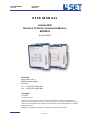
SET9010MAN0001 Issue: 01 USER MANUAL RDK9314 USER MANUAL COMPACTRIO RESOLVER TO DIGITAL CONVERSION MODULE RDK9314 Art.Nr. 85019 SET GmbH August-Braun-Str. 1 88239 Wangen/Allgäu Germany Tel.: +49 (0)7522 91687-600 Fax: +49 (0)7522 91687-899 Copyrights: SET GmbH All rights reserved. Information contained herein is the property of SET GmbH and shall not be duplicated, copied, used or disclosed in whole or in part of any purpose. The right of duplication, use or disclosure is permitted only by written agreement of SET GmbH, August Braun Str. 1, 88239 Wangen/Germany. LabVIEW, CompactRIO, TestStand are Trademarks of National Instruments Page 1 of 35 SET9010MAN0001 Issue: 01 USER MANUAL RDK9314 TABLE OF CONTENTS 1. Important Instructions ....................................................................................................................... 4 1.1 Initial Inspection ................................................................................................................................. 4 1.2 Safety Instructions .............................................................................................................................. 4 1.2.1 Module Failure ................................................................................................................................... 4 1.2.2 Impermissible Applications ................................................................................................................ 4 1.2.3 Module Installation And Removal ...................................................................................................... 4 1.2.4 Electrical Connections ........................................................................................................................ 4 2. Module Overview ............................................................................................................................... 5 3. Getting Started ................................................................................................................................... 6 3.1 Software-Installation .......................................................................................................................... 6 3.2 RDK9314 CompactRIO LabVIEW Drivers ............................................................................................. 7 3.2.1 Create New Projects By Use Of The Example Project .......................................................................... 8 3.2.2 Driver Application For A NI PCI-FPGA-Card ....................................................................................... 10 3.2.2.1 Creating A New Project..................................................................................................................... 10 3.2.2.2 Creating A New FPGA-Target (NI FPGA PCI/PXI- Card) ...................................................................... 11 3.2.2.3 Adding An R-Series Expansion Chassis .............................................................................................. 13 3.2.2.4 Adding The RDK9314 Hardware Components To A Project ............................................................... 14 3.2.2.5 Adding The Driver Software Components ......................................................................................... 15 3.2.2.6 Adding The FPGA Application Example ............................................................................................. 16 3.2.2.7 Saving The New Project .................................................................................................................... 18 3.2.2.8 Compilation And Example Execution ................................................................................................ 18 3.3 Connecting The Resolver .................................................................................................................. 20 3.4 Running The Application................................................................................................................... 20 3.5 Operating Details.............................................................................................................................. 21 3.5.1 Driver Call And Data Transfer ........................................................................................................... 21 3.5.1.1 FIFO-Data Transfer ........................................................................................................................... 21 3.5.1.2 Data Frame Setup ............................................................................................................................. 21 3.5.1.3 Embedding And Calling The RDK9314 FPGA-Driver ........................................................................... 23 3.5.2 Commands ....................................................................................................................................... 25 3.6 Module Identification Under LabVIEW ............................................................................................. 29 3.7 Saving The Setup .............................................................................................................................. 29 3.8 Auto Ratio ........................................................................................................................................ 29 4. Software Development..................................................................................................................... 30 4.1 Example 1: Manually Triggered Position Measurement (Direct Mode) ............................................ 30 Page 2 of 35 SET9010MAN0001 Issue: 01 USER MANUAL RDK9314 4.2 Example 2: Manually Triggered Position Measurement (Indirect Mode) ......................................... 30 4.3 Example 3: Continuous Position Measurement ............................................................................... 31 5. Technical Specification ..................................................................................................................... 32 5.1 Housing ............................................................................................................................................ 32 5.2 External Power Supply...................................................................................................................... 32 5.3 Excitation Ouput............................................................................................................................... 32 5.4 Sinus And Cosinus Signal Inputs........................................................................................................ 32 5.5 Position Processing ........................................................................................................................... 33 5.6 Environmental Conditions ................................................................................................................ 33 5.7 Connector Pinout.............................................................................................................................. 33 6. Module Calibration ........................................................................................................................... 34 6.1 Calibration Of The Excitation Voltage Amplitude .............................................................................. 34 6.2 Calibration Of The Input Channels .................................................................................................... 34 7. Module Maintenance ....................................................................................................................... 35 8. Service Address ................................................................................................................................ 35 Page 3 of 35 SET9010MAN0001 Issue: 01 1. USER MANUAL RDK9314 IMPORTANT INSTRUCTIONS Please read all instructions carefully before the RDK9314 is installed into a cRIO chassis or connected to other equipment! 1.1 INITIAL INSPECTION Check that the shipment is complete and note whether any damage has occurred during transport. If the contents are incomplete or there is damage, file a claim with the carrier immediately, and notify the SET GmbH service contact to facilitate the repair or replacement of the module. The address is listed in the back of the manual. The following parts should be included in the shipment: RDK9314 module CD-ROM with driver software and application examples User manual 1.2 SAFETY INSTRUCTIONS 1.2.1 MODULE FAILURE Do not install the RDK9314 module into a cRIO chassis when the module is obviously damaged: • • • physical damage lose parts inside the module it does not function any more 1.2.2 IMPERMISSIBLE APPLICATIONS The module is designed for laboratory use. Installing or operating the module in explosive or hazardous environments is not permissible and may result in serious injury or death! 1.2.3 MODULE INSTALLATION AND REMOVAL Hot Surface! The module may be hot. Touching the module may result in body injury 1.2.4 ELECTRICAL CONNECTIONS The module is not designed to isolate voltage levels of more than 50VDC. Do not exceed the voltage levels according to the technical specifications. Not following this instruction may result in module damage and serious injury or death! Page 4 of 35 SET9010MAN0001 Issue: 01 2. USER MANUAL RDK9314 MODULE OVERVIEW Sensor Controll demod. freq. RDK 9314 is a compact, reliable and highly versatile Resolver-to-digital conversion module. All commonly used Resolvers can be easily connected to the module without any additional signal adaption. The module has a built-in excitation oscillator inclusive power stage which can drive most Resolvers directly without the necessity of an external power booster. All module parameter are interactively adjustable via software. A sensor-detection functionality automatically adjusts the module to the specific sensor ratio. RDK 9314 The RDK 9314 accepts a wide voltage supply range from 18V to 36V and provides galvanic isolation between the cRIO rack and the demodulator interface. The module is operable within the NI cRIO real time environment and can also be plugged into a NI R-series expansion chassis with PCI / PXI FPGA card. Included in delivery are all drivers required for the cRIO systems and LabVIEW/TestStand integration examples. Resolver Engine 18-36V Reg Demodulator Excitation VSUP + COM SIN HI SIN LO COS HI COS LO EXEC HI EXEC LO RDK9314 applications include industrial and military position control systems such as motor control, robotics and many kind of servo loops which use Resolvers. Page 5 of 35 SET9010MAN0001 Issue: 01 USER MANUAL RDK9314 3. GETTING STARTED 3.1 SOFTWARE-INSTALLATION Before the RDK9314 module may be used in a LabVIEW project the driver software must be installed. To do this use the RDK9314 CD-ROM and follow the following instructions. To start the installation process, execute the „setup.exe” program on the CD-ROM. Click the start button to confirm the software installation. When the installation is completed successfully, the following message appears: The host system is now ready for use the RDK314 module in a LabVIEW project. Page 6 of 35 SET9010MAN0001 Issue: 01 3.2 USER MANUAL RDK9314 RDK9314 COMPACTRIO LABVIEW DRIVERS To use of the CompactRIO RDK9314 driver software LabVIEW 8.6. must be installed. The driver software includes a FPGA diver-VI which installs the required FIFO registers to communicate with the application software. Note that the FPGA applies SPI interfaces to exchange data with the RDK9314 module. RDK9314 FPGA driver-VI (for Slot 1) Depending on the type of chassis (R-Series Expansion- or Real Time CompactRIO – chassis) up to eight RDK9314 modules can be operated in parallel within one chassis. Every module within a chassis applies separate data lines and hence every module requires a separate driver-VI. Each slot applies a separate driver-VI Three example applications can be found on the CD-ROM to demonstrate the structure and operation of the driver-VI’s: • FPGA APPLICATION EXAMPLE (Slot 1).vi This is an application example which demonstrates the use of one single RDK9314 module which is installed in slot 1 of a (PCI) FPGA R-Series Expansion-Chassis or a cRIO-Realtime chassis. • FPGA APPLICATION EXAMPLE MULTIPLE (PCI - 4 Slots).vi This is an application example which demonstrates the parallel operation of up to four RDK9314 modules in a (PCI) FPGA R-Series Expansion-Chassis. • FPGA APPLICATION EXAMPLE MULTIPLE (RT cRIO - 8 Slots).vi This is an application example which demonstrates the parallel operation of up to eight RDK9314 modules in a cRIO-Realtime-Chassis. The following chapters explain the implementation of the driver files into a new LabVIEW project. Example VI „FPGA APPLICATION EXAMPLE (Slot 1).vi“ is applicable for both, a PCIFPGA Target with R-Series Expansion Chassis and the cRIO Realtime Platform. Page 7 of 35 SET9010MAN0001 Issue: 01 USER MANUAL RDK9314 3.2.1 CREATE NEW PROJECTS BY USE OF THE EXAMPLE PROJECT The example project helps to create a new project. To create a new project, simply transfer the required driver modules via drag-and-drop into the new project. Relates to an internal NI PCIFPGA-Card in combination with a (4 Slot) R-Series Expansion Chassis Relates to an RealTime CompactRIO FPGATarget Additionally, a small FPGA application (which uses slot 1), is on the CD-ROM to demonstrate the call and use of the RDK9314 driver: Page 8 of 35 SET9010MAN0001 Issue: 01 USER MANUAL RDK9314 To use the RDK9314 driver within an existing LabVIEW project, copy all files from the example project folder into the existing project folder: Page 9 of 35 SET9010MAN0001 Issue: 01 USER MANUAL RDK9314 3.2.2 DRIVER APPLICATION FOR A NI PCI-FPGA-CARD 3.2.2.1 CREATING A NEW PROJECT In order to use the RDK9314 driver for a new project, first open the example project and then select „File New Project“. Page 10 of 35 SET9010MAN0001 Issue: 01 USER MANUAL RDK9314 3.2.2.2 CREATING A NEW FPGA-TARGET (NI FPGA PCI/PXI- CARD) Both project windows can be aligned as shown below: To add a new FPGA-Target use the mouse and click (right button) onto the computer symbol and select: „New Targets and Devices“. Page 11 of 35 SET9010MAN0001 Issue: 01 USER MANUAL RDK9314 Select an existing FPGA-Target or define a new device. The new FGPA-Target is now added to the project-structure. Page 12 of 35 SET9010MAN0001 Issue: 01 USER MANUAL RDK9314 3.2.2.3 ADDING AN R-SERIES EXPANSION CHASSIS To use an RDK9314 module together with a FPGA chassis, an „R-Series Expansion Chassis“ must be appended to the actual project structure. Use the mouse and click with the right button onto the newly added FPGA-Target and select „New R Series Expansion Chassis“. Confirm the dialog with „OK“. Page 13 of 35 SET9010MAN0001 Issue: 01 USER MANUAL RDK9314 The newly added R-Series Expansion Chassis is now included in the project structure: 3.2.2.4 ADDING THE RDK9314 HARDWARE COMPONENTS TO A PROJECT To add a specific cRIO module to the FPGA chassis use the drag-and-drop function to copy the file from the example project into the new project. Note that the STRG-key must be pressed during drag-and-drop to copy the element. Otherwise the element will be removed from the example project. This operation automatically installs the I/O-channels of the module within a new folder as shown below: Page 14 of 35 SET9010MAN0001 Issue: 01 USER MANUAL RDK9314 3.2.2.5 ADDING THE DRIVER SOFTWARE COMPONENTS Every module of the example projects uses a separate folder which includes the driver-VI and three different FIFO buffers. These sub-folders must also be copied into the new project for every new module import. To do this, drag the applicable sub-folder into the new project structure while the STRG-key is pressed. All relevant driver files are now added to the new project: Page 15 of 35 SET9010MAN0001 Issue: 01 USER MANUAL RDK9314 3.2.2.6 ADDING THE FPGA APPLICATION EXAMPLE A small example application on the CD-ROM demonstrates the driver usage. This example explains how the driver is used for an RDK9314 module installation on slot 1. Use the drag-and-drop function to copy the example into the new project structure. Please note that the STRG-key must be pressed to copy the elements rather than moving them. Page 16 of 35 SET9010MAN0001 Issue: 01 USER MANUAL RDK9314 The copied example application can now be found in the new project structure as shown below: Page 17 of 35 SET9010MAN0001 Issue: 01 USER MANUAL RDK9314 3.2.2.7 SAVING THE NEW PROJECT Prior to the compilation process the project must be saved. To do this, click on “File Save All”. Enter a file name for new projects. 3.2.2.8 COMPILATION AND EXAMPLE EXECUTION Open VI „FPGA APPLICATION EXAMPLE (Slot 1).vi“ out of the project structure and click the “Run” button. The compilation process starts now and may take up to 25 minutes processing time. Note that the compilation time increases with the number of modules in the application because every module requires a separate driver-VI and a separate FIFO buffers. Page 18 of 35 SET9010MAN0001 Issue: 01 USER MANUAL RDK9314 The following window is shown when the compiling process is complete: Note: The same principle applies for the NI RealTime CompactRIO platform. An example on the CDROM illustrates this application. Page 19 of 35 SET9010MAN0001 Issue: 01 3.3 USER MANUAL RDK9314 CONNECTING THE RESOLVER To make the RDK9314 ready for use plug the module into the correct slot of the cRIO Chassis. Make sure, to select the correct slot according to the LabVIEW project definition. Then connect the modules external power supply (18VDC – 36VDC) as shown below. Do not turn on power before the Resolver connection is accomplished. Connect the Resolver interface as shown below (see also paragraph Fehler! Verweisquelle konnte nicht gefunden werden.). When all connection is complete, the external power supply can be switched on. Note that the RDK9314 module will not be detected from the chassis before the modules external power supply is switched on. 3.4 RUNNING THE APPLICATION Make sure that: Application compiling process is complete The module is plugged into the correct slot according to the application The Resolver and the external supply is connected The external power supply is switched on The cRIO Chassis supply is switched on The LabVIEW-VI can now be started by clicking the “Run”-button. Use parameters Amplitude [mV] and Frequency [Hz] to adjust the excitation signal to the correct level. For a precise demodulation process the RDK9314 must be adapted to the signal transfer ratio of the Resolver. This is accomplished by executing the function Auto Ratio which automatically adjusts the RDK9314 module to the Resolver transfer ratio. Note that the Resolver must be connected to the module for this process. When the Resolver type is changed, make sure to execute Auto Ratio again. Page 20 of 35 SET9010MAN0001 Issue: 01 3.5 USER MANUAL RDK9314 OPERATING DETAILS 3.5.1 DRIVER CALL AND DATA TRANSFER 3.5.1.1 FIFO-DATA TRANSFER FPGA FIFO buffers are used to transfer data between the calling application and the driverVI’s. In total, three FPGA FIFO buffers exist for each module slot: Send commands and data Receive data (and command) Busy-Status of the module • COMMANDIN-FIFO: This buffer transfers instructions and data to the RDK3914 module driver. The buffer size is 20 elements (U32) and can be expanded as necessary. • COMMANDOUT-FIFO: This buffer receives data and the echoed instruction from the RDK3914 module driver. The buffer size is 20 elements (U32) and can be expanded as necessary. • MODULEBUSY -FIFO: This buffer continuously indicates the RDK9314 busy state. The ModuleBusy-Flag (Boolean) is active when the RDK9314 controller is processing data. The buffer size is 20 elements (U32) and can be expanded as necessary. 3.5.1.2 DATA FRAME SETUP TRANSMITTING DATA TO THE RDK9314 MODULE: To send data to the module driver a U32-Integer (4 byte) data format applies. The data simply must be written into the CommandIn-FIFO buffer. Command [U8] [U16] Not used [U8] Data [U16] FIFO-DATA [U32] Slot N CommandIn-FIFO [U16] Slot N Driver-VI Slot N RDK-Module • COMMAND [U8] This is the command to the RDK9314. See paragraph 3.5.2 for the command list. • DATA [U16]: Data format is U16. See paragraph 3.5.2 for more details. Page 21 of 35 SET9010MAN0001 Issue: 01 USER MANUAL RDK9314 RECEIVING DATA FROM THE RDK9314 MODULE: Receiving data from the module driver are buffered in the applicable CommandOut-FIFO. The data format is U32-Integer (4 Byte). Command [U8] FIFO-DATA [U32] Slot N RDK-Module Slot N Driver-VI Slot N CommandOut-FIFO [U16] [U16] Error-Code [U8] Data [U16] • COMMAND [U8]: Echoes the last received command with one exception: the NOP command will not be echoed. See also paragraph 3.5.2 for more details. • ERROR [U8]: Includes the error code which is generated from the module. See also paragraph 3.5.2 for more details. • DATA [U16]: The format of the received data is U16. See also paragraph 3.5.2 for more details. Page 22 of 35 SET9010MAN0001 Issue: 01 USER MANUAL RDK9314 3.5.1.3 EMBEDDING AND CALLING THE RDK9314 FPGA-DRIVER EMBEDDING THE DRIVER FOR ONE SINGLE MODULE: The following drawing illustrates the RDK9314 driver call (one single module) out of the FPGA application environment. Note that the FPGA driver runs in parallel outside the rest of the program code. Refer to the example on the CD-ROM. Service Call of a Single Driver-Vis (Example Module 1 / Slot 1) Page 23 of 35 SET9010MAN0001 Issue: 01 USER MANUAL RDK9314 EMBEDDING THE DRIVER FOR MORE THAN ONE MODULE: To operate multiple modules the specific driver-VI’s are all operated strictly parallel to the other program code. All communication between the application program and the driverVI’s takes place via the module specific FIFO buffers. Service Call for Multiple Driver-VI’s Page 24 of 35 SET9010MAN0001 Issue: 01 USER MANUAL RDK9314 3.5.2 COMMANDS All module commands are defined in TypeDef „RDKCMD.ctl“. COMMAND: VALUE [U8]: TARGET: CMD_NOP 0 RDK9314 Controller This instruction sends a NOP-command to the RDK9314 controller and is used internally for the driver communication to cope with the SPI communication principles. COMMAND: VALUE [U8]: TARGET: CMD_RD_POS 1 RDK9314 Controller This instruction (DATA = 0) reads the actual position of the Resolver. The read value (16 bit) is raw data and maps the Resolver angle from 0° to 360° to the integer data range of 0 to 65535. Note that this data range is used for both, the 14-bit and the 16bit mode. To calculate the Resolver angle in °[DEG] use the following equation: ϕ DEG = DATA ⋅ 360 65536 COMMAND: VALUE [U8]: TARGET: CMD_RD_AMP 3 RDK9314 Controller This instruction (DATA = 0) reads back the commanded excitation voltage level. The voltage level data format is 16 bit integer with 1 lsb equal to 1[mVRMS]. COMMAND: VALUE [U8]: TARGET: CMD_RD_FRQ 4 RDK9314 Controller This instruction (DATA = 0) reads back the commanded excitation voltage frequency. The frequency data format is 16 bit integer with 1 lsb equal to 1[Hz]. COMMAND: VALUE [U8]: TARGET: CMD_RD_RAT 5 RDK9314 Controller This instruction reads back the adjusted transfer ratio. The data format is 16 bit integer and mapped as follows: 0 for Ratio = 0.0 1000 for Ratio = 1.0 Page 25 of 35 SET9010MAN0001 Issue: 01 USER MANUAL RDK9314 COMMAND: VALUE [U8]: TARGET: CMD_RD_SIN_VOL 6 RDK9314 Controller This instruction (DATA = 0) reads the voltage of the sine input channel. The voltage data format is 16 bit integer with 1 lsb equal to 1[mVRMS]. Note that for calculating the Usin[VRMS] voltage requires a processing time of 25μs, this operation allows a maximum sampling rate of 40kHz. COMMAND: VALUE [U8]: TARGET: CMD_RD_COS_VOL 7 RDK9314 Controller This instruction (DATA = 0) reads the voltage of the cosine input channel. The voltage data format is 16 bit integer with 1 lsb equal to 1[mVRMS]. Note that for calculating the Ucos[VRMS] voltage requires a processing time of 25μs, this operation allows a maximum sampling rate of 40kHz. COMMAND: VALUE [U8]: TARGET: CMD_WR_RES_MODE 8 RDK9314 Controller This instruction adjusts the angular resolution of the RDK9314 module to 12/14 or 16-Bit. DATA = 0 DATA = 1 DATA = 2 High Resolution Normal Resolution Low Resolution (16-Bit) (14-Bit) (12-Bit) COMMAND: VALUE [U8]: TARGET: CMD_WR_AMP 9 RDK9314 Controller This instruction adjusts the modules excitation voltage. The voltage data format is 16 bit integer with 1 lsb equal to 1[mVRMS]. COMMAND: VALUE [U8]: TARGET: CMD_WR_FRQ 10 RDK9314 Controller This instruction adjusts the modules excitation frequency. The frequency data format is 16 bit integer with 1 lsb equal to 1[Hz]. COMMAND: VALUE [U8]: TARGET: CMD_WR_RAT 11 RDK9314 Controller This instruction manually adjusts the Resolver transfer ratio which is useful to copy ratio data from other modules. Page 26 of 35 SET9010MAN0001 Issue: 01 USER MANUAL RDK9314 The data format is 16 bit integer and mapped as follows: 0 for Ratio = 0.0 1000 for Ratio = 1.0 COMMAND: VALUE [U8]: TARGET: CMD_CAL_EXC 12 RDK9314 Controller This instruction calibrates the excitation voltage level. To calibrate the output voltage level refer to paragraph 5.1. COMMAND: VALUE [U8]: TARGET: CMD_AUTO_CAL 13 RDK9314 Controller This instruction (DATA = 0) initializes an automatic calibration procedure for the modules input channels. Refer to paragraph 5 more details. COMMAND: VALUE [U8]: TARGET: CMD_AUTO_RAT 14 RDK9314 Controller This instruction (DATA = 0) initializes a procedure which adjusts the RDK3914 to the transfer ratio of the connected Resolver. Note that this instruction must be processed when the Resolver type is changed or a Resolver is connected to the module the first time. COMMAND: VALUE [U8]: TARGET: CMD_IDLE_OPERATION 15 FPGA Driver-VI The driver VI’s offer a specific operational mode which sends instructions to the RDK3914 in a cyclical manner. This, for instance, is helpful to monitor a Resolver position permanently. In this case the position data is permanently buffered in the CommandOut-FIFO. Thus, the sampling speed increases as no polling mechanism is required any more. In this automatic mode, the module cyclically processes the “idle” function (which is actually not idling) when no other instruction is received. When the module operates the automatic mode and receives an instruction, then the automatic sampling is interrupted for the processing time which is required to operate this instruction. The automatic mode can be programmed as follows: • NOP 0 Deactivate the Idle-Command • CMD_RD_POS 1 Read Resolver Position • CMD_RD_AMP 3 Read Excitation Amplitude • CMD_RD_FRQ 4 Read Excitation Frequency • CMD_RD_RAT 5 Read Resolver Ratio • CMD_RD_SIN_VOL 6 Read Resolver Sine-Voltage [VRMS] • CMD_RD_COS_VOL 7 Read Resolver Cosine-Voltage [VRMS] Page 27 of 35 SET9010MAN0001 Issue: 01 USER MANUAL RDK9314 Refer to the TypeDef „USRCMD.ctl“ for these instructions. COMMAND: VALUE [U8]: TARGET: CMD_CYCLE_SPEED 16 FPGA Driver-VI This instruction adjusts the idle-frequency for (CMD_IDLE_OPERATION). The standard value is 50kHz. the automatic mode Note: Changing the cycle speed has an influence on the latency time of the manual mode operation. Furthermore, if Usin/cos[VRMS]values are sampled by use of the automatic mode, the sampling speed must not exceed 40kHz to get correct voltage readings. To ensure correct operation for automatic rms readings, first the cycle time with “CMD_CYCLE_SPEED” must be programmed to a value < 40kHz. This restriction applies only to Usin/cos[VRMS]voltage readings but not to the Resolver position readings, which allow 50kHz sampling rate for both operational modes. COMMAND: VALUE [U8]: TARGET: CMD_RESET 17 RDK9314 Controller This instruction (DATA = 0) resets the RDK9314 internal controller chip. COMMAND: VALUE [U8]: TARGET: CMD_STOP 18 FPGA Driver-VI This instruction stops and terminates the applicable driver-VI. Page 28 of 35 SET9010MAN0001 Issue: 01 3.6 USER MANUAL RDK9314 MODULE IDENTIFICATION UNDER LABVIEW LabVIEW automatically detects the cRIO module type (Discover C-Series Modules). Note that the external module supply must be connected for the automatic RDK9314 identification. 3.7 SAVING THE SETUP The RDK9314 automatically saves the setup in a non-volatile memory. 3.8 AUTO RATIO The Auto Ratio function (CMD_AUTO_RAT) automatically adjusts the RDK9314 to the transfer ratio of the connected Resolver. The Auto Ratio must be triggered when the type of Resolver is changed or a Resolver is connected to the module for the first time. Note that position readings may be incorrect or out of tolerance when the module is not adjusted to the Resolver transfer ratio. Page 29 of 35 SET9010MAN0001 Issue: 01 4. USER MANUAL RDK9314 SOFTWARE DEVELOPMENT The example driver software addresses all module features and thus requires a reasonable amount of the FPGA resources. However, not all features must be used in order to save FPGA resources and to speed up the compilation process. This is demonstrated in the following applications. 4.1 EXAMPLE 1: MANUALLY TRIGGERED POSITION MEASUREMENT (DIRECT MODE) 4.2 EXAMPLE 2: MANUALLY TRIGGERED POSITION MEASUREMENT (INDIRECT MODE) This example applies a “Read Position” button which triggers the CMD_RD_POS instruction. The “Stop” button sends the instruction CMD_STOP to the driver and terminates the program. A parallel program loop extracts the position data from the FIFO and copies the data to the visualization element. Additionally, a second parallel program loop checks the modules busy state. This is compulsory because every FIFO which is imported from the driver-VI must be read at least one time. Page 30 of 35 SET9010MAN0001 Issue: 01 4.3 EXAMPLE 3: USER MANUAL RDK9314 CONTINUOUS POSITION MEASUREMENT This example configures the RDK9314 driver for continuous measurement. A software loop cyclically reads the position data from the module. When the “Stop” button is clicked, the CMD_STOP instruction is sent to the module which terminates the program. Furthermore, another parallel software loop reads the modules busy state as already explained in the examples before. Page 31 of 35 SET9010MAN0001 Issue: 01 USER MANUAL RDK9314 5. TECHNICAL SPECIFICATION 5.1 HOUSING • NI CompactRIO 9952 Standard Housing • Dimensions: appr. 71mm x 72mm x 23mm 5.2 EXTERNAL POWER SUPPLY • Supply Voltage: • Current Consumption: 18VDC – 36VDC max. 50mA at 28VDC without Resolver Caution: The external power supply input is isolated from the cRIO chassis signals with a maximum isolation voltage of 50Vdc. Note that the excitation output and the Sine/Cosine input signals are galvanically connected to the external power supply. 5.3 EXCITATION OUPUT • Frequency: • Amplitude: • Current: 1kHz – 10kHz, adjustable via software 2VRMS – 7 VRMS, adjustable via software max. 150mARMS, short cct protected Caution: The excitation output can be damaged when a power source is connected to its terminals. 5.4 SINUS AND COSINUS SIGNAL INPUTS • Voltage Range: • Zin (differential): 2VRMS – 7 VRMS 54kOhm Page 32 of 35 SET9010MAN0001 Issue: 01 USER MANUAL RDK9314 • Zin (single-ended): 27kOhm Caution: The signal inputs can be damaged, when the input voltage exceeds a limit of 40V peak. 5.5 POSITION PROCESSING • • • • • 5.6 Resolution: Accuracy: Acceleration: Settling Time (179°-step): Tracking Rate (min): ENVIRONMENTAL CONDITIONS • Temperature Range: • Humidity: 5.7 12/14/16Bit, adjustable via software 2.3/3.3 Arc min (at 1 – 4kHz / 4 – 10kHz) 500kdeg/s² (12Bit) / 30kdeg/s² (14Bit) / 2kdeg/s² (16Bit) 8msec (12Bit) / 20msec (14Bit) / 50msec (16Bit) 432rps (12Bit) / 108rps (14Bit) / 27rps (16Bit) 0°C – 70°C 10% – 90% relative, non-condensing CONNECTOR PINOUT User Interface Connector (25-pin dSUB / male): Pin Function 1 VSUP 2 COM 3 GND 4 +SIN 5 -SIN 6 GND 7 +COS 8 -COS 9 GND 10 +EXC 11 -EXC 12 - 25 n.c. Page 33 of 35 SET9010MAN0001 Issue: 01 6. USER MANUAL RDK9314 MODULE CALIBRATION The RDK9314 is calibrated when shipped. If a periodical calibration is compulsory due to the field of application, the module can be re-calibrated from the supplier or by the user. To do this the following procedure must be followed: 6.1 CALIBRATION OF THE EXCITATION VOLTAGE AMPLITUDE • Plug the RDK9314 into slot 1 of a cRIO chassis and connect the external supply voltage to the module. • Open example VI „FPGA APPLICATION EXAMPLE (Slot1).vi“ out of the project structure and click on the button “Run”. • Program the excitation amplitude to 7000[mVRMS] and the frequency to 10kHz. • Connect a true RMS volt meter to the excitation output signal. The voltage meter must ensure a 0.05% accuracy for the 7.000[VRMS] measurement range (10kHz sinusoidal waveform). • Adjust an ExcitationCalData value of “3290” with the CMD_CAL_EXC instruction and check the excitation output voltage. • Iteratively reprogram the ExcitationCalData stepwise until the excitation output voltage reading is 7.000[VRMS]. To increase the output voltage, increase the ExcitationCalData. To decrease the output voltage, decrease the ExcitationCalData. The ExcitationCalData can be programmed within the range of [3260 – 3420]. 6.2 CALIBRATION OF THE INPUT CHANNELS • Connect the module interface as shown below. Note that procedure 6.1 must be accomplished before the input channels can be calibrated. • Execute instruction CMD_AUTO_CAL. On completion of this instruction, the module calibration is complete and the calibration data is saved in the non-volatile module memory. Page 34 of 35 SET9010MAN0001 Issue: 01 USER MANUAL RDK9314 7. MODULE MAINTENANCE No maintenance is required for the RDK9314 module. 8. SERVICE ADDRESS For technical support contact the SET service address: SET GmbH August-Braun-Str. 1 88239 Wangen/Allgäu Germany Tel.: +49 (0)7522 91687-600 Fax: +49 (0)7522 91687-899 e-Mail: [email protected] Page 35 of 35