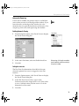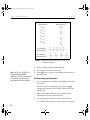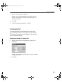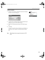
1
Scug.bk Page 1 Monday, September 13, 1999 12:57 PM
PSpice Schematics
Schematic Capture Software
User’s Guide
Scug.bk Page 2 Monday, September 13, 1999 12:57 PM
Release 9.1, November, 1999.
Copyright 1999 OrCAD, Inc. All rights reserved.
TradeMarks
Referenced herein are the trademarks used by OrCAD, Inc. to identify its products. OrCAD Corporation
is the exclusive owner of “OrCAD,” “PSpice,” “PLogic,” “PLSyn.”
Additional marks of OrCAD include: “StmEd,” “Stimulus Editor,” “Probe,” “Parts,” “Monte Carlo,”
“Analog Behavioral Modeling,” “Device Equations,” “Digital Simulation,” “Digital Files,” “Filter
Designer,” “Schematics,” “PLogic,” “PSpice Optimizer,” and “PLSyn” and variations theron (collectively
the “Trademarks”) are used in connection with computer programs. OrCAD owns various trademark
registrations for these marks in the United States and other countries.
Microsoft, MS-DOS, Windows, Windows NT and the Windows logo are either registered trademarks or
trademarks of Microsoft Corporation.
Adobe, the Adobe logo, Acrobat, the Acrobat logo, Exchange and PostScript are trademarks of Adobe
Systems Incorporated or its subsidiaries and may be registered in certain jurisdictions.
EENET is a trademark of Eckert Enterprises.
All other company/product names are trademarks/registered trademarks of their respective holders.
Copyright Notice
Except as permitted under the United States Copyright Act of 1976, no part of this publication may be
reproduced or distributed in any form or by any means, or stored in a data base or retrieval system,
without the prior written permission of OrCAD, Inc.
As described in the license agreement, you are permitted to run one copy of the OrCAD software on one
computer at a time. Unauthorized duplication of the software or documentation is prohibited by law.
Corporate Program Licensing and multiple copy discounts are available.
Technical Support
Internet
[email protected]
Phone
FAX
WWW
(503) 671-9400
(503) 671-9501
http://www.orcad.com
Sales
Phone
(800) 671-9505
9300 SW Nimbus Ave.
Beaverton, OR 97008 USA
Scug.bk Page iii Monday, September 13, 1999 12:57 PM
Contents
Before You Begin
xv
Welcome to OrCAD . . . . . . .
PSpice Schematics Overview . .
How to Use this Guide . . . . .
Typographical Conventions
Related Documentation . . . . .
Online Help . . . . . . . . .
Chapter 1
Chapter 2
.
.
.
.
.
.
.
.
.
.
.
.
.
.
.
.
.
.
.
.
.
.
.
.
.
.
.
.
.
.
.
.
.
.
.
.
.
.
.
.
.
.
.
.
.
.
.
.
.
.
.
.
.
.
.
.
.
.
.
.
. . xv
. xvi
xviii
xviii
. xix
. . xx
Overview . . . . . . . . . . . . . . . . . . . . . . . . . .
Using PSpice Schematics . . . . . . . . . . . . . . . . .
Example—Drawing a Schematic . . . . . . . . . . . . .
Starting a New Design . . . . . . . . . . . . . . . .
Command Line Options . . . . . . . . . . . . . . .
Checking Symbol Libraries Configuration . . . . .
Selecting and Placing Parts . . . . . . . . . . . . . .
Drawing and Labeling Wires . . . . . . . . . . . .
Drawing and Labeling Buses . . . . . . . . . . . . .
Changing Reference Designators and Part Values .
Moving Parts, Wires, and Text . . . . . . . . . . . .
Placing Ports . . . . . . . . . . . . . . . . . . . . . .
Placing Power and Ground Symbols . . . . . . . .
Saving Your Work . . . . . . . . . . . . . . . . . . .
.
.
.
.
.
.
.
.
.
.
.
.
.
.
.
.
.
.
.
.
.
.
.
.
.
.
.
.
.
.
.
.
.
.
.
.
.
.
.
.
.
.
.
.
.
.
.
.
.
.
.
.
.
.
.
.
.
.
.
.
.
.
.
.
.
.
.
.
.
.
.
.
.
.
.
.
.
.
.
.
.
.
.
.
.
.
.
.
.
.
.
.
.
.
.
.
.
.
.
.
.
.
.
.
.
.
.
.
.
.
.
.
.
.
.
.
.
.
.
.
.
.
.
.
.
.
.
.
.
.
.
.
.
.
.
.
.
.
.
.
.
.
.
.
.
.
.
.
.
.
.
.
.
.
1
2
4
6
6
7
8
11
12
14
15
16
17
18
.
.
.
.
.
.
.
.
.
.
.
.
.
.
.
.
.
.
.
.
.
.
.
.
.
.
.
.
.
.
.
.
.
.
.
.
.
.
.
.
.
.
.
.
.
.
.
.
.
.
.
.
.
.
.
.
.
.
.
.
.
.
.
.
.
.
19
20
22
23
25
25
Getting Started
.
.
.
.
.
.
.
.
.
.
.
.
.
.
.
.
.
.
.
.
.
.
.
.
.
.
.
.
.
.
.
.
.
.
.
.
.
.
.
.
.
.
.
.
.
.
.
.
.
.
.
.
.
.
.
.
.
.
.
.
.
.
.
.
.
.
.
.
.
.
.
.
1
Using Design Manager
19
Overview . . . . . . . . . . . . . . . . .
Understanding Design Manager . . . .
Managing Your Files in the Workspace
Design Manager Functions . . . . . . .
Starting the Design Manager . . . . . .
Hints and Tips . . . . . . . . . . . . . .
.
.
.
.
.
.
.
.
.
.
.
.
.
.
.
.
.
.
.
.
.
.
.
.
.
.
.
.
.
.
.
.
.
.
.
.
.
.
.
.
.
.
.
.
.
.
.
.
.
.
.
.
.
.
Scug.bk Page iv Monday, September 13, 1999 12:57 PM
Contents
September 13, 1999
Design Manager Help . . . . . . . . . . . . . . . . . . . . . . . . . . . . . 25
Chapter 3
Using the Schematic Editor
27
Overview . . . . . . . . . . . . . . . . . . . . .
Components of a Design . . . . . . . . . . . . .
Parts . . . . . . . . . . . . . . . . . . . . . .
Symbols . . . . . . . . . . . . . . . . . . . .
Ports . . . . . . . . . . . . . . . . . . . . . .
Attributes . . . . . . . . . . . . . . . . . . .
Annotations . . . . . . . . . . . . . . . . . .
Connections . . . . . . . . . . . . . . . . . .
Main Window . . . . . . . . . . . . . . . . . .
Menus . . . . . . . . . . . . . . . . . . . . .
Toolbars . . . . . . . . . . . . . . . . . . .
Status Bar . . . . . . . . . . . . . . . . . . .
Refreshing the Screen . . . . . . . . . . . .
Keyboard . . . . . . . . . . . . . . . . . . .
Configuring PSpice Schematics . . . . . . . . .
Configuring Symbol Libraries . . . . . . .
Changing Page Size . . . . . . . . . . . . .
Changing Page Settings . . . . . . . . . . .
Changing Grid and Gravity . . . . . . . . .
Setting the Autosave Interval . . . . . . . .
Controlling the Display in PSpice Schematics .
Changing Fonts . . . . . . . . . . . . . . .
Configuring Colors . . . . . . . . . . . . .
Changing Application Settings . . . . . . .
Changing the Get Recent Part List Size . .
Zooming and Panning in PSpice Schematics .
Zooming . . . . . . . . . . . . . . . . . . .
Setting Zoom Parameters . . . . . . . . . .
Fitting to a Page . . . . . . . . . . . . . . .
Panning . . . . . . . . . . . . . . . . . . . .
Using the Message Viewer . . . . . . . . . . .
Online Help . . . . . . . . . . . . . . . . . .
Locating the Source of a Message . . . . .
Indicated Severity . . . . . . . . . . . . . .
Additional Information . . . . . . . . . . .
Closing the Message Viewer . . . . . . . .
iv
.
.
.
.
.
.
.
.
.
.
.
.
.
.
.
.
.
.
.
.
.
.
.
.
.
.
.
.
.
.
.
.
.
.
.
.
.
.
.
.
.
.
.
.
.
.
.
.
.
.
.
.
.
.
.
.
.
.
.
.
.
.
.
.
.
.
.
.
.
.
.
.
.
.
.
.
.
.
.
.
.
.
.
.
.
.
.
.
.
.
.
.
.
.
.
.
.
.
.
.
.
.
.
.
.
.
.
.
.
.
.
.
.
.
.
.
.
.
.
.
.
.
.
.
.
.
.
.
.
.
.
.
.
.
.
.
.
.
.
.
.
.
.
.
.
.
.
.
.
.
.
.
.
.
.
.
.
.
.
.
.
.
.
.
.
.
.
.
.
.
.
.
.
.
.
.
.
.
.
.
.
.
.
.
.
.
.
.
.
.
.
.
.
.
.
.
.
.
.
.
.
.
.
.
.
.
.
.
.
.
.
.
.
.
.
.
.
.
.
.
.
.
.
.
.
.
.
.
.
.
.
.
.
.
.
.
.
.
.
.
.
.
.
.
.
.
.
.
.
.
.
.
.
.
.
.
.
.
.
.
.
.
.
.
.
.
.
.
.
.
.
.
.
.
.
.
.
.
.
.
.
.
.
.
.
.
.
.
.
.
.
.
.
.
.
.
.
.
.
.
.
.
.
.
.
.
.
.
.
.
.
.
.
.
.
.
.
.
.
.
.
.
.
.
.
.
.
.
.
.
.
.
.
.
.
.
.
.
.
.
.
.
.
.
.
.
.
.
.
.
.
.
.
.
.
.
.
.
.
.
.
.
.
.
.
.
.
.
.
.
.
.
.
.
.
.
.
.
.
.
.
.
.
.
.
.
.
.
.
.
.
.
.
.
.
.
.
.
.
.
.
.
.
.
.
.
.
.
.
.
.
.
.
.
.
.
.
.
.
.
.
.
.
.
.
.
.
.
.
.
.
.
.
.
.
.
.
.
.
.
.
.
.
.
.
.
.
.
.
.
.
.
.
.
.
.
.
.
.
.
.
.
.
.
.
.
.
.
.
.
.
.
.
.
.
.
.
.
.
.
.
.
.
.
.
.
.
.
.
.
.
.
.
.
.
.
.
.
.
.
.
.
.
.
.
.
.
.
.
.
.
.
.
.
.
.
.
.
.
.
.
.
.
.
.
.
.
.
.
.
.
.
.
.
.
.
.
.
.
.
27
29
29
30
30
30
30
31
32
32
33
39
39
39
41
42
49
50
55
58
60
62
63
64
67
68
68
69
70
70
73
74
74
74
76
76
Scug.bk Page v Monday, September 13, 1999 12:57 PM
***Draft***
Chapter 4
Contents
Creating and Editing Designs
77
Overview . . . . . . . . . . . . . . . . . . . . . . . . . .
Starting the Schematic Editor . . . . . . . . . . . . . . .
Opening a File . . . . . . . . . . . . . . . . . . . . .
Finding Parts . . . . . . . . . . . . . . . . . . . . . . . .
Getting Parts by Name . . . . . . . . . . . . . . . .
Searching for Parts in the Libraries . . . . . . . . .
Placing and Editing Parts . . . . . . . . . . . . . . . . .
Rotating and Flipping Parts . . . . . . . . . . . . .
Editing Part Attributes . . . . . . . . . . . . . . . .
Global Editing of Attributes . . . . . . . . . . . . .
Editing the Default Attributes of a Symbol . . . . .
Repeating Part Placements . . . . . . . . . . . . . .
Automatically Assigning Reference Designators .
Example—Using Auto-Repeat and Auto Naming .
Replacing Parts . . . . . . . . . . . . . . . . . . . .
Placing Power and Ground Symbols . . . . . . . . . .
Placing Power and Ground Symbols . . . . . . . .
Creating Custom Power and Ground Symbols . .
Using Wires and Buses . . . . . . . . . . . . . . . . . .
Drawing and Labeling Wires . . . . . . . . . . . .
Drawing and Labeling Buses . . . . . . . . . . . . .
Automatically Labeling Wires and Buses . . . . . .
Specifying Drawing Options . . . . . . . . . . . . .
Using Ports . . . . . . . . . . . . . . . . . . . . . . . . .
Selecting and Moving Objects and Attributes . . . . .
Selecting . . . . . . . . . . . . . . . . . . . . . . . .
Moving . . . . . . . . . . . . . . . . . . . . . . . . .
Searching for and Selecting Parts . . . . . . . . . .
Cutting, Copying, and Pasting . . . . . . . . . . . .
Creating and Editing Title Blocks . . . . . . . . . . . .
Editing Page Title . . . . . . . . . . . . . . . . . . .
Entering Information into the Title Block . . . . . .
Creating a Custom Title Block . . . . . . . . . . . .
Adding Non-Electrical Information . . . . . . . . . . .
Text . . . . . . . . . . . . . . . . . . . . . . . . . . .
Graphics . . . . . . . . . . . . . . . . . . . . . . . .
Annotation Symbols . . . . . . . . . . . . . . . . .
Moving Non-Electrical Information . . . . . . . . .
Creating and Editing Multi-sheet Designs . . . . . . .
Adding a Page to a Design . . . . . . . . . . . . . .
.
.
.
.
.
.
.
.
.
.
.
.
.
.
.
.
.
.
.
.
.
.
.
.
.
.
.
.
.
.
.
.
.
.
.
.
.
.
.
.
.
.
.
.
.
.
.
.
.
.
.
.
.
.
.
.
.
.
.
.
.
.
.
.
.
.
.
.
.
.
.
.
.
.
.
.
.
.
.
.
.
.
.
.
.
.
.
.
.
.
.
.
.
.
.
.
.
.
.
.
.
.
.
.
.
.
.
.
.
.
.
.
.
.
.
.
.
.
.
.
.
.
.
.
.
.
.
.
.
.
.
.
.
.
.
.
.
.
.
.
.
.
.
.
.
.
.
.
.
.
.
.
.
.
.
.
.
.
.
.
.
.
.
.
.
.
.
.
.
.
.
.
.
.
.
.
.
.
.
.
.
.
.
.
.
.
.
.
.
.
.
.
.
.
.
.
.
.
.
.
.
.
.
.
.
.
.
.
.
.
.
.
.
.
.
.
.
.
.
.
.
.
.
.
.
.
.
.
.
.
.
.
.
.
.
.
.
.
.
.
.
.
.
.
.
.
.
.
.
.
.
.
.
.
.
.
.
.
.
.
.
.
.
.
.
.
.
.
.
.
.
.
.
.
.
.
.
.
.
.
.
.
.
.
.
.
.
.
.
.
.
.
.
.
.
.
.
.
.
.
.
.
.
.
.
.
.
.
.
.
.
.
.
.
.
.
.
.
.
.
.
.
.
.
.
.
.
.
.
.
.
.
.
.
.
.
.
.
.
.
.
.
.
.
.
.
.
.
.
.
.
.
.
.
.
.
.
.
.
.
.
.
.
.
.
.
.
.
.
.
.
.
.
.
.
.
.
.
.
.
.
.
.
.
.
.
.
.
.
.
.
.
.
.
.
.
.
.
.
.
. 77
. 79
. 79
. 80
. 81
. 82
. 85
. 86
. 88
. 93
. 94
. 95
. 97
. 98
100
102
102
103
104
104
106
108
109
114
116
116
117
117
119
122
122
123
124
126
126
130
134
135
136
136
v
Scug.bk Page vi Monday, September 13, 1999 12:57 PM
Contents
September 13, 1999
Creating Connections Between Pages . . . . .
Viewing Multiple Pages . . . . . . . . . . . . .
Cutting, Copying and Pasting Between Pages
Deleting a Page . . . . . . . . . . . . . . . . . .
Printing Your Design . . . . . . . . . . . . . . . .
Scaling . . . . . . . . . . . . . . . . . . . . . . .
Closing the Schematic Editor . . . . . . . . . . . .
Chapter 5
Using the Symbol Editor
.
.
.
.
.
.
.
.
.
.
.
.
.
.
.
.
.
.
.
.
.
.
.
.
.
.
.
.
.
.
.
.
.
.
.
.
.
.
.
.
.
.
.
.
.
.
.
.
.
.
.
.
.
.
.
.
.
.
.
.
.
.
.
.
.
.
.
.
.
.
.
.
.
.
.
.
.
.
.
.
.
.
.
.
137
138
138
139
140
141
146
.
.
.
.
.
.
.
.
.
.
.
.
.
.
.
.
.
.
.
.
.
.
.
.
.
.
.
.
.
.
.
.
.
.
.
.
.
.
.
.
.
.
.
.
.
.
.
.
.
.
.
.
.
.
.
.
.
.
.
.
.
.
.
.
.
.
.
.
.
.
.
.
.
.
.
.
.
.
.
.
.
.
.
.
.
.
.
.
.
.
.
.
.
.
.
.
.
.
.
.
.
.
.
.
.
.
.
.
.
.
.
.
.
.
.
.
.
.
.
.
.
.
.
.
.
.
.
.
.
.
.
.
.
.
.
.
.
.
.
.
.
.
.
.
.
.
.
.
.
.
.
.
.
.
.
.
.
.
.
.
.
.
.
.
.
.
.
.
.
.
.
.
.
.
.
.
.
.
.
.
.
.
.
.
.
.
.
.
.
.
.
.
.
.
.
.
.
.
.
.
.
.
.
.
.
.
.
.
.
.
.
.
.
.
.
.
.
.
.
.
.
.
.
.
.
.
.
.
.
.
.
.
.
.
.
.
.
.
.
.
.
.
.
.
.
.
.
.
.
.
.
.
.
.
.
.
.
.
.
.
.
.
.
.
.
.
.
.
.
.
.
.
.
.
.
.
.
.
.
.
.
.
.
.
.
.
.
.
.
.
.
.
.
.
.
.
.
.
.
.
.
.
.
.
.
.
.
.
.
.
.
.
.
.
.
.
.
.
.
.
.
.
.
.
.
.
.
.
.
.
.
.
.
.
.
.
.
.
.
.
.
.
.
.
.
.
.
.
.
.
.
.
.
.
.
.
.
.
.
.
.
.
.
.
.
.
.
.
.
.
.
.
.
.
.
.
.
.
.
.
.
.
.
.
.
.
.
.
.
.
147
149
149
149
150
150
151
151
152
152
152
153
153
153
154
156
157
158
158
160
161
162
162
162
163
163
164
165
166
167
147
Overview . . . . . . . . . . . . . . . .
Components . . . . . . . . . . . . . .
Symbols . . . . . . . . . . . . . . .
Packaging Information . . . . . .
Footprints . . . . . . . . . . . . . .
Simulation Models . . . . . . . . .
Starting the Symbol Editor . . . . . .
Loading a Library for Editing . .
Saving your Changes . . . . . . .
Returning to the Schematic Editor
Starting Automatically . . . . . .
Symbol Editor Window . . . . . . . .
Refreshing the Screen . . . . . . .
Menus . . . . . . . . . . . . . . . .
Toolbar . . . . . . . . . . . . . . .
Title Bar . . . . . . . . . . . . . . .
Keyboard . . . . . . . . . . . . . .
Changing Text Characteristics . . . .
Attribute Text . . . . . . . . . . . .
Pin Name and Number . . . . . .
Free-Standing Text . . . . . . . . .
Changing Grid and Gravity . . . . . .
Grid On . . . . . . . . . . . . . . .
Stay-on-Grid . . . . . . . . . . . .
Snap-to-Grid . . . . . . . . . . . .
Grid Spacing . . . . . . . . . . . .
Gravity . . . . . . . . . . . . . . .
Text Grid . . . . . . . . . . . . . .
Zooming and Panning . . . . . . . . .
Printing Symbols . . . . . . . . . . . .
vi
.
.
.
.
.
.
.
.
.
.
.
.
.
.
.
.
.
.
.
.
.
.
.
.
.
.
.
.
.
.
.
.
.
.
.
.
.
.
.
.
.
.
.
.
.
.
.
.
.
.
.
.
.
.
.
.
.
.
.
.
.
.
.
.
.
.
.
.
.
.
.
.
.
.
.
.
.
.
.
.
.
.
.
.
.
.
.
.
.
.
.
.
.
.
.
.
.
.
.
.
.
.
.
.
.
.
.
.
.
.
.
.
.
.
.
.
.
.
.
.
.
.
.
.
.
.
.
.
.
.
.
.
.
.
.
.
.
.
.
.
.
.
.
.
.
.
.
.
.
.
.
.
.
.
.
.
.
.
.
.
.
.
.
.
.
.
.
.
.
.
.
.
.
.
.
.
.
.
.
.
.
.
.
.
.
.
.
.
.
.
.
.
.
.
.
.
.
.
.
.
.
.
.
.
.
.
.
.
.
.
.
.
.
.
.
.
.
Scug.bk Page vii Monday, September 13, 1999 12:57 PM
***Draft***
Chapter 6
Contents
Creating and Editing Symbols
169
Overview . . . . . . . . . . . . . . . . . . . . . . . . . . . .
Creating New Symbols . . . . . . . . . . . . . . . . . . . .
Using the Symbol Wizard . . . . . . . . . . . . . . . .
Creating a Symbol by Copying Another Symbol . . .
Making a Copy of a Symbol . . . . . . . . . . . . . . .
Importing a symbol definition . . . . . . . . . . . . . .
Using AKO Symbols . . . . . . . . . . . . . . . . . . .
Drawing Symbol Graphics . . . . . . . . . . . . . . . . . .
Elements of a Symbol . . . . . . . . . . . . . . . . . . .
Selecting . . . . . . . . . . . . . . . . . . . . . . . . . .
Filling Shapes . . . . . . . . . . . . . . . . . . . . . . .
Ordering Drawing Objects . . . . . . . . . . . . . . . .
Rotating and Flipping Elements . . . . . . . . . . . . .
Moving . . . . . . . . . . . . . . . . . . . . . . . . . . .
Resizing . . . . . . . . . . . . . . . . . . . . . . . . . . .
Editing Existing Symbols . . . . . . . . . . . . . . . . . . .
Accessing Symbols . . . . . . . . . . . . . . . . . . . .
Cutting, Copying, and Pasting . . . . . . . . . . . . . .
Defining and Editing Pin Types . . . . . . . . . . . . . . .
Specifying Pin Types . . . . . . . . . . . . . . . . . . .
Defining and Editing Hidden Power and Ground Pins
Changing Symbol Origin and Bounding Box . . . . .
Editing Symbol Attributes . . . . . . . . . . . . . . . . . .
Using Symbol Aliases . . . . . . . . . . . . . . . . . . . . .
Specifying Part Packaging Information . . . . . . . . . . .
Pin Assignment Lists . . . . . . . . . . . . . . . . . . .
Packaging Definitions . . . . . . . . . . . . . . . . . . .
Creating a New Package Definition . . . . . . . . . . .
Copying a Package Definition . . . . . . . . . . . . . .
Editing a Package Definition . . . . . . . . . . . . . . .
Deleting a Package Definition . . . . . . . . . . . . . .
Configuring Package Types . . . . . . . . . . . . . . .
Configuring Custom Libraries . . . . . . . . . . . . . . . .
Example—Creating Symbols from Scratch . . . . . . . . .
Diode Bridge Rectifier . . . . . . . . . . . . . . . . . .
Chapter 7
Creating and Editing Hierarchical Designs
.
.
.
.
.
.
.
.
.
.
.
.
.
.
.
.
.
.
.
.
.
.
.
.
.
.
.
.
.
.
.
.
.
.
.
.
.
.
.
.
.
.
.
.
.
.
.
.
.
.
.
.
.
.
.
.
.
.
.
.
.
.
.
.
.
.
.
.
.
.
.
.
.
.
.
.
.
.
.
.
.
.
.
.
.
.
.
.
.
.
.
.
.
.
.
.
.
.
.
.
.
.
.
.
.
.
.
.
.
.
.
.
.
.
.
.
.
.
.
.
.
.
.
.
.
.
.
.
.
.
.
.
.
.
.
.
.
.
.
.
.
.
.
.
.
.
.
.
.
.
.
.
.
.
.
.
.
.
.
.
.
.
.
.
.
.
.
.
.
.
.
.
.
.
.
.
.
.
.
.
.
.
.
.
.
.
.
.
.
.
.
.
.
.
.
.
.
.
.
.
.
.
.
.
.
.
.
.
.
.
.
.
.
.
.
.
.
.
.
.
.
.
.
.
.
.
.
.
.
.
.
.
.
.
.
.
.
.
.
.
.
.
.
.
.
.
.
.
.
.
.
.
.
.
.
.
.
.
.
.
.
.
.
.
.
.
.
.
.
.
.
.
.
.
.
.
.
.
.
.
169
171
171
173
173
174
175
178
178
182
183
184
185
187
187
188
188
189
191
191
194
195
197
200
201
201
202
202
203
204
211
212
214
216
216
225
Overview . . . . . . . . . . . . . . . . . . . . . . . . . . . . . . . . . . . . 225
Hierarchical Design Methods . . . . . . . . . . . . . . . . . . . . . . . . 227
Creating and Editing Hierarchical Blocks . . . . . . . . . . . . . . . . . . 228
vii
Scug.bk Page viii Monday, September 13, 1999 12:57 PM
Contents
September 13, 1999
Associating an Existing Schematic . . . . . . .
Creating and Editing Hierarchical Symbols . . . .
Creating a Hierarchical Symbol . . . . . . . .
Converting Hierarchical Blocks to Symbols . .
Using Interface Ports . . . . . . . . . . . . . . . . .
Setting Up Multiple Views . . . . . . . . . . . . .
Translators . . . . . . . . . . . . . . . . . . . .
Navigating Through Hierarchical Designs . . . .
Assigning Instance-Specific Part Values . . . . . .
Passing Information Between Levels of Hierarchy
Example—Creating a Hierarchical Design . . . .
Drawing the Top-Level Schematic . . . . . . .
Drawing the Lower-Level Schematic . . . . .
Chapter 8
Chapter 9
.
.
.
.
.
.
.
.
.
.
.
.
.
.
.
.
.
.
.
.
.
.
.
.
.
.
.
.
.
.
.
.
.
.
.
.
.
.
.
.
.
.
.
.
.
.
.
.
.
.
.
.
.
.
.
.
.
.
.
.
.
.
.
.
.
.
.
.
.
.
.
.
.
.
.
.
.
.
.
.
.
.
.
.
.
.
.
.
.
.
.
.
.
.
.
.
.
.
.
.
.
.
.
.
.
.
.
.
.
.
.
.
.
.
.
.
.
.
.
.
.
.
.
.
.
.
.
.
.
.
.
.
.
.
.
.
.
.
.
.
.
.
.
.
.
.
.
.
.
.
.
.
.
.
.
.
232
233
233
235
236
237
237
239
241
242
244
244
248
Overview . . . . . . . . . . . . . . . . . . . . . . . . .
Creating Designs for Simulation and Board Layout .
Specifying Part Attributes . . . . . . . . . . . . . .
Handling Unmodeled Pins . . . . . . . . . . . . .
Specifying Simulation Model Libraries . . . . . . . .
Editing Simulation Models from PSpice Schematics .
Adding and Defining Stimulus . . . . . . . . . . . . .
Placing Stimulus Sources . . . . . . . . . . . . . .
Using the Stimulus Editor . . . . . . . . . . . . . .
Setting Up Analyses . . . . . . . . . . . . . . . . .
Starting the Simulator . . . . . . . . . . . . . . . . . .
Viewing Results . . . . . . . . . . . . . . . . . . . . .
Viewing Bias Point Results . . . . . . . . . . . . .
Viewing Results as You Simulate . . . . . . . . .
Using Markers . . . . . . . . . . . . . . . . . . . .
Configuring Probe Display of Simulation Results
.
.
.
.
.
.
.
.
.
.
.
.
.
.
.
.
.
.
.
.
.
.
.
.
.
.
.
.
.
.
.
.
.
.
.
.
.
.
.
.
.
.
.
.
.
.
.
.
.
.
.
.
.
.
.
.
.
.
.
.
.
.
.
.
.
.
.
.
.
.
.
.
.
.
.
.
.
.
.
.
.
.
.
.
.
.
.
.
.
.
.
.
.
.
.
.
.
.
.
.
.
.
.
.
.
.
.
.
.
.
.
.
.
.
.
.
.
.
.
.
.
.
.
.
.
.
.
.
.
.
.
.
.
.
.
.
.
.
.
.
.
.
.
.
.
.
.
.
.
.
.
.
.
.
.
.
.
.
.
.
.
.
.
.
.
.
.
.
.
.
.
.
.
.
.
.
253
255
255
256
257
258
259
259
259
260
260
261
261
261
261
263
Preparing Your Design for Simulation
Using Design Journal
.
.
.
.
.
.
.
.
.
.
.
.
.
253
265
Overview . . . . . . . . . . . . . . . . . . . . . . . . . . . . . . . . . . . . 265
Understanding Design Journal . . . . . . . . . . . . . . . . . . . . . . . . 266
Design Journal Help . . . . . . . . . . . . . . . . . . . . . . . . . . . . . . 267
Chapter 10
Preparing Your Design for Board Layout
269
Overview . . . . . . . . . . . . . . . . . . . . . . . . . . . . . . . . . . . . 269
Connectors . . . . . . . . . . . . . . . . . . . . . . . . . . . . . . . . . . . 271
Placing Connectors . . . . . . . . . . . . . . . . . . . . . . . . . . . . 271
viii
Scug.bk Page ix Monday, September 13, 1999 12:57 PM
***Draft***
Contents
Creating Single-Pin Connector Symbols . . . . .
Packaging the Parts in Your Design . . . . . . . . . .
Assigning Reference Designators Manually . . .
Assigning Reference Designators Automatically
Setting Package Class Priorities . . . . . . . . . .
Generating a Bill of Materials Report . . . . . . . . .
Printing and Saving the Report . . . . . . . . . .
Customizing the Format of the Report . . . . . .
User Defined Component Information . . . . . .
Exporting to a Spreadsheet or Database Program
Swapping Pins . . . . . . . . . . . . . . . . . . . . . .
Interfacing to Board Layout Products . . . . . . . . .
Layout Mapping Files . . . . . . . . . . . . . . . .
Back Annotation . . . . . . . . . . . . . . . . . . .
Appendix A
Exporting DXF Files
Appendix C
Appendix D
.
.
.
.
.
.
.
.
.
.
.
.
.
.
.
.
.
.
.
.
.
.
.
.
.
.
.
.
.
.
.
.
.
.
.
.
.
.
.
.
.
.
.
.
.
.
.
.
.
.
.
.
.
.
.
.
.
.
.
.
.
.
.
.
.
.
.
.
.
.
.
.
.
.
.
.
.
.
.
.
.
.
.
.
.
.
.
.
.
.
.
.
.
.
.
.
.
.
.
.
.
.
.
.
.
.
.
.
.
.
.
.
.
.
.
.
.
.
.
.
.
.
.
.
.
.
.
.
.
.
.
.
.
.
.
.
.
.
.
.
273
274
275
277
278
280
281
282
283
284
285
286
288
292
295
Overview . . . . . . . . . . . . . . . .
Exporting DXF Files . . . . . . . . . .
Exporting from the Schematic Editor
Exporting in the Symbol Editor . . .
Appendix B
.
.
.
.
.
.
.
.
.
.
.
.
.
.
.
.
.
.
.
.
.
.
.
.
.
.
.
.
.
.
.
.
.
.
.
.
.
.
.
.
.
.
.
.
.
.
.
.
.
.
.
.
.
.
.
.
.
.
.
.
.
.
.
.
.
.
.
.
.
.
.
.
.
.
.
.
.
.
295
296
297
298
Overview . . . . . . . . . . . . . . . . . . . . . . .
Using the Library Utility . . . . . . . . . . . . . .
Expanding Library Definitions into Text Files . .
Compressing Definition Files into a Library . . .
Salvaging a Corrupted File . . . . . . . . . . . . .
Reorganizing a Library File . . . . . . . . . . . . .
.lst File Format . . . . . . . . . . . . . . . . .
Running LXCWin Using Command Line Options
.
.
.
.
.
.
.
.
.
.
.
.
.
.
.
.
.
.
.
.
.
.
.
.
.
.
.
.
.
.
.
.
.
.
.
.
.
.
.
.
.
.
.
.
.
.
.
.
.
.
.
.
.
.
.
.
.
.
.
.
.
.
.
.
.
.
.
.
.
.
.
.
.
.
.
.
.
.
.
.
.
.
.
.
.
.
.
.
.
.
.
.
.
.
.
.
.
.
.
.
.
.
.
.
299
300
301
301
302
302
302
303
Overview . . . . . . . . . . . . . . . . . . . . . . . . . . . . . .
Specifying PSpice Node Name Netlisting Preferences . . . .
Specifying Board Layout Node Name Netlisting Preferences
Customizing EDIF Netlists . . . . . . . . . . . . . . . . . . . .
.
.
.
.
.
.
.
.
.
.
.
.
.
.
.
.
.
.
.
.
.
.
.
.
305
306
307
308
Library Expansion and Compression Utility
Advanced Netlisting Configuration Items
Attribute List
.
.
.
.
.
.
.
.
.
.
.
.
.
.
.
.
299
305
309
Overview . . . . . . . . . . . . . . . . . . . . . . . . . . . . . . . . . . . . 309
ix
Scug.bk Page x Monday, September 13, 1999 12:57 PM
Contents
Appendix E
September 13, 1999
Symbol Libraries
315
Overview . . . . . . . . . . . . . . . . . . . . . . . . . . . . . . . . . . . . 315
Using Symbol Libraries . . . . . . . . . . . . . . . . . . . . . . . . . . . . 316
Glossary
Index
x
325
331
Scug.bk Page xi Monday, September 13, 1999 12:57 PM
Figures
Figure 1
Figure 2
Figure 3
Figure 4
Figure 5
Figure 6
Figure 7
Figure 8
Figure 9
Figure 10
Figure 11
Figure 12
Figure 13
Figure 14
Figure 15
Figure 16
Figure 17
Figure 18
Figure 19
Figure 20
Figure 21
Figure 22
Figure 23
Figure 24
Figure 25
Interaction of Sim Software Programs and Files . . . . . . . . . . . .
Opto-isolated, Addressable Serial-to-parallel Converter Circuit . . .
Border Styles . . . . . . . . . . . . . . . . . . . . . . . . . . . . . . . .
Placing Resistors with Various Vertical and Horizontal Offsets . . .
Auto Naming for Bus Labels . . . . . . . . . . . . . . . . . . . . . . .
Orthogonal Wire Drawing . . . . . . . . . . . . . . . . . . . . . . . .
Rubberbanding with Orthogonal enabled . . . . . . . . . . . . . . .
Rubberbanding with Orthogonal disabled . . . . . . . . . . . . . . .
Rubberbanded path showing a potential connection . . . . . . . . .
Off-page Port . . . . . . . . . . . . . . . . . . . . . . . . . . . . . . . .
Global Ports . . . . . . . . . . . . . . . . . . . . . . . . . . . . . . . .
Selection rectangle . . . . . . . . . . . . . . . . . . . . . . . . . . . . .
Printing with Auto-Fit Enabled . . . . . . . . . . . . . . . . . . . . .
Zoom Factor Set to 100% with Printer Configured in Portrait Mode
Zoom Factor Set to 200% with Printer Configured in Portrait Mode
User-definable Zoom Enabled in Portrait Mode . . . . . . . . . . . .
User-definable Zoom Enabled in Landscape Mode . . . . . . . . . .
Pin Types . . . . . . . . . . . . . . . . . . . . . . . . . . . . . . . . . .
Example of Diode Bridge Rectifier Symbol . . . . . . . . . . . . . . .
Top-level Schematic Drawing for CMOS Inverter . . . . . . . . . . .
Schematic of CMOS Inverter . . . . . . . . . . . . . . . . . . . . . . .
A Working Schematic and Two Checkpoint Schematics . . . . . . .
Entire Connector Symbol . . . . . . . . . . . . . . . . . . . . . . . . .
Single Pin Symbol . . . . . . . . . . . . . . . . . . . . . . . . . . . . .
Bill of Materials Report . . . . . . . . . . . . . . . . . . . . . . . . . .
.
.
.
.
.
.
.
.
.
.
.
.
.
.
.
.
.
.
.
.
.
.
.
.
.
.
.
.
.
.
.
.
.
.
.
.
.
.
.
.
.
.
.
.
.
.
.
.
.
.
. 3
. 5
. 50
. 96
. 98
109
112
112
113
114
114
116
142
142
143
144
145
191
217
244
248
267
272
272
280
Scug.bk Page xii Monday, September 13, 1999 12:57 PM
Figures
xii
September 13, 1999
Scug.bk Page xiii Monday, September 13, 1999 12:57 PM
Tables
Table 1
Table 2
Table 3
Table 4
Table 5
Table 6
Table 7
Table 8
Table 9
Table 10
Table 11
Table 12
Table 13
Table 14
Table 15
Table 16
Remaining Parts to be Placed . . . . . . . . . .
Standard Schematics Toolbar . . . . . . . . . .
Drawing Toolbar . . . . . . . . . . . . . . . . .
Simulation Toolbar . . . . . . . . . . . . . . .
Annotation Graphics Toolbar . . . . . . . . .
Schematic Editor Function Keys . . . . . . . .
Zoned Border Default Decimal Parameters . .
Zoned Border Default Metric Parameters . . .
Attribute Text Characteristics . . . . . . . . .
Symbol Editor Toolbar Buttons . . . . . . . .
Symbol Editor Function Keys . . . . . . . . .
Display Characteristics . . . . . . . . . . . . .
Content Options . . . . . . . . . . . . . . . . .
Distinctions Between Connectors and Ports .
Supported Layout Packages and File Formats
.lst File Format . . . . . . . . . . . . . . . . .
.
.
.
.
.
.
.
.
.
.
.
.
.
.
.
.
.
.
.
.
.
.
.
.
.
.
.
.
.
.
.
.
.
.
.
.
.
.
.
.
.
.
.
.
.
.
.
.
.
.
.
.
.
.
.
.
.
.
.
.
.
.
.
.
.
.
.
.
.
.
.
.
.
.
.
.
.
.
.
.
.
.
.
.
.
.
.
.
.
.
.
.
.
.
.
.
.
.
.
.
.
.
.
.
.
.
.
.
.
.
.
.
.
.
.
.
.
.
.
.
.
.
.
.
.
.
.
.
.
.
.
.
.
.
.
.
.
.
.
.
.
.
.
.
.
.
.
.
.
.
.
.
.
.
.
.
.
.
.
.
.
.
.
.
.
.
.
.
.
.
.
.
.
.
.
.
.
.
.
.
.
.
.
.
.
.
.
.
.
.
.
.
.
.
.
.
.
.
.
.
.
.
.
.
.
.
.
.
.
.
.
.
.
.
.
.
.
.
.
.
.
.
.
.
.
.
.
.
.
.
.
.
.
.
.
.
.
.
.
.
. 10
. 33
. 35
. 36
. 38
. 40
. 51
. 51
. 92
154
157
159
168
271
286
302
Scug.bk Page xiv Monday, September 13, 1999 12:57 PM
Scug.bk Page xv Monday, September 13, 1999 12:57 PM
Before You Begin
Welcome to OrCAD
Welcome to the OrCAD family of products. Whichever
programs you have purchased, we are confident that you
will find they meet your circuit design needs. They
provide an easy-to-use, integrated environment for
creating, simulating, and analyzing your circuit designs
from start to finish.
Scug.bk Page xvi Monday, September 13, 1999 12:57 PM
Before You Begin
August 4, 1999
PSpice Schematics Overview
PSpice Schematics is a schematic capture front-end
program with a direct interface to PSpice.
In one environment, you can do all of the following using
Schematics:
•
design and draw circuits
•
simulate circuits using PSpice
•
analyze simulation results using Probe
•
graphically characterize simulation stimuli using the
fully integrated Stimulus Editor, so stimulus
definitions are automatically associated with the
appropriate symbols
•
graphically characterize simulation models using the
fully integrated Model Editor utility, so model
definitions are automatically associated with the
appropriate symbols
•
interface to PSpice Optimizer for analog circuit
performance optimization
•
interface to PCB programs for printed circuit board
layout
Schematics is fully integrated with PSpice, giving you the
flexibility to work through your circuit design in a
consistent environment. The following illustration
demonstrates how Schematics works as a front-end to
PSpicePSpice Schematics.
xvi
Scug.bk Page xvii Monday, September 13, 1999 12:57 PM
PSpice Schematics Overview
symbols
packages
PSpice
Schematics
PSpice
Optimizer
Model Editor
PCB Layout
packages
footprints
padstacks
PLSyn
PSpice A/D
MODEL
+ BF =
PLD
device
database
SPECCTRA®
Autorouter
models
reports
Probe
Gerber files
drill files
xvii
Scug.bk Page xviii Monday, September 13, 1999 12:57 PM
Before You Begin
August 4, 1999
How to Use this Guide
This guide is designed so you can quickly find the
information you need to use PSpice Schematics.
This guide assumes that you are familiar with Microsoft
Windows (NT or 95), including how to use icons, menus,
and dialog boxes. It also assumes you have a basic
understanding about how Windows manages
applications and files to perform routine tasks, such as
starting programs and opening and saving your work. If
you are new to Windows, please review your Microsoft
Windows User’s Guide.
Typographical Conventions
Before using PSpice Schematics, it is important to
understand the terms and typographical conventions
used in this documentation.
This guide generally follows the conventions used in the
Microsoft Windows User’s Guide. Procedures for
performing an operation are generally numbered with the
following typographical conventions.
xviii
Notation
Examples
Description
C+r
Press C+r
A specific key or key
stroke on the keyboard.
monospace
font
Type VAC... or
Commands/text entered
from the keyboard, or file
names.
analog.slb
Scug.bk Page xix Monday, September 13, 1999 12:57 PM
Related Documentation
Related Documentation
Documentation for OrCAD products is available in both
hardcopy and online. To access an online manual, you can
select it by choosing Online Manuals under the OrCAD
program group in the Start menu.
Note
The documentation you receive depends on the software
configuration you have purchased.
The following table provides a brief description of those
manuals available in both hardcopy and online format.
This manual...
Provides information about how to use...
PSpice Schematics User’s Guide
PSpice Schematics, which is a schematic capture front-end program
with a direct interface to other OrCAD programs and options.
PSpice A/D User’s Guide
PSpice A/D, Probe, the Stimulus Editor, and the Model Editor,
which are circuit analysis programs that let you create, simulate,
and test analog and digital circuit designs. It provides examples on
how to specify simulation parameters, analyze simulation results,
edit input signals, and create models.
PSpice Optimizer User’s Guide
PSpice Optimizer, which is an analog performance optimization
program that lets you fine tune your analog circuit designs.
xix
Scug.bk Page xx Monday, September 13, 1999 12:57 PM
Before You Begin
August 4, 1999
The following table provides a brief description of those
manuals available only in online format.
This online manual...
Provides this...
PSpice A/D
Online Reference Manual
Reference material for PSpice A/D. Also included: detailed descriptions
of the simulation controls and analysis specifications, start-up option
definitions, and a list of device types in the analog and digital model
libraries. User interface commands are provided to instruct you on each
of the screen commands.
Online Library List
A complete list of the analog and digital parts in the model and symbol
libraries.
Online Help
Selecting Search for Help On from the Help menu brings
up an extensive online Help system.
The online Help includes:
•
step-by-step instructions on how to use PSpice
Schematics features
•
reference information about PSpice Schematics
•
technical support information
If you are not familiar with the Windows (NT or 95) Help
System, select How to Use Help from the Help menu.
xx
Scug.bk Page 1 Monday, September 13, 1999 12:57 PM
Getting Started
1
Overview
This chapter describes PSpice Schematics: what it is, what
it can do, and how you can use it.
This chapter has the following sections:
Using PSpice Schematics on page 2 provides a broad
overview and describes various functions.
Example—Drawing a Schematic on page 4 provides a
step-by-step example of creating a schematic.
Scug.bk Page 2 Monday, September 13, 1999 12:57 PM
Chapter 1 Getting Started
Using PSpice Schematics
PSpice Schematics is a schematic capture front-end
program that provides a convenient system for:
•
creating and managing circuit drawings.
•
setting up and running simulations.
•
evaluating simulation results using Probe.
•
creating netlists for external PCB layout packages.
An important prerequisite to building a schematic is
availability of proper symbols for assembly. PSpice
Schematics has extensive symbol libraries and a fully
integrated symbol editor for creating your own symbols
or modifying existing symbols.
The main functions of PSpice Schematics are:
•
creating and editing designs
•
creating and editing symbols
•
creating and editing hierarchical designs
•
preparing a design for simulation
•
preparing a design for board layout
These primary functions are described in the following
chapters.
2
Scug.bk Page 3 Monday, September 13, 1999 12:57 PM
Using PSpice Schematics
PCB Layout
packages
footprints
package definitions
layout
netlist
file
symbols
symbol
definitions
PSpice
Schematics
models
layout ECO file
netlist &
packaging
information
back
annotation
Probe
Probe
markers
circuit
file
netlist &
simulation
directives
component
description
file
Bill of
Materials
Figure 1 Interaction of Sim Software Programs
and Files
reports
Probe
data
file
PSpice A/D
simulation results
simulation
audit
simulation
output file
3
Scug.bk Page 4 Monday, September 13, 1999 12:57 PM
Chapter 1 Getting Started
Example—Drawing a Schematic
The following example demonstrates the basic drawing
features for drawing a schematic. It shows you how to:
•
start the schematic editor and begin a new design.
•
find out which libraries are configured for PSpice
Schematics.
•
place parts on a schematic.
•
connect the part using wires and buses.
•
label wires and buses.
•
change reference designators and part values.
•
move parts, wires and text.
•
use ports on a schematic.
•
place power and ground symbols on a schematic.
•
save your design.
Follow this example to create the circuit shown in
Figure 2.
4
Scug.bk Page 5 Monday, September 13, 1999 12:57 PM
Example—Drawing a Schematic
Figure 2 Opto-isolated, Addressable Serial-to-parallel Converter Circuit
5
Scug.bk Page 6 Monday, September 13, 1999 12:57 PM
Chapter 1 Getting Started
Starting a New Design
Start the schematic editor by double-clicking on the
PSpice Schematics icon in the OrCAD program group. An
empty schematic page displays.
If you already have PSpice Schematics running with
another schematic displayed, click the New File icon to
start a new schematic.
Command Line Options
PSpice Schematics supports a number of command line
options that enable you to customize the start-up mode.
You can add one or more of these options to the
Command Line text box of the Program Item Properties
dialog box (File/Properties from within the Program
Manager) for the Windows Schematics program icon.
The command line options are:
6
Option
Description
-i <filename.ini>
activates Schematics using a specific file
(specified by <filename.ini>) for
configuration settings, rather than the
default: pspice.ini
-sym
activates Schematics with a new Symbol
Editor document window
<filename>
activates Schematics and loads the
schematic file specified by <filename.sch>
Scug.bk Page 7 Monday, September 13, 1999 12:57 PM
Example—Drawing a Schematic
Checking Symbol Libraries Configuration
When you installed PSpice Schematics, you selected a set
of libraries to be installed. These are global libraries,
which means the symbols contained in them are available
to be used in any new or existing schematic.
Check to see that you have the correct symbol libraries
configured for this example:
1
From the Options menu, select Editor Configuration.
2
Check that the following libraries are included in the
Libraries list box:
7400 [.slb,.plb]
analog [.slb,.plb]
opto [.slb,.plb]
port [.slb]
1_SHOT [.slb]
Note If you are using the evaluation
version of PSpice Schematics, you will be
using “eval.slb”.
7
Scug.bk Page 8 Monday, September 13, 1999 12:57 PM
Chapter 1 Getting Started
Selecting and Placing Parts
1
From the Draw menu, select Get New Part to display
the Part Browser dialog box.
2
There are several ways to select a part in the Part
Browser dialog box:
One of two Part Browser dialog boxes may
appear: the Part Browser Advanced or the
Part Browser Basic. If in the Part Browser
Advanced dialog appears, click <<Basic to
display the Part Browser Basic.
The Full List in the Part Browser dialog box
represents all the parts in the configured
symbol libraries that are available for your
use.
Another method of selecting a part is to use
the Get Recent Part list box on the toolbar.
You can scroll and select a previously
placed part, or you can type the name of
the part you want to place.
3
8
•
If you know the name of the part, type the name in
the Part Name text box.
•
Select the part name from the Full List of part
names.
•
Click Libraries to view the Library Browser dialog
box, select a library, and select the part name from
that library’s list of parts.
Click Place to place the part (with the browser
remaining open) or click Place & Close (to place the
part and close the browser). If you leave the browser
open, click the title bar of the dialog box and drag it to
a new location.
Scug.bk Page 9 Monday, September 13, 1999 12:57 PM
Example—Drawing a Schematic
Placing resistors R1 and R2
1
From the Draw menu, select Get New Part to display
the Part Browser dialog box (shown on 8).
2
Type R in the Part Name text box.
3
Click Place & Close.
The outline of the resistor becomes attached to the
pointer.
Note that as you move the pointer, the X and Y
coordinates at the left of the Status Bar (bottom of the
window) change. These coordinates show the location
of the pointer from origin 0,0 (upper left corner) to the
closest 0.01 inch (or closest mm if you are using a
metric page size).
4
Press C+R to rotate the resistor before placing it.
5
Move the pointer to the 2.40, 1.80 coordinates (within
a few hundredths of the inch is close enough) and click
to place the resistor on the schematic. If the
Stay-on-Grid option is enabled, parts are
automatically placed on the nearest grid point.
6
Move the pointer to 2.40, 3.90 and click again to place
the second resistor on the schematic.
7
Right-click to stop placing the part.
Placing resistors R3 through R6
You can quickly place resistors R3 through R6 using the
Auto-Repeat function.
1
2
From the Options menu, select Auto-Repeat to display
the Auto-Repeat dialog box.
a
Set Horizontal Offset to 00.00 and Vertical Offset
to -00.20.
b
Select the Enable Auto-Repeat check box.
c
Click OK.
As you place parts, the numerical portion of
the reference designator is automatically
assigned. For instance, if you place resistor
R2, the next resistor you place will be
designated R3.
From the Get Recent Part list box on the toolbar, select
R.
9
Scug.bk Page 10 Monday, September 13, 1999 12:57 PM
Chapter 1 Getting Started
3
Place the pointer in the approximate position for the
placement of R3 and click to place the part.
4
Press M three times to place three more resistors
above the first.
Placing resistors R7 through R10
1
Table 1
Remaining Parts to be
Placed
From the Get Recent Part list box on the toolbar, select
R.
2
Press C+R to rotate the resistor before placing it.
Reference
Designator
Part
Name
3
Place four resistors in the approximate locations of R7,
R8, R9, and R10.
C1
C
4
Right-click to stop placing resistors.
U1
A4N25
U2
A4N25
Placing the remaining parts on the schematic
U3
74164
1
Click the Get New Part button.
U4
74164
2
U5
74174
In the Part Browser dialog box, select each part listed
in Table 1 from the Part list box.
U6
74174
3
Place the part on the schematic in the approximate
location shown in Figure 2.
U7
7485
10
Scug.bk Page 11 Monday, September 13, 1999 12:57 PM
Example—Drawing a Schematic
Drawing and Labeling Wires
Draw the wire labeled dataclk to connect pin 8 (CLK) on
U3 and pin 1 (A) on U8A.
Drawing the dataclk wire
1
Click the Draw Wire button.
The pencil pointer indicates that you are ready to
draw a wire.
2
Click pin 8 of U3 to begin the wire.
3
Following the illustration in Figure 2, click where you
want each vertex of the wire. Each click ends a wire
segment and starts a new one.
4
Click pin 1 of U8A
Notice that the wire is now ended where you clicked
to place a pin. The pointer remains in the shape of a
pencil and you are ready to start another wire.
5
Wire the rest of the schematic to the bus, except for the
wires of the right sides of U5 and U6.
6
Right-click to stop drawing wires.
Labeling the dataclk wire
Label the wire connecting the CLK pin of U3 to the A pin
of U8A.
1
Double-click any segment of the wire to display the
Set Attribute Value dialog box.
2
Type dataclk in the LABEL text box.
3
Click OK.
11
Scug.bk Page 12 Monday, September 13, 1999 12:57 PM
Chapter 1 Getting Started
Buses must be labeled. Examples of legal
bus names are:
Drawing and Labeling Buses
DB[0-12]
DB[0:12]
DB[0..12]
DB0, DB1, CLK
Draw the bus labeled DB[1-12].
Drawing the bus
1
Click the Draw Bus button.
The pointer is now shaped like a pencil (as it was when
you were drawing wires).
2
Click where you want to start the bus.
3
Click the pointer where you want to end the bus.
4
Right-click to stop drawing buses.
Labeling the bus
1
Double-click any segment of the bus to display the Set
Attribute Value dialog box.
2
Type DB[1-12] in the LABEL text box.
3
Click OK.
Connecting wires to the bus
You can use the Auto-Repeat function to
place the wires that connect the pins to the
bus because the wires will be the same
length and fixed distances.
12
1
From the Options menu, select Auto-Repeat to display
the Auto-Repeat dialog box.
a
Set the Vertical Offset to 00.10.
b
Ensure that Enable Auto-Repeat is enabled.
c
Click OK.
2
Click the Draw Wire button and draw a wire from pin
2 of U5 to the bus.
3
Press M five times to place five more wires.
4
Click the Draw Wire button and draw a wire from pin
2 of U6 to the bus.
5
Press M five times to place five more wires.
Scug.bk Page 13 Monday, September 13, 1999 12:57 PM
Example—Drawing a Schematic
Labeling the wires connected to the bus
You can use Auto-Naming to label a uniform collection of
wires.
1
Note Each wire connecting to a bus must
be labeled with the name of one of the
signals on the bus.
From the Options menu, select Auto-Naming to
display the Auto Naming dialog box.
a
In the Wire/Port Labels frame, select the Enable
Auto-Increment check box.
b
In the Label Template text box, type DB1, which is
the label for the first wire in the series.
Wires will be labeled incrementally from DB1 and
up.
c
Click OK.
2
Select the first (lower-most) wire to be labeled.
3
Press C+E to label the wire.
4
Repeat steps 2 and 3 for each wire segment, in the
order they are to be labeled (from bottom to top).
13
Scug.bk Page 14 Monday, September 13, 1999 12:57 PM
Chapter 1 Getting Started
Changing Reference Designators and Part Values
Change part values and reference designators by
double-clicking them and typing a new value in the dialog
box.
Changing U8A to U9B
When you place a part on the schematic,
the part is automatically assigned a
reference designator and a gate (if it is a
multi-part component). For instance, when
you placed the 74123 part, it was assigned
something like U8A (that is, reference
designator U8 and gate A).
1
Double-click U8A to display the Edit Reference
Designator dialog box.
2
Type U9 in the Package Reference Designator text box.
3
Type B in the Gate text box.
4
Click OK.
Changing R9 from 1 kohm to 100 kohm
If you placed any of the components in an
order other than the sequential order
shown in Figure 2, use this feature now to
change the reference designators to match
the schematic in Figure 2.
1
Double-click 1k (next to resistor R9) to display the Set
Attribute Value dialog box.
2
Change 1k to 100k.
3
Click OK.
Now, change the value of R10 to 100k and the values of R3
through R8 to 10k.
14
Scug.bk Page 15 Monday, September 13, 1999 12:57 PM
Example—Drawing a Schematic
Moving Parts, Wires, and Text
Move parts, wires, buses, and text by clicking to select
them, and dragging them to a new location. To maintain
connectivity when moving parts, wires, or buses, enable
the rubberbanding option.
For information on how to enable the
rubberbanding option, see Rubberbanding
on page 111.
Moving resistor R1 up one grid
1
Click the resistor to select it.
2
Drag the resistor up one grid.
3
Place the resistor at the new location.
The color of the selected resistor is the color
specified for the Selection display layer in
the Display Preferences dialog box (see
Configuring Colors on page 63).
Part values, reference designators, and other text can be
moved in the same way.
Moving the value of R10
1
Click the 100k value of the resistor.
The box outline around the value indicates that it is
selected.
The box outline around the resistor shows that the
resistor is the owner of the selected value.
2
Drag the value of the resistor to a new location.
The box representing the 100k value follows as you
move the pointer.
15
Scug.bk Page 16 Monday, September 13, 1999 12:57 PM
Chapter 1 Getting Started
Placing Ports
Ports in PSpice Schematics identify signals that are inputs
or outputs to a schematic. Place ports in the same way that
you place other parts.
Placing the port
16
1
From the Draw menu, select Get New Part to display
the Part Browser dialog box (shown on page 8).
2
Click Libraries to display the Library Browser dialog
box.
3
In the Library list box, select port.slb.
4
In the Part list box, select GLOBAL (which is the name
of a global port symbol).
5
Click OK.
6
In the Part Browser dialog box, click Place & Close.
7
Move the pointer to the location for the DAT port and
click to place the part.
8
Right-click to stop placing ports.
Scug.bk Page 17 Monday, September 13, 1999 12:57 PM
Example—Drawing a Schematic
Labeling the port
1
Double-click the port symbol to display the Set
Attribute Value dialog box.
2
Type DAT in the LABEL text box.
3
Click OK.
Now place two more ports and label them CLK and RTN
as shown in Figure 2.
Placing Power and Ground Symbols
Power and ground symbols are types of global port
symbols in PSpice Schematics. The label on the port
defines the name of the power supply.
Placing +5-volt power supplies
1
Type +5V in the Get Recent Part list box on the toolbar.
2
Press R to select the part.
3
Move the pointer to the location of the +5V symbol
and click to place the symbol.
4
Move the pointer and click to place the other nine +5V
symbols.
5
Right-click to stop placing parts.
All signals tied to power supplies of the same name are
connected.
17
Scug.bk Page 18 Monday, September 13, 1999 12:57 PM
Chapter 1 Getting Started
Placing ground symbols
1
In the Get Recent Part list box on the toolbar, type
EGND.
2
Press R to select the part.
3
Move the pointer to the location of the ground symbol
and click to place the symbol.
4
Move the pointer and click to place the other four
ground symbols.
5
Right-click to stop placing parts.
Saving Your Work
Click the File Save button, or select Save (or Save As) from
the File menu to save the schematic.
If this is a new design, you are prompted to enter a file
name where the new schematic will be saved.
18
Scug.bk Page 19 Monday, September 13, 1999 12:57 PM
Using Design Manager
2
Overview
This chapter provides introductory information about the
Design Manager.
This chapter has the following sections:
Understanding Design Manager on page 20 describes the
purpose and uses for Design Manager.
Managing Your Files in the Workspace on page 22 explains
what a workspace is and how to manage your files within
it.
Design Manager Functions on page 23 describes Design
Manager functions and activities.
Starting the Design Manager on page 25 describes how to
start the Design Manager.
Design Manager Help on page 25 describes where to find
Design Manager Help.
Scug.bk Page 20 Monday, September 13, 1999 12:57 PM
Chapter 2 Using Design Manager
August 4, 1999
Understanding Design Manager
Design Manager allows you to browse, manage, archive,
and restore your design files.
When you open a design file, Design Manager searches
the Windows Explorer for the following information:
•
the name of the top-level folder where the file is stored
•
the names of all files within the top-level folder and its
sub-folders
•
the names of files in folders outside the top-level
folder that are linked to files within the top-level
folder
Design Manager gathers this information, arranges and
displays it in categories that show the relationships of the
files to one another. For instance, all PSpice Schematics
.sch files are listed in the Design Entry Files category,
while all simulation .dat and .out files are listed in the
Simulation Results category. Hierarchical schematics are
shown as child schematics to the parents.
20
Scug.bk Page 21 Monday, September 13, 1999 12:57 PM
Understanding Design Manager
21
Scug.bk Page 22 Monday, September 13, 1999 12:57 PM
Chapter 2 Using Design Manager
August 4, 1999
Managing Your Files in the
Workspace
Multiple workspaces, in their own windows,
can be open simultaneously for browsing
and file management activities.
Design Manager views a file’s top-level folder (as seen in
Windows Explorer) as a workspace and assigns it the name
of the top-level folder.
Although workspaces are actual folders, categories are
not. Categories only display files found after Design
Manager searches the top-level folder and its sub-folders,
making it easy for you to identify and manage them.
Dependent files (such as hierarchical sub-schematic and
symbol library files) that are stored outside the
workspace, show a reference to their location.
You can copy and move all files, or a selected sub-set, from
one workspace to another workspace. This principle
applies to deleting files as well. Because categories are for
display purposes only, you cannot move or copy files
from one category type to another category type.
Because categories are for display purposes
only, you cannot move or copy files from
one category type to another category
type.
Design Manager also provides cut, copy, paste, and delete
operations at an individual file level, that work similar to
the same functions in Windows Explorer.
When files are copied, moved, or saved to a workspace,
Design Manager automatically arranges their display into
the appropriate file-type categories. Windows Explorer
(when opened or refreshed) reflects the action taken in the
workspace.
Note
22
To get the optimal use of Design Manager, it is recommended that
only files related to one design be stored in one top-level folder,
and therefore in one workspace. Also, because Design Manager can
perform operations on a design file and all of its dependent files
simultaneously, perform file management functions within Design
Manger, rather than Windows Explorer.
Scug.bk Page 23 Monday, September 13, 1999 12:57 PM
Design Manager Functions
Design Manager Functions
The following describes Design Manager functions and
activities:
General characteristics
•
availability for use without other OrCAD programs
running
•
automatic categorization of design-related files, sorted
into file-type categories, within a workspace
•
ability to have multiple workspaces, in their own
windows, open simultaneously
•
two methods (view by Category and view by Name)
with which you can view and manage all files within
a selected workspace, as well as external references to
files outside the selected workspace
File management
•
copy, move, and delete all files (or optionally a
selected sub-set), from one workspace to another
•
optionally cut, delete, copy, and archive all dependent
files
•
cut, delete, copy, and paste files as similarly done in
Windows Explorer
•
drag-and-drop functionality
•
acceptance of files from Windows Explorer, through
commands or drag-and-drop
•
ability to create top-level folders in Windows Explorer
from Design Manager
23
Scug.bk Page 24 Monday, September 13, 1999 12:57 PM
Chapter 2 Using Design Manager
August 4, 1999
Archive and restore
•
24
archive and restore to save a design and all of its
references, package files for shipment to another
location, save disk space, and localize externally
referenced and shared files into a selected workspace
Scug.bk Page 25 Monday, September 13, 1999 12:57 PM
Starting the Design Manager
Starting the Design Manager
The Design Manager is automatically opened and
minimized when you open PSpice Schematics. You can
also open Design Manager to view and manage files
without first opening Schematics.
Opening the Design Manager outside of Schematics
1
On the task bar, click the Start button.
2
Point to Programs.
3
Point to the OrCAD folder.
4
Click OrCAD Design Manager.
Design Manager opens with the Category view in effect.
Hints and Tips
•
To get optimal use of Design Manager, place only files
related to one design in one workspace.
•
It is beneficial to perform file management functions
within Design Manger, rather than Windows
Explorer. Design Manager can perform operations on
a design file and all of its dependent files
simultaneously.
Design Manager Help
Refer to PSpice Schematics Help and Design Manager
Help for procedures on how to use Design Manager.
25
Scug.bk Page 26 Monday, September 13, 1999 12:57 PM
Chapter 2 Using Design Manager
26
August 4, 1999
Scug.bk Page 27 Monday, September 13, 1999 12:57 PM
Using the Schematic Editor
3
Overview
This chapter provides background information about the
schematic editor. To see specific step-by-step instructions
for creating a design, see Chapter 4, Creating and Editing
Designs.
This chapter has the following sections:
Components of a Design on page 29 introduces and explains
the components of a design.
Main Window on page 32 describes the user interface to the
schematic editor. This section describes the uses of menus,
the toolbar and toolbar buttons, the status line and the
keyboard.
Configuring PSpice Schematics on page 41 provides
information on configuring the schematic editor to suit
your requirements.
Controlling the Display in PSpice Schematics on page 60
describes how to control the display and printing of layers
Scug.bk Page 28 Monday, September 13, 1999 12:57 PM
Chapter 3 Using the Schematic Editor
August 4, 1999
of your schematic, in addition to specifying colors and
sizes.
Zooming and Panning in PSpice Schematics on page 68 tells
how to zoom in and out of the drawing, refresh the screen
display, pan to various sections of the drawing and fit the
drawing to the page.
Using the Message Viewer on page 73 describes the Message
Viewer that displays system messages and explains the
various displays and controls.
28
Scug.bk Page 29 Monday, September 13, 1999 12:57 PM
Components of a Design
Components of a Design
A schematic consists of:
•
symbols
•
attributes
•
wires
•
buses
•
text items
Schematics can have either a flat or hierarchical structure,
depending on the way you decide to implement your
design.
PSpice Schematics uses two basic types of
parts: primitive and hierarchical.
Parts
Parts are electrical devices that make up a circuit, such as:
•
resistors
•
operational amplifiers
•
diodes
•
voltage sources
•
digital gates
The graphical representation of a part is a symbol.
Symbols are stored in symbol libraries.
Primitive parts are at the lowest level and
explicitly contain all of the information
required by the netlister. Most symbols in
the symbol libraries are primitive parts.
Hierarchical parts have the same
appearance as primitive parts. The
difference is that hierarchical parts
represent one or more levels of schematics
and primitive parts do not.
A hierarchical part is modified by pushing
into it from within the schematic editor or
symbol editor and editing the associated
schematic.
A primitive part is modified by editing its
graphics, pins, and attributes.
29
Scug.bk Page 30 Monday, September 13, 1999 12:57 PM
Chapter 3 Using the Schematic Editor
August 4, 1999
Symbols
Symbols are the graphical representation of parts, ports,
and other schematic elements. They are grouped by
functionality into symbol libraries. Each symbol contains
a specific set of attributes that define the symbol. You can
edit these attributes as well as create new attributes.
Symbols can share similar attributes and graphics.
Hierarchical symbols represent schematics and are the
mechanism that you use to create hierarchical designs.
Ports
Ports are not physical connectors. If you
want a specific pin (such as a DB25 pin) you
must use a symbol for such a connector
from the “connect.slb” symbol library.
Ports are symbols that form connecting points leading into
or out of the schematic page. Ports provide connectivity
between schematic pages and between levels of hierarchy.
They play an important role in determining names of
electrical nets.
Attributes
Two attributes of a resistor are PKGTYPE
(package type) and VALUE.
Attribute
Name
Parts, ports, wires (nets), buses, and most other symbols
have associated attributes. An attribute consists of a name
and an associated value. Attributes are used for Bill of
Materials reports, and simulation and layout netlists.
Value
PKGTYPE
=
RC05
VALUE
=
1K
Annotations
Text, graphics, and annotation symbols are used to show
non-electrical information on the schematic, such as
comments and tables. Annotation symbols primarily
consist of text and graphics. Title blocks and page borders
are considered annotations. For more information on
adding annotations to your schematic, see Adding
Non-Electrical Information on page 126.
30
Scug.bk Page 31 Monday, September 13, 1999 12:57 PM
Components of a Design
Connections
Parts and ports contain one or more pins where
connections are made. Electrical connections are formed
by wire and bus segments joining pins and other wire and
bus segments. Connections are also formed by attaching
pins directly to pins. PSpice Schematics represents each
such electrical connection by a junction. Junctions are
made visible when three or more connected items
converge at the junction. Junctions are created and
removed automatically.
Some parts have hidden pins. Hidden pins are most often
used for power and ground connections to digital parts.
Hidden pins are not connected by wires and buses, but
rather through an attribute that names the net, which they
belong (the IPIN(<pinname>)=<netname> attribute) to.
31
Scug.bk Page 32 Monday, September 13, 1999 12:57 PM
Chapter 3 Using the Schematic Editor
August 4, 1999
Main Window
When you start PSpice Schematics, a schematic editor
window opens and displays a single schematic page. You
have the option of opening additional schematic editor
windows. Use these windows to:
•
display different schematics.
•
display different portions of a single schematic page.
•
display different pages of the same schematic.
•
display different levels of hierarchy from the same
schematic.
•
display a separate symbol editor window.
Menus
Note Drop-down menu items sometimes
appear dimmed. In some cases, you must
select an object first or perform some other
operation before you can choose
unavailable items.
32
The display and operation of the menus and submenus in
PSpice Schematics follows a standard Windows layout
and operation.
Scug.bk Page 33 Monday, September 13, 1999 12:57 PM
Main Window
Toolbars
Toolbar buttons provide shortcuts for performing
common actions. All toolbars are dockable, so they may
be moved to any location on the schematic.
Standard Schematics
The Standard Schematics toolbar provides shortcuts to
standard Windows commands.
Table 2
To “dock” toolbars:
1 Click anywhere on the toolbar (except
on the buttons).
2 Drag it to the desired location in the
schematic window or on your desktop.
The next time you open PSpice Schematics,
the toolbars will be where you last placed
them.
Standard Schematics Toolbar
Button Name
Function
Page
New File
opens a new schematic file
4-79
Open File
opens an existing schematic
file
4-79
Save File
saves a schematic file
4-146
To display toolbars:
Print
(immediate)
prints the active schematic
4-140
1 From the View menu, select Toolbars.
Cut
deletes a selected object and
copies it to the clipboard
119
2 Select or clear the check box for each
toolbar to enable or disable its display.
Copy
copies a selected object to the 119
clipboard
Paste
pastes the most recently cut
or copied object from the
clipboard
119
Undo
undoes the previous action
4-120
Redo
redoes what was just undone 4-120
3 Click Close and the selected toolbars
will display.
33
Scug.bk Page 34 Monday, September 13, 1999 12:57 PM
Chapter 3 Using the Schematic Editor
August 4, 1999
Table 2
Standard Schematics Toolbar
Button Name
Function
Page
Redraw
refreshes the active schematic 3-41
page screen display
Zoom In
views a smaller area of
schematic
3-68
Zoom Out
views a larger area of
schematic
3-69
Zoom Area
views a selected area of
schematic
3-68
Zoom to Fit Page fits the view to show all items 3-70
on the page
34
Scug.bk Page 35 Monday, September 13, 1999 12:57 PM
Main Window
Drawing
The Drawing toolbar provides shortcuts for drawing and
editing items on your schematic.
Table 3
Button
Drawing Toolbar
Name
Function
Page
Draw Wire
enables drawing of wires
on the schematic
104
Draw Bus
enables the drawing of
buses on the schematic
107
Draw Block
enables the placing of
blocks on the schematic
228
Get New Part
displays Part Browser
dialog box for selecting
parts for placement
82
Get Recent
Part
drop-down list box to
select and place a recent
part without having to
open the part browser
85
Edit Attributes
edits the attributes of
selected objects
93
Edit Symbol
opens the symbol editor
for the selected symbol
151
Note You can also type the name of the
part directly into the text box.
35
Scug.bk Page 36 Monday, September 13, 1999 12:57 PM
Chapter 3 Using the Schematic Editor
August 4, 1999
Simulation
The Simulation toolbar provides shortcuts for setting up
analyses, running a simulation, and viewing results.
Refer to the Viewing Results on the Schematic chapter of
your PSpice A/D User’s Guide for further information on
simulation in PSpice Schematics.
Table 4
Button
36
Simulation Toolbar
Name
Function
Page
Analysis Setup
sets up simulation
analyses for the active
schematic
260
Simulation
starts a simulation of the
current schematic
260
Marker Color
drop-down list box to
change marker colors on
an instance basis
*
Voltage/Level
Marker
enables placing of
voltage/level markers
on the schematic
*
Current Marker
enables placing of
current markers on the
schematic
*
Scug.bk Page 37 Monday, September 13, 1999 12:57 PM
Main Window
Table 4
Button
Simulation Toolbar
Name
Function
Page
Enable Bias
Voltage Display
toggles the display of
bias voltage
*
Show/Hide
Voltage on
Selected Net(s)
toggles the display of
voltages for selected
wires
*
Enable Bias
Current Display
toggles the display of
bias current
*
Show/Hide
Currents on
Selected Part(s)
toggles the display of
currents for selected
device pins
*
* Refer to the Viewing Results on the Schematic chapter in your PSpice user’s
guide for information about how to use these toolbar buttons.
37
Scug.bk Page 38 Monday, September 13, 1999 12:57 PM
Chapter 3 Using the Schematic Editor
August 4, 1999
Annotation Graphics
The Annotation Graphics toolbar provides shortcuts for
drawing or inserting non-electrical information onto your
schematic.
Table 5
Button
38
Annotation Graphics Toolbar
Name
Function
Page
Draw Arc
draws an arc shape on the
page
6-178
Draw Box
draws a box on the page
6-178
Draw Circle
draws a circle on the page
6-179
Draw
Polyline
draws a polyline on the
page
6-179
Draw Text
places of a single line of
text on the page
129,6
-180
Draw Text
Box
places multiple lines of text
on the schematic
126
Insert
Picture
places a bitmap (.bmp,
.dib) or Windows metafile
(.wmf) on the page
133
Scug.bk Page 39 Monday, September 13, 1999 12:57 PM
Main Window
Status Bar
The status bar is located at the bottom of the schematic
editor window and provides the following:
•
X and Y coordinates of the pointer.
Use the Display Options selection under the Options
menu to toggle display of X and Y coordinates.
•
A message area that provides:
•
a brief description of the function that will be
performed if you click the toolbar button at the
present pointer location.
•
a brief description of the function to be performed.
The description will display by selecting the menu
item at the present pointer location.
•
prompts and warning messages that only appear
when it is necessary for you to take a specific
action.
If anything must be done by the user or if there is
a warning, the prompt will display in the status
bar.
•
the name of the function to be performed when you
use the Repeat command (the name of the function
will display when you use the Repeat function).
Use the Status Bar selection from the View menu to enable
or disable the status bar.
Refreshing the Screen
To refresh the screen, click the Redraw button on the
toolbar.
Keyboard
Table 6 lists the function keys in the schematic editor that
permit you to enable or disable specific commands.
39
Scug.bk Page 40 Monday, September 13, 1999 12:57 PM
Chapter 3 Using the Schematic Editor
August 4, 1999
Table 6
Function keys 4 through 9 are
toggle keys. Pressing the key enables the
feature, and pressing S plus the
key disables the feature.
40
Schematic Editor Function Keys
Key
Action
Menu
Selection
1
Online Help
Help
Help
2
Move to lower level in
the schematic hierarchy
Navigate
Push
3
Move up one level
in the schematic
hierarchy
Navigate
Pop
4
Text stay-on-grid
Options
Display
Options
5
Orthogonal
Options
Display
Options
6
Stay-on-grid
Options
Display
Options
7
Auto-increment
Options
Auto-Na
ming
8
Auto-repeat
Options
Auto-Rep
eat
9
Rubberbanding
Options
Display
Options
0
View errors, warnings,
and messages
File
View
Messages
!
Start the simulator
Analysis
Simulate
@
Start Probe
Analysis
Run
Probe
Scug.bk Page 41 Monday, September 13, 1999 12:57 PM
Configuring PSpice Schematics
Configuring PSpice Schematics
The following list summarizes the different types of
options you can configure in PSpice Schematics.
Customizing configurable options allows you to use
PSpice Schematics in the way that best suits your needs
and requirements.
Library settings
•
changes the set of configured symbol libraries
Page settings
•
sets the page size for your schematic
•
specifies other page settings such as paper size, pin
spacing, and borders
Display options and preferences
•
changes the grid and gravity settings of the schematic
editor
•
sets the time interval between automatic saves of your
schematics
•
changes the font used for displaying and printing text
on your schematics
•
determines which elements of a schematic are to be
displayed and printed
•
changes the colors used for drawing and displaying
objects
Application settings
•
specifies the number of items in the Get Recent Part
list box on the toolbar
•
changes where to find the .exe files for programs that
interface with PSpice Schematics and which
initialization file to use other than the installed default
initialization file (pspice.ini)
•
specifies the use of a different text editor
41
Scug.bk Page 42 Monday, September 13, 1999 12:57 PM
Chapter 3 Using the Schematic Editor
August 4, 1999
Configuring Symbol Libraries
There are two major elements that work together in PSpice
Schematics that let you place symbols into your design:
•
symbol libraries
•
library search list
Symbol libraries are located in library directories. The
library search list is in the Part Browser and the Editor
Configuration dialog box under the Options menu.
A library name must be in the library
search list to be available for placing its
symbols.
It is important to remember that libraries and the search
list have two distinct functions. You can create a symbol
library, but if the library name is not in the library search
list, it is not available to the design for placing symbols.
Conversely, you can inadvertently create an error
condition by having a library name in the search list, for a
library that doesn’t exist.
Configuring a symbol library is adding a library name to
the library search list.
Note
When adding a symbol library to the library search list, placement
in the list is important. If more than one library contains the same
symbol name, PSpice Schematics uses only the first one it
encounters.
You must ensure the library actually exists in the location
specified during the configuration procedure.
42
Scug.bk Page 43 Monday, September 13, 1999 12:57 PM
Configuring PSpice Schematics
Types of Libraries
PSpice Schematics recognizes two types of libraries:
This library...
Is available...
global
to all schematic designs. They are listed
in the pspice.ini file and are
automatically loaded into the library
search list for every design.
Global libraries appear in the library
search list with an asterisk (*) preceding
the library name.
local
to designs within which they are saved.
PSpice Schematics always places local
library names at the top of the library
search list. Local libraries are always
searched first.
Default Library Directory
PSpice Schematics includes a default library directory
where all the symbol libraries (.slb) you selected during
installation reside. It is not required to configure these
libraries. They are already configured in the search list as
global libraries.
However, if you prefer, you can:
•
change the order in which libraries appear in the
search list, thereby changing the order in which they
are searched
•
remove library names from the search list (without
deleting the libraries)
•
add new libraries
•
delete libraries
•
reconfigure libraries from global to local
Note To maintain the integrity of your
default symbols, we recommend making a
copy of the default symbol libraries. If you
use the symbol editor to make changes to a
default symbol, it will overwrite the default
symbol if you save using the default file
name. Also, if you import symbol files into
the default library and an imported file has
the same name as the default file, the
imported file will overwrite the default file.
43
Scug.bk Page 44 Monday, September 13, 1999 12:57 PM
Chapter 3 Using the Schematic Editor
August 4, 1999
User-Defined Symbol Libraries
You can create global and local symbol libraries, and add
them to the default directory or to another directory of
your choice. Once created, you can perform all the same
actions as listed in Default Library Directory on page 43.
Note
When adding a symbol library to the library search list, placement
in the list is important. If more than one library contains the same
symbol name, PSpice Schematics uses only the first one it
encounters.
If you add local library names to the library search list,
PSpice Schematics places them before global library
names, because they are searched first. You can control
their placement within a group of local library names, but
you cannot integrate them into the global names.
Adding a library
Options Menu
44
1
From the Options menu, select Editor Configuration
to display the Editor Configuration dialog box.
2
Click Library Settings to display the Library Settings
dialog box.
Scug.bk Page 45 Monday, September 13, 1999 12:57 PM
Configuring PSpice Schematics
3
In the list of libraries, select the location for the new
library.
A new global library will be added directly above the
library you select. A new local library will be placed
above the first global library name in the list.
4
If the library you are adding is a symbol library, select
the Symbol check box. If the library you are adding
has an associated package library, select the Package
check box.
5
In the Library Name text box, type the name of the
library.
Do not type a file name extension if the library you are
using is listed in the dialog box; the file name
extension is appended automatically.
6
If the library you are using is stored
elsewhere, the full path must be entered.
Click Add* for a global library, or click Add Local for
a local library.
If you are adding a global library, PSpice Schematics
writes the library name to the pspice.ini file so it is
available to all schematic designs.
7
Click OK to exit the Library Settings dialog box.
8
In the Editor Configuration dialog box, click OK.
45
Scug.bk Page 46 Monday, September 13, 1999 12:57 PM
Chapter 3 Using the Schematic Editor
August 4, 1999
Removing Library Names
When removing a library name, it is only
removed from the configured libraries list.
The library is not deleted.
If you no longer need a library name in the list of
configured libraries, you can remove it from the list of
configured libraries.
Removing a library name
Options Menu
1
From the Options menu, select Editor Configuration
to display the Editor Configuration dialog box (shown
on 44).
2
Click Library Settings to display the Library Settings
dialog box (shown on 45).
3
In the list of libraries, select the library name that you
want to remove.
The selected library name is displayed in the Library
Name text box.
4
Click Delete.
5
Click OK to exit the Library Settings dialog box.
6
In the Editor Configuration dialog box, click OK.
Correcting Library Names
If you type a library name incorrectly, you can change the
name as it appears in the list of configured libraries.
Correcting a library name
1
From the Options menu, select Editor Configuration
to display the Editor Configuration dialog box (shown
on 44).
2
Click Library Settings to display the Library Settings
dialog box (shown on 45).
3
In the list of libraries, select the library that you want
to change.
The name of the selected library displays in the
Library Name text box.
4
46
In the Library Name text box, type a new name for the
library.
Scug.bk Page 47 Monday, September 13, 1999 12:57 PM
Configuring PSpice Schematics
Do not type a file name extension; the file name
extension is appended automatically.
5
Click Change.
6
Click OK to exit the Library Setting dialog box.
7
In the Editor Configuration dialog box, click OK.
Changing the Search Order
The way that PSpice Schematics searches libraries for a
symbol follows the order in which the libraries are
configured in the list. You can change the position of a
library in the list.
Changing the position of the library in the list
1
From the Options menu, click Editor Configuration to
display the Editor Configuration dialog box (shown
on 44).
2
Click Library Settings to display the Library Settings
dialog box (shown on 45).
3
In the list of libraries, select the library name that you
want to move.
Options Menu
The name of the selected library displays in the
Library Name text box.
4
Click Delete.
5
In the list of libraries, select the name above which the
repositioned name will be inserted.
6
In the Library Name text box, type the name of the
library you want to reposition.
Do not type a file name extension; the file name
extension is appended automatically.
7
If the library is a symbol library, select the Symbol
check box. If the library has an associated package
library, select the Package check box.
8
Click Add* for a global library or click Add Local for a
local library.
47
Scug.bk Page 48 Monday, September 13, 1999 12:57 PM
Chapter 3 Using the Schematic Editor
August 4, 1999
The repositioned library name is inserted above the
selected name.
9
Click OK to exit the Library Setting dialog box.
10 In the Editor Configuration dialog box, click OK.
Changing the Search Path
Note Local libraries are first looked for in
the directory where the schematic resides.
PSpice Schematics looks for a library according to the
path(s) specified by the Library Path in the Editor
Configuration dialog box.
Changing the library search path
1
From the Options menu, select Editor Configuration
to display the Editor Configuration dialog box.
2
Type a new path or add to the existing path in the
Library Path text box.
Specify multiple directories by separating them with a
semicolon:
c:\msim\lib
c:\msim\lib;c:\project\lib
3
48
Click OK.
Scug.bk Page 49 Monday, September 13, 1999 12:57 PM
Configuring PSpice Schematics
Changing Page Size
PSpice Schematics supports standard page sizes A
through E and A0 through A4. It also allows you to specify
a user defined page size.
Changing the page size
1
From the Options menu, click Page Size to display the
Page Size dialog box.
2
Click the appropriate button to select a pre-defined
page size, or indicate a User Defined Size by typing the
page dimensions in the Horiz: and Vert: text boxes.
3
Click OK to change the page size of the currently
active page and to establish the default page size for
all later pages.
Options Menu
49
Scug.bk Page 50 Monday, September 13, 1999 12:57 PM
Chapter 3 Using the Schematic Editor
August 4, 1999
Changing Page Settings
Note If you are using zoned borders,
make sure the Display check box for the
Page Boundary layer in the Display
Preferences dialog box is enabled (see
Controlling the Display in PSpice Schematics
on page 60).
For all page sizes, you can change the border style, the
drawing area, and the pin-to-pin spacing.
Border Style
PSpice Schematics provides two border styles: zoned and
outline. Figure 3 illustrates the two styles.
Zone
designator
Drawing
area
zoned border
Margin
Note Drawing areas for the zoned and
outline border types are the same size, as
shown in Figure 3.
Drawing
area
outline border
Figure 3 Border Styles
You can configure a zoned border for all decimal and
metric page sizes, including custom sizes (see Changing the
border style on page 52.)
The following table lists the default decimal page sizes
and their configurations.
50
Scug.bk Page 51 Monday, September 13, 1999 12:57 PM
Configuring PSpice Schematics
Table 7
Zoned Border Default Decimal Parameters
Type
Dimension*
Vertical
Horizontal
Zones
Margin
Zones
Margin
A
8.5 x 11
2
.25
2
.38
B
11 x 17
2
.62
4
.38
C
17 x 22
4
.5
4
.75
D
22 x 34
4
1.0
8
.5
E
34 x 44
8
.5
8
1.0
* in inches
The following table lists the default metric page sizes and
their configurations.
Table 8
Type
Zoned Border Default Metric Parameters
Dimension*
Vertical
Horizontal
Zones
Margin
Zones
Margin
A4
210 x 297
2
6.35
2
9.65
A3
297 x 420
2
15.75
4
9.65
A2
420 x 594
4
12.7
4
19.5
A1
594 x 841
4
25.4
8
12.7
A0
841 x 1189
8
12.7
8
25.4
* in millimeters
Note
If your design doesn’t require a zoned border, Outline Border will
display the page with fewer details.
51
Scug.bk Page 52 Monday, September 13, 1999 12:57 PM
Chapter 3 Using the Schematic Editor
August 4, 1999
Changing the border style
You can specify which border style to use through the
Editor Configuration dialog box. The current drawing and
all subsequent new drawings use the style you select.
Options Menu
1
From the Options menu, select Editor Configuration
to display the Editor Configuration dialog box.
2
Click Page Settings to display the Page Settings dialog
box.
3
Select the page size for which you want to set the
border style.
You can select either style for each page size.
52
Scug.bk Page 53 Monday, September 13, 1999 12:57 PM
Configuring PSpice Schematics
4
Select the Outline or Zoned border style.
For style...
Do this...
Outline
1
In the Borders frame, click the
Outline button.
2
Click OK to accept the Outline
border and exit the Page Settings
dialog box.
1
In the Borders frame, click the
Zoned button.
2
Type the number of zones for each
axis.
3
Type the margin sizes for each axis.
4
Select letters or numbers for zone
designators in each plane.
5
Select Ascending or Descending (in
reference to the upper-left corner of
the page), in each plane.
6
Click OK to accept the Zoned
border and exit the Page Settings
dialog box.
Zoned
Note
To round the corners on the outside border
line, select the Rounded Corners check box.
Line widths for the page boundary are specified in the Display
Preferences dialog box. See Setting the default graphics properties
through Display Preferences on page 132 for more information.
53
Scug.bk Page 54 Monday, September 13, 1999 12:57 PM
Chapter 3 Using the Schematic Editor
August 4, 1999
Drawing Area
Changing the drawing area size
Note Drawing areas for zoned and
outline border types are the same size, (see
Figure 3 on page 50).
54
1
From the Options menu, select Editor Configuration
to display the Editor Configuration dialog box (shown
on 52).
2
Click Page Settings to display the Page Settings dialog
box.
3
In the Width and Height text boxes, type the drawing
area dimensions for the page size.
4
Click OK to exit the Page Settings dialog box.
5
In the Editor Configuration dialog box, click OK.
Scug.bk Page 55 Monday, September 13, 1999 12:57 PM
Configuring PSpice Schematics
Pin-to-Pin Spacing
You can scale symbols so they will appear larger or
smaller on the schematic. You do this by changing the
pin-to-pin spacing for a given page size.
Changing the pin-to-pin spacing
1
From the Options menu, select Editor Configuration
to display the Editor Configuration dialog box (shown
on 52).
2
Click Page Settings to display the Page Settings dialog
box (shown on 54).
3
In the Pin-to-Pin Spacing text box, type a new value.
4
Click OK.
Changing Grid and Gravity
The grid and gravity functions of PSpice Schematics ease
your drawing tasks and can help make your schematic
more precise.
Grid On
When Grid On is enabled, the grid is displayed in the
drawing area of the schematic editor window.
Enabling or disabling the grid display
1
From the Options menu, select Display Options.
2
Select or clear the Grid On check box to enable or
disable the grid display.
3
Click OK.
55
Scug.bk Page 56 Monday, September 13, 1999 12:57 PM
Chapter 3 Using the Schematic Editor
August 4, 1999
Stay-on-Grid
Stay-on-grid controls the method of object placement.
When Stay-on-Grid is enabled, the objects are forced onto
grid when placed. We recommend that you enable this so
that electrical connections are made correctly.
Enabling or disabling stay-on-grid
1
From the Options menu, select Display Options.
2
Select or clear the Stay-on-Grid check box to enable or
disable Stay-on-Grid.
3
Click OK.
Snap-to-Grid
Snap-to-grid controls the movement of the object while
being moved for placement when Stay-on-Grid is
enabled. If Snap-to-Grid and Stay-on-Grid are both
enabled, movement during object placement is in
increments equal to the current grid spacing. If
Snap-to-Grid is not selected, the object moves smoothly.
Enabling or disabling snap-to-grid
Note The Stay-on-Grid command must be
enabled for the Snap-to-Grid command to
be effective.
56
1
From the Options menu, select Display Options.
2
Select or clear the Snap-to-Grid check box to enable or
disable snap-to-grid.
3
Click OK.
Scug.bk Page 57 Monday, September 13, 1999 12:57 PM
Configuring PSpice Schematics
Snap-to-Pin
Snap-to-pin, when enabled, causes the endpoint of a wire
or bus segment to snap to the nearest pin if one is found
inside the radius defined by the Gravity setting.
Enabling or disabling snap-to-pin
1
From the Options menu, select Display Options.
2
Select or clear the Snap-to-Pin check box to enable or
disable snap-to-pin.
3
Click OK.
Grid Spacing
Grid Spacing defines the horizontal and vertical grid
spacing on your drawing area. The default spacing is 10
units. This corresponds to (and displays as) 0.10 inches for
US-standard page sizes, and 2.5 millimeters for metric
page sizes. The minimum grid spacing allowed is 0.01
inch, or .25 millimeters.
Specifying grid spacing
1
From the Options menu, select Display Options.
2
In the Grid Spacing frame, type the grid spacing value.
3
Click OK.
Gravity
The gravity setting specifies how close an object must be
to a pin to snap to it. Gravity is only functional when
snap-to-pin is enabled.
Specifying gravity
1
From the Options menu, select Display Options.
2
In the Snap-to-Pin frame, type the snap-to-pin gravity
value.
3
Click OK.
Gravity is only functional when snap-to-pin
is enabled.
57
Scug.bk Page 58 Monday, September 13, 1999 12:57 PM
Chapter 3 Using the Schematic Editor
August 4, 1999
Text Grid
Text Grid allows you to set the grid spacing for text
separately from the drawing grid spacing. The text grid is
usually set to some smaller percentage of the drawing
grid. This allows you to align text between drawing grid
points.
Enabling text grid and specifying text grid size
1
From the Options menu, select Display Options.
2
In the Text Grid frame, select the Stay-on-Grid check
box to enable the text grid.
3
In the Grid Size text box, type the text grid spacing
value.
4
Click OK.
Setting the Autosave Interval
The autosave interval specifies the time interval, in
minutes, which PSpice Schematics automatically saves
any modified schematics or libraries.
Setting the Autosave interval
58
1
From the Options menu, select Editor Configuration
to display the Editor Configuration dialog box.
2
In the Autosave interval box, type the number of
minutes for the autosave interval.
3
Click OK.
Scug.bk Page 59 Monday, September 13, 1999 12:57 PM
Configuring PSpice Schematics
When Autosave is enabled, PSpice Schematics creates a
temporary file with the same name as the active working
file, and a file name extension ending in ‘v’ (for example,
“.scv,” “.slv,” “.plv”). If you have a power outage or
system failure, you can retrieve your work from these
files.
The temporary files are deleted each time a schematic or
library is successfully closed or saved. When you open a
file, PSpice Schematics compares the saved file to the
autosave file, if one is present. If the autosave file is more
recent than the requested file, PSpice Schematics provides
a warning and allows you to restore the file as the active
schematic or library.
While an autosave is in progress, a message appears in the
status line and the hourglass symbol displays in place of
the pointer. Wait until the autosave is finished before
continuing.
Disabling Autosave
1
From the Options menu, select Editor Configuration
to display the Editor Configuration dialog box (shown
on 48).
2
In the Autosave interval text box, type 0 (zero).
3
Click OK.
59
Scug.bk Page 60 Monday, September 13, 1999 12:57 PM
Chapter 3 Using the Schematic Editor
August 4, 1999
Controlling the Display in PSpice
Schematics
PSpice Schematics allows you to define what elements of
a design you want to display and print. This means you
can set different display properties for each element of
your schematic. In the Display Preferences dialog box, the
default colors, styles, fonts, and sizes of each display layer
are established.
You can either display or not display (and print or not
print) the following:
60
Annotation Graphics
Attribute Text
Buses
Hidden Pins
Junctions
Labels
Markers and
Viewpoints
Page Boundary
Part Names
Pin Names
Pin Numbers
Ports
Reference
Designators
Simulation Currents
Simulation
Voltages
Stimulus
Symbol Text
Symbols
Text
Text Box
Title and Border
User-specified text
Wires
Scug.bk Page 61 Monday, September 13, 1999 12:57 PM
Controlling the Display in PSpice Schematics
Displaying or printing default properties
1
From the Options menu, select Display Preferences to
display the Display Preferences dialog box.
Options Menu
2
From the Display Layers list, select the appropriate
display layer (or layers).
To select more than one layer
consecutively:
3
Click the General tab.
1 Hold down S.
4
Select or clear the Display check box to enable or
disable display of the selected layers.
2 Click the first desired layer in the list
and the last.
5
Select or clear the Print check box to enable or disable
printing of the selected layers.
Every layer in between will be selected.
6
Click Apply to apply the changes and keep the dialog
box displayed for further changes, or click OK to
apply the changes and close the dialog box.
To select more than one layer
non-consecutively:
1 Hold down C.
2 Click each desired layer.
61
Scug.bk Page 62 Monday, September 13, 1999 12:57 PM
Chapter 3 Using the Schematic Editor
August 4, 1999
Changing Fonts
If you are rotating text objects, use
TrueType fonts to prevent the display from
becoming distorted.
To change the default fonts PSpice Schematics uses to
display and print text, use the Display Preferences dialog
box.
Selecting a font
Options Menu
62
1
From the Options menu, select Display Preferences to
display the Display Preferences dialog box.
2
Select one or more layers from the Display Layers list.
3
Click the Text tab.
4
Click Browse to display the Font dialog box.
Scug.bk Page 63 Monday, September 13, 1999 12:57 PM
Controlling the Display in PSpice Schematics
5
Select a font and size from their corresponding list
boxes and click OK.
A sample of the selected font is shown in the Sample
box.
6
Enter a size in either inches or millimeters, or accept
the system default for the selected font.
7
Select a color from the Color list box.
8
Click Apply to apply the changes and keep the dialog
box displayed for further changes, or click OK to
apply the changes and close the dialog box.
Configuring Colors
The colors for all layers in PSpice Schematics are
configured in the Display Preferences dialog box. The
colors you specify become the defaults, however, they
may be changed as often as necessary.
Configuring Colors in your Schematic
1
From the Options menu, select Display Preferences to
display the Display Preferences dialog box (shown on
page 62).
2
Select one or more layers from the Display Layers list.
3
Click the tab that applies to the layers you have
selected.
For example, if you want to change a text color, select
the layer, click the Text tab, and select the appropriate
display settings.
4
Select a color from the Color drop-down list.
5
Click Apply to apply the changes and keep the dialog
box open for further changes, or click OK to apply the
changes and close the dialog box.
63
Scug.bk Page 64 Monday, September 13, 1999 12:57 PM
Chapter 3 Using the Schematic Editor
August 4, 1999
Changing Application Settings
You have the option to change the location of the .exe files
of the programs that PSpice Schematics interfaces with.
You can also configure a different text editor (besides
WordPad) and specify an initialization file other than the
installed default initialization file.
Changing where to find programs
64
1
From the Options menu, select Editor Configuration
to display the Editor Configuration dialog box.
2
Click App Settings to display the App Settings dialog
box.
Scug.bk Page 65 Monday, September 13, 1999 12:57 PM
Controlling the Display in PSpice Schematics
The Simulate Command frame shows the path that
PSpice Schematics uses to run PSpice A/D.
3
To change the path name, type a new path name in the
Command text box.
4
Similarly, to change any of the other command lines,
click to select the command in the Other Commands
list box and type a new path name in the Command
text box.
5
Click OK to exit the App Settings dialog box.
6
In the Editor Configuration dialog box, click OK.
Note The Simulate Command frame will
show either PSpice or PSpice A/D,
depending on the package that you have
purchased. If you are using a network
licensed version that has both PSpice and
PSpice A/D available, you can choose
which simulator you want to use.
Changing the configuration file
A configuration file other than the default pspice.ini
file can be used for any of the programs that PSpice
Schematics interfaces with.
1
From the Options menu, select Editor Configuration
to display the Editor Configuration dialog box (shown
on 65).
2
Click App Settings to display the App Settings dialog
box (shown on 65).
3
In the Configuration File frame, select Other.
To change the configuration file for PSpice
Schematics:
1 In the Windows Program Manager,
select the PSpice Schematics icon.
2 Select Properties from the File menu.
3 Append -i<configuration file name> to
the Command Line.
4 Click OK.
65
Scug.bk Page 66 Monday, September 13, 1999 12:57 PM
Chapter 3 Using the Schematic Editor
August 4, 1999
4
Type the file name of the configuration file in the text
box.
5
Click OK to exit the App Setting dialog box.
6
In the Editor Configuration dialog box, click OK.
Specifying a different text editor
Editing text in PSpice Schematics is done through the
WordPad program. You have the option to specify a
different text editor.
66
1
From the Options menu, select Editor Configuration
to display the Editor Configuration dialog box (shown
on 65).
2
Click App Settings to display the App Settings dialog
box (shown on 65).
3
In the Other Commands box, select Text Editor.
4
Type a new path name in the Command text box to
specify the path and name of the text editor you want
to use.
5
Click OK to exit the App Settings dialog box.
6
In the Editor Configuration dialog box, click OK.
Scug.bk Page 67 Monday, September 13, 1999 12:57 PM
Controlling the Display in PSpice Schematics
Changing the Get Recent Part List Size
The Get Recent Part list box on the toolbar contains a
scroll-down list of recently placed parts. The default
length of this list is ten items.
To change the length of the list, use a text editor to edit the
MRPLISTSIZE item in the [SCHEMATICS] section of the
pspice.ini file.
MRPLISTSIZE=<length of list>
67
Scug.bk Page 68 Monday, September 13, 1999 12:57 PM
Chapter 3 Using the Schematic Editor
August 4, 1999
Zooming and Panning in PSpice
Schematics
Zooming
When working on a design, you can zoom in (enlarge the
view) or zoom out (reduce the view) to view a larger or
smaller portion of the schematic window. Zooming in
reduces the area viewed and enlarges the objects viewed.
Zooming out increases the area viewed and reduces the
size of the objects viewed.
Zooming in
1
From the View menu, select In.
2
Move the pointer to the desired center of the zoom
action and click.
Zooming in about the center of the window
1
or press C+I
Click the Zoom In button.
The amount of magnification is determined by the
Zoom Scale Factor (see Setting Zoom Parameters on
page 69).
Zooming in on a selected area of the page
or press C+A
1
Click the Zoom Area button, or select Area from the
View menu.
2
Drag a selection rectangle to select the desired display
area.
Zooming out
or press C+O
68
1
From the View menu, select Out.
2
Move the pointer to the desired center of the zoom
action and click.
Scug.bk Page 69 Monday, September 13, 1999 12:57 PM
Zooming and Panning in PSpice Schematics
Zooming out about the center of the window
1
Click the Zoom Out button.
or press C+O
The amount of reduction is determined by the Zoom
Scale Factor (see Setting Zoom Parameters on page 69).
Zooming out to view the full schematic page
1
From the View menu, select Entire Page.
or press C+N
Setting Zoom Parameters
Setting scale factor and fit
The Zoom parameters tailor how the work space will be
magnified or reduced when you make selections from the
View menu, or click any of the zoom buttons.
1
From the Options menu, select Pan & Zoom to display
the Pan & Zoom dialog box.
2
In the Scale Factor text box, type a value.
Options Menu
This value defines the factor by which the screen is
magnified or reduced when you select Zoom In or
Zoom Out. A Scale Factor of 2 will double (or halve)
the size of objects viewed.
3
In the Fit text box, type a value.
69
Scug.bk Page 70 Monday, September 13, 1999 12:57 PM
Chapter 3 Using the Schematic Editor
August 4, 1999
This value defines the percentage of the work space to
be filled with the complete schematic when you select
View Fit. Type a decimal value between 50 and 100. A
typical value is 90.
4
Click OK.
Fitting to a Page
All of the parts, wires and text within the active window
(excluding the title block) are displayed by fitting the view
to the page.
Fitting the view to the page
1
or press C+N
Click the Zoom to Fit Page button, or select Fit from
the View menu.
Panning
Panning allows you to select a new window centering
point. The current zoom scale remains the same. When
you select the new center point, the schematic is panned
until the selected point is in the center of the window.
Panning to a new center
View Menu
70
1
From the View menu, select Pan—New Center.
2
Move the pointer to the desired window center and
click.
Scug.bk Page 71 Monday, September 13, 1999 12:57 PM
Zooming and Panning in PSpice Schematics
Automatic Panning
If Auto Pan is enabled, the pointer turns to a solid black
arrow when you move it to the edge of the window. If you
leave the arrow at the edge of the window for a few
moments, the view pans in the direction of the arrow. You
can pan up, down, left, and right using this method.
Enabling Automatic Panning
1
From the Options menu, select Pan & Zoom to display
the Pan & Zoom dialog box.
Options Menu
2
In the Auto Pan frame, select the Enable check box.
3
Click OK.
When panning, click the right mouse button
to pan immediately, rather than waiting for
the pan time to elapse.
Setting hot zone size
The Hot Zone Size determines the width of the zone
where the pointer has to rest to trigger the Auto Pan
function.
1
From the Options menu, click Pan & Zoom to display
the Pan & Zoom dialog box.
2
In the Hot Zone Size text box, type a value.
Values must be in the range from 1 to 10. If the value
is set to 1 (default value), the hot zone is 1% of the
dimensions of the screen.
3
Click OK.
71
Scug.bk Page 72 Monday, September 13, 1999 12:57 PM
Chapter 3 Using the Schematic Editor
August 4, 1999
Setting Auto Pan sensitivity
The Auto Pan sensitivity setting determines how long the
pointer must remain on the window border before the
panning takes place.
1
From the Options menu, click Pan & Zoom to display
the Pan & Zoom dialog box (shown on page 71).
2
In the Auto Pan frame, type a value in the Sensitivity
text box.
The value in the text box is the time delay in
milliseconds. The default is 1000 milliseconds.
3
Click OK.
Setting Pan Coarse Delta and Fine Delta
The Pan parameters determine the degree of movement of
the work space when you use the scroll bars.
1
From the Options menu, click Pan & Zoom to display
the Pan & Zoom dialog box (shown on page 71).
2
In the Coarse Delta text box, type a value.
The value in the text box is the degree of movement of
the design when you click in a scroll bar on either side
of the slider. The value must be between 1 and 50 and
represents a percentage of the visible work space.
3
In the Fine Delta text box, type a value.
Fine Delta defines the percentage of movement of the
design when you pan by clicking on one of the scroll
bar arrows. The value must be between 1 and 5 and
represents a percentage of the visible work space.
4
72
Click OK.
Scug.bk Page 73 Monday, September 13, 1999 12:57 PM
Using the Message Viewer
Using the Message Viewer
The Message Viewer displays text describing a condition,
status or other information concerning the operation of
PSpice Schematics.
The Message Viewer appears when any condition
generates a message that requires you to be informed. For
example, warnings and error messages that occur during
netlisting will appear in the Message Viewer.
The Message Viewer uses all standard
Windows controls for scrolling, sizing, and
selecting.
If you have more than one design open and close one of
the open designs, the messages pertaining to the design
you close no longer display. When you close the last
design, the Message Viewer closes. Also, the message
viewer closes whenever Schematics is closed or when you
explicitly close it.
73
Scug.bk Page 74 Monday, September 13, 1999 12:57 PM
Chapter 3 Using the Schematic Editor
August 4, 1999
Online Help
Another way to view online Help is:
1 Right-click in the message area to
display a menu.
The Message Viewer has an online Help feature that
allows you to view a help message directly relating to the
currently selected message.
To view a context-sensitive Help message:
2 Click Help On to view a
context-sensitive Help message.
1
In the message viewer window, select the message.
2
Press 1.
Locating the Source of a Message
Another way to locate the message source:
1 Right-click the message line to display
a menu.
Many messages displayed in the Message Viewer contain
a hypertext link that points to the source of the message.
This allows you to go to the location in the design that
caused the message to be generated.
To locate the source of a message, double-click the
message in the Message Viewer window.
2 Click Find In Design.
Indicated Severity
Each message is preceded by a marker. The color of the
marker indicates the severity of the message.
74
Scug.bk Page 75 Monday, September 13, 1999 12:57 PM
Using the Message Viewer
Table 1:
Color
Indication
Blue
Informational message. No user action is
required.
Yellow
Warning message. May require some user
action.
Red
Error message. Must be corrected before
continuing.
Black
Fatal error message. Indicates a
non-recoverable error condition.
75
Scug.bk Page 76 Monday, September 13, 1999 12:57 PM
Chapter 3 Using the Schematic Editor
August 4, 1999
Additional Information
Some messages contain additional text. That is, the
message contains several lines of information while only
one line displays. Lines containing additional information
are indicated by a plus sign in the severity marker
preceding the message text.
When the Message Viewer contains any messages with
additional information, the More Info button on the tool
bar is active.
1
Click either the plus sign in the line of text or the More
Info button to display the Additional Info dialog box.
2
Click OK to dismiss the dialog box.
Another way to view additional
information:
1 Right-click the message line to display
a menu.
2 Click Additional Info to display the
Additional Info dialog box.
File Menu
Closing the Message Viewer
To close the Message Viewer, do one of the following:
76
•
From the File menu, select Exit.
•
In the upper right corner of the window, click the
Close button.
Scug.bk Page 77 Monday, September 13, 1999 12:57 PM
Creating and Editing Designs
4
Overview
This chapter contains the step-by-step procedures for
creating, editing, and printing a schematic, which
includes:
Starting the Schematic Editor on page 79 describes how to
start the schematic editor and how to open a new or
existing file.
Finding Parts on page 80 describes how to find parts by
name or description, and by searching the symbol
libraries.
Placing and Editing Parts on page 85 describes the detailed
steps for placing parts, changing the orientation of parts
prior to placing them, editing part attributes, placing
multiple instances of a part, and automatically assigning
reference designators.
Placing Power and Ground Symbols on page 102 describes
how to place and edit power and ground symbols.
Scug.bk Page 78 Monday, September 13, 1999 12:57 PM
Chapter 4 Creating and Editing Designs
August 4, 1999
Using Wires and Buses on page 104 describes drawing and
labeling wires and buses, in addition to describing the
drawing options that affect the placement of wires and
buses.
Using Ports on page 114 describes the use of off-page and
global ports.
Selecting and Moving Objects and Attributes on page 116
describes how to select and move parts, wires, and
attributes.
Creating and Editing Title Blocks on page 122 describes how
to create and edit the title block on your schematic.
Adding Non-Electrical Information on page 126 describes
how to create and edit annotation items (non-electrical
information).
Creating and Editing Multi-sheet Designs on page 136
describes how to create and edit multi-sheet designs.
Printing Your Design on page 140 describes how to print
your design.
Closing the Schematic Editor on page 146 describes how to
save a schematic and how to close the schematic editor.
78
Scug.bk Page 79 Monday, September 13, 1999 12:57 PM
Starting the Schematic Editor
Starting the Schematic Editor
Start the schematic editor by double-clicking on the
PSpice Schematics icon in the OrCAD program group. An
empty schematic page appears.
If you already have PSpice Schematics running with
another schematic open, click the New File button to start
a new schematic.
Opening a File
To open a new file, click the New File button. An empty
schematic page appears.
To open an existing file and display the schematic for
editing, click the Open File button. Previously opened
schematics remain open until closed.
To close files or to close the schematic editor, see Closing
the Schematic Editor on page 146.
79
Scug.bk Page 80 Monday, September 13, 1999 12:57 PM
Chapter 4 Creating and Editing Designs
August 4, 1999
Finding Parts
Simulation Checklist
When you are drawing a design for
simulation, keep the following in mind:
• The symbols that you place must have
corresponding simulation models
associated with them.
• The design will need sources of
stimulus.
• For any part that has an associated
simulation model, unmodeled pins are
indicated by a broken pin.
Parts represent electrical devices such as resistors,
operational amplifiers, diodes, voltage sources, and
digital gates that comprise the circuit diagram.
The graphical representation of a part is a symbol stored in
a symbol library.
For those parts with a simulation model available, the
model definition is stored in a model library.
For parts applicable to PCB layout, the package definition is
stored in the package library.
You can use symbols supplied with PSpice Schematics, or
you can create your own symbols and store them in
user-defined symbol libraries. You can select a symbol
from a library by name or by browsing the list of available
parts.
The available parts are only those contained in configured
libraries. If you have a library of parts and they are not
available, you need to add the library to the list of
configured libraries. Refer to Configuring Symbol Libraries
on page 42.
80
Scug.bk Page 81 Monday, September 13, 1999 12:57 PM
Finding Parts
Getting Parts by Name
The Get Recent Part list box on the toolbar provides a list
of the most recently used parts. You can also type a name
in the Get Recent Part list box to select a part.
Selecting a part by name
1
In the Get Recent Part list box, type the name of the
part you want to place.
2
Press R.
3
Move the outline of the selected symbol to any
location on the schematic and click to place the part.
4
Right-click to stop placing parts.
Placing a previously selected part
After you select a part for placement, the part name is
listed in the Get Recent Part list on the toolbar and can
easily be recalled.
1
Click the Get Recent Part list arrow.
A scrollable list appears containing the names of the
last ten parts that have been placed.
2
Click the name of the part you want to place.
3
Move the outline of the selected symbol to any
location on the schematic and click to place the part.
4
Right-click to stop placing parts.
81
Scug.bk Page 82 Monday, September 13, 1999 12:57 PM
Chapter 4 Creating and Editing Designs
August 4, 1999
Searching for Parts in the Libraries
Symbol libraries contain symbols for many parts. There
are three methods for selecting parts from libraries:
•
Search for the part by name.
•
Search for the part by description.
•
Browse through the symbol libraries.
Each of these methods are described below.
Selecting a part by name
1
From the Draw menu, select Get New Part to display
one of the Part Browser dialog boxes.
2
Type the name of the part in the Part Name text box,
or select the part name from the list of available parts
at the left side of the dialog box.
3
Click Place to place the part (with the browser
remaining open) or click Place & Close (to place the
part and close the browser).
Note One of two Part Browser dialog
boxes may appear: the Part Browser
Advanced or the Part Browser Basic. If the
Part Browser Basic dialog box appears,
click Advanced to display the Part Browser
Advanced dialog box. If the Part Browser
Advanced dialog box appears, click Basic to
display the Part Browser Basic dialog box.
The steps to find a part by name are the
same in either dialog box.
When typing a part name or a description,
you can use the “*” and “?” wildcard
characters.
An “*” is a wildcard that matches zero or
more characters. For example, 74LS1*
matches 74LS10, 74LS107A, and 74LS197.
A “?” is a wildcard that matches any single
character. For example, 74LS1? matches
74LS10 but not 74LS107A.
82
Scug.bk Page 83 Monday, September 13, 1999 12:57 PM
Finding Parts
4
Move the outline of the selected symbol to any
location on the schematic and click to place the part.
5
Right-click to stop placing parts.
Selecting a part by description
1
Click the Get New Part button to display the Part
Browser dialog box (see 82).
Note
You may display one of two Part Browser dialog boxes: the Part
Browser Advanced or the Part Browser Basic. If the Part Browser
Basic dialog box appears, click Advanced to display the Part
Browser Advanced dialog box. You can only use the Part Browser
Advanced dialog box to search for a part by description.
2
In the Description Search text box, type a description
of the part.
3
Click the arrow and select one of the options in the list:
4
•
Create New Part List—creates a new (sub)list of
parts in the parts list.
•
Add to Part List—adds to the set of parts.
•
Search within Part List—restricts the search to the
(partial) list of parts.
When typing a description, you can use the
“*” and “?” wildcard characters.
Click Search.
The number of items found in the search is shown
beneath the parts list.
The search function searches all configured symbol
libraries for parts whose descriptions match the
description entered. When the search is complete, all
parts with matching descriptions are shown in the
partial list at the left of the dialog box.
5
Select the part from the parts list.
Preview a part symbol by clicking the part name in the
parts list.
6
Click Place to place the part (with the browser
remaining open), or click Place & Close (to place the
part and close the browser).
83
Scug.bk Page 84 Monday, September 13, 1999 12:57 PM
Chapter 4 Creating and Editing Designs
August 4, 1999
7
Move the outline of the selected symbol to any
location on the schematic and click to place the part.
8
Right-click to stop placing parts.
Browsing symbol libraries to select a part
1
Click the Get New Part button to display the Part
Browser dialog box (see 82).
Note
2
One of two Part Browser dialog boxes may appear: the Part
Browser Advanced and the Part Browser Basic. If the Part Browser
Basic dialog box appears, click Advanced to display the Part
Browser Advanced dialog box. If the Part Browser Advanced dialog
box appears, click Basic to display the Part Browser Basic dialog
box. The steps in finding a part by browsing symbol libraries are the
same with either dialog box.
Click Libraries to display the Library Browser dialog
box (see 45).
Use the Library Browser dialog box to select a library
and view a list of parts contained in each library.
When you select a part, the part name appears in the
Part Name text box in the Part Browser dialog box and
the part is selected for placing.
Note Appendix E, Symbol Libraries,
contains a list of symbol libraries supplied
with PSpice Schematics and device types.
84
3
Click OK.
4
Click Place to place the part (with the browser
remaining open) or click Place & Close (to place the
part and close the browser).
5
Move the outline of the selected symbol to any
location on the schematic and click to place the part.
6
Right-click to stop placing parts.
Scug.bk Page 85 Monday, September 13, 1999 12:57 PM
Placing and Editing Parts
Placing and Editing Parts
After you have selected a part, you can place one or more
instances of the part on the schematic. When the part is
selected, an outline of the selected part appears attached
to the pointer.
Placing a symbol on the schematic
1
Click the Get New Part button to select the part from a
symbol library.
2
Move the symbol outline to the location you want to
place the symbol and click.
Place as many instances of the symbol as you want by
moving to another location and clicking again. Each
time you point and click, another instance of the part
is placed on the page.
Stopping placement
To stop placing a symbol, do one of the following:
•
Double-click to place the last instance of the symbol.
•
Right-click to stop placing the symbol without placing
an additional symbol.
If you type C in the Part Name text box to
select a capacitor, you will see an outline of
the capacitor symbol attached to the
pointer (as shown below).
See also Repeating Part Placements on
page 95 and Global Editing of Attributes on
page 93.
The outline changes back to a pointer.
85
Scug.bk Page 86 Monday, September 13, 1999 12:57 PM
Chapter 4 Creating and Editing Designs
August 4, 1999
Rotating and Flipping Parts
In PSpice Schematics, you can rotate and flip (mirror)
parts or entire areas of a schematic. A rotated part is
rotated 90° counter-clockwise. A flipped part is mirrored
about the Y axis.
Rotating and flipping can occur during one of the
following:
Rotating a Part
R1
•
while dragging (before placement)
•
after placement
Rotating Parts
Rotating a part before placing it
1K
1
Select a part to be placed.
2
Press C+R to rotate it while still in the drag mode.
The image rotates 90° counter-clockwise. Each time
you press C+R, the image will rotate 90°
counter-clockwise.
Default
R1
1K
Rotated once
Rotating an already placed part
1
Select the part.
2
Press C+R to rotate it 90° counter-clockwise.
Rotating an area of the schematic
1
Drag the pointer to select and outline the area to be
rotated.
2
Press C+R to rotate the area.
The selected area rotates 90° counter-clockwise about
the center point of the selected area.
86
Scug.bk Page 87 Monday, September 13, 1999 12:57 PM
Placing and Editing Parts
Flipping Parts
Flipping a part before placing it
1
Select the part to be placed.
2
Press C+F to flip it.
The symbol outline is a mirror image of the original
image. Each time you press C+F, the image will flip
about the vertical axis.
Flipping an already placed part
1
Select the part.
2
Press C+F to flip it.
Flipping an area of the schematic
1
Drag the mouse to select and outline the area to be
flipped.
2
Press C+F to flip the area about its vertical axis.
Flipping a Part
M1
VN0120N2
Default
M1
VN0120N2
Flipped once
87
Scug.bk Page 88 Monday, September 13, 1999 12:57 PM
Chapter 4 Creating and Editing Designs
August 4, 1999
Editing Part Attributes
Parts, ports, wires (nets), buses and most other symbols
have associated attributes. An attribute consists of a name
and an associated value. (See Attributes on page 30.)
You can create new attributes or edit existing attributes of
a part on the schematic. These functions are performed in
the Attribute Editing dialog box.
Editing Attributes
Editing an attribute
1
Double-click the part to display the Attribute Editing
dialog box.
2
In the list of attributes and values, select the attribute
to be edited.
Note You can quickly change the value of
a displayed attribute, such as a resistor
value, by double-clicking it.
Note If you double-click when selecting
the attribute, the pointer is placed on the
current value in the Value text box.
The attribute name appears in the Name text box and
the current value in the Value text box.
3
Edit the value in the Value text box.
4
Click Save Attr.
5
Click OK.
An attribute with an asterisk (*) next to it indicates that
the attribute cannot be changed or deleted in the
schematic editor because the attribute was made an
intrinsic property when the symbol was created. These
attributes can only be modified in the symbol editor.
88
Scug.bk Page 89 Monday, September 13, 1999 12:57 PM
Placing and Editing Parts
The letter a indicates that the attribute has been annotated
as a result of back annotation or has been assigned by the
packager.
Any changes you make to the part attributes are made to
the individual part instance you selected. The original
part contained in the symbol library remains unchanged.
Attribute names can contain any alphanumeric characters
(A–Z, 0–9) and the underscore character. Attributes
cannot be self-referencing.
The two check boxes at the bottom of the Edit Attribute
dialog box enable you to control whether or not
non-changeable or system defined attributes are included
in the display.
System defined attributes have reserved attribute names.
PSpice Schematics uses these attributes for specific
purposes, primarily during netlisting and packaging. See
Appendix D, Attribute List for a complete list and
explanations of attributes. System defined attributes are
as follows:
BIASVALUE
COMPONENT
COLOR
ERC
FAMILY
FLOAT
GATE
GATETYPE
IMPL
LABEL
MARKERTYPE
MODEL
NODE
PAGECOUNT
PAGENO
PAGESIZE
PAGETITLE
PART
PKGREF
PKGTYPE
PLMODEL
PROBEVAR
REFDES
SIMULATIONONLY
SOURCE
STIMTYPE
STIMULUS
SWAP
TAG
TEMPLATE
89
Scug.bk Page 90 Monday, September 13, 1999 12:57 PM
Chapter 4 Creating and Editing Designs
August 4, 1999
Adding Attributes
Adding a new attribute
1
Double-click the part to display the Attribute Editing
dialog box (see 88).
2
Double-click in the Name text box and type the new
attribute name.
3
Press F and type the new attribute value in the
Value text box.
4
Click Save Attr.
5
Click OK.
The new attribute and its value apply only to the part
instance you are editing on the current schematic. The
attribute and value are saved only with the schematic;
they are not saved in the symbol library.
Deleting Attributes
Deleting an attribute
Note You cannot delete non-changeable
or system-defined attributes.
1
Double-click the part to display the Attribute Editing
dialog box (see 88).
2
Select the attribute to delete.
3
Click Delete.
4
Click OK.
Changing the Display of Attributes
You can change how specific attributes appear on the
schematic.
Note You cannot change the display of
non-changeable attributes.
90
Displaying attributes
1
Double-click the part to display the Attribute Editing
dialog box (see 88).
2
Select the attribute whose display you want to enable
(or disable).
Scug.bk Page 91 Monday, September 13, 1999 12:57 PM
Placing and Editing Parts
3
Click Change Display to display the Change Attribute
dialog box.
4
Select one of the option buttons in the What to Display
frame.
With many attributes such as the package reference
and reference designator, only the value displays.
With others, such as package type, neither the name
nor the value displays.
5
Click OK to close the Change Attribute dialog box.
6
In the Attribute Editing dialog box, click OK.
Changing other display characteristics of the attributes of a part
instance
1
Double-click the part to display the Attribute Editing
dialog box (see 88).
2
Select the attribute whose display characteristics you
want to change.
3
Click Change Display to display the Change Attribute
dialog box.
Your choices are:
• Display the value of the attribute only.
• Display the name of the attribute only.
• Display both the name and the value of
the attribute.
• Display both the name and value of the
attribute only if the attribute is
defined.
• Display neither the name nor the
attribute.
The name of the attribute and the current attribute
value are displayed.
91
Scug.bk Page 92 Monday, September 13, 1999 12:57 PM
Chapter 4 Creating and Editing Designs
August 4, 1999
4
Select or type a value for any of the Display
Characteristics.
You can change any of the characteristics as described
in Table 9.
5
Click OK to close the Change Attribute dialog box.
6
Click OK to close the Attribute Editing dialog box.
This procedure only changes the display characteristics
for the attributes of the one instance of this part on the
current schematic. To change display characteristics for
the attributes of a part for every instance placed on every
schematic, you have to change the global characteristics of
the symbol. See Editing the Default Attributes of a Symbol on
page 94.
Table 9
92
Attribute Text Characteristics
Characteristic
Explanation
Orient:
Enables you to position the text
horizontally, vertically, upside down,
or down in relation to the defining
point of the text string.
Layer:
Specifies a text display level as defined
by the Set Display Level function under
the Options menu. Defaults to Attribute
Text Layer. You can specify a
user-defined layer.
Size:
Determines the size of the text of a
displayed text item. The size is
expressed as a percentage of the default
size (the default size is the font size for
the selected layer).
Hjust:
Sets the horizontal justification for the
placement of text items (left, center, or
right).
Vjust:
Sets the vertical justification for placing
text items (top, normal, or bottom).
Scug.bk Page 93 Monday, September 13, 1999 12:57 PM
Placing and Editing Parts
Global Editing of Attributes
PSpice Schematics allows you to change an attribute on
multiple parts at the same time.
Assigning the same attribute value to multiple parts
1
Select more than one part, or select an area of the
drawing enclosing the parts.
2
Select the Edit Attributes button.
A confirmation dialog box appears asking if you want
to globally edit attributes of all selected items.
3
Click Yes to display the Global Edit Attributes dialog
box.
4
In the Attribute Name text box, type the name of the
attribute.
5
In the Value text box, type a value for the attribute.
6
Click OK.
Note Click Browse to view a list of
attributes for the selected items. If the
value of an attribute is the same for all
selected items, the value appears.
Otherwise, no value appears.
The named attribute is changed to the specified value
for all selected parts having that attribute.
93
Scug.bk Page 94 Monday, September 13, 1999 12:57 PM
Chapter 4 Creating and Editing Designs
August 4, 1999
Editing the Default Attributes of a Symbol
When placing parts, you might want to change the value
of an attribute for all parts of a certain type, such as a
resistor. For example, you might want to change the
default value for all resistors being placed from a value of
1 Kohm to 10 Kohm.
Changing the default value of a resistor
1
Select a resistor symbol on the schematic.
2
Click the Edit Symbol button to display the resistor
symbol in the symbol editor window.
Note the name of the symbol library analog.slb in
the title bar of the symbol editor window.
3
Click the New File button to display a new (blank)
symbol editor window.
4
Select Copy from the Part menu to display the Copy
Part dialog box.
5
Click Select Lib to display the Open dialog box.
6
Select Analog.slb from the scroll list.
7
Click Open.
8
Double-click R in the Part list.
9
From the File menu, select Close.
Part Menu
Save any custom symbol changes that you
make in your own custom library.
If you save symbol changes within the
OrCAD libraries, your changes will be
overwritten when you install a new version
of the software.
94
The prompt “Save changes to part R?” will appear.
10 Click Yes.
You are prompted for a library file name.
Scug.bk Page 95 Monday, September 13, 1999 12:57 PM
Placing and Editing Parts
11 Type a name in the File Name text box.
12 Click Save.
You are prompted to add the library to the list of
configured libraries.
13 Click Yes.
Repeating Part Placements
If you are placing parts in line with each other and evenly
spaced, use the Auto-Repeat function.
Automatically repeating part placements
Before selecting the part for placement, enable the
Auto-Repeat function and set the offset spacing.
1
From the Options menu, select Auto-Repeat to display
the Auto-Repeat dialog box.
2
Select the Enable Auto-Repeat check box.
3
Specify a horizontal and vertical offset for the part
placements.
Figure 4 illustrates parts that are placed at various
vertical and horizontal offsets.
By default, the Enable Auto-Repeat check
box is disabled, the Horizontal Offset
spacing is set to 00.00, and the Vertical
Offset is set to 00.10.
95
Scug.bk Page 96 Monday, September 13, 1999 12:57 PM
Chapter 4 Creating and Editing Designs
August 4, 1999
Horiz. Offset 00.00
Vertical Offset 00.30
Horiz. Offset 00.00
Vertical Offset 00.50
Horiz. Offset 00.30
Vertical Offset 00.00
Horiz. Offset 00.50
Vertical Offset 00.100
Figure 4 Placing Resistors with Various Vertical and
Horizontal Offsets
Note Use 8 and S8 to
enable and disable Auto-Repeat,
respectively. If you do not need to change
the offsets, this is a convenient way to
quickly place arrays of parts and wires.
4
Select the part from the symbol library.
5
Place the first instance of the part.
6
Press M once to place each subsequent instance of
the same part.
Manually repeating part placements
1
If Auto-Repeat is not enabled, press M to repeat the
last action.
If the last action was placing a part, pressing M
changes the pointer to the symbol outline of the last
part placed.
2
Move the symbol outline to any location on the
schematic and click to place the part.
3
To stop placing the part, do one of the following:
•
96
Double-click to place the last instance of the part.
Scug.bk Page 97 Monday, September 13, 1999 12:57 PM
Placing and Editing Parts
•
Right-click to stop placing the part without placing
an additional part.
The outline changes back to a pointer.
Automatically Assigning Reference Designators
The Auto Naming function is useful for assigning
reference designators to parts as they are placed. The
default starting reference designator number is 1. When
placing resistors, the first one placed is R1, the second R2,
and so on. You can set the starting reference designator to
any number, depending on the way you package or
organize your design.
Enabling Auto Naming of reference designators
1
From the Options menu, select Auto Naming to
display the Auto Naming dialog box.
2
Select the Enable Auto Naming check box.
3
Type a starting designator number if you want the
numbering to start at a number other than one.
4
Click OK.
97
Scug.bk Page 98 Monday, September 13, 1999 12:57 PM
Chapter 4 Creating and Editing Designs
August 4, 1999
Example—Using Auto-Repeat and Auto Naming
Use the following procedure to create part of the drawing
shown in Figure 5 using the Auto-Repeat and Auto
Naming functions.
Figure 5 Auto Naming for Bus Labels
Placing the bus and part
98
1
Click the Draw Bus button.
2
Move the pencil-shaped pointer to the location of one
end of the first bus segment. Click to start drawing the
bus.
3
Click at each vertex of the bus. Double-click at the end
of the bus.
4
Type 74273 in the Get Recent Part list box on the
toolbar.
5
Press R.
6
Move the outline pointer to the location of U1 and
double-click to place a single instance of the 74273
part.
Scug.bk Page 99 Monday, September 13, 1999 12:57 PM
Placing and Editing Parts
Drawing the first wire segment connecting the part to the bus
1
Click the Draw Wire button.
2
Move the pencil-shaped pointer to a point on the bus
where wire segment A[0] attaches to the bus. Click to
start drawing the wire.
3
Move to pin D1 on U1 and double-click.
Using Auto-Repeat to create the remaining wire segments
1
Enable Auto-Repeat (see Automatically repeating part
placements on page 95).
2
Set the horizontal offset to 00.00 and the vertical offset
to 00.10.
3
Press M seven times to draw seven additional wire
segments.
Using Auto Naming to quickly label the wire segments
1
From the Options menu, select Auto Naming to
display the Auto Naming dialog box.
2
In the Wire/Port Labels frame, select the Enable
Auto-Increment check box.
3
Type A[0] in the Label Template text box.
4
Click OK.
5
Select the first wire to be labeled.
6
From the Edit menu, select Label to label the wire.
7
To label each of the remaining wire segments:
a
Select the wire.
b
Press M.
Shortcut: press C+E
99
Scug.bk Page 100 Monday, September 13, 1999 12:57 PM
Chapter 4 Creating and Editing Designs
August 4, 1999
Replacing Parts
A single part on a schematic may be replaced easily. In
addition, all parts of a given type on a page, or all pages of
a multi-page design may be replaced. Instead of having to
delete one part, find another in a library, and place the
new part, you can replace the old with the new in one
operation.
Replacing a single part
1
Select the part to be replaced.
2
From the Edit menu, select Replace to display the
Replace Part dialog box.
Note that Target Part is unavailable because you have
already selected a part and don’t need to specify one
in the dialog box.
3
In the Replacement text box, type the name of the
replacement part.
4
If you want the attribute values of the part being
replaced applied to the replacement parts, select the
Keep Attribute Values check box.
5
Click OK.
The selected part is replaced.
Replacing multiple parts in a selected set
1
Select the group of parts to be replaced. (See Selecting
more than one object on page 116.)
2
From the Edit menu, select Replace to display the
Replace Part dialog box.
3
In the Replacement text box, type the name of the
replacement parts.
4
If you want the attribute values of the parts being
replaced applied to the replacement parts, select the
Keep Attribute Values check box.
5
Click OK.
All of the selected parts are replaced.
100
Scug.bk Page 101 Monday, September 13, 1999 12:57 PM
Placing and Editing Parts
Replacing all parts of the same name
1
From the Edit menu, select Replace to display the
Replace Part dialog box.
2
In the Target Part text box, type the name of the parts
to be replaced.
3
In the Replacement text box, type the name of the
replacement parts.
4
If you want the attribute values of the parts being
replaced applied to the replacement parts, select the
Keep Attribute Values check box.
5
Click the Current Page Only option button to replace
all target parts on the current schematic page or click
the All Pages option button to replace all target parts
on all pages of a multi-page design.
6
Click OK.
All of the named target parts are replaced.
101
Scug.bk Page 102 Monday, September 13, 1999 12:57 PM
Chapter 4 Creating and Editing Designs
August 4, 1999
Placing Power and Ground
Symbols
Placing and editing power and ground
symbols is the same as placing and editing
other part symbols with the following
considerations:
• Power and ground symbols are
contained in the “port.slb” symbol
library.
• You can use the symbol editor to create
your own custom power and ground
symbols.
The power and ground symbols contained
in “port.slb” library and available for
placing on a schematic are:
AGND
EGND
+5V
-5V
BUBBLE
GND_ANALOG
GND_EARTH
In PSpice Schematics, power and ground symbols are a
type of global port symbol. The label on the port defines
the name of the power supply.
Placing Power and Ground Symbols
Placing a symbol on the schematic
1
From the Draw menu, select the Get New Part button
(see Finding Parts on page 80) to select a port symbol
from the part browser.
2
Move the outline pointer to where you want the part
located and click.
To place several instances, point and click at each
additional location.
Stopping part placement
To stop placing the symbol, do one of the following:
•
Double-click to place the last instance of the symbol.
•
Right-click to stop placing the symbol without placing
an additional symbol.
The outline changes back to a pointer.
102
Scug.bk Page 103 Monday, September 13, 1999 12:57 PM
Placing Power and Ground Symbols
Creating Custom Power and Ground Symbols
Because power and ground symbols are just like any other
symbols, you can use the symbol editor to create your own
custom power and ground symbols.
See Drawing Symbol Graphics on page 178.
103
Scug.bk Page 104 Monday, September 13, 1999 12:57 PM
Chapter 4 Creating and Editing Designs
August 4, 1999
Using Wires and Buses
Parts and ports contain one or more pins to which
connections can be made. Electrical connections are
formed by joining pins of parts and ports with wires and
buses.
A junction dot appears where three items are joined.
Drawing and Labeling Wires
Drawing a wire
1
Click the Draw Wire button to change the pointer to a
pencil shape.
2
Click to start the wire.
3
Click at each vertex of the wire.
4
Click a pin, another wire or a bus to end the wire (or
double-click to end at any point).
If you end the wire on a pin, another wire, or a bus and
do not double-click, draw-wire mode remains active,
which allows you to start and draw additional wires.
5
Adding a wire segment
104
=
•
Double-click to place the last segment of the wire.
•
Right-click to stop drawing the wire without
drawing an additional segment.
The outline changes back to a pointer.
If a wire segment meets the end of another wire segment,
they become part of the same wire, without a junction
being created. This principle also applies to bus segments.
existing
wire
additional
wire
To stop drawing the wire, do one of the following:
one wire
(no junction)
Scug.bk Page 105 Monday, September 13, 1999 12:57 PM
Using Wires and Buses
If a wire segment is added so its end-point intersects
another wire segment (at a point other than its
end-points), a junction is created and the original wire is
split into two segments. All three segments become part of
the same wire.
You can place a label on selected wires, bus segments, or
ports. Wire and bus segments may have multiple labels.
Note A wire connected to a bus must be
labeled with one of the signals on the bus.
Labeling a wire
You can assign labels to wires for clarity. Labels are not
required except on wires that are connected to buses.
1
Double-click the wire segment that you want to label,
which will display the Set Attribute Value dialog box.
By default, wires with the same label are
not treated as connected. If you want to
connect them, you must connect each wire
to an off-page port with the same label.
To change the default:
1 Select Restricted Operations from the
Options menu.
2
Type the label in the LABEL text box.
2 Select the Connectivity Via Wire Labels
check box.
3
Click OK.
3 Click OK.
Editing a wire label
Use the following procedure to edit existing labels.
1
Double-click the wire (or the label) to display the Set
Attribute Value dialog box with the existing label
displayed in the LABEL text box.
2
Edit the existing label or delete it and type in a new
label.
Rewiring
The Rewire function reroutes a selected wire or bus
segment without disconnecting its end points. The results
of rewiring depend on the Rubberbanding setting (see
Rubberbanding on page 111).
1
Shortcut: press C+D
From the Draw menu, select Rewire to change the
pointer to a cross symbol.
105
Scug.bk Page 106 Monday, September 13, 1999 12:57 PM
Chapter 4 Creating and Editing Designs
August 4, 1999
2
Click the wire segment that you want to change.
3
Click to place a vertex.
4
Double-click to place the last vertex and stop rewiring.
Drawing and Labeling Buses
Note Buses must be labeled.
The connectivity of buses and bus segments in PSpice
Schematics is controlled by labeling. The rules of
connectivity are:
•
A bus label specifies the signals it carries and the order
of the signals.
•
A bus can connect to another bus only if one is a subset
of the other (such as A[0-31] and A[16-31]).
•
A bus electrically connects to a pin of a part or port if
the pin name indicates the same number of signals.
Connection is in the order specified; for example, a bus
labeled A[31-0] connected to a port labeled
Addr[32-63] will electrically connect A[31] with
Addr[32], A[30], with Addr[33], and so on.
•
For a wire to be connected to a bus, the wire must be
labeled with one of the signals on the bus.
•
Valid syntax for labeling a bus is:
CLK[0-15]
CLK[0:15]
CLK[0..15]
CLK[0-3, 12-15]
CLK1, CLK2, data1, data2, input,...
In the latter form, each and every signal in the bus
must be included in the series. The signals are
separated by commas.
106
Scug.bk Page 107 Monday, September 13, 1999 12:57 PM
Using Wires and Buses
Drawing a bus
1
Click the Draw Bus button to change the pointer to a
pencil shape.
2
Click to start the bus.
3
Click at each vertex of the bus.
4
Right-click to end the bus and change the pencil back
to a pointer.
Labeling a bus
1
Double-click the bus segment to display the Set
Attribute Value dialog box (see 105).
2
Type the label in the LABEL text box.
3
Click OK.
Editing a bus label
1
Double-click the bus (or the label) to display the Set
Attribute Value dialog box (see 105) and the existing
label in the LABEL text box.
2
Edit the existing label or delete it and type in a new
label.
Connecting wires to buses
1
Draw a wire so that it ends on the bus.
2
Label the wire with one of the signals on the bus. For
example, you can label the wire DB[12] or DB12 if the
bus is labeled DB[0:16].
Splitting buses
Connecting a bus segment to the middle of another bus
segment creates a junction. The bus segments become part
of the same bus unless labeled differently. This allows
sub-buses to be taken off a main bus, for example A[0-7]
from A[0-31].
1
Draw a bus segment and end it on the main bus.
107
Scug.bk Page 108 Monday, September 13, 1999 12:57 PM
Chapter 4 Creating and Editing Designs
August 4, 1999
2
Label the bus segment with a subset of the signals on
the main bus.
For example, you can label the bus segment DB[0:8] if
the main bus is labeled DB[0:16].
Automatically Labeling Wires and Buses
Use the Auto Naming function to set up the labeling of
wires and ports. The syntax specified in the Label
Template text box allows you to name a uniform
collection of wires.
Naming a collection of wires connected to a bus
Shortcut: press C+E
108
1
From the Options menu, select Auto Naming to
display the Auto Naming dialog box.
2
In the Wire/Port Labels frame, select the Enable
Auto-Increment check box.
3
In the Label Template text box, type the label for the
first wire in the series, for example, CLK[0]. Wires will
be labeled incrementally in the order selected, as
CLK[0], CLK[1], CLK[2], and so on.
4
Click OK.
5
Select the first wire to be labeled.
6
From the Edit menu, select Label to label the wire.
7
To label each of the remaining wires in the series:
a
Select the wire.
b
Press M.
Scug.bk Page 109 Monday, September 13, 1999 12:57 PM
Using Wires and Buses
Specifying Drawing Options
Several options aid in drawing wires and buses and in
placing parts.
•
The Orthogonal option constrains wires and buses to
vertical and horizontal lines.
•
The Snap-to-Grid option keeps parts, wires, and buses
aligned to grid lines.
•
The Snap-to-Pin option constrains wire and bus
placements to the nearest pin.
•
The Rubberband option maintains connectivity
between parts when they are moved.
Orthogonality
Orthogonal allows wires and buses to be drawn only as
horizontal and vertical lines.
Figure 6 illustrates two resistors connected by a wire
drawn with Orthogonal enabled. The wire was drawn by
clicking at the bottom of R1 and moving directly to R2 and
clicking again. The wire was drawn by vertical and
horizontal lines even though the movement of the pointer
was diagonal.
Figure 6 Orthogonal Wire Drawing
109
Scug.bk Page 110 Monday, September 13, 1999 12:57 PM
Chapter 4 Creating and Editing Designs
August 4, 1999
Enabling orthogonal drawing
1
From the Options menu, select Display Options.
2
In the Options frame, select or clear the Orthogonal
check box to enable or disable orthogonality.
3
Click OK.
Snap-to-Grid
Stay-on-Grid must be enabled for
Snap-to-Grid to be effective.
Snap-to-grid controls the movement of the object while
being moved for placement when Stay-on-Grid is
enabled. If Snap-to-Grid and Stay-on-Grid are both
enabled, movement during object placement is in
increments equal to the current grid spacing. If
Snap-to-Grid is not selected, the object moves smoothly.
Enabling snap-to-grid
1
From the Options menu, select Display Options.
2
In the Options frame, select or clear the Snap-to-Grid
check box to enable or disable snap-to-grid.
3
Click OK.
Snap-to-Pin
Snap-to-pin, when enabled, causes the end-point of a wire
or bus segment to snap to the nearest pin if one is found
inside the radius defined by the Gravity setting.
Enabling snap-to-pin
110
1
From the Options menu, select Display Options.
2
In the Options frame, select or clear the Snap-to-Pin
check box to enable (or disable) snap-to-pin.
3
Click OK.
Scug.bk Page 111 Monday, September 13, 1999 12:57 PM
Using Wires and Buses
Gravity
Gravity specifies how close an object must be to a pin to
snap to it. Gravity is only functional when snap-to-pin is
enabled.
Specifying gravity
1
From the Options menu, select Display Options
(shown on page 110).
2
In the Snap-to-Pin frame, in the Gravity box, type the
snap-to-pin gravity value.
3
Click OK.
Gravity is only functional when snap-to-pin
is enabled.
Grid Spacing
Grid Spacing defines the horizontal and vertical grid
spacing on your drawing area. The default spacing is 10
units. This corresponds to 0.10 inches for US-standard
page sizes, and 2.5 millimeters for metric page sizes. The
minimum grid spacing allowed is 0.01 inch, or .25
millimeters.
Specifying grid spacing
1
From the Options menu, select Display Options.
2
In the Grid Spacing frame, type the grid spacing value
(shown on page 110).
3
Click OK.
Rubberbanding
Rubberbanding makes it easier to rearrange your
schematic for new parts and clean up the schematic when
necessary. You can move one or more selected objects to a
new location while maintaining connectivity.
Results vary according to whether Orthogonal is enabled
or disabled. Figure 7 illustrates a rubberbanding move
with Orthogonal enabled, while Figure 8 shows the same
move with Orthogonal disabled.
111
Scug.bk Page 112 Monday, September 13, 1999 12:57 PM
Chapter 4 Creating and Editing Designs
August 4, 1999
Figure 7 Rubberbanding with Orthogonal enabled
Figure 8 Rubberbanding with Orthogonal disabled
112
Scug.bk Page 113 Monday, September 13, 1999 12:57 PM
Using Wires and Buses
While you are moving an object (whether orthogonal is
enabled or disabled), an X appears where a new
connection will be made if the object is placed, and the
pointer changes to a caution sign (see Figure 9 below). If
you continue to move the object (away from the
connection), the X disappears and the pointer returns to
normal.
New connections are formed when:
•
a pin, wire, or bus is placed on another pin, wire, or
bus
•
the path of a wire or bus crosses over a pin, wire
segment endpoint, or bus segment endpoint
Figure 9 shows a path with a potential new connection.
Figure 9 Rubberbanded path showing a potential connection
Enabling Rubberbanding
1
From the Options menu, select Display Options.
2
In the Display Options dialog box (see 110):
3
a
Select the Rubberband check box.
Shortcut: press 9
b
Select the Orthogonal check box, if you want
rubberbanding to be orthogonal.
Shortcut: press 5
Click OK.
113
Scug.bk Page 114 Monday, September 13, 1999 12:57 PM
Chapter 4 Creating and Editing Designs
August 4, 1999
Using Ports
Signals can be connected without using wires or buses by
connecting them to global or off-page ports and labeling
the ports with the same name.
A third type of port, interface port provides
connections between the pins of a
hierarchical block or symbol and the
underlying schematic. Refer to Chapter 7,
Creating and Editing Hierarchical Designs,
the section on Using Interface Ports on
page 236.
Off-Page Ports
Off-page ports connect to other off-page ports with the
same name on the same page or on other pages within the
same schematic. If you are working on a schematic and
you need to connect signals between pages, use off-page
ports.
OFFPAGE
Figure 10 Off-page Port
Global Ports
Global ports connect to other global ports of the same
name anywhere in the schematic hierarchy.
The symbol library port.slb contains several port
symbols. You can also create your own port symbols
using the symbol editor.
GLOBAL
BUBBLE
EXTERNAL_IN
EXTERNAL_OUT
EXTERNAL_BI
Figure 11 Global Ports
114
Scug.bk Page 115 Monday, September 13, 1999 12:57 PM
Using Ports
Placing a global port
1
Click the Get New Part button to display a Part
Browser dialog box, (see 82).
2
Click Libraries to display the Library Browser dialog
box (see 45).
3
In the Library list, select port.slb.
4
In the Part list, double-click GLOBAL.
5
Click Place to place the global port, or click Place &
Close to close the dialog box and place the global port.
Note A quick way to place the global port
is to type “global” in the Get Recent Part list
box on the toolbar.
Labeling a global port
1
Double-click the port to display the Set Attribute
Value dialog box (see 105).
2
Type the label in the LABEL text box.
3
Click OK.
115
Scug.bk Page 116 Monday, September 13, 1999 12:57 PM
Chapter 4 Creating and Editing Designs
August 4, 1999
Selecting and Moving Objects
and Attributes
Before performing any operation on a schematic object,
you have to select the object. You can make multiple
selections or select whole areas of the schematic.
After you select an object, you can move, copy, delete,
edit, cut, and paste that object.
Selecting
Selecting an object (a part, wire, or bus on the schematic)
1
Point to the object with the pointer and click to select
it.
The object color change (the default is red) indicates it is
selected.
After the object is selected, you are ready to perform an
action. Selecting a new object causes the selection of any
previously selected objects to be cancelled.
Selecting more than one object
1
Hold down S while selecting multiple objects
individually.
The objects change color to indicate they are selected.
Selecting all objects within a given area of your schematic
1
selection rectangle
Figure 12 Selection rectangle
Only objects entirely contained within the box are
selected.
Selecting an object attribute
1
116
Draw a selection rectangle around the group of objects
you want to select.
Point to the attribute and click.
Scug.bk Page 117 Monday, September 13, 1999 12:57 PM
Selecting and Moving Objects and Attributes
A rectangle is drawn around the attribute; a selection
rectangle also appears around the object that the attribute
belongs to.
De-selecting selected objects
1
Click to select an object other than the selected object,
or click in a blank area of the schematic.
Moving
Moving an object
1
Select an object (or group of objects).
2
Click the pointer on the object, or in the area
designated by the selection rectangle.
3
Drag the selection to the desired location.
4
Release the mouse button to place the object.
Searching for and Selecting Parts
In a large design, you may have to find an object to select
it. To save you time, PSpice Schematics allows you to
search for objects and specify search criteria. It then selects
objects located in the search.
Use the Find command from the Edit menu to search for
an object. You can search for parts, wires and buses that
contain attributes.
117
Scug.bk Page 118 Monday, September 13, 1999 12:57 PM
Chapter 4 Creating and Editing Designs
August 4, 1999
Finding a part
When typing an attribute name and value,
you can specify an exact value or use
wildcards.
1
From the Edit menu, select Find to display the Find
dialog box.
2
Specify the search criteria:
An asterisk (*) is a wildcard that matches
zero or more characters. For example, R*
matches R, R1 and R12.
A question mark (?) is a wildcard that
matches any single character. For example,
R? matches R1 but not R or R12.
a
Type an attribute name in the Name text box.
b
Type the attribute value in the Value text box.
c
Click Add Criterion to add the search criteria to
the Additional Criteria text box.
d
Repeat steps a through c as many times as
necessary to add more search criteria.
3
Click the Current Page Only button to search only on
the current page, or click the All Pages button to
search all pages in a multi-page design.
4
Click the Select All button to have all items meeting
the search criteria selected, or click the Select Next
button to have only the next item meeting the search
criteria selected.
5
Click OK to begin the search.
The status line indicates the number of items found
and selected.
118
Scug.bk Page 119 Monday, September 13, 1999 12:57 PM
Selecting and Moving Objects and Attributes
Cutting, Copying, and Pasting
PSpice Schematics provides several editing features that
allow you to cut, copy, paste, copy to clipboard, delete,
and undelete selected objects. All of these functions are
available under the Edit menu. Most can be accessed from
the keyboard.
The cut, copy, copy to clipboard, and delete functions only
apply when an object is selected. To learn how to select
single and multiple objects as well as objects within a
given area, see Selecting on page 116.
Cutting
Cut deletes the selected object (or group of objects) from
the schematic and copies it to the clipboard for use with
the Paste function. The clipboard retains only the object
last cut.
Cutting a selected object
1
Select an object to cut.
2
From the Edit menu, select Cut.
Shortcut: press C+X
Copying
The Copy function makes a copy of the selected object for
pasting. The selected object remains on the schematic and
a copy is placed to the clipboard.
Copying a selected object
1
Select the object to copy.
2
From the Edit menu, select Copy.
Shortcut: press C+C
Pasting
Paste places one or more copies of the last object stored in
the buffer (from a Cut or Copy operation) onto the
schematic.
119
Scug.bk Page 120 Monday, September 13, 1999 12:57 PM
Chapter 4 Creating and Editing Designs
August 4, 1999
Pasting an object
Shortcut: press C+V
1
From the Edit menu, select Paste to change the pointer
to the shape of the object last cut or copied.
2
Click to place the object at the current pointer location.
With Auto-Repeat enabled (see Repeating
Part Placements on page 95), press M
to place repeated copies of items from the
buffer.
Continue moving the pointer to various locations and
clicking to place additional copies of the object.
Right-click to stop pasting.
Deleting
Delete removes an object. A deleted object cannot be
copied or pasted.
Deleting a selected object
1
Select an object to delete.
2
Press D.
The object is placed in the recycle bin and can only be
recovered with the undo function (see Undo/Redo on
page 120).
Undo/Redo
Undo reverses changes made such as placing parts,
changing attributes, moving objects, or drawing wires and
buses. Redo will re-do what was just undone. There is no
limit to how many steps can be undone or redone.
However, Undo/Redo information is only stored for
changes to the schematic since the last time the file was
saved.
To undo/redo what was just done
Shortcut: press C+Z for Undo
C+Y for Redo
120
1
From the Edit menu, select Undo or Redo.
Note
Undo/Redo does not apply to operations that do not change the
page content. For example, panning and zooming, editing a library
or a symbol, creating a netlist, or adding, creating, or copying a
page.
Scug.bk Page 121 Monday, September 13, 1999 12:57 PM
Selecting and Moving Objects and Attributes
Copying to the Clipboard
The Copy to Clipboard function copies objects within a
selection rectangle to the Microsoft Windows Clipboard
for use in other Windows programs. Electrical or
connectivity information is not copied to the clipboard.
This function is useful if you want to make a copy of your
schematic to include in another type of file, such as a word
processor file.
If the grid is enabled, the grid dots are copied to the
clipboard along with the schematic. If you don’t want the
grid dots copied, disable the grid before copying. See Grid
On on page 55.
Copying an area of the schematic to the Windows Clipboard
1
Using a selection rectangle, select the area to be
copied.
2
From the Edit Menu, select Copy to Clipboard.
Edit Menu
The area is copied to the Windows Clipboard. The
copied area remains unchanged on the schematic.
Importing a schematic into Microsoft Word
Before selecting the area to be copied, disable the grid. If
the grid is enabled, the grid dots will be copied into the
Microsoft Word document.
1
From the Options menu, select Display Options.
2
In the Display Options dialog box (see 110), clear the
Grid On check box to disable the grid.
3
Copy an area of the schematic to the clipboard, as
explained in Copying an area of the schematic to the
Windows Clipboard on page 121.
4
In Microsoft Word, insert a frame where you want the
schematic to be placed.
5
Press C+V to paste the contents of the clipboard.
121
Scug.bk Page 122 Monday, September 13, 1999 12:57 PM
Chapter 4 Creating and Editing Designs
August 4, 1999
Creating and Editing Title Blocks
Each new schematic is created with a title block in the
lower-right corner of the page. The title block is treated as
an annotation symbol and each text field is an attribute. As
such, you can edit the attributes of the title block much the
same as you would the attributes of other objects. You can
type information into the title block in the default format,
or you can create a custom title block.
Editing Page Title
Navigate Menu
The page title, when specified, appears in the title block.
Changing the page title
1
From the Navigate menu, select Edit Page Info to
display the Page Info dialog box.
2
Type a page title in the Page Title text box.
The Simulation Only check box, when enabled,
(displays a check mark), indicates the entire page is to
be ignored for purposes other than simulation (for
instance, it will be ignored for PCB layout).
3
122
Click OK.
Scug.bk Page 123 Monday, September 13, 1999 12:57 PM
Creating and Editing Title Blocks
Entering Information into the Title Block
Entering information into the existing title block can be
done in one of two ways: (1) by editing the attributes of the
title block, in which case you can type information into
any, or all fields of the title block, or (2) by editing an
individual attribute of the title block.
Entering information into multiple attributes of the title block
1
Select the title block, then select Attributes from the
Edit menu to display the Attribute Editing dialog box.
2
In the attribute list, double-click the attribute.
3
Type the information in the Value text box.
4
Click Save Attr.
5
Select another attribute or click OK.
You can also double-click the title block to
display the Attribute Editing dialog box.
123
Scug.bk Page 124 Monday, September 13, 1999 12:57 PM
Chapter 4 Creating and Editing Designs
August 4, 1999
Editing one attribute of the title block
1
Double-click the attribute of the title block to display
the Set Attribute Value dialog box.
2
Type or correct the information in the text box.
3
Click OK.
Creating a Custom Title Block
Because the title block is treated as a symbol, you can use
the symbol editor to create your own custom title block or
edit the existing title block to suit your requirements. See
Chapter 6, Creating and Editing Symbols.
Instead of creating a title block each time you start a new
schematic, you can copy the TITLEBLK symbol from the
“special.slb” symbol library to your own custom symbol
library and modify it to suit your needs. You must
configure your custom symbol library into the library
search list for your custom title block symbol to be
available for use.
124
Scug.bk Page 125 Monday, September 13, 1999 12:57 PM
Creating and Editing Title Blocks
Using a Custom Title Block Symbol
After you have created a custom title block, you have to
specify that block in order to use it in the current
schematic.
Specifying a new title block symbol
1
From the Options menu, select Editor Configuration
to display the Editor Configuration dialog box (see
44).
2
In the Title Block Symbol text box, type the name of the
title block symbol.
3
Click OK.
125
Scug.bk Page 126 Monday, September 13, 1999 12:57 PM
Chapter 4 Creating and Editing Designs
August 4, 1999
Adding Non-Electrical
Information
Non-electrical information such as comments, tables, and
graphics can be added to the schematic.
There are three types of non-electrical information:
•
text—multiple lines or a single line, such as comments
or instructions
•
graphics—lines, circles, and arcs
•
annotation symbols
Text
Multiple Line Text Editing
With the multiple line text option, you can enter text at
any location on the schematic by creating an editable,
resizable text box. This is the best way to add more than
one line of text to a schematic. The text properties can be
changed to specify the font, color, point size, and frame of
the text box.
Drawing the text box
The text will wrap as it is entered, however,
you must resize the text box to view text
that flows beyond its bottom boundary.
126
1
From the Edit menu, select Draw Text Box to change
the pointer to a pencil shape
2
Click the pointer at a location on the schematic and do
the following:
3
a
Move the pointer down and to the right.
b
Click to set the lower-right corner of the text box.
Type the text.
Scug.bk Page 127 Monday, September 13, 1999 12:57 PM
Adding Non-Electrical Information
Resizing the text box
1
Select the text box to display its handles.
2
Click one of the handles and drag to resize the text
box.
To rotate the box, select it and press
C+R. (See Rotating Parts on
page 86.)
Editing Text
1
Click inside the text box to modify or add text.
Note The text will automatically wrap
within the box as it is entered.
Single Line Text Editing
With the single line text option, you can continuously type
text on one line. This is a quick way to enter text onto a
schematic, and is especially useful if the amount of text is
minimal. In the schematic editor, once the text has been
placed, it may be edited and the text box may be resized.
Adding a single line of text
1
From the Draw menu, select Text to display the Add
Text dialog box.
2
Type the text in the text box.
3
Click OK.
An outline box follows the pointer that indicates the
outline of the text string.
4
Move the outline to the desired location and click to
place the text.
The outline box remains on the screen. You can click to
place the same text string in several locations.
5
To stop placing the text string, do one of the following:
•
Double-click to place the last instance of the text.
127
Scug.bk Page 128 Monday, September 13, 1999 12:57 PM
Chapter 4 Creating and Editing Designs
August 4, 1999
•
Right-click to stop placing the text string without
placing an additional one.
The outline changes back to a pointer.
Resizing the text box
To rotate the box, select it and press
C+R. (See Rotating Parts on
page 86.)
1
Select the text to display the text box handles.
2
Click one of the handles and drag to resize the box to
the size needed.
Editing text
Note The text will automatically wrap
within the box as it is entered.
1
Click inside the box to edit or enter more text.
Changing the Properties of the Text
There are two ways to change text properties in PSpice
Schematics:
•
changing properties on an instance basis through the
Text Properties dialog box
•
setting the defaults for all annotation text in the
Display Preferences dialog box (see Controlling the
Display in PSpice Schematics on page 60 for further
explanation)
Changing the text properties on an instance basis through Text
Properties
You can also double-click the frame of the
text box to display the Text Properties
dialog box.
128
1
Select the text or text box whose properties you want
to change.
2
From the Edit menu, select Text Properties to display
the Text Properties dialog box.
Scug.bk Page 129 Monday, September 13, 1999 12:57 PM
Adding Non-Electrical Information
3
Select the appropriate properties for the text selected.
Note
4
In addition to changing the text properties, you can change the
properties of the text box itself in the Frame area.
Click OK.
Setting the default text properties through Display Preferences
1
From the Options menu, select Display Preferences to
display the Display Preferences dialog box.
2
Select one or more text layers from the Display Layers
list (see 61 for how to select more than one layer).
If you decide you don’t want to apply the
changes you have made, click the Restore
Defaults button to restore the settings
selected in the Display Preferences dialog
box. The Restore Defaults button works at
any time before closing the dialog box or
after re-entering it.
129
Scug.bk Page 130 Monday, September 13, 1999 12:57 PM
Chapter 4 Creating and Editing Designs
Note Changes made in the Display
Preferences dialog box become the default
settings for all schematics, but may be
changed at any time.
August 4, 1999
3
Click the Text tab.
4
Select the appropriate properties.
5
Click Apply to apply the changes immediately and
keep the dialog box open for further changes, or click
OK to apply the changes and close the dialog box.
Graphics
Adding Graphics
Graphics can be added directly onto your schematic.
Adding annotation graphics
1
The Annotation Graphics toolbar is
available for placing graphics on your
schematic.
130
From the Draw menu, select arc, box, circle, or
polyline.
See Editing Existing Symbols on page 188 for a
description of the available graphics and how to create
them.
Scug.bk Page 131 Monday, September 13, 1999 12:57 PM
Adding Non-Electrical Information
Resizing annotation graphics
1
Select the object to display its handles.
2
Click one of the handles and drag to resize the object.
Changing Graphics Properties
There are two ways to change the graphics properties in
PSpice Schematics:
•
changing properties can be changed on an instance
basis through the Graphics Properties dialog box
•
setting the defaults for all annotation graphics
properties in the Display Preferences dialog box (see
Controlling the Display in PSpice Schematics on page 60
for further explanation)
An arrow will display when you drag the
pointer over a handle to indicate that it
may be resized.
Changing the graphics properties on an instance basis through
Graphics Properties
1
Select one or more objects whose properties you want
to change.
2
From the Edit menu, select Graphics Properties to
display the Graphics Properties dialog box.
You can also double-click the object or
group of objects to display the Graphics
Properties dialog box.
3
Select the appropriate properties for the objects
selected.
4
Click OK.
If you decide you don’t want to apply the
changes you have made, click the Restore
Defaults button to restore the settings
selected in the Display Preferences dialog
box. The Restore Defaults button works at
any time before closing the dialog box or
after re-entering it.
131
Scug.bk Page 132 Monday, September 13, 1999 12:57 PM
Chapter 4 Creating and Editing Designs
August 4, 1999
Setting the default graphics properties through Display
Preferences
Note Changes made in the Display
Preferences dialog box become the default
settings for all schematics, but may be
changed at any time.
132
1
From the Options menu, select Display Preferences to
display the Display Preferences dialog box (shown on
129).
2
From the Display Layers list, select the Annotation
Graphics layer.
3
Click the Graphics tab.
4
Select the appropriate properties.
5
Click Apply to apply the change immediately and
keep the dialog box open for further changes, or click
OK to apply the changes and close the dialog box.
Scug.bk Page 133 Monday, September 13, 1999 12:57 PM
Adding Non-Electrical Information
Importing Bitmaps and Metafiles
You can import bitmap (.bmp, .dib), Windows metafiles
(.wmf), or enhanced metafiles (.emf) onto the schematic.
Importing a graphic
1
From the Draw menu, select Insert Picture to display
the Open dialog box.
2
Select the file type: Bitmaps or Metafiles.
3
Select a file from the window or type the path of the
file location in the File Name text box.
Note All imported graphics are imported
by reference. If you move files that have
been imported by reference, PSpice
Schematics will not be able to locate the
files to display them.
For example:
c:\graphics\tron.bmp
where c: is your local drive
4
Click Open and a rectangle the size of the graphic will
appear attached to the pointer.
5
Click to place it.
Resizing an imported graphic
1
Select the graphic to display its corner handles.
2
Drag one of the handles to resize the graphic to the
appropriate size.
Note If you need to move the graphic to
another location on the schematic, select it
and move it as you would any other object.
The graphic will size proportionally.
133
Scug.bk Page 134 Monday, September 13, 1999 12:57 PM
Chapter 4 Creating and Editing Designs
August 4, 1999
Annotation Symbols
Creating annotation symbols and adding them to a
custom library allows you to easily use them in other
designs.
Creating annotation symbols
1
From the Edit menu, select Symbol to start the symbol
editor.
2
From the File menu, select Open.
Select the existing library where the annotation
symbol will be saved.
3
4
From the Part menu, select New to display the
Definition dialog box.
a
Type a name for the symbol in the Part Name text
box.
b
From the Type list, select Annotation.
c
Click OK.
Use the symbol editor to add graphics to the symbol.
(See Drawing Symbol Graphics on page 178.)
Note
5
134
Because annotation symbols are non-electrical, do not use pins.
From the Part menu, select Attributes to display the
Attributes dialog box.
Scug.bk Page 135 Monday, September 13, 1999 12:57 PM
Adding Non-Electrical Information
6
a
Add any attributes to contain custom information
for later use.
b
Click OK.
From the File menu, select Save.
Moving Non-Electrical Information
Moving text, graphics, and annotation symbols
1
Select the object.
2
Place the pointer on the edge of the object and the
annotation movement cursor becomes attached to the
pointer.
3
Drag and place the object at the desired location on the
page.
135
Scug.bk Page 136 Monday, September 13, 1999 12:57 PM
Chapter 4 Creating and Editing Designs
August 4, 1999
Creating and Editing Multi-sheet
Designs
A schematic can contain one or more pages. As a
schematic grows beyond a single page, ports are used to
establish connectivity. Off-page ports provide
connectivity between pages of the same schematic. Global
ports provide connectivity across schematic pages to other
global ports of the same name, anywhere in the schematic
hierarchy. Off-page and global ports are named the same
as the nets that they are connected to.
The Navigate menu allows you to move between pages in
multi-sheet designs and provides the means to create new
pages, copy pages from other schematics, delete pages,
and give each page a title.
Adding a Page to a Design
There are two ways to add additional pages to your
schematic: (1) creating a new page, or (2) copying a page
from the current schematic or another schematic.
Navigate Menu
Creating a new page
136
1
From the Navigate menu, select Create Page to display
the Create Page dialog box.
2
Type a title for the new page in the Page Title text box.
3
You can accept the next sequential number as the page
number for the new page or type in a different
number.
4
Click OK to add the new page.
Scug.bk Page 137 Monday, September 13, 1999 12:57 PM
Creating and Editing Multi-sheet Designs
Copying a page
1
From the Navigate menu, select Copy Page to display
the Copy Page dialog box.
2
Select the schematic file from the Directory list.
3
Select a page number, if the page to be copied is part
of a multi-page schematic.
4
Click OK to add the page to the current schematic after
the current page and renumber all further pages.
Navigate Menu
Creating Connections Between Pages
Use off-page ports to create connections between pages.
Off-page ports can either be labeled or unlabeled. If an
off-page port is unlabeled, it must be connected to a
labeled wire or bus.
Connecting a signal between pages
1
Place an off-page port (OFFPAGE) on one schematic
page.
2
Connect a labeled wire or a bus signal to the off-page
port.
3
Repeat steps 1 and 2, using the same signal name, on
the other schematic pages.
137
Scug.bk Page 138 Monday, September 13, 1999 12:57 PM
Chapter 4 Creating and Editing Designs
August 4, 1999
Viewing Multiple Pages
To view pages in a multi-page design, use the Previous
Page, Next Page, and Select Page selections under the
Navigate menu.
Viewing the previous page
1
From the Navigate menu, select Previous Page.
Viewing the next page
1
From the Navigate menu, select Next Page.
Viewing a particular page
1
From the Navigate menu, select the Select Page
option.
2
Double-click the desired page number and title.
3
Click OK.
Viewing multiple pages at the same time
1
From the Windows menu, select New.
2
From the Navigate menu, select Previous Page, Next
Page, or Select Page.
Cutting, Copying and Pasting Between Pages
Cutting and pasting or copying from one page to another
in a multi-page design is done in almost the same manner
as on a single sheet design. See Cutting, Copying, and
Pasting on page 119.
138
1
Cut or copy the object.
2
Navigate to the page where the object is to be placed
(see Viewing Multiple Pages on page 138).
3
Paste the object.
Scug.bk Page 139 Monday, September 13, 1999 12:57 PM
Creating and Editing Multi-sheet Designs
Deleting a Page
To delete a page from a multi-page design, use Delete
Page under the Navigate menu.
Deleting a page
1
Navigate to the page you want to delete.
2
From the Navigate menu, select Delete Page to display
a Delete Page confirmation dialog box.
3
Click OK to delete the page.
139
Scug.bk Page 140 Monday, September 13, 1999 12:57 PM
Chapter 4 Creating and Editing Designs
August 4, 1999
Printing Your Design
Printing options allow you to print one or more pages, or
a selected area of a schematic.
Printing the current page of the current schematic
1
Click the Print button.
The page is immediately sent to the current (default)
printer.
Printing a selected area of the current page
1
Select an area of the schematic. (See Selecting on
page 116.)
2
Click the Print button.
The selected area is immediately sent to the current
(default) printer.
Printing selectively
File Menu
140
1
From the File menu, select Print to display the Print
dialog box.
2
Select the appropriate pages from the Pages list, or
click Select All to print all of the pages of the current
schematic.
Scug.bk Page 141 Monday, September 13, 1999 12:57 PM
Printing Your Design
3
Select one of the scaling options. See Scaling on
page 141.
4
Select an Orientation of either Landscape or Portrait.
Most schematics are in landscape format. Landscape is
the schematic editor default format.
5
Click OK.
Scaling
Scaling options allow you to control the size of the
printout.
Auto-Fit
Auto-fit scales the size of the page to print one schematic
page per sheet of printer paper. For example, if the
schematic page (set through the Page Size selection in the
Options menu) is B-size and your printer paper is A-size,
Auto-fit automatically sets a zoom factor of 50% so that
the B-size drawing fits on the A-size paper as Example 1
of Figure 13 shows. If the orientation is set to Portrait, as
in Example 2, the zoom factor would be automatically set
to a smaller percentage to fit the entire schematic on the
page.
141
Scug.bk Page 142 Monday, September 13, 1999 12:57 PM
Chapter 4 Creating and Editing Designs
August 4, 1999
In Landscape Mode
A-size
A-size
EXAMPLE 1
B-size
A-size
Schematic Page
Printed Paper
In Portrait Mode
EXAMPLE 2
B-size
A-size
Schematic Page
Printed Paper
Figure 13 Printing with Auto-Fit Enabled
User-Definable Zoom Factor
User-definable zoom factor allows you to set a custom
zoom factor. For example, with the zoom factor set at
100%, a B-size schematic will print on two A-size sheets of
paper when the printer is configured in portrait mode, as
shown in Figure 14.
B-size
Schematic Page
A-size
A-size
Printed Paper
Figure 14 Zoom Factor Set to 100% with Printer Configured
in Portrait Mode
142
Scug.bk Page 143 Monday, September 13, 1999 12:57 PM
Printing Your Design
With the zoom factor set to 200%, a B-size drawing will
print on eight sheets of paper as shown in Figure 15.
Doubling the zoom factor quadruples the number of
printer pages needed to print a schematic.
A-size
A-size
A-size
A-size
A-size
A-size
A-size
A-size
B-size
Schematic Page
Printed Paper
Figure 15 Zoom Factor Set to 200% with Printer
Configured in Portrait Mode
With user-definable zoom enabled, the printer configured
in portrait mode and a 100% zoom factor, as shown in
Figure 16:
•
An A-size schematic will print on two sheets of A-size
paper.
•
A B-size schematic will print on two sheets of A-size
paper.
143
Scug.bk Page 144 Monday, September 13, 1999 12:57 PM
Chapter 4 Creating and Editing Designs
August 4, 1999
A-size
11 x 8 1/2
Schematic Page
8 1/2 x 11 8 1/2 x 11
Printed Paper
B-size
17 x 11
Schematic Page
8 1/2 x 11 8 1/2 x 11
Printed Paper
Figure 16 User-definable Zoom Enabled in Portrait Mode
In landscape mode, using a 100% zoom factor, as shown in
Figure 17:
144
•
An A-size schematic will print on one sheet of A-size
paper.
•
A B-size drawing will print on four sheets of A-size
paper.
Scug.bk Page 145 Monday, September 13, 1999 12:57 PM
Printing Your Design
A-size
A-size
11x 8 1/2
Schematic Page
11x 8 1/2
Printed Paper
11 x 8 1/2
11 x 8 1/2
B-size
17 x 11
Schematic Page
11 x 8 1/2
11 x 8 1/2
Printed Paper
Figure 17 User-definable Zoom Enabled in Landscape Mode
145
Scug.bk Page 146 Monday, September 13, 1999 12:57 PM
Chapter 4 Creating and Editing Designs
August 4, 1999
Closing the Schematic Editor
File Menu
You can close the schematic editor, thereby closing all
open schematics. You can also close an open schematic
without exiting the schematic editor.
Closing the schematic editor
To exit the schematic editor and close all currently open
schematics, do one of the following:
•
From the File menu, select Exit.
•
In the upper-right corner of the schematic editor
window, click the Close button.
You will be prompted to save any unsaved open
schematics.
Closing a schematic
To close a schematic without closing the schematic editor:
File Menu
•
Select Close from the File menu.
•
In the upper-right corner of the design window, click
the Close button.
If the current schematic has not been saved, you will be
prompted to save it.
146
Scug.bk Page 147 Monday, September 13, 1999 12:57 PM
Using the Symbol Editor
5
Overview
The symbol editor enables you to do the following tasks:
•
create and edit symbols for use in the schematic editor
•
edit existing libraries
•
create new libraries
This chapter provides background information about the
symbol editor, which includes:
Starting the Symbol Editor on page 151 describes
procedures for starting and closing the symbol editor.
Symbol Editor Window on page 153 describes the use of
menus, the Toolbar and toolbar buttons, the status line
and the keyboard.
Scug.bk Page 148 Monday, September 13, 1999 12:57 PM
Chapter 5 Using the Symbol Editor
August 4, 1999
Changing Text Characteristics on page 158 describes
procedures for changing the text characteristics of
attribute text, pin name and number display, and
free-standing text.
Changing Grid and Gravity on page 162 describes enabling
and disabling grid, setting grid spacing, setting gravity
and using text grid.
Zooming and Panning on page 166 references the zoom and
pan features of the symbol editor.
Printing Symbols on page 167 describes how to print the
symbols created with the symbol editor.
148
Scug.bk Page 149 Monday, September 13, 1999 12:57 PM
Components
Components
A component or device has several aspects associated
with it:
•
symbol—the graphical representation used in
drawing schematics
•
packaging information—defines the names of the
package types (footprints) in which the component is
available, the pin number assignments for those
package types, and the number of gates (for multi-gate
components)
•
footprint—used for board layout
•
simulation model—if the component can be simulated
with PSpice A/D
Symbols
Symbols are created and modified with the symbol editor,
and are stored in symbol libraries (.slb). Symbols consist
of graphics, pins (for electrical symbols), and attributes.
Packaging Information
Packaging information for a component is closely related
to the symbol but is kept separately in a package
definition. Package definitions are stored in package
libraries (.plb). The association of the symbol and the
packaging definition is by name. Generally, you will
create a symbol with a given name and a package
definition with the same name. If you use the Symbol
Creation Wizard in PSpice Schematics to create symbols,
it will automatically create a package definition for you.
149
Scug.bk Page 150 Monday, September 13, 1999 12:57 PM
Chapter 5 Using the Symbol Editor
August 4, 1999
Package definitions are created and modified with the
PSpice Schematics symbol editor.
Footprints
The footprint for a component is the definition of its
mechanical outline, pad pattern, identifiers, and physical
extent (boundary). The package definition for a symbol
defines the names of the footprints (package types) in
which it is available. For each footprint, the package
definition defines the physical pin number assignments
for the pins. When a symbol is placed on a schematic, the
PKGTYPE attribute defines the name of the footprint to be
used in the layout.
Simulation Models
If a component can be simulated, it will have an associated
simulation model. The MODEL attribute on a symbol
defines the name of the simulation model. Simulation
models are stored in model libraries (.lib). You can create
new simulation models with Parts or with a text editor.
Refer to the Creating Models chapter in your PSpice user’s
guide.
150
Scug.bk Page 151 Monday, September 13, 1999 12:57 PM
Starting the Symbol Editor
Starting the Symbol Editor
Starting the symbol editor
In the schematic editor, click the Edit Symbol button to
create a new symbol editor document window if one does
not already exist.
If you already have a symbol editor window open, you
will be prompted to save any unsaved changes to the
active symbol. You can only have one symbol editor
window open at a time.
When you save the symbol library, any open schematics
are updated with the changes made in the symbol editor.
A quick way to edit a symbol for a part used
on a schematic:
Loading a Library for Editing
1 Click the part on the schematic to select
it.
To edit or create symbols or package definitions in an
existing library, you must first load the library for editing.
You can also create a new library to contain the symbols
or package definitions that you create.
2 Click the Edit Symbol button on the
toolbar.
Opening an existing library
1
Click the Open File button on the toolbar.
2
Type the name of the library in the Open dialog box.
3
Click OK.
The symbol editor is started, the library
containing the symbol is loaded, and the
symbol is displayed for editing.
Creating a new library
1
Click the New File button on the toolbar.
2
You are prompted to name the library when you save
the first symbol.
Any symbol or package definition you create will be
saved in the new library.
151
Scug.bk Page 152 Monday, September 13, 1999 12:57 PM
Chapter 5 Using the Symbol Editor
August 4, 1999
Saving your Changes
To save newly created symbols or changes to existing
symbols:
1
Click the File Save button on the toolbar.
If the library is not configured for use in the schematic
editor, you will be asked if you want to configure the
library. Answer YES to make the symbols in the library
available for use in PSpice Schematics.
If the library is already configured, any schematics using
symbols you have changed will be updated to use the new
symbol.
Returning to the Schematic Editor
Window Menu
To return to the schematic editor and keep the symbol
editor window open for additional symbol editing, do one
of the following:
•
minimize the symbol editor window
•
click in the schematic editor window
•
select the schematic editor window from the Window
menu
When you are finished with the symbol editor, close the
symbol editor window by clicking the Close button in the
upper-right corner, or select Close from the File menu.
File Menu
Starting Automatically
If you are going to use the symbol editor more than the
schematic editor, you can have the symbol editor start
automatically when you start PSpice Schematics. Add the
-sym option to the Command Line in the Windows
Program Item Properties dialog box for the PSpice
Schematics icon. For example:
C:\OrCAD\psched.exe -sym
152
Scug.bk Page 153 Monday, September 13, 1999 12:57 PM
Symbol Editor Window
Symbol Editor Window
When you start the symbol editor, the symbol editor
window displays.
Note
You can only open one symbol editor window at a time and you can
only edit one symbol at a time.
Refreshing the Screen
To clean up and refresh the screen, click the Redraw
button on the toolbar.
Menus
There are a series of menus from which you can select the
function you want to perform.
The display and operation of the menus and submenus
follow the standard Windows layout and operation.
153
Scug.bk Page 154 Monday, September 13, 1999 12:57 PM
Chapter 5 Using the Symbol Editor
August 4, 1999
PSpice Schematics provides different menus for the
schematic editor and for the symbol editor. The menus
change as you change active windows.
Toolbar
Toolbar buttons provide shortcuts for performing
common actions.
To enable or disable the Toolbar display:
View Menu
1
From the View menu, select Toolbar.
A check mark next to the Toolbar menu item indicates
that the toolbar is displayed.
Table 10
Buttons
154
Symbol Editor Toolbar Buttons
Name
Function
Page
New File
creates a new symbol file
151
Open File
opens an existing symbol
file
151
Save File
saves the active symbol
file
152
Zoom In
views smaller area of the
symbol
68
Zoom Out
views a larger area of the
symbol
68
Zoom Area
views a selected area of the
symbol
70
Zoom to Fit
Symbol
fits the symbol view to the
page
70
Draw Arc
draws an arc shape on the
symbol
178
Draw Box
draws a box on the symbol
178
Scug.bk Page 155 Monday, September 13, 1999 12:57 PM
Symbol Editor Window
Table 10
Buttons
Symbol Editor Toolbar Buttons
Name
Function
Page
Draw Circle
draws a circle on the
symbol
179
Draw Polyline
draws a polyline or line on
the symbol
179
Place Pins
places pins on the symbol
180
Draw Text
places a text string on the
symbol
180
Insert Picture
imports a bitmap (.bmp,
.dib) or Windows
metafiles (.wmf, .emf)
133
Edit Attributes
edit the attributes of a
symbol
210
Get New Part
gets a symbol from a
symbol library for editing
188
New Symbol
starts the Symbol Wizard
171
Redraw
refreshes the symbol
editor screen display
153
155
Scug.bk Page 156 Monday, September 13, 1999 12:57 PM
Chapter 5 Using the Symbol Editor
August 4, 1999
Title Bar
The symbol editor window title bar displays the name of
the symbol library and the symbol currently being edited.
For example:
[C:\ORCAD\LIB\PORT.SLB:GLOBAL]
When you open a symbol editor window and have not
specified a symbol for editing, the title bar displays:
<new>:<new>
This indicates you are editing a new symbol in a new
library.
156
Scug.bk Page 157 Monday, September 13, 1999 12:57 PM
Symbol Editor Window
Keyboard
Table 11 lists the function keys you can use instead of
menu selections to enable or disable certain functions. For
those functions that toggle, pressing the function key
enables the feature, and pressing S plus the function
key disables the feature.
Table 11
Symbol Editor Function Keys
Key
Action
Menu
Selection
1
Help
Help
2
grid on
Options
Display Options
4
text stay-on-grid
Options
Display Options
5
auto-scroll
Options
Pan & Zoom
6
stay-on-grid
Options
Display Options
8
auto-repeat
Options
Auto-Repeat
0
current errors
File
Current Errors
Function keys 2, 4, 5, 6,
and 8 are toggle keys. Pressing the key
enables the feature, and pressing
S plus the key disables the
feature.
157
Scug.bk Page 158 Monday, September 13, 1999 12:57 PM
Chapter 5 Using the Symbol Editor
August 4, 1999
Changing Text Characteristics
For any text placed on your symbol, such as free standing
text, pin names, attribute names, and values, there are
options to set the desired text size, orientation, horizontal
justification, and vertical justification.
Attribute Text
You can change the text characteristics of any attributes of
the symbol. The text characteristic changes you make are
only applied to the attribute that you are currently editing.
Changing attribute text characteristics
1
Double-click the text to display the Change Attribute
dialog box.
Change any of the characteristics of the text in the
Display Characteristics frame of the dialog box, as
shown in Table 12.
2
158
Click OK.
Scug.bk Page 159 Monday, September 13, 1999 12:57 PM
Changing Text Characteristics
Table 12
Display Characteristics
Characteristic
Explanation
Orient:
Enables you to position the text
horizontally, vertically, upside down,
or down in relation to the defining
point of the text string.
Layer:
Specifies a text display level as defined
by the Set Display Level function under
the Options menu. Defaults to Attribute
Text Layer. You can specify a user
defined layer.
Size:
Determines the size of the text of a
displayed text item. The size is
expressed as a percentage of the default
size (the default size is the font size for
the selected layer).
Hjust:
Sets the horizontal justification for the
placement of text items (left, center, or
right).
Vjust:
Sets the vertical justification for placing
text items (top, normal, or bottom).
159
Scug.bk Page 160 Monday, September 13, 1999 12:57 PM
Chapter 5 Using the Symbol Editor
August 4, 1999
Pin Name and Number
Changing pin name text characteristics
1
Double-click the pin name or pin number to display
the Change Pin dialog box.
2
Change any of the text characteristics as shown in
Table 12.
3
Click OK.
Changing pin number text characteristics
160
1
Double-click the pin name or pin number to display
the Change Pin dialog box.
2
Click Edit Attributes to display the Attributes dialog
box.
Scug.bk Page 161 Monday, September 13, 1999 12:57 PM
Changing Text Characteristics
3
Click to select an item in the list.
Change any of the characteristics of the text in the
Display Characteristics frame of the dialog box, as
shown in Table 12.
4
Click OK.
5
In the Change Pin dialog box, click OK.
Free-Standing Text
You can change the text characteristics of any of the
free-standing text that you have placed on the symbol.
The changes you make are only applied to the text item
you are currently editing.
Changing free-standing text characteristics
1
Double-click the text to display the Change Text
dialog box.
Change the orientation, justification or size, as shown
in Table 12 on 159.
2
Click OK.
161
Scug.bk Page 162 Monday, September 13, 1999 12:57 PM
Chapter 5 Using the Symbol Editor
August 4, 1999
Changing Grid and Gravity
The grid and gravity functions of PSpice Schematics eases
your drawing tasks and can help make your schematic
more precise.
Grid On
When Grid On is enabled, the grid is displayed in the
drawing area of the schematic editor window.
Enabling or disabling the grid display
1
Select Display Options from the Options menu to
display the Display Options dialog box.
2
Select or clear the Grid On check box to enable or
disable the grid display.
A check mark in the check box indicates that the grid
is enabled.
3
Click OK.
Stay-on-Grid
Stay-on-grid controls the method of object placement.
When Stay-on-Grid is enabled, the objects are forced onto
grid when placed. We recommend that you enable this so
that electrical connections are made correctly.
Enabling or disabling stay-on-grid
162
1
Select Display Options from the Options menu.
2
Select or clear the Stay-on-Grid check box to enable or
disable Stay-on-Grid.
3
Click OK.
Scug.bk Page 163 Monday, September 13, 1999 12:57 PM
Changing Grid and Gravity
Snap-to-Grid
Snap-to-grid controls the movement of the object while
being moved for placement. If Snap-to-Grid and
Stay-on-Grid are both enabled, movement during object
placement is in increments equal to the current grid
spacing. If Snap-to-Grid or Stay-on-Grid is not selected,
the object moves smoothly.
The Stay-on-Grid command must be
enabled for the Snap-to-Grid command to
be effective.
Enabling or disabling snap-to-grid
1
From the Options menu, select Display Options.
2
Select or clear the Snap-to-Grid check box to enable or
disable snap-to-grid.
3
Click OK.
Grid Spacing
Grid Spacing defines the horizontal and vertical grid
spacing on your drawing area. The default spacing is 10
units. This corresponds to (and displays as) 0.10 inches for
US-standard page sizes, and 2.5 millimeters for metric
page sizes. The minimum grid spacing allowed is 0.01
inch, or .25 millimeters.
Specifying grid spacing
1
From the Options menu, select Display Options.
2
In the Grid Spacing text box, type the grid spacing
value.
3
Click OK.
163
Scug.bk Page 164 Monday, September 13, 1999 12:57 PM
Chapter 5 Using the Symbol Editor
August 4, 1999
Gravity
The gravity setting determines how close the pointer must
be to an object for the object to be selected when you click
the pointer. The default is .03 inches (or .75mm).
Specifying gravity
Gravity is only functional when snap-to-pin
is enabled.
164
1
From the Options menu, select Display Options.
2
In the Gravity text box, type the snap-to-pin gravity
value.
3
Click OK.
Scug.bk Page 165 Monday, September 13, 1999 12:57 PM
Changing Grid and Gravity
Text Grid
Text Grid allows you to set the grid spacing for text
separately from the normal grid spacing. The text grid is
usually set to some smaller percentage of the regular
drawing grid. This allows you to align text along smaller
increments of the regular grid.
Enabling text grid and specifying text grid size
1
From the Options menu, select Display Options.
2
Select the Text Stay-on-Grid check box to enable the
text grid.
A check mark in the check box indicates that the text
grid is ON.
3
Type the text grid spacing value in the Spacing text
box.
4
Click OK.
165
Scug.bk Page 166 Monday, September 13, 1999 12:57 PM
Chapter 5 Using the Symbol Editor
August 4, 1999
Zooming and Panning
The zoom and pan features in the symbol editor are the
same as they are in the schematic editor. Refer to Zooming
and Panning in PSpice Schematics on page 68.
166
Scug.bk Page 167 Monday, September 13, 1999 12:57 PM
Printing Symbols
Printing Symbols
Printing a symbol
1
From the File menu, select Print to display the Print
dialog box.
2
To select the part or parts to be printed, do the
following:
a
Select the Current Symbol Only check box to print
the symbol being edited.
b
Select one or more parts from the Parts list.
c
Click Select All Parts to print all parts in the open
library.
3
In the Content Options frame, select the check box to
enable printing. The Content Options are described in
Table 13.
4
Select one of the Scaling options.
•
Auto-fit expands the symbol to full page size.
•
User-definable enables you to specify the zoom
factor for the size of the symbol.
5
Select an Orientation: Landscape or Portrait.
6
Click OK.
File Menu
167
Scug.bk Page 168 Monday, September 13, 1999 12:57 PM
Chapter 5 Using the Symbol Editor
August 4, 1999
Table 13
168
Content Options
Option
Description
Symbol Image
specifies printing the graphics of
the selected symbol
Attributes
specifies printing the attributes
and the attribute values of the
selected symbol
Symbol Data
specifies printing the description,
type, Bbox dimensions, and
origin position of the selected
symbol
Pin Data
specifies printing the pin data of
the selected symbol
Scug.bk Page 169 Monday, September 13, 1999 12:57 PM
Creating and Editing Symbols
6
Overview
This chapter describes how to use the symbol editor to
copy, create and edit symbols, which includes:
Creating New Symbols on page 171 describes the four
essential methods of creating a new symbol.
Drawing Symbol Graphics on page 178 describes the
assortment of drawing tools provided for creating and
editing a symbol.
Editing Existing Symbols on page 188 describes the editing
features for defining and editing pins, and for defining
and editing packaging definitions.
Editing Symbol Attributes on page 197 describes how to
add and edit the properties of a symbol.
Using Symbol Aliases on page 200 describes how to give a
symbol an alternate name.
Specifying Part Packaging Information on page 201 describes
procedures for defining packaging information.
Scug.bk Page 170 Monday, September 13, 1999 12:57 PM
Chapter 6 Creating and Editing Symbols
August 4, 1999
Configuring Custom Libraries on page 214 describes the
procedure for making a custom library available in PSpice
Schematics.
170
Scug.bk Page 171 Monday, September 13, 1999 12:57 PM
Creating New Symbols
Creating New Symbols
Following are the four methods for creating a new
symbol:
1
Using the Symbol Wizard.
•
Use the wizard to create symbols from scratch. The
wizard guides you through the steps for creating a
symbol and also creates packaging information for
the symbol.
•
Use the wizard to create symbols automatically for
existing models.
2
Making a copy of an existing symbol under another
name and modifying the copy.
3
Importing a symbol definition exported by another
PSpice Schematics user.
4
Creating an A Kind Of (AKO) symbol, which is a
reference of any existing symbol.
Using the Symbol Wizard
The Symbol Wizard helps you to create new symbols.
Following are some of the features and benefits of using
the Symbol Wizard:
•
eases the creation of symbols by guiding you through
each step of the process
•
provides simple point-and-click dialog boxes
•
provides feedback as you make decisions
•
avoids using complicated mouse or keyboard
interactions
•
enables you to navigate through the symbol creation
process by backing up to repeat a step and moving
forward
If you are creating a symbol for an existing
simulation model, refer to the Creating
Symbols for Models chapter in your PSpice
user’s guide.
171
Scug.bk Page 172 Monday, September 13, 1999 12:57 PM
Chapter 6 Creating and Editing Symbols
August 4, 1999
When you start the Symbol Wizard you are taken through
a progression of screens, which provide you with
information, ask you questions, and present you with
choices, based on your selection in the first screen (shown
below).
Starting the Symbol Wizard
Note Symbol names cannot contain
spaces.
172
1
From the Part menu, select Symbol Wizard.
2
Follow the instructions that appear on the screen.
Scug.bk Page 173 Monday, September 13, 1999 12:57 PM
Creating New Symbols
Creating a Symbol by Copying Another Symbol
An easy way to create a symbol is to make a copy of a
similar symbol and modify the copy.
Making a Copy of a Symbol
Copying a symbol from another library
1
From the Part menu, select Copy to display the Copy
Part dialog box.
2
Click Select Lib in the Open dialog box, and select a
library.
Part Menu
PSpice Schematics lists all of the library parts in the
Parts box.
3
Type the name of the part to be copied in the Existing
Part Name text box, or select it from the Part list.
4
Type a new name for the part in the New Part Name
text box.
5
Click OK.
You can now edit the symbol. Saving the symbol places it
in the current library.
Creating a new symbol in a different library
1
From the Part menu, select Save to Library.
2
Type the name of the library (.slb) where the symbol is
to be saved.
If there is packaging information
associated with the symbol, use the Copy
selection from the Packaging menu to
similarly copy the package definition.
173
Scug.bk Page 174 Monday, September 13, 1999 12:57 PM
Chapter 6 Creating and Editing Symbols
August 4, 1999
Importing a symbol definition
Import enables you to import a symbol that has been
previously exported (see Exporting a symbol on page 174)
and incorporate it into a symbol library file.
Importing a symbol
Part Menu
1
From the Part menu, select Import to display the
Import dialog box.
2
In the File Name text box, type the name of the file to
be imported, or select the file name from the file
selection list.
3
In the Part Name text box, type the name to be given
to the imported symbol.
4
Click OK.
Exporting a symbol
Export allows you to write a symbol definition from the
open symbol library to a text file, enabling you to transfer
symbols from one library to another, or from one platform
to another, without having to transfer the entire symbol
library.
1
174
From the Part menu, select Export to display the
Export Parts dialog box.
Scug.bk Page 175 Monday, September 13, 1999 12:57 PM
Creating New Symbols
2
In the Part Name text box, enter the name of the
symbol to be exported, or select it from the list.
3
In the File Name text box, enter the name of the file to
which the part definition is to be written.
4
Click OK.
Using AKO Symbols
Some of the OrCAD symbol libraries are made up of a few
base symbols and several AKO (A Kind Of) symbols. In
the bipolar.slb symbol library, for example, the qnpn
and qpnp symbols are base symbols. All other symbols
reference one of these two base symbols.
A base symbol must be contained in the same library as
the AKO symbols that reference it. Base symbols do not,
however, have to be displayed in the Part Browser.
If you copy an AKO symbol from another library (see
Creating a Symbol by Copying Another Symbol on page 173),
you must also copy its base symbol.
Creating a base symbol in a custom symbol library
1
From the Part menu in the symbol editor, select New.
175
Scug.bk Page 176 Monday, September 13, 1999 12:57 PM
Chapter 6 Creating and Editing Symbols
August 4, 1999
2
Enter a name for the part in the Part Name text box
(TestCase, for example).
3
Enter a description of the part in the Description text
box.
4
Leave the AKO Name text box blank, and select Do
not display in the Part Browser check box.
5
Click OK.
Saving the symbol to a library
1
From the File menu, select Save.
2
In the File Name text box, type the name of the library.
3
Click OK.
4
In the Configure dialog box, answer Yes to “Add to list
of PSpice Schematics configured libraries?”
Now you can draw a symbol using the procedures given
in Drawing Symbol Graphics on page 178 and Defining and
Editing Pin Types on page 191.
You have defined this to be a base symbol by leaving the
AKO Name text box blank and selecting the Do not
display in the Part Browser check box.
After you have created the base symbol, you can create
other symbols that reference the base symbol (that is,
AKO symbols).
176
Scug.bk Page 177 Monday, September 13, 1999 12:57 PM
Creating New Symbols
Creating an AKO symbol
1
From the Part menu in the symbol editor, select New.
2
In the Part Name text box, type a name for the part.
3
In the Description text box, type a description of the
part.
4
In the AKO Name text box, type the name of the base
symbol (or example, AKO Test).
5
Click OK.
The symbol graphics of the base symbol display in the
symbol editor window.
Select Save from the File menu to save the custom symbol
library.
177
Scug.bk Page 178 Monday, September 13, 1999 12:57 PM
Chapter 6 Creating and Editing Symbols
August 4, 1999
Drawing Symbol Graphics
There are several graphics tools available for drawing
symbols. With these tools you can draw circles, lines, arcs,
and boxes. You can also place pins and text on your
symbol. The default properties of the individual display
layers, such as colors, line width, and style are set in the
Display Preferences dialog box. See Controlling the Display
in PSpice Schematics on page 60 or Adding Non-Electrical
Information on page 126 for information on how to change
display properties.
Elements of a Symbol
A symbol consists of various elements, such as arcs, boxes,
lines, circles, polylines, text, and pins placed in specific
locations.
Arc
Drawing an arc
1
Click the Draw Arc button to change the pointer to a
pencil shape.
2
Click to establish an end-point for the arc.
3
Click again to establish the other end-point for the arc.
A straight dotted line connects the two end-points.
4
Move the pointer out from the last end point, and the
dotted line becomes an arc. When the arc reaches the
desired shape, click to fix the arc at that location.
Box
Drawing a box
1
178
Click the Draw Box button to change the pointer to a
pencil shape.
Scug.bk Page 179 Monday, September 13, 1999 12:57 PM
Drawing Symbol Graphics
2
Click at the location for the upper-left corner of the
box.
3
Move the pointer down and to the right.
A dotted box outline follows the pointer.
4
Click to set the lower-right corner of the box.
Circle
Drawing a circle
1
Click the Draw Circle button to change the pointer to
a pencil shape.
2
Click the location of the center of the circle.
3
Move outward from the center of the circle.
A dotted circle outline follows the pointer.
4
Click when the diameter reaches the size you want.
Polyline
A polyline is one object, regardless of the number of
vertices it contains. It can be manipulated using editing
functions such as move, cut, copy, and delete. A polyline
may also be resized by clicking on any of its handles and
stretching it to a new size.
Drawing a polyline
1
Click the Draw Polyline button to change the pointer
to a pencil shape.
2
Click to establish the beginning point of the polyline.
As you move the pointer, a dotted line outlines the
shape.
3
Click to place as many vertices as needed.
4
Double-click to establish the end point of the polyline,
or right-click at any point to stop drawing.
When the pointer is over a handle, it will
change shape to indicate the object may be
resized (see 187).
179
Scug.bk Page 180 Monday, September 13, 1999 12:57 PM
Chapter 6 Creating and Editing Symbols
August 4, 1999
Adding arrowheads to polylines
If you decide you don’t want to apply the
changes you have made, click the Restore
Defaults button to restore the settings
selected in the Display Preferences dialog
box. The Restore Defaults button works at
any time before closing the dialog box or
after re-entering it.
1
Select one or more polylines.
2
From the Edit menu, select Graphics Properties.
3
Select the appropriate arrowhead properties.
4
Click OK.
Pins
Adding pins to a symbol
1
Click the Place Pins button to change the pointer to a
pin outline.
2
Move the pin outline to the desired location and click
to place the pin.
A small ‘x’ appears on one end marking the
connectivity point of the pin.
3
Click at each location to place additional pins.
4
Do one of the following:
Note When placing pins, the pin type
defaults to the type that was last placed, or
to the type last specified.
The procedures for defining and editing
pins begin on 191.
•
Double-click to place the last pin.
•
Right-click to stop placing pins without placing an
additional pin.
Text
Adding text
180
1
Click the Draw Text button to display the Add Text
dialog box.
2
Type the text in the text box.
3
Click OK.
Scug.bk Page 181 Monday, September 13, 1999 12:57 PM
Drawing Symbol Graphics
An outline box follows the pointer that indicates the
outline of the text string.
4
Move the outline to the desired location and click to
place the text.
The outline box remains on the screen. You can click to
place the same text string in several locations.
5
To stop placing the text string, do one of the following:
•
Double-click to place the last instance of the text.
•
Right-click to stop placing the text string without
placing an additional one.
Editing a text string or changing text characteristics
1
Double-click the text string to display the Change Text
dialog box.
2
Make the desired changes to the text and its
characteristics.
Instructions for setting text characteristics are
included in the previous chapter. See Changing Text
Characteristics on page 158.
3
Click OK.
Picture
You can import bitmap (.bmp, .dib), Windows metafiles
(.wmf), or enhanced metafiles (.emf) into a symbol while
working in the symbol editor.
Importing a graphic
1
From the Graphics menu, select Insert Picture to
display the Open dialog box.
See Importing Bitmaps and Metafiles on page 133 for further
instruction regarding importing bitmaps and metafiles.
181
Scug.bk Page 182 Monday, September 13, 1999 12:57 PM
Chapter 6 Creating and Editing Symbols
August 4, 1999
Selecting
Selecting an element of a drawing
1
Click to select the element.
The object color (the default is set in the Display
Preferences dialog box) indicates it is selected.
2
Move or edit the object as necessary.
Selecting a new object causes any previously selected
items to be unselected.
Selecting more than one element
selection rectangle
1
Hold down S while selecting the elements.
The selected elements change color.
Selecting all elements within a given area of the drawing
1
Select the area by dragging the pointer across the
desired area.
A selection rectangle appears to indicate the selection
boundary. Only items entirely contained within the
boundary are selected.
182
Scug.bk Page 183 Monday, September 13, 1999 12:57 PM
Drawing Symbol Graphics
Filling Shapes
Shapes that have been drawn using either the schematic
editor or the symbol editor may be filled with color. In the
symbol editor you can fill circles, rectangles, and
polylines. Use the Graphics Properties dialog box to
change properties on an instance basis, but use the
Display Preferences dialog box to set the defaults of those
properties (see Changing Graphics Properties on page 131).
Filling a shape after it has been drawn
1
Select one or more shapes to fill.
2
From the Edit menu, select Graphics Properties.
You can also double-click shapes to display
the Graphics Properties dialog box.
3
Select a color, width, and line style for the frame of the
graphic.
Note Polylines do not have to be closed to
be filled.
4
Select a color to fill the shape with.
5
Click OK.
If you decide you don’t want to apply the
changes you have made, click the Restore
Defaults button to restore the settings
selected in the Display Preferences dialog
box. The Restore Defaults button works at
any time before closing the dialog box or
after re-entering it.
183
Scug.bk Page 184 Monday, September 13, 1999 12:57 PM
Chapter 6 Creating and Editing Symbols
August 4, 1999
Ordering Drawing Objects
When you draw or paste an object in the symbol editor,
PSpice Schematics places it in front of all other objects on
the page or in a graphics frame. If the object is filled, it can
obscure other objects. You can control how objects overlap
by putting them in front or in back of other objects.
Moving objects in back of other objects
1
Select the object you want to place behind another
object.
2
From the Edit menu, select Send to Back, which will
place the object behind the other object.
Moving objects in front of other objects
Example: Object number one was in front
of two and three, but the Send to Back
operation moved it behind objects two and
three.
184
1
Select the object you want to place in front of another
object.
2
From the Edit menu, select Bring to Front, which will
place the object in front of the other object.
Scug.bk Page 185 Monday, September 13, 1999 12:57 PM
Drawing Symbol Graphics
Rotating and Flipping Elements
In the symbol editor, you can rotate and flip (mirror)
elements currently being drawn, elements already drawn,
and entire areas of a drawing. A rotated element is rotated
90° counter-clockwise. A flipped element is mirrored
about the Y-axis.
Rotating and flipping must occur during one of the
following:
•
while dragging (before placement)
•
after placement
Rotating Elements
Rotating an element before placing it
1
Select an element to be placed.
2
Press C+R to rotate it while still in the drag mode.
The image rotates 90° counter-clockwise. Each time
you press C+R, the image will rotate 90°
counter-clockwise.
Rotating a Drawing Element
Default
Rotating an already placed element
1
Select the element.
2
Press C+R to rotate it 90° counter-clockwise.
Rotated once
Rotating an area of the drawing
1
Drag the pointer to select and outline the area to be
rotated.
2
Press C+R to rotate the area.
The selected area rotates 90° counter-clockwise about
the center point of the selected area.
185
Scug.bk Page 186 Monday, September 13, 1999 12:57 PM
Chapter 6 Creating and Editing Symbols
Flipping a Drawing Element
August 4, 1999
Flipping Elements
Flipping an element before placing it on the drawing
1
Default
Flipped once
186
Press C+F to flip the element, while still in the drag
mode.
Flipping an already placed element
1
Select the element.
2
Press C+F to flip it.
Flipping an area of the drawing
1
Drag the mouse to select and outline the area to be
flipped.
2
Press C+F to flip the area about its vertical axis.
Scug.bk Page 187 Monday, September 13, 1999 12:57 PM
Drawing Symbol Graphics
Moving
Moving an object
1
Select an object (or group of objects).
2
Place the pointer on the edge of the object or selected
area and the annotation movement cursor becomes
attached to the pointer.
3
Drag and place the object at the desired location on the
page.
Resizing
Objects that have already been drawn can be resized by
using the appropriate handles.
Resizing an object
1
Select the object that you want to resize.
2
Click one of the handles and drag to resize the object.
An arrow will display when you drag the
pointer over a handle to indicate that it
may be resized.
187
Scug.bk Page 188 Monday, September 13, 1999 12:57 PM
Chapter 6 Creating and Editing Symbols
August 4, 1999
Editing Existing Symbols
To edit an existing symbol, you must first load the library
that the symbol is stored in. After the symbol is loaded, it
can be edited by using all of the common editing functions
that are available. To edit packaging information for a
symbol, see Editing a Package Definition on page 204.
Accessing Symbols
Loading a symbol library
1
Click the File Open button on the toolbar.
2
Type a library name in the Open dialog box.
3
Click OK.
Selecting a part for editing
188
1
From the Part menu, select Get to display the Get
dialog box.
2
Select a part from the list.
3
Click Edit.
Scug.bk Page 189 Monday, September 13, 1999 12:57 PM
Editing Existing Symbols
Cutting, Copying, and Pasting
The symbol editor has editing functions to cut, copy,
paste, repeat, delete, and undelete selected objects. These
functions are available under the Edit menu, or can be
accessed with keyboard shortcuts.
The cut, copy, and delete functions apply only to selected
objects. See Selecting on page 182 to learn how to select
single and multiple objects as well as objects within a
given area.
Cutting
Cut deletes the selected object (or group of objects) from
the drawing and copies it to a buffer for use with the Paste
function. Only the last objects cut are retained.
Cutting a selected object
1
Select the object to cut.
2
From the Edit menu, select Cut.
Shortcut: press C+X
Copying
Copy makes a copy of the selected object for pasting. The
selected object remains on the schematic and a copy is
placed in the buffer.
Copying a selected object
1
Select the object to copy.
2
From the Edit menu, select Copy.
Shortcut: press C+C
189
Scug.bk Page 190 Monday, September 13, 1999 12:57 PM
Chapter 6 Creating and Editing Symbols
August 4, 1999
Pasting
Paste places one or more copies of the last object stored in
the buffer (from a cut or copy operation) onto the
drawing.
Pasting an object
Shortcut: press C+V
1
From the Edit menu, select Paste to change the pointer
to the shape of the object that was last cut or copied.
2
Click to place the object on the schematic.
Continue moving the pointer to various locations and
clicking to place additional copies of the object.
3
To stop pasting the object, do one of the following:
•
Double-click to paste the last instance of the object.
•
Right-click to stop pasting without pasting another
object.
With Auto-Repeat enabled, use M to place repeated
copies of items from the buffer without using the Paste
function.
Deleting
Delete removes an object (or set of objects). A deleted
object cannot be copied or pasted.
Deleting a selected object
190
1
Select the object to delete.
2
Press D.
Scug.bk Page 191 Monday, September 13, 1999 12:57 PM
Defining and Editing Pin Types
Defining and Editing Pin Types
Pins establish the input and output terminals for symbols.
For a pin you can:
•
select the type of graphic to display.
•
specify a pin name.
•
specify a pin number.
•
choose to display the name, the number, or both.
Specifying Pin Types
Figure 18 shows the twelve types of pins that you can
place using PSpice Schematics.
Normal
ANSI Inverted Clock
Bubble
Zero Length
Clock
Normal (Long)
Bubble Clock
Bubble (Long)
ANSI Inverted Out
Clock (Long)
ANSI Inverted In
Bubble Clock (Long)
Figure 18 Pin Types
Selecting a default pin type
Note
To specify the default pin type, do not select a specific pin when
performing the following procedure. If a pin is selected, the pin
type will only apply to that pin.
1
From the Edit menu, select Pin Type to display the Pin
Type dialog box.
2
Click the appropriate option to select the pin type.
3
Click OK.
Shortcut: press C+T
191
Scug.bk Page 192 Monday, September 13, 1999 12:57 PM
Chapter 6 Creating and Editing Symbols
August 4, 1999
Changing the type of a placed pin
You can also double-click the pin to display
the Change Pin dialog box.
1
Select the pin and from the Edit menu, select Change.
2
In the Type list box, select a pin type.
3
Click OK.
The Float= and Modeled Pin boxes in the
Change Pin dialog are only relevant for
symbols that are going to be simulated with
PSpice. For additional information, refer to
your PSpice user’s guide.
The change is only in effect for the selected pin.
Changing the pin name
To create pin names with overbars, use the
‘\’ character, for example, \CLK\
Use the Pin List selection from the Part
menu to view and edit the list of all pins for
the symbol.
As you placed pins, default names were assigned.
To change the name of a pin, do the following:
1
Double-click the pin or pin name.
2
In the Change Pin dialog box, type the pin name in the
Pin Name text box.
3
Click OK.
Note
Pin names MUST be unique.
Changing the pin number
As you placed pins, default pin numbers were assigned.
To change the pin number for a pin, do the following:
192
1
Double-click the pin or pin number of the displayed
pin to display the Change Pin dialog box.
2
In the Pin text box, type the pin number.
3
Click OK.
Scug.bk Page 193 Monday, September 13, 1999 12:57 PM
Defining and Editing Pin Types
Displaying the pin name
By default, pins you place on symbols will have their pin
names displayed.
To disable pin names, do the following:
1
Double-click the pin or pin name to display the
Change Pin dialog box.
2
Select the Display Name check box to disable the name
display.
3
Click OK.
Displaying the pin number
By default, pins you place on symbols will have their pin
numbers displayed.
To disable pin numbers, do the following:
1
Double-click the pin or pin number to display the
Change Pin dialog box.
2
Click the Edit Attributes button to display the Edit
Attributes dialog box.
3
Select the PIN= entry in the list.
4
In the What to Display frame, select None to disable
the pin number display.
5
Click Save Attr.
6
Click OK.
7
In the Change Pin dialog box, click OK
193
Scug.bk Page 194 Monday, September 13, 1999 12:57 PM
Chapter 6 Creating and Editing Symbols
August 4, 1999
Defining and Editing Hidden Power and Ground
Pins
If you set the visibility off, you must supply
the name of a connecting net (typically a
global net like $G_DPWR or $G_DGND)
for the pin in the Net text box.
With the symbol editor, you can set a pin to be invisible. If
you set the visibility off, you must supply the name of a
connecting net (typically a global net like $G_DPWR or
$G_DGND) for the pin in the Net text box. The net is
recorded as a symbol attribute (not a pin attribute). The
IPIN(<pinname>)=<net name> attribute conveys the net
name.
If $G_<net names> are used for simulation reasons (this is
the case in the supplied OrCAD libraries), they can be
mapped to a more conventional menu for printed circuit
board purposes through the .xnt files. For a specific
printed circuit board layout editor, there is a
<toolname>.xnt file that will convert a schematic net
name into a different one.
Note
You can also select the pin and select
Change from the Edit menu.
When you place the part on a schematic,
you can change the power or ground net to
which the part is connected, by changing
the value of the attribute.
194
It is possible to map two distinct schematic net names into the same
PCB net name, shorting the two together.
Defining a hidden pin
1
Double-click the pin to display the Change Pin dialog
box.
2
Select the Hidden check box.
3
In the Net text box, type the name of the net to which
the hidden pin is to be connected.
4
Click OK.
Scug.bk Page 195 Monday, September 13, 1999 12:57 PM
Defining and Editing Pin Types
Changing Symbol Origin and Bounding Box
The origin is designated for placing a part, and is the point
the part is rotated around. By default, the origin is at (0,0).
It is maintained as a point of reference on the schematic.
The bounding box defines the selection area of the symbol
when placed on a schematic. After drawing a symbol, all
of the elements of the symbol must be enclosed in the
bounding box.
Origin
By default, part symbols in the symbol libraries have the
origin on the point of connection, on the upper-left pin.
You can move the origin to any point on the symbol.
Note
When creating a symbol from scratch, the origin is placed in the
upper-left corner of the bounding box. You can move it to a
location of your choice after creating the symbol.
If you change the origin of a symbol in the symbol editor
(thus changing the location of the symbol graphics
relative to that point), the symbol graphics relocate
accordingly in the schematic editor whenever you edit
previously created schematics.
Editing a part origin
1
From the Graphics menu, select Origin to change the
pointer to a pencil shape.
2
Move the pointer to the point on the object where you
want to place the origin and double-click to fix the
origin at that point.
Graphics Menu
195
Scug.bk Page 196 Monday, September 13, 1999 12:57 PM
Chapter 6 Creating and Editing Symbols
August 4, 1999
Bounding Box
• All pins must be contained within the
bounding box for proper connections
to be made in the schematic editor.
The bounding box is the rectangular dotted line
surrounding the symbol. When you click a part from
within the schematic editor, the area in which you can
click and have that part be selected, is defined by the
bounding box of the symbol.
Resizing the bounding box
• Hidden pins, like those found on digital
parts, do not have to be, and in most
cases are not, contained within the
bounding box.
1
From the Graphics menu, select Bbox to change the
pointer to a pencil shape.
2
Click to begin sizing the bounding box.
• Attributes do not need to be contained
within the bounding box.
3
Move the pointer down and to the right. A dotted box
outline follows the pointer.
4
Click at the location of the lower-right corner of the
bounding box.
196
Scug.bk Page 197 Monday, September 13, 1999 12:57 PM
Editing Symbol Attributes
Editing Symbol Attributes
You can add attributes (properties) to a symbol. When
you add an attribute, you specify a name and a default
value. This value can be changed when the symbol is used
on a schematic. You can specify whether or not to display
the attribute.
There are two attributes that are automatically added to
symbols that are created.
•
The REFDES attribute, whose default value is U?,
specifies the reference designator pattern to use in the
schematic editor.
•
The PART attribute displays the symbol’s name.
Note
When the symbol is placed on the schematic, PSpice Schematics
automatically fills in the value of the PART attribute to be the name
you used to place the symbol. For example, if the symbol has
several aliases, it fills in the alias that you used. Therefore, you can
assign a value in the symbol editor and use it to place the text on
the symbol, but when the symbol is used, the value will be
reassigned.
Adding an attribute
1
From the Part menu, select Attributes to display the
Attributes dialog box.
197
Scug.bk Page 198 Monday, September 13, 1999 12:57 PM
Chapter 6 Creating and Editing Symbols
198
August 4, 1999
2
In the Name text box, type the name of the attribute.
3
Optionally, type in the default value in the Value text
box.
4
By default, the attribute Value only displays on the
symbol. To disable any display, select None in the
What to Display frame.
5
By default, the attribute value can be changed in the
schematic editor on an instance-by-instance basis. To
prevent changes to the attribute value, clear the
Changeable In Schematic check box to disable this
function.
6
By default, attributes that are displayed do not have
their text rotated if the symbol is rotated on the
schematic (to make it more readable). To have it rotate
with the symbol, select the Keep relative rotation
check box.
7
Click Save Attr.
8
Click OK.
Scug.bk Page 199 Monday, September 13, 1999 12:57 PM
Editing Symbol Attributes
Editing a displayed attribute
1
Double-click the displayed attribute.
To edit an undisplayed attribute, or to make multiple
changes, click the Edit Attributes button on the toolbar.
199
Scug.bk Page 200 Monday, September 13, 1999 12:57 PM
Chapter 6 Creating and Editing Symbols
August 4, 1999
Using Symbol Aliases
A symbol has a name. It can also have one or more aliases
associated with it. Aliases are alternative names that the
device represented by the part are known by. For
example, you can have a symbol named 74AC269, which
has as one of its aliases HD74AC269P.
When defining an alias, keep in mind that the aliased
device will share the same graphics, pins and attributes as
the primary symbol. When you place it on the schematic,
however, it is treated as a separate part type. The name
displayed on the schematic is that of the alias. Each alias
requires its own packaging information.
Adding an alias for a symbol
The PART attribute you define on a symbol
will have its value filled in when you place
it on the schematic. The name that you call
it up with will get filled in as the PART
attribute’s value.
200
1
From the Part menu, select Definition to display the
Definition dialog box.
2
Type the name of the alias in the Alias list text box.
3
Click Add.
4
Click OK.
Scug.bk Page 201 Monday, September 13, 1999 12:57 PM
Specifying Part Packaging Information
Specifying Part Packaging
Information
If you are going to use a symbol for PCB layout, you will
need to specify package or device information.
Package information consists of:
•
the number of gates per package
•
a list of package types (footprints) where the device is
available
•
one or more pin assignment lists
•
functionally equivalent pins that can be swapped in
layout
Package information is used by PSpice Schematics to
package together gates and to generate layout netlists.
Pin Assignment Lists
A pin assignment list is a list of physical pin number
assignments for each package type in which a device is
available. Because a device may be available in several
package types (DIP14, LCC20, and so on), and each may
have different pin number assignments, a single package
definition can contain more than one pin assignment list.
Each pin assignment list is associated with a list of
package types (footprints) that the pin number
assignments are valid for.
201
Scug.bk Page 202 Monday, September 13, 1999 12:57 PM
Chapter 6 Creating and Editing Symbols
August 4, 1999
Packaging Definitions
Packaging information is kept in a package definition,
separate from the symbol definition. Both are maintained
using the symbol editor. By default, the name of the
package definition for a symbol corresponds to the
symbol name. This can be overridden by explicitly adding
a COMPONENT attribute to the symbol. Such an attribute is
generally used for devices that have non-standard part
names such as BJTs, those with names that begin with a
‘Q,’ or for those with more than one type of gate.
Package definitions are stored in package libraries. These
libraries typically have the same name as the
corresponding symbol libraries, but a different extension
(“.plb”). Package libraries are similar to symbol libraries
in that they must be configured into the schematic editor’s
list of libraries.
With the Packaging menu in the symbol editor, you can
create and edit package definitions.
Note If you created a symbol with the
Symbol Wizard, it will include creating a
package definition.
Creating a New Package Definition
You can quickly create a package definition for an existing
symbol.
Creating a package definition for an existing symbol
Shortcut: press C+E
1
Load the symbol in the symbol editor.
2
From the Packaging menu, select Edit.
3
Click OK to start the Package Wizard.
4
Follow the instructions on the screen.
Creating a package definition from scratch
202
1
From the Packaging menu, select New to start the
Package Wizard.
2
Follow the instructions on the screen.
Scug.bk Page 203 Monday, September 13, 1999 12:57 PM
Specifying Part Packaging Information
Copying a Package Definition
With the Copy function in the Packaging menu, you can
create a new package definition from an existing one. It is
the same as the Copy function under the Parts menu, the
definition may be copied from the active library or a
different library. See “Making a Copy of a Symbol” on
page 173.
Copying a package definition
1
From the Packaging menu, select Copy to display the
Copy Package Definition dialog box.
2
Type the name of the package to be copied in the
Existing Pkg Name text box. To select a package
definition from another library, click Select Lib and
select a library from the File Open dialog box.
3
Type a new name for the package in the New Pkg
Name text box.
4
Click OK.
Packaging Menu
203
Scug.bk Page 204 Monday, September 13, 1999 12:57 PM
Chapter 6 Creating and Editing Symbols
August 4, 1999
Editing a Package Definition
You can edit a package definition for the active symbol or
for any package definition in the open package library.
Editing the package definition for the active symbol
1
From the Package menu, select Edit to display the
Package definition dialog box.
The options within the dialog box are discussed in the
following sections.
2
Packaging Menu
When you are finished with the dialog box, click OK.
Editing a package definition in the open package library
1
From the Packaging menu, select Get to display the
Get Package Definition dialog box.
2
Type the name of the package in the Pkg Name text
box or click a name from the list.
3
Click Edit to display the Package Definition dialog box
with the values for the requested package listed.
The options within the dialog box are discussed in the
following sections.
4
When you are finished with the Package Definition
dialog box, click OK.
Editing Package Types
When you are editing a package definition, you can
specify the package types in which a component is
available. The package type name defines the footprint
name to be used in layout.
Adding a package type for a component
To add a new package type to the list of available package
types for the component:
Shortcut: press C+E
204
1
From the Packaging menu, select Edit to display the
Package Definition dialog box with the values for the
symbols listed.
Scug.bk Page 205 Monday, September 13, 1999 12:57 PM
Specifying Part Packaging Information
2
Click Edit Package Types to display the Edit Package
Types dialog box.
3
In the Package Types per Pin Assignment text box,
type the name of the package (for example, DIP14) or
select a type from the Configured Package Types
scroll list.
4
Click Add.
5
Click OK.
6
In the Package Definition dialog box, click OK.
Note The Configured Package Types List
is a list of commonly used package types; it
is not an exhaustive list.
If there are multiple package types with the
same pin-outs, you can type them all on the
same line, separating them with commas
(for example, DIP14, SO14). Otherwise,
repeat steps 3 and 4 for each package type.
205
Scug.bk Page 206 Monday, September 13, 1999 12:57 PM
Chapter 6 Creating and Editing Symbols
August 4, 1999
Specifying physical pin numbers
For each package type (or group of package types that
share the same pin-out) the physical pin numbers for each
pin must be defined. The Pin Assignments frame in the
Package Definition dialog box shows the pin numbers
assigned for each logical pin on the symbol (for the active
package type).
Note
The pin name must match that used in the symbol. If the pin name
does not match that used on the symbol, or you need to make a
change, perform the following procedure.
Editing pin numbers
1
From the Packaging menu, select Edit to display the
Package Definition dialog box (shown on 205).
2
In the Package Types list, select the package type to be
edited.
3
Click Edit Pins to display the Pin Assignments dialog
box.
4
In the list in the lower left of the dialog box, click the
pin you want to edit.
The pin name and pin number appear in the boxes
directly above the list.
Note Pin numbers can be alphanumeric.
206
5
Make your changes in the Pin Name and Pin No. text
boxes.
6
Click Save Assignment.
Scug.bk Page 207 Monday, September 13, 1999 12:57 PM
Specifying Part Packaging Information
Any changes you make to a pin assignment are not in
effect until you select Save Assignment. If you make a
change to a pin and then select another pin from the
list without saving, the changes are not implemented.
7
When you are finished editing pins, click OK.
8
In the Package Definition dialog box, click OK.
Specifying Information for Multi-gate Components
Defining the number of gates and their gate names
1
From the Packaging menu, select Edit to display the
Package Definition dialog box (see 205).
2
Click Edit Gate Types to display the Edit Gate Types
dialog box.
Parts that have the same gates have only one type of
gate (gate 1 by default). By defining the names of each
gate, you also define the number of gates.
3
Select the entry in the list labeled 1.
4
In the Gates text box, type the names of the gates
separated by commas (for example, A,B,C,D).
5
Click Change.
6
Click OK.
7
In the Package Definition dialog box, click OK.
207
Scug.bk Page 208 Monday, September 13, 1999 12:57 PM
Chapter 6 Creating and Editing Symbols
After you have defined the names of the
gates, you must define pin numbers for
each pin in each gate.
On the symbol for the gate defined above,
if there are any shared power pins, ground
pins or both, you have to define them as
hidden pins.
208
August 4, 1999
Defining pin number assignments
1
From the Packaging menu, select Edit to display the
Package Definition dialog box (see 205).
2
Click Edit Pins to display the Pin Assignments dialog
box (see 206).
3
In the Pin No. text box, type a pin number for each pin
for each gate defined in the previous procedure.
4
Click Save Assignment.
5
Click OK.
6
In the Package Definition dialog box, click OK.
Defining shared power and ground pins
1
From the Packaging menu, select Edit to display the
Package Definition dialog box (see 205).
2
Click Edit Shared Pins to display the Shared Pin
Assignments dialog box.
3
Type the name of the pin (as defined on the symbol) in
the Pin Name text box.
4
Type the physical pin number in the Pin No. text box.
5
Click Add.
6
Click Save Assignment.
7
Click OK.
8
In the Package Definition dialog box, click OK.
Scug.bk Page 209 Monday, September 13, 1999 12:57 PM
Specifying Part Packaging Information
Specifying Which Pins Can Be Swapped
Pins within a gate that are logically equivalent to one
another can be swapped. Pin swapping is usually done
during layout to minimize the complexities of circuit
routing.
Enabling pin swapping
1
From the Packaging menu, select Edit to display the
Package Definition dialog box (see 205).
2
Click Edit Pin Swaps to display the Pin Swaps dialog
box.
3
In the Pin Names list, select two or more pins that you
want to swap.
4
Click Assign.
The pin numbers appear in the Pin Swaps list
separated by commas.
5
Repeat steps 3 and 4 for any other pin number
combinations that you want to swap.
6
Click OK.
7
In the Package Definition dialog box, click OK.
209
Scug.bk Page 210 Monday, September 13, 1999 12:57 PM
Chapter 6 Creating and Editing Symbols
August 4, 1999
Creating Components With Multiple Gate Types
Some components consist of two or more different types
of gates (for example, ECL devices). Each type of gate will
have a different logical symbol with a unique name, but
reference the same package definition. For these types of
components, you have to perform several additional steps
in defining the package.
Associating more than one symbol with a component
For each symbol:
1
From the Part menu, select Attributes to display the
Attributes dialog box.
2
Type a new attribute name COMPONENT in the Name
text box.
3
Type a value in the Value text box that explicitly
specifies the package definition name.
Example: For a 10102 package, you could have two
symbols: 10102NOR and 10102ORNOR. Both symbols
could have the attribute COMPONENT = 10102.
210
4
Click Save Attr.
5
Type a new attribute name GATETYPE in the Name text
box.
Scug.bk Page 211 Monday, September 13, 1999 12:57 PM
Specifying Part Packaging Information
6
Type a value in the Value text box corresponding to
one of the gate types specified in the package
definition.
Example:
For the 10102NOR symbol, GATETYPE = 1 (gates
A,B,C); for the 10102ORNOR symbol, GATETYPE = 2
(gate D).
7
Click Save Attr.
8
Click OK to exit the dialog box.
9
In the procedure for specifying information for
multi-gate components (see Specifying Information for
Multi-gate Components on page 207), define the
different gate types comprising the package.
Example: Type 1 is the NOR gate and type 2 is the
ORNOR gate.
10 For each gate type, define the gates and the pin
assignments for each gate (see Specifying Information
for Multi-gate Components on page 207).
The pin assignments define the pin numbers for each
gate that correspond to each pin name.
Deleting a Package Definition
Use the Remove function to delete one or more package
definitions from the library.
Packaging Menu
Deleting a package definition
1
From the Packaging menu, select Remove to display
the Remove Package Definition dialog box.
2
Type the name of the package to be deleted, or click to
select a package from the list.
3
Click Delete to delete the selected item.
4
Click Close.
211
Scug.bk Page 212 Monday, September 13, 1999 12:57 PM
Chapter 6 Creating and Editing Symbols
August 4, 1999
Configuring Package Types
When you create package definitions and specify package
types for a device, you can pick from a list of commonly
used package type names or enter one of your own. To
add to the list of commonly used package type names that
are presented, use the Configure Package Types selection
from the Packaging menu. Also use this selection to
configure package types into the package classes that are
used when you package a design.
When you package a design, you can assign priorities to
use when deciding which package type to assign to
devices that are available in more than one type. For
example, all DIP package types (DIP8, DIP14, and so on)
are assigned to the DIP class. You can indicate that you
want to use DIP package types whenever possible. Or you
might change the priorities to assign SMT package types
if possible.
Adding a package type
1
From the Packaging menu, select Configure Package
Types to display the Configure Package Types dialog
box.
2
In the Package Types text box, type in the new
package type name.
3
In the Class list, select one of the existing classes for the
new package type. If you need to create a class, do the
following:
a
212
Click Edit Classes.
Scug.bk Page 213 Monday, September 13, 1999 12:57 PM
Specifying Part Packaging Information
b
Type in the name of the new class in the Package
Class text box.
c
Click Add.
d
Click OK.
4
Click Add.
5
Click OK.
213
Scug.bk Page 214 Monday, September 13, 1999 12:57 PM
Chapter 6 Creating and Editing Symbols
August 4, 1999
Configuring Custom Libraries
When you create a library, whether it is a library of
symbols or a library of packaging information, the
symbols and packaging information are not available for
use in the schematic editor until the library is configured.
Configuration consists of adding the library file to the list
of configured files.
Making a symbol library available in PSpice Schematics
Note When you save changes to a library,
you will be asked if you want to add the
library to the list of configured libraries.
Answer yes if you want to make the library
available to all schematics.
1
From the schematic editor, select Editor Configuration
from the Options menu to display the Editor
Configuration dialog box (see 44).
2
Click Library Settings to display the Library Settings
dialog box.
3
Type the name of the new symbol library in the
Library Name text box (without the .slb extension).
4
Select the Symbol check box to indicate that the new
library is a symbol library. Symbol libraries are
searched in the order in which they are listed in the
Library Settings dialog box.
5
To add a symbol library at a specific point in the list:
a
214
Click the library name above where you want to
include the one you are adding to the list.
Scug.bk Page 215 Monday, September 13, 1999 12:57 PM
Configuring Custom Libraries
b
Type the name of the one you are adding in the
Library Name text box. Be sure the appropriate
check boxes are selected to indicate whether you
are configuring just the symbol library, or the
symbol and package library.
6
Click Add.
7
Click OK.
Note
You may need to modify the Library Path (in the upper-right corner
of the Editor Configuration dialog box) to include any directory
paths that contain library files you added in the previous dialog.
When exiting the Editor Configuration dialog box, PSpice
Schematics reloads all of the symbol libraries in the list,
making the symbols contained in them immediately
usable in the schematic editor.
215
Scug.bk Page 216 Monday, September 13, 1999 12:57 PM
Chapter 6 Creating and Editing Symbols
August 4, 1999
Example—Creating Symbols
from Scratch
You can create custom symbols from scratch in PSpice
Schematics. Creating custom symbols includes:
•
drawing the graphics
•
adding pins
•
changing the grid size
•
defining attributes
•
configuring the new symbol library
To quickly create common symbols, use the Symbol
Creation Wizard (see Using the Symbol Wizard on
page 171), or for examples of creating common symbols
by copying existing ones (see Creating a Symbol by Copying
Another Symbol on page 173), or using AKOs (see Using
AKO Symbols on page 175).
When creating a symbol, it is not necessary
to have already defined a subcircuit or
model. The issue of having a model or
subcircuit definition will only become
important when you are ready to simulate
the design.
The following example demonstrates how to create a
symbol for a diode bridge rectifier.
Diode Bridge Rectifier
For this example, assume there is a subcircuit definition
named BRIDGE stored in a library file called mylib.lib
on your local drive. The subcircuit definition would look
like the following:
.SUBCKT BRIDGE 1 2 3 4
D1 4 1 D1N914
D2 1 3 D1N914
D3 4 2 D1N914
D4 2 3 D1N914
.ENDS
The symbol to be created will look very similar to
Figure 19.
216
Scug.bk Page 217 Monday, September 13, 1999 12:57 PM
Example—Creating Symbols from Scratch
Figure 19 Example of Diode Bridge Rectifier Symbol
Opening or Creating a Symbol Library
To open or create a symbol library
1
In the schematic editor, from the File menu, select Edit
Library to open the symbol editor.
2
To add this symbol to an existing symbol library:
3
a
From the File menu, select Open.
b
Navigate to your file and open it.
Note that the file status is <new>:<new>
(at the top of the window). This means it is
a new file (and a new symbol). Keep in
mind that new also means undefined.
If you want to create a new library:
a
From the File menu, select Save As.
b
After you type in a name, click Yes to add it to the
list of configured libraries.
4
From the Part menu, Select New to open the Definition
dialog box.
5
Enter:
•
A description of the device (optional)—it will
display when you browse for a symbol in the
schematic editor.
•
A name—a symbol name to get the part in PSpice
Schematics (in this case it is Bridge).
Answering yes adds the file to the list of
symbol libraries that PSpice Schematics
reads in each time it is started.
217
Scug.bk Page 218 Monday, September 13, 1999 12:57 PM
Chapter 6 Creating and Editing Symbols
August 4, 1999
This example does not use AKOs or aliases.
•
The type of the part—the part type is most
commonly “component,” as it is in this example.
•
An AKO or alias—use AKO if you want it to
inherit the graphics and attributes from another
symbol. Use Alias to assign additional names that
this symbol can be used for.
Drawing the Graphics
After the symbol has a definition, the next step is to draw
the graphics. For this example, it is possible to copy the
graphics from the regular diode symbol, however, that
particular graphic is oriented vertically and horizontally,
while this example calls for one that is at a 45-degree
angle.
To draw the graphics
1
This produces a finer drawing grid,
approximately .02 inches between grid
dots.
From the Options menu, select Display Options and
set the Grid Spacing to 00.02.
a
If not already enabled, select Stay-on-Grid.
b
If not already enabled, select Snap-to-Grid.
Enabling these features will assist in lining up the
segments of the symbol.
c
It does not matter where you begin
drawing because it can be moved later.
218
Click OK.
2
From the Graphics menu, select Draw Polyline to
change the cursor to a pencil.
3
Draw the diode that is located in the upper right part
of the symbol:
a
Click once to start drawing.
b
Make a horizontal line 6 grid dots long. (Do not
count the starting grid dot.)
c
Click once to anchor the end, move the cursor up 6
grid dots, and click to anchor the line midpoint.
d
Continue drawing and close the triangle by
double-clicking at the starting point.
Scug.bk Page 219 Monday, September 13, 1999 12:57 PM
Example—Creating Symbols from Scratch
e
4
Draw a line at a 45-degree angle across the right
angle of the symbol already created to denote the
cathode.
Place three copies of this diode:
a
Drag the mouse to select the area that includes the
graphics.
Release the mouse to turn the lines red. If they do
not turn red, reselect the area, or S+ click the
unselected items to add them to the selected
group.
b
From the Edit menu, select Copy.
c
From the Edit menu, select Paste.
d
Place one copy nearby; another copy will remain
attached to the cursor.
e
Before placing the next two copies, rotate the
graphics by pressing C+ R.
There are now four diode symbols: two pointing to
the upper right and two pointing to the lower
right.
5
You can rotate graphics by selecting Rotate
from the Edit menu. The cursor can still be
used to select menu commands, even when
in the process of placing a graphic.
From the Options menu, select Display Options and
reset the grid to 00.10.
Verify that Stay-on-Grid and Snap-to-Grid are still
enabled.
6
7
From the Graphics menu, select Draw Box to start the
box drawing mode:
a
Click once (approximately) one grid square
southeast of the small origin box.
b
Drag to the lower-right corner position.
c
When you have the lower-right corner in position,
click to anchor it in place.
Select the diode symbols and move them to their
approximate locations inside of the box.
If you make a mistake, S+ click,
and hold the right mouse button, to select
and drag the box corner to a new location.
219
Scug.bk Page 220 Monday, September 13, 1999 12:57 PM
Chapter 6 Creating and Editing Symbols
August 4, 1999
Placing Pins
To place pins
You can also click the pin to change the
name.
1
From the Graphics menu, select Place Pins.
2
To place the pins:
3
a
Place the IN+ and IN- pins as shown in Figure 19.
b
Press C+ R to rotate the pin that is attached to
the cursor.
c
Place the OUT+ and OUT- pins as shown in
Figure 19.
Double-click the default name (pin1 through pin 4) of
each pin to change their names to the following:
IN+
To disable or modify the way the pin
numbers are displayed:
INOUT+
1 Double-click the pin.
2 In the Change Pin box, click Edit
Attributes.
OUT-
4
3 In the Attributes box, select
pin=<number>.
Keep in mind that the ‘X’ on the pin is the point where
the wires will connect, and PSpice Schematics will
expect to find the connection points on the 00.10 grid
4 Under What to Display, click the option
you want.
5 Click Save Attr.
6 Click OK.
This example has pin numbers set to
display ‘None’.
Single-click the names or numbers to move them to
their appropriate position.
Finishing Touches
1
From the Options menu, select Display Options and
set the grid size to 00.01.
2
From the Graphics menu, select Draw Polyline to
draw the connecting lines between the diodes in the
bridge and also to the tail end of the pins.
If necessary, select Display Options from the Options
menu to turn off Stay-on-Grid. This will enable you to
move graphics without being restricted to the grid.
Note
220
Do not move the pins. If they are not on 10-unit boundaries, you
will not be able to connect to them when in PSpice Schematics.
Scug.bk Page 221 Monday, September 13, 1999 12:57 PM
Example—Creating Symbols from Scratch
3
From the Graphics menu, select Draw Text to place the
labels D1 through D4 on the diode symbols.
4
To change the size of the text, double-click the text and
adjust the size.
The number is a percentage relative to the usual size.
5
6
From the Graphics menu, select Box and click once to
attach the bounding box to the cursor.
a
Move the cursor to the lower right so that the
bounding box encloses the entire symbol.
b
Click again to freeze the box; all pin connection
points must lay on, or inside of, the boundary box.
The boundary box defines the area of the symbol
in PSpice Schematics.
From the Graphics menu, select Origin and click to
attach the origin to the cursor.
a
Move it into position.
b
Click again to drop it.
If you click anywhere within the area of the
boundary box in PSpice Schematics, the
symbol will be selected.
The origin is the point the symbol will rotate
around when in PSpice Schematics. Usually
it is on the hot spot of the top left pin, but
it is not required.
Setting the Attributes
The last step in creating a symbol is to set up the attributes
so the symbol can be used for simulation.
1
From the Part menu, select Attributes to display the
following attributes in the Attributes dialog box:
REFDES
PART
MODEL
TEMPLATE
a
Click REDES and set its value to:
You can also set it to: BRIDGE?
U?
This is the reference designator that appears in
your schematic and in the netlist.
b
Click Save Attr.
221
Scug.bk Page 222 Monday, September 13, 1999 12:57 PM
Chapter 6 Creating and Editing Symbols
August 4, 1999
2
MODEL and TEMPLATE are only required if
you are going to simulate.
3
4
Click PART.
a
Set its value to the name that you used in the
original definition box.
b
Click Save Attr.
Click MODEL.
a
Set its value to the same value as in your model or
subcircuit definition.
b
Click Save Attr.
Click TEMPLATE.
The TEMPLATE attribute is the template for
generating the netlist entry for this device. The
TEMPLATE for this example looks like the following:
X^@REFDES
@MODEL
Notice that the names used match the pin
NAME as defined on the pins in the symbol;
the ORDER of the pins in the TEMPLATE are
listed in the same ORDER as those in the
subcircuit.
Looking at the symbol on page one, note
that IN+ is the same as node 1 in the
subcircuit definition.
%IN+
%IN-
%OUT+
%OUT-
Parameter
Description
X
references a subcircuit definition
^@REFDES
appends the hierarchical path (if there is
one) and the reference designator to the ‘X’
in the netlist
%
indicates that the item following will be a
pin name
@MODEL
indicates the value of the MODEL attribute
will be placed here
5
Click Save Attr.
6
Click OK.
7
Make any last changes and select Save from the File
menu.
You can now call up the diode bridge symbol for use
in a design.
222
Scug.bk Page 223 Monday, September 13, 1999 12:57 PM
Example—Creating Symbols from Scratch
Configuring the Models
The diode bridge symbol is now ready for use in PSpice
Schematics, but the model library must also be configured
if the design is going to be simulated.
1
From the Analysis menu, select Library and Include
Files.
2
If the required library is not already in the Library
section, click Browse.
3
Locate the library and click Open to put the library
with its path in the File Name field.
4
Select either Add Library* or Add Library.
The ‘*’ causes the file to be added as a global library. A
global library will be available to every schematic until
it is removed from the list. Local libraries are available
only to the active design, but can be added to another,
or made global if needed in the future.
223
Scug.bk Page 224 Monday, September 13, 1999 12:57 PM
Chapter 6 Creating and Editing Symbols
224
August 4, 1999
Scug.bk Page 225 Monday, September 13, 1999 12:57 PM
Creating and Editing
Hierarchical Designs
7
Overview
This chapter explains the procedures for creating and
editing a hierarchical design. Many of the procedures
used for creating and editing a hierarchical design are the
same as those for creating and editing a design as
explained in Chapter 4, Creating and Editing Designs.
This chapter has the following sections that explain the
procedures that are unique to hierarchical designs:
Creating and Editing Hierarchical Blocks on page 228
describes how to create and edit hierarchical blocks placed
on a schematic.
Creating and Editing Hierarchical Symbols on page 233
describes how to use the symbol editor to create
hierarchical symbols.
Using Interface Ports on page 236 describes how to specify
connections to lower-level schematics.
Scug.bk Page 226 Monday, September 13, 1999 12:57 PM
Chapter 7 Creating and Editing Hierarchical Designs
August 4, 1999
Setting Up Multiple Views on page 237 describes how to set
up and use alternate representations for a hierarchical
block or symbol.
Navigating Through Hierarchical Designs on page 239
describes how to move between pages in a hierarchical
design.
Assigning Instance-Specific Part Values on page 241
describes how to assign instance-specific parts values.
Passing Information Between Levels of Hierarchy on page 242
describes how to define the parameters of hierarchical
blocks and symbols without concern for how deeply their
contents are nested.
Example—Creating a Hierarchical Design on page 244
provides the step-by-step procedures for creating the
top-level schematic with the block symbol representing
the lower-level schematic and creating the lower-level
schematic.
226
Scug.bk Page 227 Monday, September 13, 1999 12:57 PM
Hierarchical Design Methods
Hierarchical Design Methods
You can create a hierarchical drawing in either of two
ways:
•
Create a block and later assign a schematic to the block
(top-down method).
•
Create a schematic and turn it into a symbol to be used
in a higher level design (bottom-up method).
Hierarchical design is a useful way to
structure large projects, especially those
starting from a block diagram and those
with multiple occurrences of common
circuitry. Use the method of design that
best fits your design needs for each circuit
you create.
Top-down method
By creating one or more blocks and wiring them together,
you can establish a functional block diagram. The block
diagram can be used as a top-level sketch for your design.
After you have mapped out the block circuitry, you can
push into each block and start drawing a new schematic,
or assign an existing schematic to the block.
You can also set the view that each schematic will
represent (such as a PCB or a transistor).
Bottom-up method
If you already have a schematic that you would like to use
in larger designs, you can create a hierarchical symbol to
represent the schematic. The hierarchical symbol can then
be electrically connected in another design.
227
Scug.bk Page 228 Monday, September 13, 1999 12:57 PM
Chapter 7 Creating and Editing Hierarchical Designs
August 4, 1999
Creating and Editing Hierarchical
Blocks
A hierarchical block represents a collection of circuitry in
the form of one or more lower-level schematics. The block
displays on a schematic as a rectangle with a variable
number of input and output ports.
You can place one or more instances of a hierarchical
block on a schematic. After you place a block, you can
stretch it, reshape it and move it. You can create a
schematic to be represented by the block or associate an
existing schematic with the block.
Wires and buses that end at any of the edges of the block
automatically connect to the block. Pins are created where
these connections occur. A default pin name appears
within the block; this pin name can be changed.
Creating a hierarchical block
1
Click the Draw Block button to change the pointer to a
rectangle representing the block.
2
Move the block to the desired location and click to
place it.
3
Right-click to stop placing blocks.
The block is assigned a reference designator of HBn
(where n is a sequential number beginning with 1). You
can change the reference designator of the block.
228
Scug.bk Page 229 Monday, September 13, 1999 12:57 PM
Creating and Editing Hierarchical Blocks
Changing the reference designator of the hierarchical block
1
Double-click the HBn reference designator to display
the Edit Reference Designator dialog box.
2
Type the reference designator in the Package
Reference Designator text box.
3
Click OK to close the dialog box.
The block, as placed, is a standard size,
orientation and shape. You can stretch and
reshape the block.
Resizing a hierarchical block
1
Select the block to display its handles.
2
Click one of the handles and drag to resize the block.
To rotate the block, select it and press
C+R. (See Rotating Parts on
page 86.)
Creating a schematic for a hierarchical block
1
Select the block.
Shortcut: press 2
2
From the Navigate menu, select Push.
If the block is new, the Setup Block dialog box appears.
You can also double-click the block to
achieve the same results as steps 1 and 2.
229
Scug.bk Page 230 Monday, September 13, 1999 12:57 PM
Chapter 7 Creating and Editing Hierarchical Designs
The Implementation frame in this dialog
will only display if you are using Design
Lab.
Note Interface input and output ports are
created automatically only the first time
you push into the block. Thereafter, you
must manually add any additional
interface input and output ports.
August 4, 1999
3
Type the new schematic name.
4
Click OK.
A new schematic displays and contains interface input
and output ports corresponding to the pins connected to
the block. The input ports correspond to the pins
connected to the left side of the block. The output ports
correspond to the pins connected to the right side of the
block.
You can move the interface port symbols in the same way
that you move other symbols.
You can also associate an existing schematic with a
hierarchical block. See Associating an Existing Schematic on
page 232.
230
Scug.bk Page 231 Monday, September 13, 1999 12:57 PM
Creating and Editing Hierarchical Blocks
Editing a pin name on a hierarchical block
1
Select the pin on the hierarchical block.
2
Click the Edit Attributes button to display the Change
Pin dialog box.
3
Type the desired pin name in the Pin Name text box.
4
Click OK.
Double-click the pin to achieve the same
results as steps 1 and 2.
Deleting a pin on a hierarchical block
1
Select the pin.
2
Press D.
231
Scug.bk Page 232 Monday, September 13, 1999 12:57 PM
Chapter 7 Creating and Editing Hierarchical Designs
August 4, 1999
Associating an Existing Schematic
Instead of pushing into the block to create a schematic (see
229), you can associate an existing schematic with a
hierarchical block.
Associating an existing schematic with a hierarchical block
You can also double-click the block to
display the Set Up Block dialog box.
1
Select the Draw block button.
2
Place the block and be sure it stays selected.
3
From the Navigate menu, select Push to display the
Set Up Block dialog box.
4
In the Filename text box, enter the name of the existing
schematic to be associated with this block.
5
Click OK.
When you associate an existing schematic with a new
block, pins will be automatically created on the block for
each interface port on the sub-schematic.
232
Scug.bk Page 233 Monday, September 13, 1999 12:57 PM
Creating and Editing Hierarchical Symbols
Creating and Editing Hierarchical
Symbols
PSpice Schematics uses two basic types of symbols:
primitive and hierarchical.
Primitive symbols are low level symbols that
explicitly contain all of the information required by the
netlister. They can be modified by editing their graphics,
pins, and attribute lists in the symbol editor.
Most of the symbols provided in the PSpice
Schematics symbol libraries are primitive.
Note that a symbol, for example, a
flip-flop, may be primitive for a PCB
netlister, but hierarchical for PSpice.
Hierarchical symbols
have the same appearance as
primitive symbols in PSpice Schematics. They contain one
or more levels of schematics inside them while primitive
symbols do not. They can also be modified by pushing
into them from within the schematic editor or symbol
editor and editing the associated schematics.
There is no built-in limit to the number of
levels of nesting allowed in a symbol.
Nesting of hierarchical symbols or blocks
within other hierarchical symbols or blocks
is possible.
Creating a Hierarchical Symbol
The Symbolize function automatically creates a symbol to
represent a schematic. The symbol editor is then used to
modify any portion of the resulting symbol (graphics,
pins, and attributes).
When preparing a schematic for symbolization, follow
these guidelines:
•
Place input and output interface ports (IF_IN,
IF_OUT) at the inputs and outputs of the schematic.
Interface ports are mapped to I/O pins placed on the
left (input) and right (output) of the new symbol.
•
Place global ports (GLOBAL or BUBBLE) to bring out
global nets or connections as hidden pins. Global ports
are mapped to hidden pins placed on the top and
bottom of the new symbol. An IPIN(xxx) attribute,
with a value that is the name of the net that it is
233
Scug.bk Page 234 Monday, September 13, 1999 12:57 PM
Chapter 7 Creating and Editing Hierarchical Designs
August 4, 1999
connected to, is created for each hidden pin. Hidden
pins are especially useful for global power and ground
on digital parts ($G_DPWR, $G_DGND).
File Menu
Symbolizing a schematic
1
Open the schematic.
2
From the File menu, select Symbolize to display the
Save As dialog box.
3
Type the name of the symbol.
4
Click OK.
A file selection dialog box prompts for a symbol
library to save the symbol in.
Note Avoid modifying the symbol
libraries that were shipped with your
software. Create a new symbol library for
the custom symbols you create.
5
Select a library.
6
Click OK.
When you symbolize a schematic, the resulting symbol is
hierarchical (that is, it will have a schematic associated
with it, so you can push into the symbol and view that
schematic).
After you have symbolized your schematic, you need to
make the symbols in your new symbol library available to
PSpice Schematics.
234
Scug.bk Page 235 Monday, September 13, 1999 12:57 PM
Creating and Editing Hierarchical Symbols
Converting Hierarchical Blocks to Symbols
When you finish editing a hierarchical block, you have the
option of turning the block into a symbol. By making the
block a symbol, you make it available for use in other
schematics.
Converting a block to a symbol
1
Select the block.
2
From the Edit menu, select Convert Block to display
the Save As dialog box.
3
Type a name for the symbol.
4
Click OK to display the Open dialog box.
5
Select a library.
6
Click OK.
PSpice Schematics creates a rectangular symbol to
represent the block. One pin is placed on the new symbol
for each wire or bus that was connected to the block. The
width of the block shrinks one unit on each side to
accommodate symbol pins without requiring rewiring.
Edit Menu
Note Converting a block to a symbol is a
one-way process. After you convert a block
into a symbol, you cannot change that
symbol back into a block.
235
Scug.bk Page 236 Monday, September 13, 1999 12:57 PM
Chapter 7 Creating and Editing Hierarchical Designs
August 4, 1999
Using Interface Ports
When you use a block or symbol to represent an
underlying schematic, connections to the underlying
schematic are made by means of the pins on the block or
symbol. The pins on the block or symbol must correspond
to interface ports placed on the underlying schematic, that
is, for each pin there must be a corresponding interface
port with the same name as the pin.
If a bus is connected to the block or symbol, the pin name
must indicate the number of signals, such as, CLK[0:3].
The interface port would have the same name, such as,
CLK[0:3].
If you make changes to the pins on a block or symbol, you
must make the corresponding changes on any underlying
schematics it represents.
If you...
You Must...
add a pin
add an interface port with the same
name as the pin.
delete a pin
delete the corresponding interface
port.
change the name of
a pin
change the label of the corresponding
interface port.
There are three interface port symbols available in
“port.slb”:
IF_IN
IF_OUT
INTERFACE
You can use the symbol editor to create custom interface
ports.
236
Scug.bk Page 237 Monday, September 13, 1999 12:57 PM
Setting Up Multiple Views
Setting Up Multiple Views
A view is an underlying representation of a hierarchical
block or symbol. A block can have more than one
underlying representation by having multiple views.
For example, you can define a part that has a
transistor-level schematic as one view and a behavioral
model schematic as another view.
Note
There are no restrictions on how many views a part can have, or on
what the views are.
Hierarchical symbols have one or more views. Every
hierarchical block or symbol always has a default view
that is initialized as the first schematic assigned to it. You
can change the default view. You can create and associate
additional views at any time. You can modify, delete or
rename views. Each view is associated with a schematic,
and multiple views can point to the same schematic.
If you are also using PLSyn for
programmable logic synthesis, you may
also configure a view to be the name of a
DSL file. Refer to the PLSyn User’s Guide
for more information.
Translators
To take different views of a design, configure a translator
to look for separate view attributes. A translator produces
an alternate representation for a schematic. For example,
the PSpice Schematics netlister is a translator that operates
on a schematic to produce a PSpice netlist. A translator
typically looks at information carried by the symbols on a
schematic and may or may not also use the implicit
connectivity.
237
Scug.bk Page 238 Monday, September 13, 1999 12:57 PM
Chapter 7 Creating and Editing Hierarchical Designs
August 4, 1999
Setting up an associated view for the Translator
Options Menu
238
1
From the Options menu, select Translators to display
the Translators dialog box.
2
Select a Translator from the list or type a name in the
Translator text box.
3
Type the name of the view in the View text box.
4
Click Apply.
5
Click OK.
Scug.bk Page 239 Monday, September 13, 1999 12:57 PM
Navigating Through Hierarchical Designs
Navigating Through Hierarchical
Designs
The Navigate menu has functions that enable you to move
between pages, create new pages, delete pages, and copy
pages.
You can move within a hierarchical design using
functions from the Navigate menu. You can push into a
block from the schematic, move up and down in
hierarchical levels and identify the hierarchical path of a
selected symbol.
Moving down in a hierarchy
1
Select the hierarchical block or symbol.
2
From the Navigate menu, select Push.
a
If the selected item is represented by only one
lower-level schematic, the schematic will display
for editing.
b
If the selected item represents more than one
schematic (that is, has multiple views), you can
select the view to be edited in a dialog box that will
appear.
Moving up in a hierarchy
1
From the Navigate menu, select Pop.
If you have made any changes to the present level in the
hierarchy, you are prompted to save the modifications or
to move up to the next higher level without saving
changes.
Shortcut: press 2
Double-clicking the hierarchical block or
symbol gives the same results as steps 1
and 2.
Shortcut: press 3
Navigate Menu
Moving to the top in a hierarchy
1
From the Navigate menu, select Top.
The top-level schematic appears in the active window.
239
Scug.bk Page 240 Monday, September 13, 1999 12:57 PM
Chapter 7 Creating and Editing Hierarchical Designs
August 4, 1999
Finding where active schematic fits in a hierarchy
Navigate Menu
1
From the Navigate menu, select Where to display the
Where dialog box.
The dialog box shows where the open schematic fits in
the hierarchy of the open design.
2
240
Click OK.
Scug.bk Page 241 Monday, September 13, 1999 12:57 PM
Assigning Instance-Specific Part Values
Assigning Instance-Specific Part
Values
The Edit Schematic Instance function enables you to view
and edit the instance specific attributes associated with
the instance of the block or hierarchical symbol that you
pushed into. You can only add, change, or delete
attributes when this function is activated. Any changes
only apply to this instance of the hierarchical block or
symbol.
Editing an instance of the schematic
1
From the Navigate menu, select Push to push into the
hierarchical block or symbol.
2
From the Navigate menu, select Edit Schematic
Instance.
Shortcut: press 2
Navigate Menu
A check mark appears next to the menu item to show
that it has been selected.
Note
Any changes you make effect only this instance of the schematic.
To make changes to the schematic itself, use the Edit Schematic
Definition function.
Editing the schematic definition
1
From the Navigate menu, select Push to push into the
hierarchical block or symbol.
2
From the Navigate menu, select Edit Schematic
Definition.
Shortcut: press 2
A check mark appears next to the menu item to show
that it has been selected.
You can now edit the schematic. Any changes that you
make effect all instances of hierarchical blocks and
symbols that reference this schematic.
Note
Edit Schematic Instance and Edit Schematic Definition are mutually
exclusive functions.
241
Scug.bk Page 242 Monday, September 13, 1999 12:57 PM
Chapter 7 Creating and Editing Hierarchical Designs
August 4, 1999
Passing Information Between
Levels of Hierarchy
With PSpice Schematics, you can create a lower-level
schematic such that different instances of it will have
different component values. For instance, a lower-level
schematic contains a certain resistor. The hierarchical
block or symbol representing the lower-level schematic
defines the value of the resistor. The following procedure
shows how you can place one instance of a block and
define the resistor value to be 10K and another instance
and have the resistor value be 20k.
Shortcut: Press C+S
1
In the lower-level schematic, double-click the resistor
value to display the Set Attribute Value dialog box
(refer to 105).
2
In the Value text box enter {@RESISTORVALUE}.
3
Click OK.
4
Save the lower-level schematic.
5
Place a block representing the lower-level schematic
on the top-level (or higher-level) schematic (see
Creating and Editing Hierarchical Blocks on page 228).
6
Select the block.
7
From the Edit menu, select Attributes to display the
Attribute Editing dialog box (refer to 88).
8
Add an attribute called RESISTORVALUE with a value
of 10k.
9
Click OK.
10 Place another block representing that same
lower-level schematic on the top-level schematic.
When you netlist the top-level schematic, the two
instances of the lower-level schematic will have different
resistor values.This is due to the way that attributes are
evaluated in PSpice Schematics.
•
242
PSpice Schematics first searches for an attribute at the
present level of the hierarchy. If the attribute is not
Scug.bk Page 243 Monday, September 13, 1999 12:57 PM
Passing Information Between Levels of Hierarchy
found at that level, PSpice Schematics then searches
the parent level. It continues up the hierarchy until it
either finds a definition or until it reaches the top of
the hierarchy.
•
When PSpice Schematics finds an attribute, it
evaluates the attribute at the level where it is found. If
the attribute value refers to other attributes, those
other attributes must exist at the present level or
higher in the hierarchy.
For example, hierarchical symbol A defines two attributes:
X=@Y and Y=10. Symbol A contains an instance of a symbol
B; B contains an expression referring to the attribute X
({@X}) and defines the value of attribute Y to be 20
(Y=20).
The evaluation of the expression {@X} is:
•
X is searched for on the present level.
•
There is no X attribute at this level, so the parent
environment (symbol A) is searched.
•
An attribute named X is found at this level—this
attribute is evaluated in the environment supplied
by A.
•
The first stage of this evaluation delivers the result
@Y—this is then processed to yield the result 10.
•
The final result is to make the result of the
expression in B be {10} ({@X}={10}).
•
The definition for Y in the environment supplied
by symbol B is not used when evaluating X in A’s
environment.
243
Scug.bk Page 244 Monday, September 13, 1999 12:57 PM
Chapter 7 Creating and Editing Hierarchical Designs
August 4, 1999
Example—Creating a
Hierarchical Design
This example shows you how to create schematics from
the top level down. The design consists of a simple
schematic with a block representing a CMOS inverter and
a lower-level schematic for the inverter.
Follow this example to create the top-level circuit shown
in Figure 20 and the inverter schematic shown in
Figure 21.
Figure 20 Top-level Schematic Drawing for CMOS Inverter
Drawing the Top-Level Schematic
To create the top-level schematic, start by placing a VSRC
power supply connected as an input to a block
representing a CMOS inverter. Draw the block, place a
resistor and two ground symbols, and connect the
components.
244
Scug.bk Page 245 Monday, September 13, 1999 12:57 PM
Example—Creating a Hierarchical Design
Placing the voltage source
1
Click the Get New Part button to display the Part
Browser dialog box.
Note One of two Part Browser dialog
boxes may appear: the Part Browser
Advanced and the Part Browser Basic. The
advanced browser contains many features
that you don’t need to use for this example.
If the Part Browser Advanced dialog box
appears, click <<Basic to display the Part
Browser Basic dialog box.
2
Enter VSRC in the Part field.
3
Click Place & Close.
4
Move the part symbol to the desired location and click
to place the symbol.
5
Right-click to stop placing parts.
Creating the block representing the CMOS inverter
1
Click the Draw Block button to change the pointer to a
rectangle.
The rectangle represents the block to be drawn.
2
Press C+R to rotate the rectangle.
3
Move the pointer to the desired location and click to
place the block symbol.
4
Right-click to stop placing blocks.
5
Double-click the HB1 reference designator to display
the Edit Reference Designator dialog box.
245
Scug.bk Page 246 Monday, September 13, 1999 12:57 PM
Chapter 7 Creating and Editing Hierarchical Designs
August 4, 1999
6
Enter CMOSINV in the text box. This changes the value
of the REFDES attribute from HB1 to CMOSINV.
7
Click OK.
Drawing the output load resistor
1
Click the Get New Part button to display the Part
Browser dialog box (see 245).
2
Type R in the Part field.
3
Click Place & Close.
4
Press C+R to rotate the resistor symbol.
5
Move the resistor symbol to the desired location. Click
to place the symbol.
6
Right-click to stop placing parts.
Placing the analog ground symbols
1
Click the Get New Part button to display the Part
Browser dialog box (see 245).
2
Type AGND in the Part field.
3
Click Place & Close.
You can place the two grounds so that they connect to
the power source and the load resistor. This negates
having to draw wires between the symbols.
246
4
Move the ground symbol to the desired locations.
Click to place each symbol.
5
Right-click to stop placing parts.
Scug.bk Page 247 Monday, September 13, 1999 12:57 PM
Example—Creating a Hierarchical Design
Wiring the Symbols
Now that you have placed all of the symbols, wire the
symbols to look like the schematic shown in Figure 20.
1
Click the Draw Wire button to change the pointer to a
pencil.
2
Click the top of V1. Click at the location of the wire
vertex (where it turns from the vertical to the
horizontal). Click the left side of the CMOS block. The
wire is complete when it shows connection on both
ends.
3
Repeat step 2 to connect a wire from the right side of
the CMOS block to the top of the load resistor.
4
Right-click to stop wire drawing.
Changing the names of the pins on the block
1
Double-click the pin labeled P1 to display the Change
Pin dialog box.
2
Type IN in the Pin Name text box.
3
Click OK.
4
Double-click the pin labeled P2 to display the Change
Pin dialog box.
5
Type OUT in the Pin Name text box.
6
Click OK.
247
Scug.bk Page 248 Monday, September 13, 1999 12:57 PM
Chapter 7 Creating and Editing Hierarchical Designs
August 4, 1999
Saving your work as a top-level schematic
1
Click the Save File button.
2
Type tlcmos as the name of the file (the .sch
extension is assigned by default).
3
Click OK.
Drawing the Lower-Level Schematic
The top-level design is complete. Now you can create the
inner schematic of the CMOS inverter. To do so, select the
block and use the Push selection from the Navigate menu
to push to a lower level. Because you haven’t defined the
lower-level yet, you are presented with a Setup Block
dialog box to name the new schematic.
Figure 21 Schematic of CMOS Inverter
248
Scug.bk Page 249 Monday, September 13, 1999 12:57 PM
Example—Creating a Hierarchical Design
Selecting the block and naming the new schematic
1
Click the CMOSINV block to select it.
2
From the Navigate menu, select Push.
Because the block is new, the Setup Block dialog box
appears.
3
Enter the new schematic name, cmos.
4
Click OK.
5
Move the interface port symbols in the same way you
move other symbols:
a
Click to select it.
b
Drag it to the desired location.
c
Release to complete the move.
Shortcut: press 2
Double-clicking the block gives the same
results as steps 1 and 2.
You are presented with a new schematic
containing one interface input port and one
interface output port. (They represent the
block you drew on the top-level schematic.)
If you had connected more pins to the
block, more interface ports would appear
after pushing into the lower-level
schematic.
Now draw the schematic for the CMOSINV block as
shown in Figure 21.
Drawing the two MOSFET devices
1
Click the Get New Part button to display the Part
Browser dialog box (see 245).
2
Enter M2N6804 in the Part text box.
3
Click Place & Close.
4
Press C+R, C+R and C+F to rotate the symbol
twice and flip it once so that the source and bulk pins
appear at the top. (To verify M1, see Figure 21 on
page 248.)
5
Move the part symbol to the desired location of M1
and click to place the part.
249
Scug.bk Page 250 Monday, September 13, 1999 12:57 PM
Chapter 7 Creating and Editing Hierarchical Designs
August 4, 1999
6
Right-click to stop placing parts.
7
Click the Get New Part button to display the Part
Browser dialog box (see 245).
8
Enter M2N6802 in the Part text box.
9
Click Place & Close.
10 Move the part symbol to the desired location of M2
and click to place the part.
11 Right-click to stop placing parts.
If you want to clean-up your schematic, click each of the
MOSFET device names (M2N6804 and M2N6802) and
move them slightly so that the label does not overlap on
one of the pins.
Drawing the voltage source and specifying the DC voltage
attribute
1
Click the Get New Part button to display the Part
Browser dialog box (see 245).
2
Enter VSRC in the Part text box.
3
Click Place & Close.
4
Move the symbol to the desired location and click to
place it.
5
Right-click to stop placing parts.
Drawing the two analog ground symbols
250
1
Click the Get New Part button to display the Part
Browser dialog box (see 245).
2
Enter AGND in the Part text box.
3
Click OK.
4
Move the symbol to the desired location and click to
place it. Repeat for the second ground symbol.
5
Right-click to stop placing parts.
Scug.bk Page 251 Monday, September 13, 1999 12:57 PM
Example—Creating a Hierarchical Design
Drawing the wires
Click the Draw Wire button and draw wires to connect
parts and symbols as shown in Figure 21.
Saving the file
Click the Save File button to save the schematic. You are
not prompted for a file name because the schematic was
named when you pushed into it from the top-level
schematic.
251
Scug.bk Page 252 Monday, September 13, 1999 12:57 PM
Chapter 7 Creating and Editing Hierarchical Designs
252
August 4, 1999
Scug.bk Page 253 Monday, September 13, 1999 12:57 PM
Preparing Your Design for
Simulation
8
Overview
This chapter provides guidelines for preparing your
schematic for simulation and references further
information contained in your PSpice user’s guide.
A design that is targeted for simulation will have:
•
parts that there are simulation models available and
configured for (Refer to Linking a Symbol to a Model or
Subcircuit Definition in your PSpice user’s guide.)
•
sources of stimulus to the circuit (Refer to Minimum
circuit design requirements tables in the list of tables in
your PSpice user’s guide.)
In this chapter you will find the following sections:
Creating Designs for Simulation and Board Layout on
page 255.
Specifying Simulation Model Libraries on page 257.
Editing Simulation Models from PSpice Schematics on
page 258.
Scug.bk Page 254 Monday, September 13, 1999 12:57 PM
Chapter 8 Preparing Your Design for Simulation
August 4, 1999
Editing Simulation Models from PSpice Schematics on
page 258.
Adding and Defining Stimulus on page 259.
Starting the Simulator on page 260.
Viewing Results on page 261.
254
Scug.bk Page 255 Monday, September 13, 1999 12:57 PM
Creating Designs for Simulation and Board Layout
Creating Designs for Simulation
and Board Layout
When creating designs for both simulation and printed
circuit board layout, some of the parts you use will be for
simulation only (for example, simulation stimulus parts
like voltage sources), and some of the parts you use will
have simulation models that only model some of the pins
of the real device.
Those parts that are to be used for simulation, but not for
board layout, will have a SIMULATIONONLY attribute. To
see an example of this, double-click a VDC voltage source
to bring up the Attribute Editing dialog box.
You can add this (or any) attributes to your own custom
symbols.
Specifying Part Attributes
1
In the symbol editor, select Attributes from the Part
menu to display the Attribute Editing dialog box.
2
Double-click the Name text box and type
SIMULATIONONLY.
3
Click Save Attr.
4
Click OK.
For more information on defining attributes on part
symbols, Refer to Defining Part Symbol Attributes in the
Creating Symbols chapter of your PSpice user’s guide.
255
Scug.bk Page 256 Monday, September 13, 1999 12:57 PM
Chapter 8 Preparing Your Design for Simulation
August 4, 1999
Handling Unmodeled Pins
Parts that have some pins that are not modeled, will
appear broken when placed on the schematic. To see an
example of this, place an instance of the PM-741 part from
the “opamp.slb” symbol library. The OS1 and OS2 pins
are not modeled, so only the +, -, V+, V-, and OUT pins are
netlisted for simulation.
For the simulator, these pins appear as a large resistor
connected to the ground.
Double-click the part to display the Attribute Editing
dialog box. Note that the TEMPLATE attribute for the part
only calls out the +, -, V+, V-, and OUT pins. The OS1 and
OS2 pins are not called out in the TEMPLATE because those
two pins are not modeled in the simulation model for the
PM-741 part. You can view the simulation model
definition for the PM-741 part from PSpice Schematics.
Viewing a simulation model for a part
256
1
Click the part to select it.
2
From the Edit menu, select Model.
3
Click Edit Instance Model (Text) to display the
Schematics Model Editor and view an instance of the
simulation model definition.
4
Click Cancel to exit the Model Editor without saving.
Scug.bk Page 257 Monday, September 13, 1999 12:57 PM
Specifying Simulation Model Libraries
Specifying Simulation Model
Libraries
Refer to the Creating Models chapter of your PSpice user’s
guide for information about creating and configuring
simulation model libraries. Each part that you intend to
simulate must have a simulation model defined.
Checking if a part has a simulation model defined
Double-click the part on the schematic to display the
Attribute Editing dialog box. If a simulation model is
available for a part, the part will have:
•
a TEMPLATE attribute specifying the PSpice
simulation netlisting syntax for the part
•
a MODEL attribute specifying the name of the model or
subcircuit
The simulation model specified by the MODEL attribute
must be contained in a model library that is configured.
Checking if a simulation model library is configured
Select Library and Include Files from the Analysis menu
to bring up the Library and Include Files dialog box.
The set of simulation model libraries configured are listed
in the Library Files area.
For information on configuring simulation model
libraries, refer to Configuring the Library section in the
Creating Models chapter in your PSpice user’s guide.
257
Scug.bk Page 258 Monday, September 13, 1999 12:57 PM
Chapter 8 Preparing Your Design for Simulation
August 4, 1999
Editing Simulation Models from
PSpice Schematics
You can define and edit simulation models directly from
PSpice Schematics.
Models can be defined using the Parts utility or the text
editor (sometimes called the Model Editor).
The Parts utility is useful for characterizing specific
models from data sheet curves. The text editor is useful if
model parameters are already defined (for example,
models from a vendor) or if the model is not supported by
the Parts utility.
Refer to the Using the Parts Utility and Using the Model
Editor (Text Editor) sections of the Creating Models chapter
in your PSpice user’s guide.
258
Scug.bk Page 259 Monday, September 13, 1999 12:57 PM
Adding and Defining Stimulus
Adding and Defining Stimulus
The Stimulus Editor is a utility that enables you to set up
and verify the input waveforms for a transient analysis.
You can create and edit voltage sources, current sources,
and digital stimuli for your circuit. Menu prompts guide
you to provide the necessary parameters, such as the rise
time, fall time, and period of an analog repeating pulse, or
the complex timing relations with repeating segments of a
digital stimulus. Graphical feedback enables you to verify
the waveform.
Placing Stimulus Sources
Stimulus sources come from the source.slb symbol
library and are one of:
•
VSTIM—voltage stimulus source for transient
analysis
•
ISTIM - current stimulus source for transient analysis
•
DIGSTIM - digital stimulus source
You can place any of these sources by typing the name of
the source in the Get Recent Part list box on the toolbar.
The AC and DC sources are VAC and VDC, and can be
placed similarly.
1
Double-click in the Get Recent Part list box and type
the name of the source.
2
Press R and click to place the source.
3
Right-click to stop placing sources.
Using the Stimulus Editor
For information on using the Stimulus Editor, refer to
Stimulus Editor Utility in the Transient Analysis chapter in
your PSpice user’s guide.
View the Stimulus Editor Help for more
information
259
Scug.bk Page 260 Monday, September 13, 1999 12:57 PM
Chapter 8 Preparing Your Design for Simulation
August 4, 1999
Setting Up Analyses
Refer to your PSpice user’s guide for information about
setting up and running the many different analysis types
supported by PSpice A/D.
Starting the Simulator
You can start the simulator directly from PSpice
Schematics by clicking on the Simulate button on the
toolbar, or selecting Simulate from the Analysis menu.
For more information, refer to the Starting Simulation
section of the Setting Up Analyses and Starting Simulation
chapter in your PSpice user’s guide.
260
Scug.bk Page 261 Monday, September 13, 1999 12:57 PM
Viewing Results
Viewing Results
You can use Probe to view and perform waveform
analysis of the simulation results. For more information,
refer to the Waveform Analysis chapter of your PSpice
user’s guide.
View Probe Help for more information.
Viewing Bias Point Results
After simulating, you can display bias point information
on your schematic so that you can quickly zero in on
problem areas of your design. PSpice A/D calculates and
saves the bias point voltages and currents. By default,
PSpice Schematics reads all of this information and
displays voltages for every net in your schematic; currents
on pins are not visible, but are available. For more
information, refer to the Viewing Results on the Schematic
chapter in your PSpice user’s guide.
View PSpice Schematics Help for more
information.
Viewing Results as You Simulate
You can configure Probe to run automatically when the
simulation has finished, or to monitor waveforms as the
simulation progresses.
These procedures are outlined in the What You Need to
Know to Run Probe section of the Waveform Analysis chapter
in your PSpice user’s guide.
Using Markers
You can place markers on your schematic to indicate the
points that in Probe where you want to see waveforms
displayed.
261
Scug.bk Page 262 Monday, September 13, 1999 12:57 PM
Chapter 8 Preparing Your Design for Simulation
August 4, 1999
For more information on markers, refer to the Schematic
Markers section of the Waveform Analysis chapter in your
PSpice user’s guide.
262
Scug.bk Page 263 Monday, September 13, 1999 12:57 PM
Viewing Results
Configuring Probe Display of Simulation Results
To configure what Probe displays when it is started, select
Probe Setup from the Analysis menu. You are given the
following choices:
•
Restore Last Probe Session—This restores the display
characteristics from the last session of Probe.
•
Show All Markers—This displays the waveforms at
the points on the schematic that have been marked by
markers.
•
Show Selected Markers—This displays the waveforms
only for those points on the schematic where the
markers have been selected.
•
None—This displays a blank Probe window, ready for
you to select the traces that you want to add.
263
Scug.bk Page 264 Monday, September 13, 1999 12:57 PM
Chapter 8 Preparing Your Design for Simulation
264
August 4, 1999
Scug.bk Page 265 Monday, September 13, 1999 12:57 PM
Using Design Journal
9
Overview
This chapter provides introductory information about the
Design Journal.
In this chapter you will find the following sections:
Understanding Design Journal on page 266 describes the
purpose and different uses of Design Journal.
Design Journal Help on page 267 describes where to find
Design Journal Help.
Scug.bk Page 266 Monday, September 13, 1999 12:57 PM
Chapter 9 Using Design Journal
August 4, 1999
Understanding Design Journal
Design Journal is a very powerful analysis and tracking
tool. With it you can:
•
document stages of development
•
perform what-if analysis on your current schematic,
while preserving the integrity of the original
•
compare the results of one or more what-if scenarios to
the original schematic output, by simulating in PSpice
A/D and viewing the results in Probe
•
create a record of modifications (that you may or may
not have implemented)
•
capture the thought process of a design
•
easily revert back to an earlier design stage
A checkpoint schematic is a copy of the
schematic you are working on, in its current
stage of development.
These functions are available to you as you create
checkpoint schematics (a copy of the current state of the
schematic you are working on). Each checkpoint
schematic is stored in a separate subdirectory, within the
directory of the working schematic. Checkpoint
schematics are named Checkpoint.xxx, where xxx is a
sequential number starting with 001.
If the first checkpoint schematic isn’t
changed, it preserves the state of the
working schematic at the point the first
checkpoint schematic was created.
Figure 22 depicts a working schematic and two
checkpoint schematics. The first checkpoint schematic is a
copy of the working schematic. The second checkpoint
schematic represents a progressive stage of development.
266
Scug.bk Page 267 Monday, September 13, 1999 12:57 PM
Design Journal Help
working schematic
(MySchem)
1st checkpoint
schematic
(Checkpoint.001)
2nd checkpoint
schematic
(Checkpoint.002)
Figure 22 A Working Schematic and Two Checkpoint
Schematics
When documenting development stages and performing
what-if analysis, you can:
•
perform all PSpice Schematics, PSpice, and Probe
operations on a checkpoint schematic
•
create up to 999 checkpoint schematics
•
restore a checkpoint schematic to a working schematic
status
Restoring a checkpoint schematic removes
its checkpoint status and makes it a normal
.sch type schematic.
Design Journal Help
For a detailed explanation of how to use Design Journal
and how it interacts with Probe, see PSpice Schematics
Help.
267
Scug.bk Page 268 Monday, September 13, 1999 12:57 PM
Chapter 9 Using Design Journal
268
August 4, 1999
Scug.bk Page 269 Monday, September 13, 1999 12:57 PM
Preparing Your Design for
Board Layout
10
Overview
This chapter describes how to prepare your design for use
with a board layout program and has the following
sections:
Connectors on page 271 describes placing connectors to
provide the interface between the PCB and the rest of the
system. This section also describes how to create
connector symbols.
Packaging the Parts in Your Design on page 274 describes
the process of collecting individual gates into physical
packages and reassigning reference designators and gate
names to reflect how they are packaged.
Generating a Bill of Materials Report on page 280 describes
how to generate a report listing the quantities of each
component type used in the design, along with
corresponding reference designators.
Swapping Pins on page 285 describes how to swap pins on
a given gate.
Scug.bk Page 270 Monday, September 13, 1999 12:57 PM
Chapter 10 Preparing Your Design for Board Layout
August 4, 1999
Interfacing to Board Layout Products on page 286 describes
the procedures for using PSpice Schematics with the
board layout products from other vendors.
270
Scug.bk Page 271 Monday, September 13, 1999 12:57 PM
Connectors
Connectors
Connectors provide the interface between a PCB and the
rest of a system.
The distinction between connectors and ports on a
schematic is important and is shown in Table 14. Off-page
ports are not physical connectors, so you cannot use an
off-page port as a connector or a connector as an off-page
port. You may use them together if you want to have both
connectivity and a physical part by attaching an off-page
port to the pin of the connector.
Table 14
During simulation, connectors are largely
ignored except that you can attach a
marker to a connector pin to view
waveforms in Probe. You can also connect
stimuli to connector pins to simulate the
external interface to the circuit.
Distinctions Between Connectors and Ports
Connectors
Ports
define physical connection
points on the PCB
define logical connection
points on the schematic
are not included in layout
netlists
are included in layout
netlists
cannot be used to create
connectivity on the
schematic
are used to create
connectivity on the
schematic
Placing Connectors
Connectors are added by placing connector symbols on
the schematic. You can use the connector symbols shipped
with PSpice Schematics (found in the connect.slb
symbol library) or you can create your own using the
symbol editor. (See Chapter 5, Using the Symbol Editor.)
There are two styles of connector symbols:
•
those representing the entire connector
•
those representing a single pin of a connector
271
Scug.bk Page 272 Monday, September 13, 1999 12:57 PM
Chapter 10 Preparing Your Design for Board Layout
August 4, 1999
Using Connector Symbols that Represent the Entire
Connector
These symbols will have as many pins as the physical
connector they represent. You can wire signals directly to
the pins or connect labeled off-page (or global) ports to
each pin. The label indicates the signal name that will be
connected to the pin. Any off-page ports in the design
with that same signal name will be connected to that
connector pin.
Two connector symbols that represent an entire connector
are DB25F-B and EDGE4OM-B.
Using Connector Symbols that Represent One Pin of
a Connector
In cases where a connector has a large number of pins, you
may want to use a symbol that represents a single pin of
the connector so you can attach connector pins to nets
spread over multiple pages.
Figure 23 Entire Connector
Symbol
When an instance of such a connector symbol is placed on
the schematic, it is assigned an arbitrary reference
designator and gate. The reference designator indicates
which physical connector instance the connector pin is
part of (P1, for example), and the gate indicates which
physical pin (such as, 1 or 2). Therefore, the entire
connector is considered a multi-gate package with each
gate having a single pin. All connector pin instances with
the same reference designator are a part of the same
physical connector.
Usually, you would assign the reference designator and
gate manually. Otherwise, you could automatically
package the pins, however, this will result in an arbitrary
grouping of signals which is not usually desired. To
change the reference designator, double-click the
reference designator on the schematic. To change the pin
number (gate), double-click the pin number.
Figure 24 Single Pin Symbol
272
Two connector symbols that represent single pins of a
connector are DB25 and EDGE40.
Scug.bk Page 273 Monday, September 13, 1999 12:57 PM
Connectors
Creating Single-Pin Connector Symbols
When creating a connector pin symbol, you must correctly
define the connector package for the layout netlist to be
correct. For example, in creating a 62-pin edge connector,
instead of creating a single symbol for a 62-pin edge
connector with all 62 pins, you can create a symbol of a
single connector pin and attach to it PKGREF and GATE
attributes (created and assigned when the symbol is
placed). You would then assign the attribute values for
each instance of the pin to make the correct pin
assignment to the connector. Each pin in the connector is
the equivalent of a single gate in a multi-gate package.
Therefore, by assigning to each connector pin instance a
specific combination of PKGREF and GATE attribute values,
you can define the wiring of the connector in the layout.
273
Scug.bk Page 274 Monday, September 13, 1999 12:57 PM
Chapter 10 Preparing Your Design for Board Layout
August 4, 1999
Packaging the Parts in Your
Design
Symbols used in PSpice Schematics represent either an
individual gate of a packaged device, or a complete
device. When a symbol representing a single gate is
placed on a schematic, it is assigned a unique reference
designator (if Auto-Naming is enabled), and by default, is
made the first gate in the package. Packaging is the process
of collecting these individual gates into physical packages
and reassigning reference designators and gate names to
reflect how they are packaged.
The packager uses the package definitions for devices that
are in the package libraries. Package definitions contain
information such as the number of gates, gate names, and
pin number assignments. Package definitions are created
and maintained using the symbol editor. See Specifying
Part Packaging Information on page 201 for more
information.
The packager assigns reference designators, gates, and
package type attributes to parts on the schematic.
274
•
The PKGREF attribute is the reference designator for
the package.
•
The GATE attribute contains the gate identifier, if any.
•
The PKGTYPE attribute contains the name of the
physical package (footprint) to be used (such as,
DIP14, LCC20).
•
The REFDES attribute is the reference designator
normally displayed on the schematic. It is a
combination of the PKGREF and GATE attributes.
•
For example, if PKGREF=U31 and GATE=a, the
PKGREF will be U31a.
•
The REFDES attribute cannot be edited directly.
•
To change the REFDES, change either the PKGREF or
the GATE attribute. The REFDES attribute will be
automatically updated to reflect the change.
Scug.bk Page 275 Monday, September 13, 1999 12:57 PM
Packaging the Parts in Your Design
Pin numbers for devices with package definitions are
determined from the package definition rather than from
the symbol.
•
Pin numbers are dependent on the gate (for multi-gate
parts) and package type (for devices with alternative
pin assignments based on package type).
Until both GATE and PKGTYPE attributes are assigned
values, no pin numbers are shown.
•
For single gate packages with no gate name (for
example, blank instead of A) no GATE attribute value is
required.
•
The pin number visibility and location information
from the symbol is used to determine if and where the
pin numbers from the package definition are to be
shown on the schematic.
•
If a device has no package definition, then the pin
number information is determined by the symbol
definition.
Assigning Reference Designators Manually
Assigning reference designator
1
Double-click the displayed reference designator to
display the Edit Reference Designator dialog box.
275
Scug.bk Page 276 Monday, September 13, 1999 12:57 PM
Chapter 10 Preparing Your Design for Board Layout
August 4, 1999
2
Type a new value in the Package Reference Designator
text box.
3
Click OK.
If you have other parts that you want to automatically
package together, use the All Except User-Assigned
option when you package the design.
Automatically packaging at a later time
Tools Menu
1
From the Tools menu, select Package to display the
Package dialog box.
2
In the Set Values for area, click the All Except
User-Assigned option button.
Any manually assigned reference designator values
and gates will be kept.
3
276
Click OK.
Scug.bk Page 277 Monday, September 13, 1999 12:57 PM
Packaging the Parts in Your Design
Assigning Reference Designators Automatically
Use the Package selection from the Tools menu to package
individual parts into physical packages.
Packaging and assigning reference designators
1
From the Tools menu, select Package to display the
Package dialog box (shown on 276).
2
In the Function area, click the Package and Assign
Reference Designators Only button.
3
In the Set Values for area, click one of the three option
buttons to specify which parts will have either
reference designator or package information, or both
assigned.
a
Choose All Except User-Assigned to restrict the
function to those attributes that you have not
manually assigned.
b
Choose Only Unpackaged to restrict the function
to values for reference designator, gate, and
package type attributes that have not been
assigned.
c
Choose All to give the function unrestricted access
to all parts, overriding user-assigned attribute
values.
Tools Menu
Note When you add parts to a design that
has already been sent to layout, be sure to
select the Only Unpackaged option in the
Package dialog box. This will create the
fewest changes to the netlist.
If you want to change the package class priorities, see
the procedure in the following section.
4
If you want to specify the number of the first reference
designator to be assigned other than the default value
of 1, type a value in the Starting Designator text box.
5
If you want to specify the amount to add to the
starting designator between pages of the schematic,
type a value in the Page Increment text box.
6
If you want to specify the amount to add to the
starting designator between levels of hierarchy, type a
value in the Level Increment text box.
7
Click OK.
277
Scug.bk Page 278 Monday, September 13, 1999 12:57 PM
Chapter 10 Preparing Your Design for Board Layout
August 4, 1999
Setting Package Class Priorities
Priorities can be set (for the packager) to use in
determining which package type to assign when a part is
available in more than one type. For example, you could
specify that a DIP package type be used. If the part is not
available in DIP, then it could assign SMT, and so forth.
For details on adding package types and
classes, see Configuring Package Types on
page 212.
This is done by grouping commonly used package types
into classes. For example, all sizes of DIP packages (such
as, DIP8 and DIP16) belong to the DIP class.
For each device to be assigned a package type, the
packager will go through the package classes in the order
listed, and assign the first package type defined for that
device which belongs to that class. However, if only one
package type is defined for the package, it will be used,
whether it is in the list or not.
Setting up priorities
Tools Menu
1
From the Tools menu, select Package to display the
Package dialog box (shown on 276).
2
Click Setup Priorities to display the Setup Package
Class Priorities dialog box.
3
If you want to add a package class to the Class
Priorities list, select a class from the Package Classes
list and click Add.
The package class is added to the end of the Class
Priorities list.
4
278
If you want to delete a class priority, select a class from
the Class Priorities list, then click Delete.
Scug.bk Page 279 Monday, September 13, 1999 12:57 PM
Packaging the Parts in Your Design
5
If you want to insert a class into the Class Priorities list,
first select a class from the Package Classes list, then
select an item in the Class Priorities list and click
Insert.
The package class is added to the list before the item
selected in the Class Priorities list.
6
Click OK.
7
In the Package dialog box, click OK.
279
Scug.bk Page 280 Monday, September 13, 1999 12:57 PM
Chapter 10 Preparing Your Design for Board Layout
August 4, 1999
Generating a Bill of Materials
Report
If you select a part in the Part Browser and
the name you select is an alias (electrically
equivalent) of the basic symbol name, the
part you get will have the basic symbol
name. It will not have the name you type,
therefore, it will effect your Bill of
Materials.
A Bill of Materials report lists the quantities of each
component type used in the design along with
corresponding reference designators. You can also
include information such as values for part instance
attributes (VALUE and TOLERANCE) and user defined
attributes contained in a component description file.
Figure 25 is an example of a Bill of Materials report. The
only optional attribute chosen for display is the part
instance VALUE attribute.
Figure 25 Bill of Materials Report
280
Scug.bk Page 281 Monday, September 13, 1999 12:57 PM
Generating a Bill of Materials Report
Generating a Bill of Materials report
1
Select Reports from the File menu to display the
Reports dialog box.
2
Click Display.
File Menu
The Bill of Materials dialog box appears and you can
print, display, or save the report.
Closing the Reports dialog box
1
Click Close.
Printing and Saving the Report
Printing a Bill of Materials report
1
If not already in the Reports dialog box, select Reports
from the File menu.
2
In the Reports dialog box, click Print.
Writing the Bill of Materials report to a file
1
If not already in the Reports dialog box, select Reports
from the File menu.
2
In the Reports dialog box, click Save As to display a
standard Save dialog box.
281
Scug.bk Page 282 Monday, September 13, 1999 12:57 PM
Chapter 10 Preparing Your Design for Board Layout
August 4, 1999
Customizing the Format of the Report
1
Click Setup to display the Report Setup dialog box.
2
In the Format text box, type the attributes to be
displayed in the report according to the following
syntax:
[descriptive text]@<attribute name>
where the ‘@’ sign indicates value substitution for the
named attribute. Specify multiple attributes by using
the preceding syntax in a comma-separated list. For
example, you could specify that the part instance
VALUE attribute, and your own user defined attributes,
COST and ADDR, be reported by typing the following
into the Format text box:
value = @VALUE, cost = @COST, address =
@ADDR
3
In the Component Description File text box, enter the
name of the component description file (.cdf) to be
used.
4
Choose a Print Output format.
Choose Text to format the Bill of Materials report in
ASCII format with one entry per component type.
5
282
Click OK.
Scug.bk Page 283 Monday, September 13, 1999 12:57 PM
Generating a Bill of Materials Report
User Defined Component Information
You can display user-specific component information
(such as, costs and in-house part numbers) in the Bill of
Materials report. The Bill of Materials report will take a
component description file as input.
The component description file (.cdf extension) is a
user-created and maintained text file that contains
component information such as cost, supplier name and
in-house order numbers. To facilitate extraction of this
information from an external component database, each
file entry must be in comma-separated format, without
spaces, as follows:
<component name>,<footprint name>,
<manufacturing ID>,<attribute
name>,<attribute value>
When you specify more than one user-defined property
for a given component type, you must give each entry
identical <component name>, <footprint name> and
<manufacturing ID> values. For example, two entries for
the LM124 component might appear as:
LM124,DIP14,LM124J-ND,COST,$4.05
LM124,DIP14,LM124J-ND,SUPPLIER,National
Each PSpice Schematics software installation is shipped
with a user.cdf file that you can edit to create a custom
component description file.
Commas must not be used between
attributes.
Each set of component attributes must have
a unique manufacturing ID.
To display the attribute, it must be listed in
the Reports Setup under the File menu.
Resistors and capacitors as a special case
When creating user defined attributes in the component
description file, resistors and capacitors are a special case.
Because different-valued resistors and capacitors (and
other components with a value attribute) do not have
unique manufacturing IDs, a VALUE entry must
immediately precede the corresponding set of entries
containing user-defined properties for a given device.
283
Scug.bk Page 284 Monday, September 13, 1999 12:57 PM
Chapter 10 Preparing Your Design for Board Layout
August 4, 1999
The COST entries for 10K and 1K resistors would appear
in the component description file as follows:
R,RC05,R1,VALUE,10K
R,RC05,R1,COST,.05
R,RC05,R2,VALUE,1K
R,RC05,R2,COST,.03
Specifying user-defined component attribute descriptions
1
From the File menu, select Reports to display the
Reports dialog box (shown on 281).
2
Click Setup to display the Report Setup dialog box
(shown on 282).
3
In the Component Description File text box, enter the
name of the user defined file that you want to use.
4
Click OK.
5
In the Reports dialog box, click OK.
Exporting to a Spreadsheet or Database Program
The report can be created in a database format so you can
use the report in a spreadsheet program.
Specifying the format of the Bill of Materials report
1
From the File menu, select Reports to display the
Reports dialog box (shown on 281).
2
Click Setup to display the Report Setup dialog box
(shown on 282).
3
In the Print Output Format area, click Database.
Select Database to format the Bill of Materials report
with one attribute name or value pair per entry. This
results in multiple entries for component types with
multiple attributes.
284
4
Click OK.
5
In the Reports dialog box, click OK.
Scug.bk Page 285 Monday, September 13, 1999 12:57 PM
Swapping Pins
Swapping Pins
To swap pins on a given gate, add a SWAP attribute with
the value of the pin names of the two pins to be swapped.
For example:
SWAP=A B
will swap pin A with pin B.
Edit Menu
Swapping pins
1
From the Edit menu, select Attributes to display the
Attribute Editing dialog box.
2
In the Name text box, type SWAP.
3
In the Value text box, type A B.
4
Click Save Attr.
5
Click OK.
Note A and B must be pin names, not pin
numbers.
285
Scug.bk Page 286 Monday, September 13, 1999 12:57 PM
Chapter 10 Preparing Your Design for Board Layout
August 4, 1999
Interfacing to Board Layout
Products
PSpice Schematics creates layout netlists in the formats
shown in Table 15.
Table 15
Supported Layout Packages and File Formats
Package
Layout Netlist
ECO File
PADS
.pad
.eco
P-CAD
.alt
(none)
Protel
.pro
.eco
Tango
.tan
.eco
CADSTAR
.cdn
.rin
SCICARDS
.upl
.sif
EDIF 2 0 0
.edf
(none)
Selecting a layout format
1
From the Tools menu, select Configure Layout Editor
to display the Configure Tools dialog box.
2
From the Layout Netlist list, Select a format.
The layout netlist will be created with the name
<schematic>.<netlist file name extension>.
3
286
Click OK.
Scug.bk Page 287 Monday, September 13, 1999 12:57 PM
Interfacing to Board Layout Products
Creating a Layout Netlist
1
From the Tools menu, select Create Layout Netlist.
Note
If you are using the OrCAD line of products, you will be preparing
the netlist as input to OrCAD Layout. Although Schematics does not
generate a netlist file (.MNL) that is directly compatible with
Layout, you can create a netlist file that Layout will be able to
process.
To create a netlist for OrCAD Layout
1
Follow the procedure above to select a layout format,
and select the PADS format.
2
From the Tools menu, select Create Layout Netlist.
The netlist will be created with the name
<SCHEMATIC>.PAD.
3
Run OrCAD Layout.
4
In Layout, from the File menu, click Import, then
choose PADS PCB as the type of netlist to be imported.
5
In the text box Input PADS ASCII file, browse the
directories and select the PADS netlist file you created,
<SCHEMATIC>.PAD.
6
In the text box Output Layout MAX file, enter the
name of the new Layout netlist file you wish to create.
7
Click OK to start the translation process.
Layout will then read the netlist file and convert it into
the appropriate format that can be imported into the
Layout Editor.
For more specific instructions on how to import a netlist
file into Layout, see the OrCAD Layout User’s Guide.
287
Scug.bk Page 288 Monday, September 13, 1999 12:57 PM
Chapter 10 Preparing Your Design for Board Layout
August 4, 1999
Layout Mapping Files
When creating layout netlists, PSpice Schematics uses
mapping files. These files let you customize the handling
by the layout netlister of part, net, and package type
names. Mapping files are text files that you can edit with
any text editor. PSpice Schematics is shipped with
mapping files containing defaults and sample entries.
Mapping files exist for each of the supported layout
formats.
•
<layout format>.xmp
Contains rules for creating entries in the parts list
section of the netlist. If the part names used in
PSpice Schematics are different than the names
used in the layout package, you can specify the
substitution to be done.
•
<layout format>.xnt
Contains name mappings for nets. For example, in
PSpice Schematics the default power net on some
digital parts is named $G_DPWR, while in most
layout systems it is +12V.
•
<layout format>.xpk
Contains name mappings for package types. For
example, in PSpice Schematics a package type is
called TO33, and in the layout editor it is TO-33.
288
Scug.bk Page 289 Monday, September 13, 1999 12:57 PM
Interfacing to Board Layout Products
Common Syntax
Each file (.xmp, .xnt and .xpk) consists of a number of
lines. Empty lines and those starting with the ‘#’ character
are ignored. Otherwise, a line consists of one or more
comma-separated identifiers followed by either an AKO
specification or a replacement string.
An AKO (A Kind Of) specifier consists of the keyword
AKO, followed by an identifier. PSpice Schematics looks
up AKO definitions until it finds a definition that is not an
AKO, then uses this new definition (circular AKO chains
are not allowed).
The replacement string is processed further by PSpice
Schematics and then becomes an entry for the part in the
Partlist section of the layout netlist.
Examples:
DIODE
DIODE,@PART
2N2220,2N2221,2N2222
TRNPN
1N914,1N915
AKO DIODE
The first example is a replacement string rule. This says
that the string DIODE is to be replaced by the string
DIODE,@PART. The second example shows how more than
one identifier can reference the same replacement string.
The third example shows an AKO specification. In this
case, the string 1N914 references the DIODE rule. This is a
replacement (that is, not another AKO), so the net result is
that PSpice Schematics will replace 1N914 by
DIODE,@PART.
A target identifier may end with the ‘*’ character to
indicate a match with a pattern containing the same
leading characters up to the ‘*.’ For example, LCC*
matches LCC20, LCC28, etc.
Rules are tested in the order found in the file. A default
rule specified anywhere in the file will be used when no
matching pattern is found. Rules can be empty (that is, a
line may consist of a pattern or patterns, only).
289
Scug.bk Page 290 Monday, September 13, 1999 12:57 PM
Chapter 10 Preparing Your Design for Board Layout
August 4, 1999
Parts List Mapping (.xmp)
After PSpice Schematics has found a matching rule in the
map file for the COMPONENT or PART attribute of a part, it
further processes the replacement string. This processing
is similar to the processing of the TEMPLATE attribute of a
part when a simulation netlist is created. Identifiers in the
string prefixed by one of the characters ‘@,’ ‘?,’ ‘~,’ ‘#,’ and
‘`’ are treated as part attribute names. A simple example
would be a string such as @PART—this is replaced by the
value of the PART attribute. An error occurs if the PART
attribute is not defined.
When the ‘ ‘’ (backquote) character precedes a ‘@,’ ‘?,’ ‘~,’
or ‘#’ character, it acts as a modifier. It causes the mapped
value of an attribute (looked up in the .xpk file) to be used
instead of the attribute value itself. For example,
‘@PKG
would be replaced by the value of the PKG attribute,
mapped by any matching rule in the .xpk file.
Examples
1
Capacitors
We need to be able to provide for a generic capacitor
(where the designer has not provided any information
beyond the capacitor’s value and possibly a tolerance),
and also for a more specialized capacitor (where the
designer supplies the exact package type as well as the
component value and tolerance).
To support the simple case, a rule of the following form
will be required in the .xpk file:
CAP
CAP,@value?tolerance|,@tolerance|
C
AKO
CAP
These rules will match a part with a COMPONENT or PART
attribute with a value of CAP or C. They will produce
entries in the Part list like:
290
Scug.bk Page 291 Monday, September 13, 1999 12:57 PM
Interfacing to Board Layout Products
C101
CAP,10uF
or
C102
CAP,10uF,20%
depending on whether or not a TOLERANCE attribute has
been specified. The VALUE attribute must be defined;
PSpice Schematics will issue a message if a capacitor has
no assigned value.
To support the case where the designer wishes to specify
a particular capacitor type (for example, CAP\CR08\5G
from the PADS library), the designer places an instance of
a capacitor and then sets the COMPONENT attribute to
CAP\\CR08\\5G.
The following rule in the .xpk file will support this:
CAP\\* ?component|@component||@part|,
@value?tolerance|,@tolerance|
This tells PSpice Schematics to use the value of the
COMPONENT attribute if that is set, or else to use the value of
the PART attribute. This is followed by the value (required)
and tolerance (optional).
Note
2
The general form of the rule will work for all similar types of
capacitors such as CAP\CR20\3G, etc.
TTL Devices
In this case, a rule is needed that passes the COMPONENT or
PART attribute (such as, 74LS04) through to the Part list,
appending a package specifier for chip carrier devices.
This .xmp rule will work:
74* ?component|@component||@part|&‘pkg_type
This outputs the value of COMPONENT or PART, then tests
the PKGTYPE attribute to see if it is defined. If so, its value
is applied to the set of rules defined in the .xpk file. The
translated value is then output.
Consider handling package types such as DIP14 and
DIP16, LCC20, and LCC28. DIP packages and the Partlist
item must have no suffix (in other words, a DIP version of
a 74LS04 is just a 74LS04). The chip carrier packages must
have the suffix -CC.
291
Scug.bk Page 292 Monday, September 13, 1999 12:57 PM
Chapter 10 Preparing Your Design for Board Layout
August 4, 1999
The following rules in the .xpk file will implement this:
DIP*
CC*
-CC
Note that the DIP* rule is empty; it matches package
classes such as DIP14, but there is no resulting
replacement string.
The LCC* rule matches all strings that start with LCC, so
it will match package classes such as LCC20 and LCC28. It
appends the string -CC to the COMPONENT (or PART) name.
Back Annotation
During the course of layout generation, a design can
undergo changes that make the design information in the
PCB layout database inconsistent with that in the
schematic database. When this occurs, the schematic must
be back annotated with the design changes made during
layout to resynchronize the schematic and layout data.
Design changes are usually documented as Engineering
Change Orders (ECOs). Design changes from the layout to
the schematic are called Backward ECOs because the
direction of the change is opposite to the regular flow of
design data.
PSpice Schematics supports the following types of
backward ECOs:
You can automatically apply backward
ECOs from ECO files generated by:
PADS
CADSTAR
Tango
Protel
SCICARDS
292
•
changing the reference designator of a part
•
swapping two gates
•
swapping two pins
If any of the other ECO operations are present, PSpice
Schematics logs the warning and displays them as
“Unsupported function” messages. You need to make the
changes manually for any of the unsupported functions
listed in the back annotation log. Back annotation
messages are logged in the same manner as other PSpice
Schematics errors and warnings.
Scug.bk Page 293 Monday, September 13, 1999 12:57 PM
Interfacing to Board Layout Products
Using back annotation
1
From the Tools menu, select Back Annotate to display
the Back Annotate dialog box.
2
Type the name of the ECO file generated by the layout
package in the ECO File Name text box.
3
Select an ECO file format from the ECO File Format
list.
4
Click OK.
Tools Menu
In step 2, if you don’t know the file name, click Browse
and select a file using the standard open file dialog
box.
Note
PSpice Schematics does not support back annotation to OrCAD
Layout.
293
Scug.bk Page 294 Monday, September 13, 1999 12:57 PM
Chapter 10 Preparing Your Design for Board Layout
294
August 4, 1999
Scug.bk Page 295 Monday, September 13, 1999 12:57 PM
Exporting DXF Files
A
Overview
This appendix provides information regarding exporting
DXF files.
In this chapter you will find the following sections:
Exporting DXF Files on page 296.
Exporting from the Schematic Editor on page 297.
Exporting in the Symbol Editor on page 298.
Scug.bk Page 296 Monday, September 13, 1999 12:57 PM
Appendix A
Exporting DXF Files
The Export function generates Drawing Interchange
Format (DXF) files. These files are also known as
AutoCAD Format 2-D files. You can export the entire
schematic drawing, a page, a portion of a page, or symbol
graphics to a DXF file.
296
Scug.bk Page 297 Monday, September 13, 1999 12:57 PM
Exporting from the Schematic Editor
Exporting from the Schematic
Editor
1
From the File menu, select Export to display the
Export dialog box.
2
Select one of the following options:
•
Click Select All to export all pages of the schematic file.
•
Select one of the entries in the Pages dialog box to
export a specific set of pages.
•
Select the Selected Area Only check box to export the
currently highlighted selection in the schematic
editing area.
3
Click OK to display the Export File Specification
dialog box.
4
Specify the export file name and format, and click OK
to begin exporting.
File Menu
To select more than one page, hold down
S while selecting other pages.
Note The Selected Area Only option is
only enabled if an area is selected in the
drawing area before the Export menu
command is chosen.
297
Scug.bk Page 298 Monday, September 13, 1999 12:57 PM
Appendix A
Exporting in the Symbol Editor
File Menu
To select more than one symbol, hold down
S while selecting other pages.
Note The Current Symbol Only option is
only enabled if a specific symbol was
selected in the drawing area before the
Export menu item was chosen.
298
1
From the File menu, select Export to display the
Export dialog box.
2
Select one of the following options:
•
Click Select All to export all symbols in the current
symbol library.
•
Select any of the entries in the Symbols dialog box to
export a specific set of symbols.
•
Select the Selected Area Only check box to export the
currently highlighted selection in the symbol editing
area.
3
Click OK to display the Export File Specification
dialog box (shown on page 297).
4
Enter the export file name and format, and click OK to
begin exporting.
Scug.bk Page 299 Monday, September 13, 1999 12:57 PM
Library Expansion and
Compression Utility
B
Overview
This Appendix explains the Library and Expansion
Compression Utility that can be used with the PSpice
Schematics libraries.
In this chapter you will find the following sections:
Using the Library Utility on page 300.
Expanding Library Definitions into Text Files on page 301.
Compressing Definition Files into a Library on page 301.
Salvaging a Corrupted File on page 302.
Reorganizing a Library File on page 302.
Scug.bk Page 300 Monday, September 13, 1999 12:57 PM
Appendix B
Using the Library Utility
PSpice Schematics includes a library utility (LXCWin) that
works with the symbol, package, and footprint libraries.
You can use LXCWin to:
•
expand a library into definitions and create a list of
those definitions (.lst file)
•
compress definitions listed in the .lst file into a library
•
salvage corrupted library files
•
reorganize library files
To activate LXCWin
1
300
From the Windows Start menu, point to Programs,
point to the OrCAD program entry, and select
LXCWin.
Scug.bk Page 301 Monday, September 13, 1999 12:57 PM
Expanding Library Definitions into Text Files
Expanding Library Definitions
into Text Files
When you use LXCWin to expand a library, it reads the
selected library line by line, and writes each definition of
a symbol (.sym), package (.pkg), or footprint (.fpd) in
plain ASCII format, to a text file. It also creates a .lst file,
detailing the file name and the corresponding definition
name.
To expand a library into individual definition files:
1
From the Action frame, select Expand.
2
Click the Process File button.
3
Select a library.
Compressing Definition Files into
a Library
When you use LXCWin to compress definitions it reads
the .lst file (a file of the same name as the library you
selected), and packs each listed file into a selected library,
in the order read. Thus, symbol, package, and footprint
libraries can be built from files generated by another
process.
The individual definition files are
automatically removed.
To compress individual definition files into a library:
1
In the Action frame, select Compress.
2
Click the Process File button.
3
Specify a library.
301
Scug.bk Page 302 Monday, September 13, 1999 12:57 PM
Appendix B
Salvaging a Corrupted File
To salvage a corrupted file or one that has carriage returns and
line feeds
1
In the Action frame, select Fix Index.
2
Click the Process File button.
3
Select a library.
Reorganizing a Library File
To reorganize a library file
1
Expand the library.
2
Edit the .lst file with a text editor to add, delete, or
rearrange files.
3
Compress the library.
.lst File Format
Table 16
.lst File Format
File Name
Definition Name
xxxx.sym
xxxx
Example:
7400.sym 7400
302
Scug.bk Page 303 Monday, September 13, 1999 12:57 PM
Running LXCWin Using Command Line Options
Running LXCWin Using
Command Line Options
You can also run LXCWin using command line options.
The options are:
-f
Fix Index (default)
-x
Expand
-c
Compress
-n
Do not delete definition files
<libnames>
One or more library names; the names
may include wildcards (*. ?)
Example:
LXCWin *.flb
303
Scug.bk Page 304 Monday, September 13, 1999 12:57 PM
Appendix B
304
Scug.bk Page 305 Monday, September 13, 1999 12:57 PM
Advanced Netlisting
Configuration Items
C
Overview
This appendix contains information regarding advanced
netlisting configuration.
In this chapter you will find the following sections:
Specifying PSpice Node Name Netlisting Preferences on
page 306.
Specifying Board Layout Node Name Netlisting Preferences on
page 307.
Customizing EDIF Netlists on page 308.
Scug.bk Page 306 Monday, September 13, 1999 12:57 PM
Appendix C
Specifying PSpice Node Name
Netlisting Preferences
By default, the PSpice netlister assigns names such as
$N_001 to nodes that are not explicitly labeled.
You can change the format that the netlister uses to create
these names by using a text editor and editing the
pspice.ini file in the Windows directory. Add a line to
the [SCHEMATICS] section in the form:
nltemplate=<prefix>%[minimum width]ld
The default value is:
nltemplate=$N_%04ld
The term ld must be in lowercase.
If [minimum width] begins with a zero, leading 0’s are
added if the number of characters in the node number is
less than the minimum width. For example, N%ld would
create node numbers N1, N2, N3 instead of $N_001,
$N_002, $N_003.
306
Scug.bk Page 307 Monday, September 13, 1999 12:57 PM
Specifying Board Layout Node Name Netlisting Preferences
Specifying Board Layout Node
Name Netlisting Preferences
To change any of these settings, use a text editor and edit
the pspice.ini file in the Windows directory.
PCBHIERPATHSEP is the separator character to use when
creating hierarchal net names in layout netlisting.
The PCBTEMPLATE item specifies the form that the layout
netlister uses for creating node names.
The default value is:
PCBTEMPLATE=NN_%04LD
307
Scug.bk Page 308 Monday, September 13, 1999 12:57 PM
Appendix C
Customizing EDIF Netlists
You can change the amount each level in the netlist is
indented by changing the EDIFINDENT item in the
[SCHEMATICS] section of the pspice.ini initialization
file. Use a text editor to edit the pspice.ini file in the
Windows directory.
EDIFINDENT specifies the character to use to indent each
level in an EDIF netlist.
The default is:
EDIFINDENT=”” ““
308
Scug.bk Page 309 Monday, September 13, 1999 12:57 PM
Attribute List
D
Overview
This appendix is a list of attribute names used by PSpice
Schematics and descriptions of each of those attributes.
When you use the symbol editor to create a new symbol,
the PART, MODEL, REFDES, and TEMPLATE attributes are
provided as a default set. You can provide any other
attributes as needed.
Scug.bk Page 310 Monday, September 13, 1999 12:57 PM
Appendix D
Table 1 Reserved Attributes
Attribute
Description
See Notes
COMPONENT
The name of the package definition to be used for a part. If the
name of the package definition is the same as the part name,
then the COMPONENT attribute is not necessary.
2 5
GATE
The gate within the package that a particular part instance is
assigned to. For example, if a part is one of four gates in a
package (such as, A, B, C, D), this attribute specifies which gate
the part is assigned to. Valid values for the GATE attribute (A, B,
C, D in this example) are specified as part of the package
definition for the part (given in the appropriate .plb Package
Library file). Packages with only one gate do not require a gate
name. This terminology applies not only to digital parts, but also
to analog parts with multiple gates in a package.
2 4
When a part is placed, the GATE attribute is assigned the value of
the first gate defined for that part, or nothing at all if there is
only one gate in the package. The value of the GATE attribute will
be reassigned when the schematic is packaged. You can edit the
value of the GATE attribute, to manually assign a gate, by
selecting Attributes from the Edit menu or double-clicking the
REFDES attribute. See REFDES below.
GATETYPE
The name of the gate type of a part. If a package contains more
than one type of gate (for example, a package that contains an
AND gate and a NOR gate), then there will be different symbols
to represent each type. Each of these symbols must have a
GATETYPE attribute, with a value that is used during packaging
to identify the correct pin assignments within the package
definition. For multi-part packages, the package definition will
contain a set of pin assignments for each gate type. The
identifiers used in the package definition for each gate type must
match the GATETYPE attributes on the symbols.
2 5
MODEL
The name of the model referenced for simulation. This name
must match the name of the .model or .subckt definition of the
simulation model as it appears in the Model Library file (.lib).
For example, if your design includes a 2N2222 bipolar transistor,
with the .model name Q2N2222, then the MODEL attribute on
the symbol for that part will be Q2N2222. This MODEL attribute
can then be referenced in the TEMPLATE attribute for netlisting:
TEMPLATE=Q^@REFDES %c %b %e @MODEL
where REFDES=Q1 and MODEL=Q2N2222, could result in a netlist
entry of Q_Q1 4 6 8 Q2N2222.
1 3 5
310
Scug.bk Page 311 Monday, September 13, 1999 12:57 PM
Overview
Table 1 Reserved Attributes (continued)
Attribute
Description
See Notes
In the schematic editor Edit Attributes dialog, the MODEL
attribute is marked with an asterisk. This means that the
attribute is not changeable using this dialog. You must select
Model from the Edit menu and use the Edit Model dialog box to
either change the model reference or to create an instance model.
To edit the underlying model definition of a part, select Model
from the Edit menu in the symbol editor, not in the schematic
editor.
PART
The name of the part that was retrieved from the Symbol Library
and placed. When you use Get New Part, to select and place a
part, the PART attribute reflects the name of the part that you
selected. The value of this attribute will not change, for instance,
when you change the MODEL attribute. You can always see what
part you placed by referring to the value of this attribute, which
is usually displayed on the schematic for all devices (for
breakout devices, the MODEL attribute is the one visible on the
schematic). The PART attribute is only changeable in the symbol
editor.
1 2 5
PKGREF
The Package Reference Designator. If there are four gates in a
package (such as, A, B, C, and D), then the PKGREF for all four
parts would be the same (such as, U1) and the GATE attribute
distinguishes them (such as, U1A, U1B, U1C, U1D). The PKGREF
is the first component of the REFDES attribute. See REFDES
below.
2 4
PKGTYPE
The physical carrier type to be used for the part. (Examples:
DIP14, LCC20, DIP8). If the package definition for the part has
only one available package type defined, then the PKGTYPE
attribute will be assigned this value. You can manually assign
the package type by editing or creating this attribute, or you
may have the PKGTYPE attribute assigned during packaging.
2 4
311
Scug.bk Page 312 Monday, September 13, 1999 12:57 PM
Appendix D
Table 1 Reserved Attributes (continued)
Attribute
Description
See Notes
REFDES
The Reference Designator of a part. The value of the REFDES
attribute is a combination of the Package Reference Designator
(PKGREF) and the gate (GATE) attributes. For example, if your
PKGREF is U1 and your GATE is A, then your REFDES will be U1A
(and will appear as such on your schematic).The REFDES cannot
be edited directly in the schematic editor. You must edit the
PKGREF or the GATE, or both attributes instead. When you
double-click the REFDES of a part within the schematic editor, the
dialog that appears has two edit controls: one for the Package
Reference Designator and one for the Gate.
1 2 3 4
5
The REFDES of a part is defined in the symbol editor. The default
REFDES is U?. In the schematic editor, the ‘?’ portion of the REFDES
is replaced by a number when the part is placed on the
schematic, or when you select Annotate from the Tools menu.
The number assigned gives each part instance a unique
reference designator within a level of hierarchy.
SIMULATIONONLY
If present, this attribute indicates that the part only has meaning
for simulation. There will be a netlist entry for parts with this
attribute, but no layout netlist entry. The SIMULATIONONLY
attribute identifies parts such as voltage and current sources,
breakout devices (found in breakout.slb) and special symbols
(found in special.slb).
2 5
TEMPLATE
The recipe for creating a netlist entry for simulation. The pin
names specified in the TEMPLATE must match the pin names on
the symbol. The number and order of the pins listed in the
TEMPLATE must match those appropriate for the associated
.model or .subckt definition referenced for simulation. The
TEMPLATE attribute is only changeable in the symbol editor.
1 3 5
Notes:
1 These attributes are not changeable within the schematic editor. These are the attributes
marked by an asterisk in the Edit Attributes dialog.
2 These attributes pertain to packaging and board layout.
3 These attributes pertain to PSpice.
4 These attributes are automatically provided by PSpice Schematics when a part is placed in
the schematic editor.
5 These attributes must be provided by the user when creating or modifying a symbol in the
symbol editor.
312
Scug.bk Page 313 Monday, September 13, 1999 12:57 PM
Overview
313
Scug.bk Page 314 Monday, September 13, 1999 12:57 PM
Appendix D
314
Scug.bk Page 315 Monday, September 13, 1999 12:57 PM
Symbol Libraries
E
Overview
This appendix contains the contents of the symbol
libraries that are provided with PSpice Schematics.
Scug.bk Page 316 Monday, September 13, 1999 12:57 PM
Appendix E
Using Symbol Libraries
Symbols are stored in symbol libraries. The symbol library
files have a .slb extension and contain graphical
representations and attributes of parts.
The contents of the symbol libraries provided with PSpice
Schematics are listed in Table 2.
Parts from libraries marked with † do not have
corresponding simulation models.
316
Scug.bk Page 317 Monday, September 13, 1999 12:57 PM
Using Symbol Libraries
Table 2 Symbol Libraries
Symbol Library
File Name
Contents
7400.slb
7400-series TTL
74ac.slb
Advanced CMOS
74act.slb
TTL-compatible, Advanced CMOS
74als.slb
Advanced low-power Schottky TTL
74as.slb
Advanced Schottky TTL
74f.slb
FAST
74h.slb
High-speed TTL
74hc.slb
High-speed CMOS
74hct.slb
TTL-compatible, high-speed CMOS
74l.slb
Low-power TTL
74ls.slb
Low-power Schottky TTL
74s.slb
Schottky TTL
abm.slb
Behavioral modeling blocks
adv_lin.slb
Advanced Linear Devices: operational
amplifiers
analog.slb
Passive and semiconductor primitives
analog_p.slb
Same devices as “analog.slb” with visible
pin numbers for R, L, C, R_VAR and C_VAR
devices
anl_misc.slb
Timers, three-phase transformer, relays,
CMOS transistor array, variable impedance,
variable admittance, time-dependent
switches
anlg.slb†
Multiplexers, DAC, ADC,
voltage-to-frequency converters
anlg1.slb†
DAC, ADC, sample-and-hold amplifiers
anlg2.slb†
voltage references, voltage regulators,
PWM, DAC, ADC, transceivers
317
Scug.bk Page 318 Monday, September 13, 1999 12:57 PM
Appendix E
Table 2 Symbol Libraries (continued)
Symbol Library
File Name
Contents
anlg_dev.slb
Analog Devices Inc.: operational amplifiers,
transistor arrays, buffers, voltage references,
analog multipliers, analog switches
apex.slb
Apex Microtechnology Corporation:
operational amplifiers
atmel.slb†
Atmel Corporation: EEPROM, PROM,
SRAM, PLD
bipolar.slb
Bipolar transistors
breakout.slb
Parameterized devices for model purposes
broktree.slb†
Brooktree Corporation: DAC, delay lines,
comparators
burr_brn.slb
Burr-Brown Corporation: operational
amplifiers
cd4000.slb
CD4000 digital devices
chips.slb†
Chips and Technologies, Inc.: CPU
cmos.slb†
counters, shift registers, PLL, buffers,
modulators, gates, adders, switches,
multipliers, display drivers, timers,
flip-flops, latches
comlinr.slb
Comlinear Corporation: operational
amplifiers
connect.slb
Connectors
dallas.slb†
Dallas Semiconductor: delay lines, SRAM,
transceivers, timers, FIFO, microcontrollers
dataconv.slb
ADC, DAC
†
318
dig_ecl.slb
Emitter coupled logic devices
dig_gal.slb
Generic array logic devices
dig_misc.slb
Miscellaneous digital devices
Scug.bk Page 319 Monday, September 13, 1999 12:57 PM
Using Symbol Libraries
Table 2 Symbol Libraries (continued)
Symbol Library
File Name
Contents
dig_pal.slb
Programmable array logic devices
dig_prim.slb
Digital primitives for use with PLSyn as
well as general simulation purposes
diode.slb
Diodes, Zener diodes, current regulator
diodes, varactors
ebipolar.slb
European bipolar transistors
ecl.slb†
Motorola Corp., National Semiconductor
Inc.: DRAM, gates, multiplexers, level
translators, prescalers, error
correction/detection
ediode.slb
European diodes and rectifiers
elantec.slb
Elantec Inc.: operational amplifiers,
transistor arrays
epwrbjt.slb
European power bipolar transistors
exel.slb†
Exel Microelectronics Inc.: EEPROM
filtsub.slb
Filters
fujitsu.slb†
Fujitsu Limited: PROM, DRAM, SRAM,
EEPROM
fwbell.slb
F.W. Bell: Hall effect devices
goldstar.slb†
Goldstar Semiconductor Group: ROM,
DRAM, SRAM
har_dig.slb
Harris Semiconductor Corp.: PROM,
microprocessors, VART, interface,
transceivers, controllers, SRAM
harris.slb
Harris Semiconductor Corp.: operational
amplifiers, MCT, bridge drivers, transistor
arrays, power MOSFET
hughes.slb†
Hughes Microelectronic Center: display
drivers, CPU, SRAM
319
Scug.bk Page 320 Monday, September 13, 1999 12:57 PM
Appendix E
Table 2 Symbol Libraries (continued)
Symbol Library
File Name
320
Contents
hyundai.slb†
Hyundai Electronic Inc. Ltd.: PLD, DRAM,
SRAM
intel.slb†
Intel Corp.: EPROM, CPU, math
co-processors, microcontrollers, SRAM,
network processors
jbipolar.slb
Japanese bipolar transistors
jdiode.slb
Japanese diodes, rectifiers, Zener diodes,
varactors, Schottky diodes
jfet.slb
Junction field-effect transistors
jjfet.slb
Japanese junction field-effect transistors
jopamp.slb
Japanese operational amplifiers
jpwrbjt.slb
Japanese power bipolar transistors
jpwrmos.slb
Japanese power MOSFETs
lin_tech.slb
Linear Technology Corporation: operational
amplifiers
magnetic.slb
Magnetic cores, inductor coupling devices
marker.slb
Probe markers (this file is automatically
accessed by PSpice Schematics and should
not be included in the list of configured
library files)
mcpwrsys.sl
b†
Micro Power Systems: ADC, DAC, data
acquisition, voltage references
mcrndram.sl
b†
Micron Semiconductor, Inc.: DRAM
mcrnram2.sl
b†
Micron Semiconductor, Inc.: DRAM
mcrnsram.sl
b†
Micron Semiconductor, Inc.: SRAM
memory.slb†
EPROM, PROM, SRAM, PAL, DRAM,
EEPROM
Scug.bk Page 321 Monday, September 13, 1999 12:57 PM
Using Symbol Libraries
Table 2 Symbol Libraries (continued)
Symbol Library
File Name
Contents
misc.slb
Timers, CMOS transistor arrays, variable
admittance, variable impedance,
three-phase transformers, relays, DC motor,
time-dependent switches
mitmem.slb†
Mitsubishi Electric Corporation: EEPROM,
PROM, DRAM, SRAM
mitram.slb†
Mitsubishi Electric Corporation: DRAM,
SRAM
mitrom.slb†
Mitsubishi Electric Corporation: EPROM
mix_misc.slb
Timers, DC motors, relays
mosel.slb†
Mosel-Vitolic Inc.: SRAM, FIFO
moto.slb†
Motorola Corp.: CPU, microcontrollers
moto7.slb†
Motorola Corp.: SCR, triac
motoramp.sl
b
Motorola Corp.: operational amplifiers
motormos.sl
b
Motorola Corp.: power MOSFET
motor_rf.slb
Motorola Corp.: RF bipolar transistors
nat_semi.slb
National Semiconductor Inc.: operational
amplifiers
nsclnapp.slb†
National Semiconductor Inc.: video sync
generators, power drivers, level translators,
display drivers, PLL, switches, noise
reduction processors, power amplifiers,
timers
nsdram.slb†
National Semiconductor Inc.: error
detection/correction, DAC, memory
controllers
nsnetwk.slb†
National Semiconductor Inc.: interface
controllers, network interface
321
Scug.bk Page 322 Monday, September 13, 1999 12:57 PM
Appendix E
Table 2 Symbol Libraries (continued)
Symbol Library
File Name
322
Contents
nsucont.slb†
National Semiconductor Inc.:
microcontrollers
oki.slb†
OKI Semiconductor: display drivers,
DRAM, EEPROM, EPROM, DRAM, SRAM,
microcontrollers, clock, speech synthesis,
recorders, CODEC, modems
opamp.slb
Operational amplifiers, voltage
comparators, voltage regulators, voltage
references
opto.slb
Opto couplers
pansonc.slb†
Panasonic Industrial Group: ROM, DRAM,
SRAM, FIFO
polyfet.slb
PolyFet RF Devices: RF MOSFET
port.slb
Global ports, off-page ports, interface ports,
ground symbols
pwrbjt.slb
Power bipolar transistors
pwrmos.slb
Power MOSFET
seeq.slb†
Seeq Technology Inc.: data link controllers,
Manchester code converters
sgsthom.slb†
SGS_Thompson Microelectronics: EPROM,
SRAM, FIFO, EEPROM
sipex.slb†
Sipex Corporation: ADC, DAC, voltage
references, sample-and-hold amplifiers,
data acquisition
smos.slb†
S-MOS Systems: DC/DC converters, voltage
regulators, display drivers, SRAM
sony.slb†
Sony Corporation: ADC, gates, ALU,
multiplexers, SRAM
source.slb
Voltage and current stimulus devices
special.slb
Simulation pseudocomponents (IC,
NODESET, etc.)
Scug.bk Page 323 Monday, September 13, 1999 12:57 PM
Using Symbol Libraries
Table 2 Symbol Libraries (continued)
Symbol Library
File Name
Contents
swit_rav.slb
Averaged switched-mode power supply
blocks
swit_reg.slb
Switched-mode regulators
tex_inst.slb
Texas Instruments Inc.: operational
amplifier, voltage comparators
thyristr.slb
SCR, triac, UJT
ti1.slb†
Texas Instruments Inc.: line drivers,
transceivers, display drivers, ADC, switches
ti2.slb†
Texas Instruments Inc.: SRAM, EPROM,
DRAM, PROM, memory controllers
tilsi.slb†
Texas Instruments Inc.: FIFO, error
detection/correction, multipliers, pipeline
registers, flip-flops, bus transceivers,
memory controllers
tline.slb
Transmission lines
ttl.slb†
Multiplexers, counters, flip-flops, bus
transceivers, gates, monostable
multivibrators, encoders, FIFO, buffers,
adders, decoders
vlsitec.slb†
VLSI Technology Inc.: ALU, UART, memory
controllers, CPU, display drivers
weitek.slb†
Weitek Corp.: math co-processors
wsi.slb†
WaferScale Integration Inc.: PROM,
EEPROM, CPU, multipliers
Xc2000p.slb
Xilinx: FPGAs 2000 Family
Xc 3000p.slb
Xilinx: FPGAs 3000 Family
Xc4000p.slb
Xilinx: FPGAs 4000 Family
Xc4000ep.slb
Xilinx: FPGAs 4000e Family
Xc5200p.slb
Xilinx: FPGAs 5200 Family
323
Scug.bk Page 324 Monday, September 13, 1999 12:57 PM
Appendix E
Table 2 Symbol Libraries (continued)
Symbol Library
File Name
324
Contents
xicor.slb†
XICOR Inc.: SRAM, EEPROM,
potentiometers
xtal.slb
Quartz crystals
zilog.slb†
Zilog Inc.: I/O controllers, CPU, counters
Scug.bk Page 325 Monday, September 13, 1999 12:57 PM
Glossary
ABM
Analog behavioral model. A view of a hierarchical schematic used for
analysis. See also View.
AKO
“A Kind Of” symbol. Symbols must either contain graphics or refer to
an AKO symbol. The AKO defines the symbol in terms of the graphics
and pins of another part. Both must exist in the same symbol library
file.
alias
An exact electrical equivalent that can be used to reference a symbol.
annotation
annotation symbols
attribute
back annotation
block
A means by which parts are labeled when they are placed, either
automatically or manually.
A symbol with no electrical significance, used to clarify, point out or
define items on the schematic.
Special characteristics (a name and an associated value) contained in a
part instance or definition. For example, a MOSFET may contain
specific length and width parameters that are represented as attributes
on the symbol or part. Attributes may be changed through the
schematic editor, the symbol editor, or both.
Annotation of a schematic using an ECO file from the selected layout
editor.
A user defined rectangle placed on a schematic. It is used to represent
or hold the place for a collection of circuitry. The block is treated as a
black box by PSpice Schematics. PSpice Schematics is aware of the
connections going into and out of the block, but ignores the contents of
the block until netlisting.
Scug.bk Page 326 Monday, September 13, 1999 12:57 PM
Chapter
Glossary
bounding box
bundle
bus
circuit
connector
current sensor
A collection of named wires or buses of the same type or purpose.
A collection of homogeneously named signals.
A configuration of electrically connected components or devices.
A physical device that is used for external connections to a circuit
board. A connector has no electrical significance until it is connected on
a PCB.
Displays the bias point current flow in a given direction.
design
A schematic drawing or set of drawings representing a circuit or PCB.
display map
A portion of the initialization file that specifies which schematic items
are turned on and off for display and printing.
ECO
Engineering change order. A design change usually requiring back
annotation of the schematic.
ERC
Electrical rules check, a process performed before generating a netlist
or running the simulator. The ERC performs a preliminary
connectivity check on the schematic. If the schematic is part of a
hierarchical design, the check is performed only for the current
hierarchical level.
fileset
flat schematic
gate
global editing
326
A rectangular dotted line containing the graphics for a symbol and all
visible pin connection points. In terms of the schematic editor, the
position of the bounding box determines whether a point falls on a part
when selecting parts, or whether it falls on the pin of a part when
checking for electrical connections. Box defines the selection area of the
symbol when placed on a schematic.
The set of files required to perform a certain function.
A flat, single-level schematic containing only primitive symbols from
the component libraries. A flat schematic can be either single or
multiple page.
A subset of a package, and corresponds to a part instance.
Editing of a symbol, attribute or attribute value, saved in a library, and
applied to all designs using that particular symbol.
Scug.bk Page 327 Monday, September 13, 1999 12:57 PM
Chapter
global port
Provides a connection to another global port of the same name
anywhere in the schematic.
gravity
The property of a drawing object to snap to the nearest grid or pin
when being placed on a drawing or moved about a drawing.
gravity radius
The distance between the cursor and an object on the schematic in
which the object can be selected.
grid
hidden pins
hierarchical design
hotspot
Glossary
A pattern of horizontal and vertical lines that aid in placing objects on
a schematic or symbol drawing.
Pins that are not connected by wires and buses, but through an
attribute that names the net that they belong to.
A design of more than one level wherein a portion of the design
(lower-level schematic) is represented by a block or symbol on a
higher-level schematic.
The point at the end of a pin that forms a junction when it intersects
with a wire or bus segment
instance name
A unique name for a part instance.
interface port
A port providing connectivity to the pins of hierarchical symbols or
blocks.
junction
A graphical indication that wires, buses, and pins are electrically
connected.
marker
Notations placed on a schematic to identify locations for observing
voltage, current or digital signal levels, or waveform behavior when
the circuit is analyzed.
message
A character string generated by an application, describing some kind
of condition, status or other information, and displayed by the
Message Viewer.
model definition
An underlying description of the electrical behavior of a part using a
set of variable parameters. Used by PSpice.
pspice.ini file
The initialization file, usually contained in the Windows directory,
containing start-up and configuration information for PSpice and
PSpice Schematics.
327
Scug.bk Page 328 Monday, September 13, 1999 12:57 PM
Chapter
Glossary
navigation
net
netlist
nodeset
A set of electrically connected part pins. A net may be anonymous or
named. An anonymous net might be the junction of two resistors. A
named net could be a wire labeled CLOCK connecting two digital parts.
A list providing the circuit definition and connectivity information in
simulation netlist format.
A symbol containing one or two pins, permitting you to initialize a
node voltage for simulation.
off-page port
A port connecting pages of a schematic. Off-page ports may or may not
contain a LABEL attribute.
origin
The point on a symbol designated for placing a part. When a symbol is
rotated on the schematic, it is rotated about this point.
package
A physical device consisting of one or more gates.
package library
definition
The use of a mathematical model to represent the physical operation of
a circuit design.
package type
An attribute specifying the type of physical package that the actual
circuit board will use. For example, DIP14, chip carrier, surface mount.
package type class
An attribute specifying grouping of similar package types. For
example, DIP would be the class for all sizes of dip package types
(DIP14, for example).
page
One sheet of a multiple-sheet schematic. A page may contain both
parts (represented by symbols), port instances, connectors, and
annotation symbols. A page may or may not have a title. Each
schematic page represents a single page of a circuit design.
part
An electrical component that is represented by a schematic symbol. A
part refers to the logical rather than the physical component.
part description
part instance
328
The process of moving between pages in a multi-sheet schematic, or
between levels in a hierarchical design.
Describes the symbol in terms of its symbol type, such as 2-input
NAND.
Refers to an occurrence of a symbol in a schematic.
Scug.bk Page 329 Monday, September 13, 1999 12:57 PM
Chapter
part outline
pin
pin definition
pin name
pin number
Glossary
Consists of the symbol for a part (graphics and pins), minus any text.
Contained in parts, ports and off-page connectors. Parts can contain
multiple pins. Each part contains specific pin names associated with
the part. Pins may connect to a wire, a bus or another pin.
Provides the pin number, the location of each pin relative to the
symbol origin and the electrical attributes of the pin.
A name that uniquely identifies the pin on a part.
The physical device pin number.
pin-to-pin spacing
Determines the size of the symbols as they appear on the printed page.
The distance between pins is set during the initial installation, but may
be changed.
port
Provides connectivity across schematic pages. A port provides the
anchor for a single pin. Ports are chosen from library files, placed,
moved, and deleted in the same way as are parts. Ports may have
multiple connections. Ports consist of three types: global, interface, and
off-page (defined in this Appendix).
primitive symbol
A symbol that is an individual component for a specific netlister. That
is, it is completely specified electrically for the purpose it is required to
perform.
reference designator
An attribute used as a unique name on a given schematic level. For
example, a resistor with the reference designator “R5,” would indicate
that it is the 5th instance of the resistor (R) on a particular schematic.
For package parts, it consists of concatenation of the package’s
reference designator followed by the gate name assigned to the part.
The reference designator is used as a base for the simulation netlist.
Reference designators can be either automatically or manually
assigned. Reference designators represent a unique name used to
reference a physical device. Parts with the same reference designator
are packaged into the same physical device.
schematic
A drawing consisting of the following components: one or more pages,
a set of symbols representing local part definitions, or parts in a library
file and text.
329
Scug.bk Page 330 Monday, September 13, 1999 12:57 PM
Chapter
Glossary
selection area
setpoint
simulation
stimulus
symbol
symbol definition
When drawing or editing a schematic or symbol, the area identified
and enclosed by a region-of-interest (ROI) box for the purpose of
performing some operation on the objects within the area.
A special symbol used to specify initial node voltages during
simulation.
The use of a mathematical model to represent the physical operation of
a circuit design.
Symbols placed on a schematic to identify digital and analog voltage
and signal sources used during simulation.
Consists of the graphical representation of a logical or physical
electronic part on the schematic. A symbol may have one or more
associated attributes.
Consists of the data from which the netlist is generated. A symbol or
part definition consists of the following: the part name and any aliases,
its attributes, primitive definition (also called the circuit definition),
and pin definitions.
symbolize
Creating a symbol to represent a schematic.
translator
(1) Another name for a netlister
(2)The process of reading a schematic created by another design
program and converting it to a PSpice Schematics file.
view
viewpoint
voltage viewpoint
wire
330
A mechanism for allowing hierarchical symbols to have more than one
underlying representation, for example, defining a flip-flop to have a
transistor view or a gate view.
A special symbol used to display bias point voltages and currents
during simulation.
Displays the bias point voltage at a pin. Any pin on part or a port may
have a viewpoint attached.
A graphical indication of a connection between pins, buses and other
wires.
Scug.bk Page 331 Monday, September 13, 1999 12:57 PM
Index
definition of, 325
specifier, 289
symbols, 175
A
a kind of, See AKO
ABM, 325
accessing symbols, 188
Add Text dialog box, 127
adding
annotation graphics, 130
annotation text, 126
attributes, 90
library, 44
multiple line text, 126
non-electrical information, 126
package type, 212
package type for a component, 204
page to design, 136
pins to a symbol, 180
stimulus, 259
symbol alias, 200
text to schematic, 127
text to symbol, 180
wire segment, 104
Additional Info dialog box, 76
advanced netlisting configuration items, 305
AKO
creating, 177
alias
definition of, 325
using, 200
analog behavioral model, See ABM
Analysis Setup button, 36
annotation
back, 89, 292, 325
definition of, 325
page border, 30
symbols, 30, 134
title block, 30
annotation graphics
adding, 130
importing, 133, 181
resizing, 131
Annotation Graphics toolbar, 38
annotation symbols
creating, 134
definition of, 325
non-electrical information, 134
annotation text
adding, 126
App Settings dialog box, 64, 66
Scug.bk Page 332 Monday, September 13, 1999 12:57 PM
Index
arc, drawing, 178
archive, 24
assigning
annotation, 89
attribute names, 309
attribute value, 93
instance-specific part values, 241
pin numbers, 208
pins, 201, 206
reference designator, 14, 97, 228, 275
attribute
definition of, 325
deleting, 90
editing, 88
enabling display, 91
global editing, 93
intrinsic property, 88
list, 309
non-changeable, 89
selecting, 116
simulation, 255
SWAP, 285
system defined, 89
text, 158
value, 30, 88
view, 237
Attribute Editing dialog box, 88
attribute text
changing, 158
attribute values
multiple parts, 93
attributes
adding, 90
changing display, 90
display choices, 91
part instance display characteristics, 91
Attributes dialog box, 160, 210
auto-fit, 141, 167
automatic panning, 71
automatically
assigning reference designators, 277
labeling buses, 108
labeling wires, 108
auto-naming, 13, 97–98, 108
Auto-Naming dialog box, 13, 97
auto-repeat, 9, 95, 98, 120, 190
Auto-Repeat dialog box, 95
autosave interval, 58
332
September 13, 1999
B
Back Annotate dialog box, 293
back annotation, 89, 292
definition of, 325
base symbol, 175
Bbox, 196
behavioral model, 237
bill-of-materials report
customizing, 282
exporting, 284
generating, 280
printing, 281
bitmaps
importing, 133, 181
block
definition of, 325
drawing, 35
See also hierarchical block
Block View dialog box, 232
board layout, preparing design for, 269
border style
changing, 52
outline, 53
setting, 50
zoned, 53
bounding box, 196
definition of, 326
box, drawing, 178
browse
attributes, 93
browser
library, 8, 16, 84
part, 8, 16, 82
browsing
symbol libraries, 84
bundle
definition of, 326
bus
definition of, 326
drawing, 12, 35, 106–107
labeling, 12, 106–108
orthogonal, 109
placing, 98
selecting, 116
splitting, 107
bus label
editing, 107
buttons
Draw Wire, 247
Scug.bk Page 333 Monday, September 13, 1999 12:57 PM
***Draft***
C
CADSTAR layout format, 286
Change Attribute dialog box, 91, 158
Change Pin dialog box, 160, 192, 231, 247
Change Text dialog box, 161, 181
changing
a placed pin type, 192
application settings, 64
attribute text, 158
attribute value, 93
border style, 52
bounding box size, 196
custom libraries, 94
default value, 94
display characteristics of attributes, 91
drawing area, 54
free-standing text, 161
graphics properties, 131–132
gravity, 55
grid, 55
hierarchical block reference designator, 229
library search order, 47
page title, 122
part values, 14
pin name text, 160
pin names on blocks, 247
pin number text, 160
pin numbers, 192
reference designators, 14
search path, 48
text characteristics, 158
text properties, 128–129
value of attribute, 88
changing properties
on instance basis, 128, 131
checking
library configuration, 7
part has simulation model defined, 257
checklist, simulation, 80
circle, drawing, 179
circuit
definition of, 326
clipboard
copying to, 121
pasting from, 121
closing
Message Viewer, 76
schematic editor, 146
single schematic, 146
Index
symbol editor, 152
color
configuration, 63
components
aspects of, 149
description file, 283
multi-gate, 207
multiple gate types, 210
of design, 29
with more than one symbol, 210
Configure Tools dialog box, 286
configured package types list, 205
configuring
application settings, 64
autosave interval, 58
colors, 63
custom libraries, 214
display, 60
fonts, 62
library, 42
MicroSim Schematics, 41
msim.ini file, 65
netlist, 305
package types, 212
page settings, 50
select recent part list size, 67
simulation library, 257
symbol libraries, 7, 42
Configuring Package Types
dialog box, 212
connecting
inter-page signals, 137
schematic pages, 30
wire to a bus, 105
wires to bus, 12, 107
connections, 31, 106
connectivity
implicit, 237
in multi-sheet designs, 136
orthogonal, 109
rubberbanding, 111
rules, 106
connector
definition of, 326
placing, 271
symbol, 273
controlling display, 60
conventions
mouse, xviii
typographical, xviii
333
Scug.bk Page 334 Monday, September 13, 1999 12:57 PM
Index
Copy Package Definition dialog box, 203
Copy Page dialog box, 137
Copy Part dialog box, 94, 173
copying
between pages, 138
package definition, 203
page, 137
part, 94
selected object, 189
symbol, 173
to clipboard, 121
Create Page dialog box, 136
creating
AKO symbol, 177
annotation items, 126
annotation symbols, 134
base symbol, 175
connections between pages, 137
connector symbols, 273
custom title block, 124
design, 2
design for board layout, 255
design for simulation, 255
ground symbol, 103
hierarchical block, 228
hierarchical design, 2, 244
hierarchical symbols, 233
interface ports, 230
multiple-gate components, 210
multi-sheet designs, 136
new attribute, 88
new page, 136
new symbols, 171
package definition, 202
power symbol, 103
schematic for hierarchical block, 229
symbol, 2
symbol by copying, 173
title block, 122
Current Marker button, 36
current sensor
definition of, 326
current stimulus source, 259
custom libraries
changing, 94
configuring, 214
customizing bill-of-materials report, 282
cutting
between pages, 138
selected object, 119, 189
334
September 13, 1999
D
default
pin type, 180
pin types, 191
symbol attribute, 94
view, 237
defining
connector package, 273
gate names, 207
hidden power and ground pins, 194
number of gates, 207
pin number assignments, 208
pin types, 191
shared power and ground pins, 208
stimulus, 259
definition
AKO, 289
model, 80
package, 80, 274
Definition dialog box, 200
Delete Page dialog box, 139
deleting
attributes, 90
package definition, 211
page, 139
pin on hierarchical block, 231
selected object, 120, 190
de-selecting
selected objects, 117
design
components of, 29
creating, 2
definition of, 326
editing, 2
hierarchical, 227, 327
methods, 227
multi-sheet, 136
packaging parts in, 274
printing, 140
starting new, 6
Design Manager, 19
dialog boxes
Add Text, 127
Additional Info, 76
App Settings, 64, 66
Attribute Editing, 88
Attributes, 160, 210
Auto-Naming, 13, 97
Auto-Repeat, 95
Scug.bk Page 335 Monday, September 13, 1999 12:57 PM
***Draft***
Back Annotate, 293
Block View, 232
Change Attribute, 91, 158
Change Pin, 160, 192, 231, 247
Change Text, 161, 181
Configure Tools, 286
Configuring Package Types, 212
Copy Package Definition, 203
Copy Page, 137
Copy Part, 94, 173
Create Page, 136
Definition, 200
Delete Page, 139
Display Options, 56–57, 110, 154, 162
Display Preferences, 62
Edit Attributes, 135, 285
Edit Gate Types, 207
Edit Package Definition, 202
Edit Package Types, 205
Edit Reference, 245
Edit Reference Designator, 14, 229, 275
Editor Configuration, 44, 214
Export file specification, 297
Export Parts, 174
Find, 118
Font, 62
Get Package Definition, 204
Global Edit Attributes, 93
Graphics Properties, 183
Import, 174
Import OrCAD File, 297
Library Browser, 8, 84, 115
Library Settings, 44, 214
Package, 276
Package Definition, 202
Page Info, 122
Page Settings, 54
Page Size, 49
Pan & Zoom, 69, 71
Part Browser, 8–9, 16, 82, 245
Pin Assignments, 206
Pin Swaps, 209
Pin Type, 191
Place Text, 180
Print, 140, 167
Remove Package Definition, 211
Replace Part, 100
Report Setup, 282
Reports, 281
Schematics Export, 297
Index
Select Page, 138
Set Attribute Value, 11, 105, 242
Set Up Block, 248
Set Up Block dialog box, 229
Setup Package Class Priorities, 278
Shared Pin Assignments, 208
Symbol Wizard, 172
Symbols Export, 298
Toolbars, 33
Translators, 238
Where, 240
digital stimulus source, 259
disabling
auto-repeat, 96
grid display, 162
snap-to-pin, 57, 110, 163
stay-on-grid, 56, 162
toolbar display, 33, 154
display map
definition of, 326
display options
gravity, 111
grid on, 55, 162
grid spacing, 111
rubberbanding, 111
text grid, 165
Display Options dialog box, 56–57, 110, 154, 162
display preferences, 60, 62–63
changing graphics properties, 132
changing text properties, 129
Display Preferences dialog box, 62
displaying
pin names, 193
pin numbers, 193
toolbars, 33
distinction between connectors and ports, 271
dockable toolbars, 33
Draw Arc button, 38, 154, 178
Draw Block button, 35, 228
Draw Box button, 38, 154, 178
Draw Bus button, 12, 35, 98
Draw Circle button, 38, 155, 179
Draw Polyline button, 38, 155, 179
Draw Text Box button, 38
Draw Text button, 38, 127, 155, 180
Draw Wire
button, 35
Draw Wire button, 11, 99, 247
Drawing
toolbar, 35
335
Scug.bk Page 336 Monday, September 13, 1999 12:57 PM
Index
drawing
additional pages, 136
arc, 178
area, 54
block, 35
box, 178
bus, 12, 35, 106–107
circle, 179
connections, 107
custom power and ground symbols, 103
line, 179
lower-level schematic, 248
options, 109
orthogonal wires and buses, 109
symbol graphics, 178
text, 38, 127, 180
text box, 38, 126
top-level schematic, 244
wire, 11, 35, 104
DXF files
exporting, 295
E
ECO, 292
definition of, 326
file formats, 286
EDIF 2 0 0, 286
edit attributes, 160
Edit Attributes button, 35, 93, 155, 210, 231
Edit Attributes dialog box, 135, 285
Edit Gate Types dialog box, 207
Edit Package Definition dialog box, 202
Edit Package Types dialog box, 205
Edit Reference Designator dialog box, 14, 229, 275
Edit Reference dialog box, 245
Edit Symbol button, 35, 94, 151
editing
annotation items, 126
annotation text, 128
attribute, 88, 93
bounding box, 196
bus label, 107
design, 2
existing symbols, 188
global, 93
hidden power and ground pins, 194
hierarchical block, 228
hierarchical design, 2
336
September 13, 1999
hierarchical symbols, 233
instance of schematic, 241
multi-sheet designs, 136
open package library, 204
package definition, 204
package definition, active symbol, 204
package types, 204
page title, 122
part attributes, 88
part origin, 195
parts, 85
pin name on hierarchical block, 231
pin numbers, 206
pin types, 191
schematic definition, 241
selecting part, 188
simulation models, 258
single line text, 129
symbol, 2
symbol default attribute, 94
text within text box, 127
title block, 122
editor configuration, 214
Editor Configuration dialog box, 44, 214
electrical rules check, See ERC
definition of
elements of a symbol, 178
Enable Bias Current Display button, 37
Enable Bias Voltage Display button, 37
enabling
automatic panning, 71
auto-repeat, 95
grid display, 55, 162
orthogonal drawing, 110
pin swapping, 209
rubberbanding, 113
snap-to-grid, 163
snap-to-pin, 57, 110, 163
stay-on-grid, 56, 162
text grid, 58, 165
toolbar display, 33, 154
ERC, 326
examples
creating hierarchical design, 244
drawing a schematic, 4
using auto-naming, 98
using auto-repeat, 98
existing file
opening, 79
existing schematic
Scug.bk Page 337 Monday, September 13, 1999 12:57 PM
***Draft***
associating with a hierarchical block, 232
Export file specification dialog box, 297
Export Parts dialog box, 174
exporting
bill-of-materials report, 284
DXF Files, 295
from the schematics editor, 297
in the Symbol Editor, 298
symbol, 174
F
file
management, 19
opening, 33
saving, 33
fileset
definition of, 326
filling shapes, 183
Find dialog box, 118
finding
most recently placed part, 81
part, 80, 118
fitting view to page, 70
flat schematic
definition of, 326
flipping
area of drawing, 186
area of schematic, 87
elements of a symbol, 185
part, 86
Font dialog box, 62
fonts
changing, 62
footprints
for a component, 150
footprints, See package types
function keys, 39, 157
G
gate
definition of, 326
Get New Part button, 82, 155
Get Package Definition dialog box, 204
Get Recent Part list, 81
Global Edit Attributes dialog box, 93
global editing
definition of, 326
Index
global editing of attributes, 93
global library, 7
global port, 115
definition of, 327
labeling, 115
placing, 114, 233
symbol, 102, 114
using, 114
graphical representation, 80
graphics properties
changing, 131–132
filling shapes, 183
Graphics Properties dialog box, 183
gravity
definition of, 327
settings, 55
specifying, 57, 111, 164
with snap-to-pin enabled, 111
gravity radius
definition of, 327
grid
definition of, 327
display options, 55
enabling or disabling display, 162
settings, 55
spacing, 57, 111, 163
stay on, 56, 162
grid on
display options, 162
H
hidden pins, 31
definition of, 327
editing, 194
hierarchical block
converting to symbol, 235
creating, 228
creating a schematic for, 229
editing, 228
pin names, 231
reference designator, 228
resizing, 229
selecting, 239
hierarchical design
creating, 2, 244
definition of, 327
editing, 2
methods, 227
337
Scug.bk Page 338 Monday, September 13, 1999 12:57 PM
Index
navigating through, 239
passing information between levels, 242
hierarchical parts, 29
hierarchical symbol, 233
selecting, 239
horizontal offset, 96
hotspot
definition of, 327
I
Import dialog box, 174
Import OrCAD File dialog box, 297
importing
annotation graphics, 133
bitmaps, 133
graphics, 181
in the schematic editor, 133
in the symbol editor, 181
into Microsoft Word, 121
metafiles, 133
symbol, 174
indicated severity of message, 74
insert picture, 181
Insert Picture button, 38, 133, 181
instance name
definition of, 327
interface
input ports, 230
output ports, 230
port, 236
interface port
definition of, 327
interface ports, 114
symbols, 230
interfacing
to other board layout products, 286
September 13, 1999
L
label template, 108
labeling
bus, 12, 106–108
global port, 115
ports, 17
wire, 11, 13, 105, 108
layout netlist
creating, 287
file formats, 286
mapping files, 288
libraries
searching for parts, 82
library
browser, 84
configuring, 42
custom, 94
list of, 315
model, 80
name, 215
package, 80
path, 215
removing, 46
simulation model, 257
symbol, 42, 80, 173, 315
Library Browser dialog box, 8, 84, 115
library expansion and compression utility, 299
Library Settings dialog box, 44, 214
line, drawing, 179
loading
symbol libraries, 188
locating
new library, 45
pointer on schematic, 9, 39
source of message, 74
M
J
joining pins and wires, 31
junction, 31
definition of, 327
K
keyboard, 39, 157
338
main functions of MicroSim Schematics, 2
main window, 32
managing files, 19
mapping files, 288
marker
attaching, 271
definition of, 327
using, 261
Marker Color button, 36
menus, 32, 153
Scug.bk Page 339 Monday, September 13, 1999 12:57 PM
***Draft***
message
definition of, 327
Message Viewer, 74
additional information, 76
closing, 76
severity indicator, 74
using, 73
metafiles
importing, 133, 181
mirroring, See flipping
model
behavioral, 237
definition, 80
library, 80
name, 310
simulation, 256, 316
model definition
definition of, 327
More Info button, 76
mouse conventions, xviii
moving
down in hierarchy, 239
interface port symbols, 230
non-electrical information, 135
object on schematic, 117
parts, 15
symbol element, 187
text, 15
to top of hierarchy, 239
up in hierarchy, 239
wires, 15
msim.ini file
configuring, 65
multiple elements
selecting in symbol editor, 182
multiple line text
adding, 126
multiple pages
viewing, 138
multi-sheet designs
connectivity, 136
N
navigating
moving down in hierarchy, 239
moving up in hierarchy, 239
through hierarchical designs, 239
to top of hierarchy, 239
Index
navigation, 328
nesting
hierarchical symbols, 233
net
definition of, 328
netlist
definition of, 328
simulation, 260
netlisting
configuration items, 305
EDIF, 308
levels of schematics, 242
preferences, 307
new attributes
creating, 88
new file
opening, 79
New File button, 33, 79, 154
New Symbol button, 155, 172
node names
netlisting preferences, 307
nodeset
definition of, 328
non-electrical information
adding, 126
annotation symbols, 134
O
off-page port
definition of, 328
symbol, 114
using, 114
offset
horizontal, 96
vertical, 96
online Help, 74
Open File button, 33, 79, 154
opening
existing file, 79
file, 33
new file, 79
options
auto-fit, 141
auto-naming, 13, 108
auto-repeat, 9, 95
configuration, 41
drawing, 109
editor configuration, 7
339
Scug.bk Page 340 Monday, September 13, 1999 12:57 PM
Index
grid spacing, 163
orthogonality, 109
printing, 140
scaling, 141
specifying gravity, 164
text grid, 165
origin, 195
definition of, 328
orthogonal
connectivity, 109
drawing wires and buses, 109
enabling, 110
with rubberbanding enabled, 112
Outline border style, 53
P
package
definition of, 328
information, 201
library, 80
package class priorities, 278
package definition
active symbol, 204
contents, 274
copying, 203
creating, 202
creating new, 202
deleting, 211
editing, 202
how used, 274
name, 310
open package library, 204
where stored, 80
Package Definition dialog box, 202
Package dialog box, 276
package library
definition of, 328
package type class
definition of, 328
package types
adding, 212
configuring, 212
definition of, 328
editing, 204
list of, 201
multiple, 205
per pin assignment, 205
symbol, 150
340
September 13, 1999
packager, 274
packaging, 202
automatically, 276
information, 149
parts in design, 274
reference designators, 277
PADS layout, 286
page
border, 30
changing settings, 50
changing size, 49
connecting, 137
copying, 137
creating new, 136
definition of, 328
deleting, 139
title, 122
title changing, 122
viewing, 138
viewing multiple, 138
Page Info dialog box, 122
Page Settings dialog box, 54
Page Size dialog box, 49
Pan & Zoom dialog box, 69, 71
panning
automatic, 71
new center, 70
part
auto-repeat, 95
copying, 94
definition of, 328
finding, 80, 118
flipping, 86
graphical representation, 29
hierarchical, 29
instance, 90
moving, 15, 117
packaging, 201
placing, 85, 98
primitive, 29
replacing, 100
rotating, 86
searching, 117
selecting, 81, 116–117
part attributes
specifying, 255
part browser, 82
advanced, 82
basic, 82
Part Browser dialog box, 8–9, 16, 82, 245
Scug.bk Page 341 Monday, September 13, 1999 12:57 PM
***Draft***
part description
definition of, 328
part instance
changing display of attributes, 91
definition of, 328
part origin
editing, 195
part outline
definition of, 329
part value, changing, 14
parts
placing and editing, 85
stopping placement, 85
passing information between levels of hierarchy, 242
pasting
between pages, 138
selected object, 119, 190
P-CAD layout, 286
pin
adding to a symbol, 180
assignments, 205
broken, 256
definition of, 329
hidden, 31, 327
name, 160, 206
number, 160
shared power and ground, 208
snap to, 57, 110, 163
swapping, 209, 285
text characteristics, 160
unmodeled, 80, 256
pin assignment list, 201
Pin Assignments dialog box, 206
pin definition
definition of, 329
pin names
changing on the block, 247
definition of, 329
displaying, 193
pin numbers
assigning, 208
changing, 192
definition of, 329
determining, 275
displaying, 193
editing, 206
specifying physical, 206
pin on hierarchical block
deleting, 231
Pin Swaps dialog box, 209
Index
Pin Type dialog box, 191
pin types
available, 191
changing, 192
defining, 191
selecting a default, 191
pin-to-pin spacing, 55
definition of, 329
Place Pins button, 155, 180
Place Text dialog box, 180
placing
bus and part, 98
connectors, 271
global ports, 115, 233
interface ports, 233
parts, 8, 85
ports, 16
power and ground symbols, 17, 102
previously selected part, 81
repeating, 95
resistors, 9
stimulus sources, 259
symbol, 85
voltage source, 245
pointer behavior, 131
popping, 239
port
definition of, 329
global, 114, 327
interface, 230, 236, 327
labeling, 17
off-page, 114, 137, 328
placing, 16
where used, 30
Ports and connectors
distinctions between, 271
power and ground symbols, 17, 102
power symbols, custom, 103
prerequisite to drawing schematic, 2
primitive parts, 29
primitive symbol, 233
definition of, 329
Print button, 33, 140
Print dialog box, 140, 167
printing
bill-of-materials report, 281
design, 140
options, 140
schematic, 140
selected area, 140
341
Scug.bk Page 342 Monday, September 13, 1999 12:57 PM
Index
September 13, 1999
symbol, 167
properties
changing, 128
Protel layout format, 286
pushing, 239
into block, 227
connectivity, 111
enabling, 113
orthogonal
disabled with rubberbanding enabled , 112
with orthogonal enabled, 112
rules of connectivity, 106
R
S
Redraw button, 34, 39, 153, 155
reference designator
assigning, 97, 275
auto-naming, 97
changing, 14, 229
definition of, 329
value, 312
refreshing the screen, 39
Remove Package Definition dialog box, 211
removing
configured library, 46
package definition, 211
repeating part placement, 95
Replace Part dialog box, 100
replacing
multiple parts, 101
parts, 100
same name parts, 101
single part, 100
Report Setup dialog box, 282
Reports dialog box, 281
resistor
changing default value, 94
resizing
annotation graphics, 131
bitmap, 133
bounding box, 196
hierarchical block, 229
imported graphic, 133
text box, 127–128
Windows metafile, 133
returning
to schematic editor, 152
rewiring, 105
rotating
area of drawing, 185
area of schematic, 86
elements of a symbol, 185
part, 9, 86
rubberbanding
Save File button, 33, 154, 248
saving
bill-of-materials report, 281
file, 33, 248, 251
schematic, 18
symbol, 176
to a library, 176
scale factor setting, 69
scaling, 141
schematic
associating with hierarchical block, 232
definition of, 329
editing definition, 241
editing instance of, 241
locating in hierarchy, 240
symbolizing, 234
translating, 237
schematic editor
closing, 146
exporting, 297
importing graphics, 133
returning, 152
using, 27
Schematics Export dialog box, 297
SCICARDS layout format, 286
search criteria, 118
searching
for parts, 82, 117
for schematic in hierarchy, 240
Select Page dialog box, 138
Select Part button, 35, 245
select recent part list size, 67
selecting
area of schematic, 116
area of symbol drawing, 182
area of view, 68
attribute of object, 116
auto-repeat, 95
default pin types, 191
element of drawing, 182
342
Scug.bk Page 343 Monday, September 13, 1999 12:57 PM
***Draft***
fonts, 62
library, 84
multiple elements, 182
multiple objects, 116
objects on schematic, 116
part by description, 83
part by name, 81
part for editing, 188
part from symbol library, 84
parts, 8
selection area
definition of, 330
selection rectangle, 116
Set Attribute Level dialog box, 242
Set Attribute Value dialog box, 11, 105
Set Up Block dialog box, 229, 248
setpoint
definition of, 330
setting
autosave interval, 58
border style, 50
default properties, 60
outline border, 50
package class priorities, 278
scale factor, 69
zoned border, 50
zoom parameters, 69
Setup Package Class Priorities dialog box, 278
shapes, filling, 183
Shared Pin Assignments dialog box, 208
shortcuts
function keys, 39, 157
toolbar buttons, 33
Show/Hide Currents on Selected Part(s) button, 37
Show/Hide Voltage on Selected Net(s) button, 37
Simulation
toolbar, 36
simulation
attaching markers, 271
attribute, 255
checklist, 80
definition of, 330
models, 80, 150, 256, 316
parts designated for, 312
Simulation button, 36
simulation library
configuring, 257
simulation model
defined, 257
editing, 258
Index
library, 257
single line text
editing, 129
snap-to-grid
enabling or disabling, 163
snap-to-pin, 57, 110, 163
source
current stimulus, 259
digital stimulus, 259
voltage stimulus, 259
spacing, pin-to-pin, 55
specifying
multi-gate component information, 207
par packaging information, 201
part attributes, 255
physical pin numbers, 206
pin types, 191
text grid size, 165
splitting
bus, 107
Standard Schematics
toolbar, 33
starting
new design, 6
schematic editor, 79
simulator, 260
symbol editor, 134, 151
symbol editor automatically, 152
starting Schematics
Motif, 6
status bar, 39
stay-on-grid, 56, 162
with snap-to-grid enabled, 110, 163
stimulus
adding, 259
defining, 259
definition of, 330
editor, 259
source, 80
swapping pins, 285
symbol
accessing, 188
annotation, 30
as element of a component, 149
base, 175
connector, 273
converting from block, 235
copying, 173
creating, 2, 171
default attribute, 94
343
Scug.bk Page 344 Monday, September 13, 1999 12:57 PM
Index
definition of, 330
editing, 2, 94, 188
elements of, 178
exporting, 174
global port, 102
hierarchical, 233
library, 42, 80, 173, 315
placing, 85
port, 30
primitive, 233
printing, 167
stopping placement, 85
wiring, 247
symbol aliases, 200
symbol attribute
COMPONENT, 310
GATE, 310
GATETYPE, 310
MODEL, 310
PART, 311
PKGREF, 311
PKGTYPE, 311
REFDES, 312
SIMULATION- ONLY, 312
TEMPLATE, 312
symbol editor
automatically starting, 152
closing, 152
creating annotation symbols, 134
exporting, 298
importing graphics, 181
part attributes, 255
rotating and flipping, 185
selecting an area, 182
shape filling, 183
starting, 151
window, 153
symbol graphics
drawing, 178
symbol libraries, 214
browsing, 84
loading, 188
making available in Schematics, 214
table of, 317
See also library
Symbol Wizard, 171
Symbol Wizard dialog box, 172
symbolize, 233
definition of, 330
symbolizing a schematic, 234
344
September 13, 1999
symbols
annotation, 134
Symbols Export dialog box, 298
syntax
bus labeling, 106
T
TangoPro layout format, 286
text
adding to a symbol, 180
attribute, 158
characteristics, 158
drawing, 38
free-standing, 161
grid, 58, 165
moving, 15
text box
drawing, 126
editing text within, 127
resizing, 127
text grid
enabling, 165
text properties
changing, 128
changing in display preferences, 129
changing on instance basis, 128
text wrap, 127–128
title bar, 156
title block
changing attributes, 123
creating, 122
creating a custom, 124
editing, 122
use, 30
toolbar buttons
Analysis Setup, 36
Current Marker, 36
Draw Arc, 38, 154, 178
Draw Block, 35, 228
Draw Box, 38, 154, 178
Draw Bus, 12, 35, 98
Draw Circle, 38, 155, 179
Draw Polyline, 38, 155, 179
Draw Text, 38, 127, 155, 180
Draw Text Box, 38
Draw Wire, 11, 35, 99
Edit Attributes, 35, 93, 155, 210, 231
Edit Symbol, 35, 94, 151
Scug.bk Page 345 Monday, September 13, 1999 12:57 PM
***Draft***
Enable Bias Current Display, 37
Enable Bias Voltage Display, 37
Get New Part, 82, 155
Insert Picture, 38, 133, 181
Marker Color, 36
More Info, 76
New File, 33, 79, 154
New Symbol, 155, 172
Open File, 33, 79, 154
Place Pins, 155, 180
Print, 33, 140
Redraw, 34, 39, 153, 155
Save File, 33, 154, 248
Select Part, 8, 35, 245
Show/Hide Currents on Selected Part(s), 37
Show/Hide Voltage on Selected Net(s), 37
Simulation, 36
Voltage/Level Marker, 36
Zoom Area, 34, 68, 154
Zoom In, 34, 68, 154
Zoom Out, 34, 69, 154
Zoom to Fit Page, 34, 70, 154
toolbars, 154
Annotation Graphics, 38
display of, 33
Drawing, 35
how to dock, 33
Simulation, 36
Standard Schematics, 33
translating
schematic, 237
setting up associated view, 238
translator, 237
definition of, 330
Translators dialog box, 238
tutorial, See examples
typographical conventions, xviii
U
Undo/Redo, 120
unmodeled pins, 80, 256
user definable
zoom factor, 142
user defined component information, 283
using
AKO symbols, 175
auto-naming, 98
auto-repeat, 98
Index
back annotation, 293
Design Manager, 19
global ports, 114
interface ports, 236
marker, 261
Message Viewer, 73
schematic editor, 27
stimulus editor, 259
symbol in schematic, 194
this guide, xviii
utilities
library compression, 299
library expansion, 299
V
value
instance-specific part, 241
of attribute, 30
vertical offset, 96
view
associated, 238
behavioral model, 237
definition of, 330
setting up, 238
setting up multiple, 237
viewing
multiple pages, 138
page, 70
particular page, 138
selected area, 68
simulation model, 256
simulation results, 261
viewpoint
definition of, 330
voltage stimulus source, 259
voltage viewpoint
definition of, 330
Voltage/Level Marker button, 36
W
Where dialog box, 240
where to find programs, 64
wildcard characters, 82–83, 118
window
main, 32
symbol editor, 151, 153
wire
345
Scug.bk Page 346 Monday, September 13, 1999 12:57 PM
Index
definition of, 330
drawing, 11, 35, 104
labeling, 11, 13, 105, 108
moving, 15
orthogonal, 109
rewiring segment, 105
selecting, 116
wire segment
adding, 104
wiring
symbols, 247
wizard
symbol creation, 171
workspaces, 19
Z
zoned border style, 53
Zoom Area button, 34, 68, 154
zoom factor, 142
Zoom In button, 34, 68, 154
Zoom Out button, 34, 69, 154
zoom parameters
setting, 69
Zoom to Fit Page button, 34, 70, 154
346
September 13, 1999