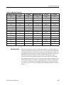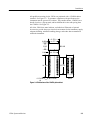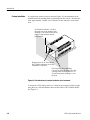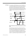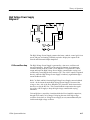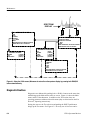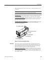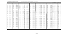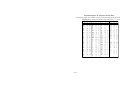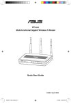
1
Instruction Manual
1705A
Spectrum Monitor (SN B040000 and Above)
070-8222-08
Warning
The servicing instructions are for use by qualified
personnel only. To avoid personal injury, do not
perform any servicing unless you are qualified to
do so. Refer to all safety summaries prior to
performing service.
www.tektronix.com
Test Equipment Depot - 800.517.8431 - 99 Washington Street Melrose, MA 02176 - FAX 781.665.0780 - TestEquipmentDepot.com
Table of Contents
General Safety Summary . . . . . . . . . . . . . . . . . . . . . . . . . . . . . . . . . . . . . . . . . . . . . .
Service Safety Summary . . . . . . . . . . . . . . . . . . . . . . . . . . . . . . . . . . . . . . . . . . . . . .
Preface . . . . . . . . . . . . . . . . . . . . . . . . . . . . . . . . . . . . . . . . . . . . . . . . . . . . . . . . . . . . .
Contacting Tektronix
ix
xi
xiii
xv
Introduction
Section 1 Introduction . . . . . . . . . . . . . . . . . . . . . . . . . . . . . . . . . . . . . . . . . . . . . . . .
1--1
Typical Configurations . . . . . . . . . . . . . . . . . . . . . . . . . . . . . . . . . . . . . . . . . . . . . . . . . . .
Options . . . . . . . . . . . . . . . . . . . . . . . . . . . . . . . . . . . . . . . . . . . . . . . . . . . . . . . . . . . . . . .
Accessories . . . . . . . . . . . . . . . . . . . . . . . . . . . . . . . . . . . . . . . . . . . . . . . . . . . . . . . . . . . .
Standard Accessories . . . . . . . . . . . . . . . . . . . . . . . . . . . . . . . . . . . . . . . . . . . . . . . . .
Optional Accessories . . . . . . . . . . . . . . . . . . . . . . . . . . . . . . . . . . . . . . . . . . . . . . . . .
Safety Information . . . . . . . . . . . . . . . . . . . . . . . . . . . . . . . . . . . . . . . . . . . . . . . . . . . . . .
ELECTRICAL SPECIFICATION . . . . . . . . . . . . . . . . . . . . . . . . . . . . . . . . . . . . . . . . . .
APPLICATIONS . . . . . . . . . . . . . . . . . . . . . . . . . . . . . . . . . . . . . . . . . . . . . . . . . . . . . . . .
Locating Satellites . . . . . . . . . . . . . . . . . . . . . . . . . . . . . . . . . . . . . . . . . . . . . . . . . . .
Satellite Footprints . . . . . . . . . . . . . . . . . . . . . . . . . . . . . . . . . . . . . . . . . . . . . . . . . . .
Using the 1705A for Satellite Communication . . . . . . . . . . . . . . . . . . . . . . . . . . . . . . . .
L-- Band Input Signals . . . . . . . . . . . . . . . . . . . . . . . . . . . . . . . . . . . . . . . . . . . . . . . . . . . .
Zeroing in on a Satellite . . . . . . . . . . . . . . . . . . . . . . . . . . . . . . . . . . . . . . . . . . . . . . . . . .
Locating the Satellite . . . . . . . . . . . . . . . . . . . . . . . . . . . . . . . . . . . . . . . . . . . . . . . . .
Identifying the Satellite . . . . . . . . . . . . . . . . . . . . . . . . . . . . . . . . . . . . . . . . . . . . . . .
Finding The Correct Transponder . . . . . . . . . . . . . . . . . . . . . . . . . . . . . . . . . . . . . . .
Optimize Signal Strength . . . . . . . . . . . . . . . . . . . . . . . . . . . . . . . . . . . . . . . . . . . . . .
Looking at Exciters with the 70 MHz Input . . . . . . . . . . . . . . . . . . . . . . . . . . . . . . .
Miscellaneous Uses for the 1705A . . . . . . . . . . . . . . . . . . . . . . . . . . . . . . . . . . . . . . . . . .
1-- 1
1-- 2
1-- 2
1-- 2
1-- 3
1-- 3
1-- 4
1-- 9
1-- 9
1-- 10
1-- 11
1-- 12
1-- 13
1-- 13
1-- 13
1-- 15
1-- 15
1-- 16
1-- 17
Operating Instructions
Section 2 Operating Instructions . . . . . . . . . . . . . . . . . . . . . . . . . . . . . . . . . . . . . . .
2--1
Front-panel Controls and Indicators . . . . . . . . . . . . . . . . . . . . . . . . . . . . . . . . . . . . . . . . .
FILTER . . . . . . . . . . . . . . . . . . . . . . . . . . . . . . . . . . . . . . . . . . . . . . . . . . . . . . . . . . . .
INPUT . . . . . . . . . . . . . . . . . . . . . . . . . . . . . . . . . . . . . . . . . . . . . . . . . . . . . . . . . . . .
SWEEP . . . . . . . . . . . . . . . . . . . . . . . . . . . . . . . . . . . . . . . . . . . . . . . . . . . . . . . . . . . .
DISPLAY . . . . . . . . . . . . . . . . . . . . . . . . . . . . . . . . . . . . . . . . . . . . . . . . . . . . . . . . . .
POSITION . . . . . . . . . . . . . . . . . . . . . . . . . . . . . . . . . . . . . . . . . . . . . . . . . . . . . . . . .
POWER . . . . . . . . . . . . . . . . . . . . . . . . . . . . . . . . . . . . . . . . . . . . . . . . . . . . . . . . . . .
Rear-- Panel Connectors . . . . . . . . . . . . . . . . . . . . . . . . . . . . . . . . . . . . . . . . . . . . . . . . . . .
INPUTS . . . . . . . . . . . . . . . . . . . . . . . . . . . . . . . . . . . . . . . . . . . . . . . . . . . . . . . . . . .
POWER . . . . . . . . . . . . . . . . . . . . . . . . . . . . . . . . . . . . . . . . . . . . . . . . . . . . . . . . . . .
Powering-- up . . . . . . . . . . . . . . . . . . . . . . . . . . . . . . . . . . . . . . . . . . . . . . . . . . . . . . . . . . .
Measurement Graticule . . . . . . . . . . . . . . . . . . . . . . . . . . . . . . . . . . . . . . . . . . . . . . . . . . .
2-- 1
2-- 1
2-- 1
2-- 2
2-- 3
2-- 4
2-- 4
2-- 4
2-- 4
2-- 5
2-- 6
2-- 7
1705A Spectrum Monitor
i
Table of Contents
Vertical Scales . . . . . . . . . . . . . . . . . . . . . . . . . . . . . . . . . . . . . . . . . . . . . . . . . . . . . .
Horizontal Scales . . . . . . . . . . . . . . . . . . . . . . . . . . . . . . . . . . . . . . . . . . . . . . . . . . . .
Center Frequency Readout . . . . . . . . . . . . . . . . . . . . . . . . . . . . . . . . . . . . . . . . . . . . . . . .
Customizing Frequency Readout . . . . . . . . . . . . . . . . . . . . . . . . . . . . . . . . . . . . . . . . . . .
Turning On or Off Readout . . . . . . . . . . . . . . . . . . . . . . . . . . . . . . . . . . . . . . . . . . . .
Changing Readout Position . . . . . . . . . . . . . . . . . . . . . . . . . . . . . . . . . . . . . . . . . . . .
Changing Readout Frequency . . . . . . . . . . . . . . . . . . . . . . . . . . . . . . . . . . . . . . . . . .
Test Mode . . . . . . . . . . . . . . . . . . . . . . . . . . . . . . . . . . . . . . . . . . . . . . . . . . . . . . . . . .
Locating Ku-- Band Satellites . . . . . . . . . . . . . . . . . . . . . . . . . . . . . . . . . . . . . . . . . . . . . .
Basic Operating Procedure . . . . . . . . . . . . . . . . . . . . . . . . . . . . . . . . . . . . . . . . . . . .
2-- 7
2-- 9
2-- 11
2-- 14
2-- 14
2-- 14
2-- 15
2-- 17
2-- 17
2-- 17
Section 3 Installation . . . . . . . . . . . . . . . . . . . . . . . . . . . . . . . . . . . . . . . . . . . . . . . . .
3--1
Packaging . . . . . . . . . . . . . . . . . . . . . . . . . . . . . . . . . . . . . . . . . . . . . . . . . . . . . . . . . .
Electrical Installation . . . . . . . . . . . . . . . . . . . . . . . . . . . . . . . . . . . . . . . . . . . . . . . . . . . .
Power Source . . . . . . . . . . . . . . . . . . . . . . . . . . . . . . . . . . . . . . . . . . . . . . . . . . . . . . .
Mains Frequency and Voltage Ranges . . . . . . . . . . . . . . . . . . . . . . . . . . . . . . . . . . . .
+18 Volts For Block Down Converter . . . . . . . . . . . . . . . . . . . . . . . . . . . . . . . . . . . .
Operating Options . . . . . . . . . . . . . . . . . . . . . . . . . . . . . . . . . . . . . . . . . . . . . . . . . . .
Mechanical Installation . . . . . . . . . . . . . . . . . . . . . . . . . . . . . . . . . . . . . . . . . . . . . . . . . . .
Cabinet Options . . . . . . . . . . . . . . . . . . . . . . . . . . . . . . . . . . . . . . . . . . . . . . . . . . . . .
Cabinetizing . . . . . . . . . . . . . . . . . . . . . . . . . . . . . . . . . . . . . . . . . . . . . . . . . . . . . . . .
Rack Adapter . . . . . . . . . . . . . . . . . . . . . . . . . . . . . . . . . . . . . . . . . . . . . . . . . . . . . . .
Custom Installation . . . . . . . . . . . . . . . . . . . . . . . . . . . . . . . . . . . . . . . . . . . . . . . . . .
3-- 1
3-- 1
3-- 1
3-- 1
3-- 1
3-- 2
3-- 2
3-- 2
3-- 4
3-- 5
3-- 8
Installation
Theory of Operation
ii
Section 4 Theory of Operation . . . . . . . . . . . . . . . . . . . . . . . . . . . . . . . . . . . . . . . . .
4--1
Overview . . . . . . . . . . . . . . . . . . . . . . . . . . . . . . . . . . . . . . . . . . . . . . . . . . . . . . . . . . . . . .
Block Diagram . . . . . . . . . . . . . . . . . . . . . . . . . . . . . . . . . . . . . . . . . . . . . . . . . . . . . . . . .
RF Input Circuits (Diagram 1) . . . . . . . . . . . . . . . . . . . . . . . . . . . . . . . . . . . . . . . . . .
IF Amplifier Circuits (Diagram 2) . . . . . . . . . . . . . . . . . . . . . . . . . . . . . . . . . . . . . . .
Sweep Generator Circuits (Diagram 3) . . . . . . . . . . . . . . . . . . . . . . . . . . . . . . . . . . .
Deflection Amplifiers (Diagram 4) . . . . . . . . . . . . . . . . . . . . . . . . . . . . . . . . . . . . . .
Microprocessor (Diagram 5) . . . . . . . . . . . . . . . . . . . . . . . . . . . . . . . . . . . . . . . . . . .
Front Panel (Diagram 6) . . . . . . . . . . . . . . . . . . . . . . . . . . . . . . . . . . . . . . . . . . . . . .
Low Voltage Power Supply (Diagram 7) . . . . . . . . . . . . . . . . . . . . . . . . . . . . . . . . . .
High Voltage (Diagram 8) . . . . . . . . . . . . . . . . . . . . . . . . . . . . . . . . . . . . . . . . . . . . .
RF Input
Diagram 1 . . . . . . . . . . . . . . . . . . . . . . . . . . . . . . . . . . . . . . . . . . . . . . . . . .
L-- Band Input . . . . . . . . . . . . . . . . . . . . . . . . . . . . . . . . . . . . . . . . . . . . . . . . . . . . . . .
70 MHz Input . . . . . . . . . . . . . . . . . . . . . . . . . . . . . . . . . . . . . . . . . . . . . . . . . . . . . . .
70 MHz Local Oscillator . . . . . . . . . . . . . . . . . . . . . . . . . . . . . . . . . . . . . . . . . . . . . .
IF Amplifier
Diagram 2 . . . . . . . . . . . . . . . . . . . . . . . . . . . . . . . . . . . . . . . . . . . . . . . . . .
2nd Local Oscillator . . . . . . . . . . . . . . . . . . . . . . . . . . . . . . . . . . . . . . . . . . . . . . . . . .
Input Filter, Mixer, and IF Amplifier . . . . . . . . . . . . . . . . . . . . . . . . . . . . . . . . . . . . .
Resolution Filter and Log Detector . . . . . . . . . . . . . . . . . . . . . . . . . . . . . . . . . . . . . .
Sweep Generator
Diagram 3 . . . . . . . . . . . . . . . . . . . . . . . . . . . . . . . . . . . . . . . . . . . . . . . . . .
4-- 1
4-- 1
4-- 1
4-- 2
4-- 2
4-- 3
4-- 3
4-- 3
4-- 3
4-- 4
4-- 4
4-- 4
4-- 4
4-- 5
4-- 5
4-- 5
4-- 6
4-- 6
4-- 7
1705A Spectrum Monitor
Table of Contents
Ramp Generator . . . . . . . . . . . . . . . . . . . . . . . . . . . . . . . . . . . . . . . . . . . . . . . . . . . . .
Gain Control (SPAN/DIV) . . . . . . . . . . . . . . . . . . . . . . . . . . . . . . . . . . . . . . . . . . . . .
Sweep Shapers . . . . . . . . . . . . . . . . . . . . . . . . . . . . . . . . . . . . . . . . . . . . . . . . . . . . . .
Bright-- Up Generator . . . . . . . . . . . . . . . . . . . . . . . . . . . . . . . . . . . . . . . . . . . . . . . . .
Z-- Axis Control . . . . . . . . . . . . . . . . . . . . . . . . . . . . . . . . . . . . . . . . . . . . . . . . . . . . .
Deflection Amplifiers
Diagram 4 . . . . . . . . . . . . . . . . . . . . . . . . . . . . . . . . . . . . . . . . . . . . . . . . . .
Buffers . . . . . . . . . . . . . . . . . . . . . . . . . . . . . . . . . . . . . . . . . . . . . . . . . . . . . . . . . . . .
Vertical Deflection Amplifier . . . . . . . . . . . . . . . . . . . . . . . . . . . . . . . . . . . . . . . . . .
Horizontal Deflection Amplifier . . . . . . . . . . . . . . . . . . . . . . . . . . . . . . . . . . . . . . . .
Microprocessor
Diagram 5 . . . . . . . . . . . . . . . . . . . . . . . . . . . . . . . . . . . . . . . . . . . . . . . . . .
Microprocessor . . . . . . . . . . . . . . . . . . . . . . . . . . . . . . . . . . . . . . . . . . . . . . . . . . . . . .
Readout . . . . . . . . . . . . . . . . . . . . . . . . . . . . . . . . . . . . . . . . . . . . . . . . . . . . . . . . . . .
Trace Rotate . . . . . . . . . . . . . . . . . . . . . . . . . . . . . . . . . . . . . . . . . . . . . . . . . . . . . . . .
Graticule Lights . . . . . . . . . . . . . . . . . . . . . . . . . . . . . . . . . . . . . . . . . . . . . . . . . . . . .
Front Panel
Diagram 6 . . . . . . . . . . . . . . . . . . . . . . . . . . . . . . . . . . . . . . . . . . . . . . . . . .
Indicators, Controls, and Switches . . . . . . . . . . . . . . . . . . . . . . . . . . . . . . . . . . . . . .
+18 Volt Supply . . . . . . . . . . . . . . . . . . . . . . . . . . . . . . . . . . . . . . . . . . . . . . . . . . . . .
Low Voltage Power Supply
Diagram 7 . . . . . . . . . . . . . . . . . . . . . . . . . . . . . . . . . . . . . . . . . . . . . . . . . .
Line Rectifier and Filter . . . . . . . . . . . . . . . . . . . . . . . . . . . . . . . . . . . . . . . . . . . . . .
Pulse Width Modulator . . . . . . . . . . . . . . . . . . . . . . . . . . . . . . . . . . . . . . . . . . . . . . .
Output Filters . . . . . . . . . . . . . . . . . . . . . . . . . . . . . . . . . . . . . . . . . . . . . . . . . . . . . . .
Error Amplifier . . . . . . . . . . . . . . . . . . . . . . . . . . . . . . . . . . . . . . . . . . . . . . . . . . . . .
Feedback Transformer Driver and Peak Detector . . . . . . . . . . . . . . . . . . . . . . . . . . .
Output Under-Voltage Shutdown . . . . . . . . . . . . . . . . . . . . . . . . . . . . . . . . . . . . . . . .
High Voltage Power Supply
Diagram 8 . . . . . . . . . . . . . . . . . . . . . . . . . . . . . . . . . . . . . . . . . . . . . . . . . .
HV Osc and Error Amp . . . . . . . . . . . . . . . . . . . . . . . . . . . . . . . . . . . . . . . . . . . . . . .
Power Supply Outputs . . . . . . . . . . . . . . . . . . . . . . . . . . . . . . . . . . . . . . . . . . . . . . . .
Focus Amplifier . . . . . . . . . . . . . . . . . . . . . . . . . . . . . . . . . . . . . . . . . . . . . . . . . . . . .
Grid Drive Circuit . . . . . . . . . . . . . . . . . . . . . . . . . . . . . . . . . . . . . . . . . . . . . . . . . . .
Z-Axis Amplifier . . . . . . . . . . . . . . . . . . . . . . . . . . . . . . . . . . . . . . . . . . . . . . . . . . . .
4-- 7
4-- 7
4-- 7
4-- 8
4-- 9
4-- 9
4-- 9
4-- 10
4-- 10
4-- 11
4-- 11
4-- 12
4-- 12
4-- 12
4-- 12
4-- 12
4-- 13
4-- 14
4-- 15
4-- 15
4-- 16
4-- 16
4-- 16
4-- 16
4-- 17
4-- 17
4-- 18
4-- 18
4-- 18
4-- 18
Checks and Adjustments
Section 5 Checks And Adjustments . . . . . . . . . . . . . . . . . . . . . . . . . . . . . . . . . . . . .
5--1
Recommended Equipment List . . . . . . . . . . . . . . . . . . . . . . . . . . . . . . . . . . . . . . . . . . . . .
Electrical Instruments . . . . . . . . . . . . . . . . . . . . . . . . . . . . . . . . . . . . . . . . . . . . . . . .
Auxiliary Equipment . . . . . . . . . . . . . . . . . . . . . . . . . . . . . . . . . . . . . . . . . . . . . . . . .
Performance Check . . . . . . . . . . . . . . . . . . . . . . . . . . . . . . . . . . . . . . . . . . . . . . . . . . . . . .
Short-Form Procedure . . . . . . . . . . . . . . . . . . . . . . . . . . . . . . . . . . . . . . . . . . . . . . . .
Long Form Procedure . . . . . . . . . . . . . . . . . . . . . . . . . . . . . . . . . . . . . . . . . . . . . . . .
Adjustment Procedure . . . . . . . . . . . . . . . . . . . . . . . . . . . . . . . . . . . . . . . . . . . . . . . . . . . .
5-- 1
5-- 1
5-- 2
5-- 3
5-- 3
5-- 5
5-- 17
1705A Spectrum Monitor
iii
Table of Contents
Short-- Form Procedure . . . . . . . . . . . . . . . . . . . . . . . . . . . . . . . . . . . . . . . . . . . . . . . .
Long Form Procedure . . . . . . . . . . . . . . . . . . . . . . . . . . . . . . . . . . . . . . . . . . . . . . . .
5-- 17
5-- 18
Maintenance . . . . . . . . . . . . . . . . . . . . . . . . . . . . . . . . . . . . . . . . . . 6- - 1
Section 6 Maintenance . . . . . . . . . . . . . . . . . . . . . . . . . . . . . . . . . . . . . . . . . . . . . . . .
6--1
PREVENTIVE MAINTENANCE . . . . . . . . . . . . . . . . . . . . . . . . . . . . . . . . . . . . . . . . . .
Cleaning . . . . . . . . . . . . . . . . . . . . . . . . . . . . . . . . . . . . . . . . . . . . . . . . . . . . . . . . . . .
Visual Inspection . . . . . . . . . . . . . . . . . . . . . . . . . . . . . . . . . . . . . . . . . . . . . . . . . . . .
Static-- Sensitive Components . . . . . . . . . . . . . . . . . . . . . . . . . . . . . . . . . . . . . . . . . .
Performance Checks and Readjustments . . . . . . . . . . . . . . . . . . . . . . . . . . . . . . . . . .
TROUBLESHOOTING . . . . . . . . . . . . . . . . . . . . . . . . . . . . . . . . . . . . . . . . . . . . . . . . . .
Diagnostic Routines . . . . . . . . . . . . . . . . . . . . . . . . . . . . . . . . . . . . . . . . . . . . . . . . . . . . .
Memory Test . . . . . . . . . . . . . . . . . . . . . . . . . . . . . . . . . . . . . . . . . . . . . . . . . . . . . . .
DAC Test . . . . . . . . . . . . . . . . . . . . . . . . . . . . . . . . . . . . . . . . . . . . . . . . . . . . . . . . . .
LED and Key Tests . . . . . . . . . . . . . . . . . . . . . . . . . . . . . . . . . . . . . . . . . . . . . . . . . .
Troubleshooting Aids . . . . . . . . . . . . . . . . . . . . . . . . . . . . . . . . . . . . . . . . . . . . . . . . . . . .
Foldout Pages . . . . . . . . . . . . . . . . . . . . . . . . . . . . . . . . . . . . . . . . . . . . . . . . . . . . . . .
Parts Lists . . . . . . . . . . . . . . . . . . . . . . . . . . . . . . . . . . . . . . . . . . . . . . . . . . . . . . . . . .
Major Assembly Interconnection . . . . . . . . . . . . . . . . . . . . . . . . . . . . . . . . . . . . . . . .
General Troubleshooting Techniques . . . . . . . . . . . . . . . . . . . . . . . . . . . . . . . . . . . .
Power Supply Troubleshooting Procedure . . . . . . . . . . . . . . . . . . . . . . . . . . . . . . . . . . . .
Introduction . . . . . . . . . . . . . . . . . . . . . . . . . . . . . . . . . . . . . . . . . . . . . . . . . . . . . . . .
Low Volts Supply . . . . . . . . . . . . . . . . . . . . . . . . . . . . . . . . . . . . . . . . . . . . . . . . . . . .
High Volts Supply . . . . . . . . . . . . . . . . . . . . . . . . . . . . . . . . . . . . . . . . . . . . . . . . . . .
CORRECTIVE MAINTENANCE . . . . . . . . . . . . . . . . . . . . . . . . . . . . . . . . . . . . . . . . . .
Obtaining Replacement Parts . . . . . . . . . . . . . . . . . . . . . . . . . . . . . . . . . . . . . . . . . . . . . .
Test Selected Components . . . . . . . . . . . . . . . . . . . . . . . . . . . . . . . . . . . . . . . . . . . . .
Mechanical Disassembly/Assembly . . . . . . . . . . . . . . . . . . . . . . . . . . . . . . . . . . . . . . . . .
Bezel Removal . . . . . . . . . . . . . . . . . . . . . . . . . . . . . . . . . . . . . . . . . . . . . . . . . . . . . .
Graticule Light Removal and Replacement . . . . . . . . . . . . . . . . . . . . . . . . . . . . . . .
Removal of the CRT . . . . . . . . . . . . . . . . . . . . . . . . . . . . . . . . . . . . . . . . . . . . . . . . .
Replacing the CRT . . . . . . . . . . . . . . . . . . . . . . . . . . . . . . . . . . . . . . . . . . . . . . . . . . .
Removal of the Rear Panel . . . . . . . . . . . . . . . . . . . . . . . . . . . . . . . . . . . . . . . . . . . .
Removal of Front-- Panel Assembly . . . . . . . . . . . . . . . . . . . . . . . . . . . . . . . . . . . . . .
Removing the L-- Band Tuner . . . . . . . . . . . . . . . . . . . . . . . . . . . . . . . . . . . . . . . . . .
Removing the 70 MHz Tuner . . . . . . . . . . . . . . . . . . . . . . . . . . . . . . . . . . . . . . . . . .
Removal and Replacement of the Main Board . . . . . . . . . . . . . . . . . . . . . . . . . . . . .
Removal and Replacement of the Power Supply Board . . . . . . . . . . . . . . . . . . . . . .
Removing the LNB Power Supply Board . . . . . . . . . . . . . . . . . . . . . . . . . . . . . . . . .
REPACKAGING . . . . . . . . . . . . . . . . . . . . . . . . . . . . . . . . . . . . . . . . . . . . . . . . . . . . . . . .
6-- 1
6-- 1
6-- 2
6-- 2
6-- 3
6-- 3
6-- 4
6-- 5
6-- 7
6-- 8
6-- 8
6-- 8
6-- 9
6-- 10
6-- 10
6-- 12
6-- 12
6-- 13
6-- 15
6-- 18
6-- 18
6-- 18
6-- 19
6-- 19
6-- 20
6-- 21
6-- 21
6-- 22
6-- 22
6-- 23
6-- 24
6-- 24
6-- 25
6-- 26
6-- 27
Section 7 Options . . . . . . . . . . . . . . . . . . . . . . . . . . . . . . . . . . . . . . . . . . . . . . . . . . . .
7--1
Options . . . . . . . . . . . . . . . . . . . . . . . . . . . . . . . . . . . . . . . . . . . . . . . . . . . . . . . . . . . . . . .
Field Upgrade Kits . . . . . . . . . . . . . . . . . . . . . . . . . . . . . . . . . . . . . . . . . . . . . . . . . . . . . .
ORDERING . . . . . . . . . . . . . . . . . . . . . . . . . . . . . . . . . . . . . . . . . . . . . . . . . . . . . . . . . . .
7-- 1
7-- 1
7-- 2
Options
iv
1705A Spectrum Monitor
Table of Contents
Replaceable Electrical Parts
Section 8 Replaceable Electrical Parts . . . . . . . . . . . . . . . . . . . . . . . . . . . . . . . . . . .
8--1
Parts Ordering Information . . . . . . . . . . . . . . . . . . . . . . . . . . . . . . . . . . . . . . . . . . . . . . . .
Using the Replaceable Electrical Parts List . . . . . . . . . . . . . . . . . . . . . . . . . . . . . . . . . . .
Cross Index-- Mfr. Code Number to Manufacturer . . . . . . . . . . . . . . . . . . . . . . . . . . .
Abbreviations . . . . . . . . . . . . . . . . . . . . . . . . . . . . . . . . . . . . . . . . . . . . . . . . . . . . . . .
List of Assemblies . . . . . . . . . . . . . . . . . . . . . . . . . . . . . . . . . . . . . . . . . . . . . . . . . . .
Column Descriptions . . . . . . . . . . . . . . . . . . . . . . . . . . . . . . . . . . . . . . . . . . . . . . . . . . . . .
Component No. (Column 1) . . . . . . . . . . . . . . . . . . . . . . . . . . . . . . . . . . . . . . . . .
Tektronix Part No. (Column 2) . . . . . . . . . . . . . . . . . . . . . . . . . . . . . . . . . . . . . . . . .
Serial/Assembly No. (Column 3 and 4) . . . . . . . . . . . . . . . . . . . . . . . . . . . . . . . . . . .
Name and Description (Column 5) . . . . . . . . . . . . . . . . . . . . . . . . . . . . . . . . . . . . . .
Mfr. Code (Column 6) . . . . . . . . . . . . . . . . . . . . . . . . . . . . . . . . . . . . . . . .
Mfr. Part No. (Column 7) . . . . . . . . . . . . . . . . . . . . . . . . . . . . . . . . . . . . . . . . . . . . . .
8-- 1
8-- 1
8-- 1
8-- 1
8-- 1
8-- 2
8-- 2
8-- 2
8-- 2
8-- 2
8-- 2
8-- 2
Diagrams/Circuit Board Illustrations
Replaceable Mechanical Parts
Section 10 Replaceable Mechanical Parts . . . . . . . . . . . . . . . . . . . . . . . . . . . . . . . .
10--1
Parts Ordering Information . . . . . . . . . . . . . . . . . . . . . . . . . . . . . . . . . . . . . . . . . . . . . . . .
Using the Replaceable Mechanical Parts List . . . . . . . . . . . . . . . . . . . . . . . . . . . . . . . . .
10-- 1
10-- 1
1705A Spectrum Monitor
v
Table of Contents
List of Figures
Figure 1-1: 1705A used to locate satellites and determine maximum signal level . . . . . . . . .
Figure 1-2: Relationship of a communications satellite to earth . . . . . . . . . . . . . . . . . . . . . . .
Figure 1-3: Angle A (the difference at a specific latitude between the angle to the sun
and the angle to a satellite) . . . . . . . . . . . . . . . . . . . . . . . . . . . . . . . . . . . . . . . . .
Figure 1-4: Sample longitudinal map of the Ku-Band satellites . . . . . . . . . . . . . . . . . . . . . . .
Figure 1-5: The western spot beam footprint for one Ku-Band satellite . . . . . . . . . . . . . . . . .
Figure 1-6: A computer representation of the 1705A display showing the 12.198 GHz
horizontally polarized telemetry beacon on the SATCOM K2 satellite . . . . . . . .
Figure 1-7: Transponder assignments for a typical Ku--Band, 16--transponder satellite
that employs alternate polarization . . . . . . . . . . . . . . . . . . . . . . . . . . . . . . . . . . . .
Figure 1-8: Simulation of a 1705A FULL SPAN/DIV display . . . . . . . . . . . . . . . . . . . . . . .
Figure 1-9: Up link Video Exciter, Up converter, and High Power Amplifier (HPA) showing
how to hook up a 1705A Spectrum Monitor to look at the Video Exciter output
Figure 1-10: 1705A hooked up to look at either the output of the Video Exciter (70 MHz)
or the Receiver Input (L-Band) . . . . . . . . . . . . . . . . . . . . . . . . . . . . . . . . . . . . . . .
vi
1--2
1--9
1--10
1--11
1--12
1--14
1--15
1--16
1--17
1--18
Figure 2-1: 1705A front panel . . . . . . . . . . . . . . . . . . . . . . . . . . . . . . . . . . . . . . . . . . . . . . . . .
Figure 2-2: 1705A rear panel controls and connectors . . . . . . . . . . . . . . . . . . . . . . . . . . . . . .
Figure 2-3: 1705A display when powered up in L-BAND and FULL SPAN . . . . . . . . . . . . .
Figure 2-4: 1705A graticule scale . . . . . . . . . . . . . . . . . . . . . . . . . . . . . . . . . . . . . . . . . . . . . .
Figure 2-5: Relationship of sweep to graticule showing minimum and maximum frequencies
Figure 2-6: Frequency relationship to horizontal graticule scale . . . . . . . . . . . . . . . . . . . . . . .
Figure 2-7: Center frequency cursor and readout for the L-Band with FULL SPAN/DIV . . .
Figure 2-8: 1705A CRT with the SCALE turned down . . . . . . . . . . . . . . . . . . . . . . . . . . . . .
Figure 2-9: The setting of the HORIZONTAL POSITION control can displace the location
of the displayed center frequency . . . . . . . . . . . . . . . . . . . . . . . . . . . . . . . . . . . . .
Figure 2-10: Using the 1705A menus . . . . . . . . . . . . . . . . . . . . . . . . . . . . . . . . . . . . . . . . . . .
Figure 2-11: An example of the readout displayed while satellite frequency is being set . . . .
2--2
2--5
2--6
2--7
2--10
2--11
2--12
2--13
2--13
2--15
2--16
Figure 3-1: L-BAND INPUT connector and controls . . . . . . . . . . . . . . . . . . . . . . . . . . . . . . .
Figure 3-2: Dimensions of the 1700F00 plain cabinet . . . . . . . . . . . . . . . . . . . . . . . . . . . . . . .
Figure 3-3: 1700F02 portable cabinet dimensions . . . . . . . . . . . . . . . . . . . . . . . . . . . . . . . . . .
Figure 3-4: Cabinet securing screws . . . . . . . . . . . . . . . . . . . . . . . . . . . . . . . . . . . . . . . . . . . .
Figure 3-5: The WFM7F05 side-by-side rack adapter . . . . . . . . . . . . . . . . . . . . . . . . . . . . . . .
Figure 3-6: A WFM7F05 with a blank front panel (1700F06) . . . . . . . . . . . . . . . . . . . . . . . .
Figure 3-7: WFM7F05 rack mount cabinet with a 1700F06 utility drawer . . . . . . . . . . . . . . .
3--2
3--3
3--4
3--5
3--5
3--6
3--7
1705A Spectrum Monitor
Table of Contents
Figure 3-8: Considerations for custom installation of an instrument . . . . . . . . . . . . . . . . . . . .
3--8
Figure 4-1: 1705A L--Band comb display showing the areas each of the six sweep shaper
variable resistors adjust . . . . . . . . . . . . . . . . . . . . . . . . . . . . . . . . . . . . . . . . . . . . .
Figure 4-2: Output duty cycle of the pulse width modulator used in the +18 V Power Supply
Figure 4-3: Pinout of the CRT Socket . . . . . . . . . . . . . . . . . . . . . . . . . . . . . . . . . . . . . . . . . . .
4--8
4--13
4--19
Figure 5-1: Initial equipment connections . . . . . . . . . . . . . . . . . . . . . . . . . . . . . . . . . . . . . . . .
Figure 5-2: Check time mark graticule alignment . . . . . . . . . . . . . . . . . . . . . . . . . . . . . . . . . .
Figure 5-3: Output of the SG503 connected directly to the 1705A 70 MHz INPUT . . . . . . .
Figure 5-4: Equipment connections for L--Band checkout . . . . . . . . . . . . . . . . . . . . . . . . . . .
Figure 5-5: Aligning L--Band time markers with the graticule lines . . . . . . . . . . . . . . . . . . . .
Figure 5-6: Using the UHF Signal Generator to check L--Band Span/Division, Readout, Gain,
and Flatness . . . . . . . . . . . . . . . . . . . . . . . . . . . . . . . . . . . . . . . . . . . . . . . . . . . . .
Figure 5-7: Adjustment locations . . . . . . . . . . . . . . . . . . . . . . . . . . . . . . . . . . . . . . . . . . . . . . .
Figure 5-8: DAC check waveforms used to check Focus, Astigmatism, Geometry, and setting
of the Trace Rotation . . . . . . . . . . . . . . . . . . . . . . . . . . . . . . . . . . . . . . . . . . . . . .
Figure 5-9: Location of the shorting strap used when adjusting sweep length . . . . . . . . . . . .
Figure 6-1: Using the 1705A menus . . . . . . . . . . . . . . . . . . . . . . . . . . . . . . . . . . . . . . . . . . . .
Figure 6-2: 1705A Test menu, displayed when Test is the Main menu selection . . . . . . . . . .
Figure 6-3: 1705A CRT display when the NOVRAM Test has been successfully completed
Figure 6-4: 1705A power up error message . . . . . . . . . . . . . . . . . . . . . . . . . . . . . . . . . . . . . . .
Figure 6-5: DAC check waveform . . . . . . . . . . . . . . . . . . . . . . . . . . . . . . . . . . . . . . . . . . . . .
Figure 6-6: Circuit board assembly locations . . . . . . . . . . . . . . . . . . . . . . . . . . . . . . . . . . . . .
Figure 6-7: Multiple pin connectors used in the 1705A Spectrum Monitor . . . . . . . . . . . . . .
Figure 6-8: Bezel securing screws . . . . . . . . . . . . . . . . . . . . . . . . . . . . . . . . . . . . . . . . . . . . . .
Figure 6-9: Screws securing the rear panel . . . . . . . . . . . . . . . . . . . . . . . . . . . . . . . . . . . . . . .
Figure 6-10: Screws securing the front panel board (A2) in place . . . . . . . . . . . . . . . . . . . . .
Figure 6-11: Screws holding the Main board (A3) and the Tuners (A5 and A6) in place . . . .
Figure 6-12: Removing the Power Supply board . . . . . . . . . . . . . . . . . . . . . . . . . . . . . . . . . . .
Figure 6-13: Mounting screws for the LNB Power Supply circuit board, A4 . . . . . . . . . . . . .
Figure 6-14: Repackaging a 1705A instrument . . . . . . . . . . . . . . . . . . . . . . . . . . . . . . . . . . . .
1705A Spectrum Monitor
5--6
5--8
5--9
5--12
5--13
5--14
5--19
5--20
5--21
6--4
6--5
6--6
6--7
6--8
6--9
6--11
6--20
6--22
6--23
6--24
6--26
6--26
6--27
vii
Table of Contents
List of Tables
viii
Table 1--1: Spectrum Display . . . . . . . . . . . . . . . . . . . . . . . . . . . . . . . . . . . . . . . . . . . . . . . . .
Table 1--2: CRT Display . . . . . . . . . . . . . . . . . . . . . . . . . . . . . . . . . . . . . . . . . . . . . . . . . . . . .
Table 1--3: Power Source . . . . . . . . . . . . . . . . . . . . . . . . . . . . . . . . . . . . . . . . . . . . . . . . . . . .
Table 1--4: Environmental Characteristics . . . . . . . . . . . . . . . . . . . . . . . . . . . . . . . . . . . . . . .
Table 1--5: Physical Characteristics . . . . . . . . . . . . . . . . . . . . . . . . . . . . . . . . . . . . . . . . . . . .
Table 1--6: Certifications and Compliances . . . . . . . . . . . . . . . . . . . . . . . . . . . . . . . . . . . . . .
1--4
1--5
1--5
1--6
1--6
1--6
Table 2--1: dB Reference . . . . . . . . . . . . . . . . . . . . . . . . . . . . . . . . . . . . . . . . . . . . . . . . . . . . .
Table 2--2: dBm to mv Conversion . . . . . . . . . . . . . . . . . . . . . . . . . . . . . . . . . . . . . . . . . . . .
Table 2--3: Azimuth / Elevation Table for 21 CONUS Cities . . . . . . . . . . . . . . . . . . . . . . . .
2--8
2--9
2--18
Table 3--1: Internal Jumper Selection . . . . . . . . . . . . . . . . . . . . . . . . . . . . . . . . . . . . . . . . . . .
3--2
Table 5--1: Preliminary Control Settings . . . . . . . . . . . . . . . . . . . . . . . . . . . . . . . . . . . . . . . . .
Table 5--2: Preliminary Control Settings . . . . . . . . . . . . . . . . . . . . . . . . . . . . . . . . . . . . . . . . .
5--6
5--18
Table 6--1: Static Susceptibility . . . . . . . . . . . . . . . . . . . . . . . . . . . . . . . . . . . . . . . . . . . . . . . .
Table 6--2: Power Supply Fault Symptoms . . . . . . . . . . . . . . . . . . . . . . . . . . . . . . . . . . . . . .
Table 6--3: Low Volts Supply Voltages . . . . . . . . . . . . . . . . . . . . . . . . . . . . . . . . . . . . . . . . .
Table 6--4: Control Circuit Test Points . . . . . . . . . . . . . . . . . . . . . . . . . . . . . . . . . . . . . . . . . .
Table 6--5: High Volts Supply Fault Symptoms . . . . . . . . . . . . . . . . . . . . . . . . . . . . . . . . . . .
Table 6--6: High Voltage Oscillator Test Points . . . . . . . . . . . . . . . . . . . . . . . . . . . . . . . . . . .
Table 6--7: Test Selectable Components . . . . . . . . . . . . . . . . . . . . . . . . . . . . . . . . . . . . . . . . .
6--2
6--12
6--13
6--15
6--16
6--17
6--19
Table 7--1: Power Cord Options . . . . . . . . . . . . . . . . . . . . . . . . . . . . . . . . . . . . . . . . . . . . . . .
7--1
1705A Spectrum Monitor
General Safety Summary
Review the following safety precautions to avoid injury and prevent damage to
this product or any products connected to it. To avoid potential hazards, use this
product only as specified.
Only qualified personnel should perform service procedures.
While using this product, you may need to access other parts of the system. Read
the General Safety Summary in other system manuals for warnings and cautions
related to operating the system.
To Avoid Fire or
Personal Injury
Use Proper Power Cord. Use only the power cord specified for this product and
certified for the country of use.
Connect and Disconnect Properly. Do not connect or disconnect probes or test
leads while they are connected to a voltage source.
Ground the Product. This product is grounded through the grounding conductor
of the power cord. To avoid electric shock, the grounding conductor must be
connected to earth ground. Before making connections to the input or output
terminals of the product, ensure that the product is properly grounded.
Observe All Terminal Ratings. To avoid fire or shock hazard, observe all ratings
and markings on the product. Consult the product manual for further ratings
information before making connections to the product.
Connect the ground lead of the probe to earth ground only.
Do not apply a potential to any terminal, including the common terminal, that
exceeds the maximum rating of that terminal.
Do Not Operate Without Covers. Do not operate this product with covers or panels
removed.
Use Proper Fuse. Use only the fuse type and rating specified for this product.
Avoid Exposed Circuitry. Do not touch exposed connections and components
when power is present.
Wear Eye Protection. Wear eye protection if exposure to high-intensity rays or
laser radiation exists.
Do Not Operate With Suspected Failures. If you suspect there is damage to this
product, have it inspected by qualified service personnel.
Do Not Operate in Wet/Damp Conditions.
Do Not Operate in an Explosive Atmosphere.
Keep Product Surfaces Clean and Dry.
1705A Spectrum Monitor
ix
General Safety Summary
Provide Proper Ventilation. Refer to the manual’s installation instructions for
details on installing the product so it has proper ventilation.
Symbols and Terms
Terms in this Manual. These terms may appear in this manual:
WARNING. Warning statements identify conditions or practices that could result
in injury or loss of life.
CAUTION. Caution statements identify conditions or practices that could result in
damage to this product or other property.
Terms on the Product. These terms may appear on the product:
DANGER indicates an injury hazard immediately accessible as you read the
marking.
WARNING indicates an injury hazard not immediately accessible as you read the
marking.
CAUTION indicates a hazard to property including the product.
Symbols on the Product. The following symbols may appear on the product:
CAUTION
Refer to Manual
x
WARNING
High Voltage
Double
Insulated
Protective Ground
(Earth) Terminal
Not suitable for
connection to
the public telecommunications network
1705A Spectrum Monitor
Service Safety Summary
Only qualified personnel should perform service procedures. Read this Service
Safety Summary and the General Safety Summary before performing any service
procedures.
Do Not Service Alone. Do not perform internal service or adjustments of this
product unless another person capable of rendering first aid and resuscitation is
present.
Disconnect Power. To avoid electric shock, switch off the instrument power, then
disconnect the power cord from the mains power.
Use Caution When Servicing the CRT. To avoid electric shock or injury, use
extreme caution when handling the CRT. Only qualified personnel familiar with
CRT servicing procedures and precautions should remove or install the CRT.
CRTs retain hazardous voltages for long periods of time after power is turned off.
Before attempting any servicing, discharge the CRT by shorting the anode to
chassis ground. When discharging the CRT, connect the discharge path to ground
and then the anode. Rough handling may cause the CRT to implode. Do not nick
or scratch the glass or subject it to undue pressure when removing or installing it.
When handling the CRT, wear safety goggles and heavy gloves for protection.
Use Care When Servicing With Power On. Dangerous voltages or currents may
exist in this product. Disconnect power, remove battery (if applicable), and
disconnect test leads before removing protective panels, soldering, or replacing
components.
To avoid electric shock, do not touch exposed connections.
X-Radiation. To avoid x-radiation exposure, do not modify or otherwise alter the
high-voltage circuitry or the CRT enclosure. X-ray emissions generated within
this product have been sufficiently shielded.
1705A Spectrum Monitor
xi
Service Safety Summary
xii
1705A Spectrum Monitor
Preface
The information in this manual is intended for instrument operators and service
technicians. Operators are assumed to befamiliar with basic television terms and
measurements. Qualified service technicians are also assumed to be familiar with
television terms and measurements, and have moderate experience with analog
and logic circuits.
The manual is divided into two parts: Operator’s Information and Service
Information. The Operator’s Information is useful to both operators and service
technicians. The Service Information is intended only for qualified service
technicians.
Section 1, Introduction
Section 1, Introduction, includes a general description of the instrument followed
by the Specifications. The Specifications include references to the corresponding Performance check steps.
Section 2, Operating
Instructions
Section 2, Operating Instructions, familiarizes the user with the front-- and
rear--panel controls, connectors, and indicators; includes an operator’s check-out
procedure; and includes other operator familiarization information.
Section 3, Installation
Section 3, Installation, includes electrical and mechanical installation information. The electrical installation information includes adjustments and operational
changes available with the instrument. The mechanical installation information
includes rackmounting, custom installation, and portable use.
Section 4, Theory of
Operation
Section 4, Theory of Operation, provides an over-all block diagram description and
detailed circuit descriptions. Read the block diagram description for an overview of the
instrument. The detailed circuit descriptions should be used with the block diagram and
schematic diagrams in the foldout pages for specific information about individual
circuits.
Section 5, Checks and
Adjustments
Section 5, Checks and Adjustments, includes the Performance Check Procedure and the
Adjustment Procedure. The Performance Check Procedure is used to verify that the
instrument’s performance is within its specifications, and the Adjustment Procedure is
used to adjust the instrument to meet its specifications. The procedures are preceded by
a list of recommended test equipment. Each procedure has a short form listing of the
individual steps.
Section 6, Maintenance
1705A Spectrum Monitor
Section 6, Maintenance, includes preventive, troubleshooting, and corrective
information.
xiii
Preface
Section 7, Options
Section 8, Replaceable
Electrical Parts
Section 9, Diagrams
Section 10, Replaceable
Mechanical Parts
xiv
Section 7, Options, documents instrument options. The information in this
section summarizes the options. Additional details are included in appro-priate
places throughout the manual.
Section 8, Replaceable Electrical Parts, includes order information and part
numbers for all replaceable electrical parts.
Section 9, Diagrams, contains servicing illustra-tions. These include adjustment
locations, circuit board part locations, a block diagram, and schematic diagrams.
Parts locating tables are included that cross--reference the circuit board illustrations to the schematic diagrams.
Section 10, Replaceable Mechanical Parts, includes ordering information and
part numbers for all replaceable mechanical parts. This parts list is referenced to
an exploded view mechanical drawing. Also included are lists of accessories and
optional accessories.
1705A Spectrum Monitor
Preface
Contacting Tektronix
Phone
1-800-833-9200*
Address
Tektronix, Inc.
Department or name (if known)
14200 SW Karl Braun Drive
P.O. Box 500
Beaverton, OR 97077
USA
Web site
www.tektronix.com
Sales support
1-800-833-9200, select option 1*
Service support
1-800-833-9200, select option 2*
Technical support
Email: [email protected]
1-800-833-9200, select option 3*
6:00 a.m. - 5:00 p.m. Pacific time
*
1705A Spectrum Monitor
This phone number is toll free in North America. After office hours, please leave a
voice mail message.
Outside North America, contact a Tektronix sales office or distributor; see the
Tektronix web site for a list of offices.
xv
Preface
xvi
1705A Spectrum Monitor
Introduction
Section 1
Introduction
The TEKTRONIX 1705A Spectrum Monitor is an 8½” wide by 5¼” high
special purpose spectrum analyzer. It weighs approximately 8½ pounds and is
powered from an ac source. The crt occupies approximately two-thirds of the
front-panel area, with the control panel taking up the remainder of the space.
Operation is controlled by a microprocessor that polls the front-panel switches.
Front-panel switches are of the momentary touch type with lighted functional
indicators. In addition to polling the front panel, the microprocessor provides
the characters for an alphanumeric crt readout.
The signal is displayed on a bright crt. It is of the mesh type, for better
geometry, and uses an internal graticule to reduce parallax. Variable graticule
scale illumination provides even lighting over the usable graticule area to
improve measurement accuracy and the quality of display photographs.
The 1705A Spectrum Monitor is a swept front-end superheterodyne-type
spectrum analyzer with two inputs; L--Band to accommodate Low-Noise
Amplifier/Block Down Converter (LNB) outputs, and 70 MHz for use with
Video Exciters. The L--Band input (950 to 1800 MHz) is through an F-type
connector, while the 70 MHz input is through a standard bnc connector. The
L--BAND INPUT connector is the output for the selectable 18 V supply that is
the Block Down Converter auxiliary power.
Typical Configurations
The TEKTRONIX 1705A Spectrum Monitor is designed primarily for use in
locating satellites and monitoring their signals. It is designed so that it can be
rack mounted, in a dual-width rack adapter, along with a half-rack waveform
monitor, such as a TEKTRONIX 1740-Series Waveform/Vector Monitor.
However, it can be used as a portable instrument. It is intended to be connected
to the rf feed with a directional connector. See Figure 1-1. It is capable of
providing the dc power required to run an LNB. The auxiliary LNB power is
turned on or off by a rear-panel slide switch. An indicator on the rear panel
lights when the +18 V supply is operating normally.
1705A Spectrum Monitor
1- 1
Introduction
LOW-NOISE AMPLIFIER/
BLOCK DOWN CONVERTER
1705A
SPECTRUM MONITOR
RECEIVER
Figure 1-1: 1705A used to locate satellites and determine maximum signal level
Options
The only options currently available for the 1705A Spectrum Monitor are the
power plug options described in Section 7 (Options). If no power cord options
are ordered, instruments are shipped with the North American 125 V power cord
and one replacement fuse.
Accessories
Standard Accessories
1 Manual, Instruction
1 Adapter, F--type Male connector to BNC female connector
1 Power Cord, with the correct plug for the selected power plug option
1 Replacement Cartridge Fuse (correct rating for the power plug option)
3 Replacement Scale Illumination Bulbs (Tektronix P/N 150-0168-00 or ANSI
#73)
1- 2
1705A Spectrum Monitor
Introduction
Optional Accessories
Camera, C9 (Option 20)
Viewing Hood (016-0475-00)
Front Panel Cover (200-3897-01)
1700F00, Plain Cabinet (painted silver grey)
1700F02, Portable Cabinet (painted silver grey with handle, feet, and front
cover)
1700F05, Side-by-Side Rack Adapter
1700F06, Blank Half-Rack Width Panel
1700F07, Utility Drawer
Safety Information
The 1705A Spectrum Monitor is intended to operate from an ac power source
that will not apply more than 250 V rms between the supply conductors or
between either supply conductor and ground. A protective ground connection,
by way of the grounding conductor, is essential for safe operation.
The instrument was tested for compliance in a cabinet. To ensure continued
compliance, the instrument will need to be enclosed in a cabinet that is equivalent to those listed as Optional Accessories for the 1705A. A drawing of the
1700F00 plain cabinet is contained in the Installation Instructions (Section 3).
1705A Spectrum Monitor
1- 3
Introduction
ELECTRICAL SPECIFICATION
Table 1- 1: Spectrum Display
Characteristic
Frequency Range
L---Band
70 MHz
Performance
Requirements
950 to 1800 MHz
45 to 100 MHz
Frequency Span
L---Band
Full
10 MHz/Division
1 MHz/Division
100 kHz/Division
F---type connector
Bnc connector
10 Horiz. Div. Equals:
1000 MHz
100 MHz
10 MHz
1 MHz
11
10 Horiz. Div. Equals:
50 MHz
10 MHz
1 MHz
5
Typically 0.5 minor Division.
4, 5, 10, 11
Brightup offset by 1 Division in FULL
SPAN/DIV should still come on screen
in the next magnified position.
11
± from center (1400 MHz).
± from center (70 MHz).
12,
7
Typically ±1 dB /100 MHz.
12
Sweep Length
¶12 Divisions all SPANS/DIV settings.
4
Sweep Speed
Typically 20 --- 200 ms.
9
70 MHz
Full
1 MHz/Division
100 kHz/Division
Span/Div Accuracy
Flatness
L---Band ±5 dB.
70 MHz ±2 dB.
Maximum Signal Input
L---Band: ---30 dBm,
75Ω. 70 MHz:
---20 dBm, 75Ω..
Minimum Signal Input
---80 dBm.
Relative Amplitude Accuracy
L---Band (only)
±3 dB/100 MHz.
Positioning Range
Vertical
Horizontal
13
+ and ---3 Divisions.
+ and ---2 Divisions.
Displayed Frequencies in FULL
SPAN/DIV
L---BAND (900 --- 1900 MHz)
70 MHz (45 --- 100 MHz)
Left Grat. Mid Grat.
Edge
Line
900
1400
45
70
Frequency Readout
Center Frequency shown by time
sharing graphic readout. Exact position on the trace of the center frequency shown by a caret in all spans except
FULL.
1- 4
Check
Step
Supplemental Information
Right Grat.
Edge
1900
95
11
5
11
1705A Spectrum Monitor
Introduction
Table 1- 1: Spectrum Display (Cont.)
Characteristic
Performance
Requirements
Frequency Bright Up
Marker Registration
Readout Accuracy
Full Span has bright up and frequency
readout (without cursor). Bright-up
area will be on screen in at least the
next narrower span.
L---Band ±20 MHz.
70 MHz ±2 MHz
Resolution
6 dB Down
300 kHz
10 kHz
Check
Step
Supplemental Information
5
Typically ±10 MHz.
Typically ±1 MHz.
11
5
300 kHz ±1 Division at 100 kHz
Span/Div.
6
<2 minor Divisions at 100 kHz Span/
Div.
6
Reduces Video bandwidth to ¶10 kHz. 8
Video Filter
Low Noise Amplifier/Block Down
Converter dc Supply (LNB Power)
+18 Vdc ±5%. 250
mA max.
Output through L---BAND input
connector, switched on and off by
rear-panel slide switch. LED indicator
on rear panel.
3
2 dB Gain Accuracy
¶2 dB/Division.
<3 dB/Division at ---50 dBm.
14
Table 1- 2: CRT Display
Characteristic
Performance
Requirements
Crt Viewing Area
80 X 100 mm.
Accelerating Potential
13.75 kV.
Trace Rotation Range
Greater than ±1˚
from horizontal.
Graticule
Check
Step
Supplemental Information
Total adjustment range is typically 8˚.
Internal 8 X 10 Division spectrum
analyzer graticule with variable SCALE
illumination.
Table 1- 3: Power Source
Characteristic
Performance
Requirements
Mains Voltage Range
90---250 V.
Mains Frequency Range
48 Hz to 66 Hz.
Power Consumption
1705A Spectrum Monitor
Check
Step
Supplemental Information
Continuous range from 90 to 250 Vac.
2
35 Watts (120 BTU/HR) maximum.
1- 5
Introduction
Table 1- 4: Environmental Characteristics
Characteristic
Supplemental Information
Temperature
Non-Operating
Operating
---55˚C to +75˚C.
0˚C to +50˚C.
Altitude
Non-Operating
Operating
To 50,000 feet (15,000 meters).
To 15,000 feet (4,800 meters).
Vibration --- Operating
15 minutes each axis at 0.015”, frequency varied from 10---55---10 Hz in 1-minute
cycles with instrument secured to vibration platform. Ten minutes each axis at
any resonant point or at 55 Hz if no resonant point is found.
Shock --- Non-Operating
30 g’s, ½ sine, 11 ms duration, 3 shocks per surface (18 total).
Transportation
Qualified under NTSC Test Procedure 1A, Category II (30” drop).
Humidity
Will operate at 95% relative humidity for up to five days.
Table 1- 5: Physical Characteristics
Characteristic
Supplemental Information
Dimensions
Height
Width
Length
5 1/4 inches (133.4 mm).
8 1/2 inches (215.9 mm).
18 1/8 inches (460.4 mm).
Weight
Approximately 8.5 lbs (approximately 3.8 kg).
Table 1- 6: Certifications and Compliances
EC Declaration of Conformity EMC
Meets intent of Directive 89/336/EEC for Electromagnetic Compatibility. Compliance was
demonstrated to the following specifications as listed in the Official Journal of the European
Communities:
EN 50081-1 Emissions:
EN 55022
Class B Radiated and Conducted Emissions
EN 50082-1 Immunity:
IEC 801-2
Electrostatic Discharge Immunity
IEC 801-3
RF Electromagnetic Field Immunity
IEC 801-4
Electrical Fast Transient/Burst Immunity
High-quality shielded cables must be used to ensure compliance to the above listed standards.
This product complies when installed into any of the following Tektronix instrument enclosures:
1700F00 Standard Cabinet
1700F02 Portable Cabinet
1700F05 Rack Adapter
An increase of up to 20dB in the displayed noise floor may be observed if this instrument is
operated in electromagnetic fields of 3V/M or more, at frequencies of approximately 130, 250, 350,
or 490 MHz.
1- 6
1705A Spectrum Monitor
Test Equipment Depot - 800.517.8431 - 99 Washington Street Melrose, MA 02176 - FAX 781.665.0780 - TestEquipmentDepot.com
Introduction
Table 1- 6: Certifications and Compliances (cont.)
FCC Compliance
Emissions comply with FCC Code of Federal Regulations 47, Part 15, Subpart B, Class A Limits
Installation (Overvoltage)
Category
Terminals on this product may have different installation (overvoltage) category designations. The
installation categories are:
Pollution Degree
CAT III
Distribution-level mains (usually permanently connected). Equipment at this level is
typically in a fixed industrial location.
CAT II
Local-level mains (wall sockets). Equipment at this level includes appliances, portable
tools, and similar products. Equipment is usually cord-connected.
CAT I
Secondary (signal level) or battery operated circuits of electronic equipment.
A measure of the contaminates that could occur in the environment around and within a product.
Typically the internal environment inside a product is considered to be the same as the external.
Products should be used only in the environment for which they are rated.
Pollution Degree 1
No pollution or only dry, nonconductive pollution occurs. Products in
this category are generally encapsulated, hermetically sealed, or
located in clean rooms.
Pollution Degree 2
Normally only dry, nonconductive pollution occurs. Occasionally a
temporary conductivity that is caused by condensation must be
expected. This location is a typical office/home environment.
Temporary condensation occurs only when the product is out of
service.
Pollution Degree 3
Conductive pollution, or dry, nonconductive pollution that becomes
conductive due to condensation. These are sheltered locations where
neither temperature nor humidity is controlled. The area is protected
from direct sunshine, rain, or direct wind.
Pollution Degree 4
Pollution that generates persistent conductivity through conductive
dust, rain, or snow. Typical outdoor locations.
Safety Standards
U.S. Nationally Recognized
Testing Laboratory Listing
UL1244
Standard for electrical and electronic measuring and test equipment.
Canadian Certification
CAN/CSA C22.2 No. 231
CSA safety requirements for electrical and electronic measuring and
test equipment.
European Union Compliance
Low Voltage Directive 73/23/EEC, amended by 93/69/EEC
Additional Compliance
1705A Spectrum Monitor
EN 61010-1
Safety requirements for electrical equipment for measurement,
control, and laboratory use.
IEC61010-1
Safety requirements for electrical equipment for measurement,
control, and laboratory use.
1- 7
Introduction
Table 1- 6: Certifications and Compliances (cont.)
Safety Certification Compliance
Temperature, operating
+5 to +40_ C
Altitude (maximum operating) 2000 meters
1- 8
Equipment Type
Test and measuring
Safety Class
Class 1 (as defined in IEC 1010-1, Annex H) - grounded product
Overvoltage Category
Overvoltage Category II (as defined in IEC 1010-1, Annex J)
Pollution Degree
Pollution Degree 2 (as defined in IEC 1010-1). Note: Rated for indoor use only.
1705A Spectrum Monitor
Introduction
APPLICATIONS
The principal application for the TEKTRONIX 1705A Spectrum Monitor is to
provide a convenient method to locate and identify Ku-Band satellites, find the
correct transponder and check on its availability, and optimize antenna positioning and polarization. The remainder of this section provides basic satellite
communications application data. Specific operating instructions are located in
Section 2, Operating Instructions.
Locating Satellites
The communications satellites that the television industry is interested in lie in a
band directly over the earth’s equator, at a distance of approximately 35,900 km
(or about 3.7 times the earth’s diameter). Traveling at approximately
11,000 km/h the satellite completes one full orbit in 23 hours, 56 minutes,
4.9 seconds, which is referred to as a sidereal day. When a satellite completes
one orbit in a sidereal day it is geographically stationary (geostationary) to a
point on the earth’s surface. Without being geostationary, using a satellite would
be extremely complicated and the calculations required to determine when they
were in the usable window, and how long they would stay there would, in most
cases, require a computer.
At 35,900 km distance the earth subtends an angle of 18˚, which provides
coverage of approximately 40% of the earth’s surface. See Figure 1-2. Forty
percent (40%) of the earth’s surface corresponds to an area stretching from 70˚
North latitude to 70˚ South latitude. For rough assumptions, a satellite, in
geostationary orbit over the equator, could cover latitudes from the Arctic circle
(66˚ 30’ N) to the Antarctic circle (66˚ 30’ S). However it should be noted that
even though the satellite is capable of covering 40% of the earth’s surface the
actual coverage will be less in most cases because of the antenna design and
available transmitter power.
70° N
18°
70° S
35,900 km
9,675 km
Figure 1-2: Relationship of a communications satellite to earth
Determining the exact angle from the horizon to a satellite (other than at the
equator) requires a knowledge of trigonometry, because of the relatively close
1705A Spectrum Monitor
1- 9
Introduction
orbit of the satellite. If the orbit of an equatorial orbiting satellite were roughly
equal to the distance from earth to the sun, ordinary latitude could be used to
determine the elevation of the antenna, which is, of necessity, very finely
focused. However since there is a disparity this angle is somewhat less than the
latitude for the earth station. See Figure 1-3. Simple logic readily points out
that as the latitude increases the angle from horizon to the satellite decreases. An
example of this would be that at 45˚ North or South latitude the angle above the
horizon is about 40˚ for a satellite at the earth station’s longitude. Figure 1-3
illustrates why it is not possible to pinpoint a satellite with ordinary navigation.
SUN
45° N
A
SATELLITE
00°
(EQUATOR)
EARTH
Figure 1-3: Angle A (the difference at a specific latitude between the angle to the
sun and the angle to a satellite) is the reason ordinary navigation techniques
cannot be used to find a satellite
Figure 1-4 confirms that the angle from the prime meridian to a satellite will be
considerably different than the angle from a North American or European earth
station to the same satellite. It should also be noted that the elevation also
decreases for a satellite the further east or west from the earth station’s longitude.
Satellite Footprints
1- 10
Even though a satellite, in theory, can communicate with 40% of the earth’s
surface from its location, in most cases it will not. The antenna systems onboard
the satellites are usually designed to cover a specific area. These areas are
referred to as hemispheres, zones, and spots. A hemispherical beam is designed
to cover roughly 40% of the earth’s surface, for example, the western hemisphere. A zonal beam covers a specific area, for example, the Continental
United States, which is usually referred to as the CONUS beam. A spot beam is
exactly what it implies, concentrating on a smaller geographical area, such as the
western United States. With each of these beams there are areas where the signal
strength is greater. Figure 1-5 shows a propagation map for the western spot
beam for one Ku--Band satellite.
1705A Spectrum Monitor
Introduction
RCA K2
81°
SPACENET 2
69°
SBS 3
97°
GSTAR A2
103°
GSTAR A1
105°
ANIK B
109°
MORELOS 1
113.5°
SPACENET 1
120°
RCA K1
85°
ANIK C2
112.5°
MORELOS 2
116.5°
SBS 5
122°
45°W
NEW YORK CITY
CHICAGO
ASC 1
128°
135°W
LOS ANGELES
HONOLULU
ANCHORAGE
PRIME MERIDIAN
000°
GREENWICH
ENGLAND
INTERNATIONAL DATELINE
180°
NORTH
POLE
ARCTIC
CIRCLE
135°E
45°E
90°E
Figure 1-4: Sample longitudinal map of the Ku-Band satellites of most interest to
news vehicle earth stations on the North American continent and Hawaii
Using the 1705A for Satellite Communication
The 1705A has two separate inputs, one, the L--Band Input, is specifically
designed to work with LNB down converters, which have an output signal range
of 0.95 to 1.80 GHz. This provides a means of looking at the signals from either
Ku or C--Band satellites. The second input is identified as 70 MHz and accepts
signals from 45 to 100 MHz. This second input is primarily designed to work
with the IF frequency of an exciter, but can also be used to look at signals in the
low VHF television band and the FM broadcast band up to 100 MHz.
1705A Spectrum Monitor
1- 11
Introduction
L- Band Input Signals
At the present time there are numerous satellites in geostationary orbit. The
transponders on each have specific assigned functions, which makes it essential
to accomplish at least four things before illuminating a particular transponder:
1. Locate a satellite.
2. Identify the satellite.
3. Find the transponder and check availability with the satellite operator.
4. Optimize signal strength and polarization.
Once a satellite is located and a particular transponder is identified, the 1705A
frequency readout can be set so that the entire range of transponder frequencies
can be read directly from the 1705A display. As it is shipped from the factory
the 1705A provides a readout in MHz for both bands. However, the 1705A has
several customizing routines that can be used to tailor displays for ease of
operation. In particular the Readout Mode routine provides for frequency offset,
so that the frequency displayed on the crt is the actual frequency of the transponder down link. The readout can be set to indicate any 1.10 GHz block within
the range of 0.9 GHz to 20 GHz.
VANCOUVER BC
SEATTLE
PORTLAND
HELENA
BOISE
SAN FRANCISCO
LOS ANGELES
SAN DIEGO
50dBw
47dBw
46dBw
44dBw
42dBw
Figure 1-5: The western spot beam footprint for one Ku-Band satellite
1- 12
1705A Spectrum Monitor
Introduction
Zeroing in on a Satellite
In almost all cases a set procedure for Locating, Identifying, Finding (transponders), and Optimizing will be followed. The 1705A Spectrum Monitor is a tool
that greatly simplifies the individual steps so the correct satellite transponder can
be accessed in the minimum time.
Locating the Satellite
In most cases the elevation (angle above the horizon) and the true azimuth
(direction east or west to the satellite) of the antenna will be the same as it was
for the previous access of the same satellite. This angle can be found in one of
two ways, calculation or approximation from previous accesses; however, no
matter how the satellite is located the signal path will need to be optimized. In
most cases the approximate location of the satellite is known from previous
transactions and only identification of transponders and signal strength remain to
be dealt with.
Identifying the Satellite
Each of the satellites has one or more singular characteristics. In many cases the
singular characteristics can be easily identified on the spectrum monitor, which
can save valuable setup time. These characteristics can take the form of
telemetry beacons, transponder polarization schemes, or blocks of non-video
signals that stand out. And in a few cases, the easiest method of identification
may be the fact that the satellite is near another satellite that is readily identifiable.
Telemetry Beacons. Satellites have special tracking or telemetry beacons that
are easily recognizable on the spectrum monitor. Not only do these assist in
identifying the satellite, but they provide an accurate way to set the frequency
offset to correspond with actual satellite frequencies. Figure 1-6 shows a typical
Ku--Band satellite telemetry beacon. Note that the 1705A readout frequency can
be offset to read the down link frequency in GHz. Similar beacons can be found
on some C--Band satellites also.
1705A Spectrum Monitor
1- 13
Introduction
Tek
12.20 GHZ
REF
- 10
- 20
- 30
- 40
- 50
- 60
- 70
+f
L
O
G
Figure 1-6: A computer representation of the 1705A display showing the 12.198 GHz
horizontally polarized telemetry beacon on the SATCOM K2 satellite (Span/Div set
to 100 kHz with a 10 kHz Resolution filter)
Transponder Polarization. Whether one or two polarizations are used can
often be an easy way to identify a satellite. For example, a satellite with
alternate polarization will have overlapping bandwidths, similar to those
depicted in Figure 1-7. In this example the center frequency of each transponder
down link is given. With the center frequency for each transponder known,
finding the correct transponder and determining its activity is easily accomplished with the 1705A Spectrum Monitor.
1- 14
1705A Spectrum Monitor
Introduction
TRANSPONDER
FREQUENCY AND NUMBER
TRANSPONDER
NUMBER
DOWN LINK
FREQUENCY
11.729GHz
11.788GHz
1
11.847GHz
11.906GHz
11.965GHz
12.024GHz
12.083GHz
12.142GHz
5
7
9
11
13
15
3
2
4
6
8
10
12
14
16
11.7585GHz
11.8175GHz
11.8765GHz
11.9355GHz
11.9945GHz
12.0535GHz
12.1125GHz
12.1715GHz
HORIZONTAL
POLARIZATION
VERTICAL
POLARIZATION
Figure 1-7: Transponder assignments for a typical Ku-Band, 16-transponder satellite that employs alternate
polarization (Not all Ku-Band satellites conform to these frequencies and/or this polarization scheme)
Finding The Correct
Transponder
Once the satellite has been found it will be necessary to find the proper transponder and determine if it is available. With the 1705A frequency readout offset
correctly set up, it is possible to directly zero in on the correct transponder.
Figure 1-8 is a computer simulation of the 1705A Spectrum Monitor display in
FULL SPAN/DIVISION. Each division corresponds to 100 MHz. If the
satellite previously discussed is being looked at and the brightup is on the first
marker, then the first signal is transponder number 1 and the antenna feed horn is
horizontally polarized. Further, it is possible to determine that transponders 5, 7,
9, 13, and 15 are currently in use. Rotating the feed horn polarity 90˚ would
bring up a display of the vertically polarized transponder down links.
Optimize Signal Strength
Once the correct satellite has been identified, minor adjustment to the antenna
position will optimize the link. The antenna azimuth and elevation can be fine
tuned for maximum signal strength and the opposite polarization carefully nulled
while observing the spectrum monitor crt screen.
1705A Spectrum Monitor
1- 15
Introduction
11.73 GHZ
Tek
REF
- 10
- 20
- 30
- 40
- 50
- 60
1
3
5
7
9
11
13
15
- 70
+f
L
O
G
Figure 1-8: Simulation of a 1705A FULL SPAN/DIV display showing six transponders
illuminated
Looking at Exciters with
the 70 MHz Input
The 70 MHz Input to the spectrum monitor is a bnc connector. It is designed for
use with the IF signal from an up link exciter. Most up link transmitters use an
exciter to drive an Upconverter and High Power Amplifier (HPA), and, in most
cases, the driving signal to the Upconverter is a 70 MHz IF. If the exciter output
is at the up link frequency, a 70 MHz monitoring point is often provided.
Sometimes the coupling of the IF signal between the exciter and Upconverter is a
coaxial link that can be opened and a directional coupler installed for sampling
purposes. See Figure 1-9.
NOTE. The 70 MHz input is rated at --20 dBm maximum, external pads may be
required to meet this operating condition.
Once a directional coupler is installed a whole series of checks can be made,
including presence of the proper carriers and an indication of the modulation
level. More detail can be found in the Tektronix Television booklet “Television
Operational Measurements; Video and RF for NTSC Systems.”
1- 16
1705A Spectrum Monitor
Introduction
HPA
RF
OUT
IN
UP CONVERTER
OUT
IN
70 MHZ
INPUT
1705A
SPECTRUM MONITOR
DIRECTIONAL
COUPLER
OUT
VIDEO
EXCITER
Figure 1-9: Up link Video Exciter, Up converter, and High Power Amplifier (HPA)
showing how to hook up a 1705A Spectrum Monitor to look at the Video Exciter
output
In addition to the other measurements that can be made a quick check of HPA,
antenna, and transponder (as a system) can be made by comparing the exciter
output (using the 70 MHz input) to the incoming signal from the down link
(using the L--Band Input) by simply switching between inputs. See Figure 1-10.
Miscellaneous Uses for the 1705A
The 1705A Spectrum Monitor 70 MHz band covers a frequency range from 45
to 100 MHz, at center screen. The low VHF television channels and major
portion of the FM broadcast band are within the frequency range of the 1705A.
If a spectrum monitoring application within this band of frequencies exists the
1705A can easily be used.
1705A Spectrum Monitor
1- 17
Introduction
LNB
L-OUT
Ku-IN
Ku-BAND
12 GHZ
Ku-BAND
14 GHZ
HPA
RF
OUT
IN
L-BAND
900--1450 MHZ
UP CONVERTER
1705A
SPECTRUM MONITOR
3 dB
SPLITTER
OUT
IN
70 MHZ
INPUT
DIRECTIONAL
COUPLER
OUT
VIDEO
EXCITER
RECEIVER
Figure 1-10: 1705A hooked up to look at either the output of the Video Exciter (70
MHz) or the Receiver Input (L-Band)
1- 18
1705A Spectrum Monitor
Operating Instructions
Section 2
Operating Instructions
These instructions provide information about the front-panel controls and
indicators, rear-panel connectors and switch, powering-up, and the measurement
graticule and alphanumeric readout.
Front-panel Controls and Indicators
The front--panel controls and indicators consist of momentary contact push-button switches, with backlit switch selections, and variable controls. For frontpanel control and indicator locations, see Figure 2-1. There are also functions
that are accessed by holding the switch down for approximately 1 second. These
functions are identified by a blue box surrounding the front--panel label.
FILTER
1. VIDEO
Turns on or off the Video Filter, which reduces the post detection bandwidth
(video), to reduce the high-frequency components for display noise
averaging. A front-panel LED indicator lights when the Video Filter is on.
Holding the Video switch activates the High Gain mode. An on-screen
readout indicates 2 dB/Div. To exit this mode, hold the switch again, and the
on-screen readout returns to 10 dB/Div. Gain selection will not affect the
momentary touch VIDEO On/Off selection.
2. RESOLUTION
Selects the 2nd IF bandwidth. Toggles between 10 kHz and 300 kHz as
indicated by the front-panel indicator.
INPUT
3. INPUT
L--BAND or 70 MHz —A push-button switch to select either the L--BAND
(900 to 2000 MHz) or the 70 MHz (45 to 100 MHz) input for display.
Indicator lights show which input is displayed.
1705A Spectrum Monitor
2- 1
Operating Instructions
4
1
2
Tektronix
1705A MONITOR
SPECTRUM
FILTER
REF
Tek
INPUT
VIDEO
RESOLUTION
ON
300 KHz
LBAND
10 KHz
70 MHz
- 10
- 20
5
3
6
SWEEP
SPEED
CENTER FREQUENCY
- 30
- 40
SPAN/DIV
MENU
- 50
100
KHz
- 60
+f
L
O
G
10
MHz
FULL
DISPLAY
FOCUS
- 70
1
MHz
SCALE
INTENS
TRACE
ROTATION
POWER
POSITION
HORIZONTAL
VERTICAL
ON
= HOLD FOR FUNCTION
7
11
10
8
12
13
9
Figure 2-1: 1705A front panel; refer to text for descriptions of controls identified with circled numbers
SWEEP
4. SWEEP SPEED
A variable control that sets the sweep repetition rate, which is typically
between 20 and 200 ms.
5. CENTER FREQUENCY
A ten-turn variable control that determines the center frequency of the
displayed portion of the spectrum.
2- 2
1705A Spectrum Monitor
Operating Instructions
6. SPAN/DIV
Two push-button switches (left and right) that select the calibrated span per
division. Each span is indicated by a front-panel LED.
FULL -- Provides a span of 50 MHz per division for the L--Band (900 -- 2000
MHz) input, and 5 MHz per division (45 to 100 MHz) for the 70 MHz input.
10 MHz -- Sets display span to 10 MHz per division. Displays a maximum
of 120 MHz for one full sweep (not available for the 70 MHz input). The
100 MHz portion of the sweep that is displayed is dependent on the setting
of the HORIZONTAL POSITION control.
1 MHz -- Sets display span to 1 MHz per division. Displays a maximum of
12 MHz for one full sweep. The 10 MHz portion of the sweep that is
displayed is dependent on the setting of the HORIZONTAL POSITION
control.
100 kHz -- Sets display span to 100 kHz per division. Displays a maximum
of 1.2 MHz for one full sweep. The 1 MHz portion of the sweep that is
displayed is dependent on the setting of the HORIZONTAL POSITION
control.
MENU -- When both SPAN/DIV switches are pressed simultaneously, the
normal display is replaced by the Main menu. To exit the Main menu,
position the cursor by EXIT and press the INPUT switch. The Menu
functions are discussed in detail later in this section.
DISPLAY
7. FOCUS
A variable control that adjusts the crt beam for optimum definition.
8. SCALE
A variable control that adjusts the level of graticule illumination.
9. INTENS
A variable control that adjusts the display brightness.
10. TRACE ROTATION
A screwdriver adjustment that aligns the crt trace with the crt graticule to
compensate for variations in the magnetic field surrounding the 1705A.
1705A Spectrum Monitor
2- 3
Operating Instructions
POSITION
11. HORIZONTAL
A variable control that positions the trace horizontally (X axis).
12. VERTICAL
A variable control that positions the display vertically (Y axis).
POWER
13. POWER
Switches the instrument between a powered up state and standby. Portions
of the Power Supply circuit board have mains potential on them in either
state. A mechanical indicator in the center of the switch shows the status of
the POWER switch.
WARNING. Mains power is still applied to the 1705A Power Supply circuit board,
regardless of POWER switch state. To totally remove shock hazard, it is
necessary to unplug the instrument and wait for the capacitors to discharge.
Rear- Panel Connectors
Signal input and power input are located on the 1705A rear panel. See Figure 2-2 for the locations of the rear-panel connectors.
INPUTS
1. L--BAND
A 75Ω input f-type connector used for the 900 -- 2000 MHz input of L--Band
rf, which is down converted by a Low-Noise Amplifier/Block Down
Converter (LNB) from the received satellite signal.
2. LNB POWER (Switch)
Switch to turn on or off the +18 V supply on the L--BAND INPUT connector. Supply is normally used to power a Low-Noise Amplifier/Block Down
Converter at the antenna.
2- 4
1705A Spectrum Monitor
Operating Instructions
6
333-- 3990-- 01
SPECTRUM MONITOR
DIE IN DIESEM GERAT ENTSTEHENDE
RONTGENSTRAHLUNG IST AUSREICHEND ABGESCHIRMT
20kV
BESCHLEUNIGUNGSSPANNUNG KLEINER ALS
WARNING
TO AVOID ELECTRICAL SHOCK, THE POWER
CORD PROTECTIVE GROUNDING CONDUCTOR
MUST BE CONNECTED TO EARTH GROUND.
0.7A MAX
50/60Hz
90-250VREPLACE FUSE ONLY WITH
250V 2A F TYPE
LNB POWER
ON
L BAND
INPUT
70 MHz
INPUT
!
5
LNB POWER
ON
4
OFF
!
3
+18 VDC @ 250 mA
1
2
Figure 2-2: 1705A rear panel controls and connectors; refer to text for descriptions
of controls identified with circled numbers
3. LNB POWER (Indicator)
LED indicator that lights when the +18 V supply is turned on and operating
correctly. Indicator will not light if the +18 V supply is shorted.
4. 70 MHz
A 75Ω input bnc-type connector used for the input of the 45 -- 100 MHz rf.
POWER
5. AC FUSE
Holder for the instrument’s mains fuse.
6. AC POWER
A standard ac plug receptacle for 120 or 220 Vac power mains.
1705A Spectrum Monitor
2- 5
Operating Instructions
Powering- up
When the 1705A is first powered up, it should come up in a measurement mode.
Most commonly it will be configured as it was when it was last turned off. If
not, there are some very simple checks that should be made.
If the power switch is showing ON, but the graticule and front-panel indicators
do not come on, check for a mains power problem, such as a blown fuse or
interrupted power mains (unplugged or main breaker thrown). If these are right,
refer to a qualified service technician for troubleshooting.
If the Non-Volatile RAM (NVRAM) is defective, which disables the operation of
the Microprocessor, there is a crt readout. If the 1705A comes on with the
following message:
ERROR
:
CANNOT READ OR WRITE
TO 2444
PRESS [VIDEO] KEY TO EXIT
operation will be questionable and the 1705A should be thoroughly checked out
by a qualified service technician.
Normal start-up of the instrument should consist of a display of alphanumeric
frequency readout and a spectrum display similar to that in Figure 2-3.
Tek
REF
1400 MHZ
- 10
- 20
- 30
- 40
- 50
- 60
- 70
L
O
G
Figure 2-3: 1705A display when powered up in L-BAND and FULL SPAN; CENTER
FREQUENCY set to approximately mid range
2- 6
1705A Spectrum Monitor
Operating Instructions
Measurement Graticule
The 1705A is equipped with an internal graticule crt. The graticule has an 8 X
10 division scale that is lighted. Scale brilliance is controlled by the front-panel
SCALE control. Figure 2-4 shows the 1705A graticule. Refer to this figure and
subsequent figures when reading the following discussion of the graticule.
REF
Tek
- 10
- 20
- 30
- 40
- 50
- 60
- 70
+f
L
O
G
Figure 2-4: 1705A graticule scale
Vertical Scales
The vertical scale is eight divisions in height. The center vertical scale is broken
into five equal minor divisions per major division. Note that the 0 dB reference
is at the top of the graticule and that 80 dB (maximum division) is at the bottom
of the graticule. There are two gain selections: normal gain (10 dB/div) and
high gain (2 dB/div). In normal gain mode, major divisions are 10 dB, which
makes each minor division 2 dB. When the GAIN front-panel push button is
held, high gain is selected, and major divisions are approximately 2 dB, which
makes minor divisions about 0.4 dB each.
Since dB is a dimensionless ratio, and there are several scale variations, it is
essential that there be some discussion of the various scales. The unit of
measure described as dB (decibel) is 10 LOG P1/P2. If there is a specific scale
defined (m, k, w, p, etc.), there is a specific reference point established. The
1705A has input specifications in dBm, which means that they are referenced to
1 mW (milliwatt). Therefore, --30 dBm is 30 dB below 1 mW. Table 2--1 is a
handy reference table for dB and dBm. Table 2--2 provides a reference for
conversion from dBm to v.
1705A Spectrum Monitor
2- 7
Operating Instructions
Table 2- 1: dB Reference
Reading in dB
Voltage Ratio
Power Ratio
Reading in dB
Voltage Ratio
Power Ratio
0.0
0.1
0.2
0.3
1.000
1.012
1.023
1.035
1.000
1.023
1.047
1.072
25.0
26.0
27.0
28.0
17.783
19.953
22.387
25.119
316.228
398.107
501.187
630.957
0.4
1.047
1.096
29.0
28.184
794.328
0.5
1.059
1.122
30.0
31.623
1000.000
0.6
1.072
1.148
31.0
35.481
1258.925
0.7
1.084
1.175
32.0
39.811
1584.893
0.8
1.096
1.202
33.0
44.668
1995.262
0.9
1.109
1.230
34.0
50.119
2511.886
1.0
1.122
1.259
35.0
56.234
3162.278
1.5
1.189
1.413
36.0
63.096
3981.072
2.0
1.259
1.585
37.0
70.795
5011.872
2.5
1.334
1.778
38.0
79.443
6309.573
3.0
1.413
1.995
39.0
89.125
7943.282
4.0
1.585
2.512
40.0
100.000
10000.000
5.0
1.778
3.162
41.0
112.202
12589.254
6.0
1.995
3.981
42.0
125.893
15848.932
7.0
2.239
5.012
43.0
141.254
19952.623
8.0
2.512
6.310
44.0
158.489
25118.864
9.0
2.818
7.943
45.0
177.828
31622.777
10.0
3.162
10.000
46.0
199.526
39810.717
11.0
3.548
12.589
47.0
223.872
50118.723
12.0
3.981
15.849
48.0
251.189
63095.734
13.0
4.467
19.953
49.0
281.838
79432.023
14.0
5.012
25.119
50.0
316.228
100000.000
15.0
5.623
31.623
51.0
354.813
125892.541
16.0
6.310
39.811
52.0
398.107
158489.319
17.0
7.079
50.119
53.0
446.684
199526.231
18.0
7.943
63.096
54.0
501.187
251188.643
19.0
8.913
79.433
55.0
562.341
316227.766
20.0
10.000
100.000
56.0
630.957
398107.171
21.0
11.220
125.893
57.0
707.946
501187.234
22.0
12.589
158.489
58.0
794.328
630957.344
23.0
14.125
199.526
59.0
891.251
794328.235
24.0
15.849
251.189
60.0
1000.00
1000000.000
2- 8
1705A Spectrum Monitor
Operating Instructions
Table 2- 2: dBm to v Conversion
Reading in dBm
v (75Ω)
v (50Ω)
Reading in dBm
v (75Ω)
v (50Ω)
---30
8660
7071
---105
1.540
1.257
---35
4870
3976
---110
0.866
0.707
---40
2739
2236
---115
0.487
0.398
---45
1540
1257
---120
0.274
0.224
---50
866
707
---125
0.154
0.126
---55
487
398
---130
0.087
0.071
---60
274
224
---135
0.049
0.040
---65
154
126
---140
0.027
0.022
---70
87
71
---145
0.015
0.013
---75
49
40
---150
0.009
0.007
---80
27
22
---155
0.005
0.004
---85
15
13
---160
0.003
0.002
---90
9
7
---165
0.002
0.001
---95
5
4
---170
0.001
0.001
---100
3
2
---175
0.000
0.000
Horizontal Scales
The horizontal graticule scales are divided into ten major divisions, which are
further divided into five minor divisions each. The horizontal scale corresponds
to frequency, with the lowest frequency to the left. Note the arrow in Figure 2-4
that signifies that the frequency ascends toward the right. Both the --60 and --80
dB lines are subdivided with minor division marks. Traditionally, many
spectrum analyzer measurements and specifications are between 6 and 60 dB.
The available sweep for the 1705A is 12 divisions long, which means that not all
of the frequencies that it is capable of displaying can be displayed simultaneously. Figure 2-5 compares the sweep length to the graticule. It shows the usable
areas of the sweep, as well as the minimum and maximum frequencies of the two
bands.
1705A Spectrum Monitor
2- 9
Operating Instructions
MINIMUM
FREQUENCY
L-BAND = 900 MHz
70 MHz = 45 MHz
MID
FREQUENCY
MAXIMUM
FREQUENCY
L-BAND = 2000 MHz
70 MHz = 100 MHz
SCALE = 10 DIVISIONS
SWEEP LENGTH = 12 DIVISIONS
Figure 2-5: Relationship of sweep to graticule showing minimum and maximum
frequencies when CENTER FREQUENCY is set to mid band
Figure 2-6 shows frequencies associated with the graticule lines in FULL
SPAN/DIV when the CENTER FREQUENCY control is set to 1400 (for
L--Band) or 70 MHz (for the 70 MHz). Note also that the HORIZONTAL
POSITION control affects the frequency-to-graticule scale resolution. Determining where the HORIZONTAL POSITION control is set can easily be determined
using one of the magnified SPAN/DIV settings and the readout cursor.
2- 10
1705A Spectrum Monitor
Operating Instructions
70 MHZ
45
MHZ
50
55
60
65
70
75
95
MHZ
80
85
90
REF
Tek
- 10
- 20
- 30
- 40
- 50
- 60
- 70
+f
L
O
G
1000 1100 1200 1300 1400 1500 1600 1700 1800
900
MHZ
L-BAND
1900
MHZ
Figure 2-6: Frequency relationship to horizontal graticule scale; center frequency
corresponds to the center of the horizontal scale
Center Frequency Readout
The 1705A is equipped with alphanumeric readout for the CENTER FREQUENCY. This readout works in conjunction with a cursor. In FULL SPAN/DIV, the
cursor is actually a bright-up zone on the trace. See Figure 2-7. Actual position
of the readout on the crt can be positioned to a location where it will not interfere
with the measurements being made.
1705A Spectrum Monitor
2- 11
Test Equipment Depot - 800.517.8431 - 99 Washington Street Melrose, MA 02176 - FAX 781.665.0780 - TestEquipmentDepot.com
Operating Instructions
Tek
REF
1400 MHZ
- 10
- 20
- 30
- 40
- 50
- 60
- 70
+f
L
O
G
Figure 2-7: Center frequency cursor and readout for the L-Band with FULL
SPAN/DIV
In the magnified, or decreased, SPAN/DIV settings the cursor is an inverted
pyramid (caret) that is directly over the part of the sweep that corresponds to the
setting of the front-panel CENTER FREQUENCY control. See Figure 2-8.
Horizontal positioning affects the position of the cursor and the associated
alphanumeric readout, which is directly above the cursor. The displayed location
of the CENTER FREQUENCY can be displaced by up to 2 divisions from
graticule center depending on the setting of the control. See Figure 2-9.
2- 12
1705A Spectrum Monitor
Operating Instructions
1400 MHZ
POINT ON THE TRACE THAT
CORRESPONDS TO 1400 MHZ.
CENTER FREQUENCY
TUNED AT THIS POINT.
Figure 2-8: 1705A CRTwith the SCALE turned down to show the relationship
between the alphanumeric readout and the front-panel CENTER FREQUENCY
tuning
1400 MHZ
POINT ON THE
TRACE THAT
CORRESPONDS TO
1400 MHZ.
CENTER FREQUENCY
TUNED AT THIS POINT.
Figure 2-9: The setting of the HORIZONTAL POSITION control can displace the
location of the displayed center frequency
1705A Spectrum Monitor
2- 13
Operating Instructions
Customizing Frequency Readout
The type and location of the readout for the TEKTRONIX 1705A Spectrum
Monitor can be changed from the front panel. The options available are: 1. The
choice of having readout or turning it off. 2. The position on the crt where the
readout appears. 3. A customized readout that displays the satellite transponder
frequency rather than the L--Band tuner frequency.
The auxiliary setup menu used to make these selections is brought up to the crt
when both ←SPAN/DIV→ buttons are pushed simultaneously. Figure 2-10
shows the selections that are available from the crt menus. Pushing the
designated front-panel switch accomplishes the specified menu task. Note that
the solid lines in Figure 2-10 denote how to work through the menus, while the
dashed lines show how to exit from the menu and return to the normal monitor
display.
The readout control options share a software routine with the operator diagnostics (Test) in the Main menu. The Main menu, along with the Readout Mode
and Test menus, use a cursor and select method of operation. With these menus
the selection is marked by moving the cursor, up with the SPAN→ push button
or down with the ←SPAN push button, and pushing the INPUT button to
complete the selection.
The Readout Position and Offset Adjust menus assign other functions to some of
the front-panel push-button switches. For these specific functions the names in
brackets correspond to front-panel switch names.
Turning On or Off Readout
Changing Readout
Position
The selections for disabling/enabling the crt readout are contained in the Readout
Mode menu. Readout is turned off by setting the displayed cursor (>) next to the
OFF selection and pushing the INPUT push button. Readout is turned on by
moving the displayed cursor next to ON and pushing the INPUT push button.
Once the function is selected pushing the INPUT push button a second time
returns to normal monitor operation.
Pushing the RESOLUTION, VIDEO, ←SPAN, and SPAN→ push buttons after
the Readout Position auxiliary menu has been displayed moves the readout
around the crt area. Readout can be anywhere within the crt area. See Figure
2-10 for the function of the push-button switches in the Readout Position menu.
Pushing any one of the four (newly assigned positioning) buttons returns to the
normal display, with readout. At this point, pushing RESOLUTION, VIDEO, or
either of the SPAN buttons moves the readout. Push buttons can be held down
for smooth advancement, or pushed for each small movement increment. Once
the readout location is satisfactory, pushing the INPUT button saves the position
and returns to the Main menu. When the INPUT push button is pushed again,
the monitor returns to normal operation.
2- 14
1705A Spectrum Monitor
Operating Instructions
.
SPECTRUM
DISPLAY
SPAN/DIV
READOUT MODE
ON
OFF
L-BAND
OFFSET
L.O. HIGH
>EXIT
USE SPAN KEYS TO MOVE CURSOR,
PRESS INPUT KEY TO SELECT.
MAIN MENU
READOUT MODE
READOUT POSITION
TEST
>EXIT
USE SPAN KEYS TO MOVE CURSOR,
PRESS INPUT KEY TO SELECT.
READOUT POSITION
OFFSET ADJUST
DOWN
UP
EXIT/SAVE
[<SPAN]
[SPAN>]
[INPUT]
UP
DOWN
LEFT
RIGHT
EXIT/SAVE
[RES]
[VIDEO]
[<SPAN]
[SPAN>]
[INPUT]
TEST
MEMORY
DAC
LED
KEY
>EXIT
USE SPAN KEYS TO MOVE CURSOR,
PRESS INPUT KEY TO SELECT.
Figure 2-10: Using the 1705A menus. Main menu is entered from the spectrum display by pressing both SPAN/DIV
buttons simultaneously
NOTE. The 1705A must be returned to the normal operating routine before the
front-panel push-button switches perform the label functions. Push the INPUT
push button as many times as required to bring up the spectrum analyzer display.
Changing Readout
Frequency
1705A Spectrum Monitor
The 1705A readout normally displays the frequency of the L--Band or 70 MHz
input signal. The L--Band input is a downconverted signal between 900 to
2000 MHz, which by itself does not return meaningful information. Because of
this it may be easier to display the readout that corresponds to the actual satellite
2- 15
Operating Instructions
transponder frequency. Changing the readout to reflect these frequencies is
easily accomplished by selecting the Readout Mode from the Main menu and
Offset from the Readout Mode menu, which brings up the Offset Adjust menu.
Selecting Offset allows the readout units to be changed to GHz and the frequency
set to a value between 0.9 and 20. Push buttons can be held down for smooth
advancement or pushed for each small movement increment. Maximum and
minimum readout can only be achieved with the CENTER FREQUENCY at the
appropriate extreme.
CENTER FREQUENCY control can change the range of readout (in L--Band)
by 1.1 GHz for full end-to-end rotation. See Figure 2-11 for an example of the
display during Offset Adjust.
12.00 GHZ
Figure 2-11: An example of the readout displayed while satellite frequency is being
set. The ∆ is the same for both increasing and decreasing frequency
When Offset is selected from the Readout Mode an additional auxiliary menu
appears on screen for several seconds before it extinguishes and the spectrum
analyzer display with GHz readout appears. Refer to Figure 2-10. Pushing the
SPAN→ push button causes the numerical part of the readout to scale upward
toward 20. Pushing the ←SPAN push button scales down the numerical readout
toward 0.9.
Once the readout has been changed to GHz, the frequency display can be altered
to show frequencies ascending or descending from left to right. When L.O. High
is selected turning the front-panel CENTER FREQUENCY clockwise incre-
2- 16
1705A Spectrum Monitor
Operating Instructions
ments the frequency readout (low to high) and moves the brightened portion of
the sweep from left to right. When L.O. Low is selected the readout decrements
(high to low) and the brightened portion of the sweep moves from left to right,
with clockwise rotation of the CENTER FREQUENCY.
When L--Band is selected from the Readout Mode menu, the Main menu returns
and the readout is scaled in MHz. Changes of frequency readout are shown in
ascending order when the front-panel CENTER FREQUENCY control is rotated
clockwise.
Once the satellite frequency and L.O. have been set, pushing the INPUT push
button saves the display and returns the Main menu. Pushing the INPUT push
button again returns to normal monitor operation.
NOTE. The 1705A must be returned to the normal operating routine before the
front-panel push-button switches perform the label functions. Push the INPUT
push-button as many times as required to bring up the spectrum analyzer
display.
Test Mode
The series of tests that can be made are documented in Section 6, Maintenance,
under the sub-section heading of “General Troubleshooting Techniques.”
Locating Ku- Band Satellites
The TEKTRONIX 1705A Spectrum Monitor is specifically designed to help the
television news vehicle operator quickly and properly address a satellite. Even
though the 1705A will be most often used for Ku--Band transmissions, it can be
used with any satellite system that can be downconverted to its L--Band input
frequencies.
The following operating procedure is typical and can be adjusted to fit particular
vehicle and operator preferences.
Basic Operating
Procedure
1705A Spectrum Monitor
1. The expected true azimuth and elevation to the satellite from a specific
location should be determined by calculation or reference to Table 2--3 for
popular news satellites. Table 2--3 lists 21 Continental United States
(CONUS) cities; the cities in the table are spotted around the country and
can help to approximate (the location of a satellite) from any area of the 48
contiguous states.
2- 17
Operating Instructions
2. Stabilize the vehicle in a location where there will be a clear path between
the antenna and the satellite. The vehicle should be reasonably level to
facilitate antenna and polarization adjustment.
3. Point the antenna in the expected direction of the satellite. Note that
compass readings may not be accurate in the presence of vehicles or
structures. Several readings, at nearby locations, should be taken to
determine any unusual effects. Appropriate correction for magnetic variation
must be made when a magnetic compass is used. The locating tables
indicate true north.
4. If the antenna azimuth and elevation are remotely adjusted, the TEKTRONIX 1705A may be permanently connected to the splitter feeding the
L--Band downlink signal from the outdoor Low Noise Block Converter
(LNB) to the indoor receiver. If the antenna is to be adjusted manually, a
portable ac or battery-powered 1705A may be connected directly to the LNB
at the antenna, in which case the spectrum monitor can be used to power the
LNB.
Table 2- 3: Azimuth / Elevation Table for 21 CONUS Cities
SATCOM K2
CITY
2- 18
G-- STAR II
SBS-- 3
AZ
EL
AZ
EL
AZ
EL
Atlanta
175˚
50˚
214˚
45˚
199˚
49˚
Boston
195˚
40˚
225˚
31˚
214˚
36˚
Chicago
170˚
41˚
205˚
38˚
190˚
41˚
Dallas /Ft. Worth
150˚
47˚
192˚
53˚
172˚
51˚
Denver
145˚
38˚
180˚
44˚
165˚
43˚
Detroit
177˚
44˚
212˚
38˚
198˚
42˚
Houston
153˚
52˚
199˚
53˚
180˚
55˚
Las Vegas
131˚
35˚
163˚
47˚
148˚
43˚
Los Angeles
127˚
34˚
158˚
48˚
143˚
43˚
Miami
180˚
61˚
227˚
49˚
211˚
55˚
Minneapolis/St Paul
164˚
37˚
198˚
37˚
184˚
38˚
Nashville
170˚
48˚
209˚
44˚
193˚
47˚
New Orleans
162˚
54˚
208˚
51˚
190˚
55˚
New York
191˚
42˚
223˚
33˚
211˚
38˚
Philadelphia
189˚
43˚
222˚
34˚
210˚
39˚
Phoenix
132˚
39˚
168˚
51˚
150˚
47˚
1705A Spectrum Monitor
Operating Instructions
Table 2- 3: Azimuth / Elevation Table for 21 CONUS Cities (Cont.)
Salt Lake City
137˚
34˚
169˚
42˚
155˚
39˚
San Francisco
125˚
28˚
154˚
42˚
140˚
38˚
Seattle
131˚
22˚
158˚
32˚
146˚
29˚
St. Louis
166˚
44˚
204˚
42˚
188˚
45˚
Washington DC
186˚
45˚
221˚
36˚
216˚
38˚
5. If the antenna is pointed close to a satellite, one or both polarizations of the
full satellite will appear on the screen because the 1705A Spectrum Monitor
is a much more sensitive indicator than a receiver and picture monitor.
Initially, there is no need to be concerned with antenna polarization or which
satellite channels may be active.
6. If no satellite signal is observed, or the incorrect satellite is identified, sweep
the antenna azimuth carefully around the expected satellite direction. If no
satellite is found, return the azimuth to the expected direction and increase
(or decrease) the elevation by about one degree and resweep the azimuth.
7. When a satellite signal has been observed on the 1705A display, it may be
identified by the nature of the signals on the satellite. For example, wide
bandwidth NBC television signals with multiple audio and data carriers on
many transponders will identify Satcom K--2. Other satellites will have
similar identifying characteristics. If the incorrect satellite has been selected,
repoint the antenna to locate the desired satellite. Once any satellite is found
and identified, a reference point is established and nearby satellites may be
located by moving the antenna carefully in the proper direction.
8. Optimize the antenna by carefully adjusting azimuth and elevation while
observing the signal strength on the 1705A Spectrum Monitor. At this time
one or both satellite polarizations will be observed, but the received signal
may not be a viewable picture for a picture monitor.
9. The polarization must be adjusted in a transmit/receive system by rotating
the antenna feed to minimize the undesired, cross polarized signal.
WARNING. This adjustment requires a spectrum monitor and should not be
attempted using a receiver and picture monitor alone. Any mis-adjustment will
put the transmit signal on the wrong satellite transponder and create interference with another user. Furthur access to the satellite may be denied!
As the antenna feed is rotated, observe that there will be a sharp null of
signals on one polarization or the other. Rotate the feed carefully to null the
signals of the polarization that will not be used. Most news vehicle feed
1705A Spectrum Monitor
2- 19
Operating Instructions
systems are single polarization receive to avoid the possibility of nulling the
wrong polarization. If the antenna is set up to receive more than one
polarization, be sure that the feed polarization being observed is associated
with the transponder that will be used for the transmission.
10. Before transmitting, the satellite operator will need to be contacted. The
operator will want a transmit signal to be brought up to verify correct
transponder, signal polarization, and to determine the correct operating
power. If the antenna and transmitting system are correctly adjusted, this
check will only take seconds. This check may be permitted earlier in the
day, if time is available and the antenna or transmitter setting are not to be
changed.
11. During transmit, the 1705A may be used to verify the presence of video,
audio, and any communications signals at the 70 MHz output of the Video
Exciter. This signal may be permanently connected to the 1705A, along with
the L--Band receive connection, to allow front-panel selection. With either
input, narrower spans may be selected to permit observing discrete signals.
12. Be sure that there is an agreed upon “good night” for the transmission. The
carrier will not be watching your program content, and must know clearly
when you are finished with the satellite. Unless there is a specific agreement, the carrier will expect a telephone call to know you are clear, and you
will be charged.
2- 20
1705A Spectrum Monitor
WARNING
The following servicing instructions are for use only by qualified personnel. To
avoid injury, do not perform any servicing other than that stated in the operating
instructions unless you are qualified to do so. Refer to all safety summaries before
performing any service.
Installation
Section 3
Installation
Packaging
The shipping carton and pads provide protection for the instrument during
transit, and should be retained in case subsequent shipment becomes necessary.
Repackaging instructions can be found in Section 6 (Maintenance) of this
manual.
Electrical Installation
Power Source
This instrument is intended to operate from a single-phase power source having
one of its current-carrying conductors at or near earth-ground (the neutral
conductor). Only the line conductor is fused for over-current protection.
Systems that have both current-carrying conductors live with respect to ground
(such as phase-to-phase in multiphase systems) are not recommended as power
sources.
Mains Frequency and
Voltage Ranges
The 1705A operates over a frequency range of 48 to 66 Hz, at any mains voltage
between 90 Vac and 250 Vac. These newer versions of the 1705A instruments
do not require any internal changes to select their operating voltage range.
+18 Volts For Block Down
Converter
The slide switch located on the 1705A rear panel, between the input connectors,
enables/disables the +18 V supply on the L--BAND connector. See Figure 3-1.
This supply, when switched on, is intended to provide power for a Block Down
Converter (LNB), through the L--BAND INPUT connector.
1705A Spectrum Monitor
3- 1
Installation
LNB POWER
ON
L BAND
INPUT
LNB POWER
ON
OFF
+18 VDC @ 250 mA
Figure 3-1: L-BAND INPUT connector and controls
Under extreme LNB load conditions it is possible for the +18 V supply to load
the main 1705A power supply enough to change the low line regulation. Under
these circumstances the power supply may go out of regulation when mains
voltage falls below 100 V.
Operating Options
The 1705A provides an internal jumper setting to enable or disable the graticule
lights. See Table 3--1.
Table 3- 1: Internal Jumper Selection
Jumper
Name
Position
Function
A3A1 J100
Light Enable
1---2
Graticule lights enabled
(factory set)
2---3
Graticule lights disabled
Mechanical Installation
Cabinet Options
NOTE. Cabinet drawings are provided for installation information only, and are
not to scale. All dimensions are in inches.
3- 2
1705A Spectrum Monitor
Installation
All qualification testing for the 1705A was performed with a 1700F00 cabinet
installed. See Figure 3-2. To guarantee compliance with specifications, the
instrument must be operated in a cabinet. The portable cabinet, 1700F02, has a
handle, four feet, a flip-up stand, and has different hole sizes and spacing than
the 1700F00. See Figure 3-3.
All of the 1700-Series metal cabinets, available from Tektronix as Optional
Accessories, provide the proper electrical environment for the instrument, supply
adequate shielding, minimize handling damage, and reduce dust accumulation
within the instrument.
0.688
8.250
6.875
5.105
1.060
REAR
6.130
16.180
0.156 DIA.
(4)
12.725
BOTTOM
SIDE
Figure 3-2: Dimensions of the 1700F00 plain cabinet
1705A Spectrum Monitor
3- 3
Installation
209.55 mm
(8.250 in)
Top
209.55 mm
(8.250 in)
410.97 mm
(16.180 in)
174.63 mm
(6.875 in)
126.49 mm
(4.980 in)
Side
Rear
17.48 mm
(0.688 in)
14.00 mm
(0.551 in)
Figure 3-3: 1700F02 portable cabinet dimensions
Cabinetizing
WARNING. Do not attempt to carry a cabinetized instrument without installing the
mounting screws. There is nothing to hold the instrument in the cabinet if it is tipped
forward.
The instrument is secured to the cabinet by two 6--32 PozidriveǺ screws, located
in the upper corners of the rear-panel. See Figure 3-4.
3- 4
1705A Spectrum Monitor
Installation
Cabinet Securing Screws
333-- 3990-- 01
SPECTRUM MONITOR
DIE IN DIESEM GERAT ENTSTEHENDE
RONTGENSTRAHLUNG IST AUSREICHEND ABGESCHIRMT
20kV
BESCHLEUNIGUNGSSPANNUNG KLEINER ALS
WARNING
TO AVOID ELECTRICAL SHOCK, THE POWER
CORD PROTECTIVE GROUNDING CONDUCTOR
MUST BE CONNECTED TO EARTH GROUND.
0.7A MAX
50/60Hz
90-250V
REPLACE FUSE ONLY WITH
250V 2A F TYPE
LNB POWER
ON
L BAND
INPUT
70 MHz
INPUT
LNB POWER
ON
!
!
OFF
+18 VDC @ 250 mA
Figure 3-4: Cabinet securing screws
Rack Adapter
The optional WFM7F05 side-by-side rack adapter, shown in Figure 3-5, consists
of two attached cabinets. It can be used to mount the 1705A and another
half-rack width instrument in a standard 19-inch rack.
CAUTION. Be sure to read and follow the instructions that are shipped with the
rack adapter.
Use the correct sleeve for your product. The ventilation holes and EMI shielding
on the sleeves are specially designed to meet the requirements of the instruments
for which they were intended. If you use the wrong sleeve, it could damage the
instrument and cause overheating problems.
When working with instruments that are not enclosed in a chassis, you must
observe static precautions. You must also be careful not to damage circuit board
mounted components or interconnection wiring when sliding a sleeve over these
products.
1705A Spectrum Monitor
3- 5
Installation
18.970
6.875
Mounting
holes
5.250
17.270
Rear view
Controls front panel
to rack alignment
Figure 3-5: The WFM7F05 side-by-side rack adapter
The rack adapter is adjustable, so the instrument can be more closely aligned
with other equipment in the rack. See Figure 3-5.
WFM7F05
1700F06
Figure 3-6: A WFM7F05 with a blank front panel (1700F06)
3- 6
1705A Spectrum Monitor
Installation
If only one side of the rack adapter is used, a 1700F06 Blank Panel can be
inserted in the unused section. See Figure 3-6. The rack adapter and panel are
available through your local Tektronix field office or representative.
When only one instrument is mounted in the side-by-side adapter, an accessory
drawer (1700F07) can be installed in the blank side of the cabinet. See
Figure 3-7.
WFM7F05
1700F07
Figure 3-7: WFM7F05 rack mount cabinet with a 1700F07 utility drawer
1705A Spectrum Monitor
3- 7
Installation
Custom Installation
For applications such as consoles, shown in Figure 3-8, the instrument can be
mounted with front molding flush or protruding from the console. In both cases,
allow approximately 3 inches of rear clearance for bnc and power cord connections.
For Flush Front Panel: Cut hole
the same size as the monitor front
molding to allow the monitor front
panel to align with the custom
panel surface.
Requires four 0.156” holes below
the 1700F00 cabinet to secure the
instrument to the shelf.
For Protruding Front Molding:
Cut hole in panel the same size as the
opening in the monitor cabinet to allow the front-panel molding to cover
the hole.
Figure 3-8: Considerations for custom installation of an instrument
To mount the 1705A safely, attach it to a shelf strong enough to hold its weight,
using the four 0.156-inch diameter holes in the bottom of the 1700F00 cabinet.
See Figure 3-8.
3- 8
1705A Spectrum Monitor
Theory of Operation
Section 4
Theory of Operation
The material in this section is subdivided into a general description (which is
supported by the main block diagram) and detailed circuit descriptions that use
the schematic diagrams as illustrations. A thorough understanding of the
instrument starts with knowing how the major circuit blocks fit together,
followed by an understanding of the individual circuit’s functions. These
discussions of the 1705A Spectrum Monitor begin with a brief, fundamental
overview, then proceed on to the block diagram, and then into individual circuit
descriptions.
Overview
The 1705A Spectrum Monitor is a specialized spectrum analyzer, designed to
assist in locating satellites, and to help optimize communication with the
satellite. It is capable of displaying the spectral plot of signals in the L--Band
(900 -- 1750 MHz), and the 45 -- 100 MHz range on the crt. An alphanumeric
frequency readout displays the frequency at the center of the intensified zone, in
FULL SPAN/DIV, on the crt. In the magnified SPAN/DIV ranges, the frequency
readout is the approximate frequency under the readout marker.
Front-panel mode switching is accomplished by push-button switches whose
status is constantly polled by a microprocessor. In turn, the microprocessor
controls switching functions and circuit gains so that the instrument can be used
to locate or monitor a specific set of frequencies.
The Low Voltage Power Supply is a high-efficiency switching type. The High
Voltage Power Supply provides 13 kV acceleration potential.
Block Diagram
RF Input Circuits
(Diagram 1)
The 1705A has two separate signal inputs, L--Band (Sweep range 900 -2000 MHz, calibrated range 900 -- 1750 MHz) and 70 MHz (45 -- 100 MHz).
Selection of the frequency band to be displayed is accomplished by pushing a
front-panel, momentary, push-button switch, which is monitored and acted upon
by the microprocessor. When one input is selected, the other has its supply
voltage interrupted.
The L--Band Tuner is self contained and consists of an RF Amplifier, Voltage
Controlled Oscillator, and a mixer stage. The gain, at the 1st IF frequency of
489.9 MHz, is ¶10 dB. Both RF and IF gain can be adjusted. Its VCO is
1705A Spectrum Monitor
4- 1
Theory of Operation
driven with a pre-corrected sweep ramp. Pre-correction is required to make up
for the inherent VCO nonlinearity.
A +18 V supply is connected to the L--BAND input connector so that it can be
used to power a Block Down Converter (usually at the antenna). The supply can
be switched on and off by a recessed slide switch on the rear panel. The voltage
is generated on a separate circuit board that is mounted inside the 1705A rear
panel.
The L--Band Tuner output passes through a 1st IF filter which contains a notch at
590 MHz to eliminate a spurious mixing product. It is then mixed with an L.O.
of 359.4 MHz to produce a 2nd IF output at 130.5 MHz. This output is
amplified by an 8 dB gain MMIC and is combined with the 70 MHz tuner
output.
The 70 MHz input consists of a 7-pole, 120 MHz, bandwidth low-pass filter; a
VCO (which, like the L--Band VCO, is driven by a pre-corrected sweep ramp); a
mixer; and a 20 dB amplifier. The 70 MHz input circuits also output a 136 MHz
1st IF with a gain of 0 dB ±3 dB.
IF Amplifier Circuits
(Diagram 2)
The 136 MHz 2nd IF is converted a third time to produce a 3rd IF frequency of
10.7 MHz. The crystal-controlled Local Oscillator operates at 119.8 MHz to
provide the 10.7 conversion. The oscillator’s output is tripled to 359.4 MHz to
provide the 130.5 MHz conversion for the L--Band Tuner output. A three-section helical resonator is used for the 130.5 MHz IF filter.
An additional band-pass crystal filter, centered at 10.7 kHz, with a 10 kHz
bandwidth, can be added by front-panel selection, to provide narrow resolution.
The 300 kHz bandwidth filter is always in the circuit regardless of the front-panel RESOLUTION selection. Maximum bandwidth of the 1705A is 300 kHz.
The resolution filters drive a FSK receiver IC. Only the meter output of this IC
is used to provide a voltage proportional to the log of the input power. This
drives a selectable video filter and the Vertical Deflection Amplifier.
Sweep Generator Circuits
(Diagram 3)
The output of the Ramp Generator drives the Horizontal Deflection Amplifier
(Diagram 4), Gain Control (SPAN/DIV), and the Marker Generator. The Ramp
Generator free runs with its repetition rate controlled by the front-panel SWEEP
SPEED control. The amplitude of the ramp remains constant.
The Gain Control, which provides the ramp that is eventually used to drive the
VCOs, consists of an operational amplifier with selectable input resistances. The
resistance selected is dependent upon the SPAN/DIV setting selected from the
front panel. The output ramp from the Gain Control circuit drives the Sweep
Shapers.
The CENTER FREQUENCY control provides an offset to the sweep ramps in
all SPAN/DIV settings except FULL. In the FULL SPAN/DIV setting, a
4- 2
1705A Spectrum Monitor
Test Equipment Depot - 800.517.8431 - 99 Washington Street Melrose, MA 02176 - FAX 781.665.0780 - TestEquipmentDepot.com
Theory of Operation
bright-up signal, centered around the center frequency, is generated for the
Z--Axis Control circuit by the Marker Generator.
The Z--Axis Control circuit provides the driving signal for the Z--Axis Amplifier
(Diagram 8). Included in these unblanking signals are the sweep unblanking,
readout unblanking, and the intensified marker. This circuit controls both
display and readout intensity and adding the intensified marker in FULL
SPAN/DIV.
Deflection Amplifiers
(Diagram 4)
The output signal from the Log Detector (Diagram 2) is buffered and switched in
and out, for time sharing with the readout signal, prior to driving the Vertical
Output Amplifier. The output amplifier normalizes gain and matches the crt
deflection plate input impedance.
The ramp signal from the Sweep Generator (Diagram 3) is buffered, inverted,
and has its gain set prior to being used to drive the Horizontal Output Amplifier.
Like the Vertical Output Amplifier, the readout signal is time shared with active
signal. The horizontal amplifier has approximately three times the gain of the
vertical amplifier to meet the crt gain requirements.
Microprocessor
(Diagram 5)
The microprocessor, along with the EPROM that contains the measurement and
diagnostic routines, is the controlling element of the 1705A. A Non-Volatile
Random Access Memory (NVRAM) provides a method to store the current
front-panel switch settings, at power down, so that the 1705A can come back up
with the last front-panel setup.
CENTER FREQUENCY readout data is converted to digital data by an
Analog-to-Digital Converter and then input into the microprocessor. Readout
data and the Readout Enable (/RO--EN) are output from the microprocessor. The
readout data is converted back to an analog signal by the Digital-to-Analog
Converter.
Front Panel (Diagram 6)
All of the switching and external control for the 1705A is shown on this
diagram. Control voltages are limited to 11.8 V or less. All switching is done in
conjunction with the microprocessor (Diagram 5). Indicator lights, that are
controlled by the microprocessor, are also included on this diagram.
The +18 V supply that is designed to drive an external Block Down Converter is
also shown on this schematic. The On/Off switch for the +18 V supply is
located on the 1705A rear panel.
Low Voltage Power Supply
(Diagram 7)
1705A Spectrum Monitor
The Low Voltage Power Supply converts the mains ac line voltage to 4 dc output
voltages (--15 V, +5 V, +15 V, and +40 V). The +40 V is used to power the
Vertical Deflection Amplifier (Diagram 4). The + and --15 V supplies are post
4- 3
Theory of Operation
regulated to become the + and --11.8 V supplies on the Main circuit board
(regulator circuits are on Diagram 4).
The Power Supply schematic also contains the 11.8 V Post Regulators, whose
outputs are used by most of the circuits on the Main circuit board. The Post
Regulators do not appear on the block diagram.
High Voltage (Diagram 8)
The unblanking signal from the Z--Axis Control drives the Z--Axis Amplifier.
The Focus Amplifier, controlled by the front-panel control, provides a voltage to
the crt focus ring. The crt is of the Post Acceleration type, which requires a
relatively high potential difference between the cathode and post anode. The
boost in 2nd anode voltage is provided by an encapsulated 4X Multiplier.
The High Voltage supply also provides the +100 V, required by the Horizontal
Deflection Amplifier (Diagram 4), to drive the crt horizontal deflection plates.
RF Input
Diagram 1
This diagram has both RF inputs for the Spectrum Monitor. The L--Band and
70 MHz inputs are both off-board subassemblies. The 70 MHz input consists of
discrete components on a small circuit board that is totally shielded. The
L--Band Tuner is also self contained, totally shielded, and contains no user-serviceable parts.
L- Band Input
The L--Band signal (900 -- 1750 MHz) is input directly to a tuner subassembly
that contains the Tuned RF Amplifier, mixer, and Voltage Controlled Oscillator
(VCO) required to produce the first Intermediate Frequency (IF) of 489.9 MHz.
The 489.9 MHz 1st IF signal is cabled to the Main board.
The tuner subassembly is powered by the +11.8 volts, which is controlled by the
Input Switching. (The +11.8 V to the L--Band Tuner is disabled when the
70 MHz input is selected.) In addition, the Block Down Converter +18 V supply
(from Diagram 5) is fed to the tuner for output on its F-type connector. A
recessed, rear-panel slide switch connects the +18 V supply to the L--Band Tuner.
A pre-corrected ramp (from Diagram 3) to drive the VCO is also supplied to the
tuner subassembly.
The /LBAND control line, from the microprocessor, is low when the L--Band is
selected. When /LBAND goes high (indicating that the 70 MHz input has been
selected) Q31 turns on and Q30 turns off, causing Q32 to turn off and disconnect
the +11.8 V from the tuner.
70 MHz Input
4- 4
The input to the 70 MHz tuner has a 75Ω, 10 dB pad, which allows it to accept
signals up to --20 dBm. The 70 MHz signal (45 -- 100 MHz) is preconditioned
1705A Spectrum Monitor
Theory of Operation
by a 7-pole, 120 MHz, low-pass filter that rejects out-of-band frequencies. The
Mixer, U190, with input frequencies of 45 -- 100 MHz, and the Local Oscillator
operating at [Fi + 130 MHz] provide a 130 MHz 1st IF. The signal output from
the Mixer is terminated by a 75Ω, 3 dB pad made up of R291, R292, and R293.
The IF signal is ac coupled into the amplifier, U296, with a gain of 20 dB.
R396, R391, and R392 form a 6 dB pad that outputs the 136 MHz 1st IF signal
that approximates the L--Band output level for inputs 10 dB higher.
L393, L391, L389, C292, and C290 form a low-pass filter that is peaked at the
1st IF frequency (136 MHz) and approximately 20 dB down at the Local
Oscillator frequency. Harmonics of the Local Oscillator frequency are at least
30 dB down.
70 MHz Local Oscillator
The Local Oscillator (LO) is a Voltage Controlled Oscillator (VCO) whose
output frequency range is 175 MHz to 230 MHz. The oscillator is a differential
pair (pins 7--8 and 5--11) contained in U283. The oscillator employs positive
feedback through L284 to the base tank circuit (L280 and C281). CR280 is a
varactor whose capacitance is determined by the instantaneous level of the
pre-corrected ramp from the Sweep Generator (Diagram 3). The center tap of
T187 is the LO output providing an amplitude of approximately +7 dBm.
Q20 and Q21 form a switching circuit that turns off the VCO when the L--Band
input is selected. When /LBAND goes low, Q21 is shut off, causing Q20 to
unsaturate and disconnect the --11.8 V from the VCO.
The 70 MHz tuner assembly (A5) is contained in a rigidly mounted shield.
Control signals and the --11.8 V supply are brought into this shielded tuner
through feedthrough capacitors.
IF Amplifier
Diagram 2
This diagram shows the L--Band and 70 MHz inputs to the various conversion
stages. It also shows the Local Oscillator/Tripler circuitry, Mixers, Amplifiers,
IF filters, and Log Detector output.
2nd Local Oscillator
1705A Spectrum Monitor
Both Local Oscillator (LO) signals are derived from a single crystal, whose
operating frequency is 119.8 MHz. The crystal is a 5th overtone type in a Butler
oscillator configuration using Q13. Q11 buffers the oscillator and drives a 3 dB
isolation pad on the LO input of Double Balanced Mixer (DBM) U25. Q12 is a
cascode stage driving a tank circuit at the 3rd harmonic (359.4 MHz). The tank
circuit is tapped down to drive a three-section helical resonator, FL1, tuned to
359.4 MHz. The output from FL1 is coupled into DBM U28.
4- 5
Theory of Operation
DBM U28 is driven by the L--Band Tuner output at 489.9 MHz through a
LPF/Notch filter consisting of L11, L12, and series resonant circuit C69 and
W13. W13 is a shorted length of 50Ω coax forming a high-Q inductor. This
provides a narrow notch at 590 MHz to eliminate a spurious output from the
L--Band Tuner.
The output from DBM U28 drives U31 which provides about 8 dB gain to
compensate for the mixer loss and optimize the system dynamic range. This
signal is then combined with the 70 MHz tuner output with 3 dB combiner T1.
Input Filter, Mixer, and IF
Amplifier
The band-pass filter, FL2, is a three-section helical resonator with about 8 MHz
bandwidth.
U25 is a double balanced mixer that converts the 130.5 MHz 2nd IF frequency to
the 10.7 MHz 3rd IF frequency. The LO frequency (119.8 MHz) is below the
2nd IF frequency by the 3rd IF frequency. J6 is a test jumper that can be lifted to
evaluate prior circuitry or to insert a signal at the 3rd IF frequency to troubleshoot the circuits that follow.
The 2nd IF Amplifier, U22, has a gain of 20 dB. U22 requires a 6 V Vcc; VR3
and R136 are used to derive the voltage from the +11.8 V supply. C31 and C32
are decoupling capacitors. The output signal level is --20 dBm maximum. J5 is
another test jumper that can be used to access prior circuits or insert a signal at
the 2nd IF frequency.
Resolution Filter and Log
Detector
The 10.7 MHz 2nd IF signal passes through the 300 kHz Resolution filter or a
combination of the 10 kHz and the 300 kHz Resolution filters. The switching of
filters is accomplished by a combination of a control signal (/10KHZ) from the
microprocessor (Diagram 5) and a switching network consisting of U23D, E, and
F, Q9, and Q10, and switching diodes (CR22, 23, 25, 26, 27, 28, 29, and 30).
When the control line is low, the signal path is through the 10 kHz filter. The
300 kHz filter is always in the circuit. Q10, CR22, and CR30 turn on to enable
the 10 kHz filter; Q9, CR23, and CR28 turn off to switch out the bypass line.
When the control line goes high, Q10 turns off to turn off CR22 and CR30; Q9,
CR23, and CR28 turn on to shunt the 10 kHz filter and provide 300 kHz
resolution. R175, the 300 kHz Gain adjustment, is set to match the loss of the
10 kHz filter. J10 is another test jumper provided to access prior circuits or
insert a signal directly into the Log Detector.
The input to the Log Detector, U32, is amplified by U29 and pre-shaped by FL3
and FL4, a 300 kHz Resolution filter, and then ac coupled to U32. When the
10 kHz filter is selected, the signal is filtered by the 10 kHz filter and then
applied to the Log Detector. The output current from the Log Detector is
processed by Q24 and Q25 to the 15 kHz low-pass filter at U27 pin 3 (Diagram 4). The filter output then drives the Vertical Deflection Amplifier.
4- 6
1705A Spectrum Monitor
Theory of Operation
Sweep Generator
Diagram 3
This schematic contains the free--running Ramp Generator, Switchable Gain
Control (SPAN/DIV), Sweep Shapers, Marker Generator, and the Z--Axis
(Brightness) control.
Ramp Generator
Gain Control (SPAN/DIV)
Sweep Shapers
1705A Spectrum Monitor
U24 is the Ramp Generator; U24B is configured as an integrator and U24A is
used as a comparator. C40 is the integration capacitor and is charged by current
from the front-panel SWEEP SPEED control. The ramp integrates in the
positive direction from --2 volts to +2 volts. At +2 V the output of U24A trips to
the positive power supply voltage (+5 V) and causes C40 to ramp down through
CR24 and R151. The value of R151 determines the amount of time required to
discharge C40 (retrace time). The power supply for U24 is +5 and --11.8 volts.
The output swing of U24A is nearly to these supply values. The Ramp
Generator output, through R142, drives Q6 through U23B in the Z--Axis control
to provide retrace blanking. CR21 limits the output swing in the negative
direction to --0.7 volts.
The Ramp Generator output (U24B, pin 7) drives the Horizontal Deflection
Amplifier and the Gain Control (SPAN/DIV) switching, U20. Each switch in
U20 selects a different value of Ri for operational amplifier U18A. The gain is
maximum at FULL (50 MHz per division) and minimum at 100 kHz per
division. The output of U18A is a negative-going ramp that drives the Sweep
Shapers.
U16B and C form the Sweep Shaper that drives the L--BAND VCO; U16A and
D drive the 70 MHz VCO. The Sweep Shapers pre-distort the VCO driving
ramps to compensate for the inherent nonlinearity of the VCO. The shapers have
adjustable break points so that gain at each can be individually adjusted. The
70 MHz shaper has four adjustments, R48, R49, R55, R56; and the L--BAND
shaper has six adjustments, R35, R51, R58, R75, R81, and R82. Figure 4-1
shows the area of control for the various adjustments on the 1705A L--Band
display, when a comb signal is applied.
4- 7
Theory of Operation
R733
R731
R737
R735
START
OF
DISPLAY
R727
R729
Figure 4-1: 1705A L- Band comb display showing the areas each of the six sweep
shaper variable resistors adjust
Bright- Up Generator
The Marker Generator is U14. The front-panel CENTER FREQUENCY control
provides the voltage from which the digital frequency readout is obtained. In
addition, the CENTER FREQUENCY (through U14) positions the bright zone
in FULL SPAN/DIV and tunes the center frequency in magnified SPAN/DIV
settings. The gain and offset of U14A are adjustable with R37 and R38. When
the CENTER FREQUENCY control is turned from one end to the other, the
output of U14A will move from about -- to +2 V, which is approximately the
range of the ramp at U24B. In any SPAN/DIV setting other than FULL, analog
switch U17A is closed and the output of U14A provides an offset voltage to
move the attenuated ramp, at the output of U18A, over the range of the large
ramp in FULL SPAN/DIV
When the SPAN/DIV is set at FULL, the output of U14A positions the bright-up
zone to correspond to the frequency displayed by the readout. The output of
U14B provides a voltage that offsets the ramp at the output of U14C.
In the FULL setting of SPAN/DIV, U17D (an analog switch) is closed and U14C
provides a gain of 10 to both the ramp from U24B and the offset from U14B.
The bright-up zone is generated when the ramp, at the output of U14C, passes
through 0 V. The offset voltage from U14B can offset the ramp from almost tip
to tip, thus moving the bright-up zone over almost the entire length of the sweep.
U14D is an absolute value circuit. Its output will be near the positive power
supply unless the input, from U14C, is within ±0.7 V of ground. If the input
goes above +0.7 V, CR8 conducts and U14D becomes a non-inverting amplifier
with a gain of about 20 (set by R83 [Rf], R84 [Ri] and the divider R87, R88).
Under these conditions the output goes towards the positive power supply. If the
input to U14D goes below --0.7 V, CR12 conducts and becomes an inverting
amplifier with a gain of ¶20 (set by R83 [Rf] and R87 [Ri]). Again under these
4- 8
1705A Spectrum Monitor
Theory of Operation
conditions the output goes toward the positive supply. If the input is between +
and --0.7 V, neither diode conducts and the amplifier has no input and, consequently, an output of 0 V. When the output of U14D is near 0 V, a pulse that
produces the crt bright zone is generated by the Z--Axis Control circuit.
Z- Axis Control
The Z--Axis Control circuit is comprised of a transistor array, U13, and discrete
transistors Q4 and Q5. The output is the common collector line of the three
differential amplifiers (Q5, and pins 5 and 8 of U13). The output line drives the
summing junction of the Z--Axis Amplifier on Diagram 8. The front-panel
INTENSITY control drives the current source (pins 12, 13, and 14 of U13). All
of the current from this transistor can be directed to the Z--Axis Amplifier,
through the differential amplifiers or shunted away if Q6 is turned on. Q6 is on
during sweep retrace, to blank the crt, and during crt readout time, when
/RO--EN is active (low). With Q6 off, the current from the source is split
between R54 and R79. The current through R54 is the collector current on pin 5.
The current through R79 will appear as collector current on pin 8 if its base
(pin 9) is low, which occurs at marker time. The result is that when the
instrument is in FULL SPAN, the trace is brightened for the marker. In any
other SPAN/DIV setting, the trace is of uniform brightness when the output of
U14D is near 0 V, a pulse that produces the crt bright zone is generated by the
Z--Axis Control circuit.
The readout intensity is controlled separately by Q4 and Q5. If the RO--BLANK
control line is active (low), Q4 is turned off and Q5 is turned on. When Q5 is
on, the current through R89 and R91 is sent to the Z--Axis Amplifier. When the
control line goes high, Q4 turns on and the emitter current from the readout
intensity control is directed into the +5 volt supply instead of into the Z--Axis
Amplifier.
Deflection Amplifiers
Diagram 4
Circuitry on this schematic normalizes gains, and drives the crt deflection plates.
Buffers
The vertical signal from the Log Detector is buffered by U27. U27 drives the
Vertical Output Amplifier, whose input can be filtered to reduce the effects of
noise. The Video Filter is a 15 kHz, 3-pole, low-pass filter whose output is
switched in by U30A. The enable, for U30A, is the /VFILTER signal from the
microprocessor (Diagram 5).
U27 is a switchable gain amplifier. When high gain (2 dB/Div) is selected with
the front-panel push button, the signal at pin 12 of the microprocessor (U2) goes
high, and the switch in U21C grounds R135 through pins 3 and 4. This
increases the gain of U27 by approximately a factor of five. U21A also
switches, connecting pins 13 and 14, putting a portion of the Vertical Position
1705A Spectrum Monitor
4- 9
Theory of Operation
control into the summing junction of U27 (pin 2). The Vertical Position control
is attenuated by resistors R152 and R140 (2 dB POS RANGE). This positions
the video signal at pin 6 of U27, providing greater positioning range while in
High Gain mode.
The horizontal ramp signal from the Sweep Generator (Diagram 3) is approximately 4 V in amplitude. Typical sweep length is 12 divisions. The variable
resistor, R168, is one-half of the input resistance (Ri) for U26B, an inverting
operational amplifier. The amplifier feedback resistance (Rf) consists of R180
and R177. Reducing the Rf of the operational amplifier while holding Ri
constant reduces the gain, and in this case the sweep length. Strapping across
W11 and W12 provides a convenient method of shortening the sweep to adjust
the Horizontal Gain (R168) against the 10 divisions of the crt graticule. When
the strap is removed the sweep length increases to 12 divisions.
Switches U30B and C are are enabled by the Readout Enable (/RO--EN) from the
microprocessor (Diagram 5). When enabled, the input to the Deflection
Amplifier is the X-- (horizontal) and Y--Axis (vertical) components of the crt
alphanumeric readout. The readout signal components are from the microprocessor through a Digital-to-Analog Converter (DAC) (Diagram 5). The vertical
positioning signal, from the front-panel VERTICAL POSITION control, is
applied to the readout in order to common mode out positioning effect when the
trace is repositioned.
Vertical Deflection
Amplifier
Horizontal Deflection
Amplifier
4- 10
The vertical output signal, or the Y--Axis readout, drives the base of Q26, one
side of a differential input amplifier. The other side, Q28, is driven by the
positioning voltage from the front-panel VERTICAL POSITION control. The
signal from the collectors of Q26 and Q28 drive Q27 and Q29, common base
amplifier stages. The gain of the Vertical Deflection Amplifier is approximately
7. The gain normalized output voltage, to drive the crt deflection plates, is
developed across R229 and R230, the load resistors. Q22 and Q23 are a
temperature-compensated current source from the --11.8 volt supply.
Sweep ramp or X--Axis readout drives the base of Q17, one side of a differential
input amplifier. The other side, Q16, is driven by the positioning voltage from
the front-panel HORIZONTAL POSITION control (Diagram 5). The signal
from the collectors of Q17 and Q16 drive Q14 and Q15, common base amplifier
stages. The gain of the Horizontal Deflection Amplifier is approximately 20.
The gain normalized output voltage, to drive the crt deflection plates, is
developed across load resistors R178 and R179. Q18 and Q19 are a temperaturecompensated current source from the --11.8 volt supply.
1705A Spectrum Monitor
Theory of Operation
Microprocessor
Diagram 5
The 1705A is a microprocessor-controlled instrument. Circuitry on Diagram 5
shows the microprocessor, the front-panel LED drive, the crt readout drive, the
graticule light circuit, and the trace rotation circuit.
Microprocessor
The processor (U2) is an 8-bit, 3-port microprocessor running at 12 MHz. U8 is
the lower order address de-multiplexer for the Program PROM U9. U9 is a 64K
UV Erasable CMOS PROM. R5 is the bus termination assuring TTL levels (0
=0 V, 1 = 5 V). Output enable for the PROM is the PSEN output from the
microprocessor (U2, pin 29). The lower-order addresses from the processor
(AD0 -- AD7), which are de-multiplexed by U8, are from Port 0; the higher-order
addresses (AD8 -- AD12) are from Port 2. The higher-order addresses are not
multiplexed.
Port 1 is a multifunction input/output port. Lines 0 through 4 are used to poll the
front-panel push-button switches (momentary ground closures) to set up the
measurement program. Line 6 outputs the clock (U2, pin 7) that is used by the
Readout DAC and the NVRAM (Non-Volatile Random Access Memory).
Line 5 is the data transfer (U2, pin 6) for the NVRAM, U4. The Readout Enable
(/RO--EN) that turns on the crt readout is output through Line 7 (U2, pin 8). The
Center Frequency Readout data from U1, the readout ADC, is input through
Line 5 also (U2, pin 6).
U1 is an A-to-D Converter (ADC), with successive approximation register. It is
used to convert the analog voltage level from the front--panel CENTER
FREQUENCY control to a digital signal for the microprocessor and the Readout
Digital-to-Analog Converter (DAC). R4 is the calibration adjustment to ensure
correct readout.
U4 is the NVRAM that stores the instrument condition when power is turned off
or lost, to ensure that the instrument will come back up in the correct operating
condition. The power down detection circuit consists of a comparator, U11, and
a +5 volt regulator, U3. U3 input voltage is from the +15 volt supply. C5
charges up high enough to allow U3 to continue to power U11 so that it can store
needed data during the power-down sequence. U11 monitors the +5 volt supply
on pin 2. Pin 3 is set to approximately 2.5 volts and has a large capacitor, C13,
to provide a slow decay. Under normal conditions, pin 2 is slightly higher than
pin 3, keeping the output (pin 7) high. When instrument power starts to go
down, pin 2 goes below pin 3, which forces the output (pin 7) low to enable the
/STO input to U4. When /STO goes low, the current conditions, as input from
the microprocessor D-Out output, are stored in the U4 Non-Volatile RAM.
1705A Spectrum Monitor
4- 11
Theory of Operation
Readout
U6 is an 8-bit D-type data latch that drives all the front-panel LEDs and most of
the internal control lines. Chip select for U6 is /WR (U2, pin 16) inverted (U7C)
and ANDed with Address 14 (U2, pin 27) by U7A.
U10 is a dual 8-bit DAC (Digital-to-Analog Converter) that generates the
horizontal and vertical readout signals. The analog current outputs of U10 are
pins 2 and 20, which are converted to voltage by U12 A and B. Chip select is
/WR (U2, pin 16) which is inverted (U7C) and ANDed with Address 7 in U7D.
Line A0 from U8, pin 19, is the DAC A select (low enable). U5 provides a
--5 volt analog voltage reference for U10.
Trace Rotate
Graticule Lights
Trace rotation compensates for changes in the magnetic field surrounding the
1705A. Q1 and Q2 are emitter followers that provide the Trace Rotation current
to a coil around the crt, inside the shield. The voltage on the emitter of either Q1
or Q2 will develop a current through R19 to drive the coil. Current amplitude
and polarity are controlled by the front-panel TRACE ROTATION screwdriver
adjustment.
Q3 and Q100 provide a current source for the graticule lights. Base voltage,
which controls the amount of current flowing in the light circuit, is set by the
front-panel SCALE control. Jumper J100 on the Graticule Light board allows
the graticule lights to be disabled.
Front Panel
Diagram 6
The front-panel schematic shows all of the operational controls for the instrument, including potentiometers, momentary push-button switches, and indicator
LEDs. All the push buttons are polled by the microprocessor, and the LEDs are
driven by output ports from the microprocessor. Also included on this diagram
is the +18 volt Block Down Converter (BDC) power supply.
Indicators, Controls, and
Switches
The front-panel LED indicators are returned to a current source (+5 V). When an
LED is lighted, there is a complete circuit from the Light Driver (Diagram 5)
through the LED to the +5 V supply. The five function switches (front-panel
push buttons) are simple ground closures that are read by the microprocessor to
determine the operating mode.
The eight front-panel controls determine voltages (in a range between --11.8 V
and +11.8 V) depending on circuit requirements. Each control works with a
specific circuit on another diagram.
4- 12
1705A Spectrum Monitor
Theory of Operation
+18 Volt Supply
The +18 V supply is of the Buck-Regulator type. It uses a Switched Mode
Power Supply Control Circuit, U583. Q783 is a buffer for slow startup and duty
cycle limit. R681 and R680 are the limit resistors. The voltage on C684 ramps
up to provide for slow startup when power is initially applied. The Internal
Zener reference (VZ) for U583 is approximately 8 V and is present on pin 2.
R586 and C583 are the frequency determining components for the IC’s internal
sawtooth generator, which in this instance runs at approximately 50 kHz. R686
and R685 are the voltage setting components on the feedback input; C683, C684,
and R682 form a frequency compensation network to prevent the IC from
oscillating.
+40V
LOW LOAD
+18V
--0.7V
+40V
AVERAGE
LOAD
+18V
--0.7V
+40V
HIGH LOAD
+18V
--0.7V
Figure 4-2: Output duty cycle of the pulse width modulator used in the +18 V Power
Supply
Q481 and Q482 drive the switching transistor. Q482 provides forward base
current to the switching transistor, Q596. Q483 provides reverse base current to
effectively turn off Q596. Q596 operates with voltage levels between --0.7 V and
+40 V. CR594 is the commutating diode that sets the voltage level when Q596
is off (--.07 V) and current is still flowing in L591. The input filter circuit,
composed of L591 and C690, is effectively driven with a square wave; however
it is not a true square wave and is dependent on the loading of the +18 V supply.
See Figure 4-2. The output voltage is fed back to the FB input of U583, which
compares it to an internal reference voltage to determine the on time for the
1705A Spectrum Monitor
4- 13
Theory of Operation
internal pulse width modulator. Q588 is the current sense, sampling current
across R690 to provide a voltage level to the sensing input of U583. If the level
on the over current sense input (Sen) gets too high, U583 shuts down to prevent
damage.
L695 and C697 are the output filter providing a dc output that can be switched
onto the rear-panel L--Band connector to power a Block Down Converter.
DS698 is an LED indicator light which is lighted when the +18 V supply is
operating into a normal or no-load condition. If the +18 V output is shorted, the
light will extinguish.
Low Voltage Power Supply
Diagram 7
The Low Voltage Power Supply converts the mains line voltage (90 -- 250 Vac)
to supply the power requirements of the instrument. The voltages supplied by
the Low Voltage Power Supply are +40 V, 15 V, and +5 V.
The Low Voltage Power Supply is called a Flyback Switcher. When switcher
mosfet Q9 is turned on, its drain voltage drops to approximately 0 V. The
current through the 350 H primary winding of T3 begins ramping up. The
voltages present at all secondaries is such that the rectifier diodes are reverse
biased. Energy is being stored in the magnetic field of T3. When Q9 turns off,
the drain voltage “flies back” in a positive direction. Current now flows in all of
the secondary windings and supplies power.
4- 14
1705A Spectrum Monitor
Theory of Operation
Line Rectifier and Filter
The input line voltage is filtered by the rear-panel connector to reduce the
electrical noise conducted into or out of the instrument. R89 limits the initial
charging current through the rectifier diodes and C54.
CR21, CR22, CR23, and CR24 form a bridge rectifier. C54 filters the 110 to
350 Vdc rectifier output. L4 filters the switching noise produced by the
switcher. R102 reduces the circulating current in the parallel circuit consisting of
L4 and C44. DS4, R93, and R94 form a line voltage indicator. R91 and R92
charge C42. C42 provides power to U5 until the primary housekeeping winding
provides power through CR17.
Pulse Width Modulator
U5 is a current-mode pulse width modulator (PWM). A current-mode PWM
uses two feedback loops. The inner current-feedback loop directly controls the
switcher mosfet peak current. The outer voltage-feedback loop programs the
inner loop peak current trip point.
U5 pin 2 is the inverting input of an internal op-amp. The non-inverting input is
set to 2.5 V by an internal voltage reference. Current from the peak detector
flows through R83 and R79. R84 provides a 100 A offset. The voltage at U5
pin 1 will vary in order to maintain U5 pin 2 at 2.5 V.
The voltage at U5 pin 1 is modified by an internal circuit and sets the trip point
of the internal comparator. U5 pin 3 is the external input to the comparator. R88
and C52, connected to U5 pin 4, set the internal oscillator to 80 kHz.
The circuit works as follows: The oscillator resets the latch and U5 pin 6 goes
high, turning the switcher mosfet on. The current through the switcher mosfet
1705A Spectrum Monitor
4- 15
Theory of Operation
increases, causing the voltage across R96 to increase. This voltage is divided by
R87 and R101, and is applied to the comparator (pin 3). When the voltage at U5
pin 3 reaches the comparator trip point, the latch toggles and the switcher mosfet
is turned off. This process is repeated at an 80 kHz rate.
C58 increases the PWM noise immunity by rolling off the internal op-amp
frequency response. R82 holds the switcher mosfet off as the circuit is powering
up. R81 slows the turn-on of the switcher mosfet while CR27 speeds up the turn
off.
Output Filters
The three output windings supply four output voltages. Each output is rectified
by a single diode and filtered by an LC pi filter.
Error Amplifier
The Error Amplifier regulates the +5 V output by feeding an error signal to the
Pulse Width Modulator. VR1 is a 2.5 V shunt regulator containing an op-amp
and a voltage reference. The +5 V is divided by R69 and R70 to provide 2.5 V
to VR1, with fine adjustment provided by R99. C40 and R71 determine the gain
and frequency response of VR1. VR4 controls overshoot of the +5 V at power
up. R98 and CR26 provide a minimum operating current for VR1. R68
decouples C39 from VR1. Overvoltage protection for the +5V supply is
provided by a crowbar circuit formed by Q11, VR3, R13, and R14.
Feedback Transformer
Driver and Peak Detector
The 80 kHz sawtooth waveform at U3 pin 3 trips comparator U3. U3 pin 1 then
feeds a trigger pulse to one-shot U4. U4 pin 13 outputs a 300 nS pulse to the
130 mA current source consisting of Q7 and Q8. When Q8 turns on, T2 pin 2 is
pulled down until CR15 (Error Amplifier) is forward biased. The negative-going
pulse at T2 pin 2 is peak detected by CR16 and C46. The dc voltage present at
the anode of CR16 feeds the pulse width modulator and the Output Under-Voltage Shutdown circuit. CR29 resets T2 between pulses.
Output Under-Voltage
Shutdown
4- 16
If the +5 V is below 4.9 V, the Error Amplifier will cause the Peak Detector
output to go below 2.9 V. The output of comparator U3B will pull low and shut
down pulse width modulator U5. C47 and R96 delay the operation of U3B long
enough for the power supply to power up. If the +5 V does not reach 4.9 V
within 50 ms of power up, U3B will shut down the switcher. The power supply
will then cycle on and off every couple of seconds.
1705A Spectrum Monitor
Theory of Operation
High Voltage Power Supply
Diagram 8
The High Voltage Power Supply generates the heater, cathode, control grid, focus
anode, and post accelerating potentials required to display the outputs of the
Vertical and Horizontal Output Amplifiers.
HV Osc and Error Amp
The High Voltage Power Supply is generated by a sine-wave oscillator and
step-up transformer. Q6 and T1 are the principal elements of an Armstrong
oscillator running at about 22 kHz. Error Amplifier U2 regulates the +100 V
output and keeps the High Voltage Power Supply constant under varying load
conditions by controlling the base current to Q6. The +100 V output is regulated
directly, while the High Voltage Power Supply is indirectly regulated through a
current feedback circuit.
R48, C16, R60, and R64 form the High Voltage Power Supply current feedback
circuit. As the current from the High Voltage Power Supply is increased, the
voltage to the + side of the Error Amplifier (U2) increases, which increases the
base drive to Q6, the HV Osc. This current feedback compromises the regulation of the +100 V supply to keep the high voltage constant with varying
intensities.
C66 and Q10 are a start delay circuit that holds the Error Amplifier output low,
through CR30, until C66 is charged. Delaying the start of the high voltage
oscillator allows the Low Voltage Power Supply to start, unencumbered by the
load from the high voltage oscillator.
1705A Spectrum Monitor
4- 17
Theory of Operation
Power Supply Outputs
Focus Amplifier
Grid Drive Circuit
CR4 is the high voltage rectifier. Filter capacitors C3, C4, and C8 work with
CR4 to provide --2530 V to the crt cathode. U1 is a four-times multiplier
providing +11 kV to the crt anode.
Q1 and Q2 form an operational amplifier that sets the voltage at the bottom of
the focus divider. The front-panel FOCUS pot determines the voltage at the
bottom of the focus divider. The Center Focus control, R11, is set for optimum
beam focus, as viewed on the crt, with the front-panel FOCUS control set to mid
range. Once the Center Focus adjustment has been set, adjusting the front-panel
FOCUS control changes the voltage at the bottom end of the divider and,
consequently, the voltage on the crt focus anode.
The cathode of the crt is at a --2530 V potential with the grid coupled to the
Z–Axis Amplifier by the grid drive circuit. The grid is approximately 75 V
negative with respect to the cathode. The 200 V p-p sine wave present at the
cathode of CR8 is input to the Grid Drive circuit where it is clipped for use as
the crt control grid bias.
The sine wave from the cathode of CR8 is coupled through R47 to a clipping
circuit consisting of CR5 and CR6. Clipping level for the positive excursion of
the sine wave is set by the CRT Bias adjustment, R58. The negative clipping
level is set by the front-panel INTENSITY control through the Z-Axis Amplifier.
The clipped sine wave is coupled through C11 to a rectifier made up of CR1 and
CR3. The rectified, clipped sine wave is the crt control grid bias voltage. C9
couples the blanking signal from the Z-Axis Amplifier to the crt control grid.
DS1 and DS2 limit the crt grid to cathode voltage at instrument turn on or off.
DS3 limits the crt heater to cathode voltage.
Z-Axis Amplifier
This is an inverting amplifier with negative feedback. R22 is the feedback
resistor while R7, R20, and R33 act to maintain the summing junction at +5 V.
Without any Z–Axis input current, the amplifier output is approximately +10 V.
Negative Z–Axis input current will cause the output to go positive.
4- 18
1705A Spectrum Monitor
Theory of Operation
Q5 is a current amplifier feeding the output stage. Q3 and Q4 form a push-pull
output stage. Q3 acts as a 2.7 mA constant current pull-up, while Q4 is the
pull-down transistor. C6 speeds up the amplifier by coupling ac signals to the
base of Q3. CR2 and R41 protect the amplifier during crt arcing.
CRT
The pinout for the CRT is shown in Figure 4-3.
3
4
5
6
7
2
1
14
9
13
12
11
Pin
1
2
3
4
5
6
7
9
11
12
13
14
Description
Filament (f)
Cathode (k)
GRID (g1)
FOCUS (g3)
ASTIG (g4)
GEOM (g5)
VERT PLATE (y2)
VERT PLATE (y1)
HORIZ PLATE (x2)
1st ANODE (g2)
HORIZ PLATE (x1)
Filament (f)
Figure 4-3: Pinout of the CRT Socket
1705A Spectrum Monitor
4- 19
Theory of Operation
4- 20
1705A Spectrum Monitor
Checks and Adjustments
Section 5
Checks And Adjustments
This section consists of two separate procedures. The first, a Performance
Check, is used to determine compliance with the Performance Requirements in
the Specification. The second is the Adjustment Procedure, that provides the
instructions on how to adjust the instrument and return it to operation within the
specification.
In both procedures, front- and rear-panel controls and connectors, on the
instrument under test, are fully capitalized (e.g., 300 kHz RESOLUTION).
Control and connector names on test equipment and internal controls and
adjustments for the instrument under test are initial capitalized (e.g., Time/Div,
Geometry, etc.).
Limits, tolerances, and waveforms given in this section are guides to adjustments
and checks. They are not instrument specifications, except when listed in the
Performance Requirement column of the Specification Tables in Section 1 of this
manual.
Recommended Equipment List
The following equipment and accessory items are required to do the Performance
Check and/or Adjustment Procedures. Broad specifications are followed by a
piece of equipment that meets these specifications; in most cases, the recommended instrument was used in preparing the procedures that follow.
Electrical Instruments
1. Test Oscilloscope
Vertical Amplifier:
30 MHz Bandwidth, 1 mV Sensitivity.
Time Base:
10 ns/Division to 5 ms/Division sweep speeds, triggering to 5 MHz.
For example: a TEKTRONIX 7603 Oscilloscope with a 7A18 Dual-Trace
Amplifier and a 7B53A Dual Time Base, or a TEKTRONIX 11403A
Oscilloscope with a 11A34V Video Amplifier and an 11T5H Video Trigger.
Also a 10X probe, P6106 (Tektronix Part No. 010-6106-03).
1705A Spectrum Monitor
5- 1
Checks and Adjustments
2. Leveled Sine Wave Generator, at least 250 kHz to 95 MHz.
For example: A TEKTRONIX SG503 Leveled Sine Wave Generator
installed in a TEKTRONIX TM500 Series Power Module.
3. Voltmeter
Range, 0 to greater than 100 Vdc; accuracy, ±0.1%.
For example: A TEKTRONIX DM501A in a TM500 Series Power Module.
4. Power Module for powering and housing TEKTRONIX DM501A,
DC503A, FG503, 067-0916-00, and 015-0408-00.
For example: A TEKTRONIX TM506 Power Module.
5. UHF Signal Generator
A frequency range of at least 900 to 1800 MHz, with an amplitude of
--20 dBm, or more, and flatness within 3 dB over the frequency range.
Accurate step attenuator calibrated in dB (0 to --60).
For example: A TEKTRONIX TR502 Tracking Generator and associated
equipment, a Wavetek Model 3520, or a Hewlett Packard 8614A Signal
Generator with 8496A Attenuator/110 dB.
6. Variable Autotransformer
For example: General Radio Metered Auto Transformer W10MT3W. If
220 volt operation must be checked, a conversion transformer or appropriate
220 volt autotransformer is needed.
7. Comb Generator
For example: Tektronix Part No. 015-1054-00.
Auxiliary Equipment
8. 50Ω Coaxial Cable
Two required.
For example: Tektronix Part No. 012-0057-01.
9. Bnc Male-to-bnc Male Adapter
For example: Tektronix Part No. 103-0029-00.
10. F-Type Male-to-bnc Female Adapter
For example: Tektronix Part No. 103-0158-00.
5- 2
1705A Spectrum Monitor
Checks and Adjustments
11. SMA Male-to-bnc Female Adapter
Two required (supplied with the Tektronix Comb Generator).
For example: Tektronix Part No. 015-1018-00.
12. SMB Female-to-bnc Female Adapter
For example: Coaxial Components Corporation Part No. 2525-4.
Performance Check
The Short-Form Procedure is intended for those who are familiar with the
complete Performance Check procedure. Step numbers and sub-step designations correlate directly to the steps in the Performance Check Procedure; this
makes it possible to use the Short-Form Procedure as a table of contents.
Short-Form Procedure
1. Preliminary Setup
a. Connect autotransformer.
b. Connect markers from Comb Generator.
2. Check Power Supply Operation
d. CHECK -- for stable operation over the prescribed voltage range.
3. Check LNB Power Supply
c. CHECK -- that the rear-panel, red indicator lamp is lighted and that the
DVM reads +18 V ±0.9 V.
e. CHECK -- that the red indicator lamp extinguishes and then comes back
on when the short is removed.
4. Check 70 MHz Linearity
c. CHECK -- for 10 frequency markers from beginning to end of sweep.
d. CHECK -- that each marker is within one minor Division of a major
graticule Division.
5. Check 70 MHz SPAN/DIV and Readout
d. CHECK -- for one mark every 5 major Divisions, ±1 major Division.
k. CHECK -- that readout reads 45, ±1 count.
m. CHECK -- that the marker is on screen.
1705A Spectrum Monitor
5- 3
Checks and Adjustments
6. Check Resolution Filter
b. CHECK -- that the marker width 0.6 Divisions down from the top is
3 Divisions, ±1 Division.
e. CHECK -- that the marker width 0.6 Divisions down from the top of the
signal is ≤2 minor Divisions.
f. CHECK -- that the 10 kHz marker amplitude matches the highest point
of the 300 kHz marker amplitude within 1 minor Division.
7. Check 70 MHz Gain and Flatness
e. CHECK -- for a marker amplitude change of 2 Divisions, ±2 minor
Divisions when switching the leveled sine wave generator Amplitude
Multiplier between .01 and 0.1 (a 20 dB change).
i. CHECK -- that the tip of the marker is on the crt center line, ±1 minor
Division (vertically).
8. Check Video Filter
d. CHECK -- that the baseline noise amplitude drops approximately 50%
when the VIDEO FILTER is ON.
9. Check Sweep Speed
b. CHECK -- for a solid trace with almost no flicker.
d. CHECK -- for approximately 3 to 4 sweeps per second.
Alternate Method
e. CHECK -- for a ramp duration of 20 ms ±10 ms.
h. CHECK -- for a ramp duration of 200 ms ±100 ms.
10. Check L--Band Linearity
e. CHECK -- for 10 frequency markers.
f. CHECK -- that each marker is within 1 minor Division of a major
graticule line.
11. Check L--Band SPAN/DIV and Readout
d. CHECK -- for 1 marker every 5 Divisions, ±1 Division.
i.
CHECK -- for 1 marker every 5 Divisions, ±1 Division.
o. CHECK -- that the marker is intensified.
q. CHECK -- that the marker is on screen.
5- 4
1705A Spectrum Monitor
Checks and Adjustments
s. CHECK -- that the readout still reads 1000, ±10.
u. CHECK -- that the marker is on screen.
v. CHECK -- that the readout still reads 1000, ±10.
x. CHECK -- that the marker is on screen.
12. Check L--Band Gain and Flatness
e. CHECK -- that the marker is on the same crt center line (vertically),
±0.5 Division.
g. CHECK -- that the marker is on the same crt line (vertically), ±0.5
Division.
j. CHECK -- that the marker tip is on the --10 reference line, ±0.5
Division. Note: Make sure that the baseline is on the --70 graticule
reference line.
13. Check Positioning Range
b. CHECK -- that the tip can be positioned 2 Divisions left and right of
center.
e. CHECK -- that the marker tip can be positioned 3 Divisions down from
its present position.
f.
CHECK -- that the baseline can be positioned to the --30 graticule line.
14. Check 2 dB/Div Gain
g. CHECK -- for more than 1 Division of amplitude change.
h. CHECK -- that the noise floor can be positioned on screen.
Long Form Procedure
1. Preliminary Setup
a. Connect the 1705A ac power cord to the variable autotransformer. Turn
power on and set the autotransformer to the local nominal mains voltage
(110 V or 220 V). Allow 15 minutes for warm-up time before continuing.
b. Set up the 1705A as shown in Table 5--1.
1705A Spectrum Monitor
5- 5
Test Equipment Depot - 800.517.8431 - 99 Washington Street Melrose, MA 02176 - FAX 781.665.0780 - TestEquipmentDepot.com
Checks and Adjustments
Table 5- 1: Preliminary Control Settings
POWER
ON
INTENSITY
Set to Preference
FOCUS
SCALE
VERTICAL POSITION
Set later
HORIZONTAL POSITION
INPUT
70 MHz
RESOLUTION
300 kHz
VIDEO
off
SPAN/DIV
FULL
CENTER FREQUENCY
anywhere
y
SWEEP SPEED
SG503
1705A
VARIABLE
AUTOTRANSFORMER
!
70 MHz
INPUT
!
Comb
Generator
Figure 5-1: Initial equipment connections
5- 6
1705A Spectrum Monitor
Checks and Adjustments
c. Connect the leveled sine wave generator output to the comb generator.
Connect the comb generator output to the 1705A rear-panel 70 MHz
INPUT. See Figure 5-1.
2. Check Power Supply Operation
REQUIREMENT — Check ac input range, 90 -- 250 V.
a. Set the leveled sine wave generator Frequency to 5.0 MHz, the
Amplitude Multiplier to X1, and the Amplitude to 4.0 (+16 dBm).
b. Adjust the controls for a usable display.
c. Vary the autotransformer from low-line to high-line voltage (90 - 132 V
for 110 V, or 180 - 250 V for 220 V operation).
d. CHECK -- for stable operation over the prescribed voltage range. (Note:
If the LNB POWER is on and in use, the requirement is derated to 100 -132 V or 200 -- 250 V.)
e. Return the autotransformer to the local nominal mains voltage.
3. Check LNB Power Supply
REQUIREMENT — +18 Vdc ±5%.
a. Connect DVM leads between the center conductor of the L--BAND
INPUT connector and ground.
b. Turn on the LNB POWER switch.
c. CHECK -- that the rear-panel, LNB POWER LED is ON, and that the
DVM reads +18 V ±0.9 V.
d. Temporarily (approximately 2 seconds) short the L--BAND INPUT
connector center conductor to ground.
e. CHECK -- that the red indicator lamp extinguishes and then comes back
on when the short is removed.
f.
Turn LNB POWER off.
CAUTION. The LNB POWER switch MUST be turned off for the rest of this
procedure to prevent damage to the generators used in later steps.
4. Check 70 MHz Linearity
REQUIREMENT — One marker per Division ±1 minor Division.
1705A Spectrum Monitor
5- 7
Checks and Adjustments
a. Adjust FOCUS, INTENSITY, SCALE, and SWEEP SPEED for a
useable display.
b. Place the 2nd marker on the left edge of the graticule. See Figure 5-2.
ALIGN 2nd
MARKER HERE
CHECK THAT 3rd
MARKER IS +/-- 1 MINOR
DIVISION FROM HERE
3rd major
graticule division
4th major
graticule division
Left edge of
graticule
Figure 5-2: Check time mark graticule alignment
c. CHECK -- for 10 frequency markers from beginning to end of sweep.
d. CHECK -- that each marker is within 1 minor Division of a major
graticule line when the 2nd marker is on the left edge of the graticule
(see Figure 5-2).
5. Check 70 MHz SPAN/DIV and Readout
REQUIREMENT — One marker per 5 Divisions ±1 Division. Readout
accuracy: L--Band ±20 MHz. 70 MHz ±2 MHz.
a. Select 1 MHz SPAN/DIV.
b. Set the CENTER FREQUENCY to read 70 MHz.
c. Center the readout caret horizontally on screen.
d. CHECK -- for 1 marker every 5 major Divisions, ±1 major Division.
Readjust CENTER FREQUENCY, if necessary.
e. Repeat with Center Frequency at 50 MHz and 90 MHz.
f.
5- 8
Connect the leveled sine wave generator to the 70 MHz input without
the comb generator. See Figure 5-3.
1705A Spectrum Monitor
Checks and Adjustments
SG503
1705A
VARIABLE
AUTOTRANSFORMER
!
!
70 MHz
INPUT
Figure 5-3: Output of the SG503 connected directly to the 1705A 70 MHz INPUT
g. Set the leveled sine wave generator Frequency to 45 MHz, Amplitude
Multiplier to .01, and Amplitude to 0.5 (--42 dBm).
h. Set the 1705A SPAN/DIV to FULL, and the CENTER FREQUENCY to
read 45 MHz. Check to see that the marker is intensified.
i.
Set the 1705A SPAN/DIV to 1 MHz and check that the marker is on
screen.
j.
Position the marker under the readout caret with the CENTER FREQUENCY control.
k. CHECK -- that readout reads 45, ±1 count.
l.
Set SPAN/DIV to 100 kHz.
m. CHECK -- that the marker is on screen.
n. Repeat steps h. through m., substituting 95 MHz.
o. Leave SPAN/DIV at 100 kHz.
1705A Spectrum Monitor
5- 9
Checks and Adjustments
6. Check Resolution Filter
REQUIREMENT -- 300 kHz Filter Resolution 200 -- 400 kHz. 10 kHz
Filter Resolution 20 kHz or less. Filter through gain matches ±2 dB.
a. Adjust the leveled sine wave generator Amplitude for a 5 Division signal
amplitude.
b. CHECK -- that the marker width 0.6 Divisions down from the top of the
signal is 3 Divisions, ±1 Division.
c. Change resolution to 10 kHz.
d. Set SWEEP SPEED fully counterclockwise.
e. CHECK -- that the marker width 0.6 Divisions down from the top of the
signal is ≤2 minor Divisions.
f.
CHECK -- that the 10 kHz marker amplitude matches the highest point
of the 300 kHz marker amplitude within 1 minor Division, when
switching between 300 KHZ and 10 KHZ RESOLUTION.
7. Check 70 MHz Gain and Flatness
REQUIREMENT -- Incremental Amplitude Accuracy ±4 dB/70 MHz.
Flatness ±1 minor Division from 70 MHz to either 50 or 90 MHz.
a. Set SPAN/DIV to FULL.
b. Set RESOLUTION to 300 kHz.
c. Set SWEEP SPEED fully clockwise.
d. Set the leveled sine wave generator Frequency to 70 MHz, the Amplitude Multiplier to X1, and the Amplitude to 0.5 (--2 dBm).
e. CHECK -- for a marker amplitude change of 2 Divisions, ±2 minor
Divisions when switching the leveled sine wave generator Amplitude
Multiplier between 0.01 and 0.1 (a 20 dB change).
f.
Set the leveled sine wave generator Amplitude Multiplier to 0.01 and
Amplitude to 0.5 (--42 dBm).
g. Position the tip of the marker to exact crt center with the HORIZONTAL
and VERTICAL POSITION controls.
h. Set the leveled sine wave generator Frequency to 50 MHz.
5- 10
i.
CHECK -- that the tip of the marker is on the crt center line, ±1 minor
Division (vertically).
j.
Set the leveled sine wave generator Frequency to 90 MHz.
1705A Spectrum Monitor
Checks and Adjustments
k. CHECK -- that the marker tip is on the crt center line ±1 minor
Division (vertically).
8. Check Video Filter
REQUIREMENT -- Video Filter reduces noise by approximately 50%.
a. Be sure that the VIDEO FILTER is OFF.
b. Position the baseline on screen with the VERTICAL POSITION control.
c. Switch between VIDEO FILTER ON and OFF.
d. CHECK -- that the baseline noise amplitude drops approximately 50%
when the VIDEO FILTER is ON.
9. Check Sweep Speed
REQUIREMENT -- Typically 20 -- 200 ms.
a. Verify that SPAN/DIV is set to FULL and that SWEEP SPEED is set
fully clockwise.
b. CHECK -- for a solid trace with almost no flicker.
c. Set SWEEP SPEED fully counterclockwise.
d. CHECK -- for about 3 to 4 sweeps per second.
e. Return SWEEP SPEED fully clockwise.
Alternate Method
a. Connect the oscilloscope 10X probe to W2.
b. Set the oscilloscope timebase to 5 ms/Div.
c. Set the oscilloscope vertical to 2 Volts/Div.
d. Set SWEEP SPEED fully clockwise.
e. CHECK -- for a ramp duration of 20 ms ±10 ms.
f.
Set SWEEP SPEED fully counterclockwise.
g. Set the oscilloscope timebase to 50 ms/Div.
h. CHECK -- for a ramp duration of 200 ms ±100 ms.
i.
1705A Spectrum Monitor
Remove probe. Return SWEEP SPEED fully clockwise.
5- 11
Checks and Adjustments
10. Check L--Band Linearity
REQUIREMENT -- One marker per Division ±1 minor Division.
a. Connect the output of the leveled sine wave generator, through the comb
generator, to the 1705A L--BAND INPUT. See Figure 5-4.
SG503
1705A
VARIABLE
AUTOTRANSFORMER
L-- BAND
INPUT
Comb
Generator
Figure 5-4: Equipment connections for L- Band checkout
b. Set the leveled sine wave generator Frequency to 100 MHz, Amplitude
Multiplier to X1, and the Amplitude to 1.5 (8 dBm).
c. Set the 1705A INPUT to L--BAND.
d. Set the SPAN/DIV to FULL.
e. CHECK -- for 10 frequency markers. (Ignore any sweep start marker.)
f.
5- 12
CHECK – that each marker is within one minor Division of a major
graticule line when the 2nd marker is on the first graticule line in from
the left. See Figure 5-5.
1705A Spectrum Monitor
Checks and Adjustments
ALIGN 2nd
MARKER HERE
DISREGARD
#1
GRATICULE
LINE
#2
GRATICULE
LINE
Figure 5-5: Aligning L- Band time markers with the graticule lines. The graticule
begins with 0 while the time markers are counted 1, 2, 3, etc. The first and last
divisions of sweep should be disregarded
11. Check L--Band SPAN/DIV and Readout
REQUIREMENTS:
FULL — 1 marker/Division ±1 minor Division
10 MHz — 1 marker/5 Divisions ±1 Division
1 MHz — 1 marker/5 Divisions ±1 Division
Readout Accuracy — ±20 MHz.
a. Set CENTER FREQUENCY to 1400 MHz, and set SPAN/DIV to 10
MHz.
b. Set the leveled sine wave generator Frequency to 50 MHz.
c. Position the readout caret to center of screen horizontally.
d. CHECK -- for 1 marker every 5 Divisions, ±1 Division (adjust
CENTER FREQUENCY, if necessary).
e. Repeat parts a. through d. with CENTER FREQUENCY at 950 MHz
and 1700 MHz.
f.
Set CENTER FREQUENCY to 1400 MHz.
g. Set SPAN/DIV to 1 MHz.
1705A Spectrum Monitor
5- 13
Checks and Adjustments
h. Change the leveled sine wave generator Frequency to 5 MHz, Amplitude
Multiplier to X1, and the Amplitude to 3.0 (14 dBm).
i.
CHECK -- for 1 marker every 5 Divisions, ±1 Division (adjust
CENTER FREQUENCY, if necessary).
j.
Repeat parts f. through i. with CENTER FREQUENCY at 950 MHz and
1700 MHz.
k. Remove the leveled sine wave generator and comb generator from the
1705A L--BAND INPUT.
l.
Connect the UHF signal generator output to the 1705A L--BAND
INPUT. See Figure 5--6.
VARIABLE
AUTOTRANSFORMER
L-- BAND
INPUT
1705A
UHF SINE
WAVE
GENERATOR
Figure 5-6: Using the UHF Signal Generator to check L- Band Span/Division,
Readout, Gain, and Flatness
m. Set the UHF signal generator Amplitude to --50 dBm and Frequency to
1000 MHz.
n. Set the 1705A SPAN/DIV to FULL. Dial the CENTER FREQUENCY
until readout reads 1000 MHz.
o. CHECK -- that the marker is intensified.
p. Set SPAN/DIV to 10 MHz.
q. CHECK -- that the marker is on screen.
r. Position the marker under the caret with the CENTER FREQUENCY
control.
5- 14
1705A Spectrum Monitor
Checks and Adjustments
s. CHECK -- that the readout still reads 1000, ±10.
t.
Set SPAN/DIV to 1 MHz.
u. CHECK -- that the marker is on screen. Position the marker under the
caret with the CENTER FREQUENCY control.
v. CHECK -- that the readout still reads 1000, ±10.
w. Set SPAN/DIV to 100 kHz.
x. CHECK -- that the marker is on screen.
y. Repeat steps m. through x., substituting 1700 MHz.
12. Check L--Band Gain and Flatness
REQUIREMENT -- Flatness: ±5 dB (± from center (1400 MHz)).
Relative Amplitude Accuracy ±3 dB/100 MHz. (Typically ±1 dB/100
MHz.)
a. Set SPAN/DIV to FULL.
b. Set the 1705A SWEEP SPEED fully counterclockwise.
c. Set the UHF signal generator Frequency to 1400 MHz and Amplitude to
--30 dBm. Position the tip of the marker to the --10 graticule reference
line (vertical scale).
d. Change the UHF signal generator Frequency to 950 MHz.
e. CHECK -- that the marker is on the same crt center line (vertically),
±0.5 Division.
f.
Change the UHF signal generator Frequency to 1700 MHz.
g. CHECK -- that the marker is on the same crt line (vertically), ±0.5
Division.
h. Set the UHF signal generator Frequency to 1400 MHz.
i.
Position tip of marker to crt center.
j.
CHECK -- that the marker tip is on the --10 graticule reference line,
±0.5 Division. Note: Make sure that the baseline is on the --70
graticule reference line.
13. Check Positioning Range
REQUIREMENT -- Vertical: + and --3 Divisions, Horizontal: + and --2
Divisions.
1705A Spectrum Monitor
5- 15
Checks and Adjustments
a. Set the UHF signal generator Frequency to 1400 MHz, and Amplitude to
--60 dBm.
b. CHECK -- that the tip can be positioned 2 Divisions left and right of
center.
c. Set the UHF signal generator Amplitude to --30 dBm.
d. Position baseline on the --60 graticule reference line.
e. CHECK -- that the marker tip can be positioned 3 Divisions down from
its present position.
f.
CHECK -- that the baseline can be positioned to the --30 graticule line.
14. Check 2 dB/DIV Gain
REQUIREMENT -- Greater than 1 Division of amplitude change while
changing from --50 dBm to --53 dBm.
a. Set the UHF signal generator Frequency to 1400 MHz, and Amplitude to
--50 dBm.
b. Hold the VIDEO push button until 2 dB/Div appears on the crt readout.
c. Use the CENTER FREQUENCY control to locate the 1400 MHz
marker.
d. Select 100 kHz SPAN/DIV. Using CENTER FREQUENCY and
VERTICAL controls, check that the marker tip can be positioned on
screen.
e. Return to FULL SPAN.
f.
Turn the 1705A SWEEP SPEED control fully counterclockwise.
g. CHECK -- for more than 1 Division of amplitude change while
switching the frequency generator between --50 dBm and --53 dBm.
h. CHECK -- that the noise floor can be positioned on screen.
i.
Hold the VIDEO push button down again to exit the 2 dB/Div mode.
End of the Performance Check Procedure
5- 16
1705A Spectrum Monitor
Checks and Adjustments
Adjustment Procedure
The Adjustment Procedure covers only adjustments. Checks, other than those
that must be made to ensure a step is completed, are in the Performance Check
Procedure.
There are actually two Adjustment Procedures, the short-form version is
provided for those familiar with the adjustments, while the longer (more
detailed) procedure is provided for those who need it.
Allow 20 minutes of warm-up time, at normal room temperature (approximately
25° C) before making any adjustments to the instrument.
Short- Form Procedure
The Short-Form Adjustment Procedure has the adjustment steps in the same
order as the longer form of the procedure, so the Short-Form Procedure can be
used as an index for the Long Form. Circuit numbers for parts adjusted in the
step are also included with the step title.
A1 POWER SUPPLY BOARD
1. Adjust +5 V (R99)
2. Adjust CRT Bias (R58)
3. Adjust Geometry (R45), Center Focus (R11) and Astigmatism (R49)
4. Adjust Trace Rotation
A3 MAIN BOARD
5. Adjust On-Board Regulated Power Supplies (R99, --11.8V; R111, +11.8V)
6. Adjust Horizontal Gain (R168)
7. Adjust Readout Position (R27, Horizontal; R29, Vertical)
8. Adjust 360/119.8 MHz L.O. (C55, C69, L4, FL1, and FL2)
9. Adjust Ramp Size (R113)
10. Adjust 70 MHz Band Linearity (R55, R49, R56, R48, and R57)
11. Adjust 10 kHz Filter (C52, C62, C64, and R175)
12. Adjust L-Band Linearity (R35, R51, R58, R75, R81, and R82)
13. Adjust Readout Range (R4)
14. Adjust Span/Div Magnification Registration (R27)
1705A Spectrum Monitor
5- 17
Checks and Adjustments
15. Adjust Span/Div Magnifier Range (R38 and R37)
16. Adjust Intensified Zone Range (R61 and R36)
17. Adjust Vertical Gain (R176, R239, R240, and R232)
18. Adjust 2 dB/Div Position (R140)
19. Adjust 590 MHz Notch (C69)
Long Form Procedure
Figure 5-7 shows the 1705A Spectrum Monitor internal adjustment locations.
PRELIMINARY SETUP
Connect the 1705A ac power cord to the variable autotransformer. Turn the
1705A power on. Set the front-panel controls to start this procedure as
shown in Table 5--2.
Table 5- 2: Preliminary Control Settings
POWER
ON
INTENSITY
Set to Preference
FOCUS
SCALE
VERTICAL POSITION
Set later
HORIZONTAL POSITION
INPUT
70 MHz
RESOLUTION
300 kHz
VIDEO
ON
SPAN/DIV
FULL
CENTER FREQUENCY
anywhere
y
SWEEP SPEED
A1 POWER SUPPLY BOARD
(Refer to Figure 5-7 for adjustment locations.)
1. Adjust +5 V
a. Connect the DMM negative lead to TP1 (GND) and the positive lead to
W1 (+5V).
b. ADJUST -- R99 (+5V ADJ) for +5.0 V 0.5V.
5- 18
1705A Spectrum Monitor
Checks and Adjustments
2. Adjust CRT Bias
a. Turn the INTENSITY control fully counterclockwise.
b. ADJUST -- R58 (CRT BIAS) so that the display is just extinguished.
c. Set INTENSITY control for a useable display.
FL1
L4
R99
R111
C69
J11
W8
R89
FL2
R27
R29
W2
R4
R48
R49
C64
C62
R175
W5
R82
R35
R51
R36
R37
R38
C52
R55
R56
R57
R81
R75
R58
R61
R176
R113
R140
W11
R168
R232
R240
R239
A3 MAIN BD
W12
FRONT
FOCUS
R11
CAUTION
MAINS
VOLTAGE
GEOM
R45
ASTIG
R49
CRT
BIAS
R58
W4 - 15V
W1 +5V
W3 +15V
+5V
ADJ
R99
A1 PWR SPLY BD
Figure 5-7: Adjustment locations
1705A Spectrum Monitor
5- 19
Checks and Adjustments
3. Adjust Geometry, Focus, and Astigmatism
Display the DAC test pattern by completing parts a. through c.
a. Press both the 1705A SPAN/DIV buttons simultaneously to display the
Main Menu.
b. Press either SPAN/DIV button to move the cursor to TEST, then press
the INPUT button to display the TEST menu.
c. Press either SPAN/DIV button to move the cursor to DAC, then press
the INPUT button to display the DAC test pattern.
d. Set the front-panel FOCUS control so that it is approximately at the
center of its rotation.
e. ADJUST -- R45 (GEOM) for 35V 1V at pin 1 of J3.
f.
ADJUST -- R11 (CTR FOCUS) and R49 (ASTIG) for the most
clearly-defined DAC test pattern. See Figure 5-8.
REF
Tek
- 10
- 20
- 30
- 40
- 50
- 60
- 70
+f
L
O
G
Figure 5-8: DAC check waveforms used to check Focus, Astigmatism, Geometry,
and setting of the Trace Rotation (DAC test pattern may vary in size from instrument to instrument)
4. Adjust Trace Rotation
a. ADJUST -- the front-panel TRACE ROTATION potentiometer for a
level display, using a crt graticule line as a reference.
5- 20
1705A Spectrum Monitor
Checks and Adjustments
b. Exit the DAC test pattern by first pressing the INPUT button to display
the TEST menu.
c. Press either SPAN/DIV button to move the cursor to EXIT, then press
the INPUT button twice to return to a normal display.
A3 MAIN BOARD
(Refer to Figure 5-7 for adjustment locations)
5. Adjust On-Board Regulated Power Supplies
a. Connect the voltmeter ground lead to the rear-panel LNB POWER
switch ground lug, and the active lead to the --11.8 V test point (W8).
See Figure 5-7.
b. ADJUST -- R99 (--11.8 V ADJ) for --11.8 V (--11.78 to --11.82 V).
c. Connect the voltmeter active lead to the +11.8 V test point (W9). See
Figure 5-7.
d. ADJUST -- R111 (+11.8 V ADJ) for +11.8 V (+11.78 to +11.82 V).
6. Adjust Horizontal Gain
a. Connect a shorting strap between W11 and W12. See Figure 5-9.
SHORTING
STRAP
W11
W12
Figure 5-9: Location of the shorting strap used when adjusting sweep length
b. ADJUST -- R168 (HORIZ GAIN) for a sweep length of 10 major
Divisions. Use the --60 horizontal graticule line as the reference.
c. Remove the shorting strap.
1705A Spectrum Monitor
5- 21
Checks and Adjustments
7. Adjust Readout Position
Display the DAC test pattern by completing parts a. through c.
a. Press both the 1705A SPAN/DIV buttons simultaneously to display the
Main Menu.
b. Press either SPAN/DIV button to move the cursor to TEST, then press
the INPUT button to display the TEST menu.
c. Press either SPAN/DIV button to move the cursor to DAC, then press
the INPUT button to display the DAC test pattern.
d. ADJUST -- R27 and R29 (HORIZ and VERT POSN READOUT) for a
display crossing at the crt center.
e. Exit the DAC test pattern by first pressing the INPUT button to display
the TEST menu.
f.
Press either SPAN/DIV button to move the cursor to EXIT, then press
the INPUT button twice to return to a normal display.
8. Adjust 360/119.8 MHz L.O.
NOTE. Use an insulated tool for the following adjustments.
a. Adjust the VERTICAL POSITION control so that the crt trace is on the
--70 graticule reference line.
b. Connect the signal generator to J11 (480 MHz IF Input). Set the output
Frequency for 489.7 MHz and the Amplitude to --40 dBm.
c. Select 300 kHz RESOLUTION.
d. Set C55 to full mesh, C69 to 1/8 mesh, and L4 to the top of the coil
(three slug threads visible).
e. ADJUST -- FL1 for maximum signal (three screws beginning at the
outside adjustment screw). If no signal is present, adjust L4 down a few
turns and then adjust FL1.
f.
ADJUST -- C55 for maximum signal. (C55 should peak at about 1/8 to
1/2 mesh.)
g. ADJUST -- FL1, center and inside screws (do not readjust the outside
screw), for maximum signal. (Less than one turn should be required.)
h. ADJUST -- FL2 for maximum signal (three screws beginning at the back
screw).
5- 22
1705A Spectrum Monitor
Checks and Adjustments
i.
Repeat part i. using 2 dB/Div if necessary.
j.
ADJUST -- C69 for maximum signal.
k. ADJUST -- L4 for maximum signal. (The slug may be removed if L4
provides no benefit.)
l.
Repeat this step as necessary until the signal amplitude is 37 to 43 dB
above the noise floor.
9. Adjust Ramp Size
a. On the 1705A select 70 MHz INPUT, turn the CENTER FREQUENCY
knob fully counterclockwise, and set the SPAN/DIV to 1 MHz.
b. Set the DVM to AC Volts.
c. Connect the ground lead to chassis ground and the active lead to W5.
See Figure 5-7.
d. Note reading on the DVM (should be ¶0.4 volts).
e. Connect the DVM to W2. See Figure 5-7.
f.
Set the 1705A SPAN/DIV to FULL.
g. ADJUST -- R113 (FULL GAIN) to match the reading from part d.
10. Adjust 70 MHz Band Linearity
a. Set SWEEP SPEED fully clockwise, SPAN/DIV to 1 MHz, and adjust
the HORIZONTAL POSITION to place the caret on the center graticule.
b. Set the SPAN/DIV to FULL.
c. Connect the signal generator output to the 1705A 70 MHz INPUT.
d. Set the signal generator Frequency to 45 MHz, and the Amplitude to
--25 dBm.
e. ADJUST -- R55 to place the signal on the extreme left graticule.
NOTE. Ramp start amplitude (step 9) should be verified after R55 and 70 MHz
linearity are completed and the 70 MHz tuner cover is on. All of these adjustments interact and ramp start amplitude is critical for proper linearity.
f.
1705A Spectrum Monitor
Connect the signal generator output to the 1705A 70 MHz INPUT
through the comb generator.
5- 23
Checks and Adjustments
g. Set the signal generator Frequency to 5.0 MHz, and the Amplitude to
+10 dBm.
h. Position the first marker at the extreme left graticule.
i.
ADJUST -- R49, R56, R48, then adjust R57 to position one marker per
major Division over the 10 major graticule Divisions, ±1 minor
Division. (All these adjustments affect dc level of ramp start in 70 MHz
tuner.)
11. Adjust 10 kHz Filter
a. Remove the comb generator and reconnect the cable from the signal
generator to the 1705A 70 MHz INPUT.
b. Set the signal generator Frequency to 70 MHz, and the Amplitude to --25
dBm.
c. On the 1705A set SPAN/DIV to 100 kHz, adjust CENTER FREQUENCY to position the marker onto the screen, and set RESOLUTION to 10
kHz.
d. ADJUST -- C52, C62, and C64 for a tall, symmetrical signal (¶6
Divisions).
e. Set RESOLUTION to 300 kHz, and turn SWEEP SPEED fully
counterclockwise.
f.
ADJUST -- R175 to match the signal amplitude of the highest point of
the 300 kHz filtered marker with the tip of the 10 kHz filtered marker
while switching between 10 kHz and 300 kHz RESOLUTION.
12. Adjust L--Band Linearity
a. Set INPUT to L--BAND and SPAN/DIV to 10 MHz. Adjust the
HORIZONTAL POSITION control to center the caret, and then set
SPAN/DIV to FULL.
b. Connect the signal generator output to the L--BAND INPUT.
c. Set the signal generator Frequency to 900 MHz, and Amplitude to --30
dBm.
d. ADJUST -- R35 to position the signal on the extreme left graticule.
e. Connect the signal generator output to the L--BAND INPUT through the
comb generator.
f.
5- 24
Set the signal generator Frequency to 100 MHz, and Amplitude to +10
dBm.
1705A Spectrum Monitor
Checks and Adjustments
g. ADJUST -- R51, R58, R75, R81, and R82 for a linear display with each
marker on a graticule mark, ±1 minor Division.
h. Readjust R35 to place first marker on the extreme left graticule.
NOTE. Readjustment of R35 may cause a change in linearity.
13. Adjust Readout Range
a. Turn CENTER FREQUENCY fully counterclockwise.
b. ADJUST -- R4 (Readout Cal) so the frequency readout displays
900 MHz.
14. Adjust Span/Div Magnification Registration
a. Set SPAN/DIV to 1 MHz.
b. Turn the CENTER FREQUENCY control to position any marker under
the readout caret.
c. Set SPAN/DIV to 10 MHz.
d. ADJUST -- R27 (Horiz Posn Readout) to position the caret directly over
the marker.
e. Set SPAN/DIV to 1 MHz. Marker should be under caret ±1 minor
Division.
f.
Adjust the HORIZONTAL POSITION control to place the caret at the
center of the screen.
g. If R27 requires adjustment, check step 10 parts a. through e. (R55), and
check step 12 parts a. through d. (R35).
15. Adjust Span/Div Magnifier Range
a. Set SPAN/DIV to 10 MHz.
b. Use the HORIZONTAL POSITION control to position the caret to the
center screen graticule line.
c. Turn the CENTER FREQUENCY control fully clockwise (the readout
should display 2000 MHz ±50 MHz).
d. Set the signal generator Frequency to 1800 MHz, and Amplitude to --30
dBm.
1705A Spectrum Monitor
5- 25
Checks and Adjustments
e. Turn the CENTER FREQUENCY control counterclockwise until the
frequency readout display is 1800 MHz.
f.
ADJUST -- R38 (Offset) to position the 1800 MHz marker directly
under the caret.
g. Set the signal generator Frequency to 1000 MHz.
h. Turn the CENTER FREQUENCY control to display 1000 MHz.
i.
ADJUST -- R37 (Offset Gain) to position the 1000 MHz marker directly
under the caret.
j.
Repeat this step until the markers at 1800 and 1000 MHz are properly
positioned.
16. Adjust Intensified Zone Range
a. Set the SPAN/DIV to FULL.
b. Set the signal generator Frequency to 1400 MHz, and Amplitude to --30
dBm.
c. Adjust the CENTER FREQUENCY control so the readout displays 1400
MHz.
d. ADJUST -- R61 to center the intensified zone on the 1400 MHz marker.
e. Set the leveled sine wave generator Frequency to 1000 MHz.
f.
Turn the CENTER FREQUENCY control counterclockwise to 1000
MHz.
g. ADJUST -- R36 to center the intensified zone on the 900 MHz marker.
h. Repeat this step until the intensified zone is centered on appropriate
markers.
17. Adjust Vertical Gain
a. Set the 1705A SWEEP SPEED fully counterclockwise.
b. Set the signal generator Frequency to 1400 MHz, and Amplitude to
--30 dBm.
c. ADJUST -- R176 for a three-Division shift (±0.25 major Divisions)
when switching the input level between --30 and --60 dBm.
d. Set VERTICAL POSITION to place the noise floor one major Division
up from the bottom graticule line.
5- 26
1705A Spectrum Monitor
Checks and Adjustments
e. ADJUST -- R239 (IF AGC) for maximum signal amplitude.
f.
ADJUST -- R240 (RF AGC) so the signal is one major Division (±0.5
major Divisions) down from the top graticule line.
g. ADJUST -- R232 to its midpoint.
18. Adjust 2 dB/Div Position
a. Disconnect the signal from the L--BAND INPUT.
b. Turn VERTICAL POSITION fully clockwise.
c. Hold the VIDEO push button down until 2 dB/Div appears on the crt
readout.
d. ADJUST -- R140 to position the noise floor to center screen.
e. Hold the VIDEO push button down again to exit the 2 dB/Div mode.
19. Adjust 590 MHz Notch
a. Select L--BAND INPUT and set the SPAN/DIV to 10 MHz.
b. Connect the signal generator to the L--BAND INPUT.
c. Set the signal generator Frequency to 1200 MHz, and Amplitude to
--20 dBm.
d. Use the HORIZONTAL POSITION control to place the 1200 MHz
signal at the extreme left graticule mark. A small spur should be visible
near the extreme right graticule mark. Note: R240, RF AGC, may be
adjusted to ease visibility of the spur. Be sure to reset R240 (step 17
part f.).
e. ADJUST -- C69 carefully until spur is minimized. Note: While
adjusting C69, note the 1200 MHz amplitude. The spur should be
minimized without reducing the 1200 MHz spike by more than 2 dB.
End of Adjustment Procedure
1705A Spectrum Monitor
5- 27
Checks and Adjustments
5- 28
1705A Spectrum Monitor
Maintenance
Test Equipment Depot - 800.517.8431 - 99 Washington Street Melrose, MA 02176 - FAX 781.665.0780 - TestEquipmentDepot.com
Section 6
Maintenance
This section contains instructions for preventive maintenance, diagnostics,
general troubleshooting, and corrective maintenance. If the instrument does not
function properly, troubleshooting and corrective measures should be taken
immediately to circumvent additional problems.
PREVENTIVE MAINTENANCE
Preventive maintenance consists of cleaning, visual inspection, performance
checking, and, if needed, readjustment. The preventive maintenance schedule
established for the instrument should be based on the environment in which it is
operated and the amount of use. Under average conditions, scheduled preventive
maintenance should be performed every 2000 hours of operation.
Cleaning
CAUTION. A 2% RMA flux content solder is recommended for making repairs in
this instrument. Cleaning of rosin residue is not recommended. Most cleaning
solvents tend to reactivate the rosin and spread it under components where it
may cause corrosion under humid conditions. The rosin residue, if left alone,
does not exhibit these corrosive properties.
The instrument should be cleaned often enough to prevent dust or dirt from
accumulating. Dirt acts as a thermal insulating blanket that prevents effective
heat dissipation, and can provide high-resistance electrical leakage paths between
conductors or components in a humid environment.
Exterior. Clean the dust from the outside of the instrument by wiping with a
soft cloth or small brush. A brush is especially useful to remove dust from
around the selector buttons, knobs, and connectors. Hardened dirt may be
removed with a cloth dampened in water that contains a mild detergent.
Abrasive cleaners should not be used.
Crt. Clean the crt protective shield, light filter, and crt face with a soft, lint-free
cloth dampened in denatured alcohol.
Interior. Clean the interior of the instrument by loosening the accumulated dust
with a dry, soft brush. Once the dirt is loosened remove it with low--pressure air
(high-velocity air can damage some parts). Hardened dirt or grease may be
removed with a cotton-tipped applicator dampened with a solution of mild
1705A Spectrum Monitor
6- 1
Maintenance
detergent and water. Abrasive cleaners should not be used. If the circuit board
assemblies must be removed for cleaning, follow the instructions for removal/replacement under the heading of Corrective Maintenance.
After cleaning, allow the interior to thoroughly dry before applying power to the
instrument.
CAUTION. Do not allow water to get inside any enclosed assembly or component. Do
not clean any plastic materials with organic cleaning solvents, such as benzene,
toluene, xylene, acetone, or similar compounds, because they may damage the plastic.
Visual Inspection
After cleaning, carefully check the instrument for defective connections,
damaged parts, and improperly seated transistors or integrated circuits. The
remedy for most visible defects is obvious; however, if heat--damaged parts are
discovered, determine the cause of overheating before replacing the damaged
part, to prevent additional damage.
Periodic checks of the transistors and integrated circuits are not recommended.
The best measure of performance is the actual operation of the component in the
circuit.
Static- Sensitive
Components
This instrument contains electrical components that are susceptible to damage
from static discharge. Static voltages 1 kV to 30 kV are common in unprotected
environments. Table 6--1 shows the relative static discharge susceptibility of
various semiconductor classes.
Table 6- 1: Static Susceptibility
Relative Susceptibility Levels
6- 2
Voltage
1
CMOS
100 V - 500 V
2
ECL
200 V - 500 V
3
SCHOTTKY SIGNAL
DIODES
250 V
4
SCHOTTKY TTL
500 V
5
HF BIPOLAR TRANSISTORS
400 to 600 V
6
JFETS
600 to 800 V
7
LINEAR CIRCUITS
400 to 1000 V est.
8
LOW POWER SCHOTTKY TTL
900 V
9
TTL
1200 V
1705A Spectrum Monitor
Maintenance
Observe the following precautions to avoid damage:
1. Minimize handling of static-sensitive components.
2. Transport and store static-sensitive components or assemblies in their
original containers, on a metal rail, or on conductive foam. Label any
package that contains static-sensitive components or assemblies.
3. Discharge the static voltage from your body, by wearing a wrist grounding
strap, while handling these components. Servicing static-sensitive assemblies or components should be done only at a static-free work station by
qualified personnel.
4. Nothing capable of generating or holding a static charge should be allowed
on the work station surface.
5. Keep the component leads shorted together whenever possible.
6. Pick up the components by the body, never by the leads.
7. Do not slide the components over any surface.
8. Avoid handling components in areas that have a floor or work surface
covering capable of generating a static charge.
9. Use a soldering iron that is connected to earth ground.
10. Use only special antistatic, suction, or wick-type desoldering tools.
Performance Checks and
Readjustments
Instrument performance should be checked after each 2000 hours of operation, or
every 12 months, if used intermittently. This will help to ensure maximum
performance and assist in locating defects that may not be apparent during
regular operation. The Performance Check Procedure and the Adjustment
Procedure are in Section 5.
TROUBLESHOOTING
The 1705A is equipped with a microprocessor and, as with all of the new
Tektronix monitors, it is capable of some power-up and off-line diagnostics. A
thorough understanding of the information available in the diagnostic routines
will assist in isolating problems and speed repairs.
1705A Spectrum Monitor
6- 3
Maintenance
.
SPECTRUM
DISPLAY
SPAN/DIV
READOUT MODE
ON
OFF
L-BAND
OFFSET
L.O. HIGH
>EXIT
USE SPAN KEYS TO MOVE CURSOR,
PRESS INPUT KEY TO SELECT.
MAIN MENU
READOUT MODE
READOUT POSITION
TEST
>EXIT
USE SPAN KEYS TO MOVE CURSOR,
PRESS INPUT KEY TO SELECT.
READOUT POSITION
OFFSET ADJUST
DOWN
UP
EXIT/SAVE
[<SPAN]
[SPAN>]
[INPUT]
UP
DOWN
LEFT
RIGHT
EXIT/SAVE
[RES]
[VIDEO]
[<SPAN]
[SPAN>]
[INPUT]
TEST
MEMORY
DAC
LED
KEY
>EXIT
USE SPAN KEYS TO MOVE CURSOR,
PRESS INPUT KEY TO SELECT.
Figure 6-1: Using the 1705A menus; Main menu is entered from the spectrum display by pressing both SPAN/DIV
buttons simultaneously
Diagnostic Routines
Diagnostics are addressed by pushing both ←SPAN→ buttons at the same time,
which brings up the Main menu on the crt screen. Figure 6-1 shows the Main
menu, and all of the submenus. In addition to the Test routine, there are
operating parameters addressed from this menu (they are discussed in detail in
Section 2, Operating instructions).
Setting the cursor to the Test selection and pushing the INPUT push button
brings up the Test menu. See Figure 6-2. Now any one of four tests can be
6- 4
1705A Spectrum Monitor
Maintenance
selected by moving the cursor to a point adjacent to the test name and pushing
the INPUT push button.
TEST
MEMORY
>DAC
LED
KEY
EXIT
USE SPAN KEYS TO MOVE CURSOR,
PRESS INPUT KEY TO SELECT
Figure 6-2: 1705A Test menu, displayed when Test is the Main menu selection
Memory Test
The NOVRAM (Non Volatile Random Access Memory) test is selected from the
crt-displayed Test menu by pushing the VIDEO push button. When this test is
selected, the crt first displays a message that gives the memory version and
copyright dates.
The test then proceeds to check the NOVRAM and the Electrically Eraseable
Programmable Memory (EEPROM). The test goes through three steps, each
with its own message displayed on the crt starting with:
NONVOLATILE <2444> RAM TEST
Its first action is to write to and read out of memory; during this step there is a
message that the microprocessor is:
WRITING AND READING 2444
This test checks that all lines and the NOVRAM are operating correctly. If the
microprocessor can not establish Read and Write communications with the
NOVRAM (U812), the following message will be displayed on the crt:
ERROR : CANNOT WRITE TO 2444
1705A Spectrum Monitor
6- 5
Maintenance
Once communication with the NOVRAM is verified, the microprocessor will
attempt to store data. While attempting to store data, the following message is
displayed on the crt:
READING 2444:
DATA STORED AT 60H TO 7F IN PROCESSOR
If data cannot be stored in the NOVRAM, the following message will be
displayed on the crt:
ERROR : CANNOT STORE DATA
If data cannot be stored, the probable fault is with either the NOVRAM (U812)
or U809 and associated components.
Once the NOVRAM test is successfully completed, there will be an acknowledging crt display. See Figure 6-3.
END OF NON VOLATILE <2444> RAM TEST:
2444 TEST GOOD
PRESS [INPUT] KEY TO EXIT
Figure 6-3: 1705A CRT display when the NOVRAM Test has been successfully
completed
There is a special case that can occur. In normal operation, the 1705A front-panel setup should be stored when the power is removed (either turned off or lost
due to power failure) so that it can be recalled when the instrument is powered
up again. If the 1705A does not come back with its previous front-panel setup, it
will provide an error message. See Figure 6-4.
6- 6
1705A Spectrum Monitor
Maintenance
ERROR : CANNOT READ OR WRITE
TO 2444
PRESS [INPUT] KEY TO EXIT
Figure 6-4: 1705A power up error message
When this message is displayed, any subsequent measurements (if possible)
must be considered suspect.
DAC Test
The DAC test is used to test the readout capability, crt geometry and focus, and
provides a convenient method of determining if Trace Rotation needs to be
adjusted.
Figure 6-5 shows the waveform superimposed over the crt graticule to demonstrate its value as an adjustment tool. The DAC test is selected, from the Test
Auxiliary menu, by pushing the 1705A RESOLUTION push button. The test in
progress is exited any time the INPUT push button is pushed.
1705A Spectrum Monitor
6- 7
Maintenance
REF
Tek
- 10
- 20
- 30
- 40
- 50
- 60
- 70
+f
L
O
G
Figure 6-5: DAC check waveform used to check Focus, Astigmatism, Geometry, and
Trace rotation setting
LED and Key Tests
There are two additional diagnostic tests that can be made. The LED test
alternates high and low levels on the control lines to the front-panel indicators.
It can be used to either locate burned-out indicators (visual inspection of flashing
indicators) or shorted indicator lines (by probing with an oscilloscope).
The Key test simply prints out the name of the key’s function when it is pressed.
In both cases the test is terminated by pressing the INPUT push button.
Troubleshooting Aids
Since this manual is also a troubleshooting aid, its organization is described here.
This material is general, and does not cover specific cases.
Foldout Pages
The foldout pages at the back of the manual contain block and schematic
diagrams, circuit board illustrations, and lookup charts.
Diagrams. Schematic diagrams show the circuit number and electrical value of
each component. Symbols used on these diagrams are defined on the first page
of Section 9. Circuit boards are indicated by a heavy border.
Signals leaving or entering a schematic diagram are cross-referenced with the
connecting schematic number in brackets and the schematic grid location in
small print.
6- 8
1705A Spectrum Monitor
Maintenance
Refer to the Replaceable Electrical Parts list for a complete description of each
component.
NOTE. Check the Change Information section at the rear of the manual for
corrections and modifications to the instrument and the manual.
Look up Charts. Each schematic diagram is assigned an alphanumeric grid and
a look up chart which lists the grid location of components on that schematic.
Circuit Board Illustrations. Electrical components, connectors, and test points
are identified on circuit board illustrations, which are located on the back of a
preceding schematic diagram.
Assembly and Circuit Numbering. The circuit board assemblies are assigned
assembly or “A” numbers. Figure 6-6 shows the circuit board assembly
locations for this instrument.
A4 18V SUPPLY BOARD
A1 POWER SUPPLY BOARD
A6 TUNER
A5 70MHZ TUNER
A3 MAIN BOARD
A2 FRONT PANEL BOARD
Figure 6-6: Circuit board assembly locations
Parts Lists
There are two separate parts lists in this manual. The Replaceable Electrical
Parts list precedes the schematic diagrams and circuit board illustrations. The
Replaceable Mechanical Parts list, accompanied by exploded view drawings,
follows the schematic diagrams and circuit board illustrations.
Replaceable Electrical Parts. This list is arranged by assembly as designated
in ANSI Standard Y32.16--1975. The list begins with the part numbers for the
major assemblies (etched circuit boards). Each circuit board is identified by an
A# (assembly number).
1705A Spectrum Monitor
6- 9
Maintenance
The circuit numbers of the individual components in the parts list is made up by
combining the assembly number with the individual circuit number. EXAMPLE: R117 on Assembly (circuit board) A3 is listed in the Replaceable
Electrical Parts list as A3R117.
NOTE. Always consult the parts list and “Change Information” for part numbers
and descriptions before ordering replacement parts. Some parts may have been
replaced in an individual instrument.
Replaceable Mechanical Parts. Parts listed in the Replaceable Mechanical
Parts list are assigned index numbers which correspond to circled numbers on
the exploded view drawing(s).
Accessories List. Standard accessories are illustrated in the exploded view
drawing. Part numbers of standard and optional accessories are given at the end
of the Replaceable Mechanical Parts list.
Major Assembly
Interconnection
Signals and power supply voltages are passed through the instrument with a
system of interconnecting cables. The connector holders on these cables have
numbers that identify terminal connectors; numerals are used from 2 up. A
triangular key symbol is used to identify pin 1 on the circuit board and the
connector to assist in aligning the connector with correct square pins. Figure 6-7
shows the numbering scheme (and the triangular marking) on the connector and
the marking on the etched circuit board.
A pin replacement kit including necessary tools, instructions, and replacement
pins is available from Tektronix, Inc. Contact a Tektronix field office or
representative for assistance in ordering this kit.
Connectors with Center Polarizers. These polarizers serve as a key for proper
mating with the connector on the circuit board. Pin 1 is also marked with a
triangular symbol on both connectors.
General Troubleshooting
Techniques
The following procedure is designed to assist in isolating problems, which in
turn expedites repairs and minimizes down time.
1. Ensure that the malfunction exists in the instrument. This is done by making
sure that the instrument is operating as intended by Tektronix (see Operating
Instructions in Section 2).
2. Determine the nature of the problem. Attempt to make the determination of
whether the instrument is out of calibration or if there has been a component
failure. Once the type of failure has been determined, proceed on to identify
the functional area most likely at fault.
6- 10
1705A Spectrum Monitor
Maintenance
3. Determine and evaluate all trouble symptoms. This is accomplished by
isolating the problem to a general area such as an assembly. The block
diagram is a valuable aid in signal tracing and circuit isolation.
CAUTION. Use extreme care when probing with meter leads or probes, because of
the high component density and limited access within the instrument. The
inadvertent movement of leads or a probe could cause a short circuit or transient
voltages capable of destroying components.
ROW B
PIN 1
ROW A
24 and 34 pin circuit
board connectors on
Main circuit board
PIN 1
ROW B
ROW A
Circuit board
mounted pins
Square pin connector on
power supply circuit board
PIN 1
Moveable 10--pin plug
Figure 6-7: Multiple pin connectors used in the 1705A Spectrum Monitor
CAUTION. Always remove the assembly from the instrument prior to attempting
to replace a soldered-in component. See Corrective Maintenance for the correct
procedure.
4. Visually inspect the suspect assembly for obvious defects. Most commonly
these will be broken or loose components, improperly seated components,
overheated or burned components, chafed insulation, etc. Repair or replace
1705A Spectrum Monitor
6- 11
Maintenance
all obvious defects. In the case of overheated components, determine and
correct the cause of overheating before re-applying power.
5. Use successive electrical checks to locate the source of the problem. The
primary tool for problem isolation is the oscilloscope. Use the Performance
Check Procedure (located in Section 5) to determine if a circuit is operating
within specifications. At times it may be necessary to change a calibration
adjustment to determine if a circuit is operational, but since this can destroy
instrument calibration, care should be exercised. Before changing an
adjustment, note its position so that it can be returned to its original setting.
6. Determine the extent of the repair. If the necessary repair is complex, it may
be advisable to contact your local Tektronix field office or representative
before continuing. If the repair is minor, such as replacing a component, see
the parts list for replacement information. Removal and replacement
procedures for the assemblies can be found under Corrective Maintenance.
Power Supply Troubleshooting Procedure
NOTE. A review of the power supply theory of operation is recommended before
attempting repairs.
The equipment needed to troubleshoot the power supply:
Introduction
H
Digital Multimeter (DMM), with a diode check function
H
Oscilloscope
H
0 to 20 Vdc Variable Power Supply
H
Clip Lead -- to short across a component
H
High Voltage Probe, ≥1 GΩ input resistance
The Troubleshooting Procedure for the Power Supply (Assembly A1) is split into
two sections, the Low Volts and High Volts Supplies. Start the procedure by
determining which section of the Power Supply the problem is in. Apply ac
power and turn on the Power Supply. From Table 6--2, determine which
symptom the Power Supply exhibits and refer to the corresponding procedure.
Table 6- 2: Power Supply Fault Symptoms
6- 12
Symptom
Procedure
Line fuse open
Rectifier/Switcher Check (Low Volts)
1705A Spectrum Monitor
Maintenance
Table 6- 2: Power Supply Fault Symptoms (Cont.)
Power Supply cycles OFF/ON
Output Check (Low Volts),
or High Voltage Oscillator Check (High Volts)
Does not power up
Control Circuit Check (Low Volts)
5 V not regulating
Error Amplifier Check (Low Volts)
Improper crt display
High Volts Supply
Low Volts Supply
NOTE. A 20Ω, 2 watt resistor should be used as a load for the Low Volts Supply.
Disconnect J4 and connect the 20Ω resistor between W1 (+5 V) and TP1
(secondary ground).
1. Preliminary Checks
a. A properly functioning and loaded Low Volts Supply will output the
voltages listed in Table 6--3. Use the DMM to measure the voltages
between TP1 and the voltage test points. If the supply is not regulating
properly, continue with the procedure.
Table 6- 3: Low Volts Supply Voltages
Test Point
Voltage
W1 -- (+5 V)
+4.88 to +5.12 V
W4 -- (+15 V)
+14.0 to +16.0 V
W3 -- (--15 V)
--14.0 to --16.0 V
W2 -- (+40 V)
+39.0 to +41.0 V
NOTE. The Low Volts Power Supply troubleshooting is performed without
applying ac power.
b. Disconnect ac power from the instrument. Disconnect the instrument
from the Power Supply by removing the jumper from J4.
c. Use the digital multimeter to measure the voltage between TP2 and the
tab (drain) of Q9. Be sure the voltage is near 0 V before proceeding.
1705A Spectrum Monitor
6- 13
Maintenance
CAUTION. Do not proceed until the drain of Q9 is near 0 V. Dangerous voltage
potentials are present in the circuit until the capacitors discharge.
2. Rectifier/Switcher Check
a. Use the digital multimeter to measure the voltage between TP2 and the
tab (drain) of Q9. Be sure the voltage is near 0 V before proceeding.
b. Unsolder and lift one end of R102.
c. With the negative lead of the digital multimeter connected to TP2 and
the positive lead connected to the tab of Q9, measure the circuit
resistance. A resistance of less than 20 kΩ indicates a shorted mosfet
(Q9). If the mosfet is shorted, replace it and perform the Control Circuit
Check.
d. Using the digital multimeter diode test function, test CR21, CR22,
CR23, and CR24 for shorts. Diode replacements must be fast reverse
recovery (300 ns) types to reduce conducted noise.
e. Reconnect the lifted end of R102.
3. Output Check
a. Connect the negative output from the 20 Vdc Power Supply to TP1.
Connect the positive output to W4 (+15 V). The circuit should draw less
than 20 mA. Excessive current draw can be caused by CR11 or U2
(High Volts Power Supply).
b. Connect the negative output from the 20 Vdc Power Supply to TP1.
Connect the positive output to W2 (+40 V). The circuit should draw less
than 20 mA. Excessive current draw can be caused by CR14 or Q6
(High Volts Power Supply).
c. Connect the positive output from the 20 Vdc Power Supply to TP1.
Connect the negative output to W3 (--15 V). The circuit should draw
less than 20 mA. Excessive current draw can be caused by CR12.
d. Connect the negative output from the 5 Vdc Power Supply to TP1.
Connect the positive output to W1 (+5 V). The circuit should draw less
than 20 mA. Excessive current draw can be caused by CR13 or Q1 and
Q2 (High Volts Power Supply).
4. Control Circuit Check
a. Connect the negative output from the 20 Vdc Power Supply to TP2.
Connect the positive output to the cathode of CR17. Short C47 with a
clip lead. Connect the oscilloscope probe ground to TP2.
6- 14
1705A Spectrum Monitor
Maintenance
b. Table 6--4 lists the signal present in a properly functioning control
circuit.
Table 6- 4: Control Circuit Test Points
Circuit Location
Signal
U5, pin 1
Approximately 5 Vdc
U5, pin 2
Approximately 2 Vdc
U5, pin 3
0V
U5, pin 4
80 kHz triangle wave, 2 V p-p
U5, pin 6
80 kHz square wave, 18 V p-p
U3, pin 1
80 kHz square wave, 5 V p-p
U3, pin 2
2.1 Vdc
U3, pin 6
2.9 Vdc
U3, pin 7
Approximately 5 Vdc
U4, pin 13
80 kHz repetition rate, 300 ns width, approximately 3 V p-p
Q8, collector
80 kHz repetition rate, 400 ns width, switching from 5 V to
approximately 2 V.
5. Error Amplifier Check
a. Connect the negative output from the variable DC Power Supply to TP1.
Connect the positive output to W1 (+5 V).
b. Connect the negative output of another variable DC Power Supply to
TP1. Connect the positive output to W4 (+15 V). Set the variable
power supply to 20 Vdc.
c. Connect the digital multimeter between TP1 and the cathode of CR15.
d. Set the variable DC Power Supply connected to W1 (+5 V) to 4.8 V.
The cathode of CR15 should be approximately 20 V.
e. Set the variable DC Power Supply connected to W1 (+5 V) to 5.2 V.
The cathode of CR15 should be approximately 2 V.
f.
If this check did not reveal the cause for the +5 V supply not regulating,
refer to the Output Check and the Control Circuit Check.
High Volts Supply
Table 6--5 lists the High Volts Supply fault symptoms and procedures.
1705A Spectrum Monitor
6- 15
Maintenance
Table 6- 5: High Volts Supply Fault Symptoms
Symptom
Procedure
Unable to focus crt using the frontpanel control
Focus Amplifier Check
Unable to adjust crt intensity using the Z--Axis Amplifier Check
front-panel control
Grid Drive Check
No crt display
High Voltage Oscillator Check
CRT Voltage Check
Load the Low Volts Supply with the instrument, or with the 20Ω resistor as
stated at the beginning of the Troubleshooting Procedure.
Focus Amplifier Check
Unsolder and lift one end of R24.
Power up the Power Supply.
Using the digital multimeter, measure the voltage between TP1 and the collector
of Q1. It should be approximately --140 V.
Reconnect the lifted end of R24.
Z-Axis Amplifier Check
Unsolder and lift one end of R8.
Power up the Power Supply.
Using the digital multimeter, measure the voltage between TP1 and the collector
of Q4. It should be approximately +10 V.
Short together the base and emitter of Q5. The collector of Q4 should be
approximately +100 V.
Reconnect the lifted end of R8.
Grid Drive Check
Turn off the Power Supply. Use the digital multimeter’s diode check to test
CR1, CR2, CR3, CR5, and CR6 for shorts.
Power up the Power Supply.
Using the digital multimeter, measure the voltage between TP1 and the cathode
of CR5. It should vary between approximately +75 and +200 V as R58 (CRT
Bias) is adjusted.
6- 16
1705A Spectrum Monitor
Maintenance
Connect the oscilloscope probe to the anode of CR5 and the probe ground to
TP1. The signal should be a clipped sine wave of +75 to +200 V p-p.
High Voltage Oscillator Check
Connect the oscilloscope probe to T1 pin 3 (Q6 collector) and the probe ground
to TP1. Power up the supply. The signal should be a +60 V p-p, 22 kHz sine
wave.
Check the following voltages using the digital multimeter:
Table 6- 6: High Voltage Oscillator Test Points
Circuit Location
Voltage
T1, pin 4
Approximately +40 V.
T1, pin 13
Less than +2 V.
U2, pin 2
Approximately +4.8 V.
U2, pin 6
+4 to +11 V.
CR9, cathode
Approximately +100 V.
CRT Voltage Check
NOTE. This check requires a high voltage probe having an input resistance of 1
GΩ or more.
Connect the high voltage probe ground to TP1.
Load the Low Volts Supply with the instrument, or with a 20Ω, 2 watt resistor
loading the 5 V supply.
Power up the Power Supply.
Use the high voltage probe to measure the voltage at the anode of CR4. It
should be approximately --2530 V.
Measure the voltage at the anode end of CR3. It should be 50--150 V more
negative than the reading from the anode of CR4.
1705A Spectrum Monitor
6- 17
Maintenance
CORRECTIVE MAINTENANCE
CAUTION. A 2% RMA flux content solder is recommended for making repairs in
this instrument. Cleaning of rosin residue is not recommended. Most cleaning
solvents tend to reactivate the rosin and spread it under components where it
may cause corrosion under humid conditions. The rosin residue, if left alone,
does not exhibit these corrosive properties.
NOTE. No repair should be attempted during the warranty period.
Obtaining Replacement Parts
Replacement parts are available through the local Tektronix, Inc., field office or
representative. However, many common electronic parts are available through
local sources. Using a local source, where possible, will eliminate shipping
delays.
Changes to Tektronix instruments are sometimes made to accommodate
improved components, as they become available, and to improve circuit
performance. Therefore, it is important to include the following information
when ordering parts:
1. Part Number
2. Instrument Type or Number
3. Serial Number
4. Modification or Option Number (if applicable)
If an ordered part has been replaced with a new or improved part that is a direct
replacement, the new part will be shipped. If the part does not directly replace
the old one, the local Tektronix field office or representative will contact the
customer. After any repair or modification of the instrument, circuit readjustment may be required.
Test Selected
Components
6- 18
Test selectable components and their values are shown in Table 6---7.
1705A Spectrum Monitor
Maintenance
Table 6- 7: Test Selectable Components
Circuit Number
Nominal Value
Range of Values
Selection Criteria
R50
R74
R73
5.62K
3.40K
18.2K
2.7K to 8.2K
1K to 6.8K
18K to 27K
To correct nonlinearities of L--band
tuners.
R53
115.0K
115K to 130K
To alter magnifier
range when adjustment range of
A3R38 is insufficient.
Mechanical Disassembly/Assembly
Use these instructions for disassembly and reverse them for reassembly, unless
otherwise noted.
WARNING. Before attempting any disassembly/assembly of the instrument, be
sure to disconnect the power cord.
CAUTION. Do not reinsert screws in the rear panel when the instrument is
removed from the cabinet.
NOTE. All screws, unless otherwise noted, are TORXǺ screws and can be
removed with a T15 screwdriver tip (Tektronix part number 003-0966-00). The
exception is #2 PozidriveǺ screws which can be removed with a #1 PozidriveǺ
tip (003-0443-00).
Do not reinsert screws in the rear panel when the instrument is removed from the
cabinet.
Bezel Removal
1. Remove the two bezel screws. See Figure 6-8.
2. Grasping the bottom of the bezel, pull out and upward. There are two hinges
at the top of the bezel that hold it in place; once the bezel is at an approximate 45° angle with the front panel, they will disengage.
1705A Spectrum Monitor
6- 19
Maintenance
Remove these screws in order
to remove the bezel
Figure 6-8: Bezel securing screws
Graticule Light Removal
and Replacement
For graticule light removal and replacement, tweezers with curved, serrated tips
are recommended. For example: Miltex PL312, 6--100 (equivalent to PL312) or
PL317 (longer than PL312).
CAUTION. Needle-nosed pliers are not recommended.
Replacement bulbs are supplied with this instrument as Standard Accessories.
Additional bulbs can be purchased from Tektronix (see Replaceable Electrical
Parts list) or from local electronics distribution sources.
Procedure
1. Remove the bezel according to the preceding instructions.
2. To remove a bulb, position the tweezer tips on the thin, flat portion of the
bulb (close to the plastic socket). Carefully pull the bulb straight out.
3. To install a bulb, hold it with the tweezers as described in step 2, position it
in front of the socket, and push the bulb with your finger until it snaps into
place.
6- 20
1705A Spectrum Monitor
Maintenance
Removal of the CRT
1. Remove the bezel.
WARNING. The crt may retain a dangerous charge. Ground the conductor of the
anode to discharge the crt. Do not allow the conductor to touch your body or
any circuitry.
2. Remove the anode connector and discharge it to ground.
3. Disconnect J2 (trace rotation) on the Main board and push the connector
through the hole in the board.
4. The CRT can now be pulled straight out (some pressure is needed). The CRT
shield, along with the rubber manchet around its back, should come out with
the CRT.
Replacing the CRT
1. If the CRT is to be replaced, remove the metal shield from the neck of the
old crt and place it around the neck of the new CRT, with the WARNING
sticker towards the top of the instrument. Be prepared to align the notches in
the metal cover with the plastic CRT holder.
2. Slip the CRT part way back into position and feed the trace rotation wires
(and plug) back through the hole in the Main board.
CAUTION. Avoid bending the crt base pins when pushing the crt into the socket.
3. Slide the CRT into the instrument, guiding the rubber manchet on the end of
the shield into the rear CRT support.
4. Align the socket on the A10 CRT Socket board with the pins and key on the
CRT. Gently push the CRT and the socket board together until the CRT pins
are fully seated in the socket.
5. Replace the trace rotation connector (J2, Main board), and snap the anode
lead onto the anode connector on the side of the CRT.
6. Wipe the faceplate of the CRT to remove fingerprints, then replace the bezel.
If the fit is too tight to allow the bezel to go into position, or if the CRT has a
loose fit after the bezel is completely tightened down, then the rear CRT
support must be repositioned.
To reposition the rear CRT support, loosen the two nuts that hold the support
in place. With the CRT and bezel in place, push the support towards the
front of the instrument until it is snug against the rubber manchet on the rear
of the CRT shield. Tighten the two support nuts.
1705A Spectrum Monitor
6- 21
Maintenance
Remove these five (5)
screws to remove the
rear panel.
333--3990--01
SPECTRUM MONITOR
DIE IN DIESEM GERAT ENTSTEHENDE
RONTGENSTRAHLUNG IST AUSREICHEND ABGESCHIRMT
20kV
BESCHLEUNIGUNGSSPANNUNG KLEINER ALS
WARNING
TO AVOID ELECTRICAL SHOCK, THE POWER
CORD PROTECTIVE GROUNDING CONDUCTOR
MUST BE CONNECTED TO EARTH GROUND.
0.70 MAX
50/60Hz
90 - 250V REPLACE FUSE ONLY
WITH
250V 2A F TYPE
LNB POWER
ON
70 MHz
INPUT
L-BAND
INPUT
LNB POWER
ON
OFF
+18VDC@250mA
Secured by removeable
nuts inside the panel.
Figure 6-9: Screws securing the rear panel
Removal of the Rear Panel
1. Remove the five rear screws. See Figure 6-9. Screws securing the power
receptical use removeable nuts as fasteners inside the rear panel.
2. Unsolder the bnc and ground connections. (If 1700F10 Field Upgrade is
installed, unsolder leads from the battery connector.)
3. Unsolder the two leads to the +18 V switch.
4. Remove the hex nut on the L--BAND INPUT connector.
5. Pull the rear panel free from the chassis, be careful not to pull the unsoldered
wires.
6. To replace, reverse the procedure.
Removal of Front- Panel
Assembly
1. Remove the blue multiwire connector from J154.
2. Remove the two screws holding the board in place. See Figure 6-10 for
location.
6- 22
1705A Spectrum Monitor
Maintenance
TO REMOVE
FRONT PANEL
ASSEMBLY
TO SEPARATE
BOARD FROM THE
FRONT PANEL
TO REMOVE
FRONT PANEL
ASSEMBLY
Figure 6-10: Screws securing the front panel board (A2) in place
3. Remove the board by slipping it through the front--panel opening.
4. To access the Front-Panel board components:
a. Remove the knobs from the front.
b. Remove the four screws from the rear.
c. The board should now separate from the front panel making the
components accessible.
Removing the L- Band
Tuner
1. Unsolder the five wires from the tuner.
2. Unplug the phone jack from the tuner.
3. Remove the rear-panel L--BAND INPUT connector hex nut. See Figure 6-11.
1705A Spectrum Monitor
6- 23
Maintenance
Remove these screws
to remove 70MHZ Turner.
J1
FRONT
Remove these screws
to remove A3 Main bd.
Remove this nut
to remove L-Band Turner.
Figure 6-11: Screws holding the Main board (A3) and the Tuners (A5 and A6) in
place
4. Remove the six screws that hold the cover on the 70 MHz tuner. (The cover
serves as a hold down for the L--Band tuner.)
5. Slide the tuner back and upward until the L--BAND INPUT connector is
clear of the rear panel.
Removing the 70 MHz
Tuner
1. Unsolder the three wires from the feed-through capacitors at the back of the
70 MHz tuner.
2. Unplug the coax connector from the rear of the 70 MHz tuner.
3. Remove the 70 MHz tuner cover. It is held on by six screws. See Figure 6-11.
4. Turn the 1705A on its left side (crt down) and remove the two screws that
secure the 70 MHz tuner to the main chassis.
5. Slide the tuner back and upward to remove.
6. Reverse the procedure to re-install the tuner.
Removal and
Replacement of the Main
Board
6- 24
1. Remove both tuners.
1705A Spectrum Monitor
Maintenance
2. Remove the plugs from the following connectors: J1 to the Front-Panel
board, J4 on the Power Supply board, and J2 on the Main board (Trace
Rotation).
3. Unsolder the leads that go to the rear-panel bnc connector and ground the
two horizontal crt leads (red and green) and the two vertical crt leads (blue
and brown).
4. Slip the crt and trace rotation leads through the appropriate holes in the Main
board.
5. Remove the seven screws that are holding the board in place. See Figure
6-11 for their locations.
6. Remove the Main board by sliding it toward the rear panel until the toe of
the board clears the front. Then lift out.
7. To replace the Main board, lay the board flat and slide it back into place.
Guide the front of the circuit board into the slots in the front molding.
8. To complete the replacement of the board, reverse the rest of the steps.
Removal and
Replacement of the Power
Supply Board
1. Remove the plug from A1J4 on the Power Supply board (the connection to
the Main board).
WARNING. The crt may retain a dangerous charge. Ground the conductor of the
anode to discharge the crt. Do not allow the conductor to touch your body or
any circuitry.
2. Remove the anode connection from the crt and discharge it to ground.
3. Remove the plugs from J1 and J3 (the crt wires). Remove the plug from J2
(the power switch). (If the 1700F10 Field Upgrade Kit is installed, unsolder
the leads to the rear-panel DC Connector.)
4. Disconnect the ac line filter from the rear panel by unscrewing the two
screws on the rear panel that are holding it in.
5. Using a #1 PozidriveǺ tip, disconnect the power ON/OFF switch from the
front panel.
6. Remove the seven screws that fasten the Power Supply board to the
instrument, as shown in Figure 6-12.
7. Remove the board by sliding it forward and lifting it up.
1705A Spectrum Monitor
6- 25
Test Equipment Depot - 800.517.8431 - 99 Washington Street Melrose, MA 02176 - FAX 781.665.0780 - TestEquipmentDepot.com
Maintenance
Ground strap
J3
J1
FRONT
J2
J4
Remove these screws to remove this board
Figure 6-12: Removing the Power Supply board
Removing the LNB Power
Supply Board
1. Unplug the interconnecting plug from the right side of the LNB power
supply.
2. Remove the two Torx screws securing the circuit board to the rear panel.
See Figure 6-13.
3. Remove the circuit board.
4. Replace the circuit board by reversing the procedure.
Remove these screws to remove
LNB Power Supply board (A4) or to
replace LNB LED.
333--3990--01
SPECTRUM MONITOR
DIE IN DIESEM GERAT ENTSTEHENDE
RONTGENSTRAHLUNG IST AUSREICHEND ABGESCHIRMT
20kV
BESCHLEUNIGUNGSSPANNUNG KLEINER ALS
WARNING
TO AVOID ELECTRICAL SHOCK, THE POWER
CORD PROTECTIVE GROUNDING CONDUCTOR
MUST BE CONNECTED TO EARTH GROUND.
0.70 MAX
50/60Hz
90 - 250V REPLACE FUSE ONLY
WITH
250V 2A F TYPE
70 MHz
INPUT
LNB POWER
ON
L-BAND
INPUT
LNB POWER
ON
OFF
+18VDC@250mA
Figure 6-13: Mounting screws for the LNB Power Supply circuit board, A4
6- 26
1705A Spectrum Monitor
Maintenance
REPACKAGING
If the instrument is to be shipped to a Tektronix Service Center for service or
repair, attach a tag to the instrument showing the following information:
1. Owner (with complete address) and the name of the person at your firm that
can be contacted.
2. Instrument serial number and a description of the service required.
If possible, save and reuse the package in which your instrument was shipped,
since this will provide maximum protection. (See Figure 6-14.) If the original
package is unfit for use or not available, repackage the instrument as follows:
Figure 6-14: Repackaging a 1705A instrument
1. Use a shipping carton of corrugated cardboard, with a test strength of at least
275 pounds, and inside dimensions that are at least six inches greater than
the dimensions of the instrument.
2. Surround the instrument with polyethylene sheeting to protect the finish.
1705A Spectrum Monitor
6- 27
Maintenance
3. Cushion the instrument on all sides by tightly packing dunnage or urethane
foam between the carton and the instrument. Allow 3 inches on all sides for
cushioning.
4. Seal the carton with shipping tape or industrial stapler.
6- 28
1705A Spectrum Monitor
Options
Section 7
Options
This section describes instrument options and customer-installable field upgrade
kits available for the 1705A Spectrum Monitor.
Options
CRT Options
The standard instrument is shipped with a P31 (green) phosphor crt installed. If
Option 74 is ordered, the instrument is shipped with a P4 (white) phosphor crt
installed. The crt part numbers are given at the end of the Replaceable Electrical
Parts list.
Power Cord Options
Table 7- 1: Power Cord Options
Option
Description of power cord*
A1
Universal Europe 220V/16A Locking
A2
United Kingdom 240V/15A
A3
Australian 240V/10A
A4
North American 250V/18A
A5
Swiss 240V/6A
*All power cords include captive power plug and one replacement fuse.
Unless otherwise specified, power cords for use in North America are UL listed
and CSA certified. Option cords are approved by at least one test house
acceptable in the country to which the product is shipped. Power cord part
numbers are shown on the pull-out in Section 10.
Field Upgrade Kits
Cabinets
All of the Safety and EMI tests used to qualify the 1705A were performed in a
cabinet. There are two optional cabinets and a dual rack adapter available for the
installation of these instruments.
For more information, refer to the cabinet installation drawings in Section 3, or
contact a Tektronix field office or distributor.
1705A Spectrum Monitor
7- 1
Options
Plain Cabinet (1700F00) This plain, silver-grey cabinet is designed for permanent
mounting. The ventilating holes in the top, bottom, and sides of the cabinet
allow heat generated within the instrument to dissipate. When mounting, allow
air to circulate freely through these holes.
Carrying Case (1700F02) This silver-grey metal cabinet, designed for portable
applications, is equipped with feet, flipstand, and carrying handle. The
TEKTRONIX BP1 Battery Pack can easily be mounted to this cabinet to provide
a 12 Vdc power source for portable operation.
Side- by- Side Rack Adapter (WFM7F05) This side-by-side rack adapter consists
of two attached cabinets. It can be used to mount the 1705A and another
half-rack width instrument in a standard 19-inch rack.
Blank Panel (1700F06) When only one side of a 1700F05 dual rack adapter is
used, this blank panel can be installed in the other half to improve appearance
and protect air flow.
Utility Drawer (1700F07) When only one side of a 1700F05 dual rack adapter is
used, an alternate to the 1700F06 blank panel is the 1700F07 utility drawer. This
drawer provides over 1/3 cubic foot of storage space for accessories. The drawer
kit includes a tray, which is permanently mounted to the 1700F05. The drawer
opens and closes readily, unless latched for transport. The drawer can also be
removed from the drawer tray by lifting up and out.
ORDERING
These items can be ordered with the 1705A, or purchased through a Tektronix
field office or distributor. When ordering, include both the name and number of
the field upgrade kits.
7- 2
1705A Spectrum Monitor
Replaceable Electrical Parts
Section 8
Replaceable Electrical Parts
This section contains a list of the components that are replaceable for the 1705A.
Use this list to identify and order replacement parts. There is a separate
Replaceable Electrical Parts list for each instrument.
Parts Ordering Information
Replacement parts are available from or through your local Tektronix, Inc., Field
Office or representative.
Changes to Tektronix instruments are sometimes made to accommodate
improved components as they become available and to give you the benefit of
the latest circuit improvements. Therefore, when ordering parts, it is important to
include the following information in your order.
H
H
H
H
Part number
Instrument type or model number
Instrument serial number
Instrument modification number, if applicable
If a part you have ordered has been replaced with a new or improved part, your
local Tektronix, Inc., Field Office or representative will contact you concerning
any change in part number.
Change information, if any, is located at the rear of this manual.
Using the Replaceable Electrical Parts List
The tabular information in the Replaceable Electrical Parts list is arranged for
quick retrieval. Understanding the structure and features of the list will help you
find all of the information you need for ordering replaceable parts.
Cross Index- Mfr. Code
Number to Manufacturer
Abbreviations
List of Assemblies
1705A Spectrum Monitor
The Mfg. Code Number to Manufacturer Cross Index for the electrical parts list
is located immediately after this page. The cross index provides codes, names,
and addresses of manufacturers of components listed in the electrical parts list.
Abbreviations conform to American National Standards Institute (ANSI)
standard Y1.1.
A list of assemblies can be found at the beginning of the electrical parts list. The
assemblies are listed in numerical order. When the complete component number
of a part is known, this list will identify the assembly in which the part is
located.
8- 1
Replaceable Electrical Parts
Column Descriptions
Component No.
(Column 1)
The component circuit number appears on the diagrams and circuit board
illustrations, located in the diagrams section. Assembly numbers are also marked
on each diagram and circuit board illustration, in the Diagram section and on the
mechanical exploded views, in the mechanical parts list. The component number
is obtained by adding the assembly number prefix to the circuit number.
Example a.
Component Number
A23R1234
A23
R1234
Assembly Number
Circuit Number
Read: Resistor 1234 of Assembly 23
Example b.
A23A2R1234
Component Number
A23
A2
R1234
Assembly Number
Subassembly Number
Read: Resistor 1234 of Subassembly 2 of Assembly 23
Circuit
Number
The electrical parts list is arranged by assemblies in numerical sequence (A1,
with its subassemblies and parts, precedes A2, with its subassemblies and parts).
Mechanical subparts to the circuit boards are listed in the electrical parts list.
These mechanical subparts are listed with their associated electrical part (for
example, fuse holder follows fuse).
Chassis-mounted parts and cable assemblies have no assembly number prefix
and are located at the end of the electrical parts list.
Tektronix Part No.
(Column 2)
Indicates part number to be used when ordering replacement part from
Tektronix.
Serial/Assembly No.
(Column 3 and 4)
Column three (3) indicates the serial or assembly number at which the part was
first used. Column four (4) indicates the serial or assembly number at which the
part was removed. No serial or assembly number entered indicates part is good
for all serial numbers.
Name and Description
(Column 5)
An item name is separated from the description by a colon (:). Because of space
limitations, an item name may sometimes appear as incomplete. Use the U.S.
Federal Catalog handbook H6-1 for further item name identification.
The mechanical subparts are shown as *ATTACHED PARTS* / *END ATTACHED PARTS* or *MOUNTING PARTS* / *END MOUNTING PARTS* in
column five (5).
Mfr. Code
(Column 6)
Mfr. Part No. (Column 7)
8- 2
Indicates the code number of the actual manufacturer of the part. (Code to name
and address cross reference can be found immediately after this page.)
Indicates actual manufacturer’s part number.
1705A Spectrum Monitor
Replaceable Electrical Parts
CROSS INDEX - MFR. CODE NUMBER TO MANUFACTURER
Mfr.
Code.
Manufacturer
Address
00779
AMP INC
00213
01121
57668
MSD INC.
ALLEN-- BRADLEY CO
INDUSTRIAL CONTROL PRODUCTS
TEXAS INSTRUMENTS INC
SEMICONDUCTOR GROUP
RCA CORP
SOLID STATE DIVISION
HUDSON TOOL & DIE CO INC
AVX CERAMICS
DIV OF AVX CORP
MOTOROLA INC
SEMICONDUCTOR PRODUCTS SECTOR
UNION CARBIDE CORP
MATERIALS SYSTEMS DIV
GENERAL INSTRUMENT CORP
GOVERNMENT SYSTEMS DIV
FAIRCHILD SEMICONDUCTOR CORP
CORNELL-- DUBILIER ELECTRONICS
DIV FEDERAL PACIFIC ELECTRIC CO
BURNDY CORP
CLAROSTAT MFG CO INC
MICROSEMI CORPORATION
WATERTOWN DIVISION
DATA DISPLAY PRODUCTS
MURATA ERIE NORTH AMERICAN INC
STATE COLLEGE OPERATIONS
BERG ELECTRONICS INC (DUPONT)
SPRAGUE ELECTRIC CO
GOWANDA ELECTRONICS CORP
COMPONENTS CORP
NATIONAL SEMICONDUCTOR CORP
ITT SCHADOW INC
SPECTRUM CONTROL INC
OMRON ELECTRONICS INC.
NORTH AMERICAN CAPACITOR CO
MALLORY DIVISION
MURATA ERIE NORTH AMERICA INC
HEADQUARTERS AND GEORGIA OPERATIONS
TDK ELECTRONICS CORP
NICHICON /AMERICA/ CORP
SPRAGUE ELECTRIC CO
WORLD HEADQUARTERS
ROHM CORP
2800 FULLING MILL
PO BOX 3608
700 ORANGE ST
1201 S 2ND ST
59660
TUSONIX INC
60395
73743
74276
75042
XICOR INC
FISCHER SPECIAL MFG CO
GENERAL INSTRUMENT CORP
IRC ELECTRONIC COMPONENTS
PHILADELPHIA DIV
TRW FIXED RESISTORS
LITTELFUSE INC
SUB TRACOR INC
BELL INDUSTRIES INC
JW MILLER DIV
ILLINOIS TOOL WORKS INC
SHAKEPROOF DIV
TEKTRONIX INC
01295
02735
02875
04222
04713
05397
05828
07263
09023
09922
12697
12969
15513
18796
22526
24165
24226
26364
27014
31918
33095
34361
37942
51406
54583
55680
56289
75915
76493
78189
80009
84411
86928
8X345
91637
93907
S3629
S4307
AMERICAN SHIZUKI CORP
OGALLALA OPERATIONS
SEASTROM MFG CO INC
NORTHWEST SPRING MFG CO
DALE ELECTRONICS INC
TEXTRON INC
CAMCAR DIV
SCHURTER AG H
C/O PANEL COMPONENTS CORP
SCHAFFNER ELECTRONIK AG
1705A Spectrum Monitor
City, State, Zip Code
HARRISBURG PA 17105
DARLINGTON, SC 29532
MILWAUKEE WI 53204-- 2410
13500 N CENTRAL EXPY
PO BOX 655012
DALLAS TX 75265
18 MALVERN STREET
19TH AVE SOUTH
P O BOX 867
5005 E MCDOWELL RD
NEWARK, NJ 07105
MYRTLE BEACH SC 29577
11901 MADISON AVE
CLEVELAND OH 44101
600 W JOHN ST
HICKSVILLE NY 11802
2652 DALRYMPLE ST
SANFORD NC 27330
RICHARDS AVE
LOWER WASHINGTON ST
530 PLEASANT STREET
NORWALK CT 06852
DOVER NH 03820
WATERTOWN MA 02172
301 CORAL CIR
1900 W COLLEGE AVE
EL SEGUNDO CA 90245-- 4620
STATE COLLEGE PA 16801-- 2723
857 OLD TRAIL RD
267 LOWELL ROAD
NO 1 INDUSTRIAL PL
6 KINSEY PLACE
2900 SEMICONDUCTOR DR
8081 WALLACE RD
2185 W WEIGHT ST
ETTERS PA 17319
HUDSON NH 03051
GOWANDA NY 14070-- 1409
DENVILLE NJ 07834-- 2611
SANTA CLARA CA 95051-- 0606
EDEN PRAIRIE MN 55344-- 2224
ERIE PA 16505
SUNNYVALE CA
GREEN CASTLE IN 46135 1
INDIANAPOLIS ROAD, HWY 240
PO BOX 240
2200 LAKE PARK DR
PHOENIX AZ 85008-- 4229
SMYRNA GA 30080
12 HARBOR PARK DR
927 E STATE PKY
PORT WASHINGTON NY 11550
SCHAUMBURG IL 60195-- 4526
8 WHATNEY
PO BOX 19515
7741 N BUSINESS PARK DR
PO BOX 37144
851 BUCKEYE CT
111 INDUSTRIAL RD
IRVINE CA 92713
TUCSON AZ 85740-- 7144
MILPITAS CA 95035-- 7408
COLD SPRING KY 41076-- 9749
401 N BROAD ST
PHILADELPHIA PA 19108-- 1001
800 E NORTHWEST HWY
DES PLAINES IL 60016-- 3049
19070 REYES AVE
PO BOX 5825
ST CHARLES ROAD
COMPTON CA 90224-- 5825
14150 SW KARL BRAUN DR
PO BOX 500
301 WEST O ST
BEAVERTON OR 97077-- 0001
ELGIN IL 60120
OGALLALA NE 69153-- 1844
701 SONORA AVE
5858 WILLOW LANE
2064 12TH AVE
PO BOX 609
600 18TH AVE
GLENDALE CA 91201-- 2431
LAKE OSWEGO, OR 97035
COLUMBUS NE 68601-- 3632
2015 SECOND STREET
BERKELEY CA 94170
ROCKFORD IL 61108-- 5181
LUTERBACH SWITZERLAND
8- 3
Replaceable Electrical Parts
Mfr.
Code.
TK1345
TK1450
TK1462
TK1573
TK1884
TK1913
8- 4
Manufacturer
ZMAN & ASSOCIATES
TOKYO COSMOS ELECTRIC CO LTD
YAMAICHI ELECTRONICS CO LTD
2ND FLOOR NEW KYOEI
BLDG 17-- 11
WILHELM WESTERMAN
ROGERS CORPORATION
Q PAC DIVISION
WIMA
THE INTER-- TECHNICAL GROUP IND
Address
City, State, Zip Code
2-- 268 SOBUDAI ZAWA
3-- CHROME SHIBAURA
MINATO-- KU
KANAGAWA 228 JAPAN
TOKYO JAPAN
PO BOX 2345
AUGUSTA-- ANLAGE 56
5750 EAST MCKELLIPS RD
6800 MANNHEIM 1 WEST GERMANY
2269 SAW MILL RIVER ROAD
PO BOX 127
MESA AZ 85205
ELMSFORD NY 10523
1705A Spectrum Monitor
Replaceable Electrical Parts
Component
Number
Tektronix
Part Number
A1
A2
A3
A3
A3
A3A1
A4
A5
A6
671-- 4056-- 00
671-- 0041-- 00
672-- 1373-- 05
672-- 1373-- 07
672-- 1373-- 08
671-- 1796-- 01
671-- 0145-- 02
671-- 0042-- 03
119-- 4338-- 00
A10
671-- 3637-- 00
A1
A1C1
A1C2
A1C3
A1C4
A1C5
A1C6
A1C7
A1C8
A1C9
A1C10
A1C11
A1C12
A1C13
A1C14
A1C15
A1C16
A1C17
A1C18
A1C19
671-- 4056-- 00
281-- 0775-- 01
283-- 0021-- 00
283-- 0261-- 00
283-- 0261-- 00
285-- 1341-- 01
281-- 0771-- 00
285-- 1470-- 00
283-- 0261-- 00
283-- 0261-- 00
281-- 0563-- 00
283-- 0021-- 00
281-- 0707-- 00
281-- 0707-- 00
281-- 0707-- 00
285-- 1341-- 01
290-- 1311-- 00
285-- 1341-- 01
281-- 0775-- 01
290-- 1310-- 00
A1C20
A1C21
A1C22
A1C23
281-- 0707-- 00
281-- 0707-- 00
281-- 0563-- 00
285-- 1328-- 00
A1C24
290-- 1310-- 00
A1C25
A1C27
A1C28
A1C29
281-- 0775-- 01
281-- 0775-- 01
281-- 0775-- 01
290-- 1267-- 00
A1C30
290-- 1267-- 00
A1C31
290-- 1267-- 00
A1C32
290-- 1267-- 00
A1C33
290-- 1310-- 00
A1C34
290-- 1310-- 00
A1C35
290-- 1267-- 00
A1C36
290-- 1267-- 00
Effective
8-- 15-- 2003
1705A Spectrum Monitor
Discontinued
Mfr.
Code
Mfr. Part
Number
CIRCUIT BD ASSY:POWER SUPPLY, 1705A
CIRCUIT BD ASSY:FRONT PANEL
CIRCUIT BD ASSY:MAIN BOARD ASSY,1705A
CIRCUIT BD ASSY:MAIN BOARD ASSY,1705A
CIRCUIT BD ASSY:MAIN BOARD ASSY,1705A
CIRCUIT BD ASSY:GRATICULE LIGHT
CIRCUIT BD ASSY:18V POWER SUPPLY
CIRCUIT BD ASSY:70MHZ TUNER
TUNER:FREQ 950-- 1750MHZ,OUT IF FREQ 479.5MHZ,IMP
IN/OUT 75
CIRCUIT BD ASSY:CRT SOCKET BD,389-- 2115-- XX WIRED
80009
80009
80009
80009
80009
80009
80009
80009
80009
671-- 4056-- 00
671-- 0041-- 00
672-- 1373-- 05
672-- 1373-- 07
672-- 1373-- 08
671-- 1796-- 00
671-- 0145-- 02
671-- 0042-- 03
119-- 4338-- 00
80009
671-- 3637-- 00
CIRCUIT BD ASSY:POWER SUPPLY, 1705A
CAP,FXD,CER:MCL;0.1UF,20%,50V,Z5U,0.170 X 0.100;AXIAL
CAP,FXD,CER DI:0.001UF,20%,5000V
CAP,FXD,CER DI:0.01UF,20%,4000V
CAP,FXD,CER DI:0.01UF,20%,4000V
CAP,FXD,MTLZD:0.1UF,20%,100VDC
CAP,FXD,CER DI:2200PF,20%,200V
CAP,FXD,PLSTC:
CAP,FXD,CER DI:0.01UF,20%,4000V
CAP,FXD,CER DI:0.01UF,20%,4000V
CAP,FXD,CER:MLC;0.47UF,20%,50V,0.150 X 0.290;AXIAL,MI
CAP,FXD,CER DI:0.001UF,20%,5000V
CAP,FXD,CER DI:15000PF,10%,200V
CAP,FXD,CER DI:15000PF,10%,200V
CAP,FXD,CER DI:15000PF,10%,200V
CAP,FXD,MTLZD:0.1UF,20%,100VDC
CAP,FXD,AL:10UF,20%,50V,5 X 11MM;5000 HRS,RDL,T&A
CAP,FXD,MTLZD:0.1UF,20%,100VDC
CAP,FXD,CER:MCL;0.1UF,20%,50V,Z5U,0.170 X 0.100;AXIAL
CAP,FXD,ALUM:10UF,20%,160V,13 X 20MM;RDL,0.2LS,105
DEG,5000 HR
CAP,FXD,CER DI:15000PF,10%,200V
CAP,FXD,CER DI:15000PF,10%,200V
CAP,FXD,CER:MLC;0.47UF,20%,50V,0.150 X 0.290;AXIAL,MI
CAP,FXD,PLSTC:MTLZD FILM;0.01UF,5%,2000V, POLYPROPYLENE,1.25X.95;RDL,T/A
CAP,FXD,ALUM:10UF,20%,160V,13 X 20MM;RDL,0.2LS,105
DEG,5000 HR
CAP,FXD,CER:MCL;0.1UF,20%,50V,Z5U,0.170 X 0.100;AXIAL
CAP,FXD,CER:MCL;0.1UF,20%,50V,Z5U,0.170 X 0.100;AXIAL
CAP,FXD,CER:MCL;0.1UF,20%,50V,Z5U,0.170 X 0.100;AXIAL
CAP,FXD,AL:560UF,20%,50V,12.5 X 31.5,LOW
IMP;RDL,BULK
CAP,FXD,AL:560UF,20%,50V,12.5 X 31.5,LOW
IMP;RDL,BULK
CAP,FXD,AL:560UF,20%,50V,12.5 X 31.5,LOW
IMP;RDL,BULK
CAP,FXD,AL:560UF,20%,50V,12.5 X 31.5,LOW
IMP;RDL,BULK
CAP,FXD,ALUM:10UF,20%,160V,13 X 20MM;RDL,0.2LS,105
DEG,5000 HR
CAP,FXD,ALUM:10UF,20%,160V,13 X 20MM;RDL,0.2LS,105
DEG,5000 HR
CAP,FXD,AL:560UF,20%,50V,12.5 X 31.5,LOW
IMP;RDL,BULK
CAP,FXD,AL:560UF,20%,50V,12.5 X 31.5,LOW
IMP;RDL,BULK
80009
04222
18796
51406
51406
84411
80009
80009
51406
51406
80009
18796
80009
80009
80009
84411
80009
84411
04222
80009
671-- 4056-- 00
SA105E104MAA
DE1310Y5P102M6KV
DHR28Z5U103M4KV
DHR28Z5U103M4KV
X674L .1 20 100
281-- 0771-- 00
285-- 1470-- 00
DHR28Z5U103M4KV
DHR28Z5U103M4KV
281-- 0563-- 00
DE1310Y5P102M6KV
281-- 0707-- 00
281-- 0707-- 00
281-- 0707-- 00
X674L .1 20 100
290-- 1311-- 00
X674L .1 20 100
SA105E104MAA
290-- 1310-- 00
80009
80009
80009
TK1573
281-- 0707-- 00
281-- 0707-- 00
281-- 0563-- 00
FKP1 .01/2000/5
80009
290-- 1310-- 00
04222
04222
04222
80009
SA105E104MAA
SA105E104MAA
SA105E104MAA
290-- 1267-- 00
80009
290-- 1267-- 00
80009
290-- 1267-- 00
80009
290-- 1267-- 00
80009
290-- 1310-- 00
80009
290-- 1310-- 00
80009
290-- 1267-- 00
80009
290-- 1267-- 00
Name & Description
8- 5
Replaceable Electrical Parts
Component
Number
Tektronix
Part Number
A1C37
290-- 1267-- 00
A1C38
290-- 1267-- 00
A1C39
A1C40
281-- 0775-- 01
281-- 0772-- 00
A1C41
A1C42
281-- 0563-- 00
290-- 1267-- 00
A1C43
A1C44
A1C45
A1C46
A1C47
A1C48
A1C49
A1C50
A1C51
281-- 0563-- 00
285-- 1331-- 00
281-- 0563-- 00
283-- 0005-- 03
281-- 0563-- 00
281-- 0809-- 00
281-- 0775-- 01
281-- 0563-- 00
281-- 0773-- 00
A1C52
281-- 0773-- 00
A1C53
A1C54
285-- 1437-- 00
290-- 1275-- 00
A1C56
A1C57
A1C58
A1C59
A1C60
A1C61
A1C65
A1C66
A1CR1
A1CR2
A1CR3
A1CR4
285-- 1246-- 00
285-- 1222-- 00
281-- 0809-- 00
281-- 0775-- 01
281-- 0775-- 01
281-- 0768-- 00
285-- 1301-- 01
290-- 1311-- 00
152-- 0061-- 00
152-- 0061-- 00
152-- 0061-- 00
152-- 0409-- 00
A1CR5
A1CR6
A1CR7
A1CR8
A1CR9
A1CR10
A1CR11
A1CR12
A1CR13
152-- 0061-- 00
152-- 0061-- 00
152-- 0400-- 00
152-- 0400-- 00
152-- 0400-- 00
152-- 0400-- 00
152-- 0808-- 00
152-- 0400-- 00
152-- 1191-- 00
A1CR14
A1CR15
A1CR16
152-- 0400-- 00
152-- 0400-- 00
152-- 0141-- 02
A1CR17
A1CR19
152-- 0400-- 00
152-- 0141-- 02
A1CR20
152-- 0897-- 00
A1CR21
A1CR22
152-- 1165-- 00
152-- 1165-- 00
8- 6
Effective
Discontinued
Name & Description
CAP,FXD,AL:560UF,20%,50V,12.5 X 31.5,LOW
IMP;RDL,BULK
CAP,FXD,AL:560UF,20%,50V,12.5 X 31.5,LOW
IMP;RDL,BULK
CAP,FXD,CER:MCL;0.1UF,20%,50V,Z5U,0.170 X 0.100;AXIAL
CAP,FXD,CER:MLC;4700PF,10%,100V,0.100 X 0.170;AXIAL,MI
CAP,FXD,CER:MLC;0.47UF,20%,50V,0.150 X 0.290;AXIAL,MI
CAP,FXD,AL:560UF,20%,50V,12.5 X 31.5,LOW
IMP;RDL,BULK
CAP,FXD,CER:MLC;0.47UF,20%,50V,0.150 X 0.290;AXIAL,MI
CAP,FXD,MTLZD:0.47UF,5%,400V
CAP,FXD,CER:MLC;0.47UF,20%,50V,0.150 X 0.290;AXIAL,MI
CAP,FXD,CER DI:0.01 UF,+80-- 20%,250V
CAP,FXD,CER:MLC;0.47UF,20%,50V,0.150 X 0.290;AXIAL,MI
CAP,FXD,CER:MLC;200 PF,5%,100V,0.100 X 0.170;AXIAL,MI
CAP,FXD,CER:MCL;0.1UF,20%,50V,Z5U,0.170 X 0.100;AXIAL
CAP,FXD,CER:MLC;0.47UF,20%,50V,0.150 X 0.290;AXIAL,MI
CAP,FXD,CER:MLC;0.01UF,10%,100V,SAF,0.100 X 0.170;AXIAL,MI
CAP,FXD,CER:MLC;0.01UF,10%,100V,SAF,0.100 X 0.170;AXIAL,MI
CAP,FXD,PLSTC:100PF,5%,1600VDC/500VAC
CAP,FXD,AL:330UF,20%,400V,35 X 35;105 DEG,SNAP
IN,BULK
CAP,FXD,PPR DI:0.022UF,20%,250VAC
CAP,FXD,PLSTC:0.068UF,20%,250V
CAP,FXD,CER:MLC;200 PF,5%,100V,0.100 X 0.170;AXIAL,MI
CAP,FXD,CER:MCL;0.1UF,20%,50V,Z5U,0.170 X 0.100;AXIAL
CAP,FXD,CER:MCL;0.1UF,20%,50V,Z5U,0.170 X 0.100;AXIAL
CAP,FXD,CER DI:470PF,20%,100V TUBULAR,MI
CAP,FXD,MTLZD:0.47UF,10%,50V; TAPE & AMMO PACK
CAP,FXD,AL:10UF,20%,50V,5 X 11MM;5000 HRS,RDL,T&A
DIO,SIG:200V,0.1A,700NS,4.0PF;FDH2161,T&R
DIO,SIG:200V,0.1A,700NS,4.0PF;FDH2161,T&R
DIO,SIG:200V,0.1A,700NS,4.0PF;FDH2161,T&R
DIO,RECT:FAST RCVRY;12KV,10MA,250NS;CRVT150,AXIAL
LEAD
DIO,SIG:200V,0.1A,700NS,4.0PF;FDH2161,T&R
DIO,SIG:200V,0.1A,700NS,4.0PF;FDH2161,T&R
DIO,RECT:FAST RCVRY;400V,1A,200NS;1N4936,DO-- 41,T&R
DIO,RECT:FAST RCVRY;400V,1A,200NS;1N4936,DO-- 41,T&R
DIO,RECT:FAST RCVRY;400V,1A,200NS;1N4936,DO-- 41,T&R
DIO,RECT:FAST RCVRY;400V,1A,200NS;1N4936,DO-- 41,T&R
DIODE,RECT:ULTRA FAST,400V,1.5A,50NS,BYD73G,AXIAL
DIO,RECT:FAST RCVRY;400V,1A,200NS;1N4936,DO-- 41,T&R
DIO,RECT:SCHTKY;100V,10A,150A IFSM,800MVF AT
10A;MBR10100,TO-- 220
DIO,RECT:FAST RCVRY;400V,1A,200NS;1N4936,DO-- 41,T&R
DIO,RECT:FAST RCVRY;400V,1A,200NS;1N4936,DO-- 41,T&R
DIO,SIG:ULTRA
FAST;40V,150MA,4NS,2PF;1N4152,DO-- 35,T&R
DIO,RECT:FAST RCVRY;400V,1A,200NS;1N4936,DO-- 41,T&R
DIO,SIG:ULTRA
FAST;40V,150MA,4NS,2PF;1N4152,DO-- 35,T&R
DIO,RECT:FAST RCVRY;1000V,1.5A,300NS,SOFT
RCVRY;BYV96E,T&R
DIO,RECT:ULTRA FAST;600V,4A,50NS;MUR460,T&R
DIO,RECT:ULTRA FAST;600V,4A,50NS;MUR460,T&R
Mfr.
Code
Mfr. Part
Number
80009
290-- 1267-- 00
80009
290-- 1267-- 00
04222
04222
SA105E104MAA
SA101C472KAA
80009
80009
281-- 0563-- 00
290-- 1267-- 00
80009
TK1573
80009
80009
80009
04222
04222
80009
80009
281-- 0563-- 00
MKS4 .47/400/5
281-- 0563-- 00
283-- 0005-- 03
281-- 0563-- 00
SA101A201JAA
SA105E104MAA
281-- 0563-- 00
281-- 0773-- 00
80009
281-- 0773-- 00
TK1913
80009
FKP1/100/1600/5
290-- 1275-- 00
80009
37942
04222
04222
04222
04222
37942
80009
07263
07263
07263
80009
285-- 1246-- 00
158/.068/M/250/H
SA101A201JAA
SA105E104MAA
SA105E104MAA
SA101A471KAA
185/0.47/K/50/AB/B
290-- 1311-- 00
FDH2161
FDH2161
FDH2161
152-- 0409-- 00
07263
07263
80009
80009
80009
80009
04713
80009
80009
FDH2161
FDH2161
152-- 0400-- 00
152-- 0400-- 00
152-- 0400-- 00
152-- 0400-- 00
PR 1273
152-- 0400-- 00
152-- 1191-- 00
80009
80009
80009
152-- 0400-- 00
152-- 0400-- 00
152-- 0141-- 02
80009
80009
152-- 0400-- 00
152-- 0141-- 02
80009
152-- 0897-- 00
80009
80009
152-- 1165-- 00
152-- 1165-- 00
1705A Spectrum Monitor
Replaceable Electrical Parts
Component
Number
Tektronix
Part Number
A1CR23
A1CR24
A1CR25
152-- 1165-- 00
152-- 1165-- 00
152-- 0141-- 02
A1CR26
152-- 0141-- 02
A1CR27
A1CR29
A1CR30
152-- 0400-- 00
152-- 0400-- 00
152-- 0141-- 02
A1CR31
A1DS1
A1DS2
A1DS3
A1DS4
A1F1
152-- 0400-- 00
150-- 0050-- 00
150-- 0050-- 00
150-- 0050-- 00
150-- 0050-- 00
159-- 0021-- 00
Effective
200-- 2264-- 00
204-- 0906-- 00
A1J1
A1J2
131-- 5338-- 00
131-- 4794-- 00
A1J3
A1J4
131-- 5337-- 00
131-- 3392-- 00
A1J6
A1L1
119-- 1946-- 00
108-- 1412-- 00
A1L2
108-- 1412-- 00
A1L3
108-- 1412-- 00
A1L4
108-- 0205-- 00
A1Q1
151-- 0749-- 00
A1Q2
151-- 0190-- 00
A1Q3
151-- 0350-- 03
A1Q4
151-- 0347-- 02
A1Q5
151-- 0350-- 03
A1Q6
151-- 0476-- 00
214-- 3848-- 00
A1Q7
151-- 0190-- 00
A1Q8
151-- 0190-- 00
A1Q9
151-- 1286-- 00
210-- 0406-- 00
211-- 0008-- 00
214-- 3841-- 00
1705A Spectrum Monitor
Discontinued
Name & Description
DIO,RECT:ULTRA FAST;600V,4A,50NS;MUR460,T&R
DIO,RECT:ULTRA FAST;600V,4A,50NS;MUR460,T&R
DIO,SIG:ULTRA
FAST;40V,150MA,4NS,2PF;1N4152,DO-- 35,T&R
DIO,SIG:ULTRA
FAST;40V,150MA,4NS,2PF;1N4152,DO-- 35,T&R
DIO,RECT:FAST RCVRY;400V,1A,200NS;1N4936,DO-- 41,T&R
DIO,RECT:FAST RCVRY;400V,1A,200NS;1N4936,DO-- 41,T&R
DIO,SIG:ULTRA
FAST;40V,150MA,4NS,2PF;1N4152,DO-- 35,T&R
DIO,RECT:FAST RCVRY;400V,1A,200NS;1N4936,DO-- 41,T&R
LAMP,GLOW:135V MAX,1.9MA,C2A-- T,WIRE LEAD
LAMP,GLOW:135V MAX,1.9MA,C2A-- T,WIRE LEAD
LAMP,GLOW:135V MAX,1.9MA,C2A-- T,WIRE LEAD
LAMP,GLOW:135V MAX,1.9MA,C2A-- T,WIRE LEAD
FUSE,CRTG:3AG,2A,250V,FAST BLOW
*MOUNTING PARTS*
CAP,FSHLDR:3AG FUSES
BODY,FSHLDR:3AG & 5 X 20MM FUSES
*END MOUNTING PARTS*
CONN,HDR:
CONN,HDR:PCB;MALE,STR,1 X 2,0.1 CTR,0.235 MLG X
0.112 TAIL,30 GLD,0.035 DIA PCB
CONN,HDR:
CONN,HDR:PCB;MALE,STR,1 X 10,0.1 CTR,0.230 MLG X
0.120 TAIL,30 GLD,BD RETENTION
FLTR,RFI:1A,250V,400HZ W/PC TERM
COIL,RF:FXD, 4.7 UH, +/-- 20 %,Q 25, SRF 50 MHZ, DCR
0.017 OHM I MAX 3.7 A,RDL LEAD
COIL,RF:FXD, 4.7 UH, +/-- 20 %,Q 25, SRF 50 MHZ, DCR
0.017 OHM I MAX 3.7 A,RDL LEAD
COIL,RF:FXD, 4.7 UH, +/-- 20 %,Q 25, SRF 50 MHZ, DCR
0.017 OHM I MAX 3.7 A,RDL LEAD
COIL,RF:IDCTR;FXD,1MH,+-- 5%, DCR 2.12 OHMS, FERRITE
CORE
XSTR,SIG:BIPOLAR,PNP;400V,500MA,50MHZ,
AMPL;MPSA94,TO-- 92 EBC
XSTR,SIG:BIPOLAR,NPN;40V,200MA,300MHZ,
AMPL;2N3904,TO-- 92 EBC
XSTR,SIG:BIPOLAR,PNP;150V,600MA,100MHZ,
AMPL;2N5401,TO-- 92 EBC,T&A
XSTR,SIG:BIPOLAR,NPN;160V,600MA,100MHZ,
AMPL;2N5551,TO-- 92 EBC,T&A
XSTR,SIG:BIPOLAR,PNP;150V,600MA,100MHZ,
AMPL;2N5401,TO-- 92 EBC,T&A
XSTR,PWR:BIPOLAR,NPN;100V,3.0A,3.0MHZ,
AMPL;TIP31C,TO-- 220
*MOUNTING PARTS*
HTSK,ELEC:LOW COST CLIP-- ON,TO-- 126/TO-- 220
*END MOUNTING PARTS*
XSTR,SIG:BIPOLAR,NPN;40V,200MA,300MHZ,
AMPL;2N3904,TO-- 92 EBC
XSTR,SIG:BIPOLAR,NPN;40V,200MA,300MHZ,
AMPL;2N3904,TO-- 92 EBC
XSTR,PWR:MOS,N-- CH;800V,4.0A,3.0
OHM;BUK456-- 800A,TO-- 220
*MOUNTING PARTS*
NUT,PLAIN,HEX:4-- 40 X 0.188,BRS CD PL
SCR,MACH:4-- 40 X 0.25,PNH,STL
HTSK,XSTR:TO-- 220 W/SLDR TABS,AL
Mfr.
Code
Mfr. Part
Number
80009
80009
80009
152-- 1165-- 00
152-- 1165-- 00
152-- 0141-- 02
80009
152-- 0141-- 02
80009
80009
80009
152-- 0400-- 00
152-- 0400-- 00
152-- 0141-- 02
80009
74276
74276
74276
74276
75915
152-- 0400-- 00
LT2-- 24-- 2 (NE2H)
LT2-- 24-- 2 (NE2H)
LT2-- 24-- 2 (NE2H)
LT2-- 24-- 2 (NE2H)
312 002
S3629
S3629
FEK 031 1666
TYPEFAU031.3573
80009
80009
131-- 5338-- 00
131-- 4794-- 00
80009
80009
131-- 5337-- 00
131-- 3392-- 00
S4307
54583
FN326-- 1/02-- K-- D-- T
TSL08074R7M3RO
54583
TSL08074R7M3RO
54583
TSL08074R7M3RO
76493
8209
80009
151-- 0749-- 00
80009
151-- 0190-- 00
80009
151-- 0350-- 03
56289
CT7916
80009
151-- 0350-- 03
80009
151-- 0476-- 00
80009
214-- 3848-- 00
80009
151-- 0190-- 00
80009
151-- 0190-- 00
80009
151-- 1286-- 00
73743
93907
80009
12161-- 50
ORDER BY DESCR
214-- 3841-- 00
8- 7
Replaceable Electrical Parts
Component
Number
Tektronix
Part Number
A1Q10
151-- 0350-- 03
A1Q11
151-- 0528-- 00
A1R1
A1R2
A1R3
A1R4
A1R5
A1R7
303-- 0155-- 00
301-- 0225-- 02
303-- 0155-- 00
303-- 0155-- 00
303-- 0155-- 00
322-- 3385-- 00
A1R8
322-- 3097-- 00
A1R11
311-- 1256-- 00
A1R12
A1R13
315-- 0471-- 03
322-- 3097-- 00
A1R14
322-- 3001-- 00
A1R20
A1R22
A1R24
322-- 3248-- 00
322-- 3329-- 00
322-- 3097-- 00
A1R25
322-- 3097-- 00
A1R26
A1R27
A1R28
A1R29
A1R30
A1R31
322-- 3452-- 00
322-- 3300-- 02
322-- 3344-- 00
315-- 0470-- 03
315-- 0103-- 03
322-- 3385-- 00
A1R32
A1R33
A1R34
322-- 3452-- 00
322-- 3300-- 02
322-- 3222-- 00
A1R35
322-- 3162-- 00
A1R36
322-- 3222-- 00
A1R37
322-- 3034-- 00
A1R38
A1R39
A1R40
A1R41
315-- 0226-- 01
315-- 0471-- 03
315-- 0103-- 03
322-- 3121-- 00
A1R42
322-- 3402-- 00
A1R43
A1R44
A1R45
315-- 0471-- 03
315-- 0471-- 03
311-- 2239-- 00
A1R46
322-- 3001-- 00
A1R47
322-- 3385-- 00
A1R48
322-- 3239-- 00
8- 8
Effective
Discontinued
Name & Description
*END MOUNTING PARTS*
XSTR,SIG:BIPOLAR,PNP;150V,600MA,100MHZ,
AMPL;2N5401,TO-- 92 EBC,T&A
THYRISTOR,PWR:BIPOLAR,SCR,50V,16A RMS,PHASE
CONTROL,2N6400,TO-- 220
RES,FXD,CMPSN:1.5M OHM,5%,1W
RES,FXD,CMPSN:2.2M OHM,5%,0.5W
RES,FXD,CMPSN:1.5M OHM,5%,1W
RES,FXD,CMPSN:1.5M OHM,5%,1W
RES,FXD,CMPSN:1.5M OHM,5%,1W
RES,FXD:MET FILM;100K OHM,1%,0.2W,TC=100 PPM;AXIAL,T&R,SM BODY
RES,FXD:MET FILM;100 OHM,1%,0.2W,TC=100 PPM;AXIAL,T&R,SM BODY
RES,VAR,TRMR:CERMET;2.5M OHM,10%,0.5W,0.375
SQ,TOP ADJUST;BULK
RES,FXD,CMPSN:470 OHM,5%,0.25W
RES,FXD:METAL FILM,100 OHM,1%,0.2W,TC=100
PPM,AXIAL,T&R,SMALL BODY
RES,FXD:METAL FILM,10 OHM,1%,0.2W,TC=100
PPM,AXIAL,T&R,SMALL BODY
RES,FXD,FILM:3.74K OHM,1%,0.2W,TC=T0
RES,FXD,FILM:26.1K OHM.1%,0.2W,TC=T0
RES,FXD:MET FILM;100 OHM,1%,0.2W,TC=100 PPM;AXIAL,T&R,SM BODY
RES,FXD:MET FILM;100 OHM,1%,0.2W,TC=100 PPM;AXIAL,T&R,SM BODY
RES,FXD,FILM:499K OHM,1%,0.2W,TC=TO
RES,FXD,FILM:13K OHM,0.5%,0.2W,TC=T2
RES,FXD,FILM:37.4K OHM,1%,0.2W,TC=T0
RES,FXD,CMPSN:47 OHM,5%,0.25W
RES,FXD,CMPSN:10K OHM,5%,0.25W
RES,FXD:MET FILM;100K OHM,1%,0.2W,TC=100 PPM;AXIAL,T&R,SM BODY
RES,FXD,FILM:499K OHM,1%,0.2W,TC=TO
RES,FXD,FILM:13K OHM,0.5%,0.2W,TC=T2
RES,FXD:MET FILM;2K OHM,1%,0.2W,TC=100 PPM;AXIAL,T&R,SM BODY
RES,FXD:MET FILM;475 OHM,1%,0.2W,TC=100 PPM;AXIAL,T&R,SM BODY
RES,FXD:MET FILM;2K OHM,1%,0.2W,TC=100 PPM;AXIAL,T&R,SM BODY
RES,FXD:MET FILM;22.1 OHM,1%,0.2W,TC=100 PPM;AXIAL,T&R,SM BODY
RES,FXD,CMPSN:22 M OHM,5%,0.25W
RES,FXD,CMPSN:470 OHM,5%,0.25W
RES,FXD,CMPSN:10K OHM,5%,0.25W
RES,FXD:MET FILM;178 OHM,1%,0.2W,TC=100 PPM;AXIAL,T&R,SM BODY
RES,FXD:MET FILM;150K OHM,1%,0.2W,TC=100 PPM;AXIAL,T&R,SM BODY
RES,FXD,CMPSN:470 OHM,5%,0.25W
RES,FXD,CMPSN:470 OHM,5%,0.25W
RES,VAR,TRMR:CERMET;100K OHM,20%,0.5W,0.197
SQ,SIDE ADJUST;T&R
RES,FXD:MET FILM;10 OHM,1%,0.2W,TC=100 PPM;AXIAL,T&R,SM BODY
RES,FXD:MET FILM;100K OHM,1%,0.2W,TC=100 PPM;AXIAL,T&R,SM BODY
RES,FXD,FILM:3.01K OHM,1%,0.2W,TC=T0
Mfr.
Code
Mfr. Part
Number
80009
151-- 0350-- 03
04713
2N6400
80009
80009
80009
80009
80009
57668
303-- 0155-- 00
301-- 0225-- 02
303-- 0155-- 00
303-- 0155-- 00
303-- 0155-- 00
CRB20 FXE 100K
57668
CRB20 FXE 100E
80009
311-- 1256-- 00
80009
91637
315-- 0471-- 03
CCF501G100R0F
91637
CCF501G10R00F
80009
57668
57668
322-- 3248-- 00
CRB20 FXE 26K1
CRB20 FXE 100E
57668
CRB20 FXE 100E
91637
57668
80009
80009
80009
57668
CCF50-- 2-- G4993FT
CRB20 DYE 13K0
322-- 3344-- 00
315-- 0470-- 03
315-- 0103-- 03
CRB20 FXE 100K
91637
57668
57668
CCF50-- 2-- G4993FT
CRB20 DYE 13K0
CRB20 FXE 2K00
80009
322-- 3162-- 00
57668
CRB20 FXE 2K00
57668
CRB20FXE2K94
80009
80009
80009
80009
315-- 0226-- 01
315-- 0471-- 03
315-- 0103-- 03
322-- 3121-- 00
80009
322-- 3402-- 00
80009
80009
TK1450
315-- 0471-- 03
315-- 0471-- 03
GF06UT 100K
80009
322-- 3001-- 00
57668
CRB20 FXE 100K
57668
CRB20 FXE 3K01
1705A Spectrum Monitor
Replaceable Electrical Parts
Component
Number
Tektronix
Part Number
A1R49
311-- 2239-- 00
A1R50
322-- 3001-- 00
A1R51
A1R52
322-- 3260-- 00
322-- 3001-- 00
A1R53
322-- 3001-- 00
A1R54
A1R55
322-- 3260-- 00
322-- 3322-- 00
A1R56
322-- 3001-- 00
A1R57
322-- 3034-- 00
A1R58
311-- 2239-- 00
A1R59
A1R60
A1R61
322-- 3485-- 07
322-- 3268-- 00
322-- 3034-- 00
A1R62
322-- 3097-- OO
A1R63
322-- 3222-- 00
A1R64
322-- 3385-- 00
A1R65
322-- 3385-- 00
A1R66
A1R67
322-- 3452-- 00
322-- 3001-- 00
A1R68
322-- 3121-- 00
A1R69
A1R70
A1R71
322-- 3289-- 07
322-- 3289-- 07
322-- 3418-- 00
A1R72
322-- 3001-- 00
A1R73
322-- 3001-- 00
A1R74
A1R75
A1R76
A1R77
322-- 3260-- 00
322-- 3260-- 00
322-- 3248-- 00
322-- 3097-- OO
A1R78
322-- 3248-- 00
A1R79
A1R80
322-- 3356-- 00
322-- 3222-- 00
A1R81
322-- 3121-- 00
A1R82
A1R83
A1R84
A1R85
322-- 3260-- 00
322-- 3289-- 07
322-- 3315-- 00
322-- 3385-- 00
Effective
1705A Spectrum Monitor
Discontinued
Name & Description
RES,VAR,TRMR:CERMET;100K OHM,20%,0.5W,0.197
SQ,SIDE ADJUST;T&R
RES,FXD:MET FILM;10 OHM,1%,0.2W,TC=100 PPM;AXIAL,T&R,SM BODY
RES,FXD,FILM:4.99K OHM,1%,0.2W,TC=T0
RES,FXD:MET FILM;10 OHM,1%,0.2W,TC=100 PPM;AXIAL,T&R,SM BODY
RES,FXD:MET FILM;10 OHM,1%,0.2W,TC=100 PPM;AXIAL,T&R,SM BODY
RES,FXD,FILM:4.99K OHM,1%,0.2W,TC=T0
RES,FXD:MET FILM;22.1K OHM,1%,0.2W,TC=100 PPM;AXIAL,T&R,SM BODY
RES,FXD:MET FILM;10 OHM,1%,0.2W,TC=100 PPM;AXIAL,T&R,SM BODY
RES,FXD:MET FILM;22.1 OHM,1%,0.2W,TC=100 PPM;AXIAL,T&R,SM BODY
RES,VAR,TRMR:CERMET;100K OHM,20%,0.5W,0.197
SQ,SIDE ADJUST;T&R
RES,FXD,FILM:5K OHM,0.1%,0.2W,TC=T9
RES,FXD,FILM:6.04K OHM,1%,0.2W,TC=T0
RES,FXD:MET FILM;22.1 OHM,1%,0.2W,TC=100 PPM;AXIAL,T&R,SM BODY
RES,FXD:MET FILM;100 OHM,1%,0.2W,TC=100 PPM;AX-IAL,T&R,SMALL BODY
RES,FXD:MET FILM;2K OHM,1%,0.2W,TC=100 PPM;AXIAL,T&R,SM BODY
RES,FXD:MET FILM;100K OHM,1%,0.2W,TC=100 PPM;AXIAL,T&R,SM BODY
RES,FXD:MET FILM;100K OHM,1%,0.2W,TC=100 PPM;AXIAL,T&R,SM BODY
RES,FXD,FILM:499K OHM,1%,0.2W,TC=TO
RES,FXD:MET FILM;10 OHM,1%,0.2W,TC=100 PPM;AXIAL,T&R,SM BODY
RES,FXD:MET FILM;178 OHM,1%,0.2W,TC=100 PPM;AXIAL,T&R,SM BODY
RES,FXD,FILM:10K OHM,0.1%,0.2W,TC=T9,T&R,SM BODY
RES,FXD,FILM:10K OHM,0.1%,0.2W,TC=T9,T&R,SM BODY
RES,FXD:MET FILM;221K OHM,1%,0.2W,TC=100 PPM;AXIAL,T&R,SM BODY
RES,FXD:MET FILM;10 OHM,1%,0.2W,TC=100 PPM;AXIAL,T&R,SM BODY
RES,FXD:MET FILM;10 OHM,1%,0.2W,TC=100 PPM;AXIAL,T&R,SM BODY
RES,FXD,FILM:4.99K OHM,1%,0.2W,TC=T0
RES,FXD,FILM:4.99K OHM,1%,0.2W,TC=T0
RES,FXD,FILM:3.74K OHM,1%,0.2W,TC=T0
RES,FXD:MET FILM;100 OHM,1%,0.2W,TC=100 PPM;AX-IAL,T&R,SMALL BODY
RES,FXD,FILM:3.74K OHM,1%,0.2W,TC=T0 TAPED &
REELED,SMALL BODY
RES,FXD,FILM:49.9K OHM,1%,0.2W,TC=T0
RES,FXD:MET FILM;2K OHM,1%,0.2W,TC=100 PPM;AXIAL,T&R,SM BODY
RES,FXD:MET FILM;178 OHM,1%,0.2W,TC=100 PPM;AXIAL,T&R,SM BODY
RES,FXD,FILM:4.99K OHM,1%,0.2W,TC=T0
RES,FXD,FILM:10K OHM,0.1%,0.2W,TC=T9,T&R,SM BODY
RES,FXD,FILM:18.7K OHM,1%,0.2W,TC=T0
RES,FXD:METAL FILM,100K OHM,1%,0.2W,TC=100
PPM,AXIAL,T&R,SMALL BODY
Mfr.
Code
Mfr. Part
Number
TK1450
GF06UT 100K
80009
322-- 3001-- 00
57668
80009
CRB20 FXE 4K99
322-- 3001-- 00
80009
322-- 3001-- 00
57668
80009
CRB20 FXE 4K99
322-- 3322-- 00
80009
322-- 3001-- 00
57668
CRB20FXE2K94
TK1450
GF06UT 100K
91637
80009
57668
CCF501C50000B
322-- 3268-- 00
CRB20FXE2K94
80009
322-- 3097-- OO
57668
CRB20 FXE 2K00
57668
CRB20 FXE 100K
57668
CRB20 FXE 100K
91637
80009
CCF50-- 2-- G4993FT
322-- 3001-- 00
80009
322-- 3121-- 00
80009
80009
57668
322-- 3289-- 07
322-- 3289-- 07
CRB20 FXE 221K
80009
322-- 3001-- 00
80009
322-- 3001-- 00
57668
57668
80009
80009
CRB20 FXE 4K99
CRB20 FXE 4K99
322-- 3248-- 00
322-- 3097-- OO
57668
CRB20 FXE 3K74
80009
57668
322-- 3356-- 00
CRB20 FXE 2K00
80009
322-- 3121-- 00
57668
80009
80009
91637
CRB20 FXE 4K99
322-- 3289-- 07
322-- 3315-- 00
CCF501G10002F
8- 9
Replaceable Electrical Parts
Component
Number
Tektronix
Part Number
A1R86
A1R87
308-- 0793-- 00
322-- 3034-- 00
A1R88
322-- 3222-- 00
A1R89
A1R90
A1R91
A1R92
A1R93
307-- 0746-- 00
305-- 0242-- 00
306-- 0104-- 00
306-- 0104-- 00
322-- 3402-- 00
A1R94
322-- 3402-- 00
A1R95
322-- 3256-- 00
A1R96
A1R97
322-- 3356-- 00
322-- 3222-- 00
A1R98
A1R99
322-- 3289-- 07
311-- 2239-- 00
A1R101
322-- 3068-- 00
A1R102
A1R103
A1T1
A1T2
A1T3
A1TP1
308-- 0290-- 00
322-- 3452-- 00
120-- 1695-- 00
120-- 1945-- 00
120-- 1944-- 00
214-- 4085-- 00
A1TP2
214-- 4085-- 00
A1U1
A1U2
A1U3
152-- 0900-- 00
156-- 0067-- 00
156-- 1225-- 00
A1U4
A1U5
A1VR1
156-- 2761-- 01
156-- 2524-- 00
156-- 1631-- 01
A1VR2
A1VR3
A1VR4
A1VR5
A1VR6
A1W1
A1W2
A1W3
A1W4
152-- 0195-- 00
152-- 0195-- 00
152-- 0149-- 00
152-- 0287-- 00
152-- 0287-- 00
131-- 0566-- 00
131-- 0566-- 00
131-- 0566-- 00
131-- 0566-- 00
A2
671-- 0041-- 01
A2DS112
A2DS113
A2DS126
A2DS127
A2DS128
A2DS133
A2DS135
150-- 1289-- 00
----- ----150-- 1290-- 00
----- --------- ----150-- 1286-- 00
----- -----
8- 10
Effective
Discontinued
Mfr.
Code
Mfr. Part
Number
RES,FXD:0.51 OHM,5%,1WTC=150PPM/DEG C,MI,T&R
RES,FXD:MET FILM;22.1 OHM,1%,0.2W,TC=100 PPM;AXIAL,T&R,SM BODY
RES,FXD:MET FILM;2K OHM,1%,0.2W,TC=100 PPM;AXIAL,T&R,SM BODY
RES,THERMAL:5 OHM,10%,7A/DEG C
RES,FXD,CMPSN:2.4K OHM,5%,2W
RES,FXD,CMPSN:100K OHM,10%,2W
RES,FXD,CMPSN:100K OHM,10%,2W
RES,FXD:MET FILM;150K OHM,1%,0.2W,TC=100 PPM;AXIAL,T&R,SM BODY
RES,FXD:MET FILM;150K OHM,1%,0.2W,TC=100 PPM;AXIAL,T&R,SM BODY
RES,FXD,FILM:4.53K OHM,1%,0.2W,TC=T0 MI,SMALL
BODY
RES,FXD,FILM:49.9K OHM,1%,0.2W,TC=T0
RES,FXD:MET FILM;2K OHM,1%,0.2W,TC=100 PPM;AXIAL,T&R,SM BODY
RES,FXD,FILM:10K OHM,0.1%,0.2W,TC=T9,T&R,SM BODY
RES,VAR,TRMR:CERMET,100K OHM,20%,0.5W,0.197
SQ,TOP ADJUST,T&R
RES,FXD:MET FILM;49.9 OHM,1%,0.2W,TC=100 PPM;AXIAL,T&R,SM BODY
RES,FXD,WW:8 OHM,5%,5W
RES,FXD,FILM:499K OHM,1%,0.2W,TC=TO
XFMR,PWR:HI V,FDBK 3V, RESN 231V, 100V 1MA,
XFMR,RF:PRI 8UH,2:7,ON-- OFF,VERT MT,PC MT
XFMR,RF:
TERM,TEST PT:0.070 ID,0.220 H,0.063 DIA PCB,0.015 X
0.032 BRS,W/ RED NYLON COLLAR
TERM,TEST PT:0.070 ID,0.220 H,0.063 DIA PCB,0.015 X
0.032 BRS,W/ RED NYLON COLLAR
MOD,HV:7.5KVAC IN,15KVDC OUT,POTTED MOD;MSL2556
IC,LIN:BIPOLAR,OP-- AMP;741C,DIP08.3
IC,LIN:BIPOLAR,COMPTR;DUAL,OPEN
COLL,300NS;LM393N,DIP08.3
IC,DGTL:HCMOS,MULTIVIBRATOR;74HC221A,DIP16.3,TUBE
IC,LIN:
IC,LIN:BIPOLAR,VR;ADJUST,SHUNT,100MA,2.2%;TL431CLP,TO-- 92 T&A
DIO,ZENER:5.1V,5%,0.4W;1N751A FMLY,DO-- 35 OR 7
DIODE,ZENER:5.1V,5%,0.4W,MZ5523D,DO-- 35 OR 7
DIODE,ZENER:10V,5%,0.4W,1N961B,DO-- 7 OR DO-- 35,T&R
DIODE,ZENER:110V,5%,0.4W,1N986B,DO-- 7 OR 35,TR
DIODE,ZENER:110V,5%,0.4W,1N986B,DO-- 7 OR 35,TR
BUS,CNDCT:DUM RES,0.094 OD X 0.225 L
BUS,CNDCT:DUM RES,0.094 OD X 0.225 L
BUS,CNDCT:DUM RES,0.094 OD X 0.225 L
BUS,CNDCT:DUM RES,0.094 OD X 0.225 L
80009
57668
308-- 0793-- 00
CRB20FXE2K94
57668
CRB20 FXE 2K00
80009
80009
01121
01121
80009
307-- 0746-- 00
305-- 0242-- 00
HB1041
HB1041
322-- 3402-- 00
80009
322-- 3402-- 00
91637
CCF50-- 2-- G4531FT
80009
57668
322-- 3356-- 00
CRB20 FXE 2K00
80009
TK2073
322-- 3289-- 07
GF06UT2 104 M L20
80009
322-- 3068-- 00
80009
91637
80009
80009
80009
26364
308-- 0290-- 00
CCF50-- 2-- G4993FT
120-- 1695-- 00
120-- 1945-- 00
120-- 1944-- 00
104-- 01-- 02
26364
104-- 01-- 02
80009
80009
01295
152-- 0900-- 00
156-- 0067-- 00
LM393P
80009
12969
80009
156-- 2761-- 01
UC3842N
156-- 1631-- 01
80009
04713
04713
04713
04713
80009
80009
80009
80009
152-- 0195-- 00
SZ11755RL
1N961BRL
1N986BRL
1N986BRL
131-- 0566-- 00
131-- 0566-- 00
131-- 0566-- 00
131-- 0566-- 00
CIRCUIT BD ASSY:FRONT PANEL,388-- 9484-- XX
WIRED,1705A
LED ASSY:DIR;2 IN 3 GRN
(PART OF A2DS112)
LED ASSY:DIR;3 IN 3 GRN
(PART OF A2DS126)
(PART OF A2DS126)
LED ASSY:DIR;2 IN 2 GRN
(PART OF A2DS133)
80009
671-- 0041-- 01
80009
150-- 1289-- 00
80009
150-- 1290-- 00
80009
150-- 1286-- 00
Name & Description
1705A Spectrum Monitor
Replaceable Electrical Parts
Component
Number
Tektronix
Part Number
A2DS213
A2DS313
A2DS314
A2P112
A2R211
150-- 1283-- 00
150-- 1289-- 00
----- ----175-- 9773-- 01
311-- 2540-- 00
Effective
214-- 4725-- 00
366-- 1701-- 01
A2R235
311-- 2287-- 00
366-- 0665-- 00
A2R343
A2R411
322-- 3342-- 00
311-- 2540-- 00
214-- 4725-- 00
366-- 1701-- 01
A2R419
A2R428
311-- 2287-- 00
311-- 2540-- 00
214-- 4725-- 00
366-- 1701-- 01
A2R444
311-- 2540-- 00
214-- 4725-- 00
366-- 1701-- 01
A2R511
311-- 2540-- 00
214-- 4725-- 00
366-- 1701-- 01
A2R528
311-- 2540-- 00
214-- 4725-- 00
366-- 1701-- 01
A2S109
260-- 2300-- 00
366-- 0616-- 00
A2S123
260-- 2300-- 00
366-- 0616-- 00
1705A Spectrum Monitor
Discontinued
Name & Description
LED ASSY:DIR;1 IN 1
LED ASSY:DIR;2 IN 3 GRN
(PART OF A2DS313)
CA ASSY,SP,ELEC:34,26 AWG,5.0 L
RES,VAR,PNL:CP,20K OHM,20%,0.5W,LINEAR,W/
GROUNDING LUG,0.5 IN DIA
*ATTACHED PARTS*
SPRING:COMPRESSION SPRING,0.026,302 STAINLESS
STEEL,0.313,+/-- ,0.0A0
KNOB:GY,0.127 ID X 0.392 OD X 0.4 H
*END ATTACHED PARTS*
RES,VAR,NONWW:PNL,20K OHM,10%,0.5W
*ATTACHED PARTS*
KNOB:GRAY,0.41 ID X 0.546 OD X 0.67 H
*END ATTACHED PARTS*
RES,FXD,FILM:35.7K OHM,1%,0.2W,TC=T0
RES,VAR,PNL:CP,20K OHM,20%,0.5W,LINEAR,W/
GROUNDING LUG,0.5 IN DIA
*ATTACHED PARTS*
SPRING:COMPRESSION SPRING,0.026,302 STAINLESS
STEEL,0.313,+/-- ,0.0A0
KNOB:GY,0.127 ID X 0.392 OD X 0.4 H
*END ATTACHED PARTS*
RES,VAR,NONWW:PNL,20K OHM,10%,0.5W
RES,VAR,PNL:CP,20K OHM,20%,0.5W,LINEAR,W/
GROUNDING LUG,0.5 IN DIA
*ATTACHED PARTS*
SPRING:COMPRESSION SPRING,0.026,302 STAINLESS
STEEL,0.313,+/-- ,0.0A0
KNOB:GY,0.127 ID X 0.392 OD X 0.4 H
*END ATTACHED PARTS*
RES,VAR,PNL:CP,20K OHM,20%,0.5W,LINEAR,W/
GROUNDING LUG,0.5 IN DIA
*ATTACHED PARTS*
SPRING:COMPRESSION SPRING,0.026,302 STAINLESS
STEEL,0.313,+/-- ,0.0A0
KNOB:GY,0.127 ID X 0.392 OD X 0.4 H
*END ATTACHED PARTS*
RES,VAR,PNL:CP,20K OHM,20%,0.5W,LINEAR,W/
GROUNDING LUG,0.5 IN DIA
*ATTACHED PARTS*
SPRING:COMPRESSION SPRING,0.026,302 STAINLESS
STEEL,0.313,+/-- ,0.0A0
KNOB:GY,0.127 ID X 0.392 OD X 0.4 H
*END ATTACHED PARTS*
RES,VAR,PNL:CP,20K OHM,20%,0.5W,LINEAR,W/
GROUNDING LUG,0.5 IN DIA
*ATTACHED PARTS*
SPRING:COMPRESSION SPRING,0.026,302 STAINLESS
STEEL,0.313,+/-- ,0.0A0
KNOB:GY,0.127 ID X 0.392 OD X 0.4 H
*END ATTACHED PARTS*
SW,PUSH:SPST,25MA,15VAC
*ATTACHED PARTS*
PUSH BTN:0.585 X 0.3 X 0.150
*END ATTACHED PARTS*
SW,PUSH:SPST,25MA,15VAC
*ATTACHED PARTS*
PUSH BTN:0.585 X 0.3 X 0.150
Mfr.
Code
Mfr. Part
Number
80009
80009
150-- 1283-- 00
150-- 1289-- 00
TK1462
12697
ORDER BY DESCR
311-- 2540-- 00
8X345
214-- 4725-- 00
80009
366-- 1701-- 01
12697
CM45210
80009
366-- 0665-- 00
57668
12697
CRB20 FXE 35K7
311-- 2540-- 00
8X345
214-- 4725-- 00
80009
366-- 1701-- 01
12697
12697
CM45210
311-- 2540-- 00
8X345
214-- 4725-- 00
80009
366-- 1701-- 01
12697
311-- 2540-- 00
8X345
214-- 4725-- 00
80009
366-- 1701-- 01
12697
311-- 2540-- 00
8X345
214-- 4725-- 00
80009
366-- 1701-- 01
12697
311-- 2540-- 00
8X345
214-- 4725-- 00
80009
366-- 1701-- 01
34361
B3F1152
80009
366-- 0616-- 00
34361
B3F1152
80009
366-- 0616-- 00
8- 11
Replaceable Electrical Parts
Component
Number
Tektronix
Part Number
A2S139
260-- 2300-- 00
Effective
260-- 2300-- 00
366-- 0616-- 00
A2S345
260-- 2300-- 00
366-- 0616-- 00
A3
A3
672-- 1373-- 05
672-- 1373-- 08
131-- 3717-- 00
202-- 0196-- 01
337-- 0607-- 00
337-- 2804-- 00
337-- 3834-- 00
337-- 3923-- 00
337-- 3924-- 00
337-- 3925-- 00
A3C1
A3C2
A3C3
A3C4
A3C5
290-- 0748-- 00
281-- 0819-- 00
281-- 0819-- 00
281-- 0775-- 01
290-- 1296-- 00
A3C6
A3C7
A3C8
A3C10
A3C11
A3C12
A3C13
A3C14
A3C15
A3C16
A3C17
A3C18
A3C19
A3C20
A3C21
A3C22
A3C24
A3C25
281-- 0775-- 01
281-- 0775-- 01
281-- 0775-- 01
281-- 0775-- 01
281-- 0775-- 01
281-- 0775-- 01
290-- 1295-- 00
281-- 0775-- 01
281-- 0775-- 01
281-- 0775-- 01
281-- 0775-- 01
281-- 0775-- 01
281-- 0775-- 01
281-- 0775-- 01
281-- 0775-- 01
281-- 0775-- 01
290-- 1295-- 00
281-- 0812-- 00
A3C26
A3C28
A3C29
A3C30
A3C31
290-- 1295-- 00
281-- 0775-- 01
281-- 0775-- 01
281-- 0775-- 01
281-- 0773-- 00
A3C32
281-- 0772-- 00
8- 12
Name & Description
*END ATTACHED PARTS*
SW,PUSH:SPST,25MA,15VAC
*ATTACHED PARTS*
PUSH BTN:0.585 X 0.3 X 0.150
*END ATTACHED PARTS*
SW,PUSH:SPST,25MA,15VAC
*ATTACHED PARTS*
PUSH BTN:0.585 X 0.3 X 0.150
*END ATTACHED PARTS*
SW,PUSH:SPST,25MA,15VAC
*ATTACHED PARTS*
PUSH BTN:0.585 X 0.3 X 0.150
*END ATTACHED PARTS*
366-- 0616-- 00
A2S311
Discontinued
8-- 15-- 2003
CIRCUIT BD ASSY:MAIN BOARD ASSY,1705A
CIRCUIT BD ASSY:MAIN BOARD ASSY,1705A
*ATTACHED PARTS*
BUS,CNDCT:
SHIELD,ELEC:1.29 SQ X 0.675,AL
PLATE,ELEC SHLD:CIRCUIT BOARD
SHIELD,ELEC:CIRCUIT BOARD
SHIELD,ELEC:1705A,BRS
SHIELD,ELEC:TOP,1705A
SHIELD,ELEC:FENCE,1705A
SHIELD,ELEC:BOTTOM,1705A
*END ATTACHED PARTS*
CAP,FXD,ELCTLT:10UF,+50-- 20%,25WVDC
CAP,FXD,CER:MLC;33 PF,5%,50V,0.100 X 0.170;AXIAL,MI
CAP,FXD,CER:MLC;33 PF,5%,50V,0.100 X 0.170;AXIAL,MI
CAP,FXD,CER:MCL;0.1UF,20%,50V,Z5U,0.170 X 0.100;AXIAL
CAP,FXD,ALUM:100UF,20%,25V,8 X 9MM;RDL,105
DEG,BULK
CAP,FXD,CER:MCL;0.1UF,20%,50V,Z5U,0.170 X 0.100;AXIAL
CAP,FXD,CER:MCL;0.1UF,20%,50V,Z5U,0.170 X 0.100;AXIAL
CAP,FXD,CER:MCL;0.1UF,20%,50V,Z5U,0.170 X 0.100;AXIAL
CAP,FXD,CER:MCL;0.1UF,20%,50V,Z5U,0.170 X 0.100;AXIAL
CAP,FXD,CER:MCL;0.1UF,20%,50V,Z5U,0.170 X 0.100;AXIAL
CAP,FXD,CER:MCL;0.1UF,20%,50V,Z5U,0.170 X 0.100;AXIAL
CAP,FXD,ALUM:10UF,20%,16V,5 X 9 MM;RDL,105 DEG,BULK
CAP,FXD,CER:MCL;0.1UF,20%,50V,Z5U,0.170 X 0.100;AXIAL
CAP,FXD,CER:MCL;0.1UF,20%,50V,Z5U,0.170 X 0.100;AXIAL
CAP,FXD,CER:MCL;0.1UF,20%,50V,Z5U,0.170 X 0.100;AXIAL
CAP,FXD,CER:MCL;0.1UF,20%,50V,Z5U,0.170 X 0.100;AXIAL
CAP,FXD,CER:MCL;0.1UF,20%,50V,Z5U,0.170 X 0.100;AXIAL
CAP,FXD,CER:MCL;0.1UF,20%,50V,Z5U,0.170 X 0.100;AXIAL
CAP,FXD,CER:MCL;0.1UF,20%,50V,Z5U,0.170 X 0.100;AXIAL
CAP,FXD,CER:MCL;0.1UF,20%,50V,Z5U,0.170 X 0.100;AXIAL
CAP,FXD,CER:MCL;0.1UF,20%,50V,Z5U,0.170 X 0.100;AXIAL
CAP,FXD,ALUM:10UF,20%,16V,5 X 9 MM;RDL,105 DEG,BULK
CAP,FXD,CER:MLC;1000PF,10%,100V,0.100 X 0.170;AXIAL,MI
CAP,FXD,ALUM:10UF,20%,16V,5 X 9 MM;RDL,105 DEG,BULK
CAP,FXD,CER:MCL;0.1UF,20%,50V,Z5U,0.170 X 0.100;AXIAL
CAP,FXD,CER:MCL;0.1UF,20%,50V,Z5U,0.170 X 0.100;AXIAL
CAP,FXD,CER:MCL;0.1UF,20%,50V,Z5U,0.170 X 0.100;AXIAL
CAP,FXD,CER:MLC;0.01UF,10%,100V,SAF,0.100 X 0.170;AXIAL,MI
CAP,FXD,CER:MLC;4700PF,10%,100V,0.100 X 0.170;AXIAL,MI
Mfr.
Code
Mfr. Part
Number
34361
B3F1152
80009
366-- 0616-- 00
34361
B3F1152
80009
366-- 0616-- 00
34361
B3F1152
80009
366-- 0616-- 00
80009
80009
672-- 1373-- 05
672-- 1373-- 08
TK1884
02875
80009
80009
80009
80009
80009
80009
SM2098
HU4430-- 0.953-- AL
337-- 0607-- 00
337-- 2804-- 00
337-- 3834-- 00
337-- 3923-- 00
337-- 3924-- 00
337-- 3925-- 00
24165
04222
04222
04222
80009
501D106F063LL4
SA102A330JAA
SA102A330JAA
SA105E104MAA
290-- 1296-- 00
04222
04222
04222
04222
04222
04222
80009
04222
04222
04222
04222
04222
04222
04222
04222
04222
80009
04222
SA105E104MAA
SA105E104MAA
SA105E104MAA
SA105E104MAA
SA105E104MAA
SA105E104MAA
290-- 1295-- 00
SA105E104MAA
SA105E104MAA
SA105E104MAA
SA105E104MAA
SA105E104MAA
SA105E104MAA
SA105E104MAA
SA105E104MAA
SA105E104MAA
290-- 1295-- 00
SA101C102KAA
80009
04222
04222
04222
80009
290-- 1295-- 00
SA105E104MAA
SA105E104MAA
SA105E104MAA
281-- 0773-- 00
04222
SA101C472KAA
1705A Spectrum Monitor
Replaceable Electrical Parts
Component
Number
Tektronix
Part Number
A3C33
281-- 0773-- 00
A3C34
281-- 0773-- 00
A3C35
281-- 0773-- 00
A3C36
A3C37
A3C38
A3C39
290-- 0920-- 00
281-- 0775-- 01
281-- 0775-- 01
281-- 0812-- 00
A3C40
A3C41
A3C42
281-- 0775-- 01
281-- 0763-- 00
281-- 0797-- 00
A3C43
A3C46
A3C47
A3C48
A3C49
A3C50
A3C51
281-- 0823-- 00
281-- 0775-- 01
281-- 0775-- 01
281-- 0775-- 01
281-- 0775-- 01
281-- 0538-- 00
281-- 0812-- 00
A3C52
A3C53
A3C54
281-- 0167-- 00
281-- 0775-- 01
281-- 0812-- 00
A3C55
A3C56
A3C57
A3C58
281-- 0178-- 00
281-- 0775-- 01
281-- 0775-- 01
281-- 0773-- 00
A3C59
A3C60
A3C61
A3C62
A3C63
A3C64
A3C65
A3C68
281-- 0823-- 00
281-- 0809-- 00
290-- 0920-- 00
281-- 0123-- 00
281-- 0809-- 00
281-- 0167-- 00
281-- 0775-- 01
281-- 0773-- 00
A3C69
A3C70
281-- 0168-- 00
281-- 0773-- 00
A3C71
A3C72
A3C73
281-- 0820-- 00
281-- 0820-- 00
281-- 0773-- 00
A3C74
A3C77
A3C78
281-- 0775-- 01
281-- 0775-- 01
281-- 0812-- 00
A3C79
A3C80
A3C81
281-- 0775-- 01
281-- 0775-- 01
281-- 0773-- 00
A3C82
A3C83
281-- 0813-- 00
281-- 0813-- 00
Effective
1705A Spectrum Monitor
Discontinued
Name & Description
CAP,FXD,CER:MLC;0.01UF,10%,100V,SAF,0.100 X 0.170;AXIAL,MI
CAP,FXD,CER:MLC;0.01UF,10%,100V,SAF,0.100 X 0.170;AXIAL,MI
CAP,FXD,CER:MLC;0.01UF,10%,100V,SAF,0.100 X 0.170;AXIAL,MI
CAP,FXD,ELCTLT:33UF,+50-- 20%,35WVDC
CAP,FXD,CER:MCL;0.1UF,20%,50V,Z5U,0.170 X 0.100;AXIAL
CAP,FXD,CER:MCL;0.1UF,20%,50V,Z5U,0.170 X 0.100;AXIAL
CAP,FXD,CER:MLC;1000PF,10%,100V,0.100 X 0.170;AXIAL,MI
CAP,FXD,CER:MCL;0.1UF,20%,50V,Z5U,0.170 X 0.100;AXIAL
CAP,FXD,CER:MLC;47PF,10%,100V,0.100 X 0.170;AXIAL,MI
CAP,FXD,CER:MLC;15PF,10%,100V,SAF ,0.100 X 0.170;AXIAL,MI
CAP,FXD,CER DI:470PF,10%,50V
CAP,FXD,CER:MCL;0.1UF,20%,50V,Z5U,0.170 X 0.100;AXIAL
CAP,FXD,CER:MCL;0.1UF,20%,50V,Z5U,0.170 X 0.100;AXIAL
CAP,FXD,CER:MCL;0.1UF,20%,50V,Z5U,0.170 X 0.100;AXIAL
CAP,FXD,CER:MCL;0.1UF,20%,50V,Z5U,0.170 X 0.100;AXIAL
CAP,FXD,CER:MLC;1PF,20%,500V,O.170 X 0.220;AXIAL
CAP,FXD,CER:MLC;1000PF,10%,100V,0.100 X 0.170;AXIAL,MI
CAP,VAR,CER DI:9-- 45PF,200V
CAP,FXD,CER:MCL;0.1UF,20%,50V,Z5U,0.170 X 0.100;AXIAL
CAP,FXD,CER:MLC;1000PF,10%,100V,0.100 X 0.170;AXIAL,MI
CAP,VAR,PLSTC:1-- 3.5PF,500V
CAP,FXD,CER:MCL;0.1UF,20%,50V,Z5U,0.170 X 0.100;AXIAL
CAP,FXD,CER:MCL;0.1UF,20%,50V,Z5U,0.170 X 0.100;AXIAL
CAP,FXD,CER:MLC;0.01UF,10%,100V,SAF,0.100 X 0.170;AXIAL,MI
CAP,FXD,CER DI:470PF,10%,50V
CAP,FXD,CER:MLC;200 PF,5%,100V,0.100 X 0.170;AXIAL,MI
CAP,FXD,ELCTLT:33UF,+50-- 20%,35WVDC
CAP,VAR,CER DI:5-- 25PF,100V
CAP,FXD,CER:MLC;200 PF,5%,100V,0.100 X 0.170;AXIAL,MI
CAP,VAR,CER DI:9-- 45PF,200V
CAP,FXD,CER:MCL;0.1UF,20%,50V,Z5U,0.170 X 0.100;AXIAL
CAP,FXD,CER:MLC;0.01UF,10%,100V,SAF,0.100 X 0.170;AXIAL,MI
CAP,VAR,AIR DI:1.3-- 5.4PF,250V
CAP,FXD,CER:MLC;0.01UF,10%,100V,SAF,0.100 X 0.170;AXIAL,MI
CAP,FXD,CER:MLC;680 PF,10%,50V,0.100 X 0.170;AXIAL,MI
CAP,FXD,CER:MLC;680 PF,10%,50V,0.100 X 0.170;AXIAL,MI
CAP,FXD,CER:MLC;0.01UF,10%,100V,SAF,0.100 X 0.170;AXIAL,MI
CAP,FXD,CER:MCL;0.1UF,20%,50V,Z5U,0.170 X 0.100;AXIAL
CAP,FXD,CER:MCL;0.1UF,20%,50V,Z5U,0.170 X 0.100;AXIAL
CAP,FXD,CER:MLC;1000PF,10%,100V,0.100 X 0.170;AXIAL,MI
CAP,FXD,CER:MCL;0.1UF,20%,50V,Z5U,0.170 X 0.100;AXIAL
CAP,FXD,CER:MCL;0.1UF,20%,50V,Z5U,0.170 X 0.100;AXIAL
CAP,FXD,CER:MLC;0.01UF,10%,100V,SAF,0.100 X 0.170;AXIAL,MI
CAP,FXD,CER:MLC;0.047UF,20%,50V,0.100 X 0.170;AXIAL,MI
CAP,FXD,CER:MLC;0.047UF,20%,50V,0.100 X 0.170;AXIAL,MI
Mfr.
Code
Mfr. Part
Number
80009
281-- 0773-- 00
80009
281-- 0773-- 00
80009
281-- 0773-- 00
55680
04222
04222
04222
UVX1H330MAA
SA105E104MAA
SA105E104MAA
SA101C102KAA
04222
04222
80009
SA105E104MAA
SA102A470KAA
281-- 0797-- 00
04222
04222
04222
04222
04222
80009
04222
SA101A471KAA
SA105E104MAA
SA105E104MAA
SA105E104MAA
SA105E104MAA
281-- 0538-- 00
SA101C102KAA
33095
04222
04222
53-- 717-- 001 D9-- 45
SA105E104MAA
SA101C102KAA
80009
04222
04222
80009
281-- 0178-- 00
SA105E104MAA
SA105E104MAA
281-- 0773-- 00
04222
04222
55680
59660
04222
33095
04222
80009
SA101A471KAA
SA101A201JAA
UVX1H330MAA
518-- 000A5-- 25
SA101A201JAA
53-- 717-- 001 D9-- 45
SA105E104MAA
281-- 0773-- 00
80009
80009
281-- 0168-- 00
281-- 0773-- 00
04222
04222
80009
SA101C681KAA
SA101C681KAA
281-- 0773-- 00
04222
04222
04222
SA105E104MAA
SA105E104MAA
SA101C102KAA
04222
04222
80009
SA105E104MAA
SA105E104MAA
281-- 0773-- 00
04222
04222
SA105E473MAA
SA105E473MAA
8- 13
Replaceable Electrical Parts
Component
Number
Tektronix
Part Number
A3C84
281-- 0812-- 00
A3C85
281-- 0812-- 00
A3C87
A3C88
A3C89
A3C90
283-- 0599-- 02
281-- 0809-- 00
281-- 0775-- 01
281-- 0773-- 00
A3C91
A3C92
A3C93
A3C100
290-- 0920-- 00
281-- 0864-- 00
281-- 0765-- 00
281-- 0812-- 00
A3C101
A3C102
A3CR1
281-- 0904-- 00
281-- 0775-- 01
152-- 0141-- 02
A3CR2
152-- 0501-- 01
A3CR3
152-- 0141-- 02
A3CR4
152-- 0141-- 02
A3CR5
152-- 0141-- 02
A3CR6
152-- 0141-- 02
A3CR7
152-- 0141-- 02
A3CR8
152-- 0141-- 02
A3CR9
152-- 0066-- 00
A3CR10
152-- 0066-- 00
A3CR11
152-- 0141-- 02
A3CR12
152-- 0141-- 02
A3CR13
152-- 0141-- 02
A3CR14
152-- 0141-- 02
A3CR15
152-- 0141-- 02
A3CR16
152-- 0141-- 02
A3CR17
152-- 0066-- 00
A3CR18
152-- 0066-- 00
A3CR19
152-- 0141-- 02
A3CR20
152-- 0141-- 02
A3CR21
152-- 0141-- 02
A3CR22
152-- 0141-- 02
8- 14
Effective
Discontinued
Name & Description
CAP,FXD,CER:MLC;1000PF,10%,100V,0.100 X 0.170;AXIAL,MI
CAP,FXD,CER:MLC;1000PF,10%,100V,0.100 X 0.170;AXIAL,MI
CAP,FXD,MICA DI:98PF,5%,500V
CAP,FXD,CER:MLC;200 PF,5%,100V,0.100 X 0.170;AXIAL,MI
CAP,FXD,CER:MCL;0.1UF,20%,50V,Z5U,0.170 X 0.100;AXIAL
CAP,FXD,CER:MLC;0.01UF,10%,100V,SAF,0.100 X 0.170;AXIAL,MI
CAP,FXD,ELCTLT:33UF,+50-- 20%,35WVDC
CAP,FXD,CER:MLC;430PF,5%,100V,0.100 X 0.170;AXIAL,MI
CAP,FXD,CER DI:100PF,5%,100V
CAP,FXD,CER:MLC;1000PF,10%,100V,0.100 X 0.170;AXIAL,MI
CAP,FXD,CER:MLC;12PF,10%,100V,0.100 X 0.170;AXIAL,MI
CAP,FXD,CER:MCL;0.1UF,20%,50V,Z5U,0.170 X 0.100;AXIAL
DIO,SIG:ULTRA
FAST;40V,150MA,4NS,2PF;1N4152,DO-- 35,T&R
DIO,SIG:FAST RCVRY;70V,200MA,100NS,COM-ANODE;MSD6150,TO-- 92,TR
DIO,SIG:ULTRA
FAST;40V,150MA,4NS,2PF;1N4152,DO-- 35,T&R
DIO,SIG:ULTRA
FAST;40V,150MA,4NS,2PF;1N4152,DO-- 35,T&R
DIO,SIG:ULTRA
FAST;40V,150MA,4NS,2PF;1N4152,DO-- 35,T&R
DIO,SIG:ULTRA
FAST;40V,150MA,4NS,2PF;1N4152,DO-- 35,T&R
DIO,SIG:ULTRA
FAST;40V,150MA,4NS,2PF;1N4152,DO-- 35,T&R
DIO,SIG:ULTRA
FAST;40V,150MA,4NS,2PF;1N4152,DO-- 35,T&R
DIO,RECT:400V,1A,IFSM=30A,1.2VF,2US;GP10G/1N5060,T&
R,SAF CONT
DIO,RECT:400V,1A,IFSM=30A,1.2VF,2US;GP10G/1N5060,T&
R,SAF CONT
DIO,SIG:ULTRA
FAST;40V,150MA,4NS,2PF;1N4152,DO-- 35,T&R
DIO,SIG:ULTRA
FAST;40V,150MA,4NS,2PF;1N4152,DO-- 35,T&R
DIO,SIG:ULTRA
FAST;40V,150MA,4NS,2PF;1N4152,DO-- 35,T&R
DIO,SIG:ULTRA
FAST;40V,150MA,4NS,2PF;1N4152,DO-- 35,T&R
DIO,SIG:ULTRA
FAST;40V,150MA,4NS,2PF;1N4152,DO-- 35,T&R
DIO,SIG:ULTRA
FAST;40V,150MA,4NS,2PF;1N4152,DO-- 35,T&R
DIO,RECT:400V,1A,IFSM=30A,1.2VF,2US;GP10G/1N5060,T&
R,SAF CONT
DIO,RECT:400V,1A,IFSM=30A,1.2VF,2US;GP10G/1N5060,T&
R,SAF CONT
DIO,SIG:ULTRA
FAST;40V,150MA,4NS,2PF;1N4152,DO-- 35,T&R
DIO,SIG:ULTRA
FAST;40V,150MA,4NS,2PF;1N4152,DO-- 35,T&R
DIO,SIG:ULTRA
FAST;40V,150MA,4NS,2PF;1N4152,DO-- 35,T&R
DIO,SIG:ULTRA
FAST;40V,150MA,4NS,2PF;1N4152,DO-- 35,T&R
Mfr.
Code
Mfr. Part
Number
04222
SA101C102KAA
04222
SA101C102KAA
09023
04222
04222
80009
CDA10FD980J03
SA101A201JAA
SA105E104MAA
281-- 0773-- 00
55680
04222
04222
04222
UVX1H330MAA
SA101A431JAA
SA102A101JAA
SA101C102KAA
80009
04222
80009
281-- 0904-- 00
SA105E104MAA
152-- 0141-- 02
80009
152-- 0501-- 01
80009
152-- 0141-- 02
80009
152-- 0141-- 02
80009
152-- 0141-- 02
80009
152-- 0141-- 02
80009
152-- 0141-- 02
80009
152-- 0141-- 02
05828
GP10G-- 020
05828
GP10G-- 020
80009
152-- 0141-- 02
80009
152-- 0141-- 02
80009
152-- 0141-- 02
80009
152-- 0141-- 02
80009
152-- 0141-- 02
80009
152-- 0141-- 02
05828
GP10G-- 020
05828
GP10G-- 020
80009
152-- 0141-- 02
80009
152-- 0141-- 02
80009
152-- 0141-- 02
80009
152-- 0141-- 02
1705A Spectrum Monitor
Replaceable Electrical Parts
Component
Number
Tektronix
Part Number
A3CR23
152-- 0141-- 02
A3CR24
152-- 0141-- 02
A3CR25
152-- 0141-- 02
A3CR26
152-- 0141-- 02
A3CR27
152-- 0141-- 02
A3CR28
152-- 0141-- 02
A3CR29
152-- 0141-- 02
A3CR30
152-- 0141-- 02
A3CR31
152-- 0141-- 02
A3CR32
152-- 0141-- 02
A3FL1
A3FL2
A3FL3
A3FL4
A3J1
A3J2
119-- 4325-- 00
119-- 4324-- 00
119-- 2590-- 00
119-- 2590-- 00
131-- 3571-- 00
131-- 4752-- 00
A3J3
131-- 4752-- 00
A3J4
175-- 9797-- 00
A3J5
131-- 2919-- 01
A3J6
131-- 2919-- 01
A3J9
A3J10
131-- 0391-- 00
131-- 2919-- 01
A3J11
A3J100
131-- 0391-- 00
131-- 4752-- 00
A3J101
131-- 4752-- 00
A3J200
131-- 4794-- 00
A3J201
131-- 4794-- 00
A3J202
131-- 4794-- 00
A3J203
131-- 4794-- 00
A3J300
131-- 4752-- 00
A3L1
120-- 0382-- 00
A3L2
120-- 0382-- 00
A3L3
120-- 0382-- 00
A3L4
A3L5
114-- 0475-- 00
108-- 0826-- 00
Effective
1705A Spectrum Monitor
Discontinued
Name & Description
DIO,SIG:ULTRA
FAST;40V,150MA,4NS,2PF;1N4152,DO-- 35,T&R
DIO,SIG:ULTRA
FAST;40V,150MA,4NS,2PF;1N4152,DO-- 35,T&R
DIO,SIG:ULTRA
FAST;40V,150MA,4NS,2PF;1N4152,DO-- 35,T&R
DIO,SIG:ULTRA
FAST;40V,150MA,4NS,2PF;1N4152,DO-- 35,T&R
DIO,SIG:ULTRA
FAST;40V,150MA,4NS,2PF;1N4152,DO-- 35,T&R
DIO,SIG:ULTRA
FAST;40V,150MA,4NS,2PF;1N4152,DO-- 35,T&R
DIO,SIG:ULTRA
FAST;40V,150MA,4NS,2PF;1N4152,DO-- 35,T&R
DIO,SIG:ULTRA
FAST;40V,150MA,4NS,2PF;1N4152,DO-- 35,T&R
DIO,SIG:ULTRA
FAST;40V,150MA,4NS,2PF;1N4152,DO-- 35,T&R
DIO,SIG:ULTRA
FAST;40V,150MA,4NS,2PF;1N4152,DO-- 35,T&R
FLTR,BANDPASS:
FLTR,BANDPASS:
FLTR,RFI:10.7MHZ
FLTR,RFI:10.7MHZ
CONN,HDR:
CONN,HDR:PCB;MALE,45 DEG,1 X 2,0.1 CTR,0.240 MLG X
0.110 TAIL,30 GLD
CONN,HDR:PCB;MALE,45 DEG,1 X 2,0.1 CTR,0.240 MLG X
0.110 TAIL,30 GLD
CA ASSY,SP:FLAT FLEX;FLX,10,27 AWG,2.5 L,1X10,BOX X
STR,SLDR TAB,CONN NON PLZ
CONN,HDR:PCB;MALE,STR,1 X 4,0.1 CTR,0.235 MLG X
0.112 TAIL,30 GLD,0.035 DIA PCB
CONN,HDR:PCB;MALE,STR,1 X 4,0.1 CTR,0.235 MLG X
0.112 TAIL,30 GLD,0.035 DIA PCB
CONN,RF JACK:
CONN,HDR:PCB;MALE,STR,1 X 4,0.1 CTR,0.235 MLG X
0.112 TAIL,30 GLD,0.035 DIA PCB
CONN,RF JACK:
CONN,HDR:PCB;MALE,45 DEG,1 X 2,0.1 CTR,0.240 MLG X
0.110 TAIL,30 GLD
CONN,HDR:PCB;MALE,45 DEG,1 X 2,0.1 CTR,0.240 MLG X
0.110 TAIL,30 GLD
CONN,HDR:PCB;MALE,STR,1 X 2,0.1 CTR,0.235 MLG X
0.112 TAIL,30 GLD,0.035 DIA PCB
CONN,HDR:PCB;MALE,STR,1 X 2,0.1 CTR,0.235 MLG X
0.112 TAIL,30 GLD,0.035 DIA PCB
CONN,HDR:PCB;MALE,STR,1 X 2,0.1 CTR,0.235 MLG X
0.112 TAIL,30 GLD,0.035 DIA PCB
CONN,HDR:PCB;MALE,STR,1 X 2,0.1 CTR,0.235 MLG X
0.112 TAIL,30 GLD,0.035 DIA PCB
CONN,HDR:PCB;MALE,45 DEG,1 X 2,0.1 CTR,0.240 MLG X
0.110 TAIL,30 GLD
COIL,RF:210UH,+28%-- 43%,14 TURNS,TEST COND. 10 KHZ,
0.115 MA
COIL,RF:210UH,+28%-- 43%,14 TURNS,TEST COND. 10 KHZ,
0.115 MA
COIL,RF:210UH,+28%-- 43%,14 TURNS,TEST COND. 10 KHZ,
0.115 MA
COIL,RF:
COIL,RF:
Mfr.
Code
Mfr. Part
Number
80009
152-- 0141-- 02
80009
152-- 0141-- 02
80009
152-- 0141-- 02
80009
152-- 0141-- 02
80009
152-- 0141-- 02
80009
152-- 0141-- 02
80009
152-- 0141-- 02
80009
152-- 0141-- 02
80009
152-- 0141-- 02
80009
152-- 0141-- 02
80009
80009
80009
80009
80009
80009
119-- 4325-- 00
119-- 4324-- 00
119-- 2590-- 00
119-- 2590-- 00
131-- 3571-- 00
131-- 4752-- 00
80009
131-- 4752-- 00
00779
487729-- 1
80009
131-- 2919-- 01
80009
131-- 2919-- 01
80009
80009
131-- 0391-- 00
131-- 2919-- 01
80009
80009
131-- 0391-- 00
131-- 4752-- 00
80009
131-- 4752-- 00
80009
131-- 4794-- 00
80009
131-- 4794-- 00
80009
131-- 4794-- 00
80009
131-- 4794-- 00
80009
131-- 4752-- 00
TK1345
120-- 0382-- 00
TK1345
120-- 0382-- 00
TK1345
120-- 0382-- 00
80009
80009
114-- 0475-- 00
108-- 0826-- 00
8- 15
Replaceable Electrical Parts
Component
Number
Tektronix
Part Number
A3L6
A3L7
108-- 0987-- 00
120-- 0382-- 00
A3L8
120-- 0382-- 00
A3L9
A3L10
108-- 0826-- 00
120-- 0382-- 00
A3L11
A3L12
A3L14
A3L15
A3L16
A3L17
A3L18
A3L19
A3P3
108-- 0444-- 00
108-- 0444-- 00
108-- 0826-- 00
108-- 0395-- 00
108-- 0262-- 00
108-- 0170-- 01
108-- 0455-- 00
108-- 0395-- 00
131-- 3957-- 00
A3P5
131-- 3957-- 00
A3P6
131-- 3957-- 00
A3P10
131-- 3957-- 00
A3P100
131-- 3957-- 00
A3P101
131-- 3957-- 00
A3P300
131-- 3957-- 00
A3Q1
151-- 0190-- 00
A3Q2
151-- 0188-- 00
A3Q3
151-- 0476-- 00
A3Q4
151-- 0190-- 00
A3Q5
151-- 0190-- 00
A3Q6
151-- 0188-- 00
A3Q7
151-- 0190-- 00
A3Q8
151-- 0190-- 00
A3Q9
151-- 0188-- 00
A3Q10
151-- 0188-- 00
A3Q11
151-- 0282-- 00
A3Q12
151-- 0719-- 01
A3Q13
151-- 0367-- 00
A3Q14
151-- 0347-- 02
A3Q15
151-- 0347-- 02
8- 16
Effective
Discontinued
Name & Description
COIL,RF:FIXED,45NH
COIL,RF:210UH,+28%-- 43%,14 TURNS,TEST COND. 10 KHZ,
0.115 MA
COIL,RF:210UH,+28%-- 43%,14 TURNS,TEST COND. 10 KHZ,
0.115 MA
COIL,RF:
COIL,RF:210UH,+28%-- 43%,14 TURNS,TEST COND. 10 KHZ,
0.115 MA
COIL,RF:FIXED,15NH
COIL,RF:FIXED,15NH
COIL,RF:
COIL,RF:FIXED,64UH
COIL,RF:FIXED,505NH
COIL,RF:FIXED,360NH ON FORM 276-- 0153-- 00
COIL,RF:FIXED,24NH,15%
COIL,RF:FIXED,64UH
BUS,CNDCT:SHUNT,1 X 2,0.1 CTR,JUMPER,0.2 H,LOW
PF,BLK
BUS,CNDCT:SHUNT,1 X 2,0.1 CTR,JUMPER,0.2 H,LOW
PF,BLK
BUS,CNDCT:SHUNT,1 X 2,0.1 CTR,JUMPER,0.2 H,LOW
PF,BLK
BUS,CNDCT:SHUNT,1 X 2,0.1 CTR,JUMPER,0.2 H,LOW
PF,BLK
BUS,CNDCT:SHUNT,1 X 2,0.1 CTR,JUMPER,0.2 H,LOW
PF,BLK
BUS,CNDCT:SHUNT,1 X 2,0.1 CTR,JUMPER,0.2 H,LOW
PF,BLK
BUS,CNDCT:SHUNT,1 X 2,0.1 CTR,JUMPER,0.2 H,LOW
PF,BLK
XSTR,SIG:BIPOLAR,NPN;40V,200MA,300MHZ,
AMPL;2N3904,TO-- 92 EBC
XSTR,SIG:BIPOLAR,PNP;40V,200MA,250MHZ,
AMPL;2N3906,TO-- 92 EBC
XSTR,PWR:BIPOLAR,NPN;100V,3.0A,3.0MHZ,
AMPL;TIP31C,TO-- 220
XSTR,SIG:BIPOLAR,NPN;40V,200MA,300MHZ,
AMPL;2N3904,TO-- 92 EBC
XSTR,SIG:BIPOLAR,NPN;40V,200MA,300MHZ,
AMPL;2N3904,TO-- 92 EBC
XSTR,SIG:BIPOLAR,PNP;40V,200MA,250MHZ,
AMPL;2N3906,TO-- 92 EBC
XSTR,SIG:BIPOLAR,NPN;40V,200MA,300MHZ,
AMPL;2N3904,TO-- 92 EBC
XSTR,SIG:BIPOLAR,NPN;40V,200MA,300MHZ,
AMPL;2N3904,TO-- 92 EBC
XSTR,SIG:BIPOLAR,PNP;40V,200MA,250MHZ,
AMPL;2N3906,TO-- 92 EBC
XSTR,SIG:BIPOLAR,PNP;40V,200MA,250MHZ,
AMPL;2N3906,TO-- 92 EBC
XSTR,SIG:BIPOLAR,NPN;12V,50MA,900MHZ,
AMPL;2N5179,TO-- 72
XSTR,SIG:BIPOLAR,PNP;20V,50MA,600MHZ,
AMPL;MPSH81,TO-- 92 BEC,T/A
XSTR,SIG:BIPOLAR,NPN;25V,30MA,1.0GHZ;MPS-- H10 SPECIAL,TO-- 92 EBC
XSTR,SIG:BIPOLAR,NPN;160V,600MA,100MHZ,
AMPL;2N5551,TO-- 92 EBC,T&A
XSTR,SIG:BIPOLAR,NPN;160V,600MA,100MHZ,
AMPL;2N5551,TO-- 92 EBC,T&A
Mfr.
Code
Mfr. Part
Number
80009
TK1345
108-- 0987-- 00
120-- 0382-- 00
TK1345
120-- 0382-- 00
80009
TK1345
108-- 0826-- 00
120-- 0382-- 00
80009
80009
80009
80009
80009
80009
80009
80009
80009
108-- 0444-- 00
108-- 0444-- 00
108-- 0826-- 00
108-- 0395-- 00
108-- 0262-- 00
108-- 0170-- 01
108-- 0455-- 00
108-- 0395-- 00
131-- 3957-- 00
80009
131-- 3957-- 00
80009
131-- 3957-- 00
80009
131-- 3957-- 00
80009
131-- 3957-- 00
80009
131-- 3957-- 00
80009
131-- 3957-- 00
80009
151-- 0190-- 00
80009
151-- 0188-- 00
80009
151-- 0476-- 00
80009
151-- 0190-- 00
80009
151-- 0190-- 00
80009
151-- 0188-- 00
80009
151-- 0190-- 00
80009
151-- 0190-- 00
80009
151-- 0188-- 00
80009
151-- 0188-- 00
80009
151-- 0282-- 00
80009
151-- 0719-- 01
80009
151-- 0367-- 00
56289
CT7916
56289
CT7916
1705A Spectrum Monitor
Test Equipment Depot - 800.517.8431 - 99 Washington Street Melrose, MA 02176 - FAX 781.665.0780 - TestEquipmentDepot.com
Replaceable Electrical Parts
Component
Number
Tektronix
Part Number
A3Q16
151-- 0190-- 00
A3Q17
151-- 0190-- 00
A3Q18
151-- 0190-- 00
A3Q19
151-- 0190-- 00
A3Q20
151-- 0190-- 00
A3Q21
151-- 0188-- 00
A3Q22
151-- 0190-- 00
A3Q23
151-- 0190-- 00
A3Q24
151-- 0190-- 00
A3Q25
151-- 0190-- 00
A3Q26
151-- 0190-- 00
A3Q27
151-- 0347-- 02
A3Q28
151-- 0190-- 00
A3Q29
151-- 0347-- 02
A3Q30
151-- 0190-- 00
A3Q31
151-- 0190-- 00
A3Q32
151-- 0188-- 00
A3Q100
151-- 0188-- 00
A3Q101
151-- 0190-- 00
A3R1
A3R2
322-- 3276-- 00
322-- 3289-- 00
A3R3
322-- 3306-- 00
A3R4
311-- 2232-- 00
A3R5
A3R6
307-- 0446-- 00
322-- 3097-- 00
A3R7
322-- 3097-- 00
A3R8
322-- 3097-- 00
A3R9
322-- 3097-- 00
A3R10
322-- 3097-- 00
A3R11
322-- 3097-- 00
A3R12
322-- 3097-- 00
Effective
1705A Spectrum Monitor
Discontinued
Name & Description
XSTR,SIG:BIPOLAR,NPN;40V,200MA,300MHZ,
AMPL;2N3904,TO-- 92 EBC
XSTR,SIG:BIPOLAR,NPN;40V,200MA,300MHZ,
AMPL;2N3904,TO-- 92 EBC
XSTR,SIG:BIPOLAR,NPN;40V,200MA,300MHZ,
AMPL;2N3904,TO-- 92 EBC
XSTR,SIG:BIPOLAR,NPN;40V,200MA,300MHZ,
AMPL;2N3904,TO-- 92 EBC
XSTR,SIG:BIPOLAR,NPN;40V,200MA,300MHZ,
AMPL;2N3904,TO-- 92 EBC
XSTR,SIG:BIPOLAR,PNP;40V,200MA,250MHZ,
AMPL;2N3906,TO-- 92 EBC
XSTR,SIG:BIPOLAR,NPN;40V,200MA,300MHZ,
AMPL;2N3904,TO-- 92 EBC
XSTR,SIG:BIPOLAR,NPN;40V,200MA,300MHZ,
AMPL;2N3904,TO-- 92 EBC
XSTR,SIG:BIPOLAR,NPN;40V,200MA,300MHZ,
AMPL;2N3904,TO-- 92 EBC
XSTR,SIG:BIPOLAR,NPN;40V,200MA,300MHZ,
AMPL;2N3904,TO-- 92 EBC
XSTR,SIG:BIPOLAR,NPN;40V,200MA,300MHZ,
AMPL;2N3904,TO-- 92 EBC
XSTR,SIG:BIPOLAR,NPN;160V,600MA,100MHZ,
AMPL;2N5551,TO-- 92 EBC,T&A
XSTR,SIG:BIPOLAR,NPN;40V,200MA,300MHZ,
AMPL;2N3904,TO-- 92 EBC
XSTR,SIG:BIPOLAR,NPN;160V,600MA,100MHZ,
AMPL;2N5551,TO-- 92 EBC,T&A
XSTR,SIG:BIPOLAR,NPN;40V,200MA,300MHZ,
AMPL;2N3904,TO-- 92 EBC
XSTR,SIG:BIPOLAR,NPN;40V,200MA,300MHZ,
AMPL;2N3904,TO-- 92 EBC
XSTR,SIG:BIPOLAR,PNP;40V,200MA,250MHZ,
AMPL;2N3906,TO-- 92 EBC
XSTR,SIG:BIPOLAR,PNP;40V,200MA,250MHZ,
AMPL;2N3906,TO-- 92 EBC
XSTR,SIG:BIPOLAR,NPN;40V,200MA,300MHZ,
AMPL;2N3904,TO-- 92 EBC
RES,FXD,FILM:7.32K OHM,1%,0.2W,TC=T0
RES,FXD:MET FILM;10K OHM,1%,0.2W,TC=100 PPM;AXIAL,T&R,SM BODY
RES,FXD:MET FILM;15K OHM,1%,0.2W,TC=100 PPM;AXIAL,T&R,SM BODY
RES,VAR,TRMR:CERMET,2K OHM,20%,0.5W,0.197 SQ,TOP
ADJUST;T&R
RES NTWK,FXD,FI:10K OHM,20%,(9)RES
RES,FXD:MET FILM;100 OHM,1%,0.2W,TC=100 PPM;AXIAL,T&R,SM BODY
RES,FXD:MET FILM;100 OHM,1%,0.2W,TC=100 PPM;AXIAL,T&R,SM BODY
RES,FXD:MET FILM;100 OHM,1%,0.2W,TC=100 PPM;AXIAL,T&R,SM BODY
RES,FXD:MET FILM;100 OHM,1%,0.2W,TC=100 PPM;AXIAL,T&R,SM BODY
RES,FXD:MET FILM;100 OHM,1%,0.2W,TC=100 PPM;AXIAL,T&R,SM BODY
RES,FXD:MET FILM;100 OHM,1%,0.2W,TC=100 PPM;AXIAL,T&R,SM BODY
RES,FXD:MET FILM;100 OHM,1%,0.2W,TC=100 PPM;AXIAL,T&R,SM BODY
Mfr.
Code
Mfr. Part
Number
80009
151-- 0190-- 00
80009
151-- 0190-- 00
80009
151-- 0190-- 00
80009
151-- 0190-- 00
80009
151-- 0190-- 00
80009
151-- 0188-- 00
80009
151-- 0190-- 00
80009
151-- 0190-- 00
80009
151-- 0190-- 00
80009
151-- 0190-- 00
80009
151-- 0190-- 00
56289
CT7916
80009
151-- 0190-- 00
56289
CT7916
80009
151-- 0190-- 00
80009
151-- 0190-- 00
80009
151-- 0188-- 00
80009
151-- 0188-- 00
80009
151-- 0190-- 00
80009
80009
322-- 3276-- 00
322-- 3289-- 00
57668
CRB20 FXE 15K0
TK1450
GF06UT 2K
80009
57668
307-- 0446-- 00
CRB20 FXE 100E
57668
CRB20 FXE 100E
57668
CRB20 FXE 100E
57668
CRB20 FXE 100E
57668
CRB20 FXE 100E
57668
CRB20 FXE 100E
57668
CRB20 FXE 100E
8- 17
Replaceable Electrical Parts
Component
Number
Tektronix
Part Number
A3R13
322-- 3097-- 00
A3R14
322-- 3097-- 00
A3R15
A3R16
322-- 3251-- 00
322-- 3402-- 00
A3R17
A3R18
322-- 3254-- 00
322-- 3402-- 00
A3R19
A3R20
301-- 0181-- 00
322-- 3258-- 00
A3R21
322-- 3097-- 00
A3R23
322-- 3097-- 00
A3R24
322-- 3097-- 00
A3R25
A3R26
322-- 3326-- 00
322-- 3318-- 00
A3R27
311-- 2236-- 00
A3R28
322-- 3318-- 00
A3R29
311-- 2236-- 00
A3R30
322-- 3306-- 00
A3R31
A3R32
322-- 3260-- 00
322-- 3318-- 00
A3R33
322-- 3318-- 00
A3R34
322-- 3385-- 00
A3R35
311-- 2235-- 00
A3R36
311-- 2234-- 00
A3R37
311-- 2236-- 00
A3R38
311-- 2236-- 00
A3R39
322-- 3193-- 00
A3R40
322-- 3114-- 00
A3R41
322-- 3258-- 00
A3R42
322-- 3289-- 00
A3R43
322-- 3222-- 00
A3R44
A3R45
322-- 3239-- 00
322-- 3289-- 00
A3R46
322-- 3222-- 00
8- 18
Effective
Discontinued
Name & Description
RES,FXD:MET FILM;100 OHM,1%,0.2W,TC=100 PPM;AXIAL,T&R,SM BODY
RES,FXD:MET FILM;100 OHM,1%,0.2W,TC=100 PPM;AXIAL,T&R,SM BODY
RES,FXD,FILM:4.02K OHM,1%,0.2W,TC=T0
RES,FXD:MET FILM;150K OHM,1%,0.2W,TC=100 PPM;AXIAL,T&R,SM BODY
RES,FXD,FILM:4.32K OHM,1%,0.2W,TC=T0
RES,FXD:MET FILM;150K OHM,1%,0.2W,TC=100 PPM;AXIAL,T&R,SM BODY
RES,FXD,FILM:180 OHM,5%,0.5W
RES,FXD:MET FILM;4.75K OHM,1%,0.2W,TC=100 PPM;AXIAL,T&R,SM BODY
RES,FXD:MET FILM;100 OHM,1%,0.2W,TC=100 PPM;AXIAL,T&R,SM BODY
RES,FXD:MET FILM;100 OHM,1%,0.2W,TC=100 PPM;AXIAL,T&R,SM BODY
RES,FXD:MET FILM;100 OHM,1%,0.2W,TC=100 PPM;AXIAL,T&R,SM BODY
RES,FXD,FILM:24.3K OHM,1%,0.2W,TC-- T0
RES,FXD:MET FILM;20K OHM,1%,0.2W,TC=100 PPM;AXIAL,T&R,SM BODY
RES,VAR,TRMR:CERMET;20K OHM,20%,0.5W,0.197
SQ,SIDE ADJUST;T&R
RES,FXD:MET FILM;20K OHM,1%,0.2W,TC=100 PPM;AXIAL,T&R,SM BODY
RES,VAR,TRMR:CERMET;20K OHM,20%,0.5W,0.197
SQ,SIDE ADJUST;T&R
RES,FXD:MET FILM;15K OHM,1%,0.2W,TC=100 PPM;AXIAL,T&R,SM BODY
RES,FXD,FILM:4.99K OHM,1%,0.2W,TC=T0
RES,FXD:MET FILM;20K OHM,1%,0.2W,TC=100 PPM;AXIAL,T&R,SM BODY
RES,FXD:MET FILM;20K OHM,1%,0.2W,TC=100 PPM;AXIAL,T&R,SM BODY
RES,FXD:MET FILM;100K OHM,1%,0.2W,TC=100 PPM;AXIAL,T&R,SM BODY
RES,VAR,TRMR:CERMET;10K OHM,20%,0.5W,0.197 SQ,TOP
ADJUST;T&R
RES,VAR,TRMR:CERMET;5K OHM,20%,0.5W,0.197 SQ,TOP
ADJUST;T&R
RES,VAR,TRMR:CERMET;20K OHM,20%,0.5W,0.197
SQ,SIDE ADJUST;T&R
RES,VAR,TRMR:CERMET;20K OHM,20%,0.5W,0.197
SQ,SIDE ADJUST;T&R
RES,FXD:MET FILM;1K OHM,1%,0.2W,TC=100 PPM;AXIAL,T&R,SM BODY
RES,FXD:MET FILM;150 OHM,1%,0.2W,TC=100 PPM;AXIAL,T&R,SM BODY
RES,FXD:MET FILM;4.75K OHM,1%,0.2W,TC=100 PPM;AXIAL,T&R,SM BODY
RES,FXD:MET FILM;10K OHM,1%,0.2W,TC=100 PPM;AXIAL,T&R,SM BODY
RES,FXD:MET FILM;2K OHM,1%,0.2W,TC=100 PPM;AXIAL,T&R,SM BODY
RES,FXD,FILM:3.01K OHM,1%,0.2W,TC=T0
RES,FXD:MET FILM;10K OHM,1%,0.2W,TC=100 PPM;AXIAL,T&R,SM BODY
RES,FXD:MET FILM;2K OHM,1%,0.2W,TC=100 PPM;AXIAL,T&R,SM BODY
Mfr.
Code
Mfr. Part
Number
57668
CRB20 FXE 100E
57668
CRB20 FXE 100E
57668
80009
CRB20 FXE 4K02
322-- 3402-- 00
80009
80009
322-- 3254-- 00
322-- 3402-- 00
80009
80009
301-- 0181-- 00
322-- 3258-- 00
57668
CRB20 FXE 100E
57668
CRB20 FXE 100E
57668
CRB20 FXE 100E
91637
57668
CCF50-- 2F24301F
CRB20 FXE 20K0
TK1450
GF06UT 20K
57668
CRB20 FXE 20K0
TK1450
GF06UT 20K
57668
CRB20 FXE 15K0
57668
57668
CRB20 FXE 4K99
CRB20 FXE 20K0
57668
CRB20 FXE 20K0
57668
CRB20 FXE 100K
80009
311-- 2235-- 00
TK1450
GF06UT 5K
TK1450
GF06UT 20K
TK1450
GF06UT 20K
57668
CRB20 FXE 1K00
91637
CCF50-- 2-- G1500F
80009
322-- 3258-- 00
80009
322-- 3289-- 00
57668
CRB20 FXE 2K00
57668
80009
CRB20 FXE 3K01
322-- 3289-- 00
57668
CRB20 FXE 2K00
1705A Spectrum Monitor
Replaceable Electrical Parts
Component
Number
Tektronix
Part Number
A3R47
322-- 3318-- 00
A3R48
311-- 2235-- 00
A3R49
311-- 2235-- 00
A3R50
322-- 3265-- 00
A3R52
A3R53
A3R54
322-- 3360-- 00
322-- 3391-- 00
322-- 3318-- 00
A3R55
311-- 2234-- 00
A3R56
311-- 2236-- 00
A3R57
311-- 2234-- 00
A3R58
311-- 2232-- 00
A3R59
322-- 3318-- 00
A3R60
A3R61
322-- 3279-- 00
311-- 2236-- 00
A3R62
322-- 3289-- 00
A3R63
322-- 3289-- 00
A3R64
A3R65
A3R66
322-- 3421-- 00
322-- 3239-- 00
322-- 3346-- 00
A3R67
322-- 3222-- 00
A3R68
322-- 3193-- 00
A3R69
A3R70
322-- 3326-- 00
322-- 3193-- 00
A3R71
322-- 3222-- 00
A3R72
322-- 3273-- 00
A3R73
322-- 3314-- 00
A3R74
A3R76
322-- 3244-- 00
322-- 3222-- 00
A3R77
A3R78
322-- 3172-- 00
322-- 3193-- 00
A3R79
322-- 3318-- 00
A3R80
322-- 3289-- 00
A3R81
311-- 2235-- 00
A3R83
322-- 3385-- 00
Effective
1705A Spectrum Monitor
Discontinued
Name & Description
RES,FXD:MET FILM;20K OHM,1%,0.2W,TC=100 PPM;AXIAL,T&R,SM BODY
RES,VAR,TRMR:CERMET;10K OHM,20%,0.5W,0.197 SQ,TOP
ADJUST;T&R
RES,VAR,TRMR:CERMET;10K OHM,20%,0.5W,0.197 SQ,TOP
ADJUST;T&R
RES,FXD:MET FILM;5.62K OHM,1%,0.2W,TC=100 PPM;AXIAL,T&R,SM BODY
RES,FXD,FILM:54.9K OHM,1%,0.2W,TC=T0
RES,FXD,FILM:115K OHM,1%,0.2W,TC=T0
RES,FXD:MET FILM;20K OHM,1%,0.2W,TC=100 PPM;AXIAL,T&R,SM BODY
RES,VAR,TRMR:CERMET;5K OHM,20%,0.5W,0.197 SQ,TOP
ADJUST;T&R
RES,VAR,TRMR:CERMET;20K OHM,20%,0.5W,0.197
SQ,SIDE ADJUST;T&R
RES,VAR,TRMR:CERMET;5K OHM,20%,0.5W,0.197 SQ,TOP
ADJUST;T&R
RES,VAR,TRMR:CERMET,2K OHM,20%,0.5W,0.197 SQ,TOP
ADJUST;T&R
RES,FXD:MET FILM;20K OHM,1%,0.2W,TC=100 PPM;AXIAL,T&R,SM BODY
RES,FXD,FILM:7.87K OHM,1%,0.2W,TC=T0
RES,VAR,TRMR:CERMET;20K OHM,20%,0.5W,0.197
SQ,SIDE ADJUST;T&R
RES,FXD:MET FILM;10K OHM,1%,0.2W,TC=100 PPM;AXIAL,T&R,SM BODY
RES,FXD:MET FILM;10K OHM,1%,0.2W,TC=100 PPM;AXIAL,T&R,SM BODY
RES,FXD,FILM:237K OHM,1%,0.2W,TC=T0
RES,FXD,FILM:3.01K OHM,1%,0.2W,TC=T0
RES,FXD:MET FILM;39.2K OHM,1%,0.2W,TC=100 PPM;AXIAL,T&R,SM BODY
RES,FXD:MET FILM;2K OHM,1%,0.2W,TC=100 PPM;AXIAL,T&R,SM BODY
RES,FXD:MET FILM;1K OHM,1%,0.2W,TC=100 PPM;AXIAL,T&R,SM BODY
RES,FXD,FILM:24.3K OHM,1%,0.2W,TC-- T0
RES,FXD:MET FILM;1K OHM,1%,0.2W,TC=100 PPM;AXIAL,T&R,SM BODY
RES,FXD:MET FILM;2K OHM,1%,0.2W,TC=100 PPM;AXIAL,T&R,SM BODY
RES,FXD:MET FILM;6.81K OHM,1%,0.2W,TC=100 PPM;AXIAL,T&R,SM BODY
RES,FXD:MET FILM;18.2K OHM,1%,0.2W,TC=100 PPM;AXIAL,T&R,SM BODY
RES,FXD,FILM:3.4K OHM,1%,0.2W,TC=T0
RES,FXD:MET FILM;2K OHM,1%,0.2W,TC=100 PPM;AXIAL,T&R,SM BODY
RES,FXD,FILM:604 OHM,1%,0.2W,TC=T0
RES,FXD:MET FILM;1K OHM,1%,0.2W,TC=100 PPM;AXIAL,T&R,SM BODY
RES,FXD:MET FILM;20K OHM,1%,0.2W,TC=100 PPM;AXIAL,T&R,SM BODY
RES,FXD:MET FILM;10K OHM,1%,0.2W,TC=100 PPM;AXIAL,T&R,SM BODY
RES,VAR,TRMR:CERMET;10K OHM,20%,0.5W,0.197 SQ,TOP
ADJUST;T&R
RES,FXD:MET FILM;100K OHM,1%,0.2W,TC=100 PPM;AXIAL,T&R,SM BODY
Mfr.
Code
Mfr. Part
Number
57668
CRB20 FXE 20K0
80009
311-- 2235-- 00
80009
311-- 2235-- 00
80009
322-- 3265-- 00
57668
80009
57668
CRB20 FXE 54K9
322-- 3391-- 00
CRB20 FXE 20K0
TK1450
GF06UT 5K
TK1450
GF06UT 20K
TK1450
GF06UT 5K
TK1450
GF06UT 2K
57668
CRB20 FXE 20K0
57668
TK1450
CRB20 FXE 7K87
GF06UT 20K
80009
322-- 3289-- 00
80009
322-- 3289-- 00
91637
57668
80009
CCF50-- 2F23702F
CRB20 FXE 3K01
322-- 3346-- 00
57668
CRB20 FXE 2K00
57668
CRB20 FXE 1K00
91637
57668
CCF50-- 2F24301F
CRB20 FXE 1K00
57668
CRB20 FXE 2K00
80009
322-- 3273-- 00
80009
322-- 3314-- 00
80009
57668
322-- 3244-- 00
CRB20 FXE 2K00
57668
57668
CRB20 FXE 604E
CRB20 FXE 1K00
57668
CRB20 FXE 20K0
80009
322-- 3289-- 00
80009
311-- 2235-- 00
57668
CRB20 FXE 100K
8- 19
Replaceable Electrical Parts
Component
Number
Tektronix
Part Number
A3R84
322-- 3193-- 00
A3R85
322-- 3258-- 00
A3R86
322-- 3385-- 00
A3R87
322-- 3258-- 00
A3R88
322-- 3193-- 00
A3R89
311-- 2236-- 00
A3R90
A3R91
A3R92
322-- 3246-- 00
322-- 3335-- 00
322-- 3222-- 00
A3R93
A3R94
322-- 3290-- 00
322-- 3226-- 00
A3R95
A3R96
322-- 3277-- 00
322-- 3193-- 00
A3R97
A3R98
A3R100
322-- 3360-- 00
322-- 3260-- 00
322-- 3258-- 00
A3R101
322-- 3258-- 00
A3R102
322-- 3258-- 00
A3R103
322-- 3289-- 00
A3R104
A3R105
322-- 3165-- 00
322-- 3318-- 00
A3R106
A3R107
A3R108
322-- 3421-- 00
322-- 3356-- 00
322-- 3265-- 00
A3R109
A3R110
322-- 3269-- 02
322-- 3289-- 00
A3R111
311-- 2230-- 00
A3R112
322-- 3258-- 00
A3R113
A3R116
A3R117
A3R118
311-- 2229-- 00
322-- 3172-- 00
322-- 3165-- 00
322-- 3281-- 00
A3R119
322-- 3281-- 00
A3R120
322-- 3306-- 00
A3R121
A3R122
322-- 3165-- 00
322-- 3289-- 00
A3R123
322-- 3289-- 00
8- 20
Effective
Discontinued
Name & Description
RES,FXD:MET FILM;1K OHM,1%,0.2W,TC=100 PPM;AXIAL,T&R,SM BODY
RES,FXD:MET FILM;4.75K OHM,1%,0.2W,TC=100 PPM;AXIAL,T&R,SM BODY
RES,FXD:MET FILM;100K OHM,1%,0.2W,TC=100 PPM;AXIAL,T&R,SM BODY
RES,FXD:MET FILM;4.75K OHM,1%,0.2W,TC=100 PPM;AXIAL,T&R,SM BODY
RES,FXD:MET FILM;1K OHM,1%,0.2W,TC=100 PPM;AXIAL,T&R,SM BODY
RES,VAR,TRMR:CERMET;20K OHM,20%,0.5W,0.197
SQ,SIDE ADJUST;T&R
RES,FXD,FILM:3.57K OHM,1%,0.2W,TC=T0
RES,FXD,FILM:30.1K OHM,1%,0.2W,TC=T0
RES,FXD:MET FILM;2K OHM,1%,0.2W,TC=100 PPM;AXIAL,T&R,SM BODY
RES,FXD,FILM:10.2K OHM,1%,0.2W,TC=T0
RES,FXD:MET FILM;2.21K OHM,1%,0.2W,TC=100 PPM;AXIAL,T&R,SM BODY
RES,FXD,FILM:7.5K OHM,1%,0.2W,TC=T0
RES,FXD:MET FILM;1K OHM,1%,0.2W,TC=100 PPM;AXIAL,T&R,SM BODY
RES,FXD,FILM:54.9K OHM,1%,0.2W,TC=T0
RES,FXD,FILM:4.99K OHM,1%,0.2W,TC=T0
RES,FXD:MET FILM;4.75K OHM,1%,0.2W,TC=100 PPM;AXIAL,T&R,SM BODY
RES,FXD:MET FILM;4.75K OHM,1%,0.2W,TC=100 PPM;AXIAL,T&R,SM BODY
RES,FXD:MET FILM;4.75K OHM,1%,0.2W,TC=100 PPM;AXIAL,T&R,SM BODY
RES,FXD:MET FILM;10K OHM,1%,0.2W,TC=100 PPM;AXIAL,T&R,SM BODY
RES,FXD,FILM:511 OHM,1%,0.2W,TC=T0
RES,FXD:MET FILM;20K OHM,1%,0.2W,TC=100 PPM;AXIAL,T&R,SM BODY
RES,FXD,FILM:237K OHM,1%,0.2W,TC=T0
RES,FXD,FILM:49.9K OHM,1%,0.2W,TC=T0
RES,FXD:MET FILM;5.62K OHM,1%,0.2W,TC=100 PPM;AXIAL,T&R,SM BODY
RES,FXD,FILM:6.19K OHM,0.2W,5%
RES,FXD:MET FILM;10K OHM,1%,0.2W,TC=100 PPM;AXIAL,T&R,SM BODY
RES,VAR,TRMR:CERMET;500 OHM,20%,0.5W,0.197 SQ,TOP
ADJUST;T&R
RES,FXD:MET FILM;4.75K OHM,1%,0.2W,TC=100 PPM;AXIAL,T&R,SM BODY
RES,VAR,NONWW:TRMR,250 OHM,20%,0.5W LIN
RES,FXD,FILM:604 OHM,1%,0.2W,TC=T0
RES,FXD,FILM:511 OHM,1%,0.2W,TC=T0
RES,FXD:MET FILM;8.25K OHM,1%,0.2W,TC=100 PPM;AXIAL,T&R,SM BODY
RES,FXD:MET FILM;8.25K OHM,1%,0.2W,TC=100 PPM;AXIAL,T&R,SM BODY
RES,FXD:MET FILM;15K OHM,1%,0.2W,TC=100 PPM;AXIAL,T&R,SM BODY
RES,FXD,FILM:511 OHM,1%,0.2W,TC=T0
RES,FXD:MET FILM;10K OHM,1%,0.2W,TC=100 PPM;AXIAL,T&R,SM BODY
RES,FXD:MET FILM;10K OHM,1%,0.2W,TC=100 PPM;AXIAL,T&R,SM BODY
Mfr.
Code
Mfr. Part
Number
57668
CRB20 FXE 1K00
80009
322-- 3258-- 00
57668
CRB20 FXE 100K
80009
322-- 3258-- 00
57668
CRB20 FXE 1K00
TK1450
GF06UT 20K
80009
57668
57668
322-- 3246-- 00
CRB20 FXE 30K1
CRB20 FXE 2K00
80009
57668
322-- 3290-- 00
CRB20 FXE 2K21
57668
57668
CRB20 FXE 7K50
CRB20 FXE 1K00
57668
57668
80009
CRB20 FXE 54K9
CRB20 FXE 4K99
322-- 3258-- 00
80009
322-- 3258-- 00
80009
322-- 3258-- 00
80009
322-- 3289-- 00
57668
57668
CRB20 FXE 511E
CRB20 FXE 20K0
91637
80009
80009
CCF50-- 2F23702F
322-- 3356-- 00
322-- 3265-- 00
80009
80009
322-- 3269-- 02
322-- 3289-- 00
TK1450
GF06UT 500
80009
322-- 3258-- 00
TK1450
57668
57668
80009
GF06UT 250
CRB20 FXE 604E
CRB20 FXE 511E
322-- 3281-- 00
80009
322-- 3281-- 00
57668
CRB20 FXE 15K0
57668
80009
CRB20 FXE 511E
322-- 3289-- 00
80009
322-- 3289-- 00
1705A Spectrum Monitor
Replaceable Electrical Parts
Component
Number
Tektronix
Part Number
A3R124
A3R125
A3R126
A3R127
A3R128
A3R129
A3R131
A3R132
A3R133
322-- 3269-- 02
322-- 3299-- 00
322-- 3481-- 00
322-- 3184-- 00
322-- 3360-- 00
322-- 3260-- 00
322-- 3126-- 00
322-- 3126-- 00
322-- 3369-- 00
A3R134
301-- 0160-- 00
308-- 0344-- 00
A3R135
322-- 3222-- 00
A3R136
322-- 3114-- 00
A3R137
322-- 3130-- 00
A3R138
322-- 3289-- 00
A3R139
A3R140
322-- 3285-- 00
311-- 2238-- 00
A3R141
A3R142
322-- 3143-- 00
322-- 3258-- 00
A3R143
322-- 3318-- 00
A3R144
322-- 3377-- 00
A3R145
A3R146
322-- 3024-- 00
322-- 3044-- 00
A3R146
A3R147
322-- 3143-- 00
322-- 3097-- 00
A3R148
A3R149
322-- 3177-- 02
322-- 3289-- 00
A3R150
322-- 3289-- 00
A3R151
322-- 3318-- 00
A3R152
322-- 3258-- 00
A3R153
A3R154
A3R155
322-- 3143-- 00
322-- 3143-- 00
322-- 3243-- 00
A3R156
322-- 3289-- 00
A3R157
322-- 3289-- 00
A3R158
322-- 3318-- 00
A3R159
322-- 3414-- 00
A3R160
A3R161
322-- 3453-- 00
322-- 3262-- 00
Effective
Discontinued
672-- 1373-- 07
672-- 1373-- 08
1705A Spectrum Monitor
Mfr.
Code
Mfr. Part
Number
RES,FXD,FILM:6.19K OHM,0.2W,5%
RES,FXD,FILM:12.7K OHM,1%,0.2W,TC=T0
RES,FXD,FILM:1M OHM.1%,0.2W,TC=T0
RES,FXD,FILM:806 OHM,1%,0.2W,TC=T0
RES,FXD,FILM:54.9K OHM,1%,0.2W,TC=T0
RES,FXD,FILM:4.99K OHM,1%,0.2W,TC=T0
RES,FXD,FILM:200 OHM,1%,0.2W,TC=T0
RES,FXD,FILM:200 OHM,1%,0.2W,TC=T0
RES,FXD:MET FILM;68.1K OHM,1%,0.2W,TC=100 PPM;AXIAL,T&R,SM BODY
RES,FXD,FILM:16 OHM,5%,0.50W
RES,FXD,WW; 18.2 OHM,1%,3W
80009
80009
80009
57668
57668
57668
80009
80009
80009
322-- 3269-- 02
322-- 3299-- 00
322-- 3481-- 00
CRB20 FXE 806E
CRB20 FXE 54K9
CRB20 FXE 4K99
322-- 3126-- 00
322-- 3126-- 00
322-- 3369-- 00
57668
00213
RES,FXD:MET FILM;2K OHM,1%,0.2W,TC=100 PPM;AXIAL,T&R,SM BODY
RES,FXD:MET FILM;150 OHM,1%,0.2W,TC=100 PPM;AXIAL,T&R,SM BODY
RES,FXD:MET FILM;221 OHM,1%,0.2W,TC=100 PPM;AXIAL,T&R,SM BODY
RES,FXD:MET FILM;10K OHM,1%,0.2W,TC=100 PPM;AXIAL,T&R,SM BODY
RES,FXD,FILM:9.09K OHM,1%,0.2W,TC=T0
RES,VAR,TRMR:CERMET;50K OHM,20%,0.5W,0.197
SQ,SIDE ADJUST;T&R
RES,FXD,FILM:301 OHM,1%,0.2W,TC=T0
RES,FXD:MET FILM;4.75K OHM,1%,0.2W,TC=100 PPM;AXIAL,T&R,SM BODY
RES,FXD:MET FILM;20K OHM,1%,0.2W,TC=100 PPM;AXIAL,T&R,SM BODY
RES,FXD:MET FILM;82.5K OHM,1%,0.2W,TC=100 PPM;AXIAL,T&R,SM BODY
RES,FXD,FILM:17.4 OHM,1%,0.2W,TC=T0
RES,FXD:MET FILM;28 OHM,1%,0.2W,TC=100 PPM;AXIAL,T&R,SM BODY
RES,FXD,FILM:301 OHM,1%,0.2W,TC=T0
RES,FXD:MET FILM;100 OHM,1%,0.2W,TC=100 PPM;AXIAL,T&R,SM BODY
RES,FXD,FILM:681 OHM,0.5%,0.2W,TC=T2
RES,FXD:MET FILM;10K OHM,1%,0.2W,TC=100 PPM;AXIAL,T&R,SM BODY
RES,FXD:MET FILM;10K OHM,1%,0.2W,TC=100 PPM;AXIAL,T&R,SM BODY
RES,FXD:MET FILM;20K OHM,1%,0.2W,TC=100 PPM;AXIAL,T&R,SM BODY
RES,FXD:MET FILM;4.75K OHM,1%,0.2W,TC=100 PPM;AXIAL,T&R,SM BODY
RES,FXD,FILM:301 OHM,1%,0.2W,TC=T0
RES,FXD,FILM:301 OHM,1%,0.2W,TC=T0
RES,FXD:MET FILM;3.32K OHM,1%,0.2W,TC=100 PPM;AXIAL,T&R,SM BODY
RES,FXD:MET FILM;10K OHM,1%,0.2W,TC=100 PPM;AXIAL,T&R,SM BODY
RES,FXD:MET FILM;10K OHM,1%,0.2W,TC=100 PPM;AXIAL,T&R,SM BODY
RES,FXD:MET FILM;20K OHM,1%,0.2W,TC=100 PPM;AXIAL,T&R,SM BODY
RES,FXD:MET FILM;200K OHM,1%,0.2W,TC=100 PPM;AXIAL,T&R,SM BODY
RES,FXD,FILM:511K OHM,1%,0.2W,TC=T0
RES,FXD,FILM:5.23K OHM,1%,0.2W,TC=T0
57668
TR50J-- E 16E
1240S 18.2 OHM 1
PERCENT
CRB20 FXE 2K00
91637
CCF50-- 2-- G1500F
80009
322-- 3130-- 00
80009
322-- 3289-- 00
80009
TK1450
322-- 3285-- 00
GF06UT 50 K
57668
80009
CRB20 FXE 301E
322-- 3258-- 00
57668
CRB20 FXE 20K0
91637
CCF50-- 2F82501F
57668
57668
CRB20FXE1K62
CRB20FXE9K35
57668
57668
CRB20 FXE 301E
CRB20 FXE 100E
80009
80009
322-- 3177-- 02
322-- 3289-- 00
80009
322-- 3289-- 00
57668
CRB20 FXE 20K0
80009
322-- 3258-- 00
57668
57668
91637
CRB20 FXE 301E
CRB20 FXE 301E
CCF50-- 1-- G33200F
80009
322-- 3289-- 00
80009
322-- 3289-- 00
57668
CRB20 FXE 20K0
91637
CCF501G20002F
91637
80009
CCF50-- 2F51102F
322-- 3262-- 00
Name & Description
8- 21
Replaceable Electrical Parts
Component
Number
Tektronix
Part Number
A3R162
A3R163
322-- 3284-- 00
322-- 3226-- 00
A3R165
A3R166
A3R167
322-- 3143-- 00
322-- 3024-- 00
322-- 3243-- 00
A3R168
311-- 2234-- 00
A3R169
322-- 3044-- 00
A3R170
A3R171
322-- 3184-- 00
322-- 3097-- 00
A3R172
322-- 3097-- 00
A3R173
A3R174
A3R175
A3R176
322-- 3181-- 00
322-- 3224-- 00
311-- 2227-- 00
311-- 2238-- 00
A3R177
322-- 3222-- 00
A3R178
A3R179
A3R180
308-- 0549-- 00
308-- 0549-- 00
322-- 3289-- 00
A3R181
322-- 3085-- 00
A3R182
322-- 3097-- 00
A3R183
322-- 3097-- 00
A3R184
322-- 3289-- 00
A3R185
322-- 3097-- 00
A3R186
322-- 3097-- 00
A3R187
A3R188
A3R189
322-- 3134-- 00
322-- 3269-- 02
322-- 3193-- 00
A3R190
322-- 3281-- 00
A3R191
322-- 3193-- 00
A3R192
A3R193
A3R194
322-- 3128-- 00
322-- 3128-- 00
322-- 3385-- 00
A3R195
A3R196
A3R197
A3R198
322-- 3177-- 02
322-- 3148-- 00
322-- 3376-- 00
322-- 3097-- 00
A3R199
A3R200
322-- 3177-- 02
322-- 3097-- 00
A3R201
322-- 3138-- 00
8- 22
Effective
Discontinued
Name & Description
RES,FXD,FILM:8.87K OHM,1%,0.2W,TC=T0
RES,FXD:MET FILM;2.21K OHM,1%,0.2W,TC=100 PPM;AXIAL,T&R,SM BODY
RES,FXD,FILM:301 OHM,1%,0.2W,TC=T0
RES,FXD,FILM:17.4 OHM,1%,0.2W,TC=T0
RES,FXD:MET FILM;3.32K OHM,1%,0.2W,TC=100 PPM;AXIAL,T&R,SM BODY
RES,VAR,TRMR:CERMET;5K OHM,20%,0.5W,0.197 SQ,TOP
ADJUST;T&R
RES,FXD:MET FILM;28 OHM,1%,0.2W,TC=100 PPM;AXIAL,T&R,SM BODY
RES,FXD,FILM:806 OHM,1%,0.2W,TC=T0
RES,FXD:MET FILM;100 OHM,1%,0.2W,TC=100 PPM;AXIAL,T&R,SM BODY
RES,FXD:MET FILM;100 OHM,1%,0.2W,TC=100 PPM;AXIAL,T&R,SM BODY
RES,FXD,FILM:750 OHM,1%,0.2W,TC=T0
RES,FXD,FILM:2.1K OHM,1%,0.2W,TC=T0
RES,VAR,NONWW:TRMR,100 OHM,20%,0.5W LIN
RES,VAR,TRMR:CERMET;50K OHM,20%,0.5W,0.197
SQ,SIDE ADJUST;T&R
RES,FXD:MET FILM;2K OHM,1%,0.2W,TC=100 PPM;AXIAL,T&R,SM BODY
RES,FXD,WW:6.3K OHM,1%,3W
RES,FXD,WW:6.3K OHM,1%,3W
RES,FXD:MET FILM;10K OHM,1%,0.2W,TC=100 PPM;AXIAL,T&R,SM BODY
RES,FXD:MET FILM;75 OHM,1%,0.2W,TC=100 PPM;AXIAL,T&R,SM BODY
RES,FXD:MET FILM;100 OHM,1%,0.2W,TC=100 PPM;AXIAL,T&R,SM BODY
RES,FXD:MET FILM;100 OHM,1%,0.2W,TC=100 PPM;AXIAL,T&R,SM BODY
RES,FXD:MET FILM;10K OHM,1%,0.2W,TC=100 PPM;AXIAL,T&R,SM BODY
RES,FXD:MET FILM;100 OHM,1%,0.2W,TC=100 PPM;AXIAL,T&R,SM BODY
RES,FXD:MET FILM;100 OHM,1%,0.2W,TC=100 PPM;AXIAL,T&R,SM BODY
RES,FXD,FILM:243 OHM,1%,0.2W,TC=T0
RES,FXD,FILM:6.19K OHM,0.2W,5%
RES,FXD:MET FILM;1K OHM,1%,0.2W,TC=100 PPM;AXIAL,T&R,SM BODY
RES,FXD:MET FILM;8.25K OHM,1%,0.2W,TC=100 PPM;AXIAL,T&R,SM BODY
RES,FXD:MET FILM;1K OHM,1%,0.2W,TC=100 PPM;AXIAL,T&R,SM BODY
RES,FXD,FILM:210 OHM,1%,0.2W,TC=T0,MI,SMALL BODY
RES,FXD,FILM:210 OHM,1%,0.2W,TC=T0,MI,SMALL BODY
RES,FXD:MET FILM;100K OHM,1%,0.2W,TC=100 PPM;AXIAL,T&R,SM BODY
RES,FXD,FILM:681 OHM,0.5%,0.2W,TC=T2
RES,FXD,FILM:340 OHM,1%,0.2W,TC=T0
RES,FXD,FILM:80.6K OHM,1%,0.2W,TC=T0
RES,FXD:MET FILM;100 OHM,1%,0.2W,TC=100 PPM;AXIAL,T&R,SM BODY
RES,FXD,FILM:681 OHM,0.5%,0.2W,TC=T2
RES,FXD:MET FILM;100 OHM,1%,0.2W,TC=100 PPM;AXIAL,T&R,SM BODY
RES,FXD,FILM:267 OHM,1%,0.2W,TC=T0
Mfr.
Code
Mfr. Part
Number
57668
57668
CRB20 FXE 8K87
CRB20 FXE 2K21
57668
57668
91637
CRB20 FXE 301E
CRB20FXE1K62
CCF50-- 1-- G33200F
TK1450
GF06UT 5K
57668
CRB20FXE9K35
57668
57668
CRB20 FXE 806E
CRB20 FXE 100E
57668
CRB20 FXE 100E
80009
91637
TK1450
TK1450
322-- 3181-- 00
CCF50-- 2F21000F
GF06UT 100
GF06UT 50 K
57668
CRB20 FXE 2K00
80009
80009
80009
308-- 0549-- 00
308-- 0549-- 00
322-- 3289-- 00
57668
CRB20 FXE 75E0
57668
CRB20 FXE 100E
57668
CRB20 FXE 100E
80009
322-- 3289-- 00
57668
CRB20 FXE 100E
57668
CRB20 FXE 100E
80009
80009
57668
322-- 3134-- 00
322-- 3269-- 02
CRB20 FXE 1K00
80009
322-- 3281-- 00
57668
CRB20 FXE 1K00
57668
57668
57668
CRB20FXE210E
CRB20FXE210E
CRB20 FXE 100K
80009
91637
80009
57668
322-- 3177-- 02
CCF50-- 2F340R0F
322-- 3376-- 00
CRB20 FXE 100E
80009
57668
322-- 3177-- 02
CRB20 FXE 100E
80009
322-- 3138-- 00
1705A Spectrum Monitor
Replaceable Electrical Parts
Component
Number
Tektronix
Part Number
A3R202
A3R203
A3R204
322-- 3134-- 00
322-- 3134-- 00
322-- 3289-- 00
A3R205
322-- 3281-- 00
A3R206
A3R207
A3R208
A3R209
322-- 3134-- 00
322-- 3134-- 00
322-- 3305-- 00
322-- 3289-- 00
A3R210
322-- 3318-- 00
A3R211
322-- 3097-- 00
A3R212
322-- 3222-- 00
A3R213
322-- 3097-- 00
A3R214
322-- 3258-- 00
A3R215
322-- 3318-- 00
A3R216
322-- 3281-- 00
A3R217
322-- 3235-- 00
A3R218
322-- 3289-- 00
A3R219
322-- 3306-- 00
A3R220
A3R221
A3R222
322-- 3165-- 00
322-- 3165-- 00
322-- 3306-- 00
A3R223
322-- 3097-- 00
A3R224
322-- 3235-- 00
A3R225
322-- 3201-- 00
A3R226
A3R227
322-- 3342-- 00
322-- 3361-- 00
A3R228
A3R229
A3R230
A3R231
322-- 3277-- 00
322-- 3269-- 02
322-- 3269-- 02
322-- 3289-- 00
A3R232
311-- 2231-- 00
A3R233
322-- 3222-- 00
A3R234
A3R235
A3R236
322-- 3326-- 00
322-- 3239-- 00
322-- 3258-- 00
A3R237
322-- 3222-- 00
A3R238
322-- 3254-- 00
Effective
1705A Spectrum Monitor
Discontinued
Name & Description
RES,FXD,FILM:243 OHM,1%,0.2W,TC=T0
RES,FXD,FILM:243 OHM,1%,0.2W,TC=T0
RES,FXD:MET FILM;10K OHM,1%,0.2W,TC=100 PPM;AXIAL,T&R,SM BODY
RES,FXD:MET FILM;8.25K OHM,1%,0.2W,TC=100 PPM;AXIAL,T&R,SM BODY
RES,FXD,FILM:243 OHM,1%,0.2W,TC=T0
RES,FXD,FILM:243 OHM,1%,0.2W,TC=T0
RES,FXD,FILM:14.7K OHM,1%,0.2W,TC=T0
RES,FXD:MET FILM;10K OHM,1%,0.2W,TC=100 PPM;AXIAL,T&R,SM BODY
RES,FXD:MET FILM;20K OHM,1%,0.2W,TC=100 PPM;AXIAL,T&R,SM BODY
RES,FXD:MET FILM;100 OHM,1%,0.2W,TC=100 PPM;AXIAL,T&R,SM BODY
RES,FXD:MET FILM;2K OHM,1%,0.2W,TC=100 PPM;AXIAL,T&R,SM BODY
RES,FXD:MET FILM;100 OHM,1%,0.2W,TC=100 PPM;AXIAL,T&R,SM BODY
RES,FXD:MET FILM;4.75K OHM,1%,0.2W,TC=100 PPM;AXIAL,T&R,SM BODY
RES,FXD:MET FILM;20K OHM,1%,0.2W,TC=100 PPM;AXIAL,T&R,SM BODY
RES,FXD:MET FILM;8.25K OHM,1%,0.2W,TC=100 PPM;AXIAL,T&R,SM BODY
RES,FXD:MET FILM;2.74K OHM,1%,0.2W,TC=100 PPM;AXIAL,T&R,SM BODY
RES,FXD:MET FILM;10K OHM,1%,0.2W,TC=100 PPM;AXIAL,T&R,SM BODY
RES,FXD:MET FILM;15K OHM,1%,0.2W,TC=100 PPM;AXIAL,T&R,SM BODY
RES,FXD,FILM:511 OHM,1%,0.2W,TC=T0
RES,FXD,FILM:511 OHM,1%,0.2W,TC=T0
RES,FXD:MET FILM;15K OHM,1%,0.2W,TC=100 PPM;AXIAL,T&R,SM BODY
RES,FXD:MET FILM;100 OHM,1%,0.2W,TC=100 PPM;AXIAL,T&R,SM BODY
RES,FXD:MET FILM;2.74K OHM,1%,0.2W,TC=100 PPM;AXIAL,T&R,SM BODY
RES,FXD:MET FILM;1.21K OHM,1%,0.2W,TC=100 PPM;AXIAL,T&R,SM BODY
RES,FXD,FILM:35.7K OHM,1%,0.2W,TC=T0
RES,FXD:MET FILM;56.2K OHM,1%,0.2W,TC=100 PPM;AXIAL,T&R,SM BODY
RES,FXD,FILM:7.5K OHM,1%,0.2W,TC=T0
RES,FXD,FILM:6.19K OHM,0.2W,5%
RES,FXD,FILM:6.19K OHM,0.2W,5%
RES,FXD:MET FILM;10K OHM,1%,0.2W,TC=100 PPM;AXIAL,T&R,SM BODY
RES,VAR,TRMR:CERMET;1K OHM,20%,0.5W,0.197 SQ,TOP
ADJUST;T&R
RES,FXD:MET FILM;2K OHM,1%,0.2W,TC=100 PPM;AXIAL,T&R,SM BODY
RES,FXD,FILM:24.3K OHM,1%,0.2W,TC-- T0
RES,FXD,FILM:3.01K OHM,1%,0.2W,TC=T0
RES,FXD:MET FILM;4.75K OHM,1%,0.2W,TC=100 PPM;AXIAL,T&R,SM BODY
RES,FXD:MET FILM;2K OHM,1%,0.2W,TC=100 PPM;AXIAL,T&R,SM BODY
RES,FXD,FILM:4.32K OHM,1%,0.2W,TC=T0
Mfr.
Code
Mfr. Part
Number
80009
80009
80009
322-- 3134-- 00
322-- 3134-- 00
322-- 3289-- 00
80009
322-- 3281-- 00
80009
80009
80009
80009
322-- 3134-- 00
322-- 3134-- 00
322-- 3305-- 00
322-- 3289-- 00
57668
CRB20 FXE 20K0
57668
CRB20 FXE 100E
57668
CRB20 FXE 2K00
57668
CRB20 FXE 100E
80009
322-- 3258-- 00
57668
CRB20 FXE 20K0
80009
322-- 3281-- 00
57668
CRB20 FXE 2K74
80009
322-- 3289-- 00
57668
CRB20 FXE 15K0
57668
57668
57668
CRB20 FXE 511E
CRB20 FXE 511E
CRB20 FXE 15K0
57668
CRB20 FXE 100E
57668
CRB20 FXE 2K74
80009
322-- 3201-- 00
57668
91637
CRB20 FXE 35K7
CCF50-- 2F56201F
57668
80009
80009
80009
CRB20 FXE 7K50
322-- 3269-- 02
322-- 3269-- 02
322-- 3289-- 00
TK1450
GF06UT 1K
57668
CRB20 FXE 2K00
91637
57668
80009
CCF50-- 2F24301F
CRB20 FXE 3K01
322-- 3258-- 00
57668
CRB20 FXE 2K00
80009
322-- 3254-- 00
8- 23
Replaceable Electrical Parts
Component
Number
Tektronix
Part Number
A3R239
311-- 2234-- 00
A3R240
311-- 2234-- 00
A3R241
A3R242
322-- 3224-- 00
322-- 3385-- 00
A3R243
A3R244
322-- 3481-- 00
322-- 3289-- 00
A3R245
322-- 3193-- 00
A3R246
322-- 3193-- 00
A3R247
322-- 3097-- 00
A3R300
322-- 3289-- 00
A3R301
A3R302
A3R303
322-- 3315-- 00
322-- 3315-- 00
322-- 3318-- 00
A3R304
A3R305
A3R306
A3R307
322-- 3411-- 00
322-- 3213-- 00
322-- 3313-- 00
322-- 3222-- 00
A3R308
A3R309
322-- 3164-- 00
322-- 3222-- 00
A3T1
120-- 1907-- 00
A3U1
156-- 2489-- 00
A3U2
A3U3
156-- 1684-- 01
156-- 0991-- 02
A3U4
156-- 2029-- 00
136-- 0727-- 00
A3U5
156-- 1150-- 01
A3U6
156-- 1664-- 00
A3U7
156-- 2091-- 00
A3U8
156-- 1858-- 00
A3U9
160-- 8789-- 00
136-- 0755-- 00
A3U10
A3U11
156-- 2493-- 00
156-- 1126-- 00
A3U12
A3U13
A3U14
156-- 1191-- 00
156-- 0048-- 00
156-- 1200-- 00
8- 24
Effective
Discontinued
Name & Description
RES,VAR,TRMR:CERMET;5K OHM,20%,0.5W,0.197 SQ,TOP
ADJUST;T&R
RES,VAR,TRMR:CERMET;5K OHM,20%,0.5W,0.197 SQ,TOP
ADJUST;T&R
RES,FXD,FILM:2.1K OHM,1%,0.2W,TC=T0
RES,FXD:MET FILM;100K OHM,1%,0.2W,TC=100 PPM;AXIAL,T&R,SM BODY
RES,FXD,FILM:1M OHM.1%,0.2W,TC=T0
RES,FXD:MET FILM;10K OHM,1%,0.2W,TC=100 PPM;AXIAL,T&R,SM BODY
RES,FXD:MET FILM;1K OHM,1%,0.2W,TC=100 PPM;AXIAL,T&R,SM BODY
RES,FXD:MET FILM;1K OHM,1%,0.2W,TC=100 PPM;AXIAL,T&R,SM BODY
RES,FXD:MET FILM;100 OHM,1%,0.2W,TC=100 PPM;AXIAL,T&R,SM BODY
RES,FXD:MET FILM;10K OHM,1%,0.2W,TC=100 PPM;AXIAL,T&R,SM BODY
RES,FXD,FILM:18.7K OHM,1%,0.2W,TC=T0
RES,FXD,FILM:18.7K OHM,1%,0.2W,TC=T0
RES,FXD:MET FILM;20K OHM,1%,0.2W,TC=100 PPM;AXIAL,T&R,SM BODY
RES,FXD,FILM:187K OHM,1%,0.2W,TC=T0
RES,FXD,FILM:1.62K OHM,1%,0.2W,TC=T0
RES,FXD,FILM:17.8K OHM,1%,0.2W,TC=T0
RES,FXD:MET FILM;2K OHM,1%,0.2W,TC=100 PPM;AXIAL,T&R,SM BODY
RES,FXD,FILM:499 OHM,1%,0.2W,TC=T0
RES,FXD:MET FILM;2K OHM,1%,0.2W,TC=100 PPM;AXIAL,T&R,SM BODY
XFMR,RF:BALUN,R 1:1,FREQ RNG 20M-- 600MHZ, INSR
LOSS 10DB,PKG 7.2MM SQ,6.8MM HI
IC,CONV:CMOS,A/D;8-- BIT,32US,SAR,DIFF IN,SER
OUT;ADC0831,DIP08.3
MICROCKT,DGTL:MICROCOMPUTER,8 BIT
IC,LIN:BIPOLAR,VR;POS,5.0V,100MA,5%;
MC78L05ACP,TO-- 92 T&A
IC,MEM:NMOS,NVRAM;16 X 16, SER DATA;X2443,DIP8
*MOUNTING PARTS*
SKT,PL-- IN ELEK:MICROCKT,8 CONT
*END MOUNTING PARTS*
IC,LIN:BIPOLAR,VR;NEG,-- 5.0V,100MA,4%;
MC79L05ACP,TO-- 92,T&R
IC,DGTL:ALSTTL,FLIP FLOP;OCTAL NONINV D-- TYPE,
3-- STATE;74ALS574,DIP20.3,TUBE
IC,DGTL:ALSTTL,GATE;QUAD 2-- IN
NAND;74ALS00,DIP14.3,TUBE
IC,DGTL:ALSTTL,LATCH;OCTAL D-- TYPE TRANS,
3-- STATE;74ALS573,DIP20.3,TUBE
IC,DGTL:CMOS,EPROM;8192 X 8,27C64,27C64,DIP28.6
*MOUNTING PARTS*
SKT,DIP:
*END MOUNTING PARTS*
IC,CONV:
IC,LIN:BIPOLAR,COMPTR;OPEN
COLL,200NS;LM311N,DIP08.3
IC,LIN:BIFET,OP-- AMP;DUAL;TL072CN/LF353N,DIP08.3
IC,LIN:
IC,LIN:BIFET,OP-- AMP;QUAD;TL074CN/LF347N/
MC34004P,DIP14.3
Mfr.
Code
Mfr. Part
Number
TK1450
GF06UT 5K
TK1450
GF06UT 5K
91637
57668
CCF50-- 2F21000F
CRB20 FXE 100K
80009
80009
322-- 3481-- 00
322-- 3289-- 00
57668
CRB20 FXE 1K00
57668
CRB20 FXE 1K00
57668
CRB20 FXE 100E
80009
322-- 3289-- 00
80009
80009
57668
322-- 3315-- 00
322-- 3315-- 00
CRB20 FXE 20K0
80009
57668
91637
57668
322-- 3411-- 00
CRB20 FXE 1K62
CCF50-- 2F17801F
CRB20 FXE 2K00
57668
57668
CRB20 FXE 499E
CRB20 FXE 2K00
80009
120-- 1907-- 00
80009
156-- 2489-- 00
80009
80009
156-- 1684-- 01
156-- 0991-- 02
60395
X2444P
09922
DILB8P-- 108
80009
156-- 1150-- 01
80009
156-- 1664-- 00
01295
SN74ALS00AN3
80009
156-- 1858-- 00
80009
160-- 8789-- 00
09922
DILB28P-- 108
80009
80009
156-- 2493-- 00
156-- 1126-- 00
80009
80009
80009
156-- 1191-- 00
156-- 0048-- 00
156-- 1200-- 00
1705A Spectrum Monitor
Replaceable Electrical Parts
Component
Number
Tektronix
Part Number
A3U15
A3U16
156-- 1451-- 00
156-- 1200-- 00
A3U17
156-- 3972-- 00
A3U18
A3U19
A3U20
156-- 1191-- 00
156-- 1161-- 00
156-- 3972-- 00
A3U21
A3U22
156-- 0515-- 00
156-- 3047-- 00
A3U23
156-- 0153-- 00
A3U24
A3U25
A3U26
A3U27
A3U28
156-- 1191-- 00
119-- 2592-- 00
156-- 1191-- 00
156-- 0742-- 00
119-- 4326-- 00
A3U29
156-- 4200-- 00
A3U30
A3U31
156-- 0515-- 00
156-- 4200-- 00
A3U32
156-- 4199-- 00
A3U33
A3VR1
A3VR2
A3VR3
A3W1
A3W2
A3W3
A3W4
A3W5
A3W7
A3W8
A3W10
A3W11
A3W12
A3W13
A3Y1
A3Y2
156-- 1149-- 00
152-- 0667-- 00
152-- 0667-- 00
152-- 0227-- 00
131-- 0566-- 00
131-- 4566-- 00
131-- 4566-- 00
131-- 4566-- 00
131-- 4566-- 00
131-- 4566-- 00
131-- 0566-- 00
131-- 4566-- 00
131-- 0566-- 00
131-- 0566-- 00
174-- 2644-- 00
158-- 0300-- 00
158-- 0415-- 00
A3Y3
A3Y4
158-- 0334-- 00
158-- 0334-- 00
A3A1
A3A1DS100
671-- 1796-- 01
150-- 0168-- 00
Effective
136-- 1119-- 01
A3A1DS200
150-- 0168-- 00
136-- 1119-- 01
1705A Spectrum Monitor
Discontinued
Mfr.
Code
Mfr. Part
Number
IC,LIN:BIPOLAR,VR;NEG,ADJUST,1.5A,4%;LM337T,TO-- 220
IC,LIN:BIFET,OP-- AMP;QUAD;TL074CN/LF347N/
MC34004P,DIP14.3
IC,MISC:CMOS,ANALOG SW;QUAD SPST,100
OHM,400NS;DG444,DIP16.3
IC,LIN:BIFET,OP-- AMP;DUAL;TL072CN/LF353N,DIP08.3
IC,LIN:BIPOLAR,VR;POS,ADJUST,1.5A,4%;LM317T,TO-- 220
IC,MISC:CMOS,ANALOG SW;QUAD SPST,100
OHM,400NS;DG444,DIP16.3
IC,MISC:CMOS,ANALOG MUX;TPL SPDT;CD4053,DIP16.3
IC,LIN:BIPOLAR,AMPL;RF AMP,20DB
GAIN,600MHZ;NE5205AN,DIP08.3
IC,DGTL:TTL,BFR/DRVR;HEX INV, OC, HI V
INTFC;7406,DIP14.3
IC,LIN:BIFET,OP-- AMP;DUAL;TL072CN/LF353N,DIP08.3
MIXER,FREQ:1-- 500MHZ
IC,LIN:BIFET,OP-- AMP;DUAL;TL072CN/LF353N,DIP08.3
IC,LIN:BIPOLAR,OP-- AMP;HI SLEW RATE;LM318N,DIP08.3
MIXER,RF:PCB;LO/RF 10-- 1000MHZ,IF 5-- 500MHZ, CVSRN
LOSS 8DB MAX,8 PIN,A06 CASE
IC,LIN:BIPOLAR,AMPL;MICROWAVE 8.2DB
GAIN,1.0GHZ;MSA-- 0485/MAR-- 4,4 PIN X PACKAGE
IC,MISC:CMOS,ANALOG MUX;TPL SPDT;CD4053,DIP16.3
IC,LIN:BIPOLAR,AMPL;MICROWAVE 8.2DB
GAIN,1.0GHZ;MSA-- 0485/MAR-- 4,4 PIN X PACKAGE
IC,LIN:BIPOLAR,AMPL;FM IF/DET,FSK DATA SHAPER,W/RSSI;MC13055P,DIP16.3
IC,LIN:BIFET,OP-- AMP;LF351N,DIP08.3
DIO,ZENER:3V,2%,0.4W;DO-- 7 OR 35,TR
DIO,ZENER:3V,2%,0.4W;DO-- 7 OR 35,TR
DIO,ZENER:6.2V,5%,0.4W;1N753A FMLY,DO-- 35 OR 7,TR
BUS,CNDCT:DUM RES,0.094 OD X 0.225 L
BUS,CNDCT:0 OHM,300 SPACING,SM BODY
BUS,CNDCT:0 OHM,300 SPACING,SM BODY
BUS,CNDCT:0 OHM,300 SPACING,SM BODY
BUS,CNDCT:0 OHM,300 SPACING,SM BODY
BUS,CNDCT:0 OHM,300 SPACING,SM BODY
BUS,CNDCT:DUM RES,0.094 OD X 0.225 L
BUS,CNDCT:0 OHM,300 SPACING,SM BODY
BUS,CNDCT:DUM RES,0.094 OD X 0.225 L
BUS,CNDCT:DUM RES,0.094 OD X 0.225 L
CA ASSY,RF:50 OHM COAX,SEMIRIGID,0.087 OD
XTAL UNIT,QTZ:12 MHZ,0.05%,SER RESN
XTAL,UNIT,QTZ:119.80MTZ,+/-- 0.005%,SER 5TH OVERTONE,ESR 70 OHM,PKG HC-- 45/U
XTAL UNIT,QTZ:SET OF 2 : 2 POLE ML XTAL FLTRS, CTR
XTAL UNIT,QTZ:SET OF 2 : 2 POLE ML XTAL FLTRS, CTR
80009
80009
156-- 1451-- 00
156-- 1200-- 00
80009
156-- 3972-- 00
80009
04713
80009
156-- 1191-- 00
LM317T
156-- 3972-- 00
80009
80009
156-- 0515-- 00
156-- 3047-- 00
80009
156-- 0153-- 00
80009
80009
80009
01295
80009
156-- 1191-- 00
119-- 2592-- 00
156-- 1191-- 00
LM318P
119-- 4326-- 00
80009
156-- 4200-- 00
80009
80009
156-- 0515-- 00
156-- 4200-- 00
80009
156-- 4199-- 00
27014
80009
80009
80009
80009
80009
80009
80009
80009
80009
80009
80009
80009
80009
80009
80009
80009
LF351N/GLEA134
152-- 0667-- 00
152-- 0667-- 00
152-- 0227-- 00
131-- 0566-- 00
131-- 4566-- 00
131-- 4566-- 00
131-- 4566-- 00
131-- 4566-- 00
131-- 4566-- 00
131-- 0566-- 00
131-- 4566-- 00
131-- 0566-- 00
131-- 0566-- 00
174-- 2644-- 00
158-- 0300-- 00
158-- 0415-- 00
80009
80009
158-- 0334-- 00
158-- 0334-- 00
CIRCUIT BD ASSY:GRATICULE LIGHT
LAMP,INCAND:14V,0.08A,WEDGE BASE,T1.75 FOR SKT MT
*MOUNTING PARTS*
SKT,LPHLDR:PCB,LPHLDR;FEM,STR,SGL,0.404 H X 0.218
TAIL,TIN,T-- 1.75 WEDGE BASE
*END MOUNTING PARTS*
LAMP,INCAND:14V,0.08A,WEDGE BASE,T1.75 FOR SKT MT
*MOUNTING PARTS*
SKT,LPHLDR:PCB,LPHLDR;FEM,STR,SGL,0.404 H X 0.218
TAIL,TIN,T-- 1.75 WEDGE BASE
*END MOUNTING PARTS*
80009
80009
671-- 1796-- 00
150-- 0168-- 00
80009
136-- 1119-- 00
80009
150-- 0168-- 00
80009
136-- 1119-- 00
Name & Description
8- 25
Replaceable Electrical Parts
Component
Number
Tektronix
Part Number
A3A1DS300
150-- 0168-- 00
136-- 1119-- 01
A3A1J100
131-- 4530-- 00
A3A1P100
131-- 0993-- 00
A3A1P200
131-- 2790-- 00
A3A1P800
131-- 2790-- 00
A4
A4C491
671-- 0145-- 02
290-- 0164-- 00
A4C497
290-- 1311-- 00
A4C580
290-- 1296-- 00
A4C581
A4C583
A4C682
A4C683
281-- 0775-- 01
281-- 0771-- 00
281-- 0775-- 01
281-- 0773-- 00
A4C684
281-- 0773-- 00
A4C690
A4C697
290-- 0747-- 00
290-- 1311-- 00
A4C782
290-- 1311-- 00
A4CR481
152-- 0141-- 02
A4CR485
152-- 0141-- 02
A4CR494
A4CR594
152-- 0400-- 00
152-- 0864-- 00
A4DS698
A4J698
150-- 1095-- 01
131-- 4553-- 00
A4L591
108-- 1385-- 00
A4L695
108-- 1262-- 00
A4Q481
151-- 0710-- 00
A4Q482
151-- 0622-- 00
A4Q588
151-- 0188-- 00
A4Q596
151-- 0462-- 00
A4Q783
151-- 0188-- 00
A4R485
322-- 3162-- 00
A4R494
322-- 3083-- 00
8- 26
Effective
Discontinued
Name & Description
LAMP,INCAND:14V,0.08A,WEDGE BASE,T1.75 FOR SKT MT
*MOUNTING PARTS*
SKT,LPHLDR:PCB,LPHLDR;FEM,STR,SGL,0.404 H X 0.218
TAIL,TIN,T-- 1.75 WEDGE BASE
*END MOUNTING PARTS*
CONN,HDR:PCB;MALE,STR,1 X 3,0.1 CTR,0.230 MLG X
0.120 TAIL,30 GLD,BD RETENTION
CONN,BOX:SHUNT/SHORTING;FEM,STR,1 X 2,0.1
CTR,0.385 H,30 GLD,BLK,JUMPER
CONN,HDR:PCB;RTANG,1 X 2,0.15 CTR,0.230 MLG X 0.120
TAIL,30 GLD
CONN,HDR:PCB;RTANG,1 X 2,0.15 CTR,0.230 MLG X 0.120
TAIL,30 GLD
CIRCUIT BD ASSY:18V POWER SUPPLY
CAP,FXD,ALUM:1UF,+50%-- 10%,160V,0.276 X 0.567;AXIAL,MI,T&R
CAP,FXD,ALUM:10UF,20%,50V,5 X 11MM;5000
HOURS,RDL,T&A
CAP,FXD,ALUM:100UF,20%,25V,8 X 9MM;RDL,105
DEG,BULK
CAP,FXD,CER:MCL;0.1UF,20%,50V,Z5U,0.170 X 0.100;AXIAL
CAP,FXD,CER DI:2200PF,20%,200V
CAP,FXD,CER:MCL;0.1UF,20%,50V,Z5U,0.170 X 0.100;AXIAL
CAP,FXD,CER:MLC;0.01UF,10%,100V,SAF,0.100 X 0.170;AXIAL,MI
CAP,FXD,CER:MLC;0.01UF,10%,100V,SAF,0.100 X 0.170;AXIAL,MI
CAP,FXD,ELCTLT:100UF,+50-- 20%,25WVDC
CAP,FXD,ALUM:10UF,20%,50V,5 X 11MM;5000
HOURS,RDL,T&A
CAP,FXD,ALUM:10UF,20%,50V,5 X 11MM;5000
HOURS,RDL,T&A
DIO,SIG:ULTRA
FAST;40V,150MA,4NS,2PF;1N4152,DO-- 35,T&R
DIO,SIG:ULTRA
FAST;40V,150MA,4NS,2PF;1N4152,DO-- 35,T&R
DIO,RECT:FAST RCVRY;400V,1A,200NS;1N4936,DO-- 41,T&R
DIO,RECT:ULTRA FAST;150V,2A,25NS,IFSM=50A,SOFT
REC;BYV-- 150
LT EMITTING DIO:RED,660NM,50MA
CONN,HDR:PCB;MALE,RTANG,1 X 5,0.1 CTR,0.235 MLG X
0.110 TAIL,30 GLD
COIL,PWR:IDCTR;FXD,TOROID,250UH,10%,DCR = 0.155
OHMS;
COIL,RF:FXD,100UH,10%,Q=30,SRF 8.2MHZ,DCR 0.23
OHM,I MAX 0.75ARDL LEAD
XSTR,SIG:BIPOLAR,NPN;40V,1.0A,50MHZ,
AMPL;2N6715/MPSW01A,TO-- 237/TO-- 226AE
XSTR,SIG:BIPOLAR,PNP;40V,1.0A,50MHZ,
AMPL;2N6727/MPS6727/MPSW51A,TO-- 237/TO-- 226AE EBC
XSTR,SIG:BIPOLAR,PNP;40V,200MA,250MHZ,
AMPL;2N3906,TO-- 92 EBC
XSTR,PWR:BIPOLAR,PNP;100V,3.0A,3.0MHZ, AMPL;TIP30C/
TIP32C,TO-- 220
XSTR,SIG:BIPOLAR,PNP;40V,200MA,250MHZ,
AMPL;2N3906,TO-- 92 EBC
RES,FXD:MET FILM;475 OHM,1%,0.2W,TC=100 PPM;AXIAL,T&R,SM BODY
RES,FXD,FILM:71.5 OHM,1%,0.2W,TC=T0
Mfr.
Code
Mfr. Part
Number
80009
150-- 0168-- 00
80009
136-- 1119-- 00
80009
131-- 4530-- 00
22526
65474-- 006
80009
131-- 2790-- 00
80009
131-- 2790-- 00
80009
24165
671-- 0145-- 02
516D105M160LL7B
80009
290-- 1311-- 00
80009
290-- 1296-- 00
04222
80009
04222
80009
SA105E104MAA
281-- 0771-- 00
SA105E104MAA
281-- 0773-- 00
80009
281-- 0773-- 00
24165
80009
516D107M025LM7B
290-- 1311-- 00
80009
290-- 1311-- 00
80009
152-- 0141-- 02
80009
152-- 0141-- 02
80009
80009
152-- 0400-- 00
152-- 0864-- 00
15513
80009
200-- ER
131-- 4553-- 00
24226
121AT22503H
80009
108-- 1262-- 00
80009
151-- 0710-- 00
80009
151-- 0622-- 00
80009
151-- 0188-- 00
80009
151-- 0462-- 00
80009
151-- 0188-- 00
80009
322-- 3162-- 00
57668
CRB20 FXE 71E5
1705A Spectrum Monitor
Replaceable Electrical Parts
Component
Number
Tektronix
Part Number
A4R581
322-- 3210-- 00
A4R585
322-- 3162-- 00
A4R586
322-- 3289-- 00
A4R587
322-- 3193-- 00
A4R588
322-- 3193-- 00
A4R680
A4R681
322-- 3277-- 00
322-- 3289-- 00
A4R682
A4R685
322-- 3426-- 00
322-- 3306-- 00
A4R686
322-- 3361-- 00
A4R687
A4R688
322-- 3239-- 00
322-- 3193-- 00
A4R690
A4R691
A4R692
A4R693
A4R696
A4U583
308-- 0677-- 00
322-- 3239-- 00
322-- 3239-- 00
322-- 3239-- 00
301-- 0102-- 00
156-- 1799-- 00
A5
671-- 0042-- 03
Effective
337-- 0607-- 00
A5C100
A5C102
A5C109
A5C180
A5C181
A5C185
A5C192
A5C194
A5C196
A5C198
A5C199
A5C279
281-- 0697-- 00
281-- 0697-- 00
281-- 0697-- 00
283-- 5050-- 00
283-- 5050-- 00
281-- 0823-- 00
283-- 0643-- 00
283-- 0782-- 00
283-- 0782-- 00
283-- 0027-- 00
283-- 0643-- 00
281-- 0812-- 00
A5C281
A5C282
A5C283
A5C284
A5C285
281-- 0814-- 00
281-- 0823-- 00
281-- 0823-- 00
281-- 0823-- 00
281-- 0537-- 00
A5C286
281-- 0537-- 00
A5C290
A5C292
A5C295
283-- 0637-- 00
283-- 0637-- 00
281-- 0772-- 00
1705A Spectrum Monitor
Discontinued
Mfr.
Code
Mfr. Part
Number
RES,FXD:MET FILM;1.5K OHM,1%,0.2W,TC=100 PPM;AXIAL,T&R,SM BODY
RES,FXD:MET FILM;475 OHM,1%,0.2W,TC=100 PPM;AXIAL,T&R,SM BODY
RES,FXD:MET FILM;10K OHM,1%,0.2W,TC=100 PPM;AXIAL,T&R,SM BODY
RES,FXD:MET FILM;1K OHM,1%,0.2W,TC=100 PPM;AXIAL,T&R,SM BODY
RES,FXD:MET FILM;1K OHM,1%,0.2W,TC=100 PPM;AXIAL,T&R,SM BODY
RES,FXD,FILM:7.5K OHM,1%,0.2W,TC=T0
RES,FXD:MET FILM;10K OHM,1%,0.2W,TC=100 PPM;AXIAL,T&R,SM BODY
RES,FXD,FILM:267K OHM,1%,0.2W,TC=T0
RES,FXD:MET FILM;15K OHM,1%,0.2W,TC=100 PPM;AXIAL,T&R,SM BODY
RES,FXD:MET FILM;56.2K OHM,1%,0.2W,TC=100 PPM;AXIAL,T&R,SM BODY
RES,FXD,FILM:3.01K OHM,1%,0.2W,TC=T0
RES,FXD:MET FILM;1K OHM,1%,0.2W,TC=100 PPM;AXIAL,T&R,SM BODY
RES,FXD,WW:1 OHM,5%,2W
RES,FXD,FILM:3.01K OHM,1%,0.2W,TC=T0
RES,FXD,FILM:3.01K OHM,1%,0.2W,TC=T0
RES,FXD,FILM:3.01K OHM,1%,0.2W,TC=T0
RES,FXD,CMPSN:1K OHM,5%,0.50W
IC,LIN:BIPOLAR,SW-- RGLTR CONT;PWM,SGL-- ENDED OC
OUT;NE5561N,DIP08.3
57668
CRB20 FXE 1K50
80009
322-- 3162-- 00
80009
322-- 3289-- 00
57668
CRB20 FXE 1K00
57668
CRB20 FXE 1K00
57668
80009
CRB20 FXE 7K50
322-- 3289-- 00
91637
57668
CCF50-- 2F26702F
CRB20 FXE 15K0
91637
CCF50-- 2F56201F
57668
57668
CRB20 FXE 3K01
CRB20 FXE 1K00
75042
57668
57668
57668
01121
80009
ORDER BY DESC
CRB20 FXE 3K01
CRB20 FXE 3K01
CRB20 FXE 3K01
EB1025
156-- 1799-- 00
CIRCUIT BD ASSY:70MHZ TUNER
*ATTACHED PARTS*
PLATE,ELEC SHLD:CIRCUIT BOARD
(QUANTITY 2)
*END ATTACHED PARTS*
CAP,FXD,CER DI:5000PF,+100-- 0%,100V
CAP,FXD,CER DI:5000PF,+100-- 0%,100V
CAP,FXD,CER DI:5000PF,+100-- 0%,100V
CAP,FXD,CER DI:560PF,5%,50V
CAP,FXD,CER DI:560PF,5%,50V
CAP,FXD,CER DI:470PF,10%,50V
CAP,FXD,MICA DI:22PF,0.5%,500V
CAP,FXD,MICA DI:39 PF,5%,500V
CAP,FXD,MICA DI:39 PF,5%,500V
CAP,FXD,CER DI:0.02UF,20%,50V
CAP,FXD,MICA DI:22PF,0.5%,500V
CAP,FXD,CER:MLC;1000PF,10%,100V,0.100 X 0.170;AXIAL,MI
CAP,FXD,CER:MLC;100 PF,10%,100V,0.100 X 0.170;AXIAL,MI
CAP,FXD,CER DI:470PF,10%,50V
CAP,FXD,CER DI:470PF,10%,50V
CAP,FXD,CER DI:470PF,10%,50V
CAP,FXD,CER:MLC;0.68PF,20%,500V,0.170 X 0.187;AXIAL,T&R
CAP,FXD,CER:MLC;0.68PF,20%,500V,0.170 X 0.187;AXIAL,T&R
CAP,FXD,MICA DI:20PF,2.5%,500V
CAP,FXD,MICA DI:20PF,2.5%,500V
CAP,FXD,CER:MLC;4700PF,10%,100V,0.100 X 0.170;AXIAL,MI
80009
671-- 0042-- 03
80009
337-- 0607-- 00
80009
80009
80009
54583
54583
04222
80009
80009
80009
05397
80009
04222
281-- 0697-- 00
281-- 0697-- 00
281-- 0697-- 00
C3216C0G1H561J-- T
C3216C0G1H561J-- T
SA101A471KAA
283-- 0643-- 00
283-- 0782-- 00
283-- 0782-- 00
C330C203M5X5CA
283-- 0643-- 00
SA101C102KAA
80009
04222
04222
04222
80009
281-- 0814-- 00
SA101A471KAA
SA101A471KAA
SA101A471KAA
281-- 0537-- 00
80009
281-- 0537-- 00
80009
80009
04222
283-- 0637-- 00
283-- 0637-- 00
SA101C472KAA
Name & Description
8- 27
Replaceable Electrical Parts
Component
Number
Tektronix
Part Number
A5C298
A5C299
281-- 0775-- 01
281-- 0772-- 00
A5C389
A5C395
281-- 0811-- 00
281-- 0772-- 00
A5CR280
152-- 1187-- 00
A5E100
A5E101
A5E102
A5E103
A5J400
A5L193
A5L195
A5L197
A5L280
A5L284
A5L389
A5L391
A5L393
A5R181
A5R182
276-- 0569-- 00
276-- 0569-- 00
276-- 0569-- 00
276-- 0569-- 00
131-- 0106-- 02
108-- 0311-- 00
108-- 0734-- 00
108-- 0311-- 00
108-- 0987-- 00
195-- 1805-- 00
108-- 0311-- 00
108-- 0734-- 00
108-- 0311-- 00
322-- 3350-- 00
322-- 3218-- 00
A5R183
A5R184
A5R279
A5R281
A5R291
A5R292
322-- 3277-- 00
317-- 0511-- 00
317-- 0104-- 00
317-- 0300-- 00
322-- 3012-- 00
322-- 3130-- 00
A5R293
A5R297
322-- 3012-- 00
322-- 3034-- 00
A5R298
322-- 3105-- 00
A5R299
322-- 3034-- 00
A5R391
A5R392
322-- 3012-- 00
322-- 3130-- 00
A5R393
A5R398
322-- 3012-- 00
322-- 3114-- 00
A5T187
A5U190
A5U283
A5U296
120-- 1393-- 00
119-- 2592-- 00
156-- 0534-- 00
156-- 3047-- 00
A5VR398
152-- 0227-- 00
A6
119-- 4338-- 00
A10
A10J1
671-- 3637-- 00
131-- 5338-- 00
A10J2
131-- 5337-- 00
A10J3
131-- 5338-- 00
8- 28
Effective
Discontinued
Mfr.
Code
Mfr. Part
Number
CAP,FXD,CER:MCL;0.1UF,20%,50V,Z5U,0.170 X 0.100;AXIAL
CAP,FXD,CER:MLC;4700PF,10%,100V,0.100 X 0.170;AXIAL,MI
CAP,FXD,CER:MLC;10PF,10%,100V,0.100 X 0.170;AXIAL,MI
CAP,FXD,CER:MLC;4700PF,10%,100V,0.100 X 0.170;AXIAL,MI
DIO,SIG:VVC;30V,11PF AT 3V,2.1PF AT 25V,
C3/C25=5.2,Q=300,1R=50NA;KN3201,D0-- 34,T&R
CORE,EM:TOROID,FERRITE
CORE,EM:TOROID,FERRITE
CORE,EM:TOROID,FERRITE
CORE,EM:TOROID,FERRITE
CONN,RF JACK:
COIL,RF:FIXED,150NH
COIL,RF:FIXED,163NH
COIL,RF:FIXED,150NH
COIL,RF:FIXED,45NH
LEAD,ELECTRICAL:26 AWG,2.5 L,9-- 1
COIL,RF:FIXED,150NH
COIL,RF:FIXED,163NH
COIL,RF:FIXED,150NH
RES,FXD,FILM:43.2K OHM,1%,0.2W,TC=T0
RES,FXD:MET FILM;1.82K OHM,1%,0.2W,TC=100 PPM;AXIAL,T&R,SM BODY
RES,FXD,FILM:7.5K OHM,1%,0.2W,TC=T0
RES,FXD,CMPSN:510 OHM,5%,0.125W
RES,FXD,CMPSN:100K OHM,5%,0.125W
RES,FXD,CMPSN:30 OHM,5%,0.125W
RES,FXD,FILM:13 OHM,1%,0.2W,TC=T0
RES,FXD:MET FILM;221 OHM,1%,0.2W,TC=100 PPM;AXIAL,T&R,SM BODY
RES,FXD,FILM:13 OHM,1%,0.2W,TC=T0
RES,FXD:MET FILM;22.1 OHM,1%,0.2W,TC=100 PPM;AXIAL,T&R,SM BODY
RES,FXD:MET FILM;121 OHM,1%,0.2W,TC=100 PPM;AXIAL,T&R,SM BODY
RES,FXD:MET FILM;22.1 OHM,1%,0.2W,TC=100 PPM;AXIAL,T&R,SM BODY
RES,FXD,FILM:13 OHM,1%,0.2W,TC=T0
RES,FXD:MET FILM;221 OHM,1%,0.2W,TC=100 PPM;AXIAL,T&R,SM BODY
RES,FXD,FILM:13 OHM,1%,0.2W,TC=T0
RES,FXD:MET FILM;150 OHM,1%,0.2W,TC=100 PPM;AXIAL,T&R,SM BODY
XFMR,RF:BALUN
MIXER,FREQ:1-- 500MHZ
IC,LIN:
IC,LIN:BIPOLAR,AMPL;RF AMP,20DB
GAIN,600MHZ;NE5205AN,DIP08.3
DIO,ZENER:6.2V,5%,0.4W;1N753A FMLY,DO-- 35 OR 7,TR
04222
04222
SA105E104MAA
SA101C472KAA
04222
04222
SA102A100KAA
SA101C472KAA
80009
152-- 1187-- 00
80009
80009
80009
80009
80009
TK1345
TK1345
TK1345
80009
80009
TK1345
TK1345
TK1345
80009
80009
276-- 0569-- 00
276-- 0569-- 00
276-- 0569-- 00
276-- 0569-- 00
131-- 0106-- 02
108-- 0311-- 00
108-- 0734-- 00
108-- 0311-- 00
108-- 0987-- 00
195-- 1805-- 00
108-- 0311-- 00
108-- 0734-- 00
108-- 0311-- 00
322-- 3350-- 00
322-- 3218-- 00
57668
80009
80009
80009
57668
80009
CRB20 FXE 7K50
317-- 0511-- 00
317-- 0104-- 00
317-- 0300-- 00
CRB20FXE301E
322-- 3130-- 00
57668
57668
CRB20FXE301E
CRB20FXE2K94
80009
322-- 3105-- 00
57668
CRB20FXE2K94
57668
80009
CRB20FXE301E
322-- 3130-- 00
57668
91637
CRB20FXE301E
CCF50-- 2-- G1500F
80009
80009
02735
80009
120-- 1393-- 00
119-- 2592-- 00
CA3102E-- 98
156-- 3047-- 00
80009
152-- 0227-- 00
TUNER:FREQ 950-- 1750MHZ,OUT IF FREQ 479.5MHZ,IMP
IN/OUT 75
CIRCUIT BD ASSY:CRT SOCKET BD,389-- 2115-- XX WIRED,
CONN,HDR:PCB/WIREWRAP,MALE,STR,1 X 7,0.15
CTR,0.230 MLG X 0.285 TAIL,30 GOLD,SIDE BY SID
CONN,HDR:PCB/WIREWRAP,MALE,STR,1 X 4,0.150
CTR,0.230 MLG X 0.285 TAIL,30 GOLD,SIDE BY SI
CONN,HDR:PCB/WIREWRAP,MALE,STR,1 X 7,0.15
CTR,0.230 MLG X 0.285 TAIL,30 GOLD,SIDE BY SID
80009
119-- 4338-- 00
80009
22526
671-- 3637-- 00
65561-- 107
22526
65561-- 104
22526
65561-- 107
Name & Description
1705A Spectrum Monitor
Replaceable Electrical Parts
Component
Number
Tektronix
Part Number
A10SKT1
J890
136-- 1289-- 00
131-- 0372-- 00
Effective
210-- 0224-- 00
S1
260-- 2465-- 00
174-- 2648-- 00
S100
260-- 1780-- 00
210-- 0201-- 00
210-- 0586-- 00
Discontinued
Name & Description
SOCKET:CRT,TUBE,1730,SAFETY
CONTROLLED
CONN,RF PLUG:
*ATTACHED PARTS*
TERM,LUG:0.2 ID,PLAIN,BRS TIN PL
*END ATTACHED PARTS*
SW,PUSH:0.4A,125VAC,W/SLDR LUG,BTN W/YEL IND
*ATTACHED PARTS*
CA ASSY,SP:
*END ATTACHED PARTS*
SW,SLIDE:DPDT,3A,125VRM
*MOUNTING PARTS*
TERM,LUG:0.12 ID,LOCKING,BRZ TIN PL
NUT,PL,ASSEM WA:4-- 40 X 0.25,STL CD PL
(QUANTITY 2)
*END MOUNTING PARTS*
Mfr.
Code
Mfr. Part
Number
0LUA3
80009
55595
131-- 0372-- 00
86928
A373-- 148-- 1
31918
602844
80009
174-- 2648-- 00
80009
260-- 1780-- 00
86928
78189
A373-- 157-- 2
211-- 041800-- 00
V1
154-- 0995-- 00
CRT FINISHED,D14-- 375GH/995;SAFETY CONTROLLED
(STANDARD ONLY)
80009
154-- 0995-- 00
V1
154-- 0995-- 16
80009
154-- 0995-- 16
W698
174-- 0800-- 00
80009
174-- 0800-- 00
W890
174-- 2646-- 00
80009
174-- 2646-- 00
W900
174-- 2645-- 00
CRT FINISHED,D14-- 375WA/995;SAFETY CONTROLLED
(OPTION 74 ONLY)
CA ASSY,SP,ELEC:5,24 AWG,22.25 L,RBN
(CONECTED AT A4J698, A3J21, A3J22, A3J23,
AND S100)
CA ASSY,RF:50 OHM COAX,2.5 L,W/SMB BOTH ENDS
(CONNECTED FROM A3J9 TO A5J890)
CA ASSY,RF:50 OHM COAX,8.0 L,W/CONN
(CONNECTED FROM A3J11 TO A6)
80009
174-- 2645-- 00
1705A Spectrum Monitor
8- 29
Replaceable Electrical Parts
8- 30
1705A Spectrum Monitor
Diagrams/Circuit Board Illustrations
Diagrams/Circuit Board Illustrations
Symbols
The Replaceable Electrical Parts List is arranged by assembly number in numerical
sequence; the components are listed by component number. Example:
Graphic symbols and class designation letters are based on ANSI Standard Y32.2--1975.
Logic symbology is based on ANSI Y32.14--1973 in terms of positive logic. Logic
symbols depict the logic function performed and may differ from the manufacturer’s data.
Component Number
Assembly
Number
Overline, parenthesis, or leading slash indicate a low asserting state.
Example:
Chassis-- mounted components
have no Assembly No. prefix.
See end of Replaceable Electrical
Parts List
A23 A2 R1234
Subassembly
Number (if used)
Schematic Circuit
Number
ID CONTROL, (ID CONTROL), or /ID CONTROL.
Abbreviations are based on ANSI Y1.1--1972.
Other ANSI standards that are used in the preparation of diagrams by Tektronix, Inc. are:
Y14.15, 1966 -- Drafting Practices.
Y14.2, 1973 -- Line Conventions and Lettering.
Y10.5, 1968 -- Letter Symbols for Quantities Used in Electrical
Science and Electrical Engineering.
Grid Coordinates
The schematic diagram and circuit board component location illustration have grids. A
lookup table with the grid coordinates is provided for ease of locating the component.
Only the components illustrated on the facing diagram are listed in the lookup table.
When more than one schematic diagram is used to illustrate the circuitry on a circuit
board, the circuit board illustration will only appear opposite the first diagram; the lookup
table will list the diagram number of other diagrams that the other circuitry appears on.
American National Standard Institute
1430 Broadway, New York, New York 10018
DECOUPLED OR
FILTERED VOLTAGE
REAR
PANEL
Component Values
INPUT
Electrical components shown on the diagrams are in the following units unless noted
otherwise:
Values one or greater are in picofarads (pF).
Values less than one are in microfarads (F).
Resistors = Ohms (Ω).
+12V3
J1
R5
1.0
7
2
3
BNC
(FEMALE)
PAD
C1
10UF
4
---12V
Capacitors:
The following information and special symbols may appear in this manual.
IC TYPE
+12V
U1
741
6
R500
20K
CHANGED
PART
P1
J1
WIRE STRAP
MODULE
PORTS
NEGATIVE
TP1
123
NC
W4
0 OHM
REFER TO
WAVEFORM
FRONT PANEL
NOMENCLATURE
ROTATE
BASE DRIVE
& SNUBBER
PLUG
SCREWDRIVER
ADJUSTMENT
(VIDEO)
R100
/VIDEO
2
2
+11.8V
R4
20K
CLOCKWISE
AJUSTMENT
R55
100.0
+15V
Q8
SEE PARTS LIST
FOR SELECTION
CRITERIA
PART NAME,
SCHEMATIC &
BOARD REF
W751
R85
SEL
---11.8V
R56
100.0
FUNCTION BLOCK
TITLE
HEAT SINK
H
J3
2
1
Q6
12
A3
ANALOG
BOARD
SQUARE PIN
CONNECTOR
C27
0.1UF
---15V
SEE PARTS LIST FOR
EARLIER VALUES AND
SERIAL NUMBER RANGES.
CIRCUIT BOARD
OUTLINE
Assembly Numbers
PART OF A1 MAIN BOARD
Each assembly in the instrument is assigned an assembly number (e.g., A20). The
assembly number appears on the diagram (in circuit board outline), circuit board illustration title, and lookup table for the schematic diagram.
1705A
INSTRUMENT NAME
VERTICAL INPUT
SCHEMATIC NAME & NUMBER
ASSEMBLY NUMBER
A1
1
COMPONENT LOCATOR GRID
9- 1
LOCAL
OSCILLATOR
119.8 MHz
HELICAL
BAND-PASS
FILTER
360 MHz
2
TRIPLER
2
BUFFER
3 dB
COMBINER
10 kHz
RESOLUTION
FILTER
IF AMP
8 dB
2
2
2
HELICAL
BAND-PASS
FILTER
130 MHz
3 dB PAD
10.7 MHz
2
2
LOG
DETECTOR
2
2
VIDEO
FILTER
4
4
V 4
2 nd IF
20 dB
2
300 kHZ
RESOLUTION
FILTER
4
/10 kHz
130.5 MHz
/V FILTER
130.5 MHz
X--AXIS
1
70 MHz
INPUT
VIDEO
RESOLUTION
LOW-PASS
FILTER
1
MICRO
PROCESSOR
130.5 MHz
1
5
EPROM
SPAN/DIV
1
VCO
DAC
5
INPUT
IF AMP
8 dB
4X
MULT
8
5
/RO-EN
NV-RAM
5
5
FRONT PANEL
Y--AXIS
5
H 4
MIXER
4
ADC
5
70 MHz TUNER
NOTCH
FILTER
--11.8 V
TUNER
SWITCHING
580 MHz
NOTCH
4
8
/L-BAND
RO-BLANK
1
FOCUS
+11.8 V
L-BAND
INPUT
SPAN
SHAPERS
L--BAND
TUNER
1
+18V
(REAR PANEL)
FULL
490 MHz IF
+18V
SUPPLY
3
GAIN
CONTROL
RAMP
GENERATOR
3
3
3
MARKER
GENERATOR
3
Z--AXIS
CONTROL
Z--AXIS
AMPLIFIER
3
8
6
KEY
SIGNAL LINE
+40 VDC
3
CONTROL LINE
SCHEMATIC DIAGRAM
NUMBER
n
FRONT PANEL KNOB
+15 VDC
+5 VDC
SWEEP
SPEED
CENTER
FREQUENCY
INTENS
--15 VDC
1705A Spectrum Monitor
HIGH
VOLTAGE
POWER
SUPPLY
8
LOW
VOLTAGE
POWER
SUPPLY
7
A3 Main Board Component Locator
Comp
No
Diag Diag
No Loc
Bd
Loc
C1
C2
C3
C4
C5
5
5
5
3
5
D1
D1
D1
F5
C3
A4
A4
A4
A4
A5
C6
C7
C8
C9
C10
3
3
5
5
3
F5
B3
G5
G5
F5
B3
C2
C2
C2
C3
C11
C12
C13
C14
C15
3
5
5
3
3
F5
B4
C4
G5
G5
C4
C6
C6
D2
D4
C16
C17
C18
C19
C20
5
5
3
3
3
C3
A5
G5
F5
B3
D6
D2
D3
D3
E6
C21
C22
C23
C24
C25
3
4
4
4
3
D5
C5
C5
D5
H3
F3
G2
G2
G2
G3
C26
C27
C28
C29
C30
4
4
4
3
3
B5
B5
A5
H1
H3
G2
G2
G2
G3
G3
C31
C32
C33
C34
C35
2
2
2
2
2
G1
H1
G1
H1
H1
H2
H2
H3
H3
H4
C36
C37
C38
C39
C40
2
2
2
2
3
E3
B5
B5
F2
B1
I2
I3
I3
I1
I6
C41
C42
C43
C44
C45
2
2
2
2
2
E2
E2
F2
C5
C5
I1
J1
J2
J3
J3
C46
C47
C48
C49
C50
2
2
2
3
2
B4
B4
D4
A1
D2
C51
C52
C53
C54
C55
2
2
2
2
2
C56
2
Comp
No
Diag Diag
No Loc
(with cross-references to schematic diagrams 1, 2, 3, 4, and 5).
Bd
Loc
Comp
No
Diag Diag
No Loc
CR21
CR22
CR23
CR24
3
2
2
3
A2
C5
C4
B1
H6
I4
I4
I6
L18
L19
ON
CR25
CR26
CR27
CR28
CR29
CR30
CR31
CR32
2
2
2
2
2
2
1
3
C5
C4
E4
E4
E5
E5
C4
G3
I3
I4
K4
K4
K4
K4
M2
G4
P3
P5
P6
P10
P100
P101
P300
FL1
FL2
FL3
FL4
2
2
2
2
C2
B1
F4
F4
K1
J2
M4
M4
Q1
Q2
Q3
Q4
Q5
5
5
5
3
3
B5
B5
D5
B4
C4
D1
E1
D1
F3
F3
J1
J2
J3
5
5
3
A2
B5
B2
A2
D2
G6
J4
J5
J6
J7
J8
J9
4
2
2
4
4
1
A3
H1
F1
H4
H4
F2
H1
H4
I2
J6
J6
K3
Q6
Q7
Q8
Q9
Q10
3
3
3
2
2
D5
H3
H1
B3
B4
F3
G3
G4
I4
I4
J10
J11
J12
J13
J21
2
1
4
4
4
E4
G5
H2
H2
A4
K3
M1
N6
N6
H1
Q11
Q12
Q13
Q14
Q15
2
2
2
4
4
F2
D2
E2
F4
G4
J1
J1
J1
K6
J6
J22
J23
J100
J101
J200
4
4
3
3
3
A4
A4
C1
D1
A3
I1
I1
G5
I5
F1
Q16
Q17
Q18
Q19
Q20
4
4
4
4
1
G4
F4
F4
F4
C5
K6
K6
L6
L6
M1
J201
J202
J203
J300
J414
3
3
3
5
5
B3
B3
B3
C2
D5
F1
F1
F2
A6
A3
Q21
Q22
Q23
Q24
Q25
1
4
4
2
2
C4
F2
F2
H4
G4
M2
M6
M6
M5
M6
2
2
2
2
2
B5
B5
B4
E2
C5
I4
I3
I4
I1
J4
Q26
Q27
Q28
Q29
Q30
4
4
4
4
1
F2
F2
G2
G2
D5
N6
M6
N6
N6
O6
Q31
Q32
Q100
Q101
1
1
5
1
D5
F4
C4
G5
O6
O5
D1
P6
Bd
Loc
Comp
No
Diag Diag
No Loc
Bd
Loc
C57
C58
C59
C60
C61
C62
C63
C64
C65
2
2
2
2
2
2
2
2
4
D4
D4
D2
D2
E3
D5
C2
D5
G4
J4
J4
K1
K1
K2
K3
K1
K3
K6
C66
C67
C68
C69
C70
2
2
2
2
2
D5
D5
E4
B3
E4
K3
K4
L4
L1
L3
C71
C72
C73
C74
C77
2
2
2
2
3
B3
A3
F4
F4
G5
L2
L2
L3
L3
L6
C78
C79
C80
C81
C82
4
3
1
2
2
D2
F5
C4
G5
G4
L6
L6
L1
L4
L4
C83
C84
C85
C87
C88
C89
C90
C91
C92
C93
2
4
2
2
2
1
3
1
3
4
F5
D2
A2
F4
H4
C5
H1
F4
G1
C1
L5
M6
M2
M3
M5
M1
N5
P5
G4
K5
C100
C101
C102
2
2
4
G5
E2
B4
L5
J1
I2
CR1
CR2
CR3
CR4
CR5
CR6
5
3
3
3
3
3
C3
F2
E4
G3
G1
E4
B6
E2
E3
E4
E4
E3
CR7
CR8
CR9
3
3
4
F3
E4
D5
F4
F6
F2
L1
L2
L3
L4
L5
J4
J4
J4
J5
J2
CR10
CR11
CR12
CR13
CR14
4
3
3
3
3
D5
B4
E3
G2
G3
F2
F3
F5
G4
F3
L6
L7
L8
L9
L10
2
2
2
2
2
D2
D4
D4
D5
E5
K1
K4
K4
K4
K4
R1
R2
R3
R4
R5
5
5
5
5
5
C3
C2
C3
C3
G1
A4
A4
A3
B4
B3
F3
C5
D4
E2
D2
J2
J3
J4
J1
J1
CR15
CR16
CR17
CR18
CR19
3
3
4
4
3
H1
H2
B5
B5
H3
G4
H4
G2
G2
G3
2
2
2
2
2
B3
B3
F4
G4
B2
L1
L1
L3
L4
M
R6
R7
R8
R9
5
5
5
5
H2
H2
H2
H2
B2
B2
B2
B2
D4
J4
CR20
3
C5
H5
L11
L12
L14
L15
L16
2
L17
2
E2
J1
R10
R11
5
5
H2
H2
B2
B2
2
4
E2
B4
J1
H2
1
F4
P5
3
2
2
2
3
3
5
B2
H1
F1
E4
C1
D1
C2
Comp
No
Diag Diag
No Loc
Bd
Loc
R12
R13
R14
5
5
5
H3
H3
H3
B3
B3
B5
R15
R16
R17
R18
R19
5
5
5
5
5
B4
C4
B4
C4
B5
C6
C6
C6
C6
D2
R20
R21
R23
R24
R25
5
5
5
5
5
C5
C5
B5
B5
C4
D1
D1
D2
D2
D6
R26
R27
R28
R29
R30
5
5
5
5
4
H3
H3
H4
H4
E3
D2
E3
D3
E3
D3
R31
R32
R33
R34
R35
3
3
3
3
3
F4
F4
G1
G1
G1
E4
E4
E4
E4
E5
R36
R37
R38
R39
R40
3
3
3
3
3
C3
B3
B4
G2
G2
D5
D6
E6
E2
E2
R41
R42
R43
R44
R45
3
3
3
3
3
B4
B4
D4
B4
E4
E2
E3
E3
E3
E3
R46
R47
R48
R49
R50
3
3
3
3
3
B4
G4
F4
F3
F2
E3
E3
E4
E4
E4
R51
R52
R53
R54
R55
3
3
3
3
3
G1
B3
B3
D5
G3
E5
E6
E6
F2
E3
R56
R57
R58
R59
R60
3
3
3
3
3
G3
F4
F2
B3
D3
F4
E4
E5
E6
E5
R61
R62
R63
R64
R65
3
3
3
3
3
C4
D3
D3
D4
F2
E6
F6
E6
E6
E2
R66
R67
R68
3
3
3
G3
G4
G4
F3
F4
F4
Comp
No
Diag Diag
No Loc
Bd
Loc
Comp
No
Diag Diag
No Loc
Bd
Loc
Comp
No
Diag Diag
No Loc
Bd
Loc
Comp
No
Diag Diag
No Loc
Bd
Loc
Comp
No
R238
R239
R240
R241
1
1
1
3
G5
G5
G5
E1
O6
P6
P6
G5
U17D
U18A
U18B
U19
3
3
3
4
C2
E1
E2
B5
F6
G5
G5
G1
R242
R243
R244
R245
R246
3
3
3
5
5
E1
D1
C1
C4
C5
H5
F5
G6
E1
E1
U20A
U20B
U20C
U20D
U21A
3
3
3
3
4
D2
D2
E1
D1
B2
G5
G5
G5
G5
H6
R247
R300
R301
R302
R303
3
5
3
3
3
D5
C2
G2
G3
G3
F3
B6
G4
G3
G3
U21B
U21C
U22
U23A
U23B
4
4
2
3
3
B2
B2
G1
C3
C5
H6
H6
H3
H5
H5
R304
R305
R306
R307
R308
3
1
1
1
4
G1
G5
H5
H5
E3
G4
P6
P6
O6
K5
U23C
U23D
U23E
U23F
U24A
3
2
2
2
3
B2
A4
A4
A3
B2
H5
H5
H5
H5
I5
R309
4
E3
K5
T1
2
A1
L2
U1
5
D3
A4
U24B
U25
U26A
U26B
U27
3
2
4
4
4
B1
F1
E4
E4
C2
I5
J3
J5
J5
K5
U2
U3
U4
U5
U6
5
5
5
5
5
D1
C3
D3
G5
G2
B3
B5
B6
C3
C3
U28
U29
U30A
U30B
U30C
2
2
4
4
4
B2
E4
E2
E2
E4
L2
L3
L5
L5
L5
U7A
U7B
U7C
U7D
U8
5
5
5
5
5
F2
E3
E2
F3
E1
B4
B4
B4
B4
C3
U31
U32
U33
2
2
4
B3
G4
D2
L2
L4
M6
VCO
1
F4
P5
U9
U10
U11
U12A
U12B
5
5
5
5
5
F1
G3
C4
H4
H4
C4
D3
C6
D3
D3
VR1
VR2
VR3
3
3
2
G2
G4
G1
G4
F3
I2
W1
W2
W3
W4
W5
5
3
3
3
3
D1
F4
E4
C3
F2
C4
E4
E5
E6
F4
W6
W7
W8
W10
W11
3
3
4
3
4
F2
F2
B4
B1
E4
G4
G4
H1
I6
J6
W12
W13
4
2
E4
B3
J6
J2
Y1
Y2
Y3
5
2
2
D1
E2
C5
B5
J1
J3
Y4
2
D5
K3
R69
R70
3
3
F4
F3
F4
F4
R126
R127
3
3
D1
C2
G6
G6
R182
R183
2
2
E3
D4
J2
J4
R71
R72
R73
R74
R75
3
3
3
3
3
F3
G4
F2
F2
F2
F4
F4
F4
F4
E5
R128
R129
R131
R132
R133
3
3
3
3
5
C1
C2
H3
H1
A3
G6
G6
H3
H3
H1
R184
R185
R186
R187
R188
4
4
4
2
4
C1
F4
G4
D3
C2
K5
K6
K6
K1
K5
R76
R77
R78
R79
R80
3
4
3
3
3
G3
D5
D5
E5
F3
F3
F2
F3
F3
F4
**R134
R135
R136
R137
R138
4
4
2
2
2
B5
B2
G1
H1
A4
H1
H5
H2
H3
H5
R189
R190
R191
R192
R193
4
4
4
4
4
F4
G4
G4
F4
G4
K6
K6
K6
K6
K6
R81
R82
R83
R84
R85
3
3
3
3
3
G2
F3
E3
E3
D4
F5
F5
F5
F5
F6
R139
R140
R141
R142
R143
4
4
2
3
3
B1
B1
G1
A2
B1
H6
H6
I3
I6
I6
R194
R195
R196
R197
R198
4
2
2
4
4
C2
E5
F4
G2
F5
K5
L5
L4
L5
L6
R86
R87
R88
R89
R90
3
3
3
3
3
D3
E3
E4
C5
D5
F6
F6
F6
F2
F3
R144
R145
R146
R147
R148
3
2
2
2
2
B2
G1
G1
B5
B5
I6
I3
I3
I3
I4
R199
R200
R201
R202
R203
4
4
2
2
2
F4
F5
A1
F4
F4
L6
L6
L3
L3
L3
R91
R92
R93
R94
R95
3
3
3
3
3
C5
F2
F2
E1
D1
F3
F4
F4
F4
F5
R149
R150
R151
R152
R153
2
2
3
4
2
A3
A4
B1
B1
F2
I4
I4
I6
I6
I1
R96
R97
R98
R99
R100
3
3
3
4
4
C3
C1
C2
C5
B5
F5
F6
F6
G1
G1
R154
R155
R156
R157
R158
2
2
2
2
3
F2
B4
B3
B4
A1
I2
I4
I4
I4
I5
R204
R205
R206
R207
R208
R209
R210
R211
R212
4
1
2
2
2
4
4
4
4
D2
C4
A2
B2
H3
D2
D1
F3
F2
L6
M2
L3
M3
M5
L6
M6
L6
L6
R101
R102
R103
R104
R105
4
3
3
3
3
C5
C5
C5
H3
H3
G1
G3
G3
G3
G3
R159
R160
R161
R162
R163
3
3
3
4
2
A1
A1
B1
D4
E2
I5
I6
I6
I6
J1
R106
R107
R108
R109
R110
3
3
3
3
3
G3
G1
G2
D2
D3
G3
G4
G4
G5
G5
R164
R165
R166
R167
R168
2
2
2
2
4
E2
F2
F2
B4
D4
J1
I2
I2
I5
I6
R213
R214
R215
R216
R217
R218
R219
R220
R221
4
1
1
1
1
2
2
4
4
F3
C4
B4
C4
C5
H4
G3
F2
G2
L6
M2
M2
M2
M1
M6
M6
M6
M6
R111
R112
R113
R116
R117
4
3
3
4
3
B5
C3
C2
B5
H3
G1
G5
G5
G2
G3
R169
R170
R171
R172
R173
2
2
2
2
2
E2
F2
B4
D4
E2
J1
J2
J4
J4
J1
R222
R223
R224
R225
R226
2
4
4
4
4
H4
F2
F2
F2
G2
M5
N5
M6
N6
N5
U13A
U13B
U13C
U13D
U14A
3
3
3
3
3
D4
D4
D5
D4
B3
F3
F3
F3
F3
F5
R118
R119
R120
R121
R122
3
3
3
3
3
H3
H1
H1
G2
E2
G3
G3
G4
G4
G4
R174
R175
R176
R177
R178
2
2
4
4
4
E2
C4
C1
E4
F3
J1
J4
J5
J6
K6
R227
R228
R229
R230
R231
4
4
4
4
3
G2
G2
F1
G1
H1
N5
N6
N6
N6
N5
U14B
U14C
U14D
U15
U16A
3
3
3
4
3
D3
D3
E3
C5
G4
F5
F5
F5
F2
F3
R123
R124
R125
3
3
3
E2
E2
E2
G5
G5
G5
R179
R180
R181
4
4
2
G3
D4
D2
K6
J6
J1
R232
R233
R234
R235
R236
3
1
1
1
1
H2
C5
D5
D5
D5
O6
O6
O5
O6
O6
U16B
U16C
U16D
U17A
U17B
3
3
3
3
3
F2
G2
G3
C3
C1
F3
F3
F3
F6
F6
R237
1
D4
O6
U17C
3
C2
F6
1705A
Diag Diag
No Loc
Bd
Loc
See parts list for earier values and serial number ranges.
A3 Main Board
Static Sensitive Devices
See Maintenance Section
A5 70 MHz Tuner Board
Schematic Diagram <1> Component Locator Chart
The schematic diagram has an alphanumeric grid to assist in locating parts within that diagram.
Assembly A3 and A5. Partial Assembly A3 also shown on Diagrams, 2,
3, 4, and 5.
Comp Diag
Loc
No
Bd
Loc
Bd
Loc
A5
A3
1705A
Comp Diag
Loc
No
C80
C89
C91
C4
C5
F4
L1
M1
P5
CR31
C4
M2
J9
J11
F2
G5
K3
M1
Q20
Q21
Q30
Q31
Q32
Q101
C5
C4
D5
D5
F4
G5
M1
M2
O6
O6
O5
P6
R205
R214
R215
R216
R217
C4
C4
B4
C4
C5
M2
M2
M2
M2
M1
R233
R234
R235
R236
R237
C5
D5
D5
D5
D4
O6
O5
O6
O6
O6
R238
R239
R240
R305
R306
R307
G5
G5
G5
G5
H5
H5
O6
P6
P6
P6
P6
O6
C100
C102
C109
C180
C181
C4
D4
D1
C2
B3
C185
C192
C194
C196
C198
B3
C2
B2
B2
A2
B1
C1
C1
D1
C199
C279
C281
C282
C283
B2
D3
D3
C3
B3
D1
A2
A2
A2
A2
C284
C285
C286
C290
C292
C3
D3
D3
E2
E2
B2
A2
A2
B2
C2
C295
C298
C299
C389
C395
D2
D1
D1
F2
D2
C1
D1
D1
B2
C2
CR280
D3
E100
E101
E102
E103
C4
C4
D4
D4
J400
J890
A2
F2
A1
A1
A2
Comp Diag
Loc
No
Bd
Loc
L193
L195
L197
L280
L284
C2
B2
B2
C2
C3
C1
C1
D1
A1
B1
L389
L391
L393
E2
E2
E2
B2
C2
C2
R181
R182
R183
R184
R279
C3
C3
C3
C3
D3
A1
A1
A1
A1
A2
R281
R291
R292
R293
R297
C3
C2
C2
C2
B2
A1
C1
C1
C2
D1
R298
R299
R391
R392
R393
R398
B2
A2
E2
E2
D2
D1
D1
D1
C2
C2
C2
D2
T187
C2
B1
U190
U283A
U283B
U296
C2
B3
C3
D2
B1
A1
A1
D1
VR398
D1
D2
+11.8V
12V
SHIELD CAN
C109
5000PF
R398
150.0
70 MHz INPUT
VR398
6.2V
C298
.1UF
C299
4700PF
5 dB PAD
(--- 1 dB)
--- 25 dBm
--- 26 dBm
--- 6 dB
MIXER
REAR
PANEL
J400
70 MHz
INPUT
C198
.02UF
R299
22.1
L197
150NH
R297
22.1
L195
163NH
C199
22PF
R298
121.0
C194
39PF
C196
39PF
3 dB PAD
L193
150NH
R291
13.0
7
--- 20 dBm
75 OHM
--- 32 dBm
5
3
4
C295
4700PF
R293
13.0
U190
SBL--- 1
6
3 dB PAD
1
C395
4700PF
8
2
R393
13.0
7
1
C192
22PF
8
--- 35 dBm
2
R391
13.0
(--- 8 dB)
--- 26 dBm
L391
163NH
L393
150NH
L389
150NH
J890
A1
J9
136--- BPF
U296
3 4 5 6 NE5205
R292
221.0
--- 18 dBm
R392
221.0
C292
20PF
C290
20PF
<2>
C389
10PF
20 dB GAIN
T187
1
4
2
5
3
SHIELD
4T
L280
45NH
C180
560PF
70 MHz
LOCAL OSCILLATOR
U283B
CA3102
R181
3.92K
R182
1.82K
U283A
CA3102
NC
1
4
NC
1
3
NC1
8
11
10
12
C181
560PF
C281
100PF
C286
.68PF
CR280
9
R183
7.50K
C283
470PF
C285
.68PF
C282
470PF
R281
30
4 NC
2
L284
1T
6
7
R279
100K
R184
510
C279
.001UF
5
C185
470PF
3
C284
470PF
A5 70 MHZ TUNER
SHIELD CAN
E100
E102
E101
E103
C100
5000PF
C102
5000PF
CONT
RAMP
+11.8V
+11.8V
+11.8V
H2
<5>
R237
2.00K
H3
R216
8.25K
CR31
<3>
VCO--- 70
Q32
/LBAND
R215
20.0K
C91
33UF
H1
<3>
Q21
+11.8V
C80
.1UF
R214
4.75K
VCO
VCO
ON
+11.8V
H5
<6>
R205
8.25K
+18V
+11.8V
R238
4.32K
Q20
R305
1.62K
C89
.1UF
R217
2.74K
+11.8V
I_AGC
IF AGC
R239
5K
+11.8V
--- 11.8V
R233
2.00K
IF AGC
R234
24.3K
--- 11.8V
R_AGC
Q31
R306
17.8K
R240
5K
RF AGC
Q101
Q30
R236
4.75K
REAR
PANEL
RF AGC
R235
3.01K
--- 18dBm
L BAND
INPUT
L BAND
IN
136 MHz
OUT
--- 11.8V
J11
R307
2.00K
A3
480--- IF
<2>
--- 30dBm
A6 2nd CONVERTER TUNER
1705A SPECTRUM MONITOR
PART OF A3 MAIN BOARD
RF INPUT <1>
Schematic Diagram <2> Component Locator Chart
The schematic diagram has an alphanumeric grid to assist in locating parts within that diagram.
Assembly A3. Partial Assembly A3 also shown on Diagrams 1, 3, 4, and 5.
Comp
No
1705A
Diag
Loc
Bd
Loc
C31
C32
C33
C34
C35
G1
H1
G1
H1
H1
H2
H2
H3
H3
H4
C36
C37
C39
C41
C42
E3
B5
F2
E2
E2
I2
I3
I1
I1
J1
C43
C44
C45
C46
C47
F2
C5
C5
B4
B4
J2
J3
J3
J4
J4
C48
C50
C51
C52
C53
D4
D2
F3
C5
D4
J4
J2
J2
J3
J4
C54
C55
C56
C57
C58
E2
D2
D4
D4
D4
J1
J1
J4
J4
J4
C59
C60
C61
C62
C63
D2
D2
E3
D5
C2
K1
K1
K2
K3
K1
C64
C66
C67
C68
C69
D5
D5
D5
E4
B3
K3
K3
K4
L4
L1
C70
C71
C72
C73
E4
B3
A3
F4
L3
L2
L2
L3
Comp Diag
Loc
No
Bd
Loc
Comp
No
L15
L16
L17
L18
G4
B2
E2
E2
P5
P6
P10
H1
F1
E4
Q9
Q10
Q11
Q12
Q13
Q24
Q25
B3
B4
F2
D2
E2
H4
G4
I4
I4
J1
J1
J1
M5
M6
R136
R137
R138
R141
R145
G1
H1
A4
G1
G1
H2
H3
H5
I3
I3
R146
R147
R148
R149
R150
G1
B5
B5
A3
A4
I3
I3
I4
I4
I4
R153
R154
R155
R156
R157
F2
F2
B4
B3
B4
I1
I2
I4
I4
I4
R163
R164
R165
R166
R167
E2
E2
F2
F2
B4
J1
J1
I2
I2
I5
R169
R170
R171
R172
E2
F2
B4
D4
J1
J2
J4
J4
C74
F4
L3
C81
C82
C83
C85
C87
G5
G4
F5
A2
F4
L4
L4
L5
M2
M3
C88
C100
C101
H4
G5
E2
M5
L5
J1
CR22
CR23
CR25
CR26
C5
C4
C5
C4
I4
I4
I3
I4
CR27
CR28
CR29
CR30
E4
E4
E5
E5
K4
K4
K4
K4
FL1
FL2
FL3
FL4
C2
B1
F4
F4
K1
J2
M4
M4
J5
J6
J10
H1
F1
E3
H4
I2
K3
L1
L2
L3
L4
L5
B5
B5
B4
E2
C5
I4
I3
I4
I1
J4
L6
L7
L8
L9
L10
D2
D4
D4
D5
E5
K1
K4
K4
K4
K4
L11
L12
L14
B3
B3
F4
L1
L1
L3
Diag
Loc
Bd
Loc
Comp
No
L4
M2
J1
J1
R173
E2
J1
R174
R175
R181
R182
R183
E2
C4
D2
E3
D4
J1
J4
J1
J2
J4
R187
R195
R196
R201
R202
D3
E5
F4
A1
F4
K1
L5
L4
L3
L3
R203
R206
R207
R208
R218
F4
A2
B2
H3
H4
L3
L3
M3
M5
M6
R219
R222
G3
H4
M6
M5
T1
A1
L2
U22
U23D
U23E
U23F
U25
G1
A4
A4
A3
F1
H3
H5
H5
H5
J3
U28
U29
U31
U32
B2
E4
B3
G4
L2
L3
L2
L4
VR3
G1
I2
W13
B3
J2
Y2
Y3
Y4
E2
C5
D5
J1
J3
K3
Diag
Loc
Bd
Loc
FL2 VISUAL AID
TOP VIEW
11
9
7
TOP VIEW
T1
1
+11.8V
6
1
2
5
3
4
4
U25
VISUAL AID
TOP VIEW
5
2
4
6
R136
150.0
NOTE: PINS 13--- 16 ARE THE MOUNTING
PINS FOR THE PART.
136--- BPF
1
T--- 1907
T1
13
GND
6
14
R201
267.0
2
5
3
4
1
FL2
4
IN
C
1
130 MHz
IF TUNING
1
1
P5
10.7MHz IF
J5
U22
NE5205
C33
.01UF
R145
17.4
U25
SBL--- 1
1 2 3 4
1
3
5
C34
.01UF
8
2
1
FL1 VISUAL AID
TOP VIEW
TEST
ONLY
C32
4700PF
P6
J6
C35
.01UF
7
7
R146
301.0
+11.8VF
3 4 5 6
R141
301.0
R137
221.0
C54
.001UF
5
9
7
1 2 3 4
7
OUT
C
3
C
2
5
16
GND
50 OHM
1
3
15
GND
N
C
GND
C31
.01UF
TEST
ONLY
G2
<1>
VR3
6.2V
8
12
10
9
8
2
4
6
8
20dB GAIN
U28
VISUAL AID
TOP VIEW
2
75 OHM
4
6
2
3
5
1
0
7
+11.8V
C85
.001UF
15
+6dBM
360 MHz
C63
200PF
16
6
L16
505NH
130 MHz
BUFFER
2
4
6
50 OHM
C72
680PF
U31
MAR--- 4
4
U28
SBL--- 1X
C71
680PF
3
1
3
5
N
C
OUT
IN
8
9
14
C60
200PF
12
G5
<1>
TRIPLER
TUNING
C42
15PF
L6
45NH
C
1
C39
.001UF
Q11
C43
470PF
C41
47PF
R163
2.21K
FREQ
ADJUST
R174
2.10K
C61
33UF
R170
806.0
R187
243.0
TEST SELECTABLE
RANGE = 2.21K--- 3.32K
--- 11.8V
50 OHM
R169
28.0
Y2
119.8MHZ
L4
.141--- .159UH
C59
470PF
2
2
L11
15NH
R153
301.0
L17
360NH
TRIPLER
OUTPUT TUNING
7
1
120 MHz
BUFFER
Q13
13
GND
+11.8VF
R164
28.0
R181
75.0
C55
1--- 3.5PF
GND
C
2
C101
12PF
C50
1PF
FL1
GND
C
3
8
75 OHM
R207
243.0
R206
243.0
GND
L18
24NH
6
8
NOTE: PINS 13--- 16 ARE THE MOUNTING
PINS FOR THE PART.
1
R173
750.0
Q12
R165
301.0
R182
100.0
C36
33UF
R166
17.4
R154
301.0
C51
.001UF
L12
15NH
480--- IF
--- 11.8V
C69
1--- 5.4PF
SHIELD
W13
590 MHz
NOTCH
6.3CM
+11.8V
U23F
7406
R149
10.0K
R156
10.0K
RESOLUTION FILTER & LOG DETECTOR
+11.8V
12
13
Q9
R172
100.0
L7
210UH
+11.8V
R219
15.0K
C74
.1UF
+11.8V
+11.8V
C2
R208
14.7K
<4>
LOG
--- 20dBm MAX
R155
3.32K
R171
100.0
H2
<5>
C48
.1UF
L3
210UH
C53
.1UF
P10
300 KHz
GAIN
C47
.1UF
C46
.1UF
R202
243.0
J10
--- 11.8V
/10KHz
TEST
ONLY
4
CR27
C68
.01UF
3
R222
15.0K
C73
.01UF
C70
.01UF
2
R138
10.0K
U23E
7406
11
R157
10.0K
U23D
7406
10
9
8
--- 11.8V
SHIELD
SHIELD CAN 202--- 0196--- 01
L14
1.95UH
+11.8V
R150
10.0K
FL3
Q10
R183
100.0
R167
3.32K
R147
100.0
C57
.1UF
10 KHz FILTER
L2
210UH
L8
210UH
C87
98PF
U32
MC13055
FL4
5
6
R196
340.0
L15
64UH
C100
.001UF
NC
9
NC
8
+5V
C37
.1UF
CR22
C44
33PF
C45
40PF
Y3
10.7MHZ
Y4
10.7MHZ
C66
40PF
C67
33PF
4
CR30
2
C81
.01UF
L1
210UH
CR25
L5
1.95UH
C52
9--- 45PF
C62
5--- 25PF
R148
681.0
C64
9--- 45PF
L9
1.95UH
CR29
L10
210UH
3
NC
METER
1
12
LMTR BIAS
DET OUT
7
C83
.047UF
LMTR IN
C82
.047UF
C56
.1UF
--- 11.8V
C38
.1UF
C88
200PF
CR28
R175
100
CR26
Q25
Q24
U29
MAR--- 4
C58
.01UF
CR23
+11.8V
R218
10.0K
4 3 2 1
1
+5V
R203
243.0
LMTR BIAS
DET OUT
QUAD IN
+COMP
QUAD BIAS
--- COMP
11
NC
10
NC
15
NC
14
NC
16
NC
13
NC
IF VCC
COMP VCC
DATA OUT
IF GND
COMP GND
CARRIER
R195
681.0
10 KHz FILTER ADJUST
PART OF A3 MAIN BOARD
IF AMPLIFIER <2>
1705A SPECTRUM MONITOR
Test Equipment Depot - 800.517.8431 - 99 Washington Street Melrose, MA 02176 - FAX 781.665.0780 - TestEquipmentDepot.com
Schematic Diagram <3> Component Locator Chart
The schematic diagram has an alphanumeric grid to assist in locating parts within that diagram.
Assembly A3. Partial Assembly A3 also shown on Diagrams 1, 2, 4,
and 5.
Diag
Loc
Bd
Loc
Comp Diag
Loc
No
Bd
Loc
C4
C6
C7
C10
C11
F5
F5
B3
F5
F5
A4
B3
C2
C3
C4
Q7
Q8
H3
H1
G3
G4
C14
C15
C18
C19
C20
G5
G5
G5
F5
B3
D2
D4
D3
D3
E6
R31
R32
R33
R34
R35
F4
F4
G1
G1
G1
E4
E4
E4
E4
E5
C21
C25
C29
C30
C40
D5
H3
H1
H3
B1
F3
G3
G3
G3
I6
R36
R37
R38
R39
R40
C3
B3
B4
G2
G2
D5
D6
E6
E2
E2
C49
C77
C79
C90
C92
A1
G5
F5
H1
G1
J5
L6
L6
N5
G4
R41
R42
R43
R44
R45
B4
B4
D4
B4
E4
E2
E3
E3
E3
E3
CR2
CR3
CR4
CR5
CR6
F2
E4
G3
G1
E4
E2
E3
E4
E4
E3
R46
R47
R48
R49
R50
B4
G4
F4
F3
F2
E3
E3
E4
E4
E4
CR7
CR8
CR11
CR12
CR13
F3
E4
B4
E3
G2
F4
F6
F3
F5
G4
R51
R52
R53
R54
R55
G1
B3
B3
D5
G3
E5
E6
E6
F2
E3
CR14
CR15
CR16
CR19
CR20
G3
H1
H2
H3
C5
F3
G4
H4
G3
H5
R56
R57
R58
R59
R60
G3
F4
F2
B3
D3
F4
E4
E5
E6
E5
CR21
CR24
CR32
A2
B1
G3
H6
I6
G4
R61
R62
R63
R64
R65
C4
D3
D3
D4
F2
E6
F6
E6
E6
E2
J3
J100
J101
J200
J201
B2
C1
D1
A3
B3
G6
G5
I5
F1
F1
R66
R67
R68
R69
R70
G3
G4
G4
F4
F3
F3
F4
F4
F4
F4
J202
J203
B3
B3
F1
F2
P3
P100
P101
B2
C1
D1
R71
R72
R73
R74
R75
F3
G4
F2
F2
F2
F4
F4
F4
F4
E5
Q4
Q5
Q6
B4
C4
D5
R76
R78
R79
R80
R81
G3
D5
E5
F3
G2
F3
F3
F3
F4
F5
Comp
No
1705A
F3
F3
F3
Comp
No
Diag
Loc
Bd
Loc
R82
R83
R84
R85
R86
F3
E3
E3
D4
D3
F5
F5
F5
F6
F6
R87
R88
R89
R90
R91
E3
E4
C5
D5
C5
F6
F6
F2
F3
F3
R92
R93
R94
R95
R96
F2
F2
E1
D1
C3
F4
F4
F4
F5
F5
R97
R98
R102
R103
R104
C1
C2
C5
C5
H3
F6
F6
G3
G3
G3
R105
R106
R107
R108
R109
H3
G3
G1
G2
D2
G3
G3
G4
G4
G5
R110
R112
R113
R117
R118
D3
C3
C2
H3
H3
G5
G5
G5
G3
G3
R119
R120
R121
R122
R123
H1
H1
G2
E2
E2
G3
G4
G4
G4
G5
R124
R125
R126
R127
R128
E2
E2
D1
C2
C1
G5
G5
G6
G6
G6
R129
R131
R132
R142
R143
C2
H3
H1
A2
B1
G6
H3
H3
I6
I6
R144
R151
R158
R159
R160
B2
B1
A1
A1
A1
I6
I6
I5
I5
I6
Comp
No
Diag
Loc
Bd
Loc
R161
R231
R232
R241
R242
B1
H1
H2
E1
E1
I6
N5
O6
G5
H5
R243
R244
R247
R301
R302
D1
C1
D5
G2
G3
F5
G6
F3
G4
G3
R303
R304
G3
G1
G3
G4
U13A
U13B
U13C
U13D
U14A
D4
D4
D5
D4
B3
F3
F3
F3
F3
F5
U14B
U14C
U14D
U16A
U16B
D3
D3
E3
G4
F2
F5
F5
F5
F3
F3
U16C
U16D
U17A
U17B
U17C
G2
G3
C3
C1
C2
F3
F3
F6
F6
F6
U17D
U18A
U18B
U20A
U20B
C2
E1
E2
D2
D2
F6
G5
G5
G5
G5
U20C
U20D
U23A
U23B
U23C
E1
D1
C3
C5
B2
G5
G5
H5
H5
H5
U24A
U24B
B2
B1
I5
I5
VR1
VR2
G2
G4
G4
F3
W2
W3
W4
W5
F4
E4
C3
F2
E4
E5
E6
F4
W6
W7
W10
F2
F2
B1
G4
G4
I6
R158
20.0K
5
R160
511.0K
+2V
U24B
TL072
B3
<5>
+5V
P101
R126
1.00M
--- 2V
7
+40V
R243
1.00M
J100
1
2
P100
HALF
SPAN
HALF
SPAN
H2
6
SWP_SPEED
R159
200.0K
C49
.1UF
<5>
W10
0 OHM
C40
.1UF
<4>
+RAMP
R97
54.9K
R128
54.9K
U20C
DG444
9
10
14
NOTE: THE NUMBERS BY ADJUSTMENTS ARE
FOR THE ORDER OF CALIBRATION.
THE NUMBERS MAY NOT MATCH THE
SILKSCREEN ON THE BOARD FOR
THE 70MHz LINEARITY SECTION.
11
15
--- 11.8V
R151
20.0K
CR24
U17B
DG444
+5V
R161
5.23K
<5>
7
R143
20.0K
R241
2.10K
1
6
D2
R94
2.21K
/1MHZ
U24A
TL072
11
R144
82.5K
8
3
R95
7.50K
U17C
DG444
9
R142
4.75K
10
2
<5>
/10MHZ
R129
4.99K
R123
10.0K
4
7
R122
10.0K
R113
250
6
+5V
1
3
R127
806.0
W6
3
U18B
TL072
2
R74
3.40K
R124
6.19K
4 1 5
2 1
2 1
L BAND LINEARITY
R125
12.7K
U17D
DG444
CR2
0V
W5
0 OHM
U16B
TL074
R93
10.2K
1
6
7
1
FULL
R71
2.00K
R82
5K
--- 11.8V
R59
20.0K
R96
1.00K
4 1 5
3
+/--- 2V
2
R302
18.7K
6
MARKER
GENERATOR
R70
1.00K
1
3
B3
4
1
2
U17A
DG444
R63
10.0K
R36
5K
3
R49
10K
R60
7.87K
U14C
TL074
R62
10.0K
6
7
MARKER
GAIN
14
CR4
+11.8V
CR14
CR7
14
CR8
R76
2.00K
12
+11.8V
R85
4.75K
U16A
TL074
R69
24.3K
R88
1.00K
R64
237.0K
1
MARKER
POSITION
R48
10K
R32
20.0K
--- 11.8V
1
1
4
W3
0 OHM
+5V
W2
0 OHM
<4>
ZAXIS
--- 11.8V
0V
A3
ZAXIS
R67
2.00K
--- 1.6V
+11.8V
R31
4.99K
CR11
+5V
R42
10.0K
D2
<5>
R46
2.00K
Q4
+5V
+5V
CR6
U13D
CA3046
R43
2.00K
Q5
1
U13A
CA3046
5
2
4
8
1
1
6
U13B
CA3046
R72
6.81K
R57
5K
+5V
Z--AXIS
CONTROL
+5V
70 MHz LINEARITY
2
/MARKER
R44
3.01K
VR2
3V
4
3
OFFSET
--- 11.8V
CR19
C25
.001UF
13
8
10
R61
20K
R41
4.75K
R104
511.0
13
U14D
TL074
R87
4.75K
9
5
--- 11.8V
R38
20K
Q7
U16D
TL074
--- 11.8V
R56
20K
<1>
VCO--- 70
R83
100.0K
CR12
U14B
TL074
1
U14A
TL074
1
1
R106
237.0K
1
R84
1.00K
R86
100.0K
3
R53
115.0K
D4
R117
511.0
12
+11.8V
2
CFT
R118
8.25K
R105
20.0K
R110
10.0K
+5V
R52
54.9K
R66
39.2K
R55
5K
--- 11.8V
2
+11.8V
R131
200.0
C30
.1UF
R80
10.0K
C20
.1UF
OFFSET
GAIN
+40V
--- 11.8V
CR32
/FULL
2
W4
0 OHM
R37
20K
R303
20.0K
6
R112
4.75K
U23A
7406
E3
C7
.1UF
CR13
--- 11.8V
5
R92
2.00K
<5>
<5>
VR1
3V
R39
1.00K
R109
6.19K
15
+5V
R108
5.62K
4
--- 8V
2 1
R75
5K
R40
150.0
+5V
--- 11.8V
SPARE JUMPER HOLDERS
R301
18.7K
R65
3.01K
--- 11.8V
2 1
R232
1K
CR16
+11.8V
5
3
14
J203
Q8
R50
5.62K
7
1
2
6
RAMP GENERATOR
J202
R121
511.0
R58
2K
J3
FULL
GAIN
J201
U16C
TL074
R81
10K
INVERSE
U20A
DG444
J200
2
8
--- 11.8V
U23C
7406
5
<1>
VCO
10
6
+11.8V
/LBAND
5
R73
18.2K
NORMAL
8
R231
10.0K
CR15
9
3
2 1
H2
E4
R33
20.0K
C90
.01UF
W7
0 OHM
U20B
DG444
P3
HALF
SPAN
--- 11.8V
<5>
--- 11.8V
CR5
U18A
TL072
1
2
R98
4.99K
4
8
E2
+11.8V
1
R120
15.0K
1
+11.8V
8
R119
8.25K
R107
49.9K
R51
5K
R244
10.0K
+5V
CR21
R304
187.0K
R34
100.0K
R35
10K
+11.8V
6
R132
200.0
C29
.1UF
C92
430PF
+11.8V
1 2
/LBAND
U20D
DG444
C4
R242
100.0K
J101
R68
1.00K
CR3
5
R47
20.0K
R45
10.0K
9
--- 11.8V
RO--- BLANK
+5V
R91
30.1K
<5>
3
+5V
R103
10.0K
D2
R102
4.75K
CR20
R54
20.0K
Q6
/RO--- EN
R89
20K
7
1
0
R79
20.0K
+11.8V
1
4
B3
READOUT
INTENS
<5>
U23B
7406
--- 11.8V
3
R78
1.00K
12
INTENS
4
R247
100.0
C21
.1UF
--- 11.8V
+5V
1
3
R90
3.57K
C79
.1UF
C19
.1UF
U13C
CA3046
+5V
C4
.1UF
+5V
C6
.1UF
+5V
C10
.1UF
C18
.1UF
--- 11.8V
+5V
C11
.1UF
+5V
C14
.1UF
+5V
C15
.1UF
C77
.1UF
--- 11.8V
--- 11.8V
1705A SPECTRUM MONITOR
PART OF A3 MAIN BOARD
SWEEP GENERATOR <3>
Schematic Diagram <4> Component Locator Chart
The schematic diagram has an alphanumeric grid to assist in locating parts within that diagram.
Assembly A3. Partial Assembly A3 also shown on Diagrams 1, 2, 3,
and 5.
1705A
Bd
Loc
Comp
No
G2
N6
R209
D2
L6
E3
D5
C5
B5
C5
D3
F2
G1
G1
G1
R210
R211
R212
R213
R220
D1
F3
F2
F3
F2
M6
L6
L6
L6
M6
B5
B5
B5
B2
B1
G1
G2
H1
H5
H6
R221
R223
R224
R225
R226
G2
F2
F2
F2
G2
M6
N5
M6
N6
N5
R140
R152
R162
R168
R176
B1
B1
D4
D4
C1
H6
I6
I6
I6
J5
R177
R178
R179
R180
R184
E4
F3
G3
D4
C1
J6
K6
K6
J6
K5
R227
R228
R229
R230
R308
R309
G2
G2
F1
G1
E3
E3
N5
N6
N6
N6
K5
K5
R185
R186
R188
R189
R190
F4
G4
C2
F4
G4
K6
K6
K5
K6
K6
U15
U19
U21A
U21B
U21C
C5
B5
B2
B2
B2
F2
G1
H6
H6
H6
R191
R192
R193
R194
R197
G4
F4
G4
C2
G2
K6
K6
K6
K5
L5
U26A
U26B
U27
U30A
U30B
E4
E4
C2
E2
E2
J5
J5
K5
L5
L5
U30C
U33
E4
D2
L5
M6
R198
R199
R200
R204
F5
F4
F5
D2
L6
L6
L6
L6
W8
W11
W12
B4
E4
E4
H1
J6
J6
Diag
Loc
Bd
Loc
Comp Diag
Loc
No
C22
C23
C24
C26
C27
C5
C5
D5
B5
B5
G2
G2
G2
G2
G2
Q29
C28
C65
C78
C84
C93
C102
A5
G4
D2
D2
C1
B4
G2
K6
L6
M6
K5
I2
R30
R77
R99
R100
R101
CR9
CR10
CR17
CR18
D5
D5
B5
B5
F2
F2
G2
G2
R111
R116
R134
R135
R139
J4
J7
J8
J12
J13
J21
J22
J23
A3
H4
H4
H2
H2
A4
A4
A4
H1
J6
J6
N6
N6
H1
I1
I1
L19
B4
H2
Q14
Q15
Q16
Q17
Q18
F4
G4
G4
F4
F4
K6
J6
K6
K6
L6
Q19
Q22
Q23
Q26
Q27
F4
F2
F2
F2
F2
L6
M6
M6
N6
M6
Q28
G2
N6
Comp
No
Diag
Loc
Bd
Loc
+11.8V
R139
9.09K
R140
50K
R152
4.75K
VPOSN
VERTICAL
DEFLECTION
AMPLIFIER
2dB GAIN
R176
50K
15 KHz
LOWPASS
FILTER
VERT
GAIN
+5V
1
6
R184
10.0K
12
13
7
R188
6.19K
NC
8
7
R209
10.0K
2
H4
--- 11.8V
<2>
D2
2DB
U21C
4053
6
2
R225
1.21K
U33
LF351
+SIG
BLUE
--- SIG
BROWN
J13
C84
.001UF
4
R224
2.74K
U30A
4053
1
6
14
6
13
4
Q27
R223
100.0
1
15
Q26
1
0
R220
511.0
H2
NC
1
NC
<5>
NC 15
VERT_POSN
Q28
R228
7.50K
--- 11.8V
U21B
4053
B3
<5>
R226
35.7K
2
1
7 1 8
Q29
R227
56.2K
U30B
4053
12
--- 11.8V
5
2
H2
+11.8V
+5V
C78
.001UF
--- 11.8V
TO CRT
VERT
DEFL
PLATES
<8>
3
U27
LM318
4 1 5
NC
J12
6
3
LOG
R194
100.0K
R135
2.00K
R204
10.0K
3
NC
R230
6.19K
NC
1
8 1 7
9
R229
6.19K
+11.8V
+11.8V
+11.8V
14
6
<5>
C93
100PF
U21A
4053
+40V
R210
20.0K
R221
511.0
R197
80.6K
/VFILTER
R212
2.00K
Q23
1
0
Q22
NC
BUFFERS
J4
1
2
J4
CONNECTS
TO J4
<7>
A1
POWER
SUPPLY
BOARD
3
4
5
6
7
8
9
10
1
R211
100.0
2
FOCUS
3
4
R213
100.0
NC
ZAXIS
NC
<5>
<3>
--- 11.8V
B3
E4
--- 11.8V
R30
15.0K
H4
5
<5>
+100V
6
YAXIS
+40V
7
D2
+15V
8
<5>
+5V
/RO--- EN
9
R308
499.0
H4
10
<5>
--- 15V
XAXIS
R309
2.00K
HORIZONTAL
DEFLECTION
AMPLIFIER
+100V
TO W698
PIN 1
--- 11.8V
<6>
TO W698
PIN 2
TO S100
<6>
--- 11.8V
CONNECT FOR 10 DIV
R179
6.3K
3W
J8
W11
0 OHM
J22
R180
10.0K
+40V
<6>
R178
6.3K
3W
W8
0 OHM
J23
W12
0 OHM
R177
2.00K
R185
100.0
J21
+15V
+11.8V
+11.8VF
B1
<3>
C102
.1UF
4V P--- P
~
~
R162
8.87K
9
R168
5K
6
+RAMP
U26B
TL072
5
7
5V P--- P
~
~
U30C
4053
RED
+RAMP
GREEN
J7
Q14
+11.8V
Q15
B3
R189
1.00K
<5>
R190
8.25K
4
Q17
3
HORZ_POSN
Q16
5
R191
1.00K
HORIZ
GAIN
R192
210.0
C65
.1UF
R193
210.0
+11.8V
R199
681.0
POST REGULATORS
8
NC
NC
R134
16
1/2W
R101
4.75K
+15V
U19
LM317
3
+15V
IN
OUT
C27
1UF
R111
500
C23
1UF
C24
10UF
C22
.1UF
--- 11.8V
C26
10UF
R77
604.0
1
2
CR9
A
IN
OUT
3
--- 11.8V
U15
LM337
R100
4.75K
R200
100.0
R198
100.0
CR18
--- 15V
+11.8V
ADJUST
2
--- 11.8V
R99
500
+11.8V
R116
604.0
1
Q18
--- 11.8V
2
A
C28
.1UF
Q19
NC
4
--- 11.8V
ADJUST
CR17
3
U26A
TL072
1
CR10
--- 15V
See parts list for earier values and serial number ranges.
PART OF A3 MAIN BOARD
1705A SPECTRUM MONITOR
TO CRT
HORIZ
DEFL
PLATES
H2
<8>
R186
100.0
+11.8V
L19
64UH
--- RAMP
DEFLECTION AMPLIFIERS <4>
Schematic Diagram <5> Component Locator Chart
The schematic diagram has an alphanumeric grid to assist in locating parts within that diagram.
Assembly A3 and A3A1. Partial Assembly A3 also shown on Diagrams
1, 2, 3, and 4.
Comp
No
Diag
Loc
Bd
Loc
A3
1705A
Comp
No
Comp Diag
Loc
No
Bd
Loc
Comp
No
R4
R5
C3
G1
B4
B3
R133
R245
A3
C4
H1
E1
A3A1
R6
R7
R8
R9
R10
H2
H2
H2
H2
H2
B2
B2
B2
B2
B2
R246
R300
C5
C2
E1
B6
U1
U2
U3
U4
U5
D3
D1
C3
D3
G5
A4
B3
B5
B6
C3
U6
U7A
U7B
U7C
U7D
G2
F2
E3
E2
F3
C3
B4
B4
B4
B4
U8
U9
U10
U11
U12A
U12B
E1
F1
G3
C4
H4
H4
C3
C4
D3
C6
D3
D3
W1
D1
C4
Y1
D1
B5
C1
C2
C3
C5
C8
D1
D1
D1
C3
G5
A4
A4
A4
A5
C2
C9
C12
C13
C16
C17
G5
B4
C4
C3
A5
C2
C6
C6
D6
D2
R11
R12
R13
R14
R15
H2
H3
H3
H3
B4
B2
B3
B3
B5
C6
CR1
C3
B6
J1
J2
J300
J414
A2
B5
C2
D5
A2
D2
A6
A3
R16
R17
R18
R19
R20
C4
B4
C4
B5
C5
C6
C6
C6
D2
D1
P300
C2
Q1
Q2
Q3
Q100
B5
B5
D5
C4
D1
E1
D1
D1
R21
R23
R24
R25
R26
C5
B5
B5
C4
H3
D1
D2
D2
D6
D2
R1
R2
R3
C3
C2
C3
A4
A4
A3
R27
R28
R29
H3
H4
H4
E3
D3
E3
Diag
Loc
Bd
Loc
Diag
Loc
Bd
Loc
DS100
DS200
DS300
D5
D5
D5
A1
B1
C1
P100
D5
B1
P200
P800
D5
D5
A1
C1
8031 ONLY
W1
0 OHM
AD[0..7]
A0
U2
8031
MICROPROCESSOR
31
U8
74ALS573
P0.0
EA/VP
C2
33PF
P0.1
19
P0.2
X1
P0.3
Y1
12MHZ
C3
33PF
+5V
P0.4
18
X2
P0.5
P0.6
C1
10UF
R2
10.0K
P0.7
9
1B
2A
2B
3A
3B
4A
4B
5A
5B
6A
6B
7A
J1
CONNECTS
TO J303
H1
<6>
A2
FRONT
PANEL
BOARD
7B
8A
8B
9A
9B
10A
10B
11A
11B
12A
12B
13A
13B
14A
14B
15A
15B
16A
16B
17A
17B
R300
10.0K
FILTER
2
P300
INPUT
3
HALF
SPAN
SPAN_UP
4
<4>
<3>
B2
J300
2
1
B4
RO--- BLANK
NC
13
14
<3>
C1
5
12
2DB
15
/1MHZ
SPAN_DN
FILTER
1
7
LED_1M
BANDWIDTH
2
8
LED_100K
INPUT
3
9
LED_FULL
SPAN_UP
4
10
LED_10M
SPAN_DN
5
11
LED_LBAND
12
LED_70M
13
LED_300K
15
7
<3> <4>
LED_10K
16
LED_ON
17
CFT
18
FOCUS
19
SCALE
INTENS
22
ROTATE
23
H_POSN
24
V_POSN
25
NC
26
NC
<3>
CFT
<4>
FOCUS
R133
68.1K
<3>
<3>
SWP_SPEED
INTENS
<4>
<4>
HORZ_POSN
VERT_POSN
+5V
R3
15.0K
B3
5
VREF
2
3
A3
R1
7.32K
4
36
AD3
5
35
AD4
6
34
AD5
7
33
AD6
8
32
AD7
9
D2
INT1
P2.3
T0
P2.4
T1
P2.5
P2.7
1
D3
Q3
D4
Q4
D5
Q5
D6
Q6
D7
Q7
D8
Q8
9
17
8
16
7
15
6
14
5
13
4
12
3
24
OC
22
21
23
23
24
2
A0
A1
1
O0
O1
A2
O2
A3
O3
A4
O4
A5
O5
A6
O6
A7
O7
AD0
AD0
2
12
AD1
AD1
3
13
AD2
AD2
4
15
AD3
AD3
5
16
AD4
AD4
6
17
AD5
AD5
7
18
AD6
AD6
8
19
AD7
AD7
P1.2
RD
P1.3
WR
P1.4
PSEN
P1.5
ALE/P
P1.6
TXD
P1.7
RXD
R5
10K
B4
9
A8
/10KHZ
/VFILTER
A9
26
27
+5V
NC
20
27
22
28
NC
R6
100.0
A11
LED_ON
A12
PGM
NC
26
NC
OE
VPP
1
+5V
AD0
2
AD1
3
AD2
4
AD3
5
AD4
6
29
AD5
7
30
AD6
8
C2
/10MHZ
<3>
3
C3
<3>
9
LED_300K
D1
Q1
D2
Q2
D3
Q3
D4
Q4
D5
Q5
D6
Q6
D7
Q7
D8
Q8
19
R8
100.0
8
LED--- CONT
11
17
R9
100.0
LED_LBAND
16
15
R10
100.0
1
D5
13
R11
100.0
R12
100.0
LED_10M
OC
R13
100.0
U7D
74ALS00
+IN
CLK
LED_100K
--- IN
CS
11
7
13
U7B
74ALS00
1
8
VCC
R14
100.0
4
LED_FULL
5
4
GND
/FULL
READOUT
CAL
H4
+11.8V
+15V
H2
U3
78L05
IN
1
8
G
C16
.1UF
2
29
6
7
5
30
R15
4.02K
31
R26
20.0K
U4
2444
OUT
C5
100UF
+5V
R27
20K
VCC
DI
RCL
DO
STO
CLK
GND
CE
3
4
4
--- 5V
1
18
8
AD0
14
AD1
13
2
+11.8V
7
3
33
R17
4.32K
--- 11.8V
C12
.1UF
6 5 4
NC
U11
LM311
AD2
12
AD3
11
AD4
10
AD5
9
AD6
8
AD7
7
+5V
R16
150.0K
Q3
/WR
16
+11.8V
R18
150.0K
C13
10UF
HORZ POSN
READOUT
U10
7528
2
R25
24.3K
1
B CE
/RO--- POS
15
A0
6
R245
1.00K
VREFA
--- 5V
RFBA
3
+11.8V
VREFB
E3
8
D0
D1
OUTA
D2
AGND
D3
DGND
2
2
1
1
3
TRACE
ROTATION
4
VDD
D5
D6
RFBB
17
--- 11.8V
+5V
19
D7
5
WR
7
OUTB
CS
20
6
R21
100.0
R28
20.0K
R29
20K
P200
2
1
1 2 3
C8
.1UF
DS100
1
2
Q1
Q2
--- 5V
P100
J414
4
3
J2
YAXIS
VERT POSN
READOUT
--5V SUPPLY
Q3
--- 11.8V
1
2
<4>
A/B
1--- 2 ENABLE
2--- 3 DISABLE
+15V
R19
180
1/2W
E3
U12B
TL072
+11.8V
R246
1.00K
R24
100.0
XAXIS
D4
J100
LIGHT ENABLE
Q100
R20
4.75K
<4>
U12A
TL072
5
SCALE
J2
CONNECTS
TO CRT
DS200
--- 11.8V
FRONT
PANEL
G
IN
OUT
3
--- 5V
U5
79L05
H1
<8>
--- 15V
C17
.1UF
LED_1M
12
R4
2K
+5V
R23
100.0
LED_70M
14
CLK
2
10
LED_10K
18
1
9
6
AD7
U7A
74ALS00
U7C
74ALS00
R7
100.0
U6
74ALS574
CE
17
10
D1
A10
16
11
B2
<1> <3> <3>
<2> A4
<4> E2
/LBAND
10
25
FULL
DO
Q2
18
C
21
6
+5V
3
34
AD2
Q1
11
A1
CR1
32
37
D1
10
12
CFT
27
28
3
U1
ADC0831
S_SPD
21
8
/RO--- EN
AD1
+5V
U9
27C64
19
P1.1
E3
NC
20
P2.2
P1.0
6
C5
14
INT0
P2.6
6
38
11
P2.0
P2.1
BANDWIDTH
2
RESET
J1
1
AD0
25
+5V
1A
39
2
1
P800
1
2
DS300
--- 15V
A3A1 GRATICULE LIGHT BOARD
1705A SPECTRUM MONITOR
REV JUL 1994
NOTE:
SEE PARTS LIST FOR EARLIER VALUES
AND SERIAL NUMBER RANGES.
PART OF A3 MAIN BOARD
MICROPROCESSOR <5>
Schematic Diagram <6> Component Locator Chart
The schematic diagram has an alphanumeric grid to
assist in locating parts within that diagram.
Assembly A2 and A4.
Comp
No
Diag
Loc
Bd
Loc
A2
A2 Front Panel Board
Static Sensitive Devices
See Maintenance Section
A4 18V Power Supply Board
1705A
Comp Diag
Loc
No
Bd
Loc
A4
DS112
DS112A
DS112B
DS112C
DS129
A1
B1
A3
B3
B1
C491
C497
C580
C581
C583
D4
D4
C4
C4
B5
B1
C1
A1
A2
A1
DS129A
DS129B
DS129C
DS130
DS144
B1
B3
B1
B1
C1
DS144A
DS144B
DS144C
DS145
DS319
C1
B3
C1
C1
A2
C682
C683
C684
C690
C697
C782
A5
B5
B5
E4
F4
A5
A2
A2
B2
B2
C2
A3
CR481
CR485
CR494
CR594
C4
D4
D4
D4
A1
B1
C1
D1
DS319A
DS319B
DS319C
DS319D
DS319E
A2
B3
B2
B3
C2
DS698
F5
C2
J698
G4
D2
DS319F
DS319G
DS325
DS330
DS337
B3
D2
B2
B2
B2
L591
L695
D4
F4
B1
C2
J303
H1
A2
Q481
Q482
Q588
Q596
Q783
C4
C5
E5
D4
B5
A1
A1
B2
D1
B3
R211
R235
R343
R411
R419
E2
F3
D2
F3
E3
A1
B2
C3
A3
A3
R485
R494
R581
R585
R586
C4
D4
C4
D4
B5
B1
C1
A2
B1
B2
R428
R444
R511
R528
E3
D2
D3
D3
B3
C3
A4
B4
R587
R588
R680
R681
R682
E5
D5
A5
A5
B5
B1
B1
A2
A2
A2
S109
S123
S139
S311
S345
E1
F1
E1
E2
F2
A1
B1
C1
A2
C2
R685
R686
R687
R688
R690
C5
C5
E4
E4
E4
B2
B2
B2
B2
B2
R691
R692
R693
R696
E4
F4
F4
F4
B2
B2
B2
C2
S100
G5
U583
C5
W698
G4
A2
+5V
+5V
2
2
DS112
VIDEO
FILTER
ON
1
+5V
DS112A
2
VIDEO
FILTER
DS129
RESOLUTION
FILTER
300 KHz
1
RESOLUTION
FILTER
DS144
INPUT
L BAND
DS129A
J303
1
DS144A
S109
S123
FILTER
LED_300K
LED_ON
LED_LBAND
+5V
+5V
6
6
RESOLUTION
FILTER
10 KHz
5
S139
5
LED_10K
+5V
+5V
2
6
SPAN/DIV
100 KHz
1
DS144C
SPAN/DIV
1 MHz
5
LED_100K
3
SPAN_UP
4
1A
1B
2A
2B
5
3A
SPAN_DN
6
LED_1M
7
LED_100K
8
LED_FULL
9
LED_10M
10
LED_LBAND
11
LED_70M
12
LED_300K
13
3B
4A
4B
LED_70M
+5V
1
4
SPAN/DIV
DS330
DS325
DS319A
2
INPUT
INPUT
+5V
1
0
DS319
FILTER
NC
DS145
DS129C
1
INPUT
DS130
INPUT
70 MHz
BANDWIDTH
BANDWIDTH
SPAN/DIV
10 MHz
DS319C
9
LED_1M
DS337
SPAN/DIV
FULL
DS319E
SPAN/DIV
S345
S311
SPAN_DN
DS319G
1
3
LED_10M
SPAN_UP
LED_10K
14
NC 15
LED_FULL
NOTE: OLD LED PART REFERENCE
NUMBERS SILKSCREENED ON BOARD,
AND IN PARTS LIST.
R343
35.7K
INTENS
INTENS
R444
20K
5A
SWEEP
SPEED
S_SPD
R211
20K
LED_ON
16
CFT
17
FOCUS
18
SCALE
19
S_SPD
20
INTENS
21
ROTATE
22
H_POSN
23
V_POSN
24
NC 25
NC 26
--- 11.8V
--- 11.8V
27
NOT INSTALLED
+11.8V
4
6
4
DS112B
5
DS112C
3
DS129B
V_POSN
R528
20K
SCALE
DS319B
7
DS319D
R411
20K
SCALE
R428
20K
FOCUS
FOCUS
28
30
31
DS144B
3
--- 11.8V
32
+11.8V
--- 11.8V
33
+11.8V
3
+5V
29
1
2
8
4
+11.8V
4
VERTICAL
POSITION
3
+11.8V
+11.8V
+11.8V
6A
6B
7A
7B
8A
8B
9A
9B
10A
J303
CONNECTS
TO J1
A2
<5>
A3
MAIN
BOARD
10B
11A
11B
12A
12B
13A
13B
14A
14B
15A
15B
16A
16B
17A
17B
10 TURN
DS319F
1
1
34
--- 11.8V
5B
HORIZONTAL
POSITION
TRACE
ROTATION
H_POSN
R511
20K
--- 11.8V
CENTER
FREQUENCY
ROTATE
R419
20K
CFT
R235
20K
--- 11.8V
A2 FRONT PANEL BOARD
GND
FROM J23
<4>
+40V
CR485
C491
1UF
C580
100UF
R494
71.5
CR494
R581
1.50K
2
+40V
Q596
Q596
L591
250UH
3
+15V
R690
1
2W
L695
100UH
4
5
CR481
Q481
FROM J22
+15V
FROM J21
A3
MAIN
BOARD
C497
10UF
1
+15V
+40V
CR594
R687
3.01K
R688
1.00K
C690
100UF
R691
3.01K
R692
3.01K
C697
10UF
R693
3.01K
J698
W698
1
1
2
2
3
3
4
4
5
5
R696
1K
1/2W
1
2
3
4
5
ON
OFF
REAR
PANEL
B CE
C581
.1UF
R586
10.0K
+8.2V
2
R681
10.0K
3
Q783
C782
10UF
R680
7.50K
C684
.01UF
C683
.01UF
R585
475.0
NC
LNB POWER
RC
VCC
VZ
OUT
GAIN
SEN
FB
GND
DS698
S100
U583
NE5561N
5
4
C682
.1UF
R485
475.0
Q588
C583
2200PF
Q482
1
7
R588
1.00K
6
E5
<1>
8
R587
1.00K
+18V
R686
56.2K
R682
267.0K
+3.75V
R685
15.0K
A4 18V POWER SUPPLY BOARD
1705A SPECTRUM MONITOR
LNB POWER
NC
FRONT PANEL & 18V SUPPLY <6>
REAR
PANEL
A1 Power Supply Board
Static Sensitive Devices
See Maintenance Section
A1 Power Supply Board Component Locator
Comp
No
Diag Diag
No Loc
Bd
Loc
Comp
No
D1
A3
E4
E2
8
8
7
7
7
B1
B1
F2
F2
F3
E3
E3
F1
F2
F3
C47
C48
C49
C50
C51
7
7
7
7
7
C32
C33
C34
C35
C36
7
7
8
7
7
F2
G2
D1
F3
G2
F3
F4
F4
G3
G3
C52
C53
C54
C55
C56
C37
C38
C39
C40
C41
7
7
7
7
7
G3
G2
E4
F4
E4
G4
G4
G4
H4
I4
C42
C43
C44
C45
C46
7
7
7
7
7
D3
C4
D2
D4
C5
I1
J4
I3
I4
I4
Bd
Loc
Comp
No
C24
C25
8
8
C27
C28
C29
C30
C31
C1
C2
C3
C4
C5
8
8
8
8
8
C4
D3
D3
D3
D4
A4
D1
A2
A2
B3
C6
C7
C8
C9
C10
8
8
8
8
8
C4
F3
D3
E2
C5
B4
B1
B2
B2
B4
C11
C12
C13
C14
C15
8
8
8
8
8
E2
D2
D2
D2
F2
B1
C4
C4
C4
C4
C16
C17
C18
C19
C20
8
8
8
8
8
C2
F2
F3
C1
C2
C3
D4
E1
D4
D4
C21
C22
C23
8
8
8
C1
B2
B2
D4
E2
E3
Diag Diag
No Loc
(with cross-references to schematic diagrams 7 and 8).
Diag Diag
No Loc
Bd
Loc
Comp
No
Diag Diag
No Loc
A3
C4
D3
C3
C3
J3
J4
J2
J2
K2
CR5
8
7
7
7
7
7
C4
E3
C2
E3
B2
J2
I2
M2
H3
M3
CR6
CR7
CR8
CR9
CR10
8
8
8
8
7
C57
C58
C59
C60
C61
7
7
7
7
7
B2
B3
B4
B5
D4
N5
J2
J3
J4
I4
CR11
CR12
CR13
CR14
CR15
C62
C63
C65
C66
7
7
8
8
E1
E1
B2
A2
H1
G1
F4
E2
CR1
CR2
CR3
CR4
8
8
8
8
E2
D4
E2
C2
B1
B3
B1
B2
Bd
Loc
Comp
No
Diag Diag
No Loc
D2
C3
E2
C2
C2
C1
F1
C3
D4
D4
E4
G2
CR26
CR27
CR28
CR29
CR30
CR31
7
7
7
7
8
8
7
7
7
7
7
F2
F2
F3
E2
E4
G2
G1
G2
G3
G5
DS1
DS2
DS3
DS4
CR16
CR17
CR18
CR19
CR20
7
7
7
7
7
D5
E2
D2
B3
E3
I4
I2
I2
K3
I3
CR21
CR22
CR23
CR24
CR25
7
7
7
7
7
B2
B2
B2
B2
B3
L4
L4
L4
L4
J2
Bd
Loc
Comp
No
Diag Diag
No Loc
F4
D3
G4
E4
A2
A2
H4
J1
H5
H5
E2
E2
L1
L2
L3
L4
7
7
7
7
8
8
8
7
E2
E2
E3
D2
B2
B2
B2
L2
Q1
Q2
Q3
Q4
Q5
F1
7
B2
M4
FIL1
FIL2
8
8
C3
C3
C1
C1
J1
J2
J3
J4
J5
J6
J10
J11
8
7
8
7
7
7
7
8
F3
H5
F2
H3
H1
A2
A2
F4
B1
B5
D1
F5
F1
M3
N1
A2
Bd
Loc
Comp
No
F3
F2
F2
C2
F2
G1
G2
N1
R12
R13
R14
R20
8
7
7
8
8
8
8
8
8
E5
E5
D4
D4
C4
B3
A3
B4
B4
B4
R21
R22
R23
R24
R25
Q6
Q7
Q8
Q9
Q10
Q11
8
7
7
7
8
7
B2
D5
E4
D3
A2
G3
E1
I4
I4
J1
E2
G3
R1
R2
R3
R4
R5
R7
R8
R11
8
8
8
8
8
8
8
8
E3
E4
E4
E4
E5
B4
B4
F4
A1
A2
A2
A3
A3
A4
A4
A2
1705A
Diag Diag
No Loc
Bd
Loc
Comp
No
Diag Diag
No Loc
D3
F3
G3
C4
C1
H4
H4
A4
R39
R40
8
8
E2
D2
B1
B2
8
8
8
8
8
C5
D5
B4
D5
B4
A4
A4
A4
A4
A4
R41
R42
R43
R44
R45
8
8
8
8
8
D4
E3
E2
D2
F2
B3
C1
B3
B3
C4
R26
R27
R28
R29
R30
8
8
8
8
8
E5
E5
E5
D2
D2
A3
A4
A4
B1
A2
R46
R47
R48
R49
R50
8
8
8
8
8
E3
D2
C2
F2
F2
C1
C3
C4
C4
E1
R31
R32
R33
R34
R35
8
8
8
8
8
D4
E5
C4
C4
D4
B3
B3
B4
B4
B3
R51
R52
R53
R54
R55
8
8
8
8
8
F3
F2
F2
F2
D2
E1
E1
E1
E1
D4
R36
R37
R38
8
8
8
D4
C5
E2
B3
B4
B1
R56
R57
R58
R59
R60
8
8
8
8
8
F3
B2
D2
B1
C1
E1
E1
E4
E2
E3
Bd
Loc
Comp
No
Diag Diag
No Loc
Bd
Loc
R61
R62
R63
R64
R65
R66
8
7
8
8
8
8
D1
D4
A2
C2
B1
B1
E4
I4
E2
E2
E3
E3
R67
R68
R69
R70
R71
7
7
7
7
7
F2
F4
G4
G4
F4
F4
G5
G5
G4
H4
R72
R73
R74
R75
R76
7
7
7
7
7
D5
E5
C4
B5
C5
H4
I4
J5
J4
I4
R77
R78
R79
R80
R81
7
7
7
7
7
D4
B4
B3
C4
D3
I4
J4
J2
J4
J1
Comp
No
Diag Diag
No Loc
Bd
Loc
Comp
No
T1
T2
T3
8
7
7
B2
E4
E2
C4
H5
G3
TP1
TP2
7
7
F5
E5
F4
K4
U1
U2
U3A
U3B
U4A
U4B
U5
8
8
7
7
7
7
7
D1
B1
C4
B3
D4
C4
C3
C1
F4
J3
J3
I5
I5
J2
VR1
VR2
VR3
VR4
7
8
7
7
F4
A2
F3
F4
H4
E2
H4
H4
W1
W2
W3
W4
7
7
7
7
G3
G3
G2
G2
E4
E4
E4
E5
R82
R83
R84
R85
R86
7
7
7
7
7
C3
C5
B5
G4
D3
J2
J2
J2
H5
J1
R87
R88
R89
R90
R91
7
7
7
7
7
D3
B4
B2
E3
D2
K2
J2
M4
I3
K1
R92
R93
R94
R95
R96
7
7
7
7
7
D2
D2
D2
B4
A4
K1
L2
L2
J3
K3
R97
R98
R99
R101
R102
R103
7
7
7
7
7
8
A3
F4
G5
C3
C2
A2
J3
H4
H5
K2
M1
E2
RV1
7
D2
I3
Diag Diag
No Loc
Bd
Loc
* SEE PARTS LIST FOR EFFECTIVE SERIAL NUMBER RANGES
J5
1
CAUTION:
ALL CIRCUITRY TO THE
LEFT OF THE ISOLATION
BOUNDARY IS AT POWER LINE
POTENTIAL AND REQUIRES
AN ISOLATION TRANSFORMER
TO SERVICE
2
3
3
4
ISOLATION
BOUNDARY
5
6
7
8
9
CR10
LINE RECTIFIER
AND FILTER
C62
NOT INSTALLED
C63
NOT INSTALLED
L4
1MH
CLAMP
R102
8
4
USED WITH
1700F10
UPGRADE
ONLY
5
6
(DC OPER.)
7
8
9
10
10
11
11
OUTPUT FILTERS
MOUNTING
C56
.022UF
1
2
L3
4.7UH
CR11
+15V
R89
5
F1
2A
J6
CR23
C44
.47UF
C54
330UF
CR22
RV1
NOT INSTALLED
90--- 250V
J10
R91
100K
C57
.068UF
T3
+15A
8
2
R92
100K
10
W4
0 OHM
C36
560UF
9
CR18
NOT INSTALLED
R93
150K
REAR
PANEL
1
C30
560UF
L2
4.7UH
C29
560UF
CR12
C38
560UF
--- 15V
R94
150K
14
W3
0 OHM
--- 15A
CR24
CR21
CR14
DS4
R67
10.0
13
+40V
OUTPUT UV
SHUTDOWN
+5VC
C47
.47UF
R97
2.00K
PULSE
WIDTH
MODULATOR
7
1
U3B
LM393
2
R79
49.9K
3
4
C58
200PF
VFB
VCC
ISEN
OUT
RT/CT
GND
11
+40VA
L1
4.7UH
CR13
+5V
C35
560UF
SWITCHER
MOSFET
C50
.47UF
REF
COMP
6
6
W2
0 OHM
7
+5VC
U5
UC3842
CR25
5
12
C42
560UF
C49
.1UF
CR19
5
C33
10UF
C32
560UF
CR17
C31
560UF
W1
0 OHM
C37
560UF
+5D
C55
NOT INSTALLED
SNUBBER
CR27
+5V
+5V
8
H
7
C53
100PF
R81
178
6
Q9
VR3
5.1V
ISOLATION
BOUNDARY
R14
10.0
Q11
J4
5
R82
4.99K
R90
2.4K
CR20
R13
100
R87
22.1
A4 <8>
J4--- 1
D5 <8>
FOCUS
A4 <8>
ZAXIS
1
2
3
NC
C51
.01UF
R96
49.9K
R101
49.9
U4B
74HC221A
NC
+100V
Q9
CX
NC
+5VC
7
RX
9
A
10
B
C
L
Q
5
NC
Q
12
NC
FEEDBACK
TRANSFORMER
DRIVER
1
1
C52
.01UF
ERROR
AMPLIFIER
GDS
+5VC
1
R95
4.53K
+5VC
C43
.47UF
U4A
74HC221A
C48
200PF
+5VC
14
15
3
1
1
2
U3A
LM393
R75
4.99K
C60
.1UF
CX
VCC
GND
R74
4.99K
8
R78
3.74K
R80
2.00K
+5VC
2
6
7
B
Q
C
L
Q
CR26
R68
178
CR15
4
C45
.47UF
C61
470PF
16
CR29
2
3
C39
.1UF
8
R77
100
13
4
VR4
10V
8
10
8
<4>
A3
MAIN
BOARD
9
10
+5V
C40
4700PF
R71
221K
R69
10.00K
+5V
R85
100K
R99
100K
FRONT
PANEL
+5V ADJUST
VR1
POWER
R70
10.00K
R62
100
(OPEN = ON)
Q8
NC
4
3
+5VC
S1
Q7
R72
10.0
+5VC
J2
1
2
R73
10.0
+5VC
R83
10.00K
R84
18.7K
R76
3.74K
C46
.01UF
PEAK
DETECTOR
CR16
LINE SIDE COMMON
TP2
SECONDARY GROUND
(CHASSIS GROUND)
TP1
NOTE:
1705A SPECTRUM MONITOR
J4
CONNECTS
TO J4
5
7
9
+5VC
RX
A
T2
4
6
--- 15V
+5VC
C41
.47UF
3
+15V
+40V
R98
10.00K
+5VC
5
2
+40V
+5V
R88
2.00K
C59
.1UF
6
R86
.51
4
1
SEE PARTS LIST FOR EARLIER VALUES
AND SERIAL NUMBER RANGES.
PART OF A1 POWER SUPPLY
LOW VOLTS POWER SUPPLY <7>
1
2
Schematic Diagram <8> Component Locator Chart
The schematic diagram has an alphanumeric grid to
assist in locating parts within that diagram.
Assembly A1. Partial Assembly A1 also shown on Diagram 7.
Comp
No
A10 CRT Socket Board (Front of Board)
A10 CRT Socket Board (Back of Board)
Diag
Loc
Bd
Loc
Comp Diag
Loc
No
Bd
Loc
Comp
No
Diag
Loc
R4
R5
E4
E5
R7
R8
R11
R12
R20
Comp
No
Diag
Loc
A3
A3
R44
R45
D2
F2
B3
C4
B4
B4
F4
D3
C4
A4
A4
A2
C1
A4
R46
R47
R48
R49
R50
E3
D2
C2
F2
F2
C1
C3
C4
C4
E1
R21
R22
R23
R24
R25
C5
D5
B4
D5
B4
A4
A4
A4
A4
A4
R51
R52
R53
R54
R55
F3
F2
F2
F2
D2
E1
E1
E1
E1
D4
R26
R27
R28
R29
R30
E5
E5
E5
D2
D2
A3
A4
A4
B1
A2
R56
R57
R58
R59
R60
F3
B2
D2
B1
C1
E1
E1
E4
E2
E3
R31
R32
R33
R34
R35
D4
E5
C4
C4
D4
B3
B3
B4
B4
B3
D4
C5
E2
E2
D2
B3
B4
B1
B1
B2
R61
R63
R64
R65
R66
R103
D1
A2
C2
B1
B1
A2
E4
E2
E2
E3
E3
E2
T1
B2
C4
U1
U2
D1
B1
C1
F4
D4
E3
E2
B3
C1
B3
VR2
VR5
VR6
A2
D2
D2
E2
B2
B2
C1
C2
C3
C4
C5
C4
D3
D3
D3
D4
A4
D1
A2
A2
B3
CR1
CR2
CR3
CR4
CR5
E2
D4
E2
C2
D2
B1
B3
B1
B2
C3
C6
C7
C8
C9
C10
C4
F3
D3
E2
C5
B4
B1
B2
B2
B4
C11
C12
C13
C14
C15
E2
D2
D2
D2
F2
B1
C4
C4
C4
C4
CR6
CR7
CR8
CR9
CR30
CR31
E2
C2
C2
C1
A2
A2
C3
D4
D4
E4
E2
E2
DS1
DS2
DS3
E2
E2
E3
B2
B2
B2
C16
C17
C18
C19
C20
C2
F2
F3
C1
C2
C3
D4
E1
D4
D4
FIL1
FIL2
C3
C3
C1
C1
J1
J3
J11
F3
F2
F4
B1
D1
A2
C21
C22
C23
C24
C25
C1
B2
B2
D1
A3
D4
E2
E3
E4
E2
Q1
Q2
Q3
Q4
Q5
E5
E5
D4
D4
C4
B3
A3
B4
B4
B4
C27
C28
C34
C65
C66
B1
B1
D1
B2
A2
E3
E3
F4
F4
E2
Q6
Q10
B2
A2
E1
E2
R36
R37
R38
R39
R40
R1
R2
R3
E3
E4
E4
A1
A2
A2
R41
R42
R43
Bd
Loc
Assembly A10.
1705A
Comp
No
Diag
Loc
J1
J2
G4
G3
Bd
Loc
B1
A1
Comp Diag
Loc
No
J3
SKT1
H4
G3
Bd
Loc
B3
B2
Bd
Loc
R61
22.1
HV OSC &
ERROR AMP
C28
.1UF
+100V
C19
10UF
R66
499K
C24
10UF
R65
100K
5.5KV P--- P
U2
741
P320
1
2
U1
2
IN
R59
5.000K
+15A
+11KV
3
OUT
G
C27
.1UF
+5V
7
C21
.015UF
R60
6.04K
2
CRT
1
(g5)
6
CR9
+100V
3
C20
.015UF
C65
.47UF
4
GRID DRIVE
CR7
R64
100K
R50
10.0
R45
100K
R63
2.00K
R103
499K
CR31
GEOMETRY
C12
.015UF
R48
3.01K
CR30
C22
.47UF
T1
8
CRT
BIAS
Q10
C16
10UF
5
Q6
R47
100K
C11
.001UF
R44
470
ASTIG
C17
.1UF
CR3
CR1
CR4
R40
10K
VR5
FIL1
R30
10K
VR6
R39
470
R29
47
1
2
DS1
R54
4.99K
3
R56
10.0
9
2
C8
.01UF
4
C3
.01UF
C4
.01UF
DS3
FIL2
(g4)
5
ASTIG
4
FOCUS
J3
R53
10.0
1
C25
.1UF
WIRE
COLOR
CODES
DS2
+40VA
6
(y2)
7
(y1)
9
R52
10.0
R49
20K
--- 15A
CR8
R57
22.1
(x1)
13
+15V
R38
22M
7
3
(x2)
11
C15
.1UF
--- 15A
C13
.015UF
4
C23
.01UF
VR2
5.1V
C14
.015UF
C9
.01UF
R43
470
CR6
R55
22.1K
13
H
CR5
R58
100K
+40VA
C66
10UF
B5
<5>
TRACE
ROTATION
(g7)
POST
6
+15A
P320 IS PART
OF CRT
V1
C34
10UF
R42
150K
R51
4.99K
1
2
3
4
(g3)
WHT/BLK/RED
WHT/BLUE
WHT/GRN
(g2)
12
WHT/GRAY
1st ANODE
(g1)
C18
.1UF
3
10
J1
1
R12
470
--- 2530V
NC
2
NC
3
4
5
C2
.001UF
6
R46
10.0
7
1
BRN/RED
(k)
2
2
CATHODE
3
4
5
6
7
WHT/RED
1
(f)
WHT/BRN
14
(f)
WHT/BLK
BRN
C7
330PF
SKT1
1 1 1 1 1
1 2 3 4 5 6 7 8 9 0 1 2 3 4
J2
(g5) 1
(g4) 2
3
(g2) 4
R1
1.5M
1W
1
2
3
4
+100V
J1
CR2
R35
475
C6
2200PF
R36
2.00K
C5
.1UF
(g3) 1
2
3
(k) 4
(g1) 5
(f)
6
(f)
7
R11
2.5M
R2
2.2M
1/2W
+100V
Z AXIS
AMPLIFIER
HORIZONTAL
DEFLECTION
J3
1
2
3
4
5
6
7
J11
CENTER
FOCUS
1
2
3
4
5
6
7
VERTICAL
DEFLECTION
<7>
J4--- 1
R25
100
H3
<7>
C1
.1UF
+100V
R8
100
R7
100K
R3
1.5M
1W
FOCUS
AMPLIFIER
Q4
R20
3.74K
Q5
V1 TUBE SOCKET
VISUAL AID
R4
1.5M
1W
+5D
C10
.47UF
R33
13.0K
H2
<4>
R41
178
R34
2.00K
ZAXIS
<4>
A10 CRT SOCKET BOARD
R31
100K
R23
NOT INSTALLED
H3
GREEN
RED
BRN
BLUE
Q3
+15A
H4
1
2
3
4
5
6
7
+5D
R28
37.4K
R5
1.5M
1W
Q2
R21
NOT INSTALLED
--- 15A
ASTIG (g4)
(g3) FOCUS
BOARD CAP
R37
22.1
Q1
R22
26.1K
R27
13.0K
4
(g1) GRID
3
(k) Cathode
6
7
2
14
9
(f) Filament
VERT PLATE (y1)
13
(x1) HORIZ PLATE
R24
100
H3
R32
499K
R26
499K
(g2) 1st ANODE
12
11
HORIZ PLATE (x2)
FOCUS
See parts list for earier values and serial number ranges.
1705A SPECTRUM MONITOR
VERT PLATE (y2)
1
(f) Filament
--- 15A
<7>
GEOM (g5)
5
HIGH VOLTS POWER SUPPLY <8>
PART OF A1 POWER SUPPLY
Replaceable Mechanical Parts
Section 10
Replaceable Mechanical Parts
This section contains a list of the components that are replaceable for the 1705A.
Use this list to identify and order replacement parts. There is a separate
Replaceable Mechanical Parts list for each instrument.
Parts Ordering Information
Replacement parts are available from or through your local Tektronix, Inc., Field
Office or representative.
Changes to Tektronix instruments are sometimes made to accommodate
improved components as they become available and to give you the benefit of
the latest circuit improvements. Therefore, when ordering parts, it is important to
include the following information in your order.
H
H
H
H
Part number
Instrument type or model number
Instrument serial number
Instrument modification number, if applicable
If a part you have ordered has been replaced with a new or improved part, your
local Tektronix, Inc., Field Office or representative will contact you concerning
any change in part number.
Change information, if any, is located at the rear of this manual.
Using the Replaceable Mechanical Parts List
The tabular information in the Replaceable Mechanical Parts list is arranged for
quick retrieval. Understanding the structure and features of the list will help you
find all of the information you need for ordering replaceable parts.
Cross Index- Mfr. Code
Number to Manufacturer
The Mfg. Code Number to Manufacturer Cross Index for the mechanical parts
list is located immediately after this page. The cross index provides codes,
names, and addresses of manufacturers of components listed in the mechanical
parts list.
Abbreviations
Abbreviations conform to American National Standards Institute (ANSI)
standard Y1.1.
Chassis Parts
Chassis-mounted parts and cable assemblies are located at the end of the
Replaceable Electrical Parts list.
1705A Spectrum Monitor
10--1
Replaceable Mechanical Parts
Column Descriptions
Figure & Index No.
(Column 1)
Items in this section are referenced by figure and index numbers to the illustrations.
Tektronix Part No.
(Column 2)
Indicates part number to be used when ordering replacement part from
Tektronix.
Serial No.
(Column 3 and 4)
Qty (Column 5)
Name and Description
(Column 6)
Column three (3) indicates the serial number at which the part was first used.
Column four (4) indicates the serial number at which the part was removed. No
serial number entered indicates part is good for all serial numbers.
This indicates the quantity of mechanical parts used.
An item name is separated from the description by a colon (:). Because of space
limitations, an item name may sometimes appear as incomplete. Use the U.S.
Federal Catalog handbook H6-1 for further item name identification.
Following is an example of the indentation system used to indicate relationship.
1 2 3 4 5
Name & Description
Assembly and/or Component
Mounting parts for Assembly and/or Component
*MOUNTING PARTS*/*END MOUNTING PARTS*
Detail Part of Assembly and/or Component
Mounting parts for Detail Part
*MOUNTING PARTS*/*END MOUNTING PARTS*
Parts of Detail Part
Mounting parts for Parts of Detail Part
*MOUNTING PARTS*/*END MOUNTING PARTS*
Mounting Parts always appear in the same indentation as the Item it mounts,
while the detail parts are indented to the right. Indented items are part of and
included with, the next higher indentation. Mounting parts must be purchased
separately, unless otherwise specified.
Mfr. Code
(Column 7)
Mfr. Part Number
(Column 8)
10- 2
Indicates the code number of the actual manufacturer of the part. (Code to name
and address cross reference can be found immediately after this page.)
Indicates actual manufacturer’s part number.
1705A Spectrum Monitor
Replaceable Mechanical Parts
CROSS INDEX - MFR. CODE NUMBER TO MANUFACTURER
Mfr.
Code.
Manufacturer
Address
17301 RIDGELAND
5825 N TRIPP AVE P.O. BOX 804238
3191 CASITAS
810 SE SHERMAN
PO BOX 737 403 NORTH MAIN
9301 ALLEN DR
HIGHWAY 178 NORTH
76 FAIRBANKS
TINLEY PARK IL 60477-- 3048
CHICAGO, IL 60646
LOS ANGELES CA 90039-- 2410
PORTLAND OR 97214
NEWBERG, OR 97132
CLEVELAND OH 44125-- 4632
FLIPPIN, AR 72634
IRVINE CA 92718
691 CENTRAL AVE
8081 WALLACE RD
3480 SWENSON AVE
1555 LINFIELD RD
MURRAY HILL, NJ 07974
EDEN PRAIRIE MN 55344-- 2224
ST CHARLES IL 60174-- 3450
MEMPHIS, TN 38119
111 INDUSTRIAL RD
800 E NORTHWEST HWY
COLD SPRING KY 41076-- 9749
DES PLAINES IL 60016-- 3049
ST CHARLES ROAD
ELGIN IL 60120
7X318
80009
PANDUIT CORP
RICHCO
NELSON NAME PLATE CO
STAUFFER SUPPLY
GEROME MFG CO INC
FREEWAY CORP
MICRO PLASTICS INC.
THOMAS AND BETTS CORP
ELECTRONICS GROUP
FRC-- ELECTRICAL INDUSTRIES CORP.
ITT SCHADOW INC
DEK INC
THOMAS & BETTS CORPORATION
COOPER BELDEN ELECTRONICS WIRE AND C
SUB OF COOPER INDUSTRIES INC
FISCHER SPECIAL MFG CO
LITTELFUSE INC
SUB TRACOR INC
ILLINOIS TOOL WORKS INC
SHAKEPROOF DIV
KASO PLASTICS INC
TEKTRONIX INC
VANCOUVER, WA 98662
BEAVERTON OR 97077-- 0001
80126
PACIFIC ELECTRICORD CO
83309
83385
SOUTH SAN FRANCISCO, CA 94080
TROY MI 48098
1101 SAMUELSON RD
701 SONORA AVE
600 18TH AVE
ROCKFORD IL 61101
GLENDALE CA 91201-- 2431
ROCKFORD IL 61108-- 5181
9M860
TK0435
TK0858
TK1179
ELECTRICAL SPECIALITY CO
MICRODOT MFG INC
GREER-- CENTRAL DIV
ELCO INDUSTRIES INC
SEASTROM MFG CO INC
TEXTRON INC
CAMCAR DIV
ESAM INC
LEWIS SCREW CO
STAUFFER SUPPLY CO (DIST)
PANEL COMPONENTS CORP
11013 A NE 39TH
14150 SW KARL BRAUN DR
PO BOX 500
747 W REDONDO BEACH
PO BOX 10
287 WATTIS WAY
3221 W BIG BEAVER RD
PO BOX 376
4300 S RACINE AVE
GRANTS PASS, OR 97526
CHICAGO IL 60609-- 3320
SANTA ROSA CA 95406
TK1373
TK1543
TK1617
PATELEC-- CEM (ITALY)
CAMCAR/TEXTRON
CRAFT FACTORY PLASTICS
1360 N DUTTON AVE
PO BOX 6626
10156 TORINO
600 18TH AVE
17145 SW ALEXANDER
06383
06915
07416
0KB01
0J9P9
12327
13764
15912
20093
31918
34785
56501
70903
73743
75915
78189
83486
86928
93907
1705A Spectrum Monitor
City, State, Zip Code
GARDENA CA 90247-- 4203
VAICENTALLO 62/45S ITALY
ROCKFORD IL 61108-- 5181
ALOHA, OR 97007
10- 3
Replaceable Mechanical Parts
Fig. &
Index
No.
Tektronix
Part No.
Serial Number
Effective Dscont
Qty
1-- 1
426-- 2102-- 00
1
-2
211-- 0690-- 02
2
-3
-4
-5
333-- 3476-- 00
378-- 0258-- 00
333-- 3989-- 01
1
1
1
-6
211-- 0721-- 00
2
-7
-8
-9
175-- 9872-- 01
174-- 2168-- 00
----- -----
1
1
1
- 10
211-- 0721-- 00
4
- 11
426-- 2101-- 04
1
- 12
211-- 0721-- 00
3
- 13
----- -----
1
- 14
- 15
210-- 0405-- 00
211-- 0100-- 00
2
2
- 16
----- -----
1
- 17
211-- 0721-- 00
6
- 18
- 19
196-- 3146-- 00
----- -----
7
1
- 20
- 21
337-- 3428-- 00
----- -----
1
1
- 22
- 22
- 23
- 24
211-- 0721-- 00
211-- 0721-- 00
337-- 3796-- 01
211-- 0016-- 00
- 25
- 26
- 27
- 28
131-- 3573-- 00
337-- 3257-- 00
337-- 3931-- 00
200-- 3443-- 00
1
2
1
1
- 29
211-- 0108-- 00
6
- 30
- 31
253-- 0415-- 00
----- -----
1
1
- 32
211-- 0108-- 00
3
10- 4
B041072
B041073
7
6
1
2
12345
Name & Description
FRAME,CRT:BEZEL
*MOUNTING PARTS*
SCREW,MACHINE:6-- 32 X 0.875,PNH,SST
*END MOUNTING PARTS*
PANEL,FRONT:
FLTR,CONTRASTIN:GRAY,POLYCARBONATE
PANEL,FRONT:1705A
*MOUNTING PARTS*
SCREW,MACHINE:6-- 32 X 0.375,PNH,STL
*END MOUNTING PARTS*
CA ASSY,SP,ELEC:2,18 AWG,2.5 L,0-- N
CA ASSY,SP,ELEC:18 AWG,4.0 L,0-- N
CIRCUIT BD ASSY:FRONT PANEL
(SEE A2 REPL)
*MOUNTING PARTS*
SCREW,MACHINE:6-- 32 X 0.375,PNH,STL
*END MOUNTING PARTS*
FRAME SECT,CAB.:FRONT
*MOUNTING PARTS*
SCREW,MACHINE:6-- 32 X 0.375,PNH,STL
*END MOUNTING PARTS*
SW,PUSH:0.4A,125VAC,W/SLDR LUG,BTN W/YEL IDCTR
(SEE S1 REPL)
*MOUNTING PARTS*
NUT,PLAIN,HEX:2-- 56 X 0.188,BRS CD PL
SCREW,MACHINE:2-- 56 X 0.750,PNH,STL
*END MOUNTING PARTS*
CIRCUIT BD ASSY:MAIN
(SEE A3 REPL)
*MOUNTING PARTS*
SCREW,MACHINE:6-- 32 X 0.375,PNH,STL
*END MOUNTING PARTS*
FLEX STRIP:SINGLE JUMPER,1.0 L
CIRCUIT BD ASSY:GRATICULE LIGHT
(SEE A3A1 REPL)
SHIELD,ELEC:CIRCUIT BOARD,PC
CIRCUIT BD ASSY:POWER SUPPLY
(SEE A1 REPL)
*MOUNTING PARTS*
SCREW,MACHINE:6-- 32 X 0.375,PNH,STL
SCREW,MACHINE:6-- 32 X 0.375,PNH,STL
SHIELD,ELEC:0.032 BRASS,C26000,0.5 HARD
SCREW,MACHINE:4-- 40 X 0.625,PNH,STL
*END MOUNTING PARTS*
CONN,PLUG,ELEC:MALE,W/LOCKING ADAPTER
SHIELD,CKT BD:LV PWR SUPPLY
SHIELD,ELEC:ALUMINUM
COVER,HOUSING:ALUMINUM
*MOUNTING PARTS*
SCREW,MACHINE:2-- 56 X 0.156,PNH,STL,CD PL,POZ
*END MOUNTING PARTS*
TAPE,FOAM:1 X 1.5 X 0.125 THK,ADHESIVE ONE SIDE
CIRCUIT BD ASSY:70MHZ TUNER
(SEE A5 REPL)
*MOUNTING PARTS*
SCREW,MACHINE:2-- 56 X 0.156,PNH,STL,CD PL,POZ
*END MOUNTING PARTS*
Mfr.
Code
Mfr. Part No.
80009
426-- 2102-- 00
TK1543
B20-- 70430
80009
80009
80009
333-- 3476-- 00
378-- 0258-- 00
333-- 3989-- 01
83486
ORDER BY DESCR
80009
80009
175-- 9872-- 01
174-- 2168-- 00
83486
ORDER BY DESCR
80009
426-- 2101-- 04
83486
ORDER BY DESCR
73743
83385
12157-- 50
ORDER BY DESCR
83486
ORDER BY DESCR
15912
FSN-- LA
80009
337-- 3428-- 00
83486
83486
80009
TK0435
ORDER BY DESCR
ORDER BY DESCR
337-- 3796-- 01
ORDER BY DESCR
80126
80009
80009
80009
B-- 0779
337-- 3257-- 00
337-- 3931-- 00
200-- 3443-- 00
TK0435
ORDER BY DESCR
80009
253-- 0415-- 00
TK0435
ORDER BY DESCR
1705A Spectrum Monitor
Replaceable Mechanical Parts
Fig. &
Index
No.
Tektronix
Part No.
Serial Number
Effective Dscont
Qty
- 33
380-- 0856-- 00
1
- 34
211-- 0503-- 00
2
- 35
----- -----
1
- 36
- 37
210-- 0590-- 00
210-- 0978-- 00
1
1
- 38
----- -----
1
- 39
211-- 0008-- 00
4
- 40
220-- 0065-- 00
2
- 41
211-- 0721-- 00
2
- 42
333-- 3990-- 02
1
- 43
211-- 0721-- 00
3
- 44
348-- 1464-- 00
1
- 45
407-- 4395-- 00
1
- 46
210-- 0457-- 00
2
- 47
----- -----
1
179-- 2997-- 01
1
344-- 0111-- 00
343-- 0298-- 00
174-- 3511-- 01
3
1
1
- 48
346-- 0133-- 00
1
- 49
346-- 0120-- 00
346-- 0120-- 00
337-- 4087-- 01
- 50
- 51
- 52
- 53
- 53
- 54
- 55
- 56
334-- 1379-- 00
386-- 6911-- 00
348-- 0171-- 00
343-- 0916-- 00
129-- 1308-- 00
426-- 2103-- 07
211-- 0720-- 01
211-- 0741-- 00
B041072
B041073
B041072
B041073
210-- 1011-- 00
1705A Spectrum Monitor
2
1
1
1
4
1
1
1
1
2
1
1
12345
Name & Description
HOUSING,CKT BD:ALUMINUM
*MOUNTING PARTS*
SCREW,MACHINE:6-- 32 X 0.188,PNH,STL
*END MOUNTING PARTS*
TUNER:FREQ 950-- 1750MHZ,OUT IF FREQ 479.5MHZ,IMP
IN/OUT 75
(SEE A6 REPL)
*MOUNTING PARTS*
NUT,PLAIN,HEX:0.375-- 32 X 0.438 BRS CD PL
WASHER,FLAT:0.375 ID X 0.5 OD X 0.024,STL
*END MOUNTING PARTS*
CIRCUIT BD ASSY:18V POWER SUPPLY
(SEE A4 REPL)
*MOUNTING PARTS*
SCREW,MACHINE:4-- 40 X 0.25,PNH,STL
*END MOUNTING PARTS*
NUT BAR:4-- 40/6-- 32,2 X 0.25 SQ,AL
*MOUNTING PARTS*
SCREW,MACHINE:6-- 32 X 0.375,PNH,STL
*END MOUNTING PARTS*
PANEL,REAR:1705A
*MOUNTING PARTS*
SCREW,MACHINE:6-- 32 X 0.375,PNH,STL
*END MOUNTING PARTS*
MANCHET:CRT,END RUBBER MANCHET,31.5MM THK X
63MM OD,50.5 ID,
BRACKET,CRT:BACK,0.062,ALUM,
*MOUNTING PARTS*
NUT,PL,ASSEM WA:6-- 32 X 0.312,STL CD PL
*END MOUNTING PARTS*
CIRCUIT BD ASSY:CRT SOCKET BD
(SEE A10 REPL)
*ATTACHED PARTS*
WIRE HARNESS:DESCRETE,CRT ASSY 5,24AGW,5,26
AGW,1 X 4, 0.1 CTR & 1 X 7, RCPT X 1 X 4 & 1 X 7,
INSUL,SPREADER:DEFL LEADS,POLYPROPYLENE
STRAP,RETAINING:0.25 DIA CABLE
CA ASSY,SP:DISCRETE,CPD,4,24 AWG, 8.0L,1X7,0.1CTR &
2, 24 AWG, 8.5L X STRAIN RELIEF PCB,
*END ATTACHED PARTS*
STRAP,TIEDOWN,E:14.0 X 0.091,NYLON
STRAP,TIEDOWN,E:5.5 L MIN,PLASTIC,WHITE
STRAP,TIEDOWN,E:5.5 L MIN,PLASTIC,WHITE
SHIELD,CRT:CRT SHIELD,METAL,1740A/17501/1750
SERIES/WFM601M/WFM601A/WFM601E SERIES,
MARKER,IDENT:MKD HI VACUUM
SUPPORT, SHIELD:CRT SHIELD SUPPORT,PLASTIC,1740A
GROMMET,PLASTIC:BLACK,U-- SHAPED,0.276 ID
CLAMP,LOOP:0.5 ID,NYLON
SPACER,POST: 6-- 32 X 0.75, HEX, STL, CAD PL
FRAME,CHASSIS:SAFETY CONTROLLED
SCREW,MACH:6-- 32 X 0.50,PNH,STL,TORX T-- 15 W/SLOT
SCREW,MACHINE:6-- 32 X 0.5,NYLON
*ATTACHED PARTS*
WASHER,FLAT:0.13 ID X 0.375 OD X 0.1,NYLON
*END ATTACHED PARTS*
Mfr.
Code
Mfr. Part No.
80009
380-- 0856-- 00
93907
ORDER BY DESCR
73743
12327
28269-- 402
ORDER BY DESCR
93907
ORDER BY DESCR
80009
220-- 0065-- 00
83486
ORDER BY DESCR
80009
333-- 3990-- 02
83486
ORDER BY DESCR
80009
348-- 1464-- 00
80009
407-- 4395-- 00
78189
511-- 061800-- 00
80009
136-- 1167-- 00
9M860
179-- 2997-- 01
TK1617
06915
80009
NA
HUC-- 4
174-- 3511-- 01
56501
06383
06383
0J9P9
TY234M EURO DIRECT
PURCH
SST1.5M
SST1.5M
337-- 4087-- 01
07416
7X318
80009
34785
ORDER BY DESCR
1365
348-- 0171-- 00
029-- 500
80009
0KB01
13764
426-- 2103-- 06
211-- 0720-- 01
ORDER BY DESCR
83309
ORDER BY DESCR
10- 5
Replaceable Mechanical Parts
Fig. &
Index
No.
Tektronix
Part No.
Serial Number
Effective Dscont
12345
1
CA ASSY,CRT:DISCRETE,ANODE LEAD,CRT,1,22
AWG,30KV,UL3239,58MM DIA A NODE X 1.9 L,0.125 LEAD
- 57
131-- 6014-- 00
- 58
- 58
- 59
070-- 8222-- 05
150-- 0168-- 00
159-- 0021-- 00
161-- 0216-- 00
211-- 0720-- 00
343-- 0013-- 00
B041073
B041073
1
3
1
1
1
1
- 60
161-- 0216-- 00
B041073
1
10- 6
B041072
161-- 0215-- 00
1
161-- 0066-- 10
1
161-- 0066-- 11
1
161-- 0066-- 12
1
161-- 0212-- 00
1
016-- 0475-- 00
103-- 0158-- 00
200-- 3897-- 01
----- -----
1
1
1
1
---------------------
1
1
1
1
1
---------------------
Mfr.
Code
Qty
Name & Description
STANDARD ACCESSORIES
MANUAL,TECH:INSTR,1705A
LAMP,INCAND:14V,0.08A,WEDGE BASE,T1.75 FOR SKT MT
FUSE,CARTRIDGE:3AG,2A,250V,FAST BLOW
CA ASSY,PWR,:3,18 AWG,2.5M L,BLACK
SCREW,MACHINE:6-- 32 X 0.75 HEX,STL, CAD PL
CLAMP,LOOP:0.375 ID,PLASTIC,SAFETY CONTROLLED
CA ASSY,PWR,:3,18 AWG,2.5M L,BLACK
(STANDARD ONLY)
OPTIONAL ACCESSORIES
CA ASSY,PWR,:3,0.75MU,2.5MM L,GREY
(EUROPEAN OPTION A1 ONLY)
CA ASSY,PWR:
(UNITED KINGDOM OPTION A2 ONLY)
CA ASSY,PWR:3,1.0MM SQ,250V/10A,2.5 METER,STR,IEC320,RCPT,AUSTRALIA,SAF CONT
(AUSTRALIAN OPTION A3 ONLY)
CA ASSY,PWR:3,18 AWG,250V/10A,98
INCH,STR,IEC320,RCPT X NEMA 6-- 15P,US,SAF CONT
(NORTH AMERICAN OPTION A4 ONLY)
CA ASSY,PWR:3,1.0MM SQ,220V,2.5 METERS
(SWISS OPTION A5 ONLY)
VIEWING HOOD:
ADAPTER,CONN:BNC FEM TO F SERIES MALE
COVER,FRONT:1700F02,HOT STAMPED
CAMERA,SCOPE:C9
(OPTION 20 ONLY)
PLAIN CASE:1700F00
PTD CASE ASSY:1700F02
RACK ADAPTER:1700F05
FILLER PANEL:1700F06
DRAWER,UTILITY:1700F07
Mfr. Part No.
20093
131-- 6014-- 00
80009
80009
75915
80126
070-- 8222-- 05
150-- 0168-- 00
312 002
C7120-- 25M-- BL
80126
C7120-- 25M-- BL
80009
161-- 0215-- 00
TK1373
24230
80009
161-- 0066-- 11
70903
CH-- 77893
TK1179
865420000
80009
80009
80009
016-- 0475-- 00
103-- 0158-- 00
200-- 3897-- 01
1705A Spectrum Monitor
47
FIG. 1 EXPLODED VIEW
46
A10
50
44
48
55
45
41
49
40
38
37
36
A4
39
43
51
24
35
A6
30
25
34
42
33
31
28
54
57
A5
29
52
32
53
26
6
7
11
23
12
21
22
4
A1
27
1
60
18
3
20
56
13
2
58
14
59
16
5
10
9
A2
15
8
17
19
A3
A3A1
Test Equipment Depot - 800.517.8431 - 99 Washington Street Melrose, MA 02176 - FAX 781.665.0780 - TestEquipmentDepot.com
1705A Spectrum Monitor