1
Intel® IQ80333 I/O Processor
Customer Reference Board Manual
February 2005
Document Number: 306690001US
Intel Part Number: C90183-001
Intel® IQ80333 I/O Processor
INFORMATION IN THIS DOCUMENT IS PROVIDED IN CONNECTION WITH INTEL® PRODUCTS. NO LICENSE, EXPRESS OR IMPLIED, BY
ESTOPPEL OR OTHERWISE, TO ANY INTELLECTUAL PROPERTY RIGHTS IS GRANTED BY THIS DOCUMENT. EXCEPT AS PROVIDED IN
INTEL'S TERMS AND CONDITIONS OF SALE FOR SUCH PRODUCTS, INTEL ASSUMES NO LIABILITY WHATSOEVER, AND INTEL DISCLAIMS
ANY EXPRESS OR IMPLIED WARRANTY, RELATING TO SALE AND/OR USE OF INTEL PRODUCTS INCLUDING LIABILITY OR WARRANTIES
RELATING TO FITNESS FOR A PARTICULAR PURPOSE, MERCHANTABILITY, OR INFRINGEMENT OF ANY PATENT, COPYRIGHT OR OTHER
INTELLECTUAL PROPERTY RIGHT.
Intel products are not intended for use in medical, life saving, life sustaining applications.
Intel may make changes to specifications and product descriptions at any time, without notice.
Designers must not rely on the absence or characteristics of any features or instructions marked “reserved” or “undefined.” Intel reserves these for
future definition and shall have no responsibility whatsoever for conflicts or incompatibilities arising from future changes to them.
Intel® internal code names are subject to change.
THIS SPECIFICATION, THE Intel® IQ80333 I/O Processor IS PROVIDED "AS IS" WITH NO WARRANTIES WHATSOEVER, INCLUDING ANY
WARRANTY OF MERCHANTABILITY, NONINFRINGEMENT, FITNESS FOR ANY PARTICULAR PURPOSE, OR ANY WARRANTY OTHERWISE
ARISING OUT OF ANY PROPOSAL, SPECIFICATION OR SAMPLE.
Intel disclaims all liability, including liability for infringement of any proprietary rights, relating to use of information in this specification. No license,
express or implied, by estoppel or otherwise, to any intellectual property rights is granted herein.
Copyright © Intel Corporation, 2005
AlertVIEW, i960, AnyPoint, AppChoice, BoardWatch, BunnyPeople, CablePort, Celeron, Chips, Commerce Cart, CT Connect, CT Media, Dialogic,
DM3, EtherExpress, ETOX, FlashFile, GatherRound, i386, i486, iCat, iCOMP, Insight960, InstantIP, Intel, Intel logo, Intel386, Intel486, Intel740,
IntelDX2, IntelDX4, IntelSX2, Intel ChatPad, Intel Create&Share, Intel Dot.Station, Intel GigaBlade, Intel InBusiness, Intel Inside, Intel Inside logo, Intel
NetBurst, Intel NetStructure, Intel Play, Intel Play logo, Intel Pocket Concert, Intel SingleDriver, Intel SpeedStep, Intel StrataFlash, Intel TeamStation,
Intel WebOutfitter, Intel Xeon, Intel XScale, Itanium, JobAnalyst, LANDesk, LanRover, MCS, MMX, MMX logo, NetPort, NetportExpress, Optimizer
logo, OverDrive, Paragon, PC Dads, PC Parents, Pentium, Pentium II Xeon, Pentium III Xeon, Performance at Your Command, ProShare,
RemoteExpress, Screamline, Shiva, SmartDie, Solutions960, Sound Mark, StorageExpress, The Computer Inside, The Journey Inside, This Way In,
TokenExpress, Trillium, Vivonic, and VTune are trademarks or registered trademarks of Intel Corporation or its subsidiaries in the United States and
other countries.
The ARM* and ARM Powered logo marks (the ARM marks) are trademarks of ARM, Ltd., and Intel uses these marks under license from ARM, Ltd.
*Other names and brands may be claimed as the property of others.
2
February, 2005
Customer Reference Board Manual
Intel® IQ80333 I/O Processor
Contents
Contents
1
Introduction....................................................................................................................................9
1.1
1.2
1.3
1.4
1.5
1.6
1.7
2
Getting Started............................................................................................................................. 15
2.1
2.2
2.3
2.4
2.5
2.6
3
Document Purpose and Scope ............................................................................................. 9
Other Related Documents .................................................................................................... 9
Electronic Information ......................................................................................................... 10
Component References ...................................................................................................... 10
Terms and Definitions ......................................................................................................... 11
Intel® 80333 I/O Processor .................................................................................................12
Intel® IQ80333 I/O Processor Evaluation Platform Board Features ................................... 14
Kit Content .......................................................................................................................... 15
Hardware Installation .......................................................................................................... 15
2.2.1 First-Time Installation and Test..............................................................................15
2.2.2 Power Requirements ............................................................................................. 16
Factory Settings .................................................................................................................. 17
Development Strategy ........................................................................................................17
2.4.1 Supported Tool Buckets ........................................................................................ 17
2.4.2 Contents of the Flash............................................................................................. 17
Target Monitors................................................................................................................... 18
2.5.1 RedHat RedBoot.................................................................................................... 18
Host Communications Examples ........................................................................................ 19
2.6.1 Serial-UART Communication................................................................................. 19
2.6.2 JTAG Debug Communication ................................................................................ 19
2.6.3 Network Communication........................................................................................ 20
2.6.4 GNUPro GDB/Insight ............................................................................................. 21
2.6.4.1 Communicating with RedBoot................................................................ 21
2.6.4.2 Connecting with GDB............................................................................. 23
Hardware Reference Section ...................................................................................................... 25
3.1
3.2
3.3
3.4
3.5
3.6
3.7
Functional Diagram............................................................................................................. 25
Board Form-Factor/Connectivity ......................................................................................... 26
Power..................................................................................................................................27
Memory Subsystem ............................................................................................................ 28
3.4.1 DDR SDRAM ......................................................................................................... 28
3.4.1.1 Battery Backup....................................................................................... 28
3.4.2 Flash Memory Requirements................................................................................. 29
Interrupt Routing ................................................................................................................. 30
Intel® IQ80333 I/O Processor Evaluation Platform Board Peripheral Bus..........................31
3.6.1 Flash ROM............................................................................................................. 32
3.6.2 UART ..................................................................................................................... 33
3.6.3 Non-Volatile RAM .................................................................................................. 33
3.6.4 Audio Buzzer ......................................................................................................... 33
3.6.5 HEX Display........................................................................................................... 33
3.6.6 Rotary Switch......................................................................................................... 33
3.6.7 Battery Status ........................................................................................................34
Debug Interface .................................................................................................................. 35
Customer Reference Board Manual
February, 2005
3
Intel® IQ80333 I/O Processor
Contents
3.7.1
3.7.2
3.8
3.9
4
Software Reference ..................................................................................................................... 45
4.1
4.2
4.3
4
Console Serial Port................................................................................................ 35
JTAG Debug .......................................................................................................... 36
3.7.2.1 JTAG Port .............................................................................................. 36
Board Reset Scheme.......................................................................................................... 37
Switches and Jumpers........................................................................................................ 38
3.9.1 Switch Summary.................................................................................................... 38
3.9.2 Default Switch Settings of S7A1- Visual ................................................................ 38
3.9.3 Jumper Summary .................................................................................................. 39
3.9.4 Connector Summary.............................................................................................. 39
3.9.5 General Purpose Input/Output Header .................................................................. 39
3.9.6 Detail Descriptions of Switches/Jumpers............................................................... 40
3.9.6.1 Switch S1C2: Intel® 80333 I/O Processor Reset ................................... 40
3.9.6.2 Switch S6A1: BPCI-X Reset .................................................................. 40
3.9.6.3 Switch S8A1: Rotary .............................................................................. 40
3.9.6.4 Switch S7A1........................................................................................... 40
3.9.6.4.1
S7A1-1: PCI-X Bus A Speed Enable Corresponding to
Signal Name PBI_AD3 ....................................................... 40
3.9.6.4.2
S7A1-2: Reset I/O Processor Core Corresponding to
Signal Name PBI_AD5 ....................................................... 40
3.9.6.4.3
S7A1-3: Configration Cycle Enable Corresponding to
Signal Name PBI_AD6 ....................................................... 41
3.9.6.4.4
S7A1-4: PCI-X Bus B Speed Enable Corresponding to
Signal Name PBI_AD10 ..................................................... 41
3.9.6.4.5
S7A1-5: PCI-X Bus B Hot-Plug Reset Disable
Corresponding to Signal Name PBI_AD11......................... 41
3.9.6.4.6
Switch S7A1- 6: Hot Plug Capable Disabled Corresponding to
Signal Name PBI_AD15 ..................................................... 41
3.9.6.4.7
Switch S7A1 - 7: SMBUS Manageability Address Bit 0
Corresponding to Signal Name PBI_AD17......................... 42
3.9.6.4.8
Switch S7A1 - 8: SMBUS Manageability Address Bit 3
Corresponding to Signal Name PBI_AD18......................... 42
3.9.6.4.9
Switch S7A1- 9:SMBUS Manageability Address Bit 2
Corresponding to Signal Name PBI_AD17......................... 42
3.9.6.4.10 Switch S7A1- 10: SMBUS Manageability Address Bit 1
Corresponding to Signal Name PBI_AD16......................... 42
3.9.6.5 Jumper J7D1: Flash bit-width ................................................................ 43
3.9.6.6 Jumper J1C1: JTAG Chain .................................................................... 43
3.9.6.7 Jumper J1D2: UART Control ................................................................. 43
3.9.6.8 Jumper J7B4: SMBus Header ............................................................... 44
3.9.6.9 Jumper J9D3: Buzzer Volume Control................................................... 44
DRAM ................................................................................................................................. 45
Components on the Peripheral Bus.................................................................................... 45
4.2.1 Flash ROM............................................................................................................. 46
4.2.2 Peripheral Bus Memory Map ................................................................................. 47
Board Support Package (BSP) Examples .......................................................................... 48
4.3.1 Intel® 80333 I/O Processor Memory Map .............................................................. 48
4.3.2 RedBoot* Intel® 80333 I/O Processor Memory Map ............................................. 49
4.3.3 RedBoot Intel® 80333 I/O Processor Files ............................................................ 49
4.3.4 RedBoot Intel® 80332 I/O Processor DDR
Memory Initialization Sequence............................................................................. 50
February, 2005
Customer Reference Board Manual
Intel® IQ80333 I/O Processor
Contents
A
IQ80321 and IQ80333 Comparisons........................................................................................... 51
B
Getting Started and Debugger ................................................................................................... 53
B.1
B.2
B.3
B.4
B.5
B.6
B.7
B.8
B.9
Introduction ......................................................................................................................... 53
B.1.1 Purpose ................................................................................................................. 53
B.1.2 Necessary Hardware and Software .......................................................................53
B.1.3 Related Documents ............................................................................................... 53
B.1.4 Related Web Sites .................................................................................................54
Setup ..................................................................................................................................55
B.2.1 Hardware Setup ..................................................................................................... 55
B.2.2 Software Setup ...................................................................................................... 56
New Project Setup .............................................................................................................. 57
B.3.1 Creating a New Project ..........................................................................................57
B.3.2 Configuration ......................................................................................................... 58
Flashing with JTAG............................................................................................................. 59
B.4.1 Overview ................................................................................................................ 59
B.4.2 Using Flash Programmer ....................................................................................... 60
Debugging Out of Flash ...................................................................................................... 61
Building an Executable File From Example Code .............................................................. 61
Running the Code|Lab Debugger ....................................................................................... 62
B.7.1 Launching and Configuring Debugger ................................................................... 62
B.7.2 Manually Loading and Executing an Application Program..................................... 62
B.7.3 Displaying Source Code ........................................................................................ 63
B.7.4 Using Breakpoints.................................................................................................. 63
B.7.5 Stepping Through the Code................................................................................... 64
B.7.6 Setting Code|Lab Debug Options .......................................................................... 64
Exploring the Code|Lab Debug Windows ........................................................................... 65
B.8.1 Toolbar Icons ......................................................................................................... 65
B.8.2 Workspace Window ............................................................................................... 65
B.8.3 Source Code .......................................................................................................... 65
B.8.4 4 Debug and Console Windows ............................................................................ 65
B.8.5 Memory Window .................................................................................................... 65
B.8.6 Registers Window .................................................................................................. 66
B.8.7 Watch Window ....................................................................................................... 66
B.8.8 Variables Window .................................................................................................. 66
Debugging Basics ...............................................................................................................67
B.9.1 Overview ................................................................................................................ 67
B.9.2 Hardware and Software Breakpoints ..................................................................... 67
B.9.2.1 Software Breakpoints ............................................................................. 67
B.9.2.2 Hardware Breakpoints ........................................................................... 67
B.9.3 Exceptions/Trapping .............................................................................................. 68
Customer Reference Board Manual
February, 2005
5
Intel® IQ80333 I/O Processor
Contents
Figures
1
2
3
4
5
6
7
8
9
10
11
12
13
14
15
6
Intel® 80333 I/O Processor Block Diagram ................................................................................ 13
Serial-UART Communication ..................................................................................................... 19
JTAG Debug Communication ..................................................................................................... 19
Network Communication Example ............................................................................................. 20
Intel® 80333 I/O Processor Functional Block Diagram............................................................... 25
Board Form Factor ..................................................................................................................... 26
Intel® IQ80333 I/O Processor Evaluation Platform Board Peripheral Bus Topology.................. 31
Flash Connection on Peripheral Bus .......................................................................................... 32
JTAG Port Pin-out ...................................................................................................................... 36
RESET Sources ......................................................................................................................... 37
Default Switch Setting Switch S7A1 ........................................................................................... 38
Flash Connection to Peripheral Bus ........................................................................................... 46
Intel® 80333 I/O Processor Memory Map................................................................................... 48
Intel® 80333 I/O Processor Hardware Setup Flow Chart ........................................................... 55
Software Flow Diagram .............................................................................................................. 56
February, 2005
Customer Reference Board Manual
Intel® IQ80333 I/O Processor
Contents
Tables
1
2
3
4
5
6
7
8
9
10
11
12
13
14
15
16
17
18
19
20
21
22
23
24
25
26
27
28
29
30
31
32
33
34
35
36
37
38
39
40
41
42
43
Intel® 80333 I/O Processor Related Documentation List.............................................................. 9
Electronic Information ................................................................................................................. 10
Component Reference................................................................................................................ 10
Terms and Definitions................................................................................................................. 11
Summary of Features ................................................................................................................. 14
Form-Factor/Connectivity Features ............................................................................................26
Power Features .......................................................................................................................... 27
Flash Memory Requirements...................................................................................................... 29
External Interrupt Routing to Intel® 80333 I/O Processor ...........................................................30
Peripheral Bus Features ............................................................................................................. 31
Flash ROM Features .................................................................................................................. 32
Rotary Switch Requirements ...................................................................................................... 33
Battery Status Buffer Requirements ........................................................................................... 34
Reset Requirements/Schemes ................................................................................................... 37
Switch Summary......................................................................................................................... 38
Switch S7A1 ............................................................................................................................... 38
Jumper Summary ....................................................................................................................... 39
Connector Summary................................................................................................................... 39
J2D2 GPIO Header Definition..................................................................................................... 39
Rotary Switch Settings................................................................................................................ 40
S7A1-1: PCI-X Bus A Speed Enable ..........................................................................................40
Switch S7A1-2: Reset IOP: Settings and Operation Mode ......................................................... 41
Switch S7A1-3: RETRY: Settings and Operation Mode ............................................................. 41
S7A1-4: PCI-X Bus B Speed Enable: Settings and Operation Mode ......................................... 41
S7A1-5: PCI-X Bus B Hot-Plug Reset Disable: Settings and Operation Mode ..........................41
Switch S7A1- 6: Hot Plug Capable Disabled: Settings and Operation Mode ............................. 41
Switch S7A1 - 7: SMBUS Manageability Address Bit 0: Settings and Operation Mode ............. 42
Switch S7A1 - 8: SMBUS Manageability Address Bit 3: Settings and Operation Mode ............. 42
Switch S7A1 - 9: SMBUS Manageability Address Bit 2: Settings and Operation Mode ............. 42
Switch S7A1 - 10: SMBUS Slave Address 0: Settings and Operation Mode ............................. 42
Jumper J7D1: Descriptions......................................................................................................... 43
Jumper J7D1: Settings and Operation Mode..............................................................................43
Jumper J1C1: Descriptions......................................................................................................... 43
Jumper J1C1: Settings and Operation Mode..............................................................................43
Jumper J1D2: Descriptions......................................................................................................... 43
Jumper J1D2: Settings and Operation Mode..............................................................................43
Jumper J7B4: Descriptions......................................................................................................... 44
Jumper J7B4: Settings and Operation Mode ..............................................................................44
Jumper J9D3: Descriptions......................................................................................................... 44
Jumper J9D3: Settings and Operation Mode..............................................................................44
Peripheral Bus Memory Map ...................................................................................................... 47
Intel® IQ80321 Evaluation Platform Board and
Intel® IQ80333 I/O Processor Evaluation Platform Board Comparisons .................................... 51
Related Documents ....................................................................................................................53
Customer Reference Board Manual
February, 2005
7
Intel® IQ80333 I/O Processor
Contents
Revision History
8
Date
Revision
March 2005
001
Description
Initial Intel® Developer Web Site Release
(http://developer.intel.com/design/iio/).
February, 2005
Customer Reference Board Manual
1
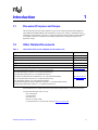
Introduction
1.1
Document Purpose and Scope
This document describes the Intel® IQ80333 I/O processor evaluation platform board (IQ80333)
using DDR-II 400 MHz SDRAM. The Intel®80333 I/O processor (80333) is intended for rapid,
intelligent I/O development. The 80333 is a multi-function device that integrates the Intel XScale®
core (ARM* architecture compliant) with intelligent peripherals including a PCI Express bus
application bridge.
1.2
Other Related Documents
Table 1.
Intel® 80333 I/O Processor Related Documentation List
Document
Intel®80333
Intel
® 80333
I/O Processor Developer’s Manual
305432
I/O Processor Datasheet
305433
Intel®80333 I/O Processor Design Guide
Intel
® 80333
Number
I/O Processor Specification Update
®
Intel Flash Recovery Utility (FRU) Reference Manual
IEEE Standard Test Access Port and Boundary-Scan Architecture (IEEE JTAG-1149.1-1990)
305434
305435
274071
http://www.ieee.org
PCI Local Bus Specification, Revision 2.3 - PCI Special Interest Group
PCI Express Specification, Revision 1.0a - PCI Special Interest Group
PCI Express Base Specification 1.0a - PCI Special Interest Group
PCI Express Card Electromechanical Specification 1.0a - PCI Special Interest Group
PCI Local Bus Specification, Revision 2.3 - PCI Special Interest Group
http://www.pcisig.com
/specifications
PCI-X Specification, Revision 1.0b - PCI Special Interest Group
PCI Bus Power Management Interface Specification, Revision 1.1 - PCI Special Interest Group
PCI Bus Hot-Plug Specification, Revision 1.1 - PCI Special Interest Group
Intel documentation is available from the local Intel Sales Representative or Intel Literature Sales.
To obtain Intel literature write to or call:
Intel Corporation
Literature Sales
P.O. Box 5937
Denver, CO 80217-9808
(1-800-548-4725) or visit the Intel website at http://www.intel.com
Customer Reference Board Manual
9
Intel® IQ80333 I/O Processor
Introduction
1.3
Electronic Information
Table 2.
Electronic Information
Support Type
Location/Contact
The Intel World-Wide Web (WWW) Location:
http://www.intel.com
Customer Support (US and Canada):
1.4
1-916-377-7000
Component References
Table 3 provides additional information on the major components of 80333.
Table 3.
Component Reference
Component
Part Number
Intel
StrataFlash®
Memory
28F640J3C
Intel(R)
Gigabit
Ethernet
Controller
82545EM
Additional Information
•
Manufacturer: Intel Corporation
• URL: http://developer.intel.com/design/flcomp/prodbref/298044.htm
• Manufacturer: Intel Corporation
• URL: http://developer.intel.com/design/network/products/lan/controllers/82545.htm
•
Manufacturer: Grayhill*
• URL:
http://embrace.grayhill.com/embrace/Item/ASP/Item-Detail.asp?PartNo=94HAB16W&Catalog
GroupID=Series94HBinaryCoded&GroupDisplayLabel=&RestSes=No
Rotary Switch
DR FC 16
Hex Display
HDSP-A103
AudioBuzzer
DMT 1206
SMT
NVSRAM
STK14C88-3
N 35
• Manufacturer: SIMTEK*
CPLD
XC9572XL 10TQ100C
• Manufacturer: XILINK*
•
Manufacturer: Agilent Technologies*
• URL: http://www.semiconductor.agilent.com/cgi-bin/morpheus/home/home.jsp?pSection=LED
•
Manufacturer: RDI*
• URL: http://www.rdi-electronics.com/products/Audio/DMT-1206-SMT.html
• URL: http://www.simtek.com/product-information/datasheets/256K-PDF/STK14C88-3.pdf
• URL: http://www.xilinx.com/bvdocs/publications/ds057.pdf
• Manufacturer: National*
Temperature
Sensor
LM75CIMX-3
Programmable Reset
IC
MAX6306UK
29D3
• Manufacturer: Maxim*
Registered
Buffer
IDT74SSTU3
2864BF
• Manufacturer: IDT* (Integrated Device Technology)
Programmable PLL
IDTCSPU877
BV
• Manufacturer: IDT* (Integrated Device Technology
256 bit 1-wire DS2430A_TS
EEPROM
OC
3.3V
Transceiver
MAX561
Battery
Charger
ADP3801
10
• URL: http://www.national.com/pf/LM/LM75.html
• URL: http://www.maxim-ic.com/quick_view2.cfm/qv_pk/1524
• URL: http://www1.idt.com/pcms/products.taf?catID=97&genID=74SSTU32864
• URL: http://www1.idt.com/pcms/products.taf?catID=112&genID=CSPU877
• Manufacturer: Maxim*
• URL: http://www.maxim-ic.com/quick_view2.cfm?qv_pk=2913
• Manufacturer: Maxim*
• URL: http://www.maxim-ic.com/quick_view2.cfm?qv_pk=1544
• Manufacturer: Analog Devices*
• URL: http://www.analog.com/UploadedFiles/Data_Sheets/308746738ADP3801_2_0.pdf
Customer Reference Board Manual
Intel® IQ80333 I/O Processor
Introduction
1.5
Terms and Definitions
Table 4.
Terms and Definitions
Acronym/Term
Definition
ARM
Refers to both the microprocessor architecture and the company that licenses it.
CRB
Customer Reference Board
ICE
In-Circuit Emulator – A piece of hardware used to mimic all the functions of a
microprocessor.
IOP
I/O processor
JTAG
Joint Test Action Group – A hardware port supplied on Intel XScale® microarchitecture
evaluation boards used for in-depth testing and debugging.
PPCI-X
Primary PCI-X.
PSU
Power Supply Unit
SPCI-X
Secondary PCI-X.
Customer Reference Board Manual
11
Intel® IQ80333 I/O Processor
Introduction
1.6
Intel® 80333 I/O Processor
The 80333 is a follow-on product to the Intel® 80332 I/O processor (80332). It is a multi-function
device that combines the Intel XScale® core with intelligent peripherals, and integrates two
PCI Express to PCI-X Bridges. The 80333 consolidates into a single system:
•
•
•
•
•
Intel XScale® core with an internal bus operating at 333 MHz.
•
•
•
•
•
•
•
•
High-Performance Memory Controller.
x8 PCI Express Upstream Link.
Two PCI Express-to-PCI Bridges supporting PCI-X interface on both segments.
PCI Standard Hot Plug Controller (segment B).
Address Translation Unit (ATU): PCI-to-Internal Bus Application Bridge, interfaced to the
segment A.
Interrupt Controller with 17 external interrupt inputs.
Two Direct Memory Access (DMA) Controller.
Peripheral Bus Interface (PBI) Unit.
Enhanced Application Accelerator Unit (AAU) which supports RAID 6 functionality.
Two I 2C Bus Interface Units (BIU).
Two 16550 Compatible UARTs with flow control (4 pins).
Eight General Purpose Input Output (GPIO) Ports.
The 80333 is an integrated processor that addresses the needs of intelligent I/O applications and helps
reduce intelligent I/O system costs.
PCI Express is an industry standard, high performance, low latency system interconnect. The 80333
PCI Express upstream link is capable of x8 lane widths at 2.5 GHz operation as defined by the PCI
Express Specification, Revision 1.0a. The addition of the Intel XScale® core brings intelligence to the
PCI Express-to-PCI Bridges.
The 80333 integrates dual PCI Express-to-PCI-X Bridges with the ATU as an integrated secondary
PCI device. The Upstream PCI Express port implements the PCI-to-PCI Bridge programming model
according to the PCI Express Specification, Revision 1.0. The Primary Address Translation Unit is
compliant with the PCI-X Addendum to the PCI Local Bus Specification, Revision 1.0a definitions of
an ‘application bridge’.
For more in depth information in regards to the 80333, please see the Intel®80333 I/O Processor
Developer’s Manual.
12
Customer Reference Board Manual
Intel® IQ80333 I/O Processor
Introduction
Figure 1.
Intel® 80333 I/O Processor Block Diagram
!
"
#$ (!/
0 (%%
(
- & ) "*+,
%
&'
.
"(
/#
(/ "
3
(
" '(
#
"3
'(
1
23
( ' ) "*+,
(
*
1
23
) "*+,
Customer Reference Board Manual
13
Intel® IQ80333 I/O Processor
Introduction
1.7
Intel® IQ80333 I/O Processor Evaluation Platform
Board Features
Table 5.
Summary of Features
Feature
Definition
Battery Backup Unit: Battery back up circuit for SDRAM.
Ethernet
Intel(R) 82545EM Gigabit Ethernet Controller
Flash ROM: 8 MB Flash ROM 3.3 V – 16-bit Flash I/F.
Form Factor:
PCI-Express card (312 X 107 mm)
General Purpose I/O: GPIO Pins are used as described in the appropriate section in this document
Hex Display:
JTAG Port:
Logic Analyzer:
Two 7-segment Hex LED displays.
ARM compliant JTAG Header.
Logic analyzer connectors on the DDRII SDRAM interface.
Interposer Card may be used for the memory bus – Information supplied separately.
• 256 MB (512 Mb x 16) DDRII SDRAM 400 MHz DIMM.
Memory:
• ECC
• Registered
Board sources +1.25 V, +2.5 V, +3.3 V, +5 V, +12 V, and -12 V from primary PCI
connector.
Onboard Power:
• All core voltages are derived from 3.3 V supply.
• Auxiliary power for the Secondary PCI slot.
Power LED: Power on (green).
Primary PCI: PCI Express - x8 lane
RAID Support
Support for “RAID” 6 functionality– Ability to make the devices plugged in the
secondary expansion slots “Private”.
Integrated XOR engine and two iSCSI CRC32C off-load engines.
• 1 64-bit PCI-X connector - 133 MHz.
Secondary PCI:
• 1 64 bit 100 MHz PCI-X
• Intel(R) 82545EM Gigabit Ethernet Controller also on the 100 MHz PCI.
Serial Port:
14
Dual RJ11 serial port connectors. The 80333 has two integrated UART serial ports
which are 16550 compatible.
Customer Reference Board Manual
Getting Started
2
The 80333 is a software development environment for IQ80333. Software updates and additional
offerings from vendors can change frequently. To keep up-to-date, please visit
http://www.intel-ioprocessortools.com/kshowcase/view for the latest updates.
2.1
Kit Content
The 80333 Kit contains the following items:
•
•
•
•
2.2
IQ80333 with 400 MHz DDRII SDRAM DIMMs
Code|Lab* Development Environment from Accelerated Technology Incorporated*
JTAG Emulation unit
Serial Cable and RJ11 Adapter
Hardware Installation
Warning:
2.2.1
Static charges can severely damage the boards. Be sure you are properly grounded before removing
the board from the anti-static bag.
First-Time Installation and Test
For first-time installation, visually inspect the 80333 for any damage made during shipment. Follow
the host system manufacturer’s instructions for installing a PCI Express adapter card. The board is a
full-length host bus adapter card that requires a PCI Express slot free from obstructions. The IQ80333
has a x8 (read as ‘by eight’) edge connector.
Note:
Please note, at this time the IQ80333 does NOT work in a passive backplane. This is due to the
nature of the PCI Express linking protocol. For the I/O processor to successfully come out of reset,
a link must be established on the PCI Express bus. Without another device on a passive backplane
to ‘talk to’, a link is not established.
Customer Reference Board Manual
15
Intel® IQ80333 I/O Processor
Getting Started
2.2.2
Power Requirements
The 80333 requires a 3.3 V supply coming through the PCI Express primary connector. Plug the
board into a desktop with a PCI Express slot.
The 80333 has an auxiliary power receptacle (J1A1, see Section 3.9.4, “Connector Summary”) that
is used to power the secondary PCI-X slot. This connector is compatible with a standard ATX hard
drive power connector.
Caution:
16
Before connecting power to the entire system, verify that the auxiliary system power to the
secondary PCI-X slot and the main power to the 80333 are both connected. Both power rails should
come up at the same time. When there is not a card plugged into the secondary PCI-X slot, then the
auxiliary power can be left unconnected.
Customer Reference Board Manual
Intel® IQ80333 I/O Processor
Getting Started
2.3
Factory Settings
Make sure that the switch/jumper settings are set to proper positions as explained in Section 3.9,
“Switches and Jumpers” on page 38.
2.4
Development Strategy
2.4.1
Supported Tool Buckets
For developing and debugging software application, the production version of the 80333 kit includes
the Code|Lab Development Environment. Support for the Code|Lab development environment is
available from MGC*. Please refer to the enclosed package.
The following tools are available for evaluation purposes (please contact appropriate vendor). These
tools are for evaluation purposes and do not include any support. Please contact the vendor directly
for additional information and support. They include, but are not limited to:
•
•
•
•
•
•
RedHat* GNUPro tools
ARM RealView Developer Suite
WindRiver* VxWorks* RTOS and Tornado* Development Tools
Wasabi Systems NetBSD* OS
TimeSys* Linux* RTOS
Accelerated Technology Inc.*, Nucleus Plus* RTOS and Development Tools
Please contact your Intel representative for the latest updates or visit
http://www.intel-ioprocessortools.com/kshowcase/view.
2.4.2
Contents of the Flash
The production version of the board contains an image for RedHat RedBoot* target monitor.
Customer Reference Board Manual
17
Intel® IQ80333 I/O Processor
Getting Started
2.5
Target Monitors
2.5.1
RedHat RedBoot
RedBoot* is an acronym for “RedHat Embedded Debug and Bootstrap”, and is the standard
embedded system debug/bootstrap environment from RedHat, replacing the previous generation of
debug firmware: CygMon and GDB stubs. It provides a bootstrap environment for a range of
embedded operating systems, such as embedded Linux and eCos*, and includes facilities such as
network downloading and debugging. It also provides a simple Flash file system for boot images.
RedBoot provides a set of tools for downloading and executing programs on embedded target
systems, as well as tools for manipulating the target system's environment. It can be used for both
product development (debug support) and for end product deployment (Flash and network booting).
Here are some highlights of RedBoot capabilities:
• Boot scripting support
• Simple command line interface for RedBoot configuration and management, accessible via
serial (terminal) or Ethernet (telnet) (see Section 2.6.4, “GNUPro GDB/Insight” on page 21)
• Integrated GDB stubs for connection to a host-based debugger (GBD/Insight) via serial or
Ethernet. (Ethernet connectivity is limited to local network only)
• Attribute Configuration - user control of aspects such as system time and date (when
applicable), default Flash image to boot from, default fail-safe image, static IP address, etc.
•
•
•
•
18
Configurable and extensible, specifically adapted to the target environment
Network bootstrap support including setup and download, via BOOTP, DHCP and TFTP
X/Y-Modem support for image download via serial
Power On Self Test
Customer Reference Board Manual
Intel® IQ80333 I/O Processor
Getting Started
2.6
Host Communications Examples
How to communicate to the host.
2.6.1
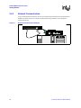
Serial-UART Communication
Using a serial connection to communicate with the board (Figure 2). Please note that the evlaution
board is plugged into a host machine, as in the figure below. You can use an additional laptop
computer, but it is not necessary. The host computer, when loaded with the proper software can
communicate with the board.
Figure 2.
Serial-UART Communication
Laptop computer
2.6.2
JTAG Debug Communication
Using a JTAG Emulator to communicate with the board (Figure 3). Please note that the evaluation
board is plugged into a host machine, as in the figure below. You can use an additional laptop
computer, but it is not necessary. The host computer, when loaded with the proper software can
communicate with the board.
Figure 3.
JTAG Debug Communication
Laptop computer
Customer Reference Board Manual
19
Intel® IQ80333 I/O Processor
Getting Started
2.6.3
Network Communication
Using a standard network connection, the user can communicate with the board via the ethernet port.
Redboot also allows the user to remotely boot the platform using a BOOTP server through the
network Connection.
Figure 4.
Network Communication Example
A
B
C
D
E
F
G
H
S EL EC T E D
O N -L IN E
20
Customer Reference Board Manual
Intel® IQ80333 I/O Processor
Getting Started
2.6.4
GNUPro GDB/Insight
2.6.4.1
Communicating with RedBoot
Hardware Setup:
• Host with UNIX/Linux or Win32 installed
• IQ80333 with serial cable
• RedHat RedBoot monitor Flashed to the platform board
Recommended Mapping of UART Ports to Host Com Ports
• Host port connected to the platform board UART.
The following communication tools can be used:
•
•
•
•
Win32 using HyperTerminal
UNIX using Kermit
Linux using Minicom
Solaris using Tip
RedBoot Monitor startup:
Description: terminal emulator runs on host and communicates with the board via the serial cable.
Start:
Power up the IQ80333. While the 'reset' is asserted, the two 7-segment LEDs
sequentially display “88”, “A0” through “A6”, followed by “SL” (Scrub loop). When
RedBoot is successfully booted, it displays the characters “A1” on the LEDs. When
the final state of “A1” does not occur, reset the processor again.
The time for reset is approximately 1 or 2 seconds.
Win32 on Host Connecting with HyperTerminal.
Customer Reference Board Manual
21
Intel® IQ80333 I/O Processor
Getting Started
To bring up a HyperTerminal session on a Win32 platform: Go to Start, Programs, Accessories,
Communications, HyperTerminal
• HyperTerminal setup screens:
— “Connection Description” Panel:
• Enter name.
— “Connect To” Panel:
• Select host com2 port (or whichever port you are using).
— Port Settings:
• Bits per second: 115200
• Data Bits: 8
• Parity: none
• Stop Bits: 1
• Flow Control: none
— Start HyperTerminal:
• Select Call from HyperTerminal panel.
— Reset or power up IQ80333.
— The Host screen reads:
RedBoot(tm) debug environment - built dd:mm:yy, Mon dd 2004
Platform: 80333
Copyright (C) 2004, RedHat, Inc.
RAM: 0xa0000000-0xa2000000
FLASH: 0x00000000 - 0x00800000, 64 blocks of 0x00020000 bytes each.
IP: 192.168.0.1, Default server: 0.0.0.0
RedBoot>
For further information on the GDB/Insight Debugger, refer to the content of the GNUPro CD and/or
the GNUPro Debugging Tools manual. This setup assumes that RedBoot is Flashed on the board.
22
Customer Reference Board Manual
Intel® IQ80333 I/O Processor
Getting Started
2.6.4.2
Connecting with GDB
Below are the GDB commands entered from the command prompt. Be sure system path is set to
access “xscale-elf-gdb.exe”. File name in example “hello”. Bold type represents input by user:
>xscale-elf-gdb -nw hello1
• Start GDB executable, loads debug information and symbols.
(GDB) set remotebaud 115200
• Set baud rate for the 80333.
Connect COM port:
• When using Windows command prompt:
(GDB) target remote com1
Example: screen output from board to host (GDB) target remote com1:
Remote debugging using com1.
(GDB)
• When using Linux
(GDB) target remote /dev/ttyS0
(GDB) load
• Load the program to the board, may have to wait a few seconds.
(GDB) break main
• Set breakpoint at main.
(GDB) continue
• Start the program using 'continue' verse the usual 'run'.
• Program hits break at main() and wait.
1.
To be supplied separately.
Customer Reference Board Manual
23
Intel® IQ80333 I/O Processor
Getting Started
This Page Left Intentionally Blank
24
Customer Reference Board Manual
Intel® IQ80333 I/O Processor
Hardware Reference Section
3
Hardware Reference Section
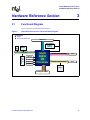
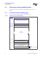
3.1
Functional Diagram
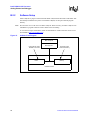
Figure 5 shows the functional block for the 80333.
Figure 5.
Intel® 80333 I/O Processor Functional Block Diagram
Target Market
ROMB
PCI Express RAID card
DDR II 400
HEX
LED
DDR SDRAM
Battery
Backup
Buzzer
Local Bus
I2C
GPIOs
JTAG
PCI
Express
8 MB
StrataFLASH
RS-232
RS-232
Intel®
80333
I/O
Processor
PCI-X Bus Slot (133 MHz)
Slot
PCI-X Bus IOP (100 MHz)
Slot
Gig-E
X8 Edge Connector
Customer Reference Board Manual
25
Intel® IQ80333 I/O Processor
Hardware Reference Section
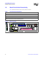
3.2
Board Form-Factor/Connectivity
Table 6 summarizes the form-factor and connectivity features for the 80333.
Table 6.
Form-Factor/Connectivity Features
Description
The IQ80333 is a x8 PCI Express card with form factor depicted by Figure 6.
The 80333 connects to the Primary PCI-Express bus of the host machine.
The 80333 has two PCI-X expansion slot.
The 80333 has two serial ports and one RJ-45 Ethernet port.
The 80333 has one JTAG port compliant with ARM Multi-ICE 20-pin connector standard. The JTAG is targeted for the Intel
XScale® core and the CPLD, and is used for software debug purposes.
Board Form Factor
P C I -X S lo t
JTAG
A ux
P ow er
82545 EM
G bE
( s tr a d d le s b o a r d e d g e )
I2C
Figure 6.
P e rip h e ra l B u s H e a d e r
P o w e r S ta tus
D D R I I D IM M
C P LD
F la s h
R J -1 1
S e r ia l p o rts
Buffer
107
B uz
zer
D IP S w itc h
S e ria l
R J -4 5 E E P R O M
E th e r n e
t
In te l®
80333
I/O
P ro c e s s o r
R o ta ry
S w itc h
In tr /G P IO
H ea der
B a t te ry
P C I- X R t A n g le S lo t
(M o u n te d o n B a c k S id e o f P C B )
P C I- E
Edge
312
26
Customer Reference Board Manual
3.3
Power
The 80333 draws power from the PCI Express bus. The power requirements for the 80333 are shown
in Table 7 below. The numbers do not include the power required by a PCI-X card mounted on the
expansion slot.
Table 7.
Note:
Power Features
Voltage Rail
Maximum Current
+3.3 V
6971 mA
+5 V
7 mA
+12 V
105 mA
The maximum current was calculated, but not measured. This numbers do not include the power
required by a PCI-X card mounted on the expansion slot(s).
Customer Reference Board Manual
27
Intel® IQ80333 I/O Processor
Hardware Reference Section
3.4
Memory Subsystem
The Memory Controller of 80333 controls the DDR SDRAM memory subsystem. It features programmable chip selects and support for error correction codes (ECC). The memory controller can
be configured for DDR SDRAM at 333 MHz and DDR-II at 400 MHz. The memory controller
supports pipelined access and arbitration control to maximize performance. The memory controller
interface configuration support includes Unbuffered DIMMs, Registered DIMMs, and discrete
DDR SDRAM devices.
This IQ80333 has DDR-II at 400 MHz DIMM on the board. The memory subsystem of the
evaluation board consists of the SDRAM as well as the Flash memory subsystems.
3.4.1
DDR SDRAM
The DDR SDRAM interface consists of a 64-bit wide data path to support up to 3.2 Gbytes/sec
throughput. An 8-bit Error Correction Code (ECC) is stored into the DDRII SDRAM array along
with the data and is checked when the data is read.
The IQ80333 features on board registered DDRII 400 MHz SDRAM, arranged 512 Mbit x16 in
density (256 MB), and with ECC.
3.4.1.1
Battery Backup
Battery backup is provided to save any information in DDR during a power failure. The evaluation
board contains a 4 V Li-ion battery, a charging circuit and a regulator circuit.
DDRII technology provides enabling data preservation through the self-refresh command. When the
processor receives an active Primary PCI-X reset, the self-refresh command issues, driving SCKE
signals low. Upon seeing this condition, the board logic circuit holds SCKE low before the processor
loses power. Batteries maintain power to DDRII and logic, to ensure self-refresh mode. When the
circuit detects PRST# returning to inactive state, the circuit releases the hold on SCKE. Removing the
battery can disable the battery circuit. When the battery remains in the platform when it is de-powered
and/or removed from the chassis, the battery maintains DDRII for about four hours. Once power is
reapplied, the battery is fully charged.
The CPLD contains information in regards to the battery status. Please see Section 3.6.7, “Battery
Status” on page 34 for more details.
28
Customer Reference Board Manual
Intel® IQ80333 I/O Processor
Hardware Reference Section
3.4.2
Flash Memory Requirements
Total Flash memory size is 8 MB.
Table 8.
Flash Memory Requirements
Description
IQ80333 Total Flash size is 8 MB
80333 Flash technology is based on Intel StrataFlash® family
80333 Flash uses a 16-bit interface
80333 Flash utilizes the 80333 Peripheral Bus
80333 May be programmed using the PCI-X interface – Flash Recovery Utility (FRU) Utility
80333 May be programmed using a RAM based software target monitor – RedHat RedBoot and ARM Firmware Suite
80333 May be programmed using a JTAG emulation/debug device
Customer Reference Board Manual
29
Intel® IQ80333 I/O Processor
Hardware Reference Section
3.5
Interrupt Routing
The 80333 Interrupt routing.
Table 9.
30
External Interrupt Routing to Intel® 80333 I/O Processor
Interrupt
System Resource
HPI#
Temperature Sensor, Header
S_INTA#
PCI-X Slot INTB#, Header
S_INTB#
PCI-X Slot INTC#, Header
S_INTC#
PCI-X Slot INTD#, Header
S_INTD#
PCI-X Slot INTA#, Header
P_INTA#
PCI-X Card Edge INTA#, Header
P_INTB#
PCI-X Card Edge INTB#, Header
P_INTC#
PCI-X Card Edge INTC#, Header
P_INTD#
PCI-X Card Edge INTD#, Header
Customer Reference Board Manual
Intel® IQ80333 I/O Processor
Hardware Reference Section
3.6
Intel® IQ80333 I/O Processor Evaluation Platform
Board Peripheral Bus
The 80333 populates the peripheral bus as depicted by Figure 7.
Figure 7.
Intel® IQ80333 I/O Processor Evaluation Platform Board Peripheral Bus Topology
Intel® 80333
I/O Processor PBI Bus
PC 104
Connector
Agilent*
HDSP-A103 Hex
Display
FLASH 28F640J3C
16-bit
8 Mb
RDI
DMT-1206-SMT
Audio Buzzer
Grayhill
HAB16W
Rotary Switch
XILINX
XC9572XL10TQ100C
CPLD
SIMTEK
STK14C88-3 N 35
NVSRAM
The devices on the bus include Flash ROM, audio buzzer, CPLD, HEX display, NVSRAM, and
rotary switch.
Table 10.
Peripheral Bus Features
Description
The bus width can be 8-bit or 16-bit and runs at 66 MHz.
The bus is utilized for attaching debug and Flash devices.
The interfaces/devices that are utilized include an audio buzzer, CPLD, a rotary switch, a HEX Display, and
NVSRAM.
Customer Reference Board Manual
31
Intel® IQ80333 I/O Processor
Hardware Reference Section
3.6.1
Flash ROM
Table 11.
Flash ROM Features
Description
Flash is an Intel
StrataFlash®
technology – Part number: 28F640J3C
Flash size is 8 MB
The connection to the peripheral bus is depicted by Figure 8
Flash Connection on Peripheral Bus
Intel® 80333
I/O Processor
Flash
28F640J3C
16-bit
8 Mb
CS
PCE0
Figure 8.
Intel® 80333 I/O Processor
32
Customer Reference Board Manual
Intel® IQ80333 I/O Processor
Hardware Reference Section
3.6.2
UART
The 80333 has two integrated UARTs. Each asynchronous serial ports supports all the functions of a
16550 UART. The UART signals are connected to a dual RS-232 buffer and then to a RJ-11 serial
port connector mounted on the bracket of the evaluation board. The serial port and GPIO signals are
muxed on the same pins. Jumper J1D2, located next to the serial port buffer can disable the buffer to
allow the signals to be used as GPIO signals. Please see Section 3.9.3, “Jumper Summary” on
page 39 for more details.
3.6.3
Non-Volatile RAM
In addition to the 8MB Flash device, the IQ80333 has a separate 32 K by 8 non-volatile RAM device
on the peripheral bus. The NVRAMs address range is from CE87 0000 to CE87 FFFF (in hex).
Please see Section 4.2.2, “Peripheral Bus Memory Map” on page 47 for more details.
3.6.4
Audio Buzzer
The 80333 evaluation board has an audio buzzer that is turned on and off by writing to the Buzzer
Control Register located in the CPLD. Jumper J9D3 adjusts the volume from off, to soft, to loud.
Please see Section 3.9.3, “Jumper Summary” on page 39 for more details. The audio buzzer’s
address range is from CE86 0000 to CE86 FFFF (in hex). Please see Section 4.2.2, “Peripheral Bus
Memory Map” on page 47 for more details.
3.6.5
HEX Display
The two pairs of Agilent HDSP-A103 seven segment LEDs are used for displaying POST codes or
other software generated debug codes. Both HEX displays are individually addressed. The left HEX
display address range is CE84 0000 to CE84 FFFF (in hex). The right HEX display address range is
CE85 0000 to CE85 FFFF (in hex). Please see Section 4.2.2, “Peripheral Bus Memory Map” on
page 47 for more details.
3.6.6
Rotary Switch
The 80333 provides a Rotary Switch (S8A1) for the user to select from different boot-up flavors.
Setting ‘0’ enables private devices on the secondary PCI-X bus. Setting ‘0’ allows Redboot to
configure and use devices in slot A. Position ‘1’ allows the host to see all the devices on the
secondary PCI bus. The default setting is position 0. Other settings are currently not validated with
Redboot. Other settings may be used with other software applications. Please see Section 4.2.2,
“Peripheral Bus Memory Map” on page 47 for more details on addressing the rotary switch.
Table 12.
Rotary Switch Requirements
Description
Rotary switch has a 4-bit resolution (16 positions).
The connection to the peripheral bus is depicted by Figure 7.
Default setting is ‘0’. This enables private devices on PCI-X bus.
Position ‘1’ allows host to see all devices on the secondary bus.
Customer Reference Board Manual
33
Intel® IQ80333 I/O Processor
Hardware Reference Section
3.6.7
Battery Status
A CPLD on the IQ80333 provides the following status for the battery. Please see Section
4.2.2, “Peripheral
Bus Memory Map” on page 47 for more details on addressing the CPLD.
Table 13.
34
Battery Status Buffer Requirements
BIT
Read/
Write
0
R
Battery Present
1
R
Battery Charged
2
R
Battery Discharged
3
R/W
4-7
*
Name
Battery Enable
Reserved
Description
• 0 = No backup battery
• 1 = Battery backup is present
• 0 = Battery is not fully charged
• 1 = Battery is fully charged
• 0 = Battery backup is not fully discharged
• 1 = Battery backup is fully discharged
• 0 = Disable battery backup
• 1 = Enable battery backup
Undefined
Customer Reference Board Manual
Intel® IQ80333 I/O Processor
Hardware Reference Section
3.7
Debug Interface
3.7.1
Console Serial Port
The platform has two serial ports for debug purposes as described in Section 3.6, “Intel® IQ80333
I/O Processor Evaluation Platform Board Peripheral Bus” on page 31.
Customer Reference Board Manual
35
Intel® IQ80333 I/O Processor
Hardware Reference Section
3.7.2
JTAG Debug
The 80333 has a 20-pin JTAG connector (J7D2) that is in compliant with ARM Multi-ICE guidelines.
3.7.2.1
JTAG Port
Figure 9.
JTAG Port Pin-out
VTref
1
2
Vsupply
nTRST
3
4
GND
TDI
5
6
GND
TMS
7
8
GND
TCK
9
10
GND
RTCK
11
12
GND
TDO
13
14
GND
nSRST
15
16
GND
DBGRQ
17
18
GND
DBGACK
19
20
GND
A9457-01
36
Customer Reference Board Manual
Intel® IQ80333 I/O Processor
Hardware Reference Section
3.8
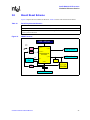
Board Reset Scheme
Figure 10 depicts the reset scheme for the 80333. Table 14 list the reset schemes for the 80333.
Table 14.
Reset Requirements/Schemes
Description
Primary PCI reset, resets all devices on the board. It occurs during the power-up.
The SRST signal from the JTAG connector is a bi-directional signal that can force a reset similar to the
power-up reset on the board.
Figure 10.
RESET Sources
DDR II SDRAM
Reset
Button
M_RST#
RESETIN
#
Debounce
Power
Delay
PCI-X Con B
B_RST#
PWRDELAY
Intel® 80333 I/O
Processor
PCI-X Con A
A_RST#
JTAG
Con
TRST
#
SRST
#
TRST
#
CPLD
PWRGD
RST#
LAN_PWR_GOOD
Voltage
Monitor
Isolation
82545EM
Pwrgood
PCI-E Con
Customer Reference Board Manual
37
Intel® IQ80333 I/O Processor
Hardware Reference Section
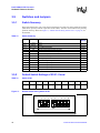
3.9
Switches and Jumpers
3.9.1
Switch Summary
Please note that the term ‘open’ refers to the individual pin of switch S7A1 being pushed in at bottom
(small dot on pin away from the ‘open’ label on the switch). The term ‘closed’ refers to the pin being
pushed in at the top. Please see Figure 11, “Default Switch Setting Switch S7A1” on page 38, for
more details.
Table 15.
Switch Summary
Switch
S1C1
S6A1
Association
Factory
Default
Description
80333
Reset
BPCI-X
Reset
S7A1-1
APCI-X Bus
S7A1-2
IOP
RESET: Sets IOP Reset-Mode operation
PCI-XBus A Speed Set
Closed
Open
S7A1-3
IOP
RETRY: Sets IOP RETRY-Mode operation
Open
S7A1-4
BPCI-X Bus
PCI-X Bus B speed set
Closed
S7A1-5
BPCI-X Bus
PCI-X Bus B Hot Plug Reset
Closed
Closed
S7A1-6
BPCI-X Bus
Hot Plug Capable Disable
S7A1-7
SMBUS Bus
SMBUS Manageability address bit 5
Open
S7A1-8
SMBUS Bus
SMBUS Manageability address bit 3
Open
S7A1-9
SMBUS Bus
SMBUS Manageability address bit 2
Open
S7A1-10
SMBUS Bus
SMBUS Manageability address bit 1
S8A1
CPLD
Open
Rotary Switch
Position 1
3.9.2
Default Switch Settings of S7A1- Visual
Table 16.
Switch S7A1
Figure 11.
Closed
Open
Open
Closed
Closed
Closed
Open
Open
Open
Open
S7A1
S7A1
S7A1
S7A1
S7A1
S7A1
S7A1
S7A1
S7A1
S7A1
1
2
3
4
5
6
7
8
9
10
Default Switch Setting Switch S7A1
1
2
3
4
5
6
7
8
9
10
Open
38
Customer Reference Board Manual
Intel® IQ80333 I/O Processor
Hardware Reference Section
3.9.3
Jumper Summary
Table 17.
Jumper Summary
Jumper
Description
J1C1
JTAG Chain Enable
J1D2
Disables UART
J7B4
SM_SCLK to EEPROM, SM_SDTA to EEPROM
1-2
Open
1-2, 3-4
J7D1
16-bit Flash Enable
Open
J9D3
Buzzer Volume
Open
3.9.4
Connector Summary
Table 18.
Connector Summary
Connector
Description
J1D1
RJ45 Network Connector for GbE NIC.
J1E1
RJ11 Dual Serial Port Connector.
J1L1, J1M1,
J1M2, J1N1,
J2M1, J2M2
SMA connectors
J1R1
Secondary PCI-X Expansion bus Slot
J2A1
Secondary PCI-X Expansion bus Slot.
J2D1
Power header for fan.
J2D2
GPIO tap-in Header
J1B1, J5D1,
J5C1
Test headers
J2E1
Edge connector for primary PCI Express Bus.
J5B1
DIMM
J7A1
PC104 Mod connector.
J7B1, J7B2
J7B3
3.9.5
Factory Default
I2C 4 pin connectors.
Secondary PCI-X Expansion Slot Power. Please see Section 2.2.2, “Power Requirements”
for more details
J7C1
Test header (empty)
J7D2
JTAG CPLD Header.
J9D1
Power header for battery.
General Purpose Input/Output Header
Table 19, “J2D2 GPIO Header Definition” on page 39 shows the GPIO signal assignments. The
GPIO signals are muxed with the serial port signals. The serial port must be disabled to use the GPIO
signals. These pins corespond to Jumper J2D2.
Table 19.
J2D2 GPIO Header Definition
Pin
Signal
Pin
Signal
Pin
Signal
1
GND
4
GPIO5
7
GPIO2
2
GPIO7
5
GPIO4
8
GPIO1
3
GPIO6
6
GPIO3
9
GPIO0
Customer Reference Board Manual
39
Intel® IQ80333 I/O Processor
Hardware Reference Section
3.9.6
Detail Descriptions of Switches/Jumpers
3.9.6.1
Switch S1C2: Intel® 80333 I/O Processor Reset
This switch resets 80333.
3.9.6.2
Switch S6A1: BPCI-X Reset
This switch resets the PCI-X B segment bus.
3.9.6.3
Switch S8A1: Rotary
Table 20.
Rotary Switch Settings
Position
Description
0
Enables private devices on the secondary PCI-X slot. Redboot uses this setting to configure
private devices
Factory Default
1
Disables private devices on the secondary PCI-X slot. This setting allows the host to see all
the devices on the secondary PCI bus.
2-F
These settings are meaningless to Redboot. Other applications may use these settings for
configuration or software utilization.
For more information, please see Section 3.6.6, “Rotary Switch” on page 33.
3.9.6.4
Switch S7A1
This 10 pin switch that allows the user to enable or disable various features. Please see specifics
below.
3.9.6.4.1
S7A1-1: PCI-X Bus A Speed Enable Corresponding to
Signal Name PBI_AD3
This switch allows the user to force the PCI-X bus A to run at 133 MHz or 100 MHz.
Table 21.
S7A1-1: PCI-X Bus A Speed Enable
S7A1-1
Open
Closed
3.9.6.4.2
Operation Mode
Enables 133 MHz on PCI-X bus A
Enables 100 MHz on PCI-X bus A (Default Mode)
S7A1-2: Reset I/O Processor Core Corresponding to
Signal Name PBI_AD5
RESET MODE is latched at the de-asserting edge of P_RST# and it determines when the 80333 is held
in reset until the Intel XScale® core Reset bit is cleared in the PCI Configuration and Status Register.
40
Customer Reference Board Manual
Intel® IQ80333 I/O Processor
Hardware Reference Section
Table 22.
Switch S7A1-2: Reset IOP: Settings and Operation Mode
S7A1-2
Open
Closed
3.9.6.4.3
Operation Mode
Don't hold in reset, enable IOP core (Default mode).
Hold IOP core in reset.
S7A1-3: Configration Cycle Enable Corresponding to
Signal Name PBI_AD6
Configuration Cycle Enable or RETRY is latched at the de-asserting edge of P_RST# and it
determines when the Primary PCI interface disable PCI configuration cycles by signaling a Retry
until the Configuration Cycle Retry bit is cleared in the PCI Configuration and Status Register.
Table 23.
Switch S7A1-3: RETRY: Settings and Operation Mode
S7A1-3
Open
Closed
3.9.6.4.4
Operation Mode
Configuration Retry Enabled. - use when booting in a host (Default mode).
Configuration Retry Disabled.
S7A1-4: PCI-X Bus B Speed Enable Corresponding to
Signal Name PBI_AD10
This switch allows the user to enables 133 MHz on PCI-X segment B.
Table 24.
S7A1-4: PCI-X Bus B Speed Enable: Settings and Operation Mode
S7A1-4
Open
Closed
3.9.6.4.5
Operation Mode
Enables 133 MHz on PCI-X bus B.
Enables 100 MHz on PCI-X bus B (Default Mode).
S7A1-5: PCI-X Bus B Hot-Plug Reset Disable
Corresponding to Signal Name PBI_AD11
This switch allows the user to enables or disable Hot-Plug Reset on PCI-X segment B.
Table 25.
S7A1-5: PCI-X Bus B Hot-Plug Reset Disable: Settings and Operation Mode
S7A1-5
Open
Closed
3.9.6.4.6
Operation Mode
PCI-X Bus B Hot-Plug Enable, normal reset mode disabled
PCI-X Bus B Hot-Plug Disable, normal reset mode (Default Mode).
Switch S7A1- 6: Hot Plug Capable Disabled Corresponding to
Signal Name PBI_AD15
This switch allows the user to enable hot plug devices on the secondary PCI-X bus B.
Table 26.
Switch S7A1- 6: Hot Plug Capable Disabled: Settings and Operation Mode
S7A1-6
Open
Closed
Operation Mode
Hot Plug on Bus B Enabled
Disables Hot Plug on Bus B(Default mode)
Customer Reference Board Manual
41
Intel® IQ80333 I/O Processor
Hardware Reference Section
3.9.6.4.7
Switch S7A1 - 7: SMBUS Manageability Address Bit 0
Corresponding to Signal Name PBI_AD17
This allows 80333 to address SMBus Slave Address bit 0 (PBI_A17).
Table 27.
Switch S7A1 - 7: SMBUS Manageability Address Bit 0: Settings and Operation Mode
S7A1-6
Open
Closed
3.9.6.4.8
Operation Mode
SMBus Manageablity Address Bit 0 = “1” (Default Mode)
SMBus Manageablity Address Bit 0 = “0”
Switch S7A1 - 8: SMBUS Manageability Address Bit 3
Corresponding to Signal Name PBI_AD18
This allows 80333 to address SMBus Slave Address bit 3 (PBI_A18).
Table 28.
Switch S7A1 - 8: SMBUS Manageability Address Bit 3: Settings and Operation Mode
S7A1-8
Open
Closed
3.9.6.4.9
Operation Mode
SMBus Manageablity Address Bit 3 = “1” (Default Mode)
SMBus Manageablity Address Bit 3 = “0”.
Switch S7A1- 9:SMBUS Manageability Address Bit 2
Corresponding to Signal Name PBI_AD17
This allows 80333 to address SMBus Slave Address2 (PBI_A17).
Table 29.
Switch S7A1 - 9: SMBUS Manageability Address Bit 2: Settings and Operation Mode
S7A1-9
Open
Closed
3.9.6.4.10
Operation Mode
SMBus Manageablity Address Bit 2 = “1” (Default Mode)
SMBus Manageablity Address Bit 2 = “0”.
Switch S7A1- 10: SMBUS Manageability Address Bit 1
Corresponding to Signal Name PBI_AD16
This allows 80333 to address SMBus Slave Address 1 (PBI_A16).
Table 30.
Switch S7A1 - 10: SMBUS Slave Address 0: Settings and Operation Mode
S7A1-10
Open
Closed
42
Operation Mode
SMBus Manageablity Address Bit 1 = “1” (Default Mode)
SMBus Manageablity Address Bit 1 = “0”.
Customer Reference Board Manual
Intel® IQ80333 I/O Processor
Hardware Reference Section
3.9.6.5
Jumper J7D1: Flash bit-width
Table 31.
The IQ80333 expects an 8-bit Flash enable.
Jumper J7D1: Descriptions
Jumper
J7D1
Table 32.
Description
8-bit Flash Enable
Open
Jumper J7D1: Settings and Operation Mode
Pins
Operation Mode
1-2
Enables 16-bit Flash
NC
8-bit Flash (default mode)
3.9.6.6
Jumper J1C1: JTAG Chain
Table 33.
Jumper J1C1: Descriptions
Jumper
J1C1
Table 34.
Description
Factory Default
JTAG Chain Enable
1-2
Jumper J1C1: Settings and Operation Mode
J1C1
Operation Mode
Pins 1, 2
Enables JTAG Chain for IOP only (Default Mode).
Pins 3, 4
Enables JTAG Chain for IOP + CPLD
Pins 5, 6
Enables JTAG Chain for IOP + CPLD + GBE
Pins 7, 8
Enables TRST# pull-down resistor
3.9.6.7
Jumper J1D2: UART Control
Table 35.
Jumper J1D2: Descriptions
Jumper
J1D2
Table 36.
Factory Default
Description
Factory Default
UART Control
Open
Jumper J1D2: Settings and Operation Mode
J1D2
Pins 1, 2
NC
Operation Mode
Disables UART/RS-232 port
Enables UART/RS-232 port (Default Mode)
Customer Reference Board Manual
43
Intel® IQ80333 I/O Processor
Hardware Reference Section
3.9.6.8
Jumper J7B4: SMBus Header
Table 37.
Jumper J7B4: Descriptions
Jumper
J7B4
Table 38.
Description
Factory Default
SMBus Header
1-2, 3-4
Jumper J7B4: Settings and Operation Mode
J7B4
Pins 1, 2
Operation Mode
Connects SM_SCLK to EEPROM U7B2 (Default Mode).
Pins 3, 4
Connects SM_SDTA to EEPROM U7B2 (Default Mode).
Pins 5, 6
Connects SM_SCLK to GE_SMCLK (for GBE control)
Pins 7, 8
Connects SM_SDTA to GE_SMDAT(for GBE control)r
Pins 9, 10
Connects SM_SCLK to PE_SMCLK (for PCI-E bus control)
Pins 11, 12
Connects SM_SDTA to PE_SM_SDAT (for PCI-E bus control)
3.9.6.9
Jumper J9D3: Buzzer Volume Control
Table 39.
Jumper J9D3: Descriptions
Jumper
J9D3
Table 40.
Description
Buzzer Volume
Open
Jumper J9D3: Settings and Operation Mode
J9D3
44
Factory Default
Operation Mode
Pins 2, 3
Buzzer Volume Soft
Pins 1, 2
Buzzer Volume Loud.
NC
Buzzer Volume Off.
Customer Reference Board Manual
Intel® IQ80333 I/O Processor
Software Reference
Software Reference
4.1
4
DRAM
For DDR SDRAM Sizes and Configurations, see theIntel® 80333 I/O Processor Developer’s
Manual. This section also contains multiple examples of Address Register Programming.
See the Intel® 80333 I/O Processor Design Guide, section 8, table 34 for supported DDR333 and
DDR-II configurations.
For all registers relating to DRAM and other MCU related registers, see the Intel® 80333 I/O
Processor Developer’s Manual.
4.2
Components on the Peripheral Bus
The 80333 has a peripheral bus which contains the following peripheral devices:
•
•
•
•
•
Flash ROM
CPLD
Audio Buzzer
Rotary Switch
Hex Display
Peripheral memory-Mapped Register Locations and all registers associated with PBI or the Peripheral
Bus Interface Unit can be found in the Intel® 80333 I/O Processor Developer’s Manual.
Customer Reference Board Manual
45
Intel® IQ80333 I/O Processor
Software Reference
4.2.1
Flash ROM
The Flash ROM is an 8 MB Intel StrataFlash® (part# 28F640) that sits on the Peripheral Bus and is
accessed using PCE0.
Flash Connection to Peripheral Bus
Intel® 80333
I/O Processor
Flash
28F640J3C
16-bit
8 Mb
CS
PCE0
Figure 12.
Intel® 80333 I/O Processor
Under normal operation, the very first instruction access by the Intel XScale® core begins at location
0x0 on the 80333 Internal Bus. By default, address 0x0 is pointing to PCE0 where Flash is located.
Currently, the Intel Flash Recovery Utility (FRU) can be used with the IQ80333. Another alternative
to FRU would be to reprogram the Flash through JTAG or using Redboot commands, when Redboot
is currently loaded onto the board. For more information on using Redboot to program the Flash,
please see Redboot Manual.
46
Customer Reference Board Manual
Intel® IQ80333 I/O Processor
Software Reference
4.2.2
Peripheral Bus Memory Map
The Table 41 is the physical memory map of the devices on the 80333 Peripheral Bus:
Table 41.
Peripheral Bus Memory Map
Address Range (in Hex)
Size
Data Bus Width
Description
C000 0000 - C07F FFFF
8 MB
8-bit or 16-bit
Flash memory (re-mapped)
CE80 0000 -CE80 FFFF
64 KB
8-bit
Product Code
CE81 0000 -CE81 FFFF
64 KB
8-bit
Board Stepping
CE82 0000 -CE82 FFFF
64 KB
8-bit
CPLD Firmware Revision
CE83 0000 -CE83 FFFF
64 KB
8-bit
Discrete LEDs
CE84 0000 -CE84 FFFF
64 KB
8-bit
Hex Display Left
CE85 0000 -CE85 FFFF
64 KB
8-bit
Hex Display Right
CE86 0000 -CE86 FFFF
64 KB
8-bit
Buzzer Control
CE87 0000 -CE87 FFFF
64 KB
8-bit
32 KB NV RAM
CE8D 0000 -CE8D FFFF
64 KB
8-bit
Rotary Switch
CE8E 0000 -CE8E FFFF
64 KB
8-bit
ESN I/O
CE8F 0000 -CE8F FFFF
64 KB
8-bit
Battery Status
Customer Reference Board Manual
47
Intel® IQ80333 I/O Processor
Software Reference
4.3
Board Support Package (BSP) Examples
Examples provided in this section are based on the RedHat* RedBoot software running on the
IQ80333.
4.3.1
Intel® 80333 I/O Processor Memory Map
Figure 13 depicts the memory space for the 80333 (before RedBoot boots):
Figure 13.
Intel® 80333 I/O Processor Memory Map
ADDRESS
0000 0000H
Memoryless Boot Registers
0000 0040H
ATU Outbound Direct Addressing Window
8000 0000H
ATU Outbound Memory Translation Windows
8800 0000H
9000 0000H
9001 0000H
Code / Data External Memory
ATU Outbound I/O Translation Window
Code/Data
External Memory
FFFF E000H
Peripheral Memory-Mapped Registers
FFFF E900H
I/O Processor Reserved
FFFF FFFFH
48
Reserved
Address
Space
External Memory
Customer Reference Board Manual
Intel® IQ80333 I/O Processor
Software Reference
4.3.2
RedBoot* Intel® 80333 I/O Processor Memory Map
Virtual Address
4.3.3
Physical Address
Size
(MB)
Description
0x0000 0000
0x0000 0000
2048
SDRAM - 64-bit ECC
0x8000 0000
0x8000 0000
128
ATU Outbound Memory Translation Windows
0x8800 0000
*
128
Unused
0x9000 0000
0x9000 0000
1
ATU OUtbound I/O Translation Window.
0x9010 0000
*
255
Unused
0xA000 0000
0x0000 0000
512
SDRAM - 64 bit ECC Uncached
0xC000 0000
0xC000 0000
8
Flash (PCE0#)
0xC080 0000
*
224
Unused
0xCE80 0000
0xCE80 0000
1
PCE1# - Uncached
0xCE90 0000
*
23
Unused
0xD000 0000
*
512
Unused
0xF00 0000
0xF00 0000
1
Cache flush
0xF010 0000
*
254
Unused
0xFFF0 0000
0xFFF0 0000
1
PMMR - Intel®80333 I/O processor Memory Mapped
Registers. Please see Chapter 17 of the Intel® 80333 I/O
Processor Developer’s Manual for more details.
RedBoot Intel® 80333 I/O Processor Files
Attached in the kit, find a copy of the RedHat eCos for IQ80333 CD. Once the CD is installed, you
may find:
• The RedBoot initialization code source files from the following location:
From the installed directory:
..\RedHat\eCos\packages\hal\arm\xscale\iq80333\current\include
• The RedBoot binary image files (downloadable onto Flash) from the following location:
From the installed directory:
..\RedHat\eCos\loaders\iq80333
To access RedHat GNUPro tools including RedBoot binaries and source code, you may also go to the
following location on the Intel site:
• http://developer.intel.com/design/intelxscale/dev_tools/021022/index.htm
Customer Reference Board Manual
49
Intel® IQ80333 I/O Processor
Software Reference
4.3.4
RedBoot Intel® 80332 I/O Processor DDR
Memory Initialization Sequence
In order to set the correct ECC bits, a DDR memory system (DIMM or discrete components) must be
written to with a known value. This process requires 64-bit writes to the entire DDR memory intended
for use. The following explains the sequence for memory initialization by RedBoot on an 80333 board
with an ECC DIMM. It also includes an example for the scrub (ECC initialization) code.
Initialization Sequence:
1. Disable interrupts. (Technically they are disabled at reset, but for soft reset this is included.
2. Init PBIU (Peripheral Bus Interface Unit) chip selects.
3. Enable I cache.
4. Move Flash to 0xF0000000.
5. Set TTB and Enable MMU.
6. Read DIM for memory parameters.
7. Set Memory Parameters.
8. Delay.
9. Turn DDRAM on.
10. Delay.
11. Enable Data Cache.
12. Enable BTB.
13. Flush all.
14. Clear ECC error logs.
15. Battery Test.
16. Enable ECC.
17. Scrub loop: Write zeros to all memory locations
mov
mov
mov
mov
mov
mov
mov
mov
mov
r8,
r0,
r1,
r2,
r3,
r4,
r5,
r6,
r7,
r4
#-1
#-1
#-1
#-1
#-1
#-1
#-1
#-1
// save DRAM size
ldr
r11, = SDRAM_BASE
// scrub Loop
0:
stmia
subs
bne
50
r11!, {r0-r7}
r12, r12, #32
0
Customer Reference Board Manual
Intel® IQ80333 I/O Processor
IQ80321 and IQ80333 Comparisons
IQ80321 and IQ80333 Comparisons
A
This appendix provides a brief description for differences between IQ80333 and IQ80321.
Table 42.
Intel® IQ80321 Evaluation Platform Board and
Intel® IQ80333 I/O Processor Evaluation Platform Board Comparisons
Features
Intel® IQ80333 I/O Processor Evaluation
Platform Board
Intel® IQ80321 Evaluation Platform Board
I/O Processor
80333
Intel® 80321 I/O Processor
Core/Microprocessor
Technology
Intel XScale® microarchitecture
Intel XScale® microarchitecture
Memory Technology
DDRII 400 MHz SDRAM DIMM
PC1600 DDR SDRAM (100 MHz Clock)
Form Factor
PC board that attaches to a PC/Server/Backplane Extended PC board that attaches to a
by a PCI Express slot – Two PCI-X Expansion Slot PC/Server/Backplane – One PCI-X Expansion Slot
PC/Server/Backplane
Connection
PCI Express
Expansion Card Slot
One PCI-X 100 MHz/64-bits
One PCI-X 133 MHz/64-bit
PCI-X 133 MHz/64-Bits or
PCI 66 MHz/64 Bits
One PCI-X 133 MHz/64-bit
PCI-X to PCI-X Bridge integrated with the
IQ80333l
IBM PCI-X Bridge
Reference: IBM 133 PCI-X Bridge
http://www.chips.ibm.com/
Interrupt Routing
External interrupts are routed through the XINT
pins on the 80333. Please see Table 9 for more
details.
External interrupts are routed through the XINT
pins on the 80321. They include INTA, INTB form
PCI-X expansion slot, INTA from 82544 GBE, and
UART interrupt – Steering and Status registers are
in 80321 – see Intel® 80321 I/O Processor
Developer’s Manual
Timers
Internal to 80333 – Refer to Intel® 80333 I/O
Processor Developer’s Manual
Internal to the 80321 - please refer to the Intel®
80321 I/O Processor Developer’s Manual
Local/Peripheral Bus
2-bit/33-100MHz multiplexed bus with six
66 MHz multiplexed bus with two chip-enables,
chip-enables, Synch/Asynchronous (IQ80321
Synch/Asynchronous (80333 operates in 66 MHz
operates in 33 MHz Asynchronous mode) –
Asynchronous mode) – Refer to PBI section in
Refer to PBI section in the IIntel® 80321 I/O
Intel® 80333 I/O Processor Developer’s Manual
Processor Developer’s Manual.
Flash Memory
8-bit or 16-bit, 8 MB accessed through Peripheral
Bus with chip-enable 0 (PCE0)
16-bit, 8 MB accessed through Peripheral Bus
with chip-enable 0 (PCE0))
Serial Debug Port
Two UARTs integrated within the 80333.
One UART on the Peripheral bus – 16C550
device
Network Debug Port
Intel® 82545EM GbE on the 100 MHz PCI-X bus Intel® 82544 GbE on the PCI-X bus
Rotary Switch
Same
Same
LED HEX Display
Same
Same
JTAG
20-PIN ARM Compliant
PCI/PCI-X Bridge
Logic Analyzer Connection Through PCI-X or PCI Express
Customer Reference Board Manual
20-PIN ARM Compliant
Various Mictors
51
Intel® IQ80333 I/O Processor
IQ80321 and IQ80333 Comparisons
This Page Left Intentionally Blank
52
Customer Reference Board Manual
Intel® IQ80333 I/O Processor
Getting Started and Debugger
Getting Started and Debugger
B.1
B
Introduction
This appendix pertains to Code|Lab version 2.3 and later which uses Microsoft's Visual Studio .NET.
For Code|Lab version 2.2 and earlier, refer to appendix B.
For more detailed information on JTAG and the 80333, please see the Intel® 80333 I/O Processor
JTAG Support White Paper.
B.1.1
Purpose
The purpose of this appendix is to help the user setup and become familiar with the IQ80333 and
other related hardware and software. This appendix steps the user through an example program using:
• Code|Lab EDE
• Code|Lab EDE debugger
• Macraigor* Raven* JTAG
This programming also includes:
• software setup
• compiling
• linking
• debugging example code
The user tours the major features of the debugger and explores some of the basics of debugging. By
the end of this exercise, the user has been given a general understanding of the MGC* development
tools and can begin working on new applications.
B.1.2
Necessary Hardware and Software
This example uses the MGC Code|Lab plug-in for Microsoft* Visual Studio, the GNU* Pro compiler,
the Macraigor Raven JTAG connector, and the 80333.
B.1.3
Related Documents
Table 43.
Related Documents
Document Title
Intel®
80333 I/O Processor Developer’s Manual
Intel® 80200 Processor based on Intel® XScale™ Microarchitecture Developer’s Manual
®
Hot-Debug for Intel XScale
™
Core Debug White Paper
Document #
305432
273411
273539
ARM Assemblers Guide (http://www.arm.com/support/574FKU/$File/ADS_AssemblerGuide_B.pdf)
ADS Debug Target Guide (http://www.arm.com/support/574FWT/$File/ADS_DebugTargetGuide_D.pdf)
Code|Lab Debug for ARMa
a.
This document installs to C:\MGC\docs\codelab debug.pdf.
Many of these documents load as part of MGC Code|Lab install (Start/Programs/ Accelerated
Technology/Documentation). This menu contains both the ARM* ADS and Code|Lab documents.
Customer Reference Board Manual
53
Intel® IQ80333 I/O Processor
Getting Started and Debugger
B.1.4
Related Web Sites
•
•
•
•
54
Macraigor: http://www.ocdemon.net/
http://developer.intel.com/design/intelxscale/dev_tools/021022/index.htm
http://developer.intel.com/design/iio/
http://developer.intel.com/design/iio/papers/273961.htm
Customer Reference Board Manual
Intel® IQ80333 I/O Processor
Getting Started and Debugger
B.2
Setup
B.2.1
Hardware Setup
Use Figure 14 and the rest of the Intel® 80333 I/O Processor Evaluation Platform Board Manual, to
set up the hardware.
• Connect the Raven to the host via the parallel port and to the evaluation board via the 20-pin
JTAG connector.
Note:
The parallel port must be configured to EPP mode for the Macraigor Raven to work properly.
The parallel port setting can be changed in the BIOS setup program or in Control Panel. More
information on the Raven can be found at the Macraigor web site. Test software for the Raven is free
and available for download at:
http://www.ocdemon.net/Merchant2/merchant.mv?Screen=CTGY&Store_Code=MTS&Category_C
ode=pinouts.
• Connect a serial cable from the evaluation board to the host.
Note:
The serial cable connects to the evaluation board with an RJ11 connector and connects to the host
computer serial port via an RJ11 to DB9F adaptor. The serial port configuration is covered in the
configuration section below.
• The 80333 plugs into a bus master PCI Express slot on the backplane or platform.
Figure 14.
Intel® 80333 I/O Processor Hardware Setup Flow Chart
Host
Parallel Port Cable
Serial Cable
JTAG
20-Pin JTAG Connector
Evaluation Board
Backplane or PCI-X Platform
Customer Reference Board Manual
55
Intel® IQ80333 I/O Processor
Getting Started and Debugger
B.2.2
Software Setup
MGC Code|Lab is a plug-in to Microsoft Visual Studio .NET, therefore Microsoft Visual Studio .NET
must already be loaded on the system. To load MGC Code|Lab, run setup.exe under the program
directory.
Note:
Do not install over an old version of MGC Code|Lab. When necessary, uninstall Code|Lab with
Add/Remove programs under the Control Panel before reinstalling.
To view the soft copies of document, Adobe Acrobat Reader is needed. The latest version can be
downloaded at (http://www.adobe.com).
Figure 15.
Software Flow Diagram
MGC Code|Lab
Macraigor DLL
Debug Monitor Code
Resides in the Flash
Application Code
Loads into Memory
Flash
Memory
Evaluation Board
56
Customer Reference Board Manual
Intel® IQ80333 I/O Processor
Getting Started and Debugger
B.3
New Project Setup
B.3.1
Creating a New Project
1. Launch Code|Lab EDE for .NET.
2. On the Start Page, select “New Project”.
a. The “New Projects” window appears.
b. Select “Code|Lab Projects” under Project Types and name the project “Project80333” in
the name field.
Note:
The directory “Project80333” is created under the path specified in the Location box.
c. Click OK.
3. In the Code|Lab EDE Project Wizard Window:
a. Select “RedHat GNU Tools for XScale” under “Build Toolset”.
b. Select 80333 under “Project Template”.
c. Select “Application” under “Project Type”.
d. Click “Finish”.
4. Close the “Start Page” by clicking on the X in the top right corner of the Start Page window.
5. The new project is now in the “Solution Explorer” window. When this window is not open,
open it by “View, Solution Explorer”.
6. Right click on “Project80333” and select “Save Project80333”.
7. From http://developer.intel.com/design/iio/swsup/Tester1LED.htm, download the following
zip file (…/Tester1LED) from the Software Support section, containing the example code files
to the newly created project folder:
Tester1LED.zip
blink.c
blink.h
led.c
led.h
These files can be placed in any directory on the hard drive.
8. Add the newly downloaded files to the project:
a. In the “Solution Explorer” window, right click on “Project80333” and select “Add, Add
Existing Item”.
b. In the “Add Existing Item” window, use the drop-down menu under “Look In” to find the
four files listed in step 7 on the hard drive. Select all four files and click “open”. The
“Solution Explorer” window now shows these files under “Project80333”.
Customer Reference Board Manual
57
Intel® IQ80333 I/O Processor
Getting Started and Debugger
B.3.2
Configuration
Examine the main menu of Code|Lab EDE for .NET.
• File
• Edit
• Project
• View
• code|lab EDE
• Build, Debug
• Tools
• Window
• Help
Since Code|Lab is a plug-in to Visual Studio, some of these menu items are Visual Studio and some
are specific to Code|Lab. Click on any of these menu items and the drop-down menu displays the
subordinate menu items. Many of these items have defined tool bar symbols, function keys, and
keyboard patterns as alternatives.
Note:
Projects can be built under the “code|lab EDE” menu or under the “build” menu. Always use the
“code|lab EDE” menu to perform Code|Lab project builds. Builds under the “build” menu invoke
the Visual Studio C compiler.
1. On the main menu, select “code|lab EDE, Configuration”.
2. When the “code|lab EDE Configuration” window appears, click on each of the words in the
left box. Notice that the rest of the window changes when you click on different parts of the
menu tree. This is a typical feature of Code|Lab EDE for .NET.
3. Click on Toolsets.
4. Click on the drop-down arrow and select “RedHat GNU Tools for XScale”. The build tool
paths now appear in the box and must be modified as stated below in bold. Note that the
assembler and the linker are invoked by GCC.
a. “Compiler path: $(ToolDir)\BIN\XSCALE-ELF-GCC.EXE”.
b. “Assembler path: $(ToolDir)\BIN\XSCALE-ELF-GCC.EXE”.
c. “Linker path: $(ToolDir)\BIN\XSCALE-ELF-GCC.EXE”.
d. “Librarian path: $(ToolDir)\BIN\XSCALE-ELF-AR.EXE”.
5. In the left box, click on “Debugging, General”. When the checkboxes are available in your
version, set all four debug options to “false”.
6. Click “Apply” and click “OK”.
7. On the main menu, click “code|lab EDE, Project Settings”.
8. When the “code|lab Project Settings” window appears, click on “C/C++/Assembler” in the left
box. Use the drop-down arrow to select “C compiler” for “Build Tool”.
9. Edit the command line box at the bottom so that it contains the following:
-v -Wall -specs=redboot.specs -gdwarf-2 -O0 -c -mcpu=xscale $(InputRelPath) -o
$(OutDir)\$(InputName)$(OutputExt)
10. Use the drop-down arrow to select “Assembler” for “Build Tool. Edit the command line box at
the bottom so that it contains the following:
-v -specs=redboot.specs -o $(OutDir)\$(InputName)$(OutputExt) $(InputRelPath)
11. In the left box, click on “Linker”. Edit the command line box at the bottom so that it contains
the following:
-v -specs=redboot.specs -o $(OutDir)\$(ProjectName).elf $(ObjectFiles) $(Libraries)
12. Click “Apply” and then click “OK”.
13. In the “Solution Explorer” window, right click “Project80333” and select “Save
Project80333”.
58
Customer Reference Board Manual
Intel® IQ80333 I/O Processor
Getting Started and Debugger
B.4
Flashing with JTAG
B.4.1
Overview
Code|Lab and Raven are capable of reading from, writing to, and erasing the contents of the Flash on
the evaluation board. The board comes with RedBoot loaded in the Flash. RedBoot is the RedHat
debug monitor which initializes the board and has some debug and diagnostic functions. It is capable
of serial communication with the console of a debug program or with Microsoft HyperTerminal, and
it prepares the board for accepting an application program.
Code|Lab invokes a Flash programmer written by Macraigor. More information on the Flash
programmer is located at:
http://www.ocdemon.net/Merchant2/merchant.mv?Screen=CTGY&Store_Code=MTS&Categ
ory_C ode=Software.
This Flash programmer only supports certain file formats: Intel Hex, Motorola srec and standard elf
(executable and linking format). RedBoot.s19 and RedBoot.srec are both srec files.
Macraigor offers conversion tools to convert existing file types to a supported file type. These
conversion tools are located at:
C:\MGC\codelab\codelab Debug\Macraigor\Flash Programmer
The ReadMe.txt file describes the conversions tools. BinToS19.exe converts binary files to srec files
and MakeIntelHex.exe converts a.out files to Intel Hex files. When using the BinToS19.exe
conversion tool, use 0x0 for the starting address. For example, at the CMD prompt in the directory
where BinToS19.exe is located, the command line looks like this:
C:\MGC\codelab\codelab Debug\Macraigor\Flash Programmer>bintos19
C:\temp\redboot_ROM.bin 0x0 c:\temp\redboot_ROM.s19
Customer Reference Board Manual
59
Intel® IQ80333 I/O Processor
Getting Started and Debugger
B.4.2
Note:
Using Flash Programmer
The parallel port must be set to EPP mode or the Macraigor Raven does not work properly.
Download the RedBoot executable files from the following location:
http://developer.intel.com/design/intelxscale/dev_tools/021022/index.htm RedBoot Debug Monitor
for the IQ80333.
1. Double click on the “Code|Lab Debug” icon on the desktop.
The Connection Window appears.
2. Select Macraigor JTAG Connect
a. Click Setup.
3. Select “ARM XScale”, correct LPT port, and “Raven” (do not press OK).
4. Click Additional Options…, check Enable Option, then press Configure
The Console Options windows now appears.
5. Console Port: (Set appropriately)
Baud Rate: 115200
Data Bits: 8
Parity: None
Stop Bits: 1
Then Press OK, OK, OK (this returns to the Connect window).
6. Now press Connect.
Assembly code now visible.
7. Select “Memory/Flash…”
The OCDemon Flash Memory Programmer window appears.
8. The Flash programmer needs a file which is architecture specific, in this case. In the Flash
programmer window, select “File/Open”, then choose the file “XscaleIQ80333.ocd” at:
“C:\MGC\Embedded\codelab\codelab Debug\Macraigor\”.
9. Click the Program button.
10. Click Browse and “Files of type:” All Files, then choose the “redboot_ROM.srec” file
(downloaded and uncompressed from developer.com).
11. Check box “Erase Target Flash Sector(s) Before Programming”.
12. Click Program.
The Flash now programs and verifies; click Close when 100% complete.
13. Cycle power to the board to see that the LEDs on the board sequence “8.8.”, “A5”, “A6”,
“S.L”, then “A1”.
This is the normal LED sequence of RedBoot. The board may need to be reset more than once.
Explore the other features of the Flash programming window. The contents of the Flash can be
erased, copied to a file on the host, and verified against a file on the host.
60
Customer Reference Board Manual
Intel® IQ80333 I/O Processor
Getting Started and Debugger
B.5
Debugging Out of Flash
JTAG debuggers can be used on two levels; with or without the source code. When the Flash is
programmed, the debugger can monitor the executable code, halt it, step through it, and monitor the
memory and registers. The executable code is disassembled so that the assembly code can be
examined.
Debugging with source code allows the user to examine the C code that is being executed. This
requires that the source code is available and linked by the debugger to the executable code that is
running on the evaluation board.
B.6
Building an Executable File From Example Code
1. Launch Code|Lab EDE and open “Project80333”.
2. Select “code|lab EDE, Rebuild Project”.
Note:
A project can have more than one solution, but in this example, there is only one solution for the
project, so there is no difference between “Build Project” and “Build Solution” in this example.
Note:
Rebuild cleans and builds. Clean deletes the old .o files in the project and build compiles, links, and
produces the executable files.
3. When there are errors, carefully go back through Section B.3.2, “Configuration”.
Customer Reference Board Manual
61
Intel® IQ80333 I/O Processor
Getting Started and Debugger
B.7
Running the Code|Lab Debugger
This section is provided to get the system up and running in the Code|Lab Debug environment, but it
is not intended as a full-functional tutorial. Please refer to the MGC Code|Lab Debug Reference
Manual for more detailed information.
B.7.1
Launching and Configuring Debugger
1. In EDE, click on the icon that looks like a red bug. The “Connect” window appears.
2. When not configured from Section B.4.2, “Using Flash Programmer”, go to Section B.4.2 and
perform steps 2-5.
3. Press Connect to enter debug mode.
a. The Code|Lab Debug environment appears with the Assembly window open.
Note:
Mouseovers are available for most of the toolbar icons. (Leave the mouse over the debug icons
across the top on the toolbar to see a brief explanation of each.)
4. Click on the go icon and let RedBoot boot (takes a minute) until the RedBoot prompt
“RedBoot>” appears in the Console window (click the Console tab at the bottom of the Debug
window to view the Console window).
5. From the console window:
a. type “diag”.
b. hit “Enter”.
The RedBoot Diagnostic function is invoked.
Try out a few of the tests as desired.
6. Close the Debugger and EDE environment.
7. Reset the board (cycle power).
B.7.2
Manually Loading and Executing an Application Program
1. Launch the Code|Lab Debug Environment from the desktop icon.
2. Ensure “File…/Program Load Options/Load Executable and Symbols” is checked.
3. file, program load options, load executable and symbols.
a. Select “file, open program, browse”.
b. go find c:\<RedBoot downloaded Files>…\Test1LED\O\Test1LED.elf.
4. Hit Go (80, 3, 32, and 21 cycle on the LEDs).
5. Cycle power on the board.
62
Customer Reference Board Manual
Intel® IQ80333 I/O Processor
Getting Started and Debugger
B.7.3
Displaying Source Code
1. Launch the Code|Lab EDE Debugger and open the “Tester1LED” ELF program.
Note:
Use the File/Recent Programs menu for quick access.
2. Select the “Files” view in the lower tab of the WorkSpace window.
3. Bring up “blink.c” and “led.c” source code by double-clicking each filename.
4. Use the “Windows” Menu to arrange the windows, or maximize, minimize, and resize
manually as desired.
5. Press the “Mixed” tab at the bottom of the “blink.c” window. Notice that the assembly along
with each C statement.
6. Press the “Source” tab to revert back to C code only.
B.7.4
Using Breakpoints
Note the small gray circles on the sidebar beside each line of source code. Single-click any of these
gray circles and a red dot appears. The red dot represents a break point. Single-click the red dot to
remove it, or click the “Remove all breakpoints” icon.
Place a breakpoint on the following lines of code in “blink.c”:
displayLED(leds[8],leds[0]); /* LED display '80' */
displayLED(leds[0],leds[3]); /* LED display '03' */
displayLED(leds[3],leds[2]); /* LED Display '32' */
displayLED(leds[2],leds[1]); /* LED display '21' */
displayLED(leds[16],leds[16]); /* LED display ' ' */
1. Click the “Go” icon.
The yellow arrow stops at the first break point and the HEX display does not change.
2. Click the “Go” icon again.
The last instruction has now been executed and an “80” is displayed.
3. Continue on in this fashion, watching the lines execute only as they are called, while the
yellow arrow shows exactly what line is up next in execution.
4. Click the “Remove all breakpoints” icon.
5. Press “Go” again and notice that the program loop is infinite.
6. Press the “Halt” icon to stop execution.
7. Close the debugger and cycle power to the board.
Customer Reference Board Manual
63
Intel® IQ80333 I/O Processor
Getting Started and Debugger
B.7.5
Stepping Through the Code
The “led.c” file contains a function that is called from code in “blink.c”. This exercise steps through
the code and utilizes a few of the most common step tools.
1. Launch the debugger, open Tester1LED, and open the “blink.c” and “led.c” files.
2. Set a breakpoint on the following line in “blink.c”: displayLED(leds[8],leds[0]); /* LED
display '80'*/
3. Press Go.
Program execution sit on the first breakpoint.
4. Press the “Step Over” icon and notice how execution jumps over the function call to the next
line of execution.
5. Now try the “Step Into” icon and note that the pointer has now jumped into the function
“displayLED”, which is located in the “led.c” file.
6. Press the “Step Over” icon again and watch the pointer advance within the function to the next
executable line.
7. Now press the “Step Out of” icon and notice how execution leaves the called function and
waits on the next executable line in “blink.c”.
8. The animate icon can also be used to provide a “Step Into” effect that occurs at a specified
time interval (default of 1 second). This can be modified in the “Settings” section of the
“View/Options” menu. Experiment with this as desired.
9. Use Halt to stop the animate mode before the next breakpoint.
10. Also note that Go can be pressed at any time to continue execution from the current line to the
next breakpoint or program end.
B.7.6
Setting Code|Lab Debug Options
Besides the Animate debug time interval setting briefly mentioned in step 8 of the previous exercise,
many useful options can be accessed from the “View/Options” menu.
1. Experiment here by bringing up the Registers window (click and change the view options
between binary and decimal; for example).
Hint: Settings tab, Interface, Radix
2. Also try bringing up the Memory window (click) and change the number of columns between
4 and 2 and notice the changes.
Hint: Settings tab, Memory Window, Number of Columns
Note:
Press window icons a second time to remove them from view.
Again, there are many features of the debug environment not discussed here. Please see the Code|Lab
manuals for a full description of debug features.
64
Customer Reference Board Manual
B.8
Exploring the Code|Lab Debug Windows
This section discusses some basics of the debug environment. Some of these windows and concepts
have been dealt with during previous exercises in this manual. However, many new windows are also
discussed and basic interaction exercises are given. Begin this section by launching the Code|Lab
Debugger environment and connection via the JTAG port.
B.8.1
Toolbar Icons
Placing the mouse arrow on any icon displays the text function of that icon. When the icon launches a
special window (i.e., Watch, Memory, Call Trace, etc.), the icon brings that window up on the first
click and removes the window when pressed again.
B.8.2
Workspace Window
Click on the Workspace icon. Click on the Files and Browse tabs and examine the contents. Note that
there are more files than the original source files. When you double-click on the source files, blink.c
and led.c, the source window appears for that file. When you double-click on an included file, the
debugger is not be able to find the file.
B.8.3
Source Code
The source code windows are opened by double-clicking on the source files in the Workspace
window under the files tab. Viewing of mixed Assembly and C code or C code only, is controlled by
the tabs at the bottom of these windows.
B.8.4
4 Debug and Console Windows
The Debug window displays debugger activity messages while the Debug tab is displayed. Script
commands can be entered manually at the top of the window. Serial output is displayed while the
Console tab is active. Commands for the running application can be entered at the top of this window.
B.8.5
Memory Window
Click on the Memory window icon. Change the address at the top of the window to 0xffffe100 and
click on the green arrow to the right (or press Enter). This changes the viewable starting address of the
Memory window. The ATU header begins at 0xffffe100 and contains a known number (8086). Also
look at the base and limit registers for the memory and Flash devices, at 0xffffe508 and ffffe688
respectively, since they were initialized by RedBoot. Use the Intel® 80333 I/O Processor Developer’s
Manual, to see what the values mean.
Note:
The tabs at the bottom allow the selection of two memory regions to observe.
Customer Reference Board Manual
65
Intel® IQ80333 I/O Processor
Getting Started and Debugger
B.8.6
Registers Window
Close all the active windows, then bring up the Registers window. Resize the this window and its
columns to get a good view of all the registers. Notice that there is a Flags tab at the bottom of this
window. This is useful for seeing the system flags defined by the CPSR. These are important
especially during conditional code execution (see the ARM Architecture Reference Manual for more
detail), but the flags are not changed during this exercise.
Click on the registers tab of the registers window and click the Animate icon. Notice how the register
values change during program execution (red values are those that were modified during the last
execution cycle). Click the Halt icon at any time, then try right clicking a register row and selecting
“Go To Memory”. Notice how the Memory window is brought up and the address contained in that
register is shown.
Click on the registers tab. Red means that the register value changed since the last fetch as opposed to
black which represents no change. Register values can be manually changed in this window.
B.8.7
Watch Window
It is often useful during the debugging process to keep an eye on a few select program variables.
1. Open the Tester1LED Program and bring up “led.c”.
2. Click the “Watch” icon to bring up the Watch window.
3. Now add the “left” and “right” variables from “led.c” to the watch window.
Note:
For each variable double click the variable name to highlight it, then drag it to the watch window.
4. Click the “Animate” icon and observe the changes.
Note:
B.8.8
When focus goes back to the Assembly window during this process, try putting a breakpoint in
led.c, then hit Go.
Variables Window
The Variables behaves very similarly to the Watch window, except that it shows all active variables.
Bring up the Variables window, click Animate, and watch the changes.
66
Customer Reference Board Manual
B.9
Debugging Basics
B.9.1
Overview
Debuggers allow developers to interrogate application code by allowing program flow control, data
observation, and data manipulation. The flow control functions include the ability to single-step
through the code, step into functions, step over functions, and run to breakpoint (hardware or
software). The data observation and manipulation functions include access to memory, registers, and
variables. The combination of the flow control and data functions allows the developer to debug
problems as they occur or to validate the application code. As the size of an application grows, the
need to be able to narrow down the cause of a problem to a few lines of code is imperative.
Debuggers have a finite set of capabilities and limitations. Debuggers can give insight that is difficult
to obtain without them, but they can fail when they are not used within the limits of their
functionality. They are intrusive by definition. They are software programs that interact with software
monitors or hardware (JTAG) to control a target program. Ultimately, the debugger works best when
the developer understands what it can and can not do and uses it within those constraints.
B.9.2
Hardware and Software Breakpoints
The following section provides a brief overview of breakpoints. See the Intel® 80333 I/O Processor
Developer’s Manual, for more detailed information.
B.9.2.1
Software Breakpoints
Software breakpoints are setup and utilized via debugger utilities (such as Code|Lab). The abilities of
software breakpoints were seen in Section B.7 of this Guide. Program execution can be halted at a
particular line of code, stepped through, and executed again to the next breakpoint via debuggers.
During this process, register values, memory address contents, variable contents, and many other
useful pieces of information can be monitored.
B.9.2.2
Hardware Breakpoints
Hardware breakpoints step and breakpoint in code in either ROM or RAM without altering the code,
stacks, or other target information. Hardware breakpoints handle difficult issues, by providing the
ability to set the processor conditions that cause the program to halt. Use hardware breakpoints to
locate problems such as reentrance, obscure timing, etc.
The 80333 contains two instruction breakpoint address registers (IBCR0 and IBCR1), one data
breakpoint address register (DBR0), one configurable data mask/address register (DBR1), and one
data breakpoint control register (DBCON). The 80333 also supports a 256 entry, trace buffer, that
records program execution information. The registers to control the trace buffer are located in CP14.
Customer Reference Board Manual
67
Intel® IQ80333 I/O Processor
Getting Started and Debugger
B.9.3
Exceptions/Trapping
A debug exception causes the processor to re-direct execution to a debug event handling routine. The
Intel® 80200 processor debug architecture defines the following debug exceptions:
•
•
•
•
•
•
instruction breakpoint
data breakpoint
software breakpoint
external debug break
exception vector trap
trace-buffer full break
When a debug exception occurs, the processor actions depend on whether the debug unit is
configured for Halt mode or Monitor mode.
68
Customer Reference Board Manual