1
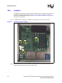
Intel NetStructure® MPCBL0001
High Performance Single Board
Computer
Technical Product Specification
July 2005
Order Number: 273817-007
INFORMATION IN THIS DOCUMENT IS PROVIDED IN CONNECTION WITH INTEL® PRODUCTS. NO LICENSE, EXPRESS OR IMPLIED, BY
ESTOPPEL OR OTHERWISE, TO ANY INTELLECTUAL PROPERTY RIGHTS IS GRANTED BY THIS DOCUMENT. EXCEPT AS PROVIDED IN
INTEL'S TERMS AND CONDITIONS OF SALE FOR SUCH PRODUCTS, INTEL ASSUMES NO LIABILITY WHATSOEVER, AND INTEL DISCLAIMS
ANY EXPRESS OR IMPLIED WARRANTY, RELATING TO SALE AND/OR USE OF INTEL PRODUCTS INCLUDING LIABILITY OR WARRANTIES
RELATING TO FITNESS FOR A PARTICULAR PURPOSE, MERCHANTABILITY, OR INFRINGEMENT OF ANY PATENT, COPYRIGHT OR OTHER
INTELLECTUAL PROPERTY RIGHT.
Intel products are not intended for use in medical, life saving, life sustaining, critical control or safety systems, or in nuclear facility applications. Intel
may make changes to specifications and product descriptions at any time, without notice.
Designers must not rely on the absence or characteristics of any features or instructions marked “reserved” or “undefined.” Intel reserves these for
future definition and shall have no responsibility whatsoever for conflicts or incompatibilities arising from future changes to them.
The Intel NetStructure® MPCBL0001 High Performance Single Board Computer may contain design defects or errors known as errata which may
cause the product to deviate from published specifications. Current characterized errata are available on request.
This document and the software described in it are furnished under license and may only be used or copied in accordance with the terms of the
license. The information in this document is furnished for informational use only, is subject to change without notice, and should not be construed as a
commitment by Intel Corporation. Intel Corporation assumes no responsibility or liability for any errors or inaccuracies that may appear in this
document or any software that may be provided in association with this document. Except as permitted by such license, no part of this document may
be reproduced, stored in a retrieval system, or transmitted in any form or by any means without the express written consent of Intel Corporation.
Contact your local Intel sales office or your distributor to obtain the latest specifications and before placing your product order.
Copies of documents which have an ordering number and are referenced in this document, or other Intel literature may be obtained by calling
1-800-548-4725 or by visiting Intel's website at http://www.intel.com.
AlertVIEW, AnyPoint, AppChoice, BoardWatch, BunnyPeople, CablePort, Celeron, Chips, CT Connect, CT Media, Dialogic, DM3, EtherExpress,
ETOX, FlashFile, i386, i486, i960, iCOMP, InstantIP, Intel, Intel logo, Intel386, Intel486, Intel740, IntelDX2, IntelDX4, IntelSX2, Intel Create & Share,
Intel GigaBlade, Intel InBusiness, Intel Inside, Intel Inside logo, Intel NetBurst, Intel NetMerge, Intel NetStructure, Intel Play, Intel Play logo, Intel
SingleDriver, Intel SpeedStep, Intel StrataFlash, Intel TeamStation, Intel Xeon, Intel XScale, IPLink, Itanium, LANDesk, LanRover, MCS, MMX, MMX
logo, Optimizer logo, OverDrive, Paragon, PC Dads, PC Parents, PDCharm, Pentium, Pentium II Xeon, Pentium III Xeon, Performance at Your
Command, RemoteExpress, Shiva, SmartDie, Solutions960, Sound Mark, StorageExpress, The Computer Inside., The Journey Inside,
TokenExpress, Trillium, VoiceBrick, Vtune, and Xircom are trademarks or registered trademarks of Intel Corporation or its subsidiaries in the United
States and other countries.
† Hyper Threading Technology (HT Technology) requires a computer system with an Intel® Pentium® 4 processor supporting HT Technology and an
HT Technology-enabled chipset, BIOS and operating system. Performance will vary depending on the specific hardware and software you use. See
http://www.intel.com/info/hyperthreading/ for more information including details on which processors support HT Technology.
*Other names and brands may be claimed as the property of others.
Copyright © Intel Corporation, 2005. All rights reserved.
2
Intel NetStructure® MPCBL0001 High Performance Single Board Computer
Technical Product Specification
Contents
Contents
1
Introduction.................................................................................................................................... 11
1.1
1.2
2
Features Overview ........................................................................................................................ 14
2.1
2.2
3
Document Organization ...................................................................................................... 11
Glossary.............................................................................................................................. 12
Application .......................................................................................................................... 14
Functional Description ........................................................................................................ 14
2.2.1 Low Voltage Intel® Xeon™ Processor CPU-0 (U35), CPU-1 (U36) .......................16
2.2.2 Chipset...................................................................................................................17
2.2.2.1 Intel® E7501 Memory Controller Hub (U22)........................................... 17
2.2.2.2 Intel® 82801CA I/O Controller Hub 3 (U7) ............................................. 18
2.2.2.3 Intel® 82870P2 64-bit PCI/PCI-X Controller Hub 2 (U14, U24) ............. 19
2.2.3 Memory (J8, J9, J10, J11) ..................................................................................... 19
2.2.3.1 Memory Ordering Rule for the MCH ...................................................... 20
2.2.4 I/O .......................................................................................................................... 20
2.2.4.1 Super I/O (U28)...................................................................................... 20
2.2.4.2 Real-Time Clock .................................................................................... 21
2.2.4.3 Timer0 Capabilities ................................................................................ 21
2.2.4.4 Gigabit Ethernet (U13) ........................................................................... 21
2.2.4.5 Fibre Channel* (U23) - Optional ............................................................ 22
2.2.5 PMC Connector (J25, J26, J27) ............................................................................ 23
2.2.6 Firmware Hub (U30, U33)...................................................................................... 23
2.2.6.1 FWH 0 (Main BIOS) ............................................................................... 24
2.2.6.2 FWH 1 (Backup/Recovery BIOS)........................................................... 24
2.2.6.3 Flash ROM Backup Mechanism ............................................................ 24
2.2.7 Onboard Power Supplies ....................................................................................... 25
2.2.7.1 Power Feed Fuses ................................................................................. 25
2.2.7.2 ORing Diodes and Circuit Breaker Protection........................................ 25
2.2.7.3 -48 V to +12 V Converter ....................................................................... 25
2.2.7.4 -48 V to +5 V/+3.3 V Converter.............................................................. 25
2.2.7.5 Processor Voltage Regulator Module (VRM) ......................................... 25
2.2.7.6 IPMB Standby Power ............................................................................. 26
Hardware Management Overview ................................................................................................. 27
3.1
3.2
3.3
Sensor Data Record (SDR) ................................................................................................ 28
System Event Log (SEL) .................................................................................................... 30
3.2.1 Temperature and Voltage Sensors ........................................................................ 34
3.2.2 Processor Events................................................................................................... 39
3.2.3 DIMM Memory Events ........................................................................................... 39
3.2.4 System Firmware Progress (POST Error) ............................................................. 39
3.2.5 Critical Interrupts.................................................................................................... 39
3.2.6 System ACPI Power State ..................................................................................... 41
3.2.7 IPMB Link Sensor .................................................................................................. 41
3.2.8 FRU Hot Swap ....................................................................................................... 41
3.2.9 CPU Failure Detection ........................................................................................... 41
3.2.10 Port 80h POST Codes ........................................................................................... 42
Field Replaceable Unit (FRU) Information .......................................................................... 43
Intel NetStructure® MPCBL0001 High Performance Single Board Computer
Technical Product Specification
3
Contents
3.4
3.5
3.6
3.7
3.8
3.9
3.10
3.11
3.12
3.13
3.14
3.15
4
E-Keying ............................................................................................................................. 44
IPMC Firmware Code ......................................................................................................... 44
IPMC Firmware Upgrade Procedure .................................................................................. 45
3.6.1 IPMC Firmware Upgrade Using KCS Interface ..................................................... 45
3.6.2 IPMC Firmware Upgrade via the IPMB Interface (RMCP)..................................... 46
3.6.2.1 Updating MPCBL0001 Firmware ........................................................... 47
OEM IPMI Commands........................................................................................................ 47
3.7.1 Reset BIOS Flash Type ......................................................................................... 47
3.7.2 Set Fibre Channel Port Selection .......................................................................... 48
3.7.3 Get Fibre Channel Port Selection .......................................................................... 48
3.7.4 Get HW Fibre Channel Port Selection ................................................................... 49
3.7.5 Set Control State ................................................................................................... 49
3.7.6 Get Control State ................................................................................................... 50
3.7.7 Get Port80 Data..................................................................................................... 50
Controls Identifier Table...................................................................................................... 50
Hot-Swap Process .............................................................................................................. 51
3.9.1 Hot-Swap LED (DS10)........................................................................................... 52
3.9.2 Ejector Mechanism ................................................................................................ 52
Interrupts and Error Reporting ............................................................................................ 53
3.10.1 Device Interrupts.................................................................................................... 53
3.10.2 Error Reporting ...................................................................................................... 55
ACPI ................................................................................................................................... 56
3.11.1 System States and Power States .......................................................................... 56
Reset Types........................................................................................................................ 56
3.12.1 Reset Logic............................................................................................................ 57
3.12.2 Hard Reset Request .............................................................................................. 57
3.12.3 Soft Reset Request................................................................................................ 57
3.12.4 Warm Boot............................................................................................................. 58
3.12.5 Cold Boot ............................................................................................................... 59
3.12.6 Power Good........................................................................................................... 59
Watchdog Timers (WDTs) .................................................................................................. 62
3.13.1 WDT #1.................................................................................................................. 62
3.13.2 WDT #2.................................................................................................................. 63
3.13.3 WDT #3.................................................................................................................. 63
LED Status.......................................................................................................................... 64
3.14.1 Health LED ............................................................................................................ 64
3.14.2 OOS (Out Of Service) LED.................................................................................... 64
3.14.3 Hot-Swap LED ....................................................................................................... 64
3.14.4 IDE Drive Activity LED ........................................................................................... 65
3.14.5 User Programmable LEDs..................................................................................... 65
3.14.6 Network Link/Speed LEDs..................................................................................... 66
3.14.7 Ethernet Controller Port State LEDs...................................................................... 66
3.14.8 Fibre Channel Port State LEDs ............................................................................. 67
FRU Payload Control.......................................................................................................... 67
3.15.1 Cold Reset ............................................................................................................. 68
3.15.2 Warm Reset........................................................................................................... 68
3.15.3 Graceful Reboot..................................................................................................... 68
3.15.4 Diagnostic Interrupt................................................................................................ 69
Intel NetStructure® MPCBL0001 High Performance Single Board Computer
Technical Product Specification
Contents
4
Connectors .................................................................................................................................... 70
4.1
4.2
4.3
5
Addressing..................................................................................................................................... 85
5.1
5.2
5.3
5.4
6
Configuration Registers ...................................................................................................... 85
5.1.1 Configuration Address Register MCH CONFIG_ADDRESS ................................. 85
5.1.2 Configuration Data Register MCH CONFIG_ADDRESS ....................................... 85
I/O Address Assignments ................................................................................................... 86
Memory Map ....................................................................................................................... 87
IPMC Addresses ................................................................................................................. 88
Specifications ................................................................................................................................ 89
6.1
6.2
6.3
6.4
6.5
7
Backplane Connectors........................................................................................................74
4.1.1 Power Distribution Connector (Zone 1).................................................................. 74
4.1.2 Data Transport Connector (Zone 2)....................................................................... 75
4.1.3 Alignment Blocks ................................................................................................... 76
Front Panel Connectors......................................................................................................77
4.2.1 USB Connector (J12)............................................................................................. 77
4.2.2 Serial Port Connector (J17) ................................................................................... 77
4.2.3 Fibre Channel Small Form-Factor Pluggable (SFP) Receptacle (J34 and J35) .... 80
4.2.4 Fibre Channel SFP Optical Transceiver Module....................................................80
4.2.5 PMC Connectors (J25, J26, J27)........................................................................... 81
On-board Connectors .........................................................................................................84
4.3.1 IDE Connector (J24) ..............................................................................................84
Mechanical Specifications .................................................................................................. 89
6.1.1 Board Outline ......................................................................................................... 89
6.1.2 Backing Plate ......................................................................................................... 92
6.1.3 Component Height ................................................................................................. 92
Environmental Specifications..............................................................................................97
Reliability Specifications ..................................................................................................... 97
6.3.1 Mean Time Between Failure (MTBF) Specifications.............................................. 97
6.3.1.1 Environmental Assumptions .................................................................. 98
6.3.1.2 General Assumptions............................................................................. 98
6.3.1.3 General Notes........................................................................................ 98
6.3.2 Power Consumption ..............................................................................................98
6.3.3 Cooling Requirements ........................................................................................... 99
Board Layer Specifications ................................................................................................. 99
Weight................................................................................................................................. 99
BIOS Features.............................................................................................................................100
7.1
7.2
7.3
7.4
7.5
7.6
7.7
7.8
7.9
Introduction .......................................................................................................................100
BIOS Flash Memory Organization ....................................................................................100
Complementary Metal-Oxide Semiconductor (CMOS) .....................................................100
7.3.1 Copying and Saving CMOS Settings ...................................................................100
Redundant BIOS Functionality .........................................................................................101
System Management BIOS (SMBIOS) .............................................................................101
Legacy USB Support ........................................................................................................102
BIOS Updates...................................................................................................................102
7.7.1 Language Support ...............................................................................................103
Recovering BIOS Data .....................................................................................................103
Boot Options .....................................................................................................................103
Intel NetStructure® MPCBL0001 High Performance Single Board Computer
Technical Product Specification
5
Contents
7.10
7.11
7.12
8
BIOS Setup.................................................................................................................................. 106
8.1
8.2
8.3
8.4
8.5
8.6
9
10.4
10.5
BIOS Configuration........................................................................................................... 132
BIOS Image Updates........................................................................................................ 132
Procedures to Copy and Save BIOS (Including CMOS Settings)..................................... 132
10.3.1 Copying BIOS.bin from the SBC.......................................................................... 132
10.3.2 Saving BIOS.bin to the SBC ................................................................................ 133
10.3.3 Error Messages ................................................................................................... 133
Jumpers ............................................................................................................................ 134
Digital Ground to Chassis Ground Connectivity ............................................................... 136
Maintenance ................................................................................................................................ 137
11.1
11.2
6
BIOS Error Messages....................................................................................................... 127
Port 80h POST Codes ...................................................................................................... 128
Operating the Unit ....................................................................................................................... 132
10.1
10.2
10.3
11
Introduction ....................................................................................................................... 106
Main Menu ........................................................................................................................ 106
Advanced Menu................................................................................................................ 107
8.3.1 CPU Configuration Submenu .............................................................................. 108
8.3.2 IDE Configuration Submenu ................................................................................ 109
8.3.2.1 Primary IDE Master/Slave Submenu ................................................... 110
8.3.3 Floppy Configuration Submenu ........................................................................... 112
8.3.4 SuperIO Configuration Submenu......................................................................... 113
8.3.5 ACPI Configuration Submenu.............................................................................. 114
8.3.5.1 Advanced ACPI Configuration Submenu............................................. 115
8.3.6 System Management Configuration Submenu .................................................... 116
8.3.7 Event Logging Configuration Submenu ............................................................... 117
8.3.8 Fibre Channel Routing (PICMG) Configuration Submenu................................... 118
8.3.9 Remote Access Configuration Submenu............................................................. 119
8.3.10 USB Configuration Submenu............................................................................... 120
8.3.10.1 USB Mass Storage Device Configuration ............................................ 121
8.3.11 PCI Configuration ................................................................................................ 121
Boot Menu ........................................................................................................................ 122
8.4.1 Boot Settings Configuration Submenu................................................................. 122
8.4.2 Boot Device Priority Submenu............................................................................. 123
8.4.3 Hard Disk Drive Submenu ................................................................................... 124
8.4.4 OS Load Timeout Timer ...................................................................................... 124
Security Menu................................................................................................................... 125
Exit Menu.......................................................................................................................... 125
Error Messages ........................................................................................................................... 127
9.1
9.2
10
7.9.1 CD-ROM and Network Boot ................................................................................ 103
7.9.2 Booting without Attached Devices ....................................................................... 103
Fast Booting Systems....................................................................................................... 104
7.10.1 Quick Boot ........................................................................................................... 104
BIOS Security Features .................................................................................................... 104
Remote Access Configuration .......................................................................................... 105
Supervision ....................................................................................................................... 137
Diagnostics ....................................................................................................................... 137
11.2.1 In-Target Probe (ITP)........................................................................................... 137
Intel NetStructure® MPCBL0001 High Performance Single Board Computer
Technical Product Specification
Contents
12
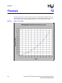
Thermals......................................................................................................................................138
13
Component Technology ..............................................................................................................139
14
Warranty Information ...................................................................................................................140
14.1
14.2
14.3
15
Intel NetStructure® Compute Boards and Platform Products Limited Warranty ..............140
Returning a Defective Product (RMA) ..............................................................................140
For the Americas ..............................................................................................................141
14.3.1 For Europe, Middle East, and Africa (EMEA) ......................................................141
14.3.2 For Asia and Pacific (APAC)................................................................................141
Customer Support .......................................................................................................................143
15.1
15.2
15.3
15.4
Customer Support.............................................................................................................143
Technical Support and Return for Service Assistance .....................................................143
Sales Assistance ..............................................................................................................143
Product Code Summary ...................................................................................................143
16
Certifications................................................................................................................................144
17
Agency Information—Class A......................................................................................................145
17.1
17.2
17.3
17.4
17.5
17.6
17.7
18
Agency Information—Class B......................................................................................................148
18.1
18.2
18.3
18.4
18.5
18.6
19
North America (FCC Class A)...........................................................................................145
Canada – Industry Canada (ICES-003 Class A) (English and French-translated) ...........145
Safety Instructions (English and French-translated) .........................................................145
17.3.1 English .................................................................................................................145
17.3.2 French..................................................................................................................146
Taiwan Class A Warning Statement .................................................................................146
Japan VCCI Class A .........................................................................................................147
Korean Class A.................................................................................................................147
Australia, New Zealand.....................................................................................................147
North America (FCC Class B)...........................................................................................148
Canada – Industry Canada (ICES-003 Class B) (English and French-translated) ...........148
Safety Instructions (English and French-translated) .........................................................148
18.3.1 English .................................................................................................................148
18.3.2 French..................................................................................................................149
Japan VCCI Class B .........................................................................................................149
Korean Class B.................................................................................................................150
Australia, New Zealand.....................................................................................................150
Safety Warnings ..........................................................................................................................151
19.1
19.2
19.3
19.4
19.5
Mesures de Sécurité .........................................................................................................152
Sicherheitshinweise ..........................................................................................................154
Norme di Sicurezza ..........................................................................................................156
Instrucciones de Seguridad ..............................................................................................158
Chinese Safety Warning ...................................................................................................160
A
Reference Documents.................................................................................................................161
B
List of Supported Commands (IPMI v1.5 and PICMG 3.0)..........................................................163
Intel NetStructure® MPCBL0001 High Performance Single Board Computer
Technical Product Specification
7
Contents
Tables
1
2
3
4
5
6
7
8
9
10
11
12
13
14
15
16
17
18
19
20
21
22
23
24
25
26
27
28
29
30
31
32
33
34
35
36
37
38
39
40
41
42
43
44
45
46
47
48
49
8
P64H2 Interfaces........................................................................................................................ 19
Hardware Sensors...................................................................................................................... 28
SEL Events Supported by the MPCBL0001 SBC....................................................................... 31
Sensor Thresholds for IPMC Firmware 1.0 ................................................................................ 35
Sensor Thresholds for IPMC Firmware 1.2 ................................................................................ 36
Sensor Thresholds for IPMC Firmware 1.7 and Above .............................................................. 37
Sensor Thresholds for IPMC Firmware 1.14 and Above ............................................................ 38
PCI Mapping for Hardware Component Subsystem................................................................... 40
CPU Failure Behavior ................................................................................................................. 42
FRU Multirecord Data for CPU/RAM/PMC/BIOS Version Information ....................................... 43
PMC Data ................................................................................................................................... 43
Link Descriptors for E-Keying ..................................................................................................... 44
Reset BIOS Flash Type .............................................................................................................. 47
Set Fibre Channel Port Selection ............................................................................................... 48
Get Fibre Channel Port Selection ............................................................................................... 48
Get HW Fibre Channel Port Selection ........................................................................................ 49
Set Control State ........................................................................................................................ 49
Get Control State ........................................................................................................................ 50
Get Port80 Data.......................................................................................................................... 50
Controls Identifier Table ............................................................................................................. 50
Hot-Swap LED (DS11) ............................................................................................................... 52
Interrupt Assignments................................................................................................................. 53
Power States and Targeted System Power................................................................................ 56
Reset Request............................................................................................................................ 58
Reset Actions ............................................................................................................................. 59
Health LED ................................................................................................................................. 64
OOS LED (DS9) ......................................................................................................................... 64
IDE Drive Activity LED ................................................................................................................ 65
User Programmable LEDs.......................................................................................................... 65
GPIO Pin Connections ............................................................................................................... 65
Network Link LEDs ..................................................................................................................... 66
Network Speed LEDs ................................................................................................................. 66
Ethernet Controller Port State LED ............................................................................................ 67
Fibre Channel Port State LED (DS2, DS3)................................................................................. 67
CMM Commands for FRU Control Options ................................................................................ 67
Returned Values from the Get Message Command................................................................... 69
LED Descriptions ........................................................................................................................ 73
Connector Assignments ............................................................................................................. 73
Power Distribution Connector (Zone 1) P10 Pin Assignments ................................................... 74
Data Transport Connector (Zone 2) P23 Pin Assignments ........................................................ 76
USB Connector (J12) Pin Assignments...................................................................................... 77
Serial Port Connector (J17) Pin Assignments ............................................................................ 78
Fibre Channel SFP Copper Transceiver Module (AMP, J34, J35) ............................................. 80
Fibre Channel SFP Pin Assignments ......................................................................................... 81
PMC Connector Pin Assignments - 32 Bit .................................................................................. 82
PMC Connector Pin Assignments - 64 Bit .................................................................................. 83
IDE Connector Pin Assignments ................................................................................................ 84
Configuration Address Register Bit Assignments ....................................................................... 85
Configuration Data Register Bit Assignments ............................................................................ 86
Intel NetStructure® MPCBL0001 High Performance Single Board Computer
Technical Product Specification
Contents
50
51
52
53
54
55
56
57
58
59
60
61
62
63
64
65
66
67
68
69
70
71
72
73
74
75
76
77
78
79
80
81
82
83
84
85
87
86
88
89
90
91
92
93
94
95
96
97
98
I/O Address Cross-References................................................................................................... 86
Memory Map............................................................................................................................... 87
SMBus Addresses ...................................................................................................................... 88
Environmental Specifications...................................................................................................... 97
Reliability Estimate Data............................................................................................................. 97
Total Measured Power................................................................................................................ 98
Supervisor and User Password Functions................................................................................105
Function Key Escape Code Equivalents...................................................................................105
BIOS Setup Program Menu Bar ...............................................................................................106
BIOS Setup Program Function Keys ........................................................................................106
Main Menu ................................................................................................................................107
Advanced Menu........................................................................................................................108
CPU Configuration Submenu ...................................................................................................109
IDE Configuration Submenu .....................................................................................................109
Primary IDE Master/Slave Submenu ........................................................................................111
Floppy Configuration Submenu ................................................................................................112
SuperIO Configuration Submenu..............................................................................................113
ACPI Configuration Submenu...................................................................................................114
Advanced ACPI Configuration Submenu..................................................................................115
System Management Configuration Submenu .........................................................................116
Event Logging Configuration Submenu ....................................................................................117
Fibre Channel Routing (PICMG) Submenu ..............................................................................118
Remote Access Configuration Submenu..................................................................................119
USB Configuration Submenu....................................................................................................120
USB Mass Storage Device Configuration.................................................................................121
PCI Configuration Submenu .....................................................................................................122
Boot Menu ................................................................................................................................122
Boot Settings Configuration Submenu......................................................................................123
Boot Device Priority Submenu..................................................................................................124
Hard Disk Drive Priority Submenu ............................................................................................124
OS Load Timeout Timer Submenu ...........................................................................................125
Security Menu...........................................................................................................................125
Exit Menu..................................................................................................................................126
BIOS Error Messages...............................................................................................................127
Bootblock Initialization Code Checkpoints................................................................................128
POST Code Checkpoints..........................................................................................................129
ACPI Runtime Checkpoints ......................................................................................................131
DIM Code Checkpoints.............................................................................................................131
BIOS Beep Codes ....................................................................................................................131
Error Message ..........................................................................................................................133
J18 Pin Assignments ................................................................................................................135
J16 Jumper Assignments .........................................................................................................135
J37 Jumper assignments..........................................................................................................135
J40 Jumper Assignments .........................................................................................................136
Hardware Monitoring Components ...........................................................................................137
Main Components.....................................................................................................................139
MPCBL0001 Product Code Summary ......................................................................................143
IPMI 1.5 Supported Commands ...............................................................................................163
PICMG 3.0 IPMI Supported Commands...................................................................................165
Intel NetStructure® MPCBL0001 High Performance Single Board Computer
Technical Product Specification
9
Contents
Figures
1
2
3
4
5
6
7
8
9
10
11
12
13
14
15
16
17
18
19
20
21
22
23
24
25
26
27
28
29
Intel NetStructure® MPCBL0001 SBC Block Diagram............................................................... 15
Memory Ordering........................................................................................................................ 20
Hardware Management Block Diagram...................................................................................... 27
IPMC Firmware Code Process ................................................................................................... 45
Upgrade via Remote Management Node ................................................................................... 46
Hot-Swap Process...................................................................................................................... 51
Interrupt Signals ......................................................................................................................... 54
Power Good Map........................................................................................................................ 59
Reset Chain................................................................................................................................ 61
Watchdog Timers ....................................................................................................................... 62
Flow Diagram for Graceful Reboot Command ........................................................................... 68
Diagnostic Interrupt Command Implementation ......................................................................... 69
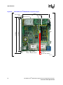
MPCBL0001 SBC Connector Locations..................................................................................... 70
MPCBL0001NXX SBC Front Panel............................................................................................ 71
MPCBL0001FXX SBC Front Panel ............................................................................................ 72
Power Distribution Connector (Zone 1) P10 ............................................................................... 74
Data Transport Connector (Zone 2) J23..................................................................................... 75
Serial Port Connector (J17) ........................................................................................................ 78
DB9 to RJ-45 Pin Translation ..................................................................................................... 79
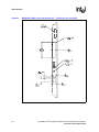
Intel NetStructure® MPCBL0001 Component Layout ................................................................ 90
Intel NetStructure® MPCBL0001 Component Layout ................................................................ 91
MPCBL0001 SBC Front Panel Dimensions – FC SKU (PMC and Connectors) ........................ 93
MPCBL0001 SBC Front Panel Dimensions – FC SKU (Screws and LEDs) .............................. 94
MPCBL0001 SBC Front Panel Dimensions – Non FC SKU (PMC and Connectors) ................. 95
MPCBL0001 SBC Front Panel Dimensions – Non-FC SKU (Screws and LED) ........................ 96
Low Voltage Intel® Xeon™ Processor Heatsink......................................................................... 99
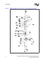
Jumper/Connector Locations.................................................................................................... 134
Connecting Digital Ground to Chassis Ground......................................................................... 136
Power vs. Flow Rate................................................................................................................. 138
Revision History
Date
10
Revision
Description
July 2005
007
Added Table 7. Modified tables 3, 9, 13, 14, and 53; Fig. 21; and Section 10.5.
April 2005
006
New text in sections 3.2.9, 6.5, 10.3.1, and tables 2, 3, and 6.
February 2005
005
New text, figures; added Section 18, “Agency Information—Class B”.
November 2004 004
Changes to figures 12, 13; changes to table 2, 3, 48, 77 and 81; added example
to Section 3.2.5.
June 2004
SRA Release - changed from release 002 to current.
003
January 2004
002
Pre-SRA Release.
October 2003
001
Initial public release of this document
Intel NetStructure® MPCBL0001 High Performance Single Board Computer
Technical Product Specification
Introduction
Introduction
1.1
1
Document Organization
This document gives technical specifications related to the Intel NetStructure® MPCBL0001 High
Performance Single Board Computer. The MPCBL0001 is designed following the standards of the
Advanced Telecommunications Compute Architecture (AdvancedTCA*) Design Guide for high
availability, switched network computing. This document is intended for support during system
product development and while sustaining a product. It specifies the architecture, design
requirements, external requirements, board functionality, and design limitations of the
MPCBL0001 Single Board Computer.
The following summarizes the focus of each chapter in this document.
Chapter 1, “Introduction” gives an overview of the information contained in the Intel
NetStructure® MPCBL0001 High Performance Single Board Computer Technical Product
Specification as well as a glossary of acronyms and important terms.
Chapter 2, “Features Overview” introduces the key features of the MPCBL0001. It includes a
functional block diagram and a brief description of each block.
Chapter 3, “Hardware Management Overview”provides a high-level overview related to IPMI
implementation based on PICMG* 3.0 and IPMI v1.5 specifications in the MPCBL0001 SBC.
Chapter 4, “Connectors” includes an illustration of connector locations, connector descriptions,
and pinout tables.
Chapter 5, “Addressing” summarizes the information you need to configure the MPCBL0001.
Included are the PCI configuration map, Configuration Address register, Configuration Data
register, I/O address assignments, memory map, and IPMC addresses.
Chapter 6, “Specifications” contains the mechanical, environmental, and reliability specifications
for the MPCBL0001.
Chapter 7, “BIOS Features” provides an introduction to the Intel/AMI BIOS, and the System
Management BIOS, stored in flash memory on the MPCBL0001.
Chapter 8, “BIOS Setup” describes the interactive menu system of the BIOS Setup program. The
menu allows a user to configure the BIOS for a given system.
Chapter 9, “Error Messages” lists BIOS error messages, Port 80h POST codes, and bus
initialization checkpoints, and provides a brief description of each.
Chapter 10, “Operating the Unit” provides specifics for configuring the MPCBL0001, including
BIOS configuration and jumper settings.
Chapter 11, “Maintenance” includes supervision and diagnostics information.
Chapter 13, “Component Technology” lists the major components used on the MPCBL0001.
Intel NetStructure® MPCBL0001 High Performance Single Board Computer
Technical Product Specification
11
Introduction
Chapter 14, “Warranty Information” provides warranty information for Intel® NetStructureTM
products.
Chapter 15, “Customer Support” provides information on how to contact customer support.
Chapter 16, “Certifications” and Chapter 17, “Agency Information—Class A” document the
regulatory requirements the MPCBL0001 is designed to meet.
Appendix A, “Reference Documents” provides a list of data sheets, standards, and specifications
for the technology designed into the MPCBL0001.
Appendix B, “List of Supported Commands (IPMI v1.5 and PICMG 3.0)”provides lists of
commands supported by IPMI v1.5 and PICMG Specification 3.0.
1.2
Glossary
For ease of use, numeric entries are listed first with alpha entries following. Acronyms and terms
are then entered in their respective place.
ACPI
Advanced Configuration and Power Interface.
AdvancedTCA
Advanced Telecommunications Compute Architecture
BIOS
Basic Input/Output Subsystem. ROM code that initializes the computer
and performs some basic functions.
Blade
An assembled PCB card that plugs into a chassis.
DIMM
Dual Inline Memory Module. Small card with memory on it used for
MPCBL0001.
DMI
Desktop Management Interface
EEPROM
Electrically Erasable Programmable Read-Only Memory
Fabric Board
A board capable of moving packet data between Node Boards via the
ports of the backplane. This is sometimes referred to as a switch.
Fabric Slot
A slot supporting a link port connection to/from each Node Slot and/or
out of the chassis.
Hyper-Threading Technology†
HT Technology allows a single (or dual) physical processor, to appear as
two (or quad) logical processors to a HT Technology-aware operating
system.
12
I2C*
Inter-IC [Integrated Circuit]. 2-wire interface commonly used to carry
management data.
IBA
Intel® Boot Agent. The Intel Boot Agent is a software product that
allows your networked client computer to boot using a program code
image supplied by a remote server.
IDE
Integrated Device Electronics. Common, low-cost disk interface.
IPMB
Intelligent Platform Management Bus. Physical 2-wire medium to carry
IPMI.
Intel NetStructure® MPCBL0001 High Performance Single Board Computer
Technical Product Specification
Introduction
IPMC
Intelligent Platform Management Controller. ASIC in baseboard
responsible for low-level system management.
IPMI
Intelligent Platform Management Interface. Programming model for
system management.
KCS
Keyboard Controller Style interface.
LPC Bus
Los Pin Count Bus. Legacy I/O bus that replaces ISA and X-bus. See the
Low Pin Count (LPC) Interface Specification.
MTBF
Mean Time Between Failure. A reliability measure based on the
probability of failure.
NEBS
National Equipment Building Standards. Telco standards for equipment
emissions, thermal, shock, contaminants, and fire suppression
requirements.
NMI
Non-Maskable Interrupt. Low-level PC interrupt.
Node Board
A board capable of providing and/or receiving packet data to/from a
Fabric Board via the ports of the networks. The term is used
interchangeably with SBC.
MPCBL0001
Single or dual processor Single Board Computer with Fibre Channel.
MPCBL0002
Single or dual processor Single Board Computer without Fibre Channel.
Node Slot
A slot supporting port connections to/from Fabric Slot(s). A Node slot is
intended to accept a Node Board
Physical Port
A port that physically exists. It is supported by one of many physical
(PHY) type components.
PMC
PCI Mezzanine Card. IEEE1386 standard for embedded PCI cards. They
mount parallel to the SBC.
ROM
Read-Only Memory.
SBC
Single Board Computer. This term is used interchangeably with Node
Board.
SEL
System Event Log. Action logged by management controller.
SFP
Small Form Factor Pluggable receptacle for the front panel Fibre
Channel interfaces.
SMBus
System Management Bus. Similar to I2C
SMI
System Management Interrupt. Low-level PC interrupt which can be
initiated by chipset or management controller. Used to service IPMC or
handle things like memory errors.
SMS, SMSC
Standard Microsystems Corporation*
USB
Universal Serial Bus. General-purpose peripheral interconnect,
operating at 1-12 Mbps.
Intel NetStructure® MPCBL0001 High Performance Single Board Computer
Technical Product Specification
13
Features Overview
Features Overview
2.1
2
Application
The Advanced Telecommunications Compute Architecture (AdvancedTCA) standards define open
architecture modular computing components for carrier-grade, communications network
infrastructure. The goals of the standards are to enable blade-based modular platforms to be:
•
•
•
•
cost effective
high-density
high-availability
scalable
These systems use a fabric I/O network for connecting multiple, independent processor boards, I/O
nodes (e.g., line cards), and I/O devices (e.g., storage subsystem).
The MPCBL0001 SBC is designed per the AdvancedTCA Design Guide for High Availability,
Switched Network Computing. Bulk storage for the system is connected through optional dual
Fibre Channel interfaces. The MPCBL0001FXX SBC includes a Fibre Channel controller. The
MPCBL0001NXX SBC does not have the Fibre Channel controller.
2.2
Functional Description
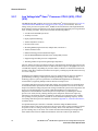
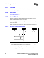
This topic defines the architecture of the MPCBL0001 SBC through descriptions of functional
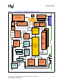
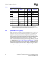
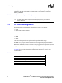
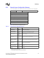
blocks. Figure 1, “Intel NetStructure® MPCBL0001 SBC Block Diagram” on page 15 shows the
functional blocks of the MPCBL0001 SBC. The MPCBL0001 SBC is a dual processor, hotswappable SBC with backplane connections to dual Gigabit Ethernet star networks and dual Fibre
Channel star arbitrated loops.
The SBC incorporates an Intelligent Platform Management Controller that monitors critical
functions of the board, responds to commands from the shelf manager, and reports events.
Power is supplied to the MPCBL0001 SBC through two redundant -48 V power supply
connections. Power for on-board hardware management circuitry is provided through a standby
converter on the power mezzanine. This converter, along with all the other converters on the power
mezzanine are fed by the diode OR'd -48 V supply from the backplane.
The SBC has provision for the addition of a PMC device and supports 32-bit and 64-bit transfers at
33 MHz and 66 MHz. The SBC also offers one USB and one service terminal interface. An
overview of each block follows.
14
Intel NetStructure® MPCBL0001 High Performance Single Board Computer
Technical Product Specification
Features Overview
Intel NetStructure® MPCBL0001 SBC Block Diagram
Figure 1.
Optional
Optional2.5”
2.5”
Hard
Hard Disk
DiskDrive
Drive
-48V
P10
IPMB-A
IPMB
IPMB Isolators
Isolators
IPMB
IPMB Isolators
Isolators IPMB-B
Intel
Intel
82802AC
82802AC
(FWH0)
(FWH0)
Intel
Intel
82802AC
82802AC
(FWH1)
(FWH1)
SMBUS
Standard
Standard
Microsystems
Microsystems Corp.
Corp.
LPC47B272
LPC47B272 Super
Super I/O
I/O
On-board
On-board Power
Power
Supplies
Supplies and
and Hot
Hot
Swap
Swap Circuitry
Circuitry
Sahalee
IPMC
Sahalee
IPMC
IPMC
33 MHz
LPC
(4MB/s)
RJ-45
RJ-45
Serial
Serial
Port
Port
ATA
33/66/100
ADM
ADM
1026
1026
USB
USB
Port
Port
Intel®
Intel® ICH3
ICH3
528 MB/s
PCI 64/66
Intel®
Intel®
P64H2
P64H2
PCI
PCI
Bridge
Bridge
Intel®
Intel®
82546EB
82546EB
Dual
DualGb
Gb
Ethernet
Ethernet
266 MB/s HI 1.5
1066
MB/s
HI-2
Intel®
Intel®
P64H2
P64H2
PCI
PCI
Bridge
Bridge
1066
MB/s
HI-2
1066 MB/s
PCI-X
256K
256KSRAM
SRAM
256K
256K SRAM
SRAM
Four
Four
184-pin
184-pin
DIMM
DIMM
Sockets
Sockets
DDR-266
DDR-266
ECC
ECC
SDRAM
SDRAM
Intel®
Intel® E7501
E7501
Memory
Memory
Controller
ControllerHub
Hub
(MCH)
(MCH)
QLogic
QLogic
ISP2312
ISP2312
Fibre
Fibre
Channel
Channel
Controller
Controller
2.1 GB/s
DDR-266 2.1 GB/s
DDR-266
Backplane
Front Panel
1066 MB/s
PCI-X
PCI
PCI
Optional
Mezzanine
Mezzanine
ThirdCard
Card
party
(PMC)
(PMC)
PMC
Connector
Connector
J23
400MT/s 3.2GB/s
Dual FC Ports
MUX
MUX
Dual FC
Ports
Dual
Dual SFP
SFP
Connectors
Connectors
MPCBL0001Fxx
products only
Low
LowVoltage
Voltage
Intel®
Intel®Xeon™
Xeon™
Processor
Processor
Low
LowVoltage
Voltage
Intel®
Intel® Xeon™
Xeon™
Processor
Processor
Dual Fibre Channel Ports to Fabric Interface
Dual Gigabit Ethernet Ports to Base Interface
Intel NetStructure® MPCBL0001 High Performance Single Board Computer
Technical Product Specification
15
Features Overview
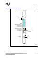
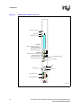
2.2.1
Low Voltage Intel® Xeon™ Processor CPU-0 (U35), CPU-1
(U36)
The MPCBL0001 SBC supports up to two Low Voltage Intel® Xeon™ processors (see Figure 20,
“Intel NetStructure® MPCBL0001 Component Layout” on page 90 for locations). The Low
Voltage Xeon processor incorporates Intel® NetBurst™ microarchitecture and a high-bandwidth
Front-Side Bus, allowing performance levels that are significantly higher than previous generations
of IA-32 family processors. The processors include the following features:
•
•
•
•
•
•
•
•
•
•
•
2.0 GHz with a 400 MHz system bus
512 Kbyte L2 cache
Hyper-pipelined technology
Advanced dynamic execution
Execution trace cache
Streaming SIMD (single instruction, multiple data) extensions 2
Advanced transfer cache
Enhanced floating point and multimedia engine
Intel & OEM EEPROM and thermal sensor manageability features
Supports single and dual processor configurations
Throttling enabled for protection against high temperatures
The Low Voltage Xeon processor host bus utilizes a split-transaction, deferred-reply protocol. The
host bus uses source-synchronous transfer of address and data to improve throughput at the 100 or
133 MHz bus frequency (depending on processor model). Addresses are transferred at 2X the bus
frequency while data is transferred at 4X the bus frequency, resulting in peak data transfer rates up
to 3.2 or 4.3 GBytes/s.
In addition to the NetBurst microarchitecture, the Low Voltage Intel Xeon processor includes a
groundbreaking technology called Hyper-Threading Technology† (HT Technology). HT
Technology improves processor performance for multithreaded applications or multitasking
environments by supporting multiple software threads on each processor.
Low Voltage Intel Xeon processors require their package case temperatures to be operated below
an absolute maximum specification. If the chassis ambient temperature exceeds a level whereby
the processor thermal cooling subsystem can no longer maintain the specified case temperature, the
processors will automatically enter a mode called Thermal Monitor to reduce their case
temperatures. Thermal Monitor controls the processor temperature by modulating the internal
processor core clocks, thereby reducing internal power dissipation, and does not require any
interaction by the Operating System or Application. Once the case temperatures have reached a
safe operating level, the processor will return to its non-modulated operating frequency. See the
Low Voltage Intel Xeon processor datasheet, referenced in Appendix A, “Reference Documents”,
for further details.
An optional ITP700 port connection is included to facilitate debug and BIOS/software
development efforts. This JTAG connection to the processors utilizes voltage-signaling levels that
are specific to the Low Voltage Xeon processor family. These levels must not be exceeded or
processor damage may occur. Please refer to Intel document ITP700 Debug Port Design Guide,
order number 249679-005 for additional information on the ITP connector pin definitions.
16
Intel NetStructure® MPCBL0001 High Performance Single Board Computer
Technical Product Specification
Features Overview
2.2.2
Chipset
The Intel® E7501 chipset consists of three major components:
• Intel® E7501 Memory Controller Hub (MCH)
• Intel® 82801CA I/O Controller Hub 3 (ICH3)
• Intel® 82870P2 64-bit PCI/PCI-X Controller Hub 2 (P64H2)
See Figure 20, “Intel NetStructure® MPCBL0001 Component Layout” on page 90 for their
locations.
2.2.2.1
Intel® E7501 Memory Controller Hub (U22)
The Intel® E7501 Memory Controller Hub (MCH) interfaces between the processor system bus
and the memory and I/O subsystems.
Significant features are listed below:
• System/host bus features:
— Supports dual processors at either 400 or 533 MT/s or a bandwidth of 3.2 or 4.3 GBytes/s
— Supports a 36-bit system bus addressing model
— 12 deep in-order queue, two deep defer queue
Note:
The current MPCBL0001 is designed to run with the Intel® LV Xeon® 2.0 GHz processor. At this
processor frequency, the processor side bus (PSB) will run at 400 MT/s with a bandwidth of 3.2
GBytes/s.
• Memory subsystem features:
— 144-bit wide (72-bit x 2), DDR-266 memory interfaces with 3.2 or 4.3 GByte/s bandwidth
— Supports x72, registered DDR-266 ECC DIMMs using 64-, 128-, 256-, and 512-Mbit
SDRAMs
— Supports a maximum of 16 GBytes of memory (MPCBL0001 SBC implementation
supports a maximum of 8 Gbytes).
— Supports S4EC/D4ED ChipKill* ECC (x4 ChipKill)
• Corrects all bit errors within a single 4-bit nibble
• Detects all errors contained within two 4-bit nibbles
• Memory scrubbing supported
— Supports up to 32 simultaneous open pages
— Hardware support for auto-initialization of memory with valid ECC
• I/O features:
— Hub interface A provides HI 1.5 connection for ICH3
• 266 MB/s data bandwidth with parity protection
• 8 bits wide, 66 MHz clock, 4x data transfer (quad-pumped)
• Supports 64-bit inbound addressing, 32-bit outbound addressing
— Hub interfaces B and C provide HI2.0 connections for two P64H2s
• 1 GByte/s data bandwidth with ECC protection in each direction
Intel NetStructure® MPCBL0001 High Performance Single Board Computer
Technical Product Specification
17
Features Overview
• 16-bits wide, 66 MHz clock, 8x data transfer (octal pumped)
• Supports 64-bit inbound, 32-bit outbound addressing
The MCH I/O subsystems interface incorporates four hub interfaces. Each Hub interface is a pointto-point connection between the MCH and an I/O bridge/device. The various components of the
chipset communicate via these connected hub interfaces:
• The first hub link connects the MCH to the ICH3.
• The next two hub link interfaces connect the MCH to P64H2 components.
• The remaining hub link is unused.
2.2.2.2
Intel® 82801CA I/O Controller Hub 3 (U7)
The Intel® 82801CA I/O Controller Hub 3 (IHC3) provides the legacy I/O subsystem and
integrates advanced I/O functions. ICH3 features are listed below:
• IDE interface controller
• Three Universal Host Controller Interface (UHCI)
• USB host controllers supporting up to 6 ports (MPCBL0001 SBC implementation supports
one port on the front panel)
•
•
•
•
•
•
Integrated I/O APIC
SMBus 2.0 controller
LPC interface
Watchdog timer #3 (see “Watchdog Timers (WDTs)” on page 62)
PCI 2.2 bus interface supporting 32bit/33 MHz operation
Connects to MCH through Hub Interface A (HI 1.5)
The MPCBL0001 SBC implements one USB port and does not use the ICH3 PCI connection.
2.2.2.2.1
PCI Bus Master IDE Interface (J24)
The ICH3 acts as a PCI based, enhanced IDE, 32-bit interface controller for intelligent disk drives
that have disk controller electronics onboard. The SBC includes a single 40-pin (2 x 20) IDE
connector (J24) that supports one master or one slave device. See Figure 20, “Intel NetStructure®
MPCBL0001 Component Layout” on page 90 drawing for its location. The IDE controller
provides support for an internally mounted 2.5” hard disk. The IDE controller has the following
features:
•
•
•
•
•
•
Note:
18
PIO and DMA transfer modes
Mode 4 timings
Supports Ultra ATA33/66/100 synchronous DMA
Buffering for PCI/IDE burst transfers
Master/slave IDE mode
Support for up to two devices (Master/Slave) via a single primary IDE connector
(MPCBL0001 SBC implementation supports one optional physical 2.5" IDE device)
Incorporating an optional IDE Hard Disk drive may significantly impact the Reliability
Specifications in Section 6.3.
Intel NetStructure® MPCBL0001 High Performance Single Board Computer
Technical Product Specification
Features Overview
Note:
2.2.2.3
Performance of the IDE interface may be impacted by the DMA mode and type of DMA transfers
used. Even though the BIOS automatically sets the DMA mode/type, the OS could downgrade the
DMA transfer mode. Check the operating system documentation to see what DMA mode is used
by default and whether it is possible to change to a higher performance DMA mode.
Intel® 82870P2 64-bit PCI/PCI-X Controller Hub 2 (U14, U24)
The two P64H2 devices provide the system’s high-performance PCI bus support. See Figure 20,
“Intel NetStructure® MPCBL0001 Component Layout” on page 90 for their locations. Each
P64H2 component supports two independent, 64-bit, PCI/PCI-X interfaces. 32-bit/33 MHz and 64bit/66 MHz PCI bus modes are also supported. Each PCI bus interface features:
•
•
•
•
•
•
•
PCI-X 1.0 Specification compliance
PCI Specification 2.2 compliance
PCI-PCI Bridge Rev 1.1 compliance
PCI Hot Plug 1.0 compliance
I/O APIC supporting up to 24 interrupts (16 external pins)
PCI peer-to-peer write capability between PCI ports
SMBus target for Out-of-Band access to all internal PCI registers
Each of the two P64H2 devices (U14, U24) included on the MPCBL0001 SBC provides the bridge
to two independent PCI bus connections, as shown in Table 1, “P64H2 Interfaces” on page 19.
Table 1.
P64H2 Interfaces
P64H2 Device
U24
U14
Interface
PCI-X interface to the optional dual Fibre Channel controller
• PCI-X interface to the dual Gigabit Ethernet controller
• 64-bit/66 MHz PCI bus for a plug-in PMC card
The two high-speed communications interfaces (Gigabit Ethernet and Fibre Channel) are located in
separate P64H2 devices to maximize data throughput. A single HI-2 hub link connection from the
P64H2 to the MCH provides a >1 Gbyte/s bandwidth back to memory and the processor System
Bus.
2.2.3
Memory (J8, J9, J10, J11)
Four DDR 266 DIMM sockets make up the memory subsystem. See Figure 20, “Intel
NetStructure® MPCBL0001 Component Layout” on page 90 for their locations. The MCH defines
two memory channels operating in parallel to logically create a 144-bit wide memory data path.
ECC is generated and checked across 128 bits of data, allowing for significant improvement in
error correction.
Due to this architecture, DDR DIMMs must be installed in matched pairs. Memory DIMM
configurations ranging from 512 MBytes to 8 GBytes in 512 MByte increments are supported.
Intel NetStructure® MPCBL0001 High Performance Single Board Computer
Technical Product Specification
19
Features Overview
2.2.3.1
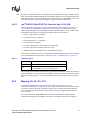
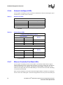
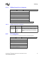
Memory Ordering Rule for the MCH
Platforms based on the E7501 chipset require DDR DIMMs to be populated in matched pairs in a
specific order. Start with the two DIMMs furthest from the MCH in a “fill-farthest” approach (see
Figure 2). This requirement is based on the signal integrity requirements of the DDR interface.
Figure 2.
Memory Ordering
Fill
Last
MCH, U22
J8
Fill
First
J9
J10
J11
B0894-01
2.2.4
I/O
2.2.4.1
Super I/O (U28)
The Super I/O device (SIO) is an SMSC LPC47B272 enhanced Super I/O controller. The SIO
connects to the ICH3 through its LPC bus connection. The SIO provides support for the front panel
serial port (J17, see page 70). There is no front-panel connection to the legacy keyboard and mouse
PS/2 ports. Keyboard and mouse support are provided by the USB connection (J12, see page 77).
See Figure 13 for connector locations.
20
Intel NetStructure® MPCBL0001 High Performance Single Board Computer
Technical Product Specification
Features Overview
To facilitate debug and BIOS development, SIO connections such as legacy (PS/2) keyboard/
mouse and floppy may be provided on initial board revisions. Software must not rely on the
presence of these connections on future board revisions.
2.2.4.2
Real-Time Clock
The MPCBL0001 SBC real-time clock is integrated into the ICH3. It is derived from a 32.768 KHz
crystal with the following specifications:
•
•
•
•
Frequency tolerance @ 25 ºC: ±20ppm
Frequency stability: maximum of -0.04ppm/(ΔºC)2
Aging ΔF/f (1st year @ 25 ºC): ±3ppm
±20ppm from 0-55 ºC and aging 1ppm/year
The real-time clock is powered by a 0.22F SuperCap* capacitor when main power is not applied to
the board. This capacitor powers the real-time clock for a minimum of two hours while external
power is removed from the MPCBL0001 SBC.
See Section 3.13, “Watchdog Timers (WDTs)” on page 62 for information about the real-time
clock timers.
2.2.4.3
Timer0 Capabilities
Timer0, integrated inside the ICH3, is an 8254 compatible timer. This timer is set up to generate a
periodic waveform that creates the edge for the timer0 interrupt. The interrupt is received by the
ICH3 APIC and communicated to the CPU(s).
MPCBL0001 provides a high-precision 14.318 MHz crystal clock source as the reference for the
timer0 counters. To improve timing accuracy, the crystal used is a low-PPM, high-stability
component with the following specifications:
• Frequency tolerance (25º C): ±10ppm
• Temperature characteristics (-10º C to +60º C): ±5ppm
• Aging: ±1ppm per year max
This timer does not operate when board power is removed.
2.2.4.4
Gigabit Ethernet (U13)
The MPCBL0001 SBC implements two Gigabit Ethernet interfaces, each of which is routed to the
fabric/switch slot through the backplane (J23, see page 75). There are no direct, external Ethernet
ports included on the SBC board. Each Ethernet connection utilizes an 82546 Dual Gigabit
Ethernet Controller, allowing support for 1000Mbits/s, 100Mbits/s and 10Mbits/s data rates.
The 82546 controller is optimized for designs using the PCI and the emerging PCI-X bus interface
extension. The MPCBL0001 SBC has a 133 MHz PCI-X bus connection. The integrated physical
layer circuitry (PHY) provides an IEEE 802.3 Ethernet Interface for 1000Base-T, 100Base-TX,
and 10Base-T applications.
Features include:
• 32/64-bit 33/66 MHz, PCI Rev 2.2 compliant interface
Intel NetStructure® MPCBL0001 High Performance Single Board Computer
Technical Product Specification
21
Features Overview
2.2.4.5
•
•
•
•
Host interface also compliant with the PCI-X addendum, Rev 1.0a, from 50 to 133 MHz
•
•
•
•
•
Full IEEE 802.3ab auto-negotiation of speed, duplex, and flow-control configuration
Supports 64-bit addressing
Efficient PCI bus master operation, supported by optimized internal DMA controller
Supports advanced PCI commands such as MWI, MRM, and MRL, and PCI-X commands
such as MRD, MRB, and MWB
Complete full duplex and half duplex support
Automatic MDI crossover operation for 100Base-TX and 10Base-T modes
Automatic polarity correction
Digital implementation of adaptive equalizer and canceller for echo and crosstalk
Fibre Channel* (U23) - Optional
The QLogic* ISP2312 dual Fibre Channel controller is used for access to high-speed storage
subsystems. It is routed through backplane connector P23.
See Figure 20, “Intel NetStructure® MPCBL0001 Component Layout” on page 90 for its location.
This controller supports PCI and PCI-X bus interfaces. Burst mode master DMA transfers are
utilized for efficient usage of bus bandwidth during data transfers, and 8, 16, and 32-bit accesses
are supported as a PCI target. The controller appears as two independent Fibre Channel ports. A
PCI function is assigned to each port in the device’s PCI configuration space. Functions 0 and 1 are
used to configure FC ports 1 and 2, respectively.
ISP2312 features include:
•
•
•
•
•
32/64-bit 33/66 MHz, PCI Rev 2.2 compliant interface.
Host interface compliant with the PCI-X addendum, Rev 1.0a, from 50 to 133 MHz.
Supports 64-bit addressing (addresses >32 bit initiate use of DAC address cycle).
Efficient PCI bus master operation, supported by optimized internal DMA controller.
Supports advanced PCI commands such as MWI, MRM, and MRL, and PCI-X commands
such as MRD, MRB, and MWB.
• Automatically negotiates Fibre Channel bit rate 1.06 Gbits/s (through backplane or front
panel) or 2.12 Gbits/s (through front-panel Fibre Channel ports only)
• Supports up to 533 MBytes sustained FC data transfer rate (combined bandwidth of both
directions transmitting simultaneously).
• Supports Fibre Channel-arbitrated loop (FC-AL), FC-AL-2, point-to-point, and switched
fabric topologies.
• Maxim MAX3840 2x2 crosspoint switch for switching Fibre Channel between the front ports
and the backplane, either via the BIOS Setup Menu by electronic keying.
• Each FC port includes:
— Internal RISC processor
— Receive DMA sequencer
— Frame buffer
22
Intel NetStructure® MPCBL0001 High Performance Single Board Computer
Technical Product Specification
Features Overview
— DMA channels (transmit, receive, command, auto-request, and auto-response)
• Support for JTAG boundary scan.
• Supports IP as well as other protocols; however there are currently no plans to validate
protocols other than SCSI_FCP.
Each Fibre Channel interface of the ISP2312 includes its own internal 16-bit RISC processor and
external 7.5 ns synchronous SRAM memory for instruction code and data. Parity protection is
provided on accesses to this memory. The SBC utilizes two 256 KByte (128Kx18) SRAMs, one for
each port, for the ISP2312 memory requirements.
An external 256 x 16 non-volatile EEPROM is used to store system configuration parameters and
PCI subsystem and subsystem vendor IDs. The first 128 bytes are used for function 0 parameters
and the second 128 bytes are used for function 1.
2.2.5
PMC Connector (J25, J26, J27)
The MPCBL0001 SBC supports one 64-bit, 66 MHz PMC slot. The PMC slot is connected to the
second of two P64H2 hub controllers via PMC Connectors J25-J27. The PMC slot has an opening
in the front panel of the SBC that exposes the I/O connectors of the add-in PMC card. PMC cards
can only be added to or removed from this slot when the board is outside the system chassis. See
Figure 20, “Intel NetStructure® MPCBL0001 Component Layout” on page 90 for its location.
The PCI bus specification provides the means for backward compatibility with slower PMC cards
(32-bit or 33 MHz) through the use of the M66EN pin. A PMC card that does not support 66 MHz
operation grounds the M66EN pin when installed to inform the SBC hardware to provide a 33
MHz clock to this interface. Support for 32-bit only PMC cards is accomplished through the use of
the REQ64#/ACK64# PCI bus protocol.
The PMC slot provided by the SBC connects the PCI VI/O voltage pins to +3.3 V. This requires
use of PMC plug-in cards that support +3.3 V I/O signal levels. Only PMC plug-in cards
designated “+3.3 V only” or “universal” voltage I/O are supported. The PMC plug-in location
provides a key pin to prevent insertion of cards that do not meet this requirement. Note that +5 V
power is still supplied to the PMC pins designated for +5 V connections. The PMC is allotted 1.5 A
of current.
2.2.6
Firmware Hub (U30, U33)
The MPCBL0001 SBC supports two 8Mbit (1 MByte) BIOS flash ROMs:
• Primary BIOS flash ROM (FWH0)
• Recovery BIOS flash ROM (FWH1)
The flash is allocated for BIOS and Firmware usage.
The SBC boots from the primary flash ROM under normal circumstances. During the boot process,
if the BIOS (or IPMC) determines that the contents of the primary flash ROM are corrupted, a
hardware mechanism is available to change the flash device select logic to the recovery flash
ROM. See Section 2.2.6.3, “Flash ROM Backup Mechanism” on page 24 for more information.
Each flash component has a separately write-protected boot block that prevents erasure when the
device is upgraded.
Intel NetStructure® MPCBL0001 High Performance Single Board Computer
Technical Product Specification
23
Features Overview
Flash ROM BIOS updates can be performed by an end user or a network administrator over the
LAN. The system should complete booting to an OS, MS-DOS* or logon to Linux* as root user.
The system should have a local copy of the flash program and the BIOS data files or have the
capability to copy the flash program and BIOS data files onto a local drive via the network. The
flash program has a command line interface to specify the path and the file name of the BIOS data
files. After completing the BIOS ROM update the user should shutdown and reset the system to let
the new BIOS ROM take effect. See Section 7.7, “BIOS Updates” on page 102 for more
information.
2.2.6.1
FWH 0 (Main BIOS)
BIOS execute code off this flash and perform checksum validation of its operational code. This
checksum occurs in the boot block of the BIOS. The BIOS image is also stored in FWH0. When
user performs BIOS update, the BIOS image will be stored in FWH 0 only. FWH0 will also store
the factory default CMOS settings user configured CMOS settings.
1. When user "Load optimal defaults" from the BIOS setup screen, it restores the factory default
by copying the "Factory Default" settings from FWH0 to ICH3 (CMOS).
2. When user "Save custom defaults" from the BIOS setup screen, the changes will be made to
the CMOS settings on ICH3 and then copied from ICH3 to FWH0.
3. When user "Load custom defaults" from the BIOS setup screen, the "custom" CMOS settings
are copied from FWH0 to ICH3.
2.2.6.2
FWH 1 (Backup/Recovery BIOS)
FWH 1 stores the recovery BIOS. In the event of checksum failure on the Main BIOS operational
code, BIOS will request BMC to switch FWH, so that the board will be able to boot up from FWH1
for recovery.
User is able to boot up the board from FWH1 by executing an OEM IPMI command as well (see
Section 3.7.1, “Reset BIOS Flash Type” on page 47).
2.2.6.3
Flash ROM Backup Mechanism
The on-board Intelligent Platform Management Controller (IPMC) manages which of the two
BIOS flash ROMs is used during the boot process. The IPMC monitors the boot progress and can
change the flash ROM selection and reset the processor.
The default state of this control configures the primary Firmware Hub (FWH) ROM device ID to
be the boot device; the secondary FWH is assigned the next ID. The secondary FWH responds to
the address range just below the primary FWH ROM in high memory.
The Intelligent Platform Management Controller sets the ID for both FWH devices. Boot accesses
are directed to the FWH with ID = 0; unconnected ID pins are pulled low by the FWH device. In
this way the IPMC may select which flash ROM is used for the boot process.
Refer to Section 3.7.1, “Reset BIOS Flash Type” on page 47 for a description of how to do this
manually.
24
Intel NetStructure® MPCBL0001 High Performance Single Board Computer
Technical Product Specification
Features Overview
2.2.7
Onboard Power Supplies
The main power supply rails on the MPCBL0001 SBC are powered from dual-redundant -48 V
power supply inputs from the backplane power connector (P10). There are also dual redundant,
limited current, make-last-break-first (MLBF) power connections. See Figure 20, “Intel
NetStructure® MPCBL0001 Component Layout” on page 90 for their location.
2.2.7.1
Power Feed Fuses
As required by the PICMG 3.0 Specification, the MPCBL0001 SBC provides fuses on each of the
-48V power feeds and on the RTN connections as well. The fuses on the return feeds are critical to
prevent overcurrent situations if an ORing diode in the return path fails and there is a voltage
potential difference between the A and B return paths.
2.2.7.2
ORing Diodes and Circuit Breaker Protection
The two -48 V power connectors are OR’d together. A current limiting FET switch is connected
between the OR’d -48 V and the primary DC-DC converters. The FET switch provides three
functions:
• A mechanism to electrically connect/disconnect the SBC to/from the two -48 V inputs.
• A soft-on function.
• An over-current circuit breaker feature.
2.2.7.3
-48 V to +12 V Converter
This converter provides DC isolation between the -48 V and -48 V return connections and all of the
derived DC power on the MPCBL0001 SBC. Its output is connected to the SBC’s +12 V power
rail. The converter supplies a maximum of 9 A of current. The converter is enabled/disabled by the
onboard IPMC.
2.2.7.4
-48 V to +5 V/+3.3 V Converter
This converter provides DC isolation between the -48 V and -48 V return connections and all of the
derived DC power on the MPCBL0001 SBC. Its output is connected to the SBC’s +5 V and 3.3 V
power rails. The converter supplies a maximum of 9 A of +5 V current and 9 A of +3.3 V current.
The converter is enabled/disabled by the onboard IPMC.
2.2.7.5
Processor Voltage Regulator Module (VRM)
The Voltage Regulator Module (VRM) provides core power to the two Low Voltage Xeon
processors. The input to the VRM is connected to the +12 V power rail.
See Figure 20, “Intel NetStructure® MPCBL0001 Component Layout” on page 90 for its location.
Intel NetStructure® MPCBL0001 High Performance Single Board Computer
Technical Product Specification
25
Features Overview
The VRM controller is designed to support multiple processor core voltages selected by the voltage
identification (VID) pins on the processor. Logic provided on the SBC ensures that the VRM is not
enabled if the two processors request different VID codes. In addition, the VRM is disabled until
all other voltage converters indicate “power good.” The voltage regulator module is designed to
support up to two 43 W (TDP - Thermal Design Power) processors.
Note:
2.2.7.6
The +5 VSB power rail only needs to supply at least 4.0 V to properly power any circuitry that uses
the +5 VSB rail when the payload power (i.e., processors, ethernet controller, etc.) is not turned on.
Any alerts from the +5 VSB sensor when the system is not in the M4, M5, or M6 states should be
ignored.
IPMB Standby Power
This converter provides DC isolation between the -48 V and -48 V return connections and all of the
derived DC power on the MPCBL0001. Its output is connected to the IPMB and standby +5 V
power rail of the SBC. The converter supplies a maximum of 1.5 A of +5 V current. A +3.3 V
management voltage is derived from the IPMB power by means of a linear regulator circuit and is
used to power most of the IPMC functions. Standby power is derived from the -48 V rails and is
always available on the SBC unless the overall system power rail (-48 V) is shut down.
26
Intel NetStructure® MPCBL0001 High Performance Single Board Computer
Technical Product Specification
Hardware Management Overview
3
Hardware Management Overview
The Intelligent Platform Management Controller (IPMC) is an Intel-designed baseboard
management controller device manufactured by Philips Semiconductor* for Intel.
The high-level architecture of the baseboard management for MPCBL0001 is represented in the
block diagram below.
Figure 3.
Hardware Management Block Diagram
CPU
(Low Voltage Intel ®
Xeon™)
NOTE:
I2C Bus
KCS interf ace
Logic Connection
Intel® E7501 Memory
Controller Hub(MCH)
ICH3
ADM 1026
Intelligent Platf orm
Management Controller
(IPMC)
IPMBA
Backplane
(P10)
IPMBB
WatchdogTimer
Flash
Memory
SRAM
The main processors communicate with the IPMC using the Keyboard Controller Style (KCS)
interface. Two KCS interfaces are available for the BIOS to communicate to the IPMC. BIOS uses
SMS interface for normal communication and SMM interface when executing code under systems
management mode (SMM). The base address of the LPC interface for SMS is 0xCA2 and 0xCA4
for SMM operation. Besides that, the BIOS is able to communicate with the IPMC for POST error
logging purposes, fault resilient purposes, and critical interrupts via the KCS interface.
The memory subsystem of the IPMC consists of a flash memory to hold the IPMC operation code,
firmware update code, system event log (SEL), and a sensor data record (SDR) repository. RAM is
used for data and occasionally as a storage area for code when flash programming is under
execution. The field replacement unit (FRU) inventory information is stored in the nonvolatile
memory on ADM1026. The flash memory can store up to 64 KBytes of SEL events and SDR
information, while the ADM1026 can store up to 512 bytes of FRU information. Having the SEL
and logging functions managed by the IPMC helps ensure that ‘post-mortem’ logging information
is available even if the system processor becomes disabled.
Intel NetStructure® MPCBL0001 High Performance Single Board Computer
Technical Product Specification
27
Hardware Management Overview
The IPMC provides six I2C bus connections. Two are used as the redundant IPMB bus connections
to the backplane while another one is used for communication with the ADM1026. The remaining
buses are unused. If an IPMB bus fault or IPMC failure occurs, IPMB isolators are used to switch
and isolate the backplane/system IPMB bus from the faulted SBC board. Where possible, the
IPMC activates the redundant IPMB bus to re-establish system management communication to
report the fault.
The onboard DC voltages are monitored by the ADM1026 device, manufactured by Analog
Devices. The IPMC queries the ADM1026 over a local system management I2C bus. The
ADM1026 includes voltage threshold settings that can be configured to generate an interrupt to the
IPMC if any of the thresholds are exceeded.
To increase the reliability of the MPCBL0001 SBC, a watchdog timer is implemented, whereby it
strobes an external watchdog timer at two-second intervals to ensure continuity of operation of the
board’s management subsystem. If the IPMC ceases to strobe the watchdog timer, the watchdog
timer isolates the IPMC from the IPMBs and resets the IPMC. The watchdog timer expires after six
seconds if strobes are not generated, and it resets the IPMC. Detailed information on the watchdog
timer configuration can be queried using standard IPMI v1.5 watchdog timer commands. The
watchdog timer does not reset the payload power.
3.1
Sensor Data Record (SDR)
Sensor Data Records contain information about the type and number of sensors in the baseboard,
sensor threshold support, event generation capabilities, and the types of sensor readings handled by
system management firmware.
The MPCBL0001 management controller is set up as a satellite management controller (SMC). It
does support sensor devices, whose population is static by nature. SDRs can be queried using
Device SDR commands to the firmware. Refer to Section B, “List of Supported Commands (IPMI
v1.5 and PICMG 3.0)” on page 163 for the list of supported IPMI commands for SDRs. Hardware
sensors that have been implemented are listed below.
Table 2.
Hardware Sensors (Sheet 1 of 3)
Sensor
Number
03h
Watchdog Timer
06h
System Firmware
Progress
07h
CPU Critical
Interrupt
08h
09h
28
Sensor Type
Memory Error
Power Unit
Voltage/Signals
Monitored
IPMC Watchdog
Timer timeout
Monitored
via
Scanning
Enabled
under Power
State
Health LED
(Green to Red)
IPMC
Power On/
Off
No change
IPMC
Power On
No change
PCI SERR
IPMC
Power On
PCI SERR signal
asserted
PCI PERR
IPMC
Power On
PCI PERR signal
asserted
ECC Multiple Bit
error
IPMC
Power On
Multiple Bit Error or
Uncorrectable ECC
occurred
ECC Single Bit error
IPMC
Power On
No change
Payload Power
IPMC
Power On
Soft power control
failure (Offset Bit 05h
asserted
Intel NetStructure® MPCBL0001 High Performance Single Board Computer
Technical Product Specification
Hardware Management Overview
Table 2.
Hardware Sensors (Sheet 2 of 3)
Sensor
Number
Sensor Type
Voltage/Signals
Monitored
Monitored
via
Scanning
Enabled
under Power
State
Health LED
(Green to Red)
10h
Voltage
3.3 VSB
ADM 1026
Power On/
Off
Exceeds critical
threshold
11h
Voltage
+5 VSB
ADM 1026
Power On/
Off
Exceeds critical
threshold
12h
+1.8 VSB
ADM 1026
Power On/
Off
Exceeds critical
threshold
13h
V BAT
ADM 1026
Power On/
Off
Exceeds critical
threshold
14h
+1.2 V
ADM 1026
Power On
Exceeds critical
threshold
15h
VTT DDR (+1.25 V)
ADM 1026
Power On
Exceeds critical
threshold
16h
+1.8 V
ADM 1026
Power On
Exceeds critical
threshold
17h
+2.5 V
ADM 1026
Power On
Exceeds critical
threshold
18h
+3.3 V
ADM 1026
Power On
Exceeds critical
threshold
19h
+5 V
ADM 1026
Power On
Exceeds critical
threshold
Board Temperature
ADM 1026
Power On/
Off
Exceeds critical
threshold
37h
CPU 0 Temperature
ADM 1026
Power On
Exceeds critical
threshold
38h
CPU 1 Temperature
ADM 1026
Power On
Exceeds critical
threshold
CPU 0 Presence
ADM 1026
Power On/
Off
IERR signal asserted
50h
CPU 0 IERR
IPMC
Power On
No change
50h
CPU 0 Thermtrip
IPMC
Power On
ThermTrip signal
asserted
50h
CPU 0 NonPresence
ADM 1026
Power On/
Off
CPU 0 is detected as
missing
51h
CPU 1 Presence
ADM 1026
Power On/
Off
IERR signal asserted
51h
CPU 1 IERR
IPMC
Power On
No change
51h
CPU 1 Thermtrip
IPMC
Power On
ThermTrip signal
asserted
BIOS Main Flash
IPMC
Power On
No change
BIOS FRED Flash
IPMC
Power On
No change
30h
50h
54h
Temperature
Processor
Boot Error
55h
1
56h
CPU 0 ProcHot
IPMC
Power On
ProcHot signal asserted
57h
1
CPU1 ProcHot
IPMC
Power On
ProcHot signal asserted
ACPI State
IPMC
Power On/
Off
No change
82h
ACPI State
Intel NetStructure® MPCBL0001 High Performance Single Board Computer
Technical Product Specification
29
Hardware Management Overview
Table 2.
Hardware Sensors (Sheet 3 of 3)
Monitored
via
Scanning
Enabled
under Power
State
System Event
IPMC
Power On
No change
1Ah
+12 V
ADM 1026
Power On
Exceeds critical
threshold
1Bh
-12 V
ADM 1026
Power On
Exceeds critical
threshold
1Ch
CPU Core Voltage
ADM 1026
Power On
Exceeds critical
threshold
Sensor
Number
83h
Sensor Type
System Event
Voltage/Signals
Monitored
Health LED
(Green to Red)
1Dh
Voltage
+1.5 V
ADM 1026
Power On
Exceeds critical
threshold
8Ah
FRU Hot Swap
FRU State
IPMC
Power On/
Off
No change
8Bh
IPMB Link Sensor
Operational state of
IPMB-0
Logical
Power On/
Off
No change
E0h
SMI Timeout
Steady state
assertion of the SMI
line
IPMC
Power On
SMI Line asserted
(Offset bit 01h asserted)
NOTE: The PROCHOT signal is a discrete signal but it is treated as a threshold sensor so that it can have a
Sensor Type of Temperature. IPMI does not have a discrete sensor type for temperatures. The
advantage of the PROCHOT sensor acting as a temperature sensor is that the CMM can recognize
events from this sensor as temperature events and adjust fan speed accordingly.
3.2
System Event Log (SEL)
The SEL is the collection of events that are generated by the IPMC. Event logs are stored in nonvolatile memory. This resides on the board and allows better tracking of error conditions on the
baseboard when it is moved from chassis to chassis. Having the SEL and logging functions
managed by the IPMC helps ensure that post-mortem logging information is available should a
failure occur that disables the systems processor(s). In the MPCBL0001, flash memory for IPMI
firmware can store up to 3276 SEL entries. Management software running on the host processor is
responsible for ensuring that SEL storage has sufficient space for SEL logging. Events are
normally forwarded to shelf manager and logged to SEL on the board. If SEL storage on the board
is full, new events are forwarded to the Shelf Manager but are not logged in to SEL on the board.
A set of IPMI commands (see Table 97, “IPMI 1.5 Supported Commands” on page 163) allows the
SEL to be read and cleared and allows events to be added to the SEL. The IPMI commands used
for adding events to the SEL are Platform Event Message, Add SEL entry, and Partial Add Entry.
Table 3, “SEL Events Supported by the MPCBL0001 SBC” on page 31 lists supported SEL events.
Event Messages can be sent to the IPMC via the IPMB. This provides the mechanism for satellite
controllers to detect events and log them into the SEL.
30
Intel NetStructure® MPCBL0001 High Performance Single Board Computer
Technical Product Specification
Hardware Management Overview
Table 3.
SEL Events Supported by the MPCBL0001 SBC (Sheet 1 of 4)
Sensor
Type Code
Sensor-Specific
Offset (Event
Data 1, Bit 0-3)
Reserved
00h
-
Reserved
-
Temperature
01h
-
Temperature
Threshold exceeded for upper critical, upper noncritical, lower critical and lower non-critical
thresholds. Refer to Table 4, “Sensor Thresholds for
IPMC Firmware 1.0” on page 35 for sensor
thresholds data.
Voltage
02h
-
Voltage
Voltage exceeded upper critical, upper non-critical,
lower critical and lower non-critical thresholds. Refer
to Table 4 for sensor thresholds data.
Processor
07h
00h
IERR
Processor IERR has occurred.
01h
Thermal Trip
Processor thermal trip has occurred.
04h
FRB3/Processor Startup/
Initialization Failure
(CPU did not start)
An FRB3 Timer (30 seconds) was implemented to
detect the failure of the CPUs from booting.
05h
Configuration Error
CPU 0 and CPU 1 are not present.
07h
Processor Presence
Detected1
09h
Terminator Presence
Detected1
00h
Power Off/Power On
Normal power off indication. Offset 0 is just a status
indicating that the payload power is off. It does not
generate an event when it is set. (For internal use).
05h
Soft Power Control
Failure (unit did not
respond to request to
turn on)
The Power Unit sensor is used to detect when the
Payload power does not come up when the board is
told to power on.
Correctable ECC
Event data 3 = DIMM pair number
Sensor
Type
Power Unit
Memory
09h
0Ch
00h
Event
Remarks
Event data 3 = Last Post 80 code byte
When the board enters M4 state, the IPMC asserts a
Power Enable line to cause the Payload to power up.
The IPMC then waits for another line that indicates
that the power has come up successfully. If that line
does not assert within 2 seconds, then offset 05h is
asserted on the Power Unit sensor, which generates
an event to notify the Shelf Manager of the failure.
00 refers to J8/J9
01 refers to J10/J11
01h
Uncorrectable ECC
Event data 3 = DIMM pair number
00 refers to J8/J9
01 refers to J10/J11
NOTE:
1. These sensor offsets do not generate events, but they are valid offsets when reading the sensor values.
Intel NetStructure® MPCBL0001 High Performance Single Board Computer
Technical Product Specification
31
Hardware Management Overview
Table 3.
Sensor
Type
System
Firmware
Progress
SEL Events Supported by the MPCBL0001 SBC (Sheet 2 of 4)
Sensor
Type Code
Sensor-Specific
Offset (Event
Data 1, Bit 0-3)
0Fh
00h
Event
BIOS checksum error
Remarks
Event data 2 = 99h
Event data 3 = 99h
Timer Count Read/Write
error
Event data 2 = FEh
Event data 3 = 00h
CMOS Battery error
Event data 2 = FEh
Event data 3 = 01h
CMOS Diagnosis status
error
Event data 2 = FEh
Event data 3 = 02h
CMOS Checksum error
Event data 2 = FEh
Event data 3 = 03h
CMOS Memory Size
error
Event data 2 = FEh
Event data 3 = 04h
RAM Read/Write test
error
Event data 2 = FEh
Event data 3 = 05h
CMOS Date/Time error
Event data 2 = FEh
Event data 3 = 06h
Clear CMOS jumper
Event data 2 = FEh
Event data 3 = 07h
Clear Password Jumper
Event data 2 = FEh
Event data 3 = 08h
Manufacturing Jumper
Event data 2 = FEh
Event data 3 = 09h
Configuration error on
DIMM pair 0 (J8 & J9)
Event data 2 = FEh
Configuration error on
DIMM pair 1(J10/J11)
Event data 2 = FEh
No system memory is
physically installed or
fails to access any
DIMM's SPD data
Event data 2 = FEh
BMC in update error
Event data 2 = FEh
Event data 3 = 0Ah
BMC Response Fail
error
Event data 2 = FEh
Event Log Full error
Event data 3 = 10h
Event data 3 = 11h
Event data 3 = 12h
Event data 3 = 0Bh
Event data 2 = FEh
Event data 3 = 0Ch
Event
Logging
Disabled
10h
00h
Correctable Memory
Error Logging Disabled
Error Logging will be disabled after 10 events within
one hour.
NOTE:
1. These sensor offsets do not generate events, but they are valid offsets when reading the sensor values.
32
Intel NetStructure® MPCBL0001 High Performance Single Board Computer
Technical Product Specification
Hardware Management Overview
Table 3.
Sensor
Type
Critical
Interrupt
SEL Events Supported by the MPCBL0001 SBC (Sheet 3 of 4)
Sensor
Type Code
Sensor-Specific
Offset (Event
Data 1, Bit 0-3)
13h
04h
Event
Remarks
PCI PERR
Event data 2 = Bus No.
Event data 3:
Byte [7:3] = Device No
Byte [2:0] = Func. No
05h
PCI SERR
Event data 2 = Bus No.
Event data 3:
Byte [7:3] = Device No
Byte [2:0] = Func. No
07h
PCI Non-Fatal error
Event data 2 = Bus No.
Event data 3:
Byte [7:3] = Device No
Byte [2:0] = Func. No
System
ACPI Power
state
22h
00h
S0/G01
06h
1
0Bh
Watchdog
23h
S4/S5
Legacy ON state
Board is running
Soft-off
1
Indicate ON for board that doesn’t support ACPI
1
Legacy soft-off
0Ch
Legacy OFF state
00h
Timer expired, status
only
01h
Hard Reset
POST/Boot monitor timed out
02h
Power Down
OS WDT shutdown after the monitor timeout
03h
Power Cycle
OS WDT reset after the monitor timeout
08h
Timer Interrupt
Event data 2:
Byte [7:4] = Interrupt Type
0h = none
2h = NMI
Boot Error
1Eh
03h
Invalid Boot Sector
Event will be logged if there’s an invalid boot sector
detected by the BIOS.
SMI Timeout
E0h
00h
State De-Asserted1
This is the normal situation when a board is able to
power up.
01h
State Asserted
The SMI line has been constantly asserted for 10
seconds which indicates a severe hardware failure
around the CPU.
NOTE:
1. These sensor offsets do not generate events, but they are valid offsets when reading the sensor values.
Intel NetStructure® MPCBL0001 High Performance Single Board Computer
Technical Product Specification
33
Hardware Management Overview
Table 3.
Sensor
Type
FRU Hot
Swap
IPMB Link
Sensor
SEL Events Supported by the MPCBL0001 SBC (Sheet 4 of 4)
Sensor
Type Code
Sensor-Specific
Offset (Event
Data 1, Bit 0-3)
F0h
00h
M0 – FRU not installed
01h
M1 – FRU inactive
02h
M2 – FRU activation
request
03h
M3 - FRU activation in
progress
04h
M4 - FRU active
05h
M5 - FRU deactivation
request
06h
M6 - FRU deactivation in
progress
07h
M7 - Communication lost
00h
IPMB A & B disabled
01h
IPBM A enabled
F1h
Event
Remarks
Refer to PICMG 3.0 Specifications (Table 3-14)
Refer to PICMG 3.0 Specifications (Table 3-46)
IPMB B disabled
02h
IPMB A disabled
IPMB B disabled
03h
IPMB A & B enabled
NOTE:
1. These sensor offsets do not generate events, but they are valid offsets when reading the sensor values.
3.2.1
Temperature and Voltage Sensors
Temperature and voltage readings are monitored by ADM1026. They are critical sensors that
ensure the MPCBL0001 is operating at its predefined threshold limits. The sensors are categorized
as follows:
•
•
•
•
Lower Non-Critical
Lower Critical
Upper Non-Critical
Upper Critical
If the lower critical or upper critical threshold is exceeded, it raises a major alarm. If the lower noncritical or upper non-critical threshold is exceeded, it raises a minor alarm.
Only critical thresholds which are exceeded turn the Health LED solid red. However, for any
events above, IPMC forwards the events to the shelf manager to log it into shelf manager’s SEL.
34
Intel NetStructure® MPCBL0001 High Performance Single Board Computer
Technical Product Specification
Hardware Management Overview
Table 4.
Sensor Thresholds for IPMC Firmware 1.0
Sensor Name
Sensor
Number
System Event
Log, reported
via CLI, SNMP,
RPC, RMCP
Normal
Value
LNR
LC
LNC
UNC
UC
UNR
+1.5 V
1Dh
Yes
+1.5 V
TBD
1.43
1.45
1.55
1.57
–
+2.5 V
17h
Yes
+2.5 V
TBD
2.3
2.36
2.625
2.7
–
+1.8 V
16h
Yes
+1.8 V
TBD
1.71
1.746
1.854
1.89
–
VTT DDR
(+1.25 V)
15h
Yes
+1.25 V
TBD
1.185
1.20
1.3
1.315
–
+1.2 V
14h
Yes
+1.2 V
TBD
1.14
1.176
1.224
1.26
–
+5 V
19h
Yes
+5 V
TBD
4.7
4.85
5.25
5.275
–
-12 V
1Bh
Yes
-12 V
TBD
-13.2
-12.6
-11.4
-10.8
–
+12 V
1Ah
Yes
+12 V
TBD
10.8
11.4
12.6
13.2
–
CPU Core
Voltage
1Ch
Yes
+1.3 V
TBD
1.24
1.26
1.345
1.36
–
+3.3 V
18h
Yes
+3.3 V
TBD
3.102
3.201
3.465
3.482
–
+1.8 VSB
12h
Yes
+1.8 V
TBD
1.71
1.73
1.836
1.89
–
+3.3 VSB
10h
Yes
+3.3V
TBD
3.102
3.201
3.465
3.482
–
+5 VSB
11h
Yes
+5 V
TBD
4.09
4.19
5.25
5.275
–
VBAT
13h
Yes
+3 V
TBD
2.0
2.4
3.4
3.6
–
Board
Temperature
30h
Yes
30
TBD
-5
5
60
70
–
CPU 0
Temperature
37h
Yes
40
TBD
5
10
76
81
–
CPU 1
Temperature
38h
Yes
40
TBD
5
10
76
81
–
NOTE: The following terms apply:
LNR: Lower Non-Recoverable
LC: Lower Critical
LNC: Lower Non-Critical
UNC: Upper Non-Critical
UC: Upper Critical
UNR: Upper Non-critical
Intel NetStructure® MPCBL0001 High Performance Single Board Computer
Technical Product Specification
35
Hardware Management Overview
Table 5.
Sensor Thresholds for IPMC Firmware 1.2
Thresholds
Sensor Name
Description
Sensor
Number
Normal
Value
Lower
Critical
Lower
Noncritical
Upper
Noncritical
Upper
Critical
Upper Nonrecoverable
+1.5V
+1.5V
1Dh
1.5
1.43
(1.45)
-
-
1.57
(1.54)
+2.5V
+2.5V
17h
2.49
2.29
(2.32)
2.35
(2.375)
2.63
(2.609)
2.69
(2.67)
-
+1.8V
+1.8V
16h
1.79
1.71
(1.73)
-
-
1.88
(1.86)
-
VTT DDR
DDR Voltage
15h
1.24
1.19
(1.16)
-
-
1.31
(1.29)
-
+1.2V
+1.2V
14h
1.2
1.14
(1.16)
-
-
1.25
(1.24)
-
+5V
+5V
19h
4.99
4.73
(4.78)
-
-
5.23
(5.17)
-
-12V
-12V
1Bh
-12.11
-15.06
(-14.92)
-12.83
(-12.69)
-11.25
(-11.39)
-7.5
(-7.65)
-
+12V
+12V
1Ah
12.1
7.56
(7.63)
11.28
(11.313)
12.85
(12.63)
15.06
(14.88)
-
CPU Core
Voltage
CPU Core
Voltage
1Ch
1.31
1.24
(1.25)
-
-
1.37
(1.33)
-
+3.3V
+3.3V
18h
3.3
3.13
(3.17)
-
-
3.46
(3.41)
-
+1.8VSB
+1.8V on
standby rail
12h
1.79
1.71
(1.73)
-
-
1.88
(1.86)
-
+3.3VSB
+3.3V on
standby rail
10h
3.3
3.13
(3.17)
-
-
3.46
(3.41)
-
+5VSB
+5V on
Standby rail
11h
5
4.09
(4.14)
-
-
5.24
(5.19)
-
VBAT
Battery
voltage
13h
3.55
1.99
(2.03)
3.31
(3.35)
-
-
-
Baseboard
Temp
Board
temperature
30h
30
-5
(-2)
5
(8)
60
(57)
70
(67)
80
(77)
CPU 1 Temp
CPU 1 (Right)
temperature
37h
40
5
(8)
10
(13)
76
(73)
81
(78)
127
(124)
CPU 2 Temp
CPU 1 (Left)
Temperature
38h
40
5
(8)
10
(13)
76
(73)
81
(78)
127
(124)
NOTE: Values in parentheses are deassertion values.
36
Intel NetStructure® MPCBL0001 High Performance Single Board Computer
Technical Product Specification
Hardware Management Overview
Table 6.
Sensor Thresholds for IPMC Firmware 1.7 and Above
Thresholds
Sensor Name
Description
Sensor
Number
Normal
Value
Lower
Critical
Lower
Noncritical
Upper
Noncritical
Upper
Critical
Upper Nonrecoverable
+1.5V
+1.5V
1Dh
1.5
1.43
(1.45)
-
-
1.57
(1.54)
+2.5V
+2.5V
17h
2.49
2.29
(2.32)
2.35
(2.375)
2.63
(2.609)
2.69
(2.67)
-
+1.8V
+1.8V
16h
1.79
1.71
(1.73)
-
-
1.88
(1.86)
-
VTT DDR
DDR Voltage
15h
1.24
1.19
(1.16)
-
-
1.31
(1.29)
-
+1.2V
+1.2V
14h
1.2
1.14
(1.16)
-
-
1.25
(1.24)
-
+5V
+5V
19h
4.99
4.73
(4.78)
-
-
5.23
(5.17)
-
-12V
-12V
1Bh
-12.11
-15.06
(-14.92)
-12.83
(-12.69)
-11.25
(-11.39)
-7.5
(-7.65)
-
+12V
+12V
1Ah
12.1
7.56
(7.63)
11.28
(11.313)
12.85
(12.63)
15.06
(14.88)
-
CPU Core
Voltage
CPU Core
Voltage
1Ch
1.31
1.24
(1.25)
-
-
1.37
(1.33)
-
+3.3V
+3.3V
18h
3.3
3.13
(3.17)
-
-
3.46
(3.41)
-
+1.8VSB
+1.8V on
standby rail
12h
1.79
1.71
(1.73)
-
-
1.88
(1.86)
-
+3.3VSB
+3.3V on
standby rail
10h
3.3
3.13
(3.17)
-
-
3.46
(3.41)
-
+5VSB
+5V on
Standby rail
11h
5
4.09
(4.14)
-
-
5.24
(5.19)
-
VBAT
Battery
voltage
13h
3.55
1.99
(2.03)
3.31
(3.35)
-
-
-
Baseboard
Temp
Board
temperature
30h
30
-5
(-2)
5
(8)
60
(57)
70
(67)
80
(77)
CPU 0 Temp
CPU 0 - U35
Temperature
37h
40
5
(8)
10
(13)
76
(73)
81
(78)
127
(124)
CPU 1 Temp
CPU 1 - U36
Temperature
38h
40
5
(8)
10
(13)
76
(73)
81
(78)
127
(124)
NOTE: Values in parentheses are deassertion values.
Intel NetStructure® MPCBL0001 High Performance Single Board Computer
Technical Product Specification
37
Hardware Management Overview
Table 7.
Sensor Thresholds for IPMC Firmware 1.14 and Above
Thresholds
Sensor Name
Description
Sensor
Number
Normal
Value
Lower
Critical
Lower
Noncritical
Upper
Noncritical
Upper
Critical
Upper Nonrecoverable
+1.5V
+1.5V
1Dh
1.5
1.43
(1.45)
-
-
1.57
(1.54)
+2.5V
+2.5V
17h
2.49
2.29
(2.32)
2.35
(2.375)
2.63
(2.609)
2.69
(2.67)
-
+1.8V
+1.8V
16h
1.79
1.71
(1.73)
-
-
1.88
(1.86)
-
VTT DDR
DDR Voltage
15h
1.24
1.19
(1.16)
-
-
1.31
(1.29)
-
+1.2V
+1.2V
14h
1.2
1.14
(1.16)
-
-
1.25
(1.24)
-
+5V
+5V
19h
4.99
4.73
(4.78)
-
-
5.23
(5.17)
-
-12V
-12V
1Bh
-12.11
-7.46
(-7.61)
-11.21
(-11.35)
-12.79
(-12.65)
-14.95
(-14.81)
-
+12V
+12V
1Ah
12.1
7.56
(7.63)
11.28
(11.313)
12.85
(12.63)
15.06
(14.88)
-
CPU Core
Voltage
CPU Core
Voltage
1Ch
1.31
1.24
(1.25)
-
-
1.37
(1.33)
-
+3.3V
+3.3V
18h
3.3
3.13
(3.17)
-
-
3.46
(3.41)
-
+1.8VSB
+1.8V on
standby rail
12h
1.79
1.71
(1.73)
-
-
1.88
(1.86)
-
+3.3VSB
+3.3V on
standby rail
10h
3.3
3.13
(3.17)
-
-
3.46
(3.41)
-
+5VSB
+5V on
Standby rail
11h
5
4.09
(4.14)
-
-
5.24
(5.19)
-
VBAT
Battery
voltage
13h
3.55
1.99
(2.03)
3.31
(3.35)
-
-
-
Baseboard
Temp
Board
temperature
30h
30
-5
(-2)
5
(8)
60
(57)
70
(67)
80
(77)
CPU 0 Temp
CPU 0 - U35
Temperature
37h
40
5
(8)
10
(13)
76
(73)
81
(78)
127
(124)
CPU 1 Temp
CPU 1 - U36
Temperature
38h
40
5
(8)
10
(13)
76
(73)
81
(78)
127
(124)
NOTE: Values in parentheses are deassertion values.
38
Intel NetStructure® MPCBL0001 High Performance Single Board Computer
Technical Product Specification
Hardware Management Overview
3.2.2
Processor Events
The processor asserts IERR as the result of an internal error. A thermal trip error indicates the
processor junction temperature has reached a level where permanent silicon damage may occur.
Upon THERMTRIP assertion, the IPMC powers down the boards.
3.2.3
DIMM Memory Events
The MCH (E7501) instructs the ICH3 to report memory parity errors via SMI#. The SMI handler
extracts the error information (address) from the DRAM error registers in the MCH and logs it into
the SEL. The KCS interface performs error reporting to IPMC. BIOS sends a platform event
message with the appropriate data to the IPMC, which logs the event to SEL and forwards the
event to the Shelf Manager. Correctable memory errors generate an SMI and are logged into SEL.
Normally, a board with non-correctable errors is likely to hang as the multi-bit error may cause the
CPU to execute corrupted instructions. If the CPU executes corrupted instructions before executing
the code to log the event, then this event will not be logged in the SEL.
3.2.4
System Firmware Progress (POST Error)
The BIOS is able to log both POST and critical events to the IPMC error log. (Refer to Table 83,
“BIOS Error Messages” on page 127.)
3.2.5
Critical Interrupts
In general, the system BIOS is capable of generating requests on the KCS interface to
communicate with the IPMC for error logging, fault resilience, critical interrupts and reading/
writing inventory CPUs and RAM information to the IPMC. Two LPC interfaces are available for
the BIOS to communicate to the IPMC. The BIOS uses the SMS interface for normal
communication with the IPMC and the SMM interface when executing code under SMM mode.
PCI errors implemented in the MPCBL0001 are handled as follows:
1. The MCH(E7501) sends a parity error/system error (PERR/SERR) message over the hub
interface to the ICH3 notifying it that an error occurred.
2. The ICH3 generates an SMI# interrupt when it receives a PERR/SERR message.
3. The SMI handler checks the error status registers of CPU/MCH until it identifies the source
and type of the error.
4. The handler sends a message to the IPMC via the KCS interface, causing it to log the error in
the IPMC’s event log. IPMC then forwards the event to Shelf Manager to log it into Shelf
Manager SEL.
Intel NetStructure® MPCBL0001 High Performance Single Board Computer
Technical Product Specification
39
Hardware Management Overview
Table 8 shows the PCI mapping of the component subsystem of the baseboard.
Table 8.
PCI Mapping for Hardware Component Subsystem
Bus
Device
Function
Hardware Component Subsystem
0
0
0
E7501 MCH Bridge
0
0
1
MCH <-> ICH3
0
2
0
82870P2 PCI-X Bridge (PMC and Gigabit Ethernet Controller)
0
3
0
MCH <-> 82870P2 PCI-X Bridge (Fibre Channel Controller)
0
29
0
USB Controller
0
31
1
IDE Interface (hard disk drive)
0
31
3
IPMC Interface
2
29
0
PCI-X Bridge to Gigabit Ethernet Controller
2
1
0
PCI-X Bridge to PMC Card
3
1
0
PMC Card
4
1
0
Gigabit Ethernet Controller (Port A)
4
29
1
Gigabit Ethernet Controller (Port A)
5
29
0
PCI-X Bridge to Fibre Channel Controller
7
1
0
Fibre Channel Controller (Port A)
7
1
1
Fibre Channel Controller (Port B)
0XFF
-
-
PSB (processor-side bus) Error
NOTE: This table is for MPCBL0001F04 boards. Bus Devices 5 and 7 do not exist for MPCBL0001N04 boards.
Example:
To decode the device and function number from the System Event Log, refer to the following
method.
0144 05/26/04 15:24:42 4023 13 Critical Interrupt 07 PCI PERR 6f [a4 04 08]
• Event data 1 = a4
Comments: FromTable 3 on page 31, event data 1, bit 3:0 is referring to PCI-PERR
• Event data 2 = 04.
Comments: From Table 3, event data 2, bit 7:0 is referring to Bus number 4.
• Event data 3 = 08 = 00001000
Comments: FromTable 3, event data 3, bit 7:3 is equivalent to 1 which refers to Device number 1.
Event data 3, bit 2:0 is equivalent to 0 which refers to Function number 0. From Table 8 above, the
PCI parity error was on the interface of the Gigabit Ethernet Controller (Port A).
40
Intel NetStructure® MPCBL0001 High Performance Single Board Computer
Technical Product Specification
Hardware Management Overview
3.2.6
System ACPI Power State
MPCBL0001 is targeted to support ACPI functionality, with support for the sleep states S0, S4 &
S5. On assertion of ICH3_SLP_S5# and ICH3_SLP_S3# GPIOs, IPMC sends out a hot-swap event
message to the shelf manager requesting deactivation. On successful reception of a deactivation
message from the shelf manager, the FRU enters M1 power state and remains in this state.
Under conditions where an ACPI enabled operating system is in S4/S5 sleep state, the chipset
could deassert ICH3_SLP_S5# and ICH3_SLP_S3# GPIOs requiring the IPMC to attempt
AdvancedTCA power state transition to M4 state (through M2, M3).
ACPI capabilities of an operating system are communicated by BIOS to the IPMC at initialization.
An OEM style IPMI command is sent by BIOS for this purpose. This command (SetACPIConfig ;
NetFn: 30h, command: 83h) is sent by BIOS every time an operating system is initialized. The
IPMC firmware defaults to no ACPI until this command is received with proper data in the request
to indicate the OS is either ACPI enabled or disabled. For obvious reasons, this command is only
executable over SMS channel.
3.2.7
IPMB Link Sensor
The MPCBL0001 provides two IPMB links to increase communication reliability to the shelf
manager and other IPM devices on the IPMB bus. These IPMB links work together for increased
throughput where both busses are actively used for communication at any point. A request might
be received over IPMB Bus A, and the response is sent over IPMB Bus B. Any requests that time
out are retried on the redundant IPMB bus. In the event of any link state changes, the events are
written to the MPCBL0001 SEL. IPMC monitors the bus for any link failure and isolates itself
from the bus if it detects that it is causing errors on the bus. Events are sent to signify the failure of
a bus or, conversely, the recovery of a bus.
3.2.8
FRU Hot Swap
The hot-swap event message conveys the current state of the FRU, the previous state, and a cause
of the state change as can be determined by the IPMC. Refer to PICMG 3.0 Specifications for
further details on the hot-swap state.
3.2.9
CPU Failure Detection
A CPU failure during runtime or POST will have better error handling: a SEL event notification
will be generated if either one of the CPUs fails to power up, and the Health LED will turn red.
1. An FRB3 timer (30 seconds) was implemented to detect the failure of the CPUs to boot. This
also now implements offset 04h in the CPU 0 Status sensor. When asserted, it will generate an
event and set the Health LED to red.
2. The SMI line is now checked for a long (10 second) assertion that indicates a severe hardware
failure around the CPUs during runtime. As a result, a new discrete sensor has been added
(SMI Timeout) that will assert when the SMI line stays asserted too long.
Refer to Table 9 for the SEL events associated with FRB3 timer timeout and SMI Timeout
assertion.
Intel NetStructure® MPCBL0001 High Performance Single Board Computer
Technical Product Specification
41
Hardware Management Overview
Table 9.
CPU Failure Behavior
CPU Failure Detection
CPU Identification
Operational Phase
POST
Runtime
3.2.10
CPU0
CPU1
Behavior
Board Power Status
CMM SEL
Event
Health LED
Normal
Normal
Bootable
No
Green
Fail
Normal
Stop Booting
Yes
Red
Normal
Fail
Stop Booting
Yes
Red
Fail
Fail
Stop Booting
Yes
Red
Normal
Normal
Keep Working
No
Green
Fail
Normal
Halt
Yes
Red
Normal
Fail
Halt
Yes
Red
Fail
Fail
Halt
Yes
Red
Port 80h POST Codes
When there is an FRB3 failure, the event message sent from the CPU Status sensor with sensor
type code 07 provides the last Port 80 code byte written by the BIOS. This information is contained
in Data Byte 3 of the event message.
Example:
To decode Port 80 data from SEL event when a board is booted without memory, refer to the
following method.
SEL EVENT - ID:0DD8(Tue Jan 25 18:45:20 2005) Gen:8E Type:07 No:50 Dir:6F D1:64 D2:6F
D3:E1
The values shown in bold above convey the following information:
• The sensor type is 07. This refers to the processor.
• Event data 1, bit 0-3 is 4. This refers to an FRB3/processor startup or initialization failure (the
CPU did not start).
• Event data 3 is E1. This refers to the last Port 80h POST codes before the board hangs.
Refer to the tables in Section 9.2 for descriptions of the Port 80h POST codes.
Note:
42
At any time when a board hangs, you may also use an OEM IPMI command to query the Port 80
POST codes. For the command syntax, refer to Section 3.7.7, “Get Port80 Data” on page 50.
Intel NetStructure® MPCBL0001 High Performance Single Board Computer
Technical Product Specification
Hardware Management Overview
3.3
Field Replaceable Unit (FRU) Information
The FRU Information provides inventory data about the boards where the FRU Information Device
is located. The part number or version number can be read through software.
FRU information in the MPCBL0001 includes data describing the MPCBL0001 board as per
PICMG 3.0 Specification requirements. Additional multirecords will be added for the BIOS to
write CPU information, BIOS version number, and PMC information to FRU data correctly. This
information is retrieved by shelf manager (ShMC), enabling reporting of board-specific
information through an out-of-band mechanism.
Following are the definitions for the multirecord implemented by the firmware as part of FRU data.
Table 10.
FRU Multirecord Data for CPU/RAM/PMC/BIOS Version Information
Variable
Size (byte)
Data
Type
Manufacturer ID
(Intel IANA number)
3
0x000157
(LSB first, MSB next)
Binary
Record Version
1
1
Binary
Type/Length
1
1
Binary
CPU No.s
1
x
Binary
Type/Length
1
2
Binary
RAM Info
2
X (in units of 1 MByte)
Binary
Type/Length
1
(5 * XXX) + 1
Binary
No. of PMCs
1
XXX
Binary
PMC Info
5*XXX
PMC_Data
Binary
Type/Length
1
0xFF
Binary
BIOS Version
63 (max)
yyyyyyyy
ASC-II
End of fields
1
0xC1
Binary
PMC Installed?
1
0 (PMC is not installed)
Binary
1 (PMC is installed)
+
Table 11.
PMC Data
Variable
Size
Data
Type
Device ID
2
XX
Binary
Vendor ID
2
XX
Binary
Intel NetStructure® MPCBL0001 High Performance Single Board Computer
Technical Product Specification
43
Hardware Management Overview
3.4
E-Keying
E-Keying has been defined in the PICMG 3.0 Specification to prevent board damage, prevent
misoperation, and verify fabric compatibility. The FRU data contains the board point-to-point
connectivity record as described in Section 3.7.2.3 of the PICMG 3.0 Specification.
Upon management power-on, the firmware sets the Fibre Channel ports to front panel by default.
When the board enters M3 power state, the shelf manager reads in the board point-to-point
connectivity record from FRU and determines whether the board can enable the Fibre Channel
ports to the back plane. Set/Get Port State IPMI commands defined by the PICMG 3.0
Specification are used for either granting or rejecting the E-keys.
If user Fibre Channel selection is to the front, the firmware maintains the Fibre Channel ports to the
front panel regardless of the shelf manager’s granting or rejecting of E-keys for the board.
Table 12 on page 44, describes the:
• Connections to base and fabric interfaces on the MPCBL0001 board for E-keying purposes.
• Link descriptor list for the two Gigabit Ethernet channels connected to the base interface and
the two Fibre Channels on the fabric interface.
Table 12.
Link Descriptors for E-Keying
No
Link
Descriptor
Link
Grouping
ID
Link Type
Extension
[31:24]
[23:20]
Link Type
[19:12]
Link Designator
Link Desc
Value
Port 0 3 Flags
Interface
Channel
Number
{11:8}
{7:6}
[5:0}
1
Ethernet
Port 1
0
0000
00000001
0001
00
000001
0x00001101
2
Ethernet
Port 2
0
0000
00000001
0001
00
000010
0x00001102
3
FC Port 1
0
0010
00000010
1000
01
000001
0x00202C41
4
FC Port 2
0
0010
00000010
1000
01
000010
0x00202C42
NOTE: Fibre Channel E-keying is only applicable to MPCBL0001FXX products.
3.5
IPMC Firmware Code
IPMC firmware code is organized into boot code and operational code, both of which are stored in
a flash module. Upon an IPMC reset, the IPMC executes the boot code and performs the following:
1. Self test to verify the status of its hardware and memory.
2. Sets up the internal real-time operating system (RTOS).
3. Performs a checksum of the operational code.
Upon successful verification of the operational code checksum, the firmware will jump to the
operational code.
44
Intel NetStructure® MPCBL0001 High Performance Single Board Computer
Technical Product Specification
Hardware Management Overview
When the firmware is commanded to enter firmware (FW) update mode, the operational code uses
a special branch, Software Interrupt, to jump to the FW update code in the boot block. Once in FW
update mode, the update code is copied into RAM, then the FW jumps to the code in RAM to
execute. The FW update code cannot execute out of flash while the flash is being updated.
Figure 4.
IPMC Firmware Code Process
! IPMC Boot Block
!
"#
"#
"
No
No
Main IPMC Code
!
$
"
RAM
3.6
IPMC Firmware Upgrade Procedure
MPCBL0001 firmware is upgraded using either of two methods, the KCS interface or the IPMB
(RMCP) interface.
3.6.1
IPMC Firmware Upgrade Using KCS Interface
The KCS interface is the communication mechanism between the host processor on the
MPCBL0001 and the IPMC controller. A firmware update utility is available. It takes a hex file to
be updated as input from the command line. It can also verify that updates are completed
successfully by reading back data written to the flash memory. Typically, it takes the utility around
two minutes to complete the update over the KCS interface. After the firmware update is
Intel NetStructure® MPCBL0001 High Performance Single Board Computer
Technical Product Specification
45
Hardware Management Overview
completed, the controller goes through a reset and boots up with the new firmware. The host
processor is not reset when going through a firmware update, so the operating system and
applications running on the host processor are not interrupted.
Below is a step-by-step procedure on how to update the firmware:
1. Copy the FW upgrade utility and FW upgrade (Hex) file to a DOS bootable floppy disk.
2. Boot MPCBL0001 from a USB floppy disk (connected to the USB port) to a DOS prompt.
3. Copy the automatically generated (C: drive) Upgrade utility and hex file to RAM disk.
4. Issue the command “FWPIAUPD filename.hex” (or whatever the actual hex file name is).
5. MPCBL0001 is now in FW upgrade mode. Select 'U' for updating firmware or 'V' to verify the
hex image on the board with the image being used by the update utility.
6. The utility shows the versions on the board and on the hex image being updated.
7. Select 'Y' to update; follow the prompts and answer appropriately.
The upgrade ends with a message of successful termination.
3.6.2
IPMC Firmware Upgrade via the IPMB Interface (RMCP)
Figure 5.
Upgrade via Remote Management Node
Intel® NetStructure™
MPCBL0001 HighPerformance SBC
IPMC
Remote
Management
Node
(RMCP Client)
LAN
Shelf
Management
(RMCP Server)
Intel NetStructure
MPCBL0001 HighPerformance SBC
IPMC
Intel NetStructure
MPCBL0001 HighPerformance SBC
IPMC
B2643-01
IPMI Specification v1.5 defines Remote Management Control Protocol (RMCP). Version 1.5 adds
features for layering commands through virtual networks like Ethernet.
The IPMC firmware that needs to be upgraded is loaded to client utility software on the RMCP
client. The RMCP client uses the RMCP protocol carrying embedded IPMI messages to send to the
RMCP Server running in the CMM. The RMCP server decodes the RMCP package and forwards
the IPMI messages to the SBC.
46
Intel NetStructure® MPCBL0001 High Performance Single Board Computer
Technical Product Specification
Hardware Management Overview
3.6.2.1
Updating MPCBL0001 Firmware
To update the MPCBL0001 firmware for the Intel NetStructure® MPCBL0001 SBC, execute the
following commands.
1. Copy the update utility (fwpiaupd) and the firmware image file into the same directory in the
RedHat Linux host. Note: If using ftp for file transfer, use binary mode to transfer files. The
firmware image file or the utility file may get corrupted if binary mode is not used.
2. /fwpiaupd -ip [IPAddress] -user root -pwd cmmrootpass -ni -b -u -slot [slot#] filename.hex.
Note:
The dot before / character in the command is required.
•
•
•
•
Note:
IPAddress is the IP address of the CMM.
At default, user is root. Password is cmmrootpass.
slot# is slot 1 to 14 in the MPCHC0001 chassis.
filename.hex is the firmware file.
This "fwpiaupd" utility can only be supported on the Red Hat* Linux* 8.0 Platform. The Intel
NetStructure® MPCMM0001 Chassis Management Module is needed for this remote update.
The utility and upgraded firmware are part of the IPMC Firmware release package. It can be
downloaded from the Intel web site at http://www.intel.com/design/network/products/cbp/atca/
index.htm.
3.7
OEM IPMI Commands
This section documents the OEM style IPMI commands implemented and supported on the
MPCBL0001.
3.7.1
Reset BIOS Flash Type
This command resets the processor and changes the BIOS bank select signal so that CPU boots off
redundant BIOS bank.
Table 13.
Reset BIOS Flash Type
7
NetFn/LUN
6
5
3
NetFn = 3Ah (OEM Request)
Command
Byte 1
4
2
1
0
RsLUN
Cmd = 01h
BIOS checksum success/failure indication
00h – Checksum success
01h – Checksum failure
Byte 1
Completion code
Intel NetStructure® MPCBL0001 High Performance Single Board Computer
Technical Product Specification
47
Hardware Management Overview
3.7.2
Set Fibre Channel Port Selection
This command sets the Fibre Channel port routing as specified in the request data bytes. The
command is available over KCS and IPMB interface.
Table 14.
Set Fibre Channel Port Selection
7
6
NetFn/LUN
5
3
2
1
NetFn = 3Ah (OEM Request)
Command
0
RsLUN
Cmd = 02h
Byte 1
Intel IANA number (LSB) = 57h
Byte 2
Intel IANA number = 01h
Byte 3
Intel IANA number (MSB) = 00h
Byte 4
Fibre Channel 1 setting, 0=disabled, 1=front panel, 2=Backplane, 3= Reserved, FF=
Don’t change settings,
Byte 5
Fibre Channel 2 setting, 0=disabled, 1=front panel, 2=Backplane, 3= Reserved, FF=
Don’t change settings,
Byte 1
3.7.3
4
Completion code
Byte 2
Intel IANA number (LSB) = 57h
Byte 3
Intel IANA number = 01h
Byte 4
Intel IANA number (MSB) = 00h
Get Fibre Channel Port Selection
This command returns the current Fibre Channel port ‘routing’ selection. The command is available over the KCS and IPMB interfaces.
Table 15.
Get Fibre Channel Port Selection
7
NetFn/LUN
6
5
3
NetFn = 3Ah (OEM Request)
Command
2
1
0
RsLUN
Cmd = 03h
Byte 1
Intel IANA number (LSB) = 57h
Byte 2
Intel IANA number = 01h
Byte 3
Intel IANA number (MSB) = 00h
Byte 1
48
4
Completion code
Byte 2
Intel IANA number (LSB) = 57h
Byte 3
Intel IANA number = 01h
Byte 4
Intel IANA number (MSB) = 00h
Byte 5
Fibre Channel 1 setting, 0=disabled, 1= Front panel, 2= Backplane, 3= reserved.
Byte 6
Fibre Channel 2setting, 0=disabled, 1= Front panel, 2= Backplane, 3= reserved.
Intel NetStructure® MPCBL0001 High Performance Single Board Computer
Technical Product Specification
Hardware Management Overview
3.7.4
Get HW Fibre Channel Port Selection
This command returns the current Fibre Channel port routing selection as set in the hardware. The
command is available over KCS and IPMB interface SetFiberChannelPortSelection.
Table 16.
Get HW Fibre Channel Port Selection
7
NetFn/LUN
6
5
4
2
NetFn = 3Ah (OEM Request)
Command
1
0
RsLUN
Cmd = 04h
Byte 1
Intel IANA number (LSB) = 57h
Byte 2
Intel IANA number = 01h
Byte 3
Intel IANA number (MSB) = 00h
Byte 1
3.7.5
3
Completion code
Byte 2
Intel IANA number (LSB) = 57h
Byte 3
Intel IANA number = 01h
Byte 4
Intel IANA number (MSB) = 00h
Byte 5
Fibre Channel 1 Settings, 1 = Front Panel, 2 = Backplane
Byte 6
Fibre Channel 2 Settings, 1 = Front Panel, 2 = Backplane
Set Control State
This command sets the state of a control pin and overrides the control pin’s auto state. Refer to
Table 20 on page 50 for control number information.
Table 17.
Set Control State
7
6
NetFn/LUN
5
4
3
NetFn = 3Eh (OEM Request)
Command
2
1
0
RsLUN
Cmd = 20h
Byte 1
Control number
Byte 2
Control state, 0 = Deassert, 1 = Assert, 3 = Reserved, FF = Don’t change settings
Byte 1
Completion code
Intel NetStructure® MPCBL0001 High Performance Single Board Computer
Technical Product Specification
49
Hardware Management Overview
3.7.6
Get Control State
This command sets the state of a control pin. This command overrides the AUTO-state of the
control pin. Refer to Table 20 on page 50 for control number information.
Table 18.
Get Control State
7
6
NetFn/LUN
5
4
2
1
NetFn = 3Eh (OEM Request)
Command
0
RsLUN
Cmd = 21h
Byte 1
Control number
Byte 1
Completion code
Byte 2
3.7.7
3
Control state, 0 = Deassert, 1 = Assert, 3 = Reserved, FF = Don’t change settings
Get Port80 Data
This command returns the last byte value written by the BIOS to Port 80 since the last System
Reset. If no data has been written to the port since System Reset, the Completion Code returned is
CBh.
Table 19.
Get Port80 Data
7
NetFn/LUN
6
5
4
NetFn = 30h (OEM Request)
Command
2
1
0
RsLUN
Cmd = 2Dh
Byte 1
— (BLANK)
Byte 1
Completion code
Byte 2
3.8
3
Last Port 80 code value (in HEX)
Controls Identifier Table
Table 20 below lists the control identifiers that can be used with Set/Get Control State IPMI
commands to query or set information on certain controls in the firmware.
Table 20.
Controls Identifier Table
Control Description
50
Control Number
FWH Hub (for BIOS bank information) 0
0
FWH 0 Write Protect
1
FWH 1 Write Protect
2
FWH 0 Top Block Lock
3
FWH 1 Top Block Lock4
4
Intel NetStructure® MPCBL0001 High Performance Single Board Computer
Technical Product Specification
Hardware Management Overview
3.9
Hot-Swap Process
The MPCBL0001 SBC has the ability to be hot-swapped in and out of a chassis. The onboard
IPMC manages the SBC’s power-up and power-down transitions. The list below, along with
Figure 6, illustrates this process.
1. Ejector latch is opened. HOT_SWAP_PB# assertion. IPMC firmware detects the assertion of
this signal.
2. IPMC sends "Deactivation Request" message to CMM. M state moves from M4-> M5.
3. Board moves from M5 -> M6 if the CMM grants the request.
4. The IPMC's ACPI timer (3 minutes) starts if an ACPI-enable OS is loaded. Otherwise, it goes
to Step 7 below. The IPMC asserts 20 ms pulse on SMC_PWRBTN#.
5. The Power Button Status register (PWRBTN_STS) is set. It then asserts SCI/SMI# to the OS.
If ACPI OS is enabled, SCI interrupt handler on the OS is called. Interrupt handler clears
PWRBTN_STS bit. OS starts to perform a graceful shutdown.
6. ICH3 detects "LOW" on the ICH3_PWRBTN#. Asserts ICH3_SLP_S3# and ICH3_SLP_S5#
to IPMC. Upon detection of ICH3_SLP_S5# and ICH3_SLP_S3#, board transitions to Step 7
below. If ICH3 doesn't assert the signals, the board will transition to Step 7 below upon the
ACPI timer expiration.
7. The firmware deasserts payload power and sets the IPMI locked bit before it transitions from
M6 to M1 state.
Note:
Figure 6.
If the upper-level software moves the IPMC to M6, the same procedure is followed, starting with
Step 4.
Hot-Swap Process
ICH3
ACPI-OS
CMM
IPMC
1
2
3
4
5
6
7
Intel NetStructure® MPCBL0001 High Performance Single Board Computer
Technical Product Specification
51
Hardware Management Overview
3.9.1
Hot-Swap LED (DS10)
The MPCBL0001 SBC supports one blue Hot Swap LED, mounted on the front panel. See
Figure 14, “MPCBL0001NXX SBC Front Panel” on page 71 for its location. This LED indicates
when it is safe to remove the SBC from the chassis. The on-board IPMC drives this LED to
indicate the hot-swap state. Refer to Table 21, “Hot-Swap LED (DS11)” on page 52.
When the lower ejector handle is disengaged from the faceplate, the hot swap switch embedded in
the PCB will assert a "HOT_SWAP_PB#" signal to the IPMC, and the IPMC will move from the
M4 state to the M5 state. At the M5 state, the IPMC will ask the CMM (or Shelf Manager) for
permission to move to the M6 state. The Hot Swap LED will indicate this state by blinking on for
about 100 milliseconds, followed by 900 milliseconds in the off state. This will occur as long as the
SBC remains in the M5 state. Once permission is received from the CMM or higher-level software,
the SBC will move to the M6 state.
The CMM or higher level software can reject the request to move to the M6 state. If this occurs, the
Hot Swap LED returns to a solid off condition, indicating that the SBC has returned to M4 state.
If the SBC reaches the M6 state, either through an extraction request through the lower ejector
handle or a direct command from higher-level software, and an ACPI-enabled OS is loaded on the
SBC, the IPMC communicates to the OS that the module must discontinue operation in preparation
for removal. The Hot Swap LED continues to flash during this preparation time, just like it does at
the M5 state. When main board power is successfully removed from the SBC, the Hot Swap LED
remains lit, indicating it is safe to remove the SBC from the chassis.
Warning:
Table 21.
Removing the SBC prematurely can lead to device corruption or failure.
Hot-Swap LED (DS11)
LED Status
3.9.2
Meaning
Off
Normal status
Blinking Blue
Preparing for removal/insertion: Long blink indicates activation is in
progress, short blink when deactivation is in progress.
Solid Blue
Ready for hot swap
Ejector Mechanism
In addition to captive retaining screws, the MPCBL0001 SBC has two ejector mechanisms to
provide a positive cam action; This ensures the blade is properly seated. The bottom ejector handle
also has a switch that is connected to the IPMC to determine if the board has been properly
inserted.
52
Intel NetStructure® MPCBL0001 High Performance Single Board Computer
Technical Product Specification
Hardware Management Overview
3.10
Interrupts and Error Reporting
3.10.1
Device Interrupts
The Low Voltage Intel® Xeon™ processor and E7501 chipset (MCH, ICH3, P64H2) utilize a
mechanism for delivering interrupts that is slightly different from, though fully compatible with,
previous IA-32 system platforms. The change affects only the delivery mechanism and no changes
are required to existing software.
This new delivery mechanism transfers the equivalent APIC messages across the system bus
structure rather than using a sideband channel as in the case of the APIC serial bus. There is no
longer an APIC bus connection to the processor. This new mechanism improves the interrupt
message transfer speed to the processors, thus reducing latency. It also simplifies the flushing of
buffers that is required when data is buffered between the I/O subsystem and memory. Since
interrupt messages are no longer communicated across a sideband channel, these transfers are now
visible to the chipset. The interrupt message transactions themselves can now initiate buffer
flushing to ensure all data within the I/O and memory subsystems is coherent.
As before, the LINT[1:0] connections to the processors remain for compatibility with the old PC
industry standard, legacy interrupt architecture (8259 controllers). In addition, the P64H2 PCI
bridge devices include an interrupt output (BTINTR#), which can be routed into the legacy
interrupt controller to facilitate booting from devices residing on the far side of such PCI bridge
devices. Once the boot process is complete and the APIC interrupt system is enabled, devices no
longer need to share interrupts; This improves interrupt system performance.
The BIOS initializes and enables both the 8259 and APIC but masks all APIC interrupts in the
redirection table. This is so the SBC operates in legacy interrupt mode. The BIOS does not operate
in APIC mode at any time. An APIC-aware OS disables the 8259 and unmasks the APIC interrupts
to switch to APIC mode.
Table 22 displays the interrupt connections provided by the MPCBL0001 SBC. Actual interrupt
vector assignments and routing to legacy interrupts as necessary is under BIOS and/or OS control.
Table 22.
Interrupt Assignments (Sheet 1 of 2)
Legacy Interrupt
IRQ assigned
Master 8259
Internal timer0 output
0
Slave 8259 INTR output
2
Serial Port A
3
Slave 8259
Internal RTC
0 (8)
Primary IDE
6 (14)
PCI Device Interrupt
IRQ assigned
HI-A ICH3
Super I/O
SERIRQ
USB 1.1 controller #1
PIRQA#
IPMC_SYSIRQ#
PIRQB#
Intel NetStructure® MPCBL0001 High Performance Single Board Computer
Technical Product Specification
53
Hardware Management Overview
Table 22.
Interrupt Assignments (Sheet 2 of 2)
Legacy Interrupt
IRQ assigned
HI-B P64H2 BTINTR#
PIRQC#
HI-C P64H2 BTINTR#
PIRQD#
HI-B P64H2
Fibre Channel INTA#
PB_IRQ0
Fibre Channel INTB#
PB_IRQ1
HI-C P64H2
Figure 7.
PMC INTA#
PA_IRQ0
PMC INTB#
PA_IRQ1
PMC INTC#
PA_IRQ2
PMC INTD#
PA_IRQ3
Ethernet #1 INTA#
PB_IRQ0
Ethernet #2 INTA#
PB_IRQ1
Interrupt Signals
LINT0 / INTR
Low Voltage
Intel® Xeon®
Processor
LINT0 / NMI
Low Voltage
Intel® Xeon®
Processor
FSB
MCH
Redirection Logic
8-Bit
HL_A
16-Bit
HL_B
16-Bit
HL_C
ICH3
P64H2
P64H2
10x
APIC
10x
APIC
10x
APIC
LPC
Super I/O
PCI-X
Fibre
Channel
PCI-X
GbE
(x2)
PCI
64/66
PMC
Slot
B0754-01
54
Intel NetStructure® MPCBL0001 High Performance Single Board Computer
Technical Product Specification
Hardware Management Overview
3.10.2
Error Reporting
The MCH handles error reporting from the memory subsystem. Errors consist of correctable and
uncorrectable bit errors. The ECC algorithms used are capable of correcting any number of bit
errors contained within a 4-bit nibble. In addition, any number of bit errors contained within two 4bit nibbles is detected. The MCH communicates these errors to the ICH3 via special cycles over the
hub link interface. These special cycles indicate to the ICH3 that an MCH-detected error has
occurred. The MCH special cycle communicates the type of event that should be generated by the
ICH3 when an error is detected. Selection for the generation of an SERR, SMI, or SCI event is
provided. Status for these reported errors is then found in the MCH DRAM_FERR (first error) and
DRAM_NERR (next error) status registers. Refer to the MCH data sheet for more information (see
Appendix A, “Reference Documents”).
Correctable memory errors generate an SMI and are logged via IPMI as a SEL. Non-correctable
errors first generate an SMI (which generates a SEL) and then an NMI.
Each P64H2 device reports the PCI errors that occur on the buses to which it is attached. These
consist of the PCI error assertions of the PERR# or SERR# signals. The errors are reported by
sending the DO_SERR special cycle to the MCH on the Hub Interface. The MCH forwards the
error to the ICH3, which generates the appropriate error condition to the processor(s) such as NMI,
SMI, or SCI.
PCI address parity errors are considered catastrophic and may abort further data transfers by the
P64H2 if that is the programmed response. Parity/ECC is checked on both the Hub Interface and
PCI bus transactions. PCI data parity errors are considered less severe and allow transactions to
continue. Data parity errors cause the Detected Parity Error” status to be logged and, if enabled, the
DO_SERR special cycle is transmitted. In a transaction where a data error occurs, the data being
forwarded to the next bus is “poisoned” to ensure the error follows the data to its destination.
Poisoned data has bad parity or multi-bit ECC errors introduced before being forwarded to the next
bus.
PCI assertions of the SERR# signal also result in the DO_SERR special cycle being generated on
the hub interface when enabled. Other potential causes for a DO_SERR special cycle include:
• Parity errors on the target bus during a write.
• A master timeout on a delayed transaction.
• The occurrence of a PCI master abort cycle.
Refer to the P64H2 Data Sheet, section 4.9, for more information on error handling. For details on
obtaining this document, see Appendix A, “Reference Documents.”
The ICH3 device has the ability to report PCI and hub link errors directly to the processors. When
a PERR# or SERR# occurs on the ICH3 local PCI bus, the ICH3 can be programmed to generate
NMI or SMI. The ICH3 also fields messages from the MCH and its attached hub devices to
indicate errors to the processors on their behalf. The messages may request SMI#, SCI, NMI, or
SERR3 to be asserted. Software must check the MCH and attached hub devices to determine the
exact cause of the error. Refer to the ICH3 Data Sheet for more information on error handling and
generation. For details on obtaining this document, see Appendix A, “Reference Documents.”
Intel NetStructure® MPCBL0001 High Performance Single Board Computer
Technical Product Specification
55
Hardware Management Overview
3.11
ACPI
ACPI gives the operating system direct control over the power management and Plug and Play
functions of a computer. The use of ACPI with theMPCBL0001 SBC requires an operating system
that provides ACPI support. ACPI features include:
• Plug and Play (including bus and device enumeration) and APM support (normally contained
in the BIOS).
• Power management control of individual devices, add-in boards (some PMC cards may
require an ACPI-aware driver), and hard-disk drives.
• A soft-off feature that enables the operating system to power off the computer.
• Support for an IPMC firmware command switch.
3.11.1
System States and Power States
Under ACPI, the operating system directs all system and device power state transitions. The
operating system puts devices in and out of low-power states based on user preferences and
knowledge of how devices are being used by applications. Devices that are not being used can be
turned off. The operating system uses information from applications and user settings to put the
system as a whole into a low-power state.
Table 23, “Power States and Targeted System Power” on page 56 lists the power states and the
associated system power targets supported by the MPCBL0001 SBC. See the ACPI Specification
for a complete description of the various system and power states.
3.12
Reset Types
Table 23.
Power States and Targeted System Power
Global States
Sleeping States
Processor
States
Device States
G0 – working state
S0 – working
C0 – working
D0 – working state.
G1 – sleeping state
S4 – Suspend to disk.
Context saved to disk.
No power
D3 – no power except for wake
up logic.
G2/S5
S5 – Soft off. Context
not saved. Cold boot is
required.
No power
D3 – no power except for wake
up logic.
G3 – mechanical off
No power to the system.
No power
D3 – no power for wake up
logic, except when provided by
battery or external source.
AC power is disconnected
from the computer.
The watchdog timer on the IPMC can be configured and used through standard IPMI v1.5
watchdog timer commands. Refer to Section 3.13.1, “WDT #1” on page 62 for detailed
implementation.
56
Intel NetStructure® MPCBL0001 High Performance Single Board Computer
Technical Product Specification
Hardware Management Overview
3.12.1
Reset Logic
The following topics describe the two types of reset requests and the boot relationships among
them. The two types of reset requests available on the MPCBL0001 are:
• Hard reset request (always results in a cold boot)
• Soft reset request (can result in either a warm or cold boot)
A hard reset request occurs whenever the processor Reset line is asserted and then deasserted. A
soft reset occurs whenever an assertion occurs on the processor Init line. Whenever a soft reset
request occurs, the BIOS checks two memory locations to determine whether to initiate a warm
boot while leaving main memory intact or a cold boot that clears memory.
Whenever the BIOS detects that the reset is either a hard reset or a cold boot, it specifically clears
the memory location 40h:72h so it does not contain a 1234h. Under warm boot conditions, this
memory location contains a 1234h (the developer’s application writes this value in this location
[using /dev/mem] when it is started). If a hard reset occurs (as defined in the hard reset topic
below), it is certain that the 40h:72h location contains a non-1234h value.
3.12.2
Hard Reset Request
A Hard Reset, or CPU Reset, is defined as the assertion of the processor reset signal (see Table 24,
“Reset Request” on page 58). This initializes the processor state and registers, disables internal
caches, and causes the processor to unconditionally begin execution from the reset vector. A hard
reset is initiated by the following events:
1. A power up of the SBC. The SMC enables the onboard power supplies.
2. The SMC negates the ICH3_PWROK signal (see Note below).
3. A “reset” command from the Port CF9h I/O register (refer to the “Intel® 82801CA I/O
Controller Hub 3 (ICH3-S) Datasheet” for information about this register).
4. Watchdog timer (WDT #1) expires and is configured to initiate a hard reset. See “Watchdog
Timers (WDTs)” on page 62 for more information.
5. Watchdog timer (WDT #3) expires after failure to perform the first instruction fetch.
6. A command (cmmset -l bladex -d powerstate -v reset) is issued from MPCMM0001.
Note:
3.12.3
The IPMC can negate the dedicated signal ICH3_PWROK to initiate a processor reset.
ICH3_PWROK indicates whether power is OK. If the IPMC deasserts ICH3_PWROK, the
hardware asserts the processor reset lines.
Soft Reset Request
The assertion of the processor’s INIT signal causes a soft reset or “CPU INIT” (see Table 24,
“Reset Request” on page 58). The ICH3 is normally responsible for driving the INIT signal. A
CPU INIT event causes the processor(s) to fetch the reset vector at the next instruction boundary.
The majority of the processor and all of the cache states are unaffected by an INIT event.
After the INIT event, hardware may be reset (or not reset) under BIOS control. PCI buses are reset
using their respective bridge control registers. This signal is then level translated to the processor
compatible signal level. INIT may be caused by the following events:
Intel NetStructure® MPCBL0001 High Performance Single Board Computer
Technical Product Specification
57
Hardware Management Overview
1. The reset button is pressed (see Note below). See Section 14, “MPCBL0001NXX SBC Front
Panel” on page 71 for its location.
2. A processor shutdown special cycle occurred.
3. An INIT command from Port 92h I/O register (refer to the Intel® 82801CA I/O Controller Hub
3 (ICH3-S) Datasheet for information about this register).
4. An INIT command from Port CF9h I/O register.
5. A keyboard reset command (ICH3 RCIN# signal asserted).
6. The IPMC may also directly assert the INIT signal; WDT #1 expires and is configured for a
soft reset.
7. Processor BIST is enabled and a hard reset is initiated from the Port CF9h register. This asserts
the INIT signal but is not classified as a soft reset since CPU reset is also asserted.
8. OS reboot commands (eg: "shutdown -r now" or "reboot" in Linux).
9. A processor INIT may also be initiated through an APIC “init” message. This message may
target a specific processor or all processors. This “init” is an internally generated event (No
INIT signal is asserted) so the IPMC is unable to detect this occurrence.
Note:
The reset button (RESET_PB#) is an input to the IPMC. There are also IPMI commands to reset
the board and change power states through the software. However, the reset button is a last resort
because the user must be physically present at the chassis to reset the board.
After a Soft Reset/CPU Init, the BIOS code executes and determines if the reset is a warm boot or
a cold boot. A warm boot restarts the system and keeps memory above the 8 MByte boundary
intact. During a warm boot the MCH is not reset, allowing DRAM refresh to continue during and
over the soft reset event. A cold boot sets the state of all peripherals to the same state they would be
in if a hard reset were triggered.
Table 24.
Reset Request
Reset Request
3.12.4
Signal Activated
Type
Hard
Reset
Full reboot
Soft
Init
Partial reboot
Warm Boot
A warm boot occurs when the processor is booting after a soft reset request. To qualify as a warm
boot, the reset counter located at 40h:D0h must be non-zero (by default, the reset counter and reset
flag are initialized to 10 and 1234h by BIOS after a cold boot.) Execution starts at the reset vector.
The BIOS initializes and configures all devices except for memory. Memory contents remain intact
except for the first 8 MBytes. The BIOS uses the first 8 MBytes during POST, but does not modify
the reset flag or the reset counter. MCH is not reset, allowing DRAM refresh to continue during the
warm boot.
Note:
58
On every warm boot, BIOS automatically decrements the reset counter by one. When the reset
counter reaches zero and the soft reset is initiated, a cold boot occurs instead of warm boot.
Intel NetStructure® MPCBL0001 High Performance Single Board Computer
Technical Product Specification
Hardware Management Overview
3.12.5
Cold Boot
Any soft reset that does not meet the configuration described in the preceding Warm Boot section is
classified as a cold boot. Execution starts at the reset vector, and BIOS initializes and configures all
devices, including memory subsystem, as if a hard reset had occurred. See Table 25, “Reset
Actions” on page 59.
During a cold boot the BIOS initializes the warm reset counter to 0x0A and clears the reset flag to
1234h. Software can then read the reset flag to determine the type of reset.
Table 25.
3.12.6
Reset Actions
Reset Actions
System Function
Memory Status
Warm boot
Partial restart
Preserves memory above 8MB boundary
Cold boot
Full restart
Functionally equivalent to a hard reset.
Power Good
When the MPCBL0001 SBC is inserted into the chassis, the hardware management circuitry is
“hot plugged.” The hardware management voltage is immediately applied, and the on-board IPMC
is reset. After the hardware management reset, the operation of the IPMC and full power-up of the
SBC are under firmware control.
Upon command to power on the module, the IPMC asserts the “power enable” signal to the onboard DC/DC converters. Full power-up of the SBC is sequenced by hardware to ensure devicespecific power requirements are followed. Sequencing of specific voltages is required to ensure
that devices using multiple voltages are not damaged or stressed.
Figure 8.
Power Good Map
Low Voltage
Intel® Xeon™
Processor
VRM
Controller
H_PWRGD
VRM_PWRGOOD
ICH3
ICH3_PCIRST#
Intelligent Platform
Management
Controller
(IPMC)
Low Voltage
Intel® Xeon™
Processor
E7501
MCH
ICH3_PCIRST#
(global reset)
Power
Goods
PLD
ICH3_PWROK
82546
Dual
GbEnet
B0895-02
Intel NetStructure® MPCBL0001 High Performance Single Board Computer
Technical Product Specification
59
Hardware Management Overview
As the many voltages power up, each regulator produces a “power good” signal. All of these power
good signals are logically OR’d (with the exception of the VRM power good) to produce the
ICH3_PWROK signal input to the ICH3 as shown in Figure 8, Power Good Map. When this signal
is active, it indicates all on-board power is good.
Next, the VRM power good is gated with the ICH3_PWROK signal in the ICH3 to produce the
processor’s power good signal input.
As soon as the ICH3 device is powered, its PCI reset output is asserted. This reset output remains
asserted until all power good signals are present (indicated by the ICH3_PWROK signal), the
processor VRM power good signal is asserted, and device voltage/clock stabilization times have
been satisfied.
Device resets are then released, and processor BIOS execution and boot begins. The PCI reset
output of the ICH3 is the source of all other power-up reset signals as shown in Figure 9, “Reset
Chain” on page 61
The IPMC is also capable of initiating this power-up or global reset by negating the
ICH3_PWROK signal. Additionally, devices on specific PCI buses may be independently reset by
software through their associated bridge devices.
When commanded to do so, the IPMC releases device and processor resets, and processor BIOS
execution and boot begins.
60
Intel NetStructure® MPCBL0001 High Performance Single Board Computer
Technical Product Specification
Hardware Management Overview
Figure 9.
Reset Chain
ICH3_PCIRST#
ICH3
FWH 0
Low Voltage
Intel® Xeon™
Processor
FWH 1
E7501
MCH
H_CPURST
Low Voltage
Intel® Xeon™
Processor
DIMMs
PCIRST A
HI-B
P64H2
HI-C
P64H2
<unused>
PCIRST B
Fiber Channel
Controller
PCIRST A
PMC card
PCIRST B
Super I/O
82546
Dual
GbEnet
IPMC
(Intelligent Platform
Management
Controller)
B0896-02
Intel NetStructure® MPCBL0001 High Performance Single Board Computer
Technical Product Specification
61
Hardware Management Overview
3.13
Watchdog Timers (WDTs)
Figure 10, “Watchdog Timers” on page 62 shows the relationship between the three watchdog
timers (WDTs) on the MPCBL0001 SBC.
Figure 10.
Watchdog Timers
ICH3
(South Bridge)
WDT #3
Strobe
Host
Processor(s)
Strobe
IPMC
Strobe
WDT #1
PLD
WDT #2
IPMB-A
Isolation Logic
IPMB-B
Isolation Logic
B1368-02
3.13.1
WDT #1
The first WDT (WDT #1) is a hardware timer in the IPMC. WDT #1 is IPMI compliant; its
interaction with the host processor BIOS or system software is accomplished through IPMI
commands over the Keyboard Controller Style (KCS) interface to the IPMC. The host processor
uses the Set Watchdog Timer message to configure WDT #1, then the Reset Watchdog Timer
message to strobe the timer.
WDT #1 can be set to any value between 100 ms and 6,553,600 ms in 100 ms intervals. Another
configuration parameter is an indicator of which software is controlling WDT #1. This has five
state settings:
1. BIOS FRB2: Used during fault-resilient booting to detect issues in the BIOS.
2. BIOS/POST: Used while the BIOS is running through its POST operations.
3. OS Load: Set by the BIOS just before an OS load, then reset by the OS (the OS must be
enabled to do so) when it finishes booting.
4. SMS/OS: Used by the system management software or the OS.
5. OEM: Used by any OEM software.
62
Intel NetStructure® MPCBL0001 High Performance Single Board Computer
Technical Product Specification
Hardware Management Overview
WDT #1 can also be configured to take various actions before timing out (for example, SMI, NMI,
nothing) or after timing out (for example, hard reset, power down, or power cycle). In addition, an
event can be logged into the SEL whenever the watchdog timer expires. If WDT #1 expires, the
IPMC is not reset. For more details on the watchdog timer commands and settings, see the IPMI
Specification version 1.5.
On power up, the initial state is that the IPMI WDT #1 is not running. Normally some code (BIOS
or OS level) must send the Reset Watchdog Timer command to start the timer running. The same
code sends a Set Watchdog Timer command first to set up the timer to a known state (see the IPMI
Specification for more details).
When WDT #1 times out, it logs an event into the SEL, provided that the “Don’t Log” flag is false
(see the IPMI 1.5 Specification for details). The SEL event also describes the timeout action taken.
If WDT #1 times out and causes a hard reset, the timer state is equivalent to the power-up state
(that is, not running; either BIOS or the OS must configure and start it). If the host processor is
reset (soft or hard) independent of WDT #1, the firmware disables the watchdog timer.
One of the actions BIOS takes very early in its code is to start the WDT #1 to monitor its boot
progress. When it finishes POST, the BIOS turns off WDT #1 during the OS load period.
WDT #1 parameters are altered according to BIOS control parameters, and WDT #1 is not running
when the OS first (re)starts. The BIOS sets WDT #1 to a length of time longer than the expected
POST time; therefore, BIOS does not actively strobe WDT #1. The flag that determines if a WDT
#1 reset must be hard or soft remains over any type of reset, since it is held in the microcontroller.
3.13.2
WDT #2
WDT #2 (implemented in a PLD) must be strobed by the IPMC firmware. If WDT #2 expires, it
isolates the SBC from the backplane IPMB buses and resets the IPMC. There is no method for the
processor to be explicitly notified that the IPMC is reset. Once the IPMC has reset, the main
processors can resume communication with the IPMC. The watchdog timer is set to trigger after 96
seconds, and the IPMC strobes it once a second.
WDT #2 is always running; that is, the counter is always counting. However, a PLD component
controls the IPMC reset and IPMB isolation associated with WDT #2 expiration, ignoring any
WDT event until the IPMC strobes/enables the LTC4300 IPMB interfaces.
3.13.3
WDT #3
WDT #3 is contained within the ICH3 device. This watchdog timer monitors the processor’s first
attempt to fetch an instruction after a power up or hard reset. If the processor has not fetched its
first instruction within the timeout period, the ICH3 resets the processors. Since the processor has
not begun any execution, the ICH3 uses a hard reset.
Intel NetStructure® MPCBL0001 High Performance Single Board Computer
Technical Product Specification
63
Hardware Management Overview
3.14
LED Status
3.14.1
Health LED
The MPCBL0001 SBC supports one bicolor health LED to indicate the SBC’s health status, i.e.,
whether a fault or error condition has been detected on the SBC. This LED is mounted on the front
faceplate and driven by the onboard IPMC. The health LED will only be driven to an error
condition (red) if there is a critical or non-recoverable (major or critical in AdvancedTCA
parlance) condition active on the SBC. Alarms could include exceeding sensor thresholds for
temperature and on-board logic voltages. The health LED remains red until the sensors return to a
normal operating value. Hard-drive failures, boot failures, etc. are not considered critical/major
IPMI states, so the IPMC does not explicitly set the health LED in these cases.
Note:
Table 26.
The LED's error state color defaults to red, but the color can be overridden using PICMG 3.0defined commands.
Health LED
LED Status (right)
Meaning
Solid Green
Healthy
Solid Amber/Red
Fault or error condition
The default color and override capabilities of the LED follow the LED management requirements
defined in Section 3.2.5 of the PICMG 3.0 Specification.
3.14.2
OOS (Out Of Service) LED
The MPCBL0001 SBC supports one bicolor “OOS” LED, mounted on the front faceplate. The
LED can be driven to display a red or amber color. When this LED is lit, it indicates that the board
is not in service. Its back-end (payload) power could be OFF or ON. Often the OOS state is entered
when a critical fault occurs on the board. In this state, the back-end (payload) power is turned OFF.
A board could be in this state when its back-end power is OFF but healthy, or when a board is fully
powered but not yet deployed, or during the reset process.
Note:
Table 27.
Do not extract a board unless the Hot Swap LED is lit.
OOS LED (DS9)
LED Status (left)
Meaning
Off
In service
Solid Amber/Red
Fault or error condition
The default color and override capabilities of the LED follow the LED management requirements
defined in Section 3.2.5 of the PICMG 3.0 Specification.
3.14.3
Hot-Swap LED
See Section 3.9, “Hot-Swap Process” on page 51.
64
Intel NetStructure® MPCBL0001 High Performance Single Board Computer
Technical Product Specification
Hardware Management Overview
3.14.4
IDE Drive Activity LED
Table 28.
IDE Drive Activity LED
LED Status
3.14.5
Meaning
Off
Normal/No disk access
Green (Blinking)
Disk access (read/write activity)
User Programmable LEDs
The MPCBL0001 SBC provides two bicolor LEDs for user-programmable functions. The LEDs
can be driven to display a red, green or amber color. When these LEDs are lit, they indicate a status
of a user-defined function.
Table 29.
User Programmable LEDs
LED Status (left)
LED Status (right)
Meaning
Off
Off
No Status
Red
Red/Green
Active Status of user defined function
The user-programmable LEDs are connected to the GPIO pins on the ICH3 device as follows:
Table 30.
GPIO Pin Connections
LED
Pin
User_Prog_LED1_Red#
GPIO21
User_Prog_LED1_GRN#
GPIO20
User_Prog_LED2_Red#
GPIO28
User_Prog_LED2_GRN#
GPIO23
By programming the ICH3 GPIO registers as outputs, then selecting the appropriate state (low for
illumination, high for off), the user enables the LEDs as required. Refer to the ICH3 datasheet in
appendix B for specific GPIO 20, 21, 23, 28 register information.
Intel NetStructure® MPCBL0001 High Performance Single Board Computer
Technical Product Specification
65
Hardware Management Overview
3.14.6
Network Link/Speed LEDs
The front panel of the SBC provides two LEDs for each Ethernet connection indicating the speed
and link activity for that network connection:
Table 31.
Network Link LEDs
For Channel A : L2 / For Channel B : L6
Link LED Status
Meaning
Off
No link
Solid Green
Link established
Blinking Green
Link with activity
NOTE: Refer to Figure 14 and Figure 15 for LED (L2 and L6) placement on the
Front Panel.
Table 32.
Network Speed LEDs
For Ethernet controller Channel A : L3 & L4
Speed LED Status
Meaning
L3
L4
Solid Yellow
Off
1 Gbps connection
Off
Solid Green
100 Mbps connection
Off
Off
10 Mbps connection
For Ethernet controller Channel B : L7 & L8
Speed LED Status
Meaning
L7
L8
Solid Yellow
Off
1 Gbps connection
Off
Solid Green
100 Mbps connection
Off
Off
10 Mbps connection
NOTE: Refer to Figure 14 and Figure 15 for LED (L3, L4, L7 and L8) placement
on the Front Panel.
3.14.7
Ethernet Controller Port State LEDs
The front panel of the SBC provides a bicolor LED for each Ethernet channel that can light to
indicate the Ethernet port state. These LEDs can display a red, green or amber color. The function
of the port state LEDs is user definable. The Ethernet Controller SDP[6:7] GPIO bits for each
channel are the outputs that control the LEDs. SDP[6] is connected to the Green LED, and SPD[7]
is connected to the Red LED.
Refer to the documentation for the Intel® 82546 Dual Gigabit Ethernet Controller for information
on how to drive these LED signals. Note that existing network drivers may drive these GPIO pins.
66
Intel NetStructure® MPCBL0001 High Performance Single Board Computer
Technical Product Specification
Hardware Management Overview
Table 33.
Ethernet Controller Port State LED
LED Status (L1 and L5)
Meaning
Off
No Status
Red/Green/Amber
Active status of user-defined function
NOTE: Refer to Figure 14 and Figure 15 for LED (L1 and L5) placement on the
Front Panel.
3.14.8
Fibre Channel Port State LEDs
The MPCBL0001 SBC supports two Fibre Channel port state LEDs mounted on the front
faceplate. The LEDs are green and yellow. When this LED is lit, it indicates the port state of each
Fibre Channel port. LED states are shown in the table as follows:
Table 34.
Fibre Channel Port State LED (DS2, DS3)
Yellow LED Status (Fibre
Channel 1, left)
3.15
Green LED Status (Fibre
Channel 2, right)
Meaning
ON
ON
Power On
Flashing
OFF
Loss-of-Sync
ON
OFF
Signal Acquired
OFF
ON
On-Line
FLASH
FLASH
F/W Error
FRU Payload Control
The MPCBL0001 implements the “FRU Control” command as specified in the PICMG 3.0
Specification. Through this command, the payload can be reset, rebooted, or have its diagnostics
initiated.
The FRU payload can be controlled by a command line via the Intel NetStructure® MPCMM0001
Chassis Management Module (CMM). The following CMM commands are supported by the
MPCBL0001.
Table 35.
CMM Commands for FRU Control Options
FRU Control Options
Note:
MPCMM0001 equivalent command
Cold Reset
cmmset –l bladex –d frucontrol –v 0
Warm Reset
cmmset –l bladex –d frucontrol –v 1
Graceful Reboot
cmmset –l bladex –d frucontrol –v 2
Diagnostic Interrupt
cmmset –l bladex –d frucontrol –v 3
The user may issue an RMCP command to control the FRU payload as well. Refer to Table 98 on
page 165 for the associated IPMI command information.
Intel NetStructure® MPCBL0001 High Performance Single Board Computer
Technical Product Specification
67
Hardware Management Overview
3.15.1
Cold Reset
When this command is initiated, the board will perform a hard reset as described in Section 3.12.2,
“Hard Reset Request” on page 57.
3.15.2
Warm Reset
When this command is initiated, the board will perform a soft reset as described in Section 3.12.3,
“Soft Reset Request” on page 57.
3.15.3
Graceful Reboot
This specific payload control command is implemented using system interface messaging
capability and the SMS_ATN bit of the KCS status registers.
The Receive Message Queue is used to hold message data for system software until the system
software can collect it, while the SMS_ATN bit is used to indicate that the IPMC requires attention
from the system software.
The flow diagram below will assist the user who will be developing their system software to
interact with this command.
Figure 11.
Flow Diagram for Graceful Reboot Command
OS Agent
IPMC
KCS Interface
CMM
IPMB Interface
Cmmset –l bladex –d frucontrol –v 2
1
2
3
Asserts SMS_ATN signal
Get Message
4
1. MM sends a frucontrol=2 command to IPMC, initiating a graceful reboot.
2. When the IPMC receives frucontrol=2, it formats a message into the send message queue and
sets the SMS attention flag (SMS_ATN) on the KCS status register.
3. OS Agent polls for SMS_ATN using Get Message Flags command.
4. OS Agent sends a Get Message command to the IPMC to retrieve the message from the
receive message queue. The Get Message command returns the following data:
68
Intel NetStructure® MPCBL0001 High Performance Single Board Computer
Technical Product Specification
Hardware Management Overview
Table 36.
Returned Values from the Get Message Command
Byte
3.15.4
Data
Value
Comments
1
Completion Code
00h
2
Channel
40h
Administrator privilege, Channel 0 (IPMB 0)
3
NetFN/rsLUN
C2h
NetFn=30h, Responder LUN=02h (SMS)
4
Header checksum
3Eh
2’s complement of the previous byte (chk1)
5
BMC Address
(varies)
Board’s IPMB address (depends on slot)
6
Sequence/rqLUN
04h
Sequence=01h, Requestor LUN=00h (IPMB)
7
Command
10h
Intel’s command for shutdown/reboot
8
Data
02h
Reboot action
9
Data checksum
5F
2’s complement of the sum of the previous 4 bytes (chk2)
Diagnostic Interrupt
The following command provides the capability for an end user to issue a non-maskable interrupt
(NMI) to the payload.
When issued, the NMI signal to the processor will be asserted. To fully utilize the support of this
command, the user needs to have an NMI handler installed.
The implementation details are as below:
Figure 12.
Diagnostic Interrupt Command Implementation
CPU
(H_NMI)
IPMC
CMM
GPIO
IPMB Interface
Cmmset –l bladex –d frucontrol –v 3
1
2
Asserts NMI signal
1. CMM sends a frucontrol=3 command to IPMC initiating a diagnostic interrupt.
2. When the IPMC receives frucontrol=3, it asserts the NMI signal to the CPU via the GPIO pins
connected to the H_NMI pin.
Intel NetStructure® MPCBL0001 High Performance Single Board Computer
Technical Product Specification
69
Connectors
4
Connectors
Connectors along the rear edge of AdvancedTCA server blades are divided into three distinct
zones, as described in Section 2.3 of the PICMG 3.0 Specification.
• Zone 1 for system management and power distribution
• Zone 2 for data fabric
• Zone 3 for the rear transition module.
As shown in Figure 13, the MPCBL0001 includes several connectors to interface with applicationspecific devices. Some of the connectors are available at the front panel.Each connector is
described briefly in Table 38 on page 73. A detailed description and pinout for each connector is
found in the following sections
Figure 13.
MPCBL0001 SBC Connector Locations
IDE Connector
(J24)
PMC Connectors
B0907-03
70
Intel NetStructure® MPCBL0001 High Performance Single Board Computer
Technical Product Specification
Connectors
Figure 14.
MPCBL0001NXX SBC Front Panel
Out of Service LED
Health LEDs
IDE Drive Activity
PMC
Channel A
Ethernet Controller Port State: L1
Network Link LEDs: L2
Network Speed LED: L3
Network Speed LED: L4
Channel B
Ethernet Controller Port State: L5
Network Link LEDs: L6
Network Speed LED: L7
Network Speed LED: L8
L1
L2
LAN A
L3
L5
L4
L6
LAN B
L7
L8
User Programmable LEDs
1 2
Reset Switch
RESET
USB
USB
Hotswap LED
Serial Port
COM
B0880-07
Intel NetStructure® MPCBL0001 High Performance Single Board Computer
Technical Product Specification
71
Connectors
Figure 15.
MPCBL0001FXX SBC Front Panel
Out of Service LED
Health LEDs
IDE Drive Activity
PMC
Channel A
Ethernet Controller Port State: L1
Network Link LEDs: L2
Network Speed LED: L3
Network Speed LED: L4
A
B
L1
Channel B
Ethernet Controller Port State: L5
Network Link LEDs: L6
Network Speed LED: L7
Network Speed LED: L8
L2
LAN A
L3
L4
L5
L6
LAN B
L7
L8
User Programmable LEDs
1 2
Reset Switch
RESET
USB
USB
Hotswap LED
Serial Port
COM
Fibre Channel A Port
Fibre Channel B Port
A
B
B3671-02
72
Intel NetStructure® MPCBL0001 High Performance Single Board Computer
Technical Product Specification
Connectors
Table 37.
LED Descriptions
LED
Description
Out of Service, bicolor
OOS
Health, bicolor
IDE Drive Activity
FC1
FC2
Lights when drive activity occurs.
Fibre Channel 1 Activity and Status bicolor
Yellow /Green
Fibre Channel 2 Activity and Status bicolor
Yellow / Green
Gigabit channel 1, Gigabit Linkup (Activity)
Port State / Link
Gigabit channel 1 Link 1000 (yellow)/Link 100 (Green)
Yellow /Green
Gigabit channel 2, Gigabit Linkup (Activity)
Port State / Link
Gigabit channel 2 Link 1000 (yellow) /Link 100 (Green)
Yellow / Green
User Programmable bicolor LEDs
Hot Swap LED
Table 38.
Connector Assignments
Backplane
Connectors
Description
Details
P1
Mezzanine connector P1
2X30 SMT, 60 pin
P2
Mezzanine connector P2
2X30 SMT, 60 pin
P10
Positronic Power Connector
34 pin
P23
Data Transport Connector (Zone 2)
Front Panel
Connectors
Description
Two 10/100/1000 Ethernet ports
Two 2 Gbit Fibre Channel ports
Details
J12
USB Connector
USB Connector
J17
Serial Port Connector
Serial Port Connector
J25, 26, 27
PMC Connectors
PMC Connectors
J34, J35
Fibre Channel 1 (SFP1), Fibre Channel 2 (SFP2)
SFP Receptacle
Intel NetStructure® MPCBL0001 High Performance Single Board Computer
Technical Product Specification
73
Connectors
4.1
Backplane Connectors
4.1.1
Power Distribution Connector (Zone 1)
Zone 1 consists of P10, a 34-pin Positronic header connector that provides the following signals:
•
•
•
•
Note:
Two -48 VDC power feeds (four signals each; eight signals total)
Two IPMB ports (two signals each, four signals total)
Geographic address (eight signals)
5.55 Amperes are allocated to MPCBL0001 on the -48 VDC redundant power feeds. This is
equivalent to 200 Watts at the minimum input voltage (-36 VDC). The Zone 1 connector and
pin out is compatible with the backplane for Intel NetStructure® MPCHC0001 14U Shelf
Technical Product Specification.
The analog test and ring voltage pins defined on P10 are left unconnected on MPCBL0001.
The connector used is Positronic part number VPB30W8M6200A1. Figure 16, “Power
Distribution Connector (Zone 1) P10” on page 74 shows the mechanical drawing of the connector.
The pin assignments are given in Figure 39, “Power Distribution Connector (Zone 1) P10 Pin
Assignments” on page 74.
Figure 16.
Power Distribution Connector (Zone 1) P10
20.90
[0.823] MAX
4.10
[0.161] MAX
46.10
[1.815] MAX
B0900-01
Table 39.
Pin #
74
Power Distribution Connector (Zone 1) P10 Pin Assignments
Signal Name
Description
Pin #
Signal Name
Description
1
Reserved
No Connect
18
Unused
No Connect
2
Reserved
No Connect
19
Unused
No Connect
3
Reserved
No Connect
20
Unused
No Connect
4
Reserved
No Connect
21
Unused
No Connect
5
GA0
Geographic Addr Bit 0
22
Unused
No Connect
6
GA1
Geographic Addr Bit 1
23
Unused
No Connect
7
GA2
Geographic Addr Bit 2
24
Unused
No Connect
Intel NetStructure® MPCBL0001 High Performance Single Board Computer
Technical Product Specification
Connectors
Table 39.
8
GA3
Power Distribution Connector (Zone 1) P10 Pin Assignments
Geographic Addr Bit 3
25
EMI_GND
EMI Chassis Ground
9
GA4
Geographic Addr Bit 4
26
LOGIC_GND
Gnd Ref for Card Logic
10
GA5
Geographic Addr Bit 5
27
ENABLE_B
Enb DC-DC conv, B Feed
11
GA6
Geographic Addr Bit 6
28
VRTN_A
-48 V Return, Feed A
12
GA7/P
Geo Adr Bit 7 (Odd Parity)
29
VRTN_B
-48 V Return, Feed B
13
IPMB_CLK_A
IPMB Bus A Clock
30
- 48 V_EARLY_A
-48 V In, Feed A Precharge
14
IPMB_DAT_A
IPMB Bus A Data
31
-48 V_EARLY_B
-48 V In, Feed B Precharge
15
IPMB_CLK_B
IPMB Bus B Clock
32
ENABLE_A
Enb DC-DC conv, A Feed
16
IPMB_DAT_B
IPMB Bus B Data
33
-48V_A
-48 V Input, Feed A
17
Unused
No Connect
34
-48V_B
-48 V Input, Feed B
4.1.2
Data Transport Connector (Zone 2)
Zone 2 consists of one 120-pin HM-Zd connector, labeled P23, with 40 differential pairs. This data
transport connector provides the following signals:
• Two 10/100/1000Base-T/TX Ethernet base fabric channels (four differential signal pairs each,
16 signals total).
• Two 2 Gbit Fibre Channel ports on the extended fabric (two differential signal pairs each, eight
signals total).
The connector used is AMP/Tyco part number 1469001-1, Intel part number A66621-001.
Figure 17, “Data Transport Connector (Zone 2) J23” on page 75 shows a face view of the
connector.
Figure 17.
Data Transport Connector (Zone 2) J23
HG
FG
DG
BG
HG
FE
DC
BA
1
2
3
4
5
6
7
8
9
10
B0899-01
The following naming convention describes the signals on this connector. Signal direction is
defined from the perspective of MPCBL0001.
Intel NetStructure® MPCBL0001 High Performance Single Board Computer
Technical Product Specification
75
Connectors
P[C]dxp where:
P = Prefix (B=Base Interface [Gigabit Ethernet], F= Fabric Interface [Fibre Channel])
C = Channel (1-2)
d = direction (Tx = Transmit, Rx = Receive)
x = port number (0-1)
Note:
A port is two differential pairs, one Tx and one Rx
p = polarity (+, -)
The BG, DG, FG and HG (G for Ground) columns contain the ground shields for the four columns
of differential pairs. They have been omitted from the pin out tables below for simplification. All
pins in the BG, DG, FG and HG columns are connected to Logic Ground. The used base fabric
(Gigabit Ethernet) channels are shown in light gray while the used extended fabric (Fibre Channel)
ports appear in dark gray.
Table 40.
Pin
Data Transport Connector (Zone 2) P23 Pin Assignments
A
B
C
D
E
F
G
H
1
No Connect
No Connect
No Connect
No Connect
F[2]Tx0+
F[2]Tx0-
F[2]Rx0+
F[2]Rx0-
2
No Connect
No Connect
No Connect
No Connect
No Connect
No Connect
No Connect
No Connect
3
No Connect
No Connect
No Connect
No Connect
F[1]Tx0+
F[1]Tx0-
F[1]Rx0+
F[1]Rx0-
4
No Connect
No Connect
No Connect
No Connect
No Connect
No Connect
No Connect
No Connect
5
B[1]Tx0+
B[1]Tx0-
B[1]Rx0+
B[1]Rx0-
B[1]Tx1+
B[1]Tx1-
B[1]Rx1+
B[1]Rx1-
6
B[2]Tx0+
B[2]Tx0-
B[2]Rx0+
B[2]Rx0-
B[2]Tx1+
B[2]Tx1-
B[2]Rx1+
B[2]Rx1-
7
Reserved
Reserved
Reserved
Reserved
Reserved
Reserved
Reserved
Reserved
8
Reserved
Reserved
Reserved
Reserved
Reserved
Reserved
Reserved
Reserved
9
Reserved
Reserved
Reserved
Reserved
Reserved
Reserved
Reserved
Reserved
10
Reserved
Reserved
Reserved
Reserved
Reserved
Reserved
Reserved
Reserved
4.1.3
Alignment Blocks
The MPCBL0001 SBC implements the K1 and K2 alignment blocks at the top of Zone 2 and Zone
3, as required in section 2.4.4 of the PICMG 3.0 Specification. These are identified on the
silkscreen as GP1 and GP2. GP1 provides the PICMG 3.0-mandated keying value of 11, and is
either a Tyco* 1469373 or a Tyco 1469268 component (or equivalent). GP2 has a solid face and is
used to ensure that RTMs with protruding connectors are not plugged into the MPCBL0001 SBC
or vice versa; the component used for this is either a Tyco 1469374 or a Tyco 1469275-2 (or
equivalent).
76
Intel NetStructure® MPCBL0001 High Performance Single Board Computer
Technical Product Specification
Connectors
4.2
Front Panel Connectors
4.2.1
USB Connector (J12)
MOLEX part Number:
67329-0020
The MPCBL0001 SBC has one vertical USB connector that supports USB 1.1. USB connector JX
is available at the front panel, as shown in Figure 13, “MPCBL0001 SBC Connector Locations” on
page 70. The figure shows its position on the board. See Table 41, “USB Connector (J12) Pin
Assignments” on page 77 for pinout information.
Table 41.
USB Connector (J12) Pin Assignments
USB CONNECTOR
4.2.2
Pin #
Signal Name
1
+5 V
2
-DATA
3
+DATA
4
GND
USB Connector (J12)
Serial Port Connector (J17)
A single serial port interface is provided on the front edge of the card using an RJ-45 style shielded
connector. See Figure 13, “MPCBL0001 SBC Connector Locations” on page 70 for its position on
the board. The default connector is an 8-pin RJ-45.
MOLEX Part Number
43249-8919
Intel NetStructure® MPCBL0001 High Performance Single Board Computer
Technical Product Specification
77
Connectors
Figure 18.
Serial Port Connector (J17)
Optional Top Ground Tabs
Shielded Modular Jack Assembly
molex
Optional Side
Ground tabs
(2 places)
.512 REF.
13.00 (outside)
.120
REF.
3.05
.724 REF.
18.39t
.120
REF.
3.05
.120
3.05
.128
3.25
.427
10.85
.829
21.05
B0902-01
Table 42.
Serial Port Connector (J17) Pin Assignments
Connector Pin
Number
78
Serial Port Signal
1
RTS
2
DTR
3
TXD
4
GND
5
GND
6
RXD
7
DSR
8
CTS
Intel NetStructure® MPCBL0001 High Performance Single Board Computer
Technical Product Specification
Connectors
Figure 19.
DB9 to RJ-45 Pin Translation
Intel NetStructure® MPCBL0001 High Performance Single Board Computer
Technical Product Specification
79
Connectors
4.2.3
Fibre Channel Small Form-Factor Pluggable (SFP)
Receptacle (J34 and J35)
AMP part number:
1367073-1
The MPCBL0001 SBC has two SFP receptacles that support either the copper or fiber module
interface. Fibre Channel connector J34 and J35 are available at the front panel. See Figure 13,
“MPCBL0001 SBC Connector Locations” on page 70 for its position on the board. See Table 44,
“Fibre Channel SFP Pin Assignments” on page 81 for pinout information.
Table 43.
Fibre Channel SFP Copper Transceiver Module (AMP, J34, J35)
USFibre Channel Connector (J34) Pin Assignments
Fibre Channel SFP Receptacle (J34, J35)
Fibre Channel CONNECTOR
Pin #
4.2.4
Signal Name
1
Signal Ground
2
Transmitter Fault
3
Transmitter Disable Input
4
Module Definition 2
5
Module Definition 1
6
Module Definition 0
7
Rate Select (not implemented)
8
Loss of Signal
9
Signal Ground
10
Signal Ground
11
Signal Ground
12
Received Data Out Bar
13
Received Data Out
14
Signal Ground
15
Receiver Power Supply
16
Transmitter Power Supply
17
Signal Ground
18
Transmitter Data In
19
Transmitter Data In Bar
20
Signal Ground
Fibre Channel SFP Optical Transceiver Module
Refer to the Intel NetStructure® MPCBL0001 Compatibility Report for a list of SFP optical
transceivers that have been validated. The report can be downloaded from
http://www.intel.com/design/network/products/cbp/atca/mpcbl0001.htm
80
Intel NetStructure® MPCBL0001 High Performance Single Board Computer
Technical Product Specification
Connectors
Table 44.
Fibre Channel SFP Pin Assignments
USFibre Channel Connector (J34, J35) Pin
Assignments
Fibre Channel SFP Optical Transceiver Module
(J34, J35)
Fibre Channel CONNECTOR
4.2.5
Pin #
Signal Name
1
Transmitter Ground
2
Transmitter Fault (not supported)
3
Transmitter disable
4
Module Definition 2
5
Module Definition 1
6
Module Definition 0
7
Rate Select
8
Loss of Signal Indication
9
Receiver Ground
10
Receiver Ground
11
Receiver Ground
12
Receiver Inverted DATA Out
13
Receiver Non-Inverted DATA Out
14
Receiver Ground
15
Receiver Power Supply
16
Transmitter Power Supply
17
Transmitter Ground
18
Transmitter Non-Inverted DATA In
19
Transmitter Inverted DATA In
20
Transmitter Ground
PMC Connectors (J25, J26, J27)
There are three 64-pin connectors that make up the PMC card connection:
MOLEX Part Number:
71439-0864
These connectors and pinouts are defined by the following industry standard specifications:
• Draft Standard Physical and Environmental Layers for PCI Mezzanine Cards: PMC IEEE
(MMSC) P1386.1/Draft 2.3, October 9, 2000
• Draft Standard for a Common Mezzanine Card Family: CMC IEEE (MMSC) P1386/Draft 2.3,
October 9, 2000
The PMC slot is available at the front panel. See Figure 13, “MPCBL0001 SBC Connector
Locations” on page 70 for their positions on the board. Pin assignments are listed in Table 45,
“PMC Connector Pin Assignments - 32 Bit” on page 82 and Table 46, “PMC Connector Pin
Assignments - 64 Bit” on page 83.
Intel NetStructure® MPCBL0001 High Performance Single Board Computer
Technical Product Specification
81
Connectors
Table 45.
PMC Connector Pin Assignments - 32 Bit
J25
82
32 Bit PCI
J26
32 Bit PCI
Pin
Signal
Signal
Pin
Pin
Signal
Signal
Pin
1
TCK
-12 V
2
1
+12 V
TRST#
2
3
Ground
INTA#
4
3
TMS
TDO
4
5
INTB#
INTC#
6
5
TDI
Ground
6
7
BUSMODE1#
+5 V
8
7
Ground
PCI-RSVD
8
9
INTD#
PCI-RSVD
10
9
PCI-RSVD
PCI-RSVD
10
11
Ground
(n/c) 3.3 Vaux
12
11
BUSMODE2#
+3.3 V
12
13
CLK
Ground
14
13
RST#
BUSMODE3#
14
15
Ground
GNT[0]#
16
15
+3.3 V
BUSMODE4#
16
17
REQ[0]#
+5 V
18
17
PME#
Ground
18
19
+3.3V (V I/O)
AD[31]
20
19
AD[30]
AD[29]
20
21
AD[28]
AD[27]
22
21
Ground
AD[26]
22
23
AD[25]
Ground
24
23
AD[24]
+3.3 V
24
25
Ground
C/BE[3]#
26
25
IDSEL (AD17)
AD[23]
26
27
AD[22]
AD[21]
28
27
+3.3 V
AD[20]
28
29
AD[19]
+5 V
30
29
AD[18]
Ground
30
31
+3.3V (V I/O)
AD[17]
32
31
AD[16]
C/BE[2]#
32
33
FRAME#
Ground
34
33
Ground
PMC-RSVD
34
35
Ground
IRDY#
36
35
TRDY#
+3.3 V
36
37
DEVSEL#
+5 V
38
37
Ground
STOP#
38
39
Ground
LOCK#
40
39
PERR#
Ground
40
41
PCI-RSVD
PCI-RSVD
42
41
+3.3V
SERR#
42
43
PAR
Ground
44
43
C/BE[1]#
Ground
44
45
+3.3 V (V I/O)
AD[15]
46
45
AD[14]
AD[13]
46
47
AD[12]
AD[11]
48
47
M66EN
AD[10]
48
49
AD[09]
+5 V
50
49
AD[08]
+3.3 V
50
51
Ground
C/BE[0]#
52
51
AD[07]
PMC-RSVD
52
53
AD[06]
AD[05]
54
53
+3.3V
PMC-RSVD
54
55
AD[04]
Ground
56
55
PMC-RSVD
Ground
56
57
+3.3 V (V I/O)
AD[03]
58
57
PMC-RSVD
PMC-RSVD
58
59
AD[02]
AD[01]
60
59
Ground
PMC-RSVD
60
61
AD[00]
+5 V
62
61
ACK64#
+3.3 V
62
63
Ground
REQ64#
64
63
Ground
PMC-RSVD
64
Intel NetStructure® MPCBL0001 High Performance Single Board Computer
Technical Product Specification
Connectors
Table 46.
PMC Connector Pin Assignments - 64 Bit
J27
64 Bit PCI
Pin
Signal
Signal
Pin
1
PCI-RSVD
Ground
2
3
Ground
C/BE[7]#
4
5
C/BE[6]#
C/BE[5]#
6
7
C/BE[4]#
Ground
8
9
+3.3 V (V I/O)
PAR64
10
11
AD[63]
AD[62]
12
13
AD[61]
Ground
14
15
Ground
AD[60]
16
17
AD[59]
AD[58]
18
19
AD[57]
Ground
20
21
+3.3 V (V I/O)
AD[56]
22
23
AD[55]
AD[54]
24
25
AD[53]
Ground
26
27
Ground
AD[52]
28
29
AD[51]
AD[50]
30
31
AD[49]
Ground
32
33
Ground
AD[48]
34
35
AD[47]
AD[46]
36
37
AD[45]
Ground
38
39
+3.3 V (V I/O)
AD[44]
40
41
AD[43]
AD[42]
42
43
AD[41]
Ground
44
45
Ground
AD[40]
46
47
AD[39]
AD[38]
48
49
AD[37]
Ground
50
51
Ground
AD[36]
52
53
AD[35]
AD[34]
54
55
AD[33]
Ground
56
57
+3.3 V (V I/O)
AD[32]
58
59
PCI-RSVD
PCI-RSVD
60
61
PCI-RSVD
Ground
62
63
Ground
PCI-RSVD
64
Intel NetStructure® MPCBL0001 High Performance Single Board Computer
Technical Product Specification
83
Connectors
4.3
On-board Connectors
4.3.1
IDE Connector (J24)
Table 47.
IDE Connector Pin Assignments
Pin #
84
Signal Name
Pin #
Signal Name
1
Reset IDE
2
Ground
3
Host Data 7
4
Host Data 8
5
Host Data 6
6
Host Data 9
7
Host Data 5
8
Host Data 10
9
Host Data 4
10
Host Data 11
11
Host Data 3
12
Host Data 12
13
Host Data 2
14
Host Data 13
15
Host Data 1
16
Host Data 14
17
Host Data 0
18
Host Data 15
19
Ground
20
Key
21
DDRQ
22
Ground
23
I/O Write
24
Ground
25
I/O Read
26
Ground
27
IOC HRDY
28
Cable select pull-up
29
DDACK
30
Ground
31
IRQ
32
No Connect
33
Addr 1
34
GPIO_DMA66_Detect
35
Addr 0
36
Addr 2
37
Chip Select 1P (1S)
38
Chip Select 3P (3S)
39
Activity
40
Ground
41
IDE LED (DS1)
42
+5V
Intel NetStructure® MPCBL0001 High Performance Single Board Computer
Technical Product Specification
Addressing
5
Addressing
5.1
Configuration Registers
5.1.1
Configuration Address Register MCH CONFIG_ADDRESS
I/O Address:
0x0CF8 Accessed as a Dword
Default Value:
0x00000000
Access:
Read/Write
Size:
32 bits
CONFIG_ADDRESS is a 32-bit I/O register that can be accessed only as a Dword. A byte or word
reference passes through the Configuration Address Register and hub link interface HI_A onto the
PCI_A bus as an I/O cycle. The CONFIG_ADDRESS register contains the Bus Number, Device
Number, Function Number, and Register Number for which a subsequent PCI configuration access
is intended. This register is defined by the PCI Bus Specification.
Table 48.
Configuration Address Register Bit Assignments
Bit
31
0
30
R
24
23
16
0
Bit
5.1.2
15
11
0
10
0
8
7
2
0
1 0
R
Default
Description
31
Configuration Enable (CFGE): When this bit is set to 1, accesses to the PCI configuration space
are enabled. When this bit is reset to 0, accesses to the PCI configuration space are disabled.
30:24
Reserved (These bits are read only and have a value of 0).
23:16
Bus Number: Contains the bus number being targeted by the configuration cycle.
15:11
Device Number: Selects one of the 32 possible devices per bus.
10:8
Function Number: Selects one of eight possible functions within a device.
7:2
Register Number: This field selects one register within a particular bus, device, and function as
specified by the other fields in the Configuration Address Register. This field is mapped to A[7:2]
during HI_A-D configuration cycles.
1:0
Reserved.
Configuration Data Register MCH CONFIG_ADDRESS
I/O Address:
0x0CFC
Default Value:
0x0000000
Access:
Read/Write
Size:
32 bits
Intel NetStructure® MPCBL0001 High Performance Single Board Computer
Technical Product Specification
85
Addressing
CONFIG_DATA is a 32-bit read/write window into the PCI configuration space. The portion of
configuration space that is referenced by CONFIG_DATA is determined by the contents of
CONFIG_ADDRESS.
Table 49.
Configuration Data Register Bit Assignments
Bit
Description
31:0
5.2
Configuration Data Window (CDW): If bit 31 of CONFIG_ADDRESS is set to 1, any I/O access to
the CONFIG_DATA register is mapped to configuration space pointed to by the contents of
CONFIG_ADDRESS.
I/O Address Assignments
I/O port addresses are divided among the on-board devices.These devices include:
•
•
•
•
•
•
ICH3
ISP2312 Fibre Channel controller
82546 Ethernet controller
SMSC LPC47B272 SIO
MCH
IPMC
Please refer to the respective device specifications for specific I/O address usage.
The MCH uses only I/O ports 0xCF8 and 0xCFC for PCI configuration cycle generation. These
registers were shown in Section 5.1.1 and Section 5.1.2. The P64H2 forwards applicable I/O
transactions to its attached PCI buses. The ISP2312 may be programmed to map its 256-byte bank
of registers to memory and/or I/O space.
Table 50 lists document references to I/O descriptions. Please refer to Appendix A, “Reference
Documents” for a list of the referenced documents and their complete titles, revisions, and
document numbers.
Table 50.
I/O Address Cross-References
Device
86
Document Title/Number
Section/Page/Table
ICH3
ICH3 EDS
Section 7.3, Table A2 and A3
MCH
E7501 MCH EDS
Section 4.3.5 and 4.3.6
ISP2312
ISP2312 Design Guide
Section 6.6.9 and 6.7
LPC47B272
LPC47B27x Datasheet
(Throughout datasheet)
IPMC
Intel IPMC EDS
Section 4.3.7
82546
Developer’s Manual, OR2941
Section 3.1.1.4
Intel NetStructure® MPCBL0001 High Performance Single Board Computer
Technical Product Specification
Addressing
5.3
Memory Map
Table 51.
Memory Map
Memory Device
Address
Top of addressable memory
0xFFFF_FFFF
--
Firmware Hub Devices (x2)
0xFFE0_0000
Up to 16 Mbit
-- Firmware Hub Device 0
0xFFF0_0000
8 Mbit/1 MB
0xFFE0_0000
8 Mbit/1 MB
-- Firmware Hub Device 1
Size
...
HI-B P64H2 IOAPIC B
0xFEC0_4000
256 bytes
HI-B P64H2 IOAPIC A
0xFEC0_3000
256 bytes
HI-C P64H2 IOAPIC B
0xFEC0_2000
256 bytes
HI-C P64H2 IOAPIC A
0xFEC0_1000
256 bytes
ICH3 IOAPIC
0xFEC0_0000
256 bytes
Top of main memory …
<system dependent>
Top of Low Memory
<system dependent>
TEM-TSEG
0100_0000
16 MB
00F0_0000
15 MB
0010_0000
1 MB
FWH1 0/1
0xE_0000
128 KB
(PCI option ROMs, top-down
allocations)
0xA_0000
Main memory
0x0_0000
Up to 4 GB
NOTE: The OS may need to be recompiled to support memory above 4 Gbytes.
The Firmware Hub(s) also appears at the aliased address of (4 Gbyte – 4 Mbyte).
The MCH provides the capability to reclaim the physical memory overlapped by memory-mapped
I/O devices, BIOS, and I/O APICs that reside just below 4 Gbytes. This memory may be remapped
to physical memory at the address defined by the TOLM register.
Intel NetStructure® MPCBL0001 High Performance Single Board Computer
Technical Product Specification
87
Addressing
5.4
IPMC Addresses
The IPMC supports 6 I2C/SMB buses. IPMC buses 0 and 1 provide redundant IPMB connections.
The ADM1026 device is connected to SMBus 3 and provides voltage measurement capability and
additional board configuration status.
Table 52.
SMBus Addresses
8-bit Address (W/R)
88
SMBus
Description
5C/5D
3
ADM1026
A8/A9
3
SEL EEPROM
Intel NetStructure® MPCBL0001 High Performance Single Board Computer
Technical Product Specification
Specifications
Specifications
6
This chapter defines the MPCBL0001 operating and nonoperating environments. It also documents
the procedures followed to determine the reliability of MPCBL0001.
6.1
Mechanical Specifications
6.1.1
Board Outline
Figure 20 and Figure 21 are annotated illustrations of the MPCBL0001 SBC showing the locations
of major components. The board dimensions are 280 mm x 322.25 mm. The board pitch is 1.2”
(30.48 mm).
Figure 20 is applicable to the following SKU and TA numbers:
• MPCBL0001F04 with TA number C55360-011 or below.
• MPCBL0001N04 with TA number C13354-010 or below.
Figure 21 is applicable to the following SKU and TA numbers:
• MPCBL0001F04 with TA number C55360-014 or below.
• MPCBL0001N04 with TA number C13354-013 or below.
Intel NetStructure® MPCBL0001 High Performance Single Board Computer
Technical Product Specification
89
Specifications
Figure 20.
Intel NetStructure® MPCBL0001 Component Layout
280 mm
IDE Connector
(J24)
DIMMs
J16
PMC Connectors
GP2
GP1
322.25 mm
350.93 mm
Gigabit
Ethernet
MCH
J23
Intel®
Xeon™
Processor
Intel®
Xeon™
Processor
P10
J18
Fibre Channel
Bar code: PBA number for
the board
Bar code: MAC Address 1
B3215-03
NOTE: MAC Address 2 is an incremental value of MAC Address 1.
90
Intel NetStructure® MPCBL0001 High Performance Single Board Computer
Technical Product Specification
Specifications
Figure 21.
Intel NetStructure® MPCBL0001 Component Layout
280 mm
GP 2
B
A
C
D
322.25 mm
350.93 mm
Ethernet
Controller
GP 1
E
F
MCH
Fibre Channel
Controller
G
Intel® LV XeonTM
2.0 GHz
J 23
Intel® LV XeonTM
2.0 GHz
P 10
Components Illustrated Above:
A - IDE connector (J24)
B - Power mezzanine card + cover
C - PMC connectors
D - Barcode: serial number + PBA version number
E - DIMM banks
F - EMI filter mezzanine
G - Barcode: MAC Address 1 (Note: MAC Address 2 is an incremental value of MAC Address 1. This MAC
Address labeling applies to boards with TA# C13354-015 and C55360-016 (or below).)
Intel NetStructure® MPCBL0001 High Performance Single Board Computer
Technical Product Specification
91
Specifications
6.1.2
Backing Plate
The MPCBL0001 SBC has a rugged metal backing plate that forms a single-piece face plate. This
backing plate is made of 1.2 mm (0.048") steel which has been zinc post-plated to resist corrosion
and rust. The solid backing plate provides PCB stiffening, enhanced EMI protection from adjacent
boards, and protection during flame tests. The backing plate improves serviceability by making the
SBC more durable.
Four holes are provided in the bottom of the backing plate for mounting an optional hard drive in
the provided hard drive carrier (with the included M3 screws). Four additional holes are provided
for securing an optional PMC through the front or rear standard mounting positions.
Caution:
6.1.3
Removing the backing plate can damage the components on the board and may void the warranty.
No user-serviceable parts are available under the PCB. Do not remove the face plate/backing plate.
Component Height
Figure 22 on page 93 and Figure 23 on page 94 detail maximum component heights on both the
primary and secondary sides of the MPCBL0001 SBC.
92
Intel NetStructure® MPCBL0001 High Performance Single Board Computer
Technical Product Specification
Specifications
Figure 22.
MPCBL0001 SBC Front Panel Dimensions – FC SKU (PMC and Connectors)
Intel NetStructure® MPCBL0001 High Performance Single Board Computer
Technical Product Specification
93
Specifications
Figure 23.
94
MPCBL0001 SBC Front Panel Dimensions – FC SKU (Screws and LEDs)
Intel NetStructure® MPCBL0001 High Performance Single Board Computer
Technical Product Specification
Specifications
Figure 24.
MPCBL0001 SBC Front Panel Dimensions – Non FC SKU (PMC and Connectors)
Intel NetStructure® MPCBL0001 High Performance Single Board Computer
Technical Product Specification
95
Specifications
Figure 25.
96
MPCBL0001 SBC Front Panel Dimensions – Non-FC SKU (Screws and LED)
Intel NetStructure® MPCBL0001 High Performance Single Board Computer
Technical Product Specification
Specifications
6.2
Environmental Specifications
The MPCBL0001 SBC meets the board-level specifications as specified in the Intel Environmental
Standards Handbook – Telco Specification Document No. A78805-01. The test methodology is a
combination of Intel and NEBs test requirements with the intent that the product will pass pure
system-level NEBs testing. Intel will not be completing NEBs testing on the SBC. The following
table summarizes environmental limits, both operating and nonoperating.
Table 53.
Environmental Specifications
Parameter
Conditions
Detailed Specification
Temperature
(Ambient)
Operating (normal)
5 to 40° C
Operating (short term)
-5 to 55° C
Storage
-40 to 70° C
Airflow
Operating
300 linear feet per minute (LFM) minimum
Humidity
Operating
10-85% noncondensing
Storage
10-95% noncondensing
Operating
5 Hz @ 0.01 g2/Hz to 20 Hz @ 0.02g2/Hz (slope up)
Unpackaged Vibration
20 Hz to 500 Hz @ 0.02 g2/Hz (flat)
Input acceleration = 3.13 gRMS
Shock
Storage
Not specified in current bluebook.
Unpackaged
50 g
6.3
Reliability Specifications
6.3.1
Mean Time Between Failure (MTBF) Specifications
Calculation Type:
MTBF/FIT Rate
Standard:
Telcordia Standard SR-332 Issue 1
Methods:
Method I, Case I, Quality Level II
The calculation results were generated using the references and assumptions listed. This report and
its associated calculations supersede all other released MTBF and Failure in Time (FIT)
calculations of earlier report dates. The reported failure rates do not represent catastrophic failure.
Catastrophic failure rates will vary based on application environment and features critical to the
intended function.
Note:
Table 54.
Incorporating an optional IDE Hard-disk Drive (HDD) will significantly impact the Reliability
Specifications.
Reliability Estimate Data
Failure Rate (FIT)
8,000
Failures in 109 hours
MTBF
125,000
Hours
Intel NetStructure® MPCBL0001 High Performance Single Board Computer
Technical Product Specification
97
Specifications
6.3.1.1
Environmental Assumptions
• Failure rates are based on a 40° C ambient temperature.
• Applied component stress levels are 50 percent (voltage, current, and/or power).
• Ground, fixed, controlled environment with an environmental adjustment factor equal to 1.0.
6.3.1.2
General Assumptions
• Component failure rates are constant.
• Board-to-system interconnects included within estimates.
• Non-electrical components (screws, mechanical latches, labels, covers, etc.) are not included
within estimations.
• Printed circuit board is considered to have a 0 FIT rate.
6.3.1.3
General Notes
• Method I, Case I = Based on parts count. Equipment failure is estimated by totaling device
failures rates and quantities used.
• Quality Level II = Devices purchased to specifications, qualified devices, vendor lot-to-lot
controls for AQLs and DPMs.
• Where available, direct component supplier predictions or actual FIT rates have been used.
• The SBC MTBF does not include addition of the 2.5” HDD. The product MTBF could be
significantly impacted by adding a HDD. Please contact the HDD manufacturer for specific
component and relevant operational MTBF information.
6.3.2
Power Consumption
The power consumed by the Intel NetStructure® MPCBL0001 High Performance Single Board
Computer SBC is dependent on the type and speed of processors used and the amount of memory
installed. Table 55, “Total Measured Power” on page 98 is based on the use of two Low Voltage
Intel® Xeon™ processors. Typical values were obtained by running the Windows* 2000*-based
application “Drive Reaper” against networked shared drives. “Max” values were obtained by
running Intel's DOS* based “Maxpower” utility, version 6.0.
Note:
A TriEMS card was installed for all power management tests. The TriEMS dissipates 550 mW
typical.
Note:
A TriEMS card was installed for all power management tests. The TriEMS dissipates 550 mW
typical. The power level that was sent to the shelf manager at M3 state is 152W. 10W margin from
the maximum power was an allowance for different model of PMC and DIMMs module.
Table 55.
Total Measured Power
Memory
Dual 2.0 GHz (400 Mhz FSB)
8GByte (Four 2-GByte DIMMs)
Typical power = 127 W
Max power = 142 W
98
Intel NetStructure® MPCBL0001 High Performance Single Board Computer
Technical Product Specification
Specifications
6.3.3
Cooling Requirements
The Intel NetStructure® MPCBL0001 High Performance Single Board Computer SBC should be
installed vertically in a chassis, with bottom-to-top airflow. Airflow is expected to be evenly
distributed across the bottom edge of the installed MPCBL0001 blade and maintain at least 300
LFM average airflow.
Most components on the MPCBL0001 blade are specified to operate with a localized ambient
temperature up to 70° C and do not require heat sinks. The MPCBL0001 blade uses two custom
heat sinks, one per processor (see Figure 26, “Low Voltage Intel® Xeon™ Processor Heatsink” on
page 99.) The rate of airflow specified above is critical to ensuring that the blade operates as
designed.
Figure 26.
Low Voltage Intel® Xeon™ Processor Heatsink
B0903-01
6.4
Board Layer Specifications
Material: TG180 FR4
Layers: 14
Copper:
• Outer layers 1 and 14 are 1 oz copper
• Middle planes 7 & 8 are 2 oz copper
• All others are 1 oz copper.
6.5
Weight
The weight of the baseboard (N04 and F04) is 3.0645 kg (6.75 lbs.) without any packaging
materials.
Intel NetStructure® MPCBL0001 High Performance Single Board Computer
Technical Product Specification
99
BIOS Features
BIOS Features
7.1
7
Introduction
The Intel NetStructure® MPCBL0001 High Performance Single Board Computer SBC uses an
Intel/AMI BIOS, which is stored in flash memory and updated using a disk-based program. In
addition to the BIOS and BIOS setup program, the flash memory contains POST and Plug and Play
support.
The BIOS displays a message during POST identifying the type of BIOS and a revision code. Refer
to the specification update for the latest default settings.
7.2
BIOS Flash Memory Organization
MPCBL0001 contains two Firm Ware Hub (FWH) devices (see Figure 1, “Intel NetStructure®
MPCBL0001 SBC Block Diagram” on page 15). The first one is the Primary FWH, which holds
the BIOS code that executes during POST. The second is the Backup FWH, which recovers the
system when the Primary FWH is corrupted. The N82802AC FWH includes an 8 Mbit (1024
KByte) symmetrical flash memory device. Internally, the device is grouped into sixteen 64-KByte
blocks that are individually erasable, lockable, and unlockable.
7.3
Complementary Metal-Oxide Semiconductor
(CMOS)
CMOS RAM is a nonvolatile storage that stores data needed by the BIOS. The data consists of
certain onboard configurable settings, including time and date. CMOS resides in the ICH3 and is
powered by the Supercap when the blade is power off. The settings in the BIOS setup menu are
stored in the CMOS RAM and are often called CMOS settings.
7.3.1
Copying and Saving CMOS Settings
The BIOS/CMOS flash update utility (flashlnx or flashdos) loads a fresh copy of the BIOS into
flash ROM. It has the capability to save the CMOS settings from the MPCBL0001 SBC. The
CMOS settings file can be copied to a file. This file can be saved in a directory specified by the
user. The filename also can be specified by user, such as CMOS.BIN.
With the BIOS/CMOS flash utility and CMOS.bin file, user is able to copy CMOS settings to
another MPCBL0001 SBC, thus minimizing the effort to reconfigure the preferred CMOS settings
across all boards.
This BIOS/CMOS flash utility that is designed to run under MontaVista* Carrier Grade Linux* 3.0
should be on the local hard disk of the MPCBL0001. Any user who is able to communicate with
the MPCBL0001 via Telnet would be able to execute to copy and save the CMOS remotely.
100
Intel NetStructure® MPCBL0001 High Performance Single Board Computer
Technical Product Specification
BIOS Features
The utility is part of the BIOS release package and can be downloaded from the Intel web site at
http://www.intel.com/design/network/products/cbp/software/bios/mpcbl0001.htm. Refer to
Chapter 10, “Operating the Unit,” for more information.
7.4
Redundant BIOS Functionality
MPCBL0001 hardware has two flash banks for BIOS where redundant copies are stored. BIOS
bank selection logic is connected to the IPMC, and the IPMC firmware allows selection of the
BIOS bank.
By default, firmware selects BIOS bank 0. BIOS executes code off this flash and performs
checksum validation of its operational code. This checksum occurs in the boot block of the BIOS.
If the boot block detects a checksum failure in the remainder of the BIOS, it notifies the IPMC of
the failure. In case of failure, the IPMC firmware:
1. Asserts the RESET pin on the processor.
2. Switches the flash bank.
3. Deasserts the RESET pin on the processor, allowing BIOS to execute off the second flash
bank.
7.5
System Management BIOS (SMBIOS)
SMBIOS is a Desktop Management Interface-compliant method for managing computers in a
managed network.
The main component of SMBIOS is the management information format database, which contains
information about the computing system and its components. Using SMBIOS, a system
administrator can obtain the following information for system components:
•
•
•
•
System types.
Capabilities.
Operational status.
Installation dates.
The management information format database defines the data and provides the method for
accessing this information. The BIOS enables applications such as third-party management
software to use SMBIOS. The BIOS stores and reports the following SMBIOS information:
• BIOS data, such as the BIOS revision level.
• Fixed-system data, such as peripherals, serial numbers, and asset tags.
• Resource data, such as memory size, cache size, and processor speed.
Non-Plug and Play operating systems, such as Linux or Windows NT*, require an additional
interface for obtaining the SMBIOS information. The BIOS supports an SMBIOS table interface
for such operating systems. Using this support, an SMBIOS service-level application running on a
non-Plug and Play operating system can obtain the SMBIOS information.
Intel NetStructure® MPCBL0001 High Performance Single Board Computer
Technical Product Specification
101
BIOS Features
7.6
Legacy USB Support
Legacy USB support enables USB devices such as keyboards, mice, and hubs to be used even
when the operating system’s USB drivers are not yet available. Legacy USB support is used to
access the BIOS Setup program and install an operating system that supports USB. Legacy USB
support is set to Enabled by default.
Note:
Legacy USB support is for keyboards, mice and hubs only. Other USB devices are not supported in
legacy mode except bootable devices like CD-ROM drives and floppy disk drives.
Legacy USB support operates as follows:
1. When you apply power to the computer, legacy support is disabled.
2. POST begins.
3. Legacy USB support is enabled by the BIOS, allowing you to use a USB keyboard.
4. POST completes.
5. The operating system loads. USB keyboards and mice are recognized and may be used to
configure the operating system. Keyboards and mice are not recognized during this period if
Legacy USB support was set to Disabled in the BIOS Setup program.
6. After the operating system loads the USB drivers, all legacy and non-legacy USB devices are
recognized by the operating system. Legacy USB support from the BIOS is no longer used.
To install an operating system that supports USB, verify that Legacy USB support in the BIOS
Setup program is set to Enabled and follow the operating system’s installation instructions.
7.7
BIOS Updates
The BIOS can be updated using either of the following utilities, which are available on the Intel
Web site:
• Intel® Linux* BIOS Update utility, which enables automated updating while in the Linux
environment. Using this utility, the BIOS can be updated from:
— A file on a hard disk
— 1.44 MByte diskette
— CD-ROM
— The file location on the Web
• Intel® DOS* BIOS Update utility, which enables automated updating while in the DOS
environment.
Both utilities support the following BIOS maintenance functions:
• Updating the main BIOS.
• Verifying that the updated BIOS matches the target system to prevent accidentally installing an
incompatible BIOS.
Refer to Section 10.2, “BIOS Image Updates” on page 132 for a complete upgrade procedure.
Note:
102
Review the instructions distributed with the upgrade utility before attempting a BIOS update.
Intel NetStructure® MPCBL0001 High Performance Single Board Computer
Technical Product Specification
BIOS Features
7.7.1
Language Support
English is the only supported language.
7.8
Recovering BIOS Data
Some types of failure can destroy the BIOS. For example, the data can be lost if a power outage
occurs while the BIOS is being updated in flash memory. The BIOS can be recovered from Backup
BIOS. Recovery mode is active when BIOS checksum fails and notifies the IPMC to failover to the
backup BIOS.
7.9
Boot Options
In the BIOS Setup program, the user can choose to boot from available boot devices, with each
boot device having options for removable media, CD-ROM, hard drive, IBA2, or IBA1. In every
POST, the BIOS detects all available boot devices, then displays them on the boot order screen,
with the exception of the IBA, which displays even if the LAN cable is not connected.
The default settings are:
•
•
•
•
•
7.9.1
1st Boot Device: removable media
2nd Boot Device: CD-ROM
3rd Boot Device: hard drive
4th Boot Device: IBA2 - Intel® Boot Agent (IBA) 2
5th Boot Device: IBA1 - Intel® Boot Agent (IBA) 1
CD-ROM and Network Boot
Booting from CD-ROM is supported in compliance with the El Torito bootable CD-ROM format
specification. Under the Boot menu in the BIOS Setup program, USB CD-ROM is listed as a boot
device (removable media). Boot devices are defined in priority order.
Accordingly, if there is not a bootable CD in the CD-ROM drive, the system attempts to boot from
the next defined drive.
The network can be selected as a boot device. This Intel® Boot Agent (IBA) selection allows
booting from the onboard LANs if connected to a network. Typically, MPCBL0001's Gigabit
Ethernet is routed through the AdvancedTCA backplane to the front panel of an AdvancedTCA
switch, which is then connected to a LAN.
7.9.2
Booting without Attached Devices
For use in embedded applications, the BIOS has been designed so that after passing the POST, the
operating system loader is invoked even if the video adapter (via PMC), keyboard, or mouse are
not present:
Intel NetStructure® MPCBL0001 High Performance Single Board Computer
Technical Product Specification
103
BIOS Features
7.10
Fast Booting Systems
7.10.1
Quick Boot
Use of the following BIOS Setup program settings reduces the POST execution time.
In the Boot Menu:
• Disable Option—ROM(s) if the user configuration does not use IBA(PXE) boot, or there is no
Fibre Channel drive in the system.
• Disable Quiet Boot eliminates display of the logo splash screen. This could save several
seconds of painting complex graphic images and changing video modes.
• Enable Quick Boot bypasses memory count and the search for a removable drive.
7.11
Note:
It is possible to optimize the boot process to the point where the system boots so quickly that the
Intel logo screen (or a custom logo splash screen, if implemented) is be seen. Monitors and hard
disk drives with minimum initialization times can also contribute to a boot time that might be so
fast that necessary logo screens and POST messages cannot be seen.
Note:
This boot time may be so fast that some drives might be not be initialized at all. If this occurs, it is
possible to introduce a programmable delay ranging from 3 to 30 seconds using the BIOS Setup
program, IDE Configuration Submenu, Advanced Menu, IEDE Detect Time Out feature.
BIOS Security Features
The BIOS includes security features that restrict access to the BIOS Setup program and booting the
computer. A supervisor password and a user password can be set for the BIOS Setup program and
for booting the computer, with the following restrictions:
• The supervisor password gives unrestricted access to view and change all the Setup options in
the BIOS Setup program. This is the supervisor mode.
• The user password gives restricted access to view and change Setup options in the BIOS Setup
program. This is the user mode.
• If only the supervisor password is set, pressing the <Enter> key at the password prompt of the
BIOS Setup program allows the user restricted access to Setup.
• If both the supervisor and user passwords are set, users can enter either the supervisor
password or the user password to access Setup. Users have access to Setup respective to which
password is entered.
• Setting the user password restricts who can boot the computer. The password prompt is
displayed before the computer is booted. If only the supervisor password is set, the computer
boots without asking for a password. If both passwords are set, the user can enter either
password to boot the computer.
The table below shows the effects of setting the supervisor password and user password. This table
is for reference only and is not displayed on the screen.
104
Intel NetStructure® MPCBL0001 High Performance Single Board Computer
Technical Product Specification
BIOS Features
Table 56.
7.12
Supervisor and User Password Functions
User Mode
Password to
Enter Setup
Password Set
Supervisor Mode
Password During Boot
None
Any user can
change all options
Any user can
change all options
None
None
Supervisor and
user
Can change all
options
Based on user
access level: No
Access, View Only,
Limited, Full Access
Supervisor or
user
If password check option is
set to Setup then no
password required. Otherwise
requires either supervisor or
user password.
Supervisor only
Can change all
options
Based on user
access level: No
Access, View Only,
Limited, Full Access.
Supervisor (for
supervisor
mode) or enter
only (for user
mode)
If password check option is
set to Setup then no
password required. Otherwise
requires either supervisor
password or enter only.
User only
Can't get into
supervisor mode
until user password is cleared.
Can change all
options
User
If password check option is
set to Setup then no
password required. Otherwise
requires user password.
Remote Access Configuration
Remote access using serial console redirection allows users to monitor the MPCBL0001 boot
process and run the MPCBL0001 BIOS setup from a remote serial terminal. Connection is made
directly through a serial port.
The console redirection feature is useful in cases where it is necessary to communicate with a
processor board in an embedded application without video support.
Table 57 shows the escape code sequences that may be useful for things like BIOS Setup if
function keys cannot be directly sent from a terminal application:
Table 57.
Function Key Escape Code Equivalents
Key
Escape Sequence
F1
ESC OP
F2
ESC OQ
F3
ESC OR
F4
ESC OS
F5
ESC OT
F6
ESC OU
F7
ESC OV
F8
ESC OW
F9
ESC OX
F10
ESC OY
F11
ESC OZ
F12
ESC OI
Note
To enter BIOS Setup
To save and exit Setup
PXE boot
Intel NetStructure® MPCBL0001 High Performance Single Board Computer
Technical Product Specification
105
BIOS Setup
8
BIOS Setup
8.1
Introduction
The BIOS Setup program can be used to view and change the BIOS settings for the computer. The
BIOS Setup program is accessed by pressing the <F2> key after the Power-On Self-Test (POST)
begins and before the operating system boot begins. Table 58 lists the BIOS Setup program menu
features.
Table 58.
BIOS Setup Program Menu Bar
Main
Advanced
Allocates resources
for hardware
components
Configures advanced
features available
through the chipset
Boot
Security
Selects boot
options and power
supply controls
Sets passwords
and security
features
Exit
Saves or discards
changes to Setup
program options
Table 59 lists the function keys available for menu screens.
Table 59.
BIOS Setup Program Function Keys
BIOS Setup Program
Function Key
8.2
Description
<←> or <→>
Selects a different menu screen (moves the cursor left or right).
<↑> or <↓>
Selects an item (moves the cursor up or down).
<Tab>
Selects a field (not implemented).
<Enter>
Executes command or selects the submenu.
<F9>
Loads the default configuration values for the current menu.
<F10>
Saves the current values and exits the BIOS Setup program.
<Esc>
Exits the menu.
Main Menu
To access this menu, select Main on the menu bar at the top of the screen.
Main
Advanced
Boot
Security
Exit
Table 60 describes the Main menu. This menu reports processor and memory information and is
used for configuring the system date and system time.
106
Intel NetStructure® MPCBL0001 High Performance Single Board Computer
Technical Product Specification
BIOS Setup
Table 60.
Main Menu
Feature
Options
Description
AMIBIOS Version
BIOS ID
Build Date
Displays the BIOS ID.
ID
Type
Processor
Speed
Reports processor type, speed, CPUID and L2 Cache size.
Count
System Memory Size
Size
Displays system memory size.
System Time
Hour, minute, and
second
Specifies the current time.
Day of week
System Date
8.3
Specifies the current date.
Month/day/year
Advanced Menu
To access this menu, select Advanced on the menu bar at the top of the screen.
Main
Advanced
Boot
Security
Exit
CPU Configuration
IDE Configuration
SuperIO Configuration
ACPI Configuration
System Management Configuration
Event Logging Configuration
Fibre Channel Routing (PICMG)
Remote Access Configuration
USB Configuration
PCI Configuration
Under the Advanced Menu, the following warning message appears:
WARNING: Setting the wrong values in the sections that follow may cause the system to
malfunction.
This is a warning message to users to not modify the settings unless they are familiar with the
items. To restore factory defaults, go to "Exit > Load Optimal Defaults".
Intel NetStructure® MPCBL0001 High Performance Single Board Computer
Technical Product Specification
107
BIOS Setup
Table 61 describes the Advanced menu. This menu sets advanced features that are available
through the chipset.
Table 61.
Advanced Menu
Feature
Options
Description
CPU Configuration
Select to display
submenu
Display CPU details, Enable/Disable Hyper-Threading
Technology†.
IDE Configuration
Select to display
submenu
Display the primary IDE master and primary IDE slave drive.
SuperIO Configuration
Select to display
submenu
Set the serial port 1 & 21 address/interrupt.
ACPI Configuration
Select to display
submenu
Enable/Disable ACPI support for OS, Enable/Disable
additional ACPI 2.0 tables.
System Management
Configuration
Select to display
submenu
Display FRU board and product information, Display BMC
device and FW information.
Event Logging
Configuration
Select to display
submenu
Enable/Disable error logging.
Fibre Channel Routing
(PICMG)
Select to display
submenu
Select Fibre Channel connections.
Remote Access
Configuration
Select to display
submenu
Set remote access type, select serial port1, set serial port
settings, Enable/Disable redirection after booting to DOS.
USB Configuration
Select to display
submenu
Enable/Disable USB devices.
PCI Configuration
Select to display
submenu
Enable/Disable onboard Fibre Channel option.
NOTE:
1. Only available under BIOS version P06-0019 and above.
8.3.1
CPU Configuration Submenu
To access this submenu, select Advanced on the menu bar, then CPU Configuration.
Main
Advanced
Boot
Security
Exit
CPU Configuration
Manufacturer
Brand String
Frequency
HyperThreading
108
Intel NetStructure® MPCBL0001 High Performance Single Board Computer
Technical Product Specification
BIOS Setup
The submenu represented in the following table is used for configuring the CPU.
Table 62.
CPU Configuration Submenu
Feature
Options
Description
Manufacturer
Display CPU Manufacturer
Brand String
Display CPU Brand String
Frequency
Display CPU Frequency
HyperThreading
Technology†
Enable/Disable Hyper-Threading Technology†.
Disabled, Enabled
NOTE: Bold text indicates default setting.
8.3.2
IDE Configuration Submenu
To access this submenu, select Advanced on the menu bar, then IDE Configuration.
Main
Advanced
Boot
Security
Exit
CPU Configuration
IDE Configuration
Primary IDE Master/Slave
Floppy Configuration
SuperIO Configuration
ACPI Configuration
Advanced ACPI Configuration
System Management Configuration
Event Logging Configuration
Fibre Channel Routing (PICMG)
Remote Access Configuration
USB Configuration
PCI Configuration
Table 63 shows IDE device configuration options.
Table 63.
IDE Configuration Submenu (Sheet 1 of 2)
Feature
On Board PCI IDE
Controller
Options
Disabled
Primary
Description
Enable/Disable on board Primary IDE Controller.Disabled:
disables the integrated IDE Controller.Primary: enables only
the Primary IDE Controller.
Primary IDE Master
Display the primary IDE master drive.While entering setup,
BIOS auto detects the presence of IDE devices. This displays
the status of the auto detection of IDE devices.
Primary IDE Slave
Display the primary IDE slave drive.While entering setup, BIOS
auto detects the presence of IDE devices. This displays the
status of the auto detection of IDE devices.
Intel NetStructure® MPCBL0001 High Performance Single Board Computer
Technical Product Specification
109
BIOS Setup
Table 63.
IDE Configuration Submenu (Sheet 2 of 2)
Feature
Options
Disabled
Hard Disk Write Protect
Enabled
Description
Enable/Disable Hard Disk device write protection. This is
effective only if the device is accessed through BIOS.
0
5
10
15
IDE Detect Time Out
20
Select the time out value for detecting ATA/ATAPI device(s).
25
30
35
Host&Device
ATA(PI) 80Pin Cable
Detect.
Host
Select the mechanism for detecting 80Pin ATA(PI) Cable.
NOTE: Bold text indicates default setting.
8.3.2.1
Primary IDE Master/Slave Submenu
Main
Advanced
Boot
Security
Exit
CPU Configuration
IDE Configuration
Primary IDE Master/Slave
Floppy Configuration
SuperIO Configuration
ACPI Configuration
System Management Configuration
Event Logging Configuration
Fibre Channel Routing (PICMG)
Remote Access Configuration
USB Configuration
PCI Configuration
110
Intel NetStructure® MPCBL0001 High Performance Single Board Computer
Technical Product Specification
BIOS Setup
Table 64.
Primary IDE Master/Slave Submenu
Feature
Options
Description
Device
Display IDE device.
Vendor
Display IDE vendor name.
Size
Display IDE device size.
LBA Mode
Display IDE LBA Mode status.
Block Mode
Display IDE Block Mode status.
PIO Mode
Display PIO Mode status.
Async DMA
Display Async DMA status.
Ultra DMA
Display Ultra DMA-5 status.
S.M.A.R.T
Display S.M.A.R.T status.
Not installed
Type
Auto
CDROM
Select the type of IDE device connected.
ARMD
LBA/Large Mode
Block (Multi-Sector
Transfer)
PIO Mode
Disabled
Auto
Disabled
Auto
Auto
0/1/2/3/4
Disable: Disable LBA ModeAuto: Enable the LBA Mode if the
device supports it and the devices is not already formatted with
LBA Mode disable.
Disable: The data transfer from and to the device occurs one
sector at a time. Auto: The data transfer from and to the device
occurs multiple sectors at a time if the device supports it.
Select PIO Mode
Auto
SWDMA0
SWDMA1
SWDMA2
MWDMA0
DMA Mode
MWDMA1
MWDMA2
UDMA0
UDMA1
Select DMA Mode
Auto: Auto detected
SWDMAn: SingleWordDMAn
MWDMAn: MultiWordDMAn
UDMAn: UltraDMAn
UDMA2
UDMA3
UDMA4
Auto
S.M.A.R.T
Disabled
Enabled
32 Data Transfer
Disabled
Enabled
Enable/Disable S.M.A.R.T.
Auto: Enable S.M.A.R.T if the device supports it.
Enable/Disable 32-bit Data Transfer.
Auto
ARMD Emulation Type
FloppyHard
Disk
Select ARMD device emulation type by BIOS.
NOTE: Bold text indicates default setting.
Intel NetStructure® MPCBL0001 High Performance Single Board Computer
Technical Product Specification
111
BIOS Setup
8.3.3
Floppy Configuration Submenu
To access this submenu, select Advanced on the menu bar, then Floppy Configuration.
Main
Advanced
Boot
Security
Exit
CPU Configuration
IDE Configuration
Floppy Configuration
SuperIO Configuration
ACPI Configuration
System Management Configuration
Event Logging Configuration
Fibre Channel Routing (PICMG)
Remote Access Configuration
USB Configuration
PCI Configuration
Table 65 shows floppy device configuration options.
Table 65.
Floppy Configuration Submenu
Feature
Options
Description
Disabled
360 KByte
Floppy A
1.2 MByte
720 KByte
Set the floppy A type.
1.44 MByte
2.88 MByte
NOTE: Bold text indicates default setting.
112
Intel NetStructure® MPCBL0001 High Performance Single Board Computer
Technical Product Specification
BIOS Setup
8.3.4
SuperIO Configuration Submenu
To access this submenu, select Advanced on the menu bar, then SuperIO Configuration.
Main
Advanced
Boot
Security
Exit
CPU Configuration
IDE Configuration
Floppy Configuration
SuperIO Configuration
ACPI Configuration
System Management Configuration
Event Logging Configuration
Fibre Channel Routing (PICMG)
Remote Access Configuration
USB Configuration
PCI Configuration
Table 66 shows SuperIO configuration options.
Table 66.
SuperIO Configuration Submenu
Feature
OnBoard Floppy
Controller
Options
Disabled
Enabled
Description
Enable or disable Floppy Controller.
Disabled
Serial Port1 Address
3F8/IRQ4
3E8/IRQ4
Set the serial port 1 address/interrupt.
2E8/IRQ3
Disabled
Serial Port 2 Address1
2F8/IRQ3
3E8/IRQ4
Set the Serial port 2 address/interrupt
2E8/IRQ3
NOTE: Bold text indicates default setting.
1. Only available under BIOS version P06-0019 and above.
Intel NetStructure® MPCBL0001 High Performance Single Board Computer
Technical Product Specification
113
BIOS Setup
8.3.5
ACPI Configuration Submenu
To access this submenu, select Advanced on the menu bar, then ACPI Configuration.
Main
Advanced
Boot
Security
Exit
CPU Configuration
IDE Configuration
Floppy Configuration
SuperIO Configuration
ACPI Configuration
Advanced ACPI Configuration
System Management Configuration
Event Logging Configuration
Fibre Channel Routing (PICMG)
Remote Access Configuration
USB Configuration
PCI Configuration
Table 67 shows ACPI configuration options.
Table 67.
ACPI Configuration Submenu
Feature
ACPI Aware O/S
Options
No
Yes
Description
Enable/Disable ACPI support for OS.
Enable: If OS supports ACPI.
Disable: If OS does not support ACPI.
NOTE: Bold text indicates default setting.
114
Intel NetStructure® MPCBL0001 High Performance Single Board Computer
Technical Product Specification
BIOS Setup
8.3.5.1
Advanced ACPI Configuration Submenu
To access this submenu, select Advanced on the menu bar, then ACPI Configuration.
Main
Advanced
Boot
Security
Exit
CPU Configuration
IDE Configuration
Floppy Configuration
SuperIO Configuration
ACPI Configuration
Advanced ACPI Configuration
System Management Configuration
Event Logging Configuration
Fibre Channel Routing (PICMG)
Remote Access Configuration
USB Configuration
PCI Configuration
Table 68 shows ACPI configuration options.
Table 68.
Advanced ACPI Configuration Submenu
Feature
ACPI 2.0 Support
ACPI APIC support
BIOS→AML ACPI table
Headless Mode
Options
No
Yes
Disabled
Enabled
Disabled
Enabled
Disabled
Enabled
Description
Add additional ACPI 2.0 tables as per ACPI2.0 specifications.
Include ACPI APIC table pointer to RSDT pointer list.
Include BIOS→AML exchange table pointer to (X)RSDT
pointer list.
Enable/Disable Headless operation mode through ACPI.
NOTE: Bold text indicates default setting.
Intel NetStructure® MPCBL0001 High Performance Single Board Computer
Technical Product Specification
115
BIOS Setup
8.3.6
System Management Configuration Submenu
To access this submenu, select Advanced on the menu bar, then System Management
Configuration.
Main
Advanced
Boot
Security
Exit
CPU Configuration
IDE Configuration
Floppy Configuration
SuperIO Configuration
ACPI Configuration
System Management Configuration
Event Logging Configuration
Fibre Channel Routing (PICMG)
Remote Access Configuration
USB Configuration
PCI Configuration
Table 69 shows System Management configuration options.
Table 69.
System Management Configuration Submenu
Feature
Options
FRU Board Information Area
Description
Display FRU Board Information.
Board Product Name
Board Serial Number
Board Part Number
FRU Product Information Area
Display FRU Product Information.
Product Name
Product Part/Model
Product Version Number
Product Serial Number
BMC Device and FW
Information
Display BMC Device and FW Information.
BMC Device ID
BMC Firmware Revision
BMC Revision
SDR Revision
NOTE: Bold text indicates default setting.
116
Intel NetStructure® MPCBL0001 High Performance Single Board Computer
Technical Product Specification
BIOS Setup
8.3.7
Event Logging Configuration Submenu
To access this submenu, select Advanced on the menu bar, then Event Logging Configuration.
Main
Advanced
Boot
Security
Exit
CPU Configuration
IDE Configuration
Floppy Configuration
SuperIO Configuration
ACPI Configuration
System Management Configuration
Event Logging Configuration
Fibre Channel Routing (PICMG)
Remote Access Configuration
USB Configuration
PCI Configuration
Table 70 shows event logging configuration options.
Table 70.
Event Logging Configuration Submenu
Feature
Event Logging
ECC Memory Event
Logging
Non-Fatal Event Logging
Assert NMI on Fatal Error
Options
Disabled
Enabled
Disabled
Enabled
Disabled
Enabled
Disabled
Enabled
Clear Sel Event Log
Description
Enable/Disable fatal error event logging.
Enable/Disable MBE/SBE error logging.
Enable/Disable Non-fatal error logging.
Enable/Disable NMI assertion on fatal error events.
Option to clear the event logs.
NOTE: Bold text indicates default setting.
Intel NetStructure® MPCBL0001 High Performance Single Board Computer
Technical Product Specification
117
BIOS Setup
8.3.8
Fibre Channel Routing (PICMG) Configuration Submenu
To access this submenu, select Advanced on the menu bar, then Fibre Channel Routing (PICMG)
Configuration.
Main
Advanced
Boot
Security
Exit
CPU Configuration
IDE Configuration
Floppy Configuration
SuperIO Configuration
ACPI Configuration
System Management Configuration
Event Logging Configuration
Fibre Channel Routing (PICMG)
Remote Access Configuration
USB Configuration
PCI Configuration
Table 71 shows how to configure Fibre Channel routing options.
Table 71.
Fibre Channel Routing (PICMG) Submenu
Feature
Options
Description
Front
Fibre Channel A
Back
Select Front/Back panel FC A connection.
Disabled
Front
Fibre Channel B
Back
Select Front/Back panel FC B connection.
Disabled
Actual Fibre Channel Port A State
NA
Display actual Fibre Channel Port A routing.
Actual Fibre Channel Port B State
NA
Display actual Fibre Channel Port B routing.
NOTE: Bold text indicates default setting.
118
Intel NetStructure® MPCBL0001 High Performance Single Board Computer
Technical Product Specification
BIOS Setup
8.3.9
Remote Access Configuration Submenu
To access this submenu, select Advanced on the menu bar, then Remote Access Configuration.
Main
Advanced
Boot
Security
Exit
CPU Configuration
IDE Configuration
Floppy Configuration
SuperIO Configuration
ACPI Configuration
System Management Configuration
Event Logging Configuration
Fibre Channel Routing (PICMG)
Remote Access Configuration
USB Configuration
PCI Configuration
Table 72 shows remote access configuration options.
Table 72.
Remote Access Configuration Submenu
Feature
Remote Access
Serial Port Number
Serial Port Mode
Options
Disabled
Enabled
Description
Select remote access type.
COM1
Serial port for console redirection.
COM22
Serial port for console redirection over LAN2
115200 8, n,
57600 8, n,
19200 8, n,
9600 8, n, 1
Serial port settings.
None
Flow Control
Hardware
Select flow control for console redirection.
Software
Redirection After BIOS
POST
Disabled
Boot Loader
Select the redirection method after the POST boot loader.
Always
ANSI
Terminal Type
VT 100
Select the target terminal type.
VT-UTF8
Send Carriage Return
VT-UTF8 Combo Key
Support
Disabled
Enabled
Disabled
Enabled
Enable this support if the target terminal has more than 80
columns.
Enable VT-UTF8 Combination Key support for ANSI/VT100
terminals.
NOTES:
1. Bold text indicates default setting.
2. Only available under BIOS version P06-0019 and above.
Intel NetStructure® MPCBL0001 High Performance Single Board Computer
Technical Product Specification
119
BIOS Setup
8.3.10
USB Configuration Submenu
To access this submenu, select Advanced on the menu bar, then USB Configuration.
Main
Advanced
Boot
Security
Exit
CPU Configuration
IDE Configuration
Floppy Configuration
SuperIO Configuration
ACPI Configuration
System Management Configuration
Event Logging Configuration
Fibre Channel Routing (PICMG)
Remote Access Configuration
USB Configuration
PCI Configuration
USB configuration options.
Table 73.
USB Configuration Submenu
Feature
Legacy USB Support
Options
Disabled
Enabled
USB Keyboard Legacy
Support
Disabled
USB Mouse Legacy
Support
Disabled
USB Storage Device
Legacy Support
Disabled
Enabled
Enabled
Enabled
Description
Enable legacy USB support.
Enable legacy support of USB Keyboard.
Enable legacy support of USB Mouse.
Enable legacy support of USB Mass Storage.
10 sec
USB Mass Storage Reset
Delay
20 sec
30 sec
Number of seconds POST waits for USB mass storage device
after unit command.
40 sec
USB Beep Message
Disabled
Enabled
Enable the beep during USB device enumeration.
NOTE: Bold text indicates default setting.
120
Intel NetStructure® MPCBL0001 High Performance Single Board Computer
Technical Product Specification
BIOS Setup
8.3.10.1
USB Mass Storage Device Configuration
Main
Advanced
Boot
Security
Exit
CPU Configuration
IDE Configuration
Floppy Configuration
SuperIO Configuration
ACPI Configuration
System Management Configuration
Event Logging Configuration
Fibre Channel Routing (PICMG)
Remote Access Configuration
USB Configuration
USB Mass Storage Device Configuration
Table 74.
USB Mass Storage Device Configuration
Feature
Options
Device #
Description
Display USB Mass Storage device(s) Name
Auto
Floppy
Emulation Type
Forced FDD
Hard Disk
If Auto, USB devices less than 530 MByte are emulated as
Floppy and remaining as hard drive. Forced FDD option can
be used to force a HDD formatted drive to boot as FDD (Ex.
ZIP drive).
CDROM
8.3.11
PCI Configuration
To access this submenu, select Advanced on the menu bar, then USB Configuration.
Main
Advanced
Boot
Security
Exit
CPU Configuration
IDE Configuration
Floppy Configuration
SuperIO Configuration
ACPI Configuration
System Management Configuration
Event Logging Configuration
Fibre Channel Routing (PICMG)
Remote Access Configuration
Intel NetStructure® MPCBL0001 High Performance Single Board Computer
Technical Product Specification
121
BIOS Setup
USB Configuration
USB Mass Storage Device Configuration
PCI Configuration
The menu represented in the following table is used to configure USB options.
Table 75.
PCI Configuration Submenu
Feature
Options
Disabled
Onboard Fibre Channel
Enabled
Disabled
Onboard Gigabit LAN
8.4
Enabled
Description
Enable/Disable Onboard Fibre Channels Option-ROM.
Enable/Disable Onboard Gigabit LAN Option-ROM
Boot Menu
To access this menu, select Boot from the menu bar at the top of the screen.
Main
Advanced
Boot
Security
Exit
Boot Settings Configuration
Boot Device Priority
Hard Disk Drive Priority
Removable Device Priority
The menu represented in the following table is used to set the boot features and the boot sequence.
Table 76.
Boot Menu
Feature
8.4.1
Options
Description
Boot Settings
Configuration
Select to display submenu
Set boot options
Boot Device Priority
Select to display submenu
Set first, second and last boot device.
Hard Disk Drive
Select to display submenu
Set first, second and last hard drive
OS Load Timeout Timer
Select to display submenu
Set first, second and last removable device
Boot Settings Configuration Submenu
To access this submenu, select Boot on the menu bar, then Boot Settings Configuration.
Main
Advanced
Boot
Security
Exit
Boot Settings Configuration
Boot Device Priority
Hard Disk Drives
OS Load Timeout Timer
122
Intel NetStructure® MPCBL0001 High Performance Single Board Computer
Technical Product Specification
BIOS Setup
The menu represented in the following table is used to configure Boot Settings.
Table 77.
Boot Settings Configuration Submenu
Feature
Options
Disabled
Quick Boot
Disable/Enable the BIOS to skip certain tests while booting, to
decrease the time needed to boot the system.
Enabled
Disabled
Quiet Boot
Display normal POST messaged/OEM logo.
Enabled
AddOn ROM Display
Mode
Bootup Num-Lock
Force BIOS
Keep Current
Off
Select keyboard Typematic Rate
Fast
System Keyboard
Absent
Enable/Disable all keyboards attached to the system.
Present
No
Boot To OS/2
OS/2 Compatibility mode.
Yes
Wait For ‘F1’ If Error
Hit ‘DEL’ Message
Display
Disabled
Disable/enable waiting for F1 key to be pressed if error occurs.
Enabled
Disabled
Display “Press DEL to run Setup” in POST.
Enabled
Disabled
Soft Reset
Enable/Disable Soft Reset feature.
Enabled
Interrupt 19 Capture
Set display mode for Option ROM
Set power-on state for num-lock.
On
Slow
Typematic Rate
Description
Disabled
Disable/enable the ability for option ROMs to trap interrupt 19.
Enabled
NOTE: Bold text indicates default setting.
8.4.2
Boot Device Priority Submenu
To access this submenu, select Boot on the menu bar, then Boot Device Priority.
Main
Advanced
Boot
Security
Exit
Boot Settings Configuration
Boot Device Priority
Hard Disk Drives
OS Load Timeout Timer
The menu represented in the following table is used to configure boot device priority.
Intel NetStructure® MPCBL0001 High Performance Single Board Computer
Technical Product Specification
123
BIOS Setup
Table 78.
Boot Device Priority Submenu
Feature
Options
Description
Hard Drive
1st Boot Device
IBA 2
Set the first boot device.
IBA 1
2nd Boot Device
Same options as first boot device.
Set the second boot device.
Last Boot Device
Same options as first boot device.
Set the last boot device.
NOTE: A device only shows as an option if it is installed and detected by the BIOS during boot.
8.4.3
Hard Disk Drive Submenu
To access this submenu, select Boot on the menu bar, then Hard Disk Drive Priority.
Main
Advanced
Boot
Security
Exit
Boot Settings Configuration
Boot Device Priority
Hard Disk Drives
OS Load Timeout Timer
The menu represented in the following table is used to configure hard disk drive priority.
Table 79.
Hard Disk Drive Priority Submenu
Feature
Options
Description
IDE Hard Drive
USB Hard Drive
1st Hard Drive
Set the first hard drive.
FC1 Hard Drive
FC2 Hard Drive
2
nd
Hard Drive
Same options as first hard drive.
Set the second hard drive.
NOTE: A device only shows as an option if it is installed and detected by the BIOS during boot.
8.4.4
OS Load Timeout Timer
To access this submenu, select Boot on the menu bar, then OS Load Timeout Timer.
Main
Advanced
Boot
Security
Exit
Boot Settings Configuration
Boot Device Priority
Hard Disk Drives
OS Load Timeout Timer
124
Intel NetStructure® MPCBL0001 High Performance Single Board Computer
Technical Product Specification
BIOS Setup
Table 80.
OS Load Timeout Timer Submenu
Feature
Options
Description
Disabled
60sec
120 sec
OS Load Timeout
150 sec
Select the timeout value for OS load timer.
240 sec
480 sec
600 sec
Stay On
Reset
OS Load Action
Controls the action upon timeout.
Power Off
Power Cycle
8.5
Security Menu
To access this menu, select Security from the menu bar at the top of the screen.
Main
Advanced
Boot
Security
Exit
The menu represented by the following table is for setting passwords and security features.
Table 81.
Security Menu
Feature
Options
Description
Display the Supervisor Password status.
Supervisor Password
Installed/Not Installed
Display the Supervisor Password status.
User Password
Installed/Not Installed
Change Supervisor
Password
Set the supervisor password.
Change User Password
Set the user password.
Clear User Password
Boot Sector Virus
Protection
Clear the user password.
Disabled
Disable/enable boot sector virus protection.
Enabled
NOTE: Bold text indicates default setting.
8.6
Exit Menu
To access this menu, select Exit from the menu bar at the top of the screen.
Main
Advanced
Security
Boot
Intel NetStructure® MPCBL0001 High Performance Single Board Computer
Technical Product Specification
System
Management
Exit
125
BIOS Setup
The menu represented in the following table is for exiting the BIOS Setup program, saving
changes, and loading and saving defaults.
Table 82.
Exit Menu
Feature
Options
Description
Save Changes and Exit
Exit system setup after saving changes. Use
this to save your configured settings to the
CMOS and Flash.
Discard Changes and Exit
Exit system setup without saving changes.
Discard Changes
Discard changes without exiting.
Load Optimal Defaults
Load optimal default values.
Load FailSafe Defaults
Load failsafe default values.
Load Custom Defaults
Load custom default values.
Save Custom Defaults
Save custom default values. Use this feature to
create a private copy of CMOS settings, which
can be loaded using “Load Custom Defaults”.
Note: The values in the CMOS will be reset to
factory settings after every BIOS update.
126
Intel NetStructure® MPCBL0001 High Performance Single Board Computer
Technical Product Specification
Error Messages
9
Error Messages
9.1
BIOS Error Messages
The following table lists the error messages.
Table 83.
BIOS Error Messages
Error Message
Note:
Explanation of Error Message
Timer Error
This timer is based on 8254 resides in ICH-3. Error message indicates an error while
programming the count register of the timer. This may indicate a problem with the timer in
ICH-3
CMOS Battery
Low
BIOS will report this error message when status bit (RTC_REGD.Bit7) in ICH3 is low. This
bit is hardwired to RTC power, so it will be low when the voltage in SuperCAP is low.
CMOS Settings
Wrong
BIOS will load default value after it detects CMOS corruption. Error message is triggered if
BIOS fails to load the default value to CMOS.
CMOS
Checksum Bad
CMOS contents failed the checksum check. Error message indicates that the CMOS data
has been changed by a program other than the BIOS or the CMOS is not retaining it's data
due to hardware malfunction
RAM R/W test
failed
Error message indicates BIOS fail to read/write to memory content during RAM R/W test.
RAM R/W test is executed during POST.
CMOS Date/
Time Not Set
Error message indicates BIOS has detected an invalid value in date & time register. (e.g.:
Invalid date = 50h or invalid month = 13h.
Clear CMOS
Jumper
installed
Error message indicates that Jumper J16-3 to 5 is set
Clear Password
Jumper
installed
Error message indicates that Jumper J16-1 to 3 is set
MFG Jumper
installed
Error message indicates that Jumper J16-9 to 10 is set. (Jumper is used only in
manufacturing test)
BMC is in
Update Mode
Error message indicates that Jumper J16-2 to 4 is set.
BMC does not
respond to
BIOS IPMI
command
Error message appears when BIOS issue an IPMI command to IPMC, but IPMC is not
responsive to the command and does not return successful completion code to BIOS.
System Event
Log is Full
Error message indicates the System Event Log storage is full.
Refresh timer
test failed
This timer is a counter based on 82C54 which provides memory refresh request signal
periodically. Memory content need to be refreshed to compensate for the gradual leakage
of charge from the capacitors which stores the data.
KBC BAT Test
failed
Error message indicates that Keyboard controller BAT test has failed.
If user enabled "Wait for F1 Error" under BIOS setup screen and any of the above error message
was observed, the BIOS will wait for user input before proceeding with the boot up except:
1. CMOS Checksum BAD
Intel NetStructure® MPCBL0001 High Performance Single Board Computer
Technical Product Specification
127
Error Messages
2. Clear CMOS Jumper enabled
3. MFG Jumper installed.
9.2
Port 80h POST Codes
During the POST, the BIOS generates diagnostic progress codes (POST-codes) to I/O port 80h. If
the POST fails, execution stops and the last POST code generated is left at port 80h. This code is
useful for determining the point where an error occurred.
Displaying the POST codes requires an add-in card, often called a POST card (PCI, not ISA). The
POST card decodes the port and displays the contents on a medium such as a seven-segment
display.
Table 85, Table 86, and Table 87 offer descriptions of the POST codes generated by the BIOS.
They define the uncompressed INIT code checkpoints, the boot block recovery code checkpoints,
and the runtime code uncompressed in F000 shadow RAM.
Note:
Table 84.
Some codes are repeated in the tables because they apply to more than one operation.
Bootblock Initialization Code Checkpoints
Checkpoint
Before D1
Early chipset initialization is done. Early super I/O initialization is done, including RTC and
keyboard controller. NMI is disabled.
D1
Perform keyboard controller BAT test. Check if waking up from power management suspend
state. Save power-on CPUID value in scratch CMOS.
D0
Go to flat mode with 4 GByte limit and GA20 enabled. Verify the bootblock checksum.
D2
Disable CACHE before memory detection. Execute full memory sizing module. Verify that flat
mode is enabled.
D3
If memory sizing module not executed, start memory refresh and do memory sizing in
Bootblock code. Do additional chipset initialization. Re-enable CACHE. Verify that flat mode
is enabled.
D4
Test base 512 KByte memory. Adjust policies and cache first 8 GBytes. Set stack.
D5
Bootblock code is copied from ROM to lower system memory and control is given to it. BIOS
now executes out of RAM.
D6
Both key sequence and OEM-specific methods are checked to determine if BIOS recovery is
forced. Main BIOS checksum is tested. If BIOS recovery is necessary, control flows to
checkpoint E0.
D7
Restore CPUID value back into register. The Bootblock-Runtime interface module is moved
to system memory and control is given to it. Determine whether to execute serial flash.
D8
The Runtime module is uncompressed into memory. CPUID information is stored in memory.
D9
Store the Uncompressed pointer for future use in PMM. Copying Main BIOS into memory.
Leaves all RAM below 1 MByte Read-Write including E000 and F000 shadow areas but
closing SMRAM.
DA
Restore CPUID value back into register. Give control to BIOS POST (ExecutePOSTKernel).
See Table 85, “POST Code Checkpoints” on page 129 for more information.
E1-E8
OEM memory detection/configuration error. This range is reserved for chipset vendors and
system manufacturers. The error associated with this value may different from one platform
to the next.
EC-EE
128
Description
Intel NetStructure® MPCBL0001 High Performance Single Board Computer
Technical Product Specification
Error Messages
Table 85.
POST Code Checkpoints (Sheet 1 of 2)
Checkpoint
Description
03
Disable NMI, parity, video for EGA, and DMA controllers. Initialize BIOS, POST, runtime data
area. Also initialize BIOS modules on POST entry and GPNV area. Initialized CMOS as
mentioned in the kernel variable.
04
Check CMOS diagnostic byte to determine if battery power is OK and CMOS checksum is
OK. Verify CMOS checksum manually by reading storage area. If the CMOS checksum is
bad, update CMOS with power-on default values and clear passwords. Initialize status
register A. Initializes data variables that are based on CMOS setup questions. Initializes both
the 8259 compatible PICs in the system.
05
Initializes the interrupt controlling hardware (generally PIC) and interrupt vector table.
06
Do R/W test to CH-2 count reg. Initialize CH-0 as system timer. Install the POSTINT1Ch
handler. Enable IRQ-0 in PIC for system timer interrupt. Traps INT1Ch vector to
"POSTINT1ChHandlerBlock."
08
Initializes the CPU. The BAT test is being done on KBC. Program the keyboard controller
command byte is being done after Auto detection of KB/MS using AMI KB-5.
C0
Early CPU Init Start -- Disable Cache - Init Local APIC.
C1
Set up bootstrap processor Information.
C2
Set up bootstrap processor for POST.
C5
Enumerate and set up application predecessors.
C6
Re-enable cache for bootstrap processor.
C7
Early CPU Init Exit.
0A
Initializes the 8042-compatible Keyboard Controller.
0B
Detects the presence of PS/2 mouse.
0C
Detects the presence of Keyboard in KBC port.
0E
Testing and initialization of different Input Devices. Also, update the Kernel Variables. Traps
the INT09h vector, so that the POST INT09h handler gets control for IRQ1. Uncompress all
available language, BIOS logo, and Silent logo modules.
13
Early POST initialization of chipset registers.
24
Uncompress and initialize any platform specific BIOS modules.
30
Initialize System Management Interrupt.
2A
Initializes different devices through DIM. See Table 86, “DIM Code Checkpoints” on page 131
for more information.
2C
Initializes different devices. Detects and initializes the video adapter installed in the system
that have optional ROMs.
2E
Initializes all the output devices.
31
Allocate memory for ADM module and uncompress it. Give control to ADM module for
initialization. Initialize language and font modules for ADM. Activate ADM module.
33
Initializes the silent boot module. Set the window for displaying text information.
37
Displaying sign-on message, CPU information, setup key message, and any OEM-specific
information.
38
Initializes different devices through DIM. See Table 86, “DIM Code Checkpoints” on page 131
for more information.
39
Initializes DMAC-1 & DMAC-2.
3A
Initialize RTC date/time.
Intel NetStructure® MPCBL0001 High Performance Single Board Computer
Technical Product Specification
129
Error Messages
Table 85.
POST Code Checkpoints (Sheet 2 of 2)
Checkpoint
3B
130
Description
Test for total memory installed in the system. Also, check for DEL or ESC keys to limit
memory test. Display total memory in the system.
3C
Mid POST initialization of chipset registers.
40
Detect different devices (Parallel ports, serial ports, and coprocessor in CPU, etc.)
successfully installed in the system and update the BDA, EBDA, etc.
50
Programming the memory hole or any kind of implementation that needs an adjustment in
system RAM size if needed.
52
Updates CMOS memory size from memory found in memory test. Allocates memory for
Extended BIOS Data Area from base memory.
60
Initializes NUM-LOCK status and programs the KBD typematic rate.
75
Initialize Int-13 and prepare for IPL detection.
78
Initializes IPL devices controlled by BIOS and option ROMs.
7A
Initializes remaining option ROMs.
7C
Generate and write contents of ESCD in NVRam.
84
Log errors encountered during POST.
85
Display errors to the user and gets the user response for error.
87
Execute BIOS setup if needed.
8C
Late POST initialization of chipset registers.
8D
Build ACPI tables (if ACPI is supported).
8E
Program the peripheral parameters. Enable/Disable NMI as selected.
90
Late POST initialization of system management interrupt.
A0
Check boot password if installed.
A1
Clean-up work needed before booting to OS.
A2
Takes care of runtime image preparation for different BIOS modules. Fill the free area in
F000h segment with 0FFh. Initializes the Microsoft IRQ Routing Table. Prepares the runtime
language module. Disables the system configuration display if needed.
A4
Initialize runtime language module.
A7
Displays the system configuration screen if enabled. Initialize the CPUs before boot, which
includes the programming of the MTRRs.
A8
Prepares CPU for OS boot, including final MTRR values.
A9
Waits for user input at config display if needed.
AA
Uninstalls POST INT1Ch vector and INT09h vector. Deinitializes the ADM module.
AB
Prepares BBS for Int 19 boot.
AC
End of POST initialization of chipset registers.
B1
Saves system context for ACPI.
00
Passes control to OS Loader (typically INT19h).
Intel NetStructure® MPCBL0001 High Performance Single Board Computer
Technical Product Specification
Error Messages
Table 86.
DIM Code Checkpoints
Checkpoint
2A
Description
Initializes different buses and performs the following functions:
• Function 0: Reset, Detect, and Disable - Disables all device nodes, PCI devices,
and PnP ISA cards. Assigns PCI bus numbers.
• Function 1: Static Device Initialization - initializes all static devices that include
manual configured onboard peripherals, memory and I/O decode windows in PCIPCI bridges, and noncompliant PCI devices. Reserves static resources.
• Function 2: Boot Output Device Initialization - Searches for and initializes any
PnP, PCI, or AGP video devices.
38
Initializes different buses and performs the following functions:
• Function 3: Boot Input Device Initialization - Searches for and configures PCI
input devices and detects if system has standard keyboard controller.
• Function 4: IPL Device Initialization - searches for and configures all PnP and PCI
boot devices.
• Function 5: General Device Initialization - Configures all onboard peripherals that
are set to automatic configuration and configures all remaining PnP and PCI
devices.
Table 87.
ACPI Runtime Checkpoints
Checkpoint
Description
AC
First ASL check point. Indicates the system is running in ACPI mode.
AA
System is running in APIC mode.
01, 02, 03, 04, 05
Entering sleep state S1, S2, S3, S4, or S5.
10, 20, 30, 40, 50
Waking from sleep state S1, S2, S3, S4, or S5.
The following table describes the beep codes implemented in the MPCBL0001 BIOS.
Table 88.
BIOS Beep Codes
Number of Beeps
Description
1 short
Refresh timer test failed
1 long, 3 short
RAM R/W test failed
1 long, 6 short
KBC BAT test failed
3 short
Memory configuration error
Intel NetStructure® MPCBL0001 High Performance Single Board Computer
Technical Product Specification
131
Operating the Unit
Operating the Unit
10.1
10
BIOS Configuration
See Chapter 7, “BIOS Features,” for BIOS configuration options and Chapter 8, “BIOS Setup,” for
information about using the BIOS Setup program. See Section 2.2.3.1, “Memory Ordering Rule for
the MCH” on page 20 for information about installing DIMMs.
10.2
BIOS Image Updates
At times, new BIOS images will be released to add additional features to the SBC. The release
package contains the flash utility, which comes in two versions. They are "flashdos" for DOS and
"flashlnx" for Linux OS. The package also contains the BIOS ROM image. Below is a step-by-step
procedure on how to update the BIOS:
1. Copy the flash utility and the Pxx-xxxx.rom file to a DOS bootable floppy disk.
2. Boot MPCBL0001from a USB floppy disk (connected to the USB port) to a DOS prompt.
3. Copy flash utility and BIOS ROM image to RAM disk, which is automatically generated
(C: drive).
4. Issue the command "flashdos /b Pxx-xxxx (xx= build type version, xxxx=build identifier).
5. Enter "Y" to overwrite the BIOS on the board.
6. Enter "Y" to clear the current COMS settings on the board.
7. Enter "Y" to reboot the system after the BIOS has been upgraded successfully.
10.3
Procedures to Copy and Save BIOS (Including
CMOS Settings)
The CMOS settings, together with the BIOS binary image, can be copied to a file with a file name
specified by the user.
10.3.1
Copying BIOS.bin from the SBC
1. Copy the flashlnx utility to the SBC running MontaVista* Carrier Grade Linux*. (This SBC is
the one with custom CMOS settings that will be used to update other SBCs.)
2. Issue the command “./flashlnx -r -afff20000 -s917504 BIOS.bin” to copy the BIOS with the
customized CMOS settings to the same directory from which flashlnx is executed. All userpreferred settings (including the BIOS image) will be saved in the file named BIOS.bin.
Note:
132
“BIOS.bin” is a generic file name used here to illustrate the command line used to perform the
operation. The user may wish to use the BIOS version (e.g., P08-0021.bin) as the file name instead
of BIOS.bin.
Intel NetStructure® MPCBL0001 High Performance Single Board Computer
Technical Product Specification
Operating the Unit
10.3.2
Saving BIOS.bin to the SBC
1. Copy the flashlnx utility and BIOS.bin to the SBC running MontaVista Carrier Grade Linux.
2. Execute “chmod +x flashlnx” to change the file attribute to executable form.
3. Execute “./flashlnx -b -zc BIOS.bin” to copy the BIOS.bin file to the FWH and CMOS.
4. Upon completion, perform a reset to ensure the new CMOS settings and BIOS are loaded.
Caution:
10.3.3
To ensure that the BIOS.bin file is not corrupted, Intel strongly suggests performing these steps
before major deployment of any SBCs running in a live network environment.
Error Messages
The table below describes an error message that may occur while copying or saving the BIOS.
Table 89.
Error Message
Message
Data ID not found
Definition
CMOS area is not detected in BIOS.
Notes
Only applies to boards having this feature.
Intel NetStructure® MPCBL0001 High Performance Single Board Computer
Technical Product Specification
133
Operating the Unit
10.4
Jumpers
The MPCBL0001 contains several jumper posts that allow the user to configure certain options not
configurable through the BIOS Setup Utility. The “Jumper Locations” figure below shows the
placement of the MPCBL0001 jumpers. See Table 91, “J16 Jumper Assignments” on page 135 for
the function of each jumper.
Note:
Figure 27.
The MPCBL0001 is shipped pre-configured—jumper positions do not need to be altered.
Jumper/Connector Locations
J 16
J 38
J 40
1
2
3
Note:
134
J 37
J 18
Pin 2 is directly beside pin 1 and is marked on the board silkscreen. The back row has oddnumbered pins and the front row has even-numbered pins.
Intel NetStructure® MPCBL0001 High Performance Single Board Computer
Technical Product Specification
Operating the Unit
Table 90.
J18 Pin Assignments
Lattice* Compatible JTAG Header
PS/2 Keyboard/Mouse Header
1 +3.3 VSB
2 MDAT (PS/2 mouse data)
3
TDO
4 MCLK (PS/2 mouse clock)
5
TDI (H0_SKTOCC#)
6 GND
7
ISPEN#
8 +5 V (through polyswitch)
9
Key - no pin or connection
10 KBDAT (PS/2 keyboard data)
11 TMS (H1_SKTOCC#)
12 KBCLK (PS/2 keyboard clock)
13 GND
14 Key—no pin or connection
15 TCK (WDT_EN)
16 GND
NOTE: Processors must be removed before using the Lattice JTAG interface.
Table 91.
J16 Jumper Assignments
Jumper
Table 92.
Function
J16-1 to 3
CLEAR_PASSWD: This jumper is used in the event the system will not boot
because the BIOS password is unknown.
J16-3 to 5
CLEAR_CMOS: This jumper is used in the unlikely event a CMOS data corruption
keeps the system from booting (or getting to SETUP).
J16-4 to 6
RTC_RST: Hardware Reset of RTC. When asserted, this signal resets register bits
in the RTC well and sets the RTC_PWR_STS bit (bit 2 in GEN_PMCON3 register).
J16-2 to 4
FRC_UPD (IPMC F/W): This jumper is used to put the firmware into a forced update
mode. Administrators could use this feature to force the firmware to enter into
update mode and wait for an update through the KCS interface. Useful when some
of the SDR or firmware needs to change. Please note that Sensor scanning/
monitoring is disabled in this mode. Administrators will have to remember to disable
the jumper after an update, or the board will boot again into this update mode.
J16-3 to 4 and
J16-7 to 9 (Default)
Storage posts for jumpers not in use.
J16-8 to 7
Only for debug purposes.
J16-10 to 9
Manufacturing jumper (for testing during board assembly).
J37 Jumper assignments
Jumper
Function
J37-1 to 2
Use IPMC to control which BIOS ROM to use (default).
J37-3 to 4
Select redundant FWH to be used (FWH1).
J37-5 to 6
Not supported
J37-7 to 8
Not supported
Intel NetStructure® MPCBL0001 High Performance Single Board Computer
Technical Product Specification
135
Operating the Unit
Table 93.
J40 Jumper Assignments
Jumper
Function
J40-1 to 2
Boot block unprotected.
J40-2 to 3
IPMC Boot block has been protected (Default). If user
were to update the IPMC boot block, the jumper needs
to be connected to 1-2.
NOTE: This jumper is only applicable to the following versions of MPCBL0001 boards:
• MPCBL0001F04 - TA# C55360-014
• MPCBL0001N04 - TA# C13354-013
10.5
Digital Ground to Chassis Ground Connectivity
In the default grounding for the MPCBL0001xxx, digital ground is isolated from the chassis
ground.
To connect the digital ground to the chassis ground, follow this procedure:
1. Remove the screw with the black insulation washer (circled in red in Figure 28 below).
2. Remove the black insulation washer and store it in a safe place. It will be needed if you want to
isolate the digital ground from chassis ground in the future.
3. Reinstall the screw and tighten to 4 lb-in.
Note:
Figure 28.
Digital ground is also called logic ground. Chassis ground is also known as shelf ground.
Connecting Digital Ground to Chassis Ground
Insulated
screw
136
Intel NetStructure® MPCBL0001 High Performance Single Board Computer
Technical Product Specification
Maintenance
11
Maintenance
11.1
Supervision
There are four main components that perform hardware monitoring of voltages and timers. They
are listed in the table below.
Table 94.
Hardware Monitoring Components
Component
Function
Monitors
Intelligent Platform Management
Controller
WDT #1
Commands from the BIOS. If the timer expires
(times out), causes a soft or hard reset.
Heceta-5 (ADM1026)
Analog-to-Digital Voltages: +1.2 V, +1.5 V, +1.8 V, +3.3 VSB, +5 VSB,
converter
VCPU, VTTDDR, +2.5 V, +12 V, -12 V, +5 V,
SuperCap (VBAT), IPMB_V, +1.8 VSB.
ICH3 (82801CA I/O Controller Hub 3) WDT #3
The first attempt to fetch an instruction after a power
failure.
PLD (2064VE)
Strobes by IPMC firmware. If it expires, it isolates
MPCBL0001 from the backplane IPMB buses and
resets the IPMC.
11.2
Diagnostics
11.2.1
In-Target Probe (ITP)
WDT #2
The ITP connector allows connection of a tool that helps you observe and control the step-by-step
execution of your program for debugging hardware and software. Debugging includes finding a
hardware or software error and identifying the location and cause of the error so it can be corrected.
Intel continually looks for ways to maximize the development and delivery of mission-critical tools
to our internal validation teams and strategic OEM customers. As a result, Intel has put together a
third-party vendor program team which works with third-party vendors to develop and deliver
specific tools formerly supplied by Intel to internal and external customers.
Intel recommends visiting any of the Website URLs below, and selecting a vendor of your choice
to provide in-circuit emulation hardware and software.
• American Arium* currently develops in-circuit emulation and run control tools for Intel
processors for use by Intel BIOS and driver teams, Intel manufacturing, and OEM customers.
http://www.arium.com/
• Agilent Technologies* currently develops logic analyzer and probing tools for Intel processors
for use by Intel validation teams (chip, system, platform) and OEM customers.
http://we.home.agilent.com
• Tektronix* currently develops logic analyzer and probing tools for Intel processors for use by
Intel validation teams (chip, system, platform) and OEM customers.
http://www.tek.com/Measurement/logic_analyzers/index.html
Intel NetStructure® MPCBL0001 High Performance Single Board Computer
Technical Product Specification
137
Thermals
12
Thermals
The pressure drop curves versus the flow rate in Figure 29 represents flow impedance of the slot
This information is provided in accordance with Section 5 of the PICMG 3.0 Specification. It will
aid the system integrator in using the MPCBL0001 SBC in various AdvancedTCA shelves.
Figure 29.
138
Power vs. Flow Rate
Intel NetStructure® MPCBL0001 High Performance Single Board Computer
Technical Product Specification
Component Technology
13
Component Technology
The main components implemented on the Intel NetStructure® MPCBL0001 High Performance
Single Board Computer are listed in the table below.
Table 95.
Main Components
Code Name
LP Prestonia
ICH3
Brand Name
®
Low Voltage Intel Xeon™ processor
®
Intel 82801CA I/O Controller Hub 3
®
Package Type
FCPGA2, Socket 604
421-ball, BGA
P64H2
Intel 82870P2 64-bit PCI/PCI-X Controller Hub 2
567-ball, FC-BGA
Plumas 533
Intel® E7501 chipset
N/A
Plumas MCH
Intel® E7501 Memory Controller Hub
1005-ball, FC-BGA
®
Anvik
Intel 82546 Dual Gigabit Ethernet Controller
364 -ball, TFBGA
Super I/O
Standard Microsystems Corp.* LPC47B272
100-pin, QFP
Fibre Channel Controller
Qlogic Corp.* ISP2312
388-ball, EPBGA-T
Fibre Channel Controller SRAM
Micron Semiconductor* MT58L256L118F
165-ball, FBGA
IPMC
FWH
®
156-ball, BGA
®
32-pin, PLCC.
Intel IPMC
Intel 82802AC Firmware Hub
Intel NetStructure® MPCBL0001 High Performance Single Board Computer
Technical Product Specification
139
Warranty Information
Warranty Information
14.1
14
Intel NetStructure® Compute Boards and Platform
Products Limited Warranty
Intel warrants to the original owner that the product delivered in this package will be free from
defects in material and workmanship for two (2) year(s) following the latter of: (i) the date of
purchase only if you register by returning the registration card as indicated thereon with proof of
purchase; or (ii) the date of manufacture; or (iii) the registration date if by electronic means
provided such registration occurs within 30 days from purchase. This warranty does not cover the
product if it is damaged in the process of being installed. Intel recommends that you have the
company from whom you purchased this product install the product.
THE ABOVE WARRANTY IS IN LIEU OF ANY OTHER WARRANTY, WHETHER
EXPRESS, IMPLIED OR STATUTORY, INCLUDING, BUT NOT LIMITED TO, ANY
WARRANTY OF MERCHANTABILITY, FITNESS FOR A PARTICULAR PURPOSE, ANY
WARRANTY OF INFRINGEMENT OF ANY OTHER PARTY'S INTELLECTUAL PROPERTY
RIGHTS, OR ANY WARRANTY ARISING OUT OF ANY PROPOSAL, SPECIFICATION OR
SAMPLE.
This warranty does not cover replacement of products damaged by abuse, accident, misuse,
neglect, alteration, repair, disaster, improper installation or improper testing. If the product is found
to be otherwise defective, Intel, at its option, will replace or repair the product at no charge except
as set forth below, provided that you deliver the product along with a return material authorization
(RMA) number (see below) either to the company from whom you purchased it or to Intel. If you
ship the product, you must assume the risk of damage or loss in transit. You must use the original
container (or the equivalent) and pay the shipping charge. Intel may replace or repair the product
with either a new or reconditioned product, and the returned product becomes Intel's property. Intel
warrants the repaired or replaced product to be free from defects in material and workmanship for a
period of the greater of: (i) ninety (90) days from the return shipping date; or (ii) the period of time
remaining on the original two (2) year warranty.
This warranty gives you specific legal rights and you may have other rights which vary from state
to state. All parts or components contained in this product are covered by Intel's limited warranty
for this product. The product may contain fully tested, recycled parts, warranted as if new.
14.2
Returning a Defective Product (RMA)
Before returning any product, contact an Intel Customer Support Group to obtain either a Direct
Return Authorization (DRA) or Return Material Authorization (RMA). Return Material
Authorizations are only available for products purchased within 30 days.
Return contact information by geography:
140
Intel NetStructure® MPCBL0001 High Performance Single Board Computer
Technical Product Specification
Warranty Information
14.3
For the Americas
Return Material Authorization (RMA) credit requests e-mail address: [email protected]
Direct Return Authorization (DRA) repair requests e-mail address: [email protected]
DRA on-line form: http://support.intel.com/support/motherboards/draform.htm
Intel Business Link (IBL): http://www.intel.com/ibl
Telephone No.: 1-800-INTEL4U or 480-554-4904
Office Hours: Monday - Friday 0700-1700 MST Winter / PST Summer
14.3.1
For Europe, Middle East, and Africa (EMEA)
Return Material Authorization (RMA) e-mail address [email protected]
Direct Return Authorization (DRA) for repair requests e-mail address: [email protected]
Intel Business Link (IBL): http://www.intel.com/ibl
Telephone No.: 00 44 1793 403063
Fax No.: 00 44 1793 403109
Office Hours: Monday - Friday 0900-1700 UK time
14.3.2
For Asia and Pacific (APAC)
RMA/DRA requests e-mail address: [email protected]
Telephone No.: 604-859-3111 or 604-859-3325
Fax No.: 604-859-3324
Office Hours: Monday - Friday 0800-1700 Malaysia time
Return Material Authorization (RMA) requests e-mail address: [email protected]
Telephone No.: 81-298-47-0993 or 81-298-47-5417
Fax No.: 81-298-47-4264
Direct Return Authorization (DRA) for repair requests, contact the JPSS Repair center.
E-mail address: [email protected]
Telephone No.: 81-298-47-8920
Fax No.: 81-298-47-5468
Office Hours: Monday - Friday 0830-1730 Japan time
Intel NetStructure® MPCBL0001 High Performance Single Board Computer
Technical Product Specification
141
Warranty Information
If the Customer Support Group verifies that the product is defective, they will have the Direct
Return Authorization/Return Material Authorization Department issue you a DRA/RMA number
to place on the outer package of the product. Intel cannot accept any product without a DRA/RMA
number on the package. Limitation of Liability and Remedies
INTEL SHALL HAVE NO LIABILITY FOR ANY INDIRECT OR SPECULATIVE DAMAGES
(INCLUDING, WITHOUT LIMITING THE FOREGOING, CONSEQUENTIAL, INCIDENTAL
AND SPECIAL DAMAGES) ARISING FROM THE USE OF OR INABILITY TO USE THIS
PRODUCT, WHETHER ARISING OUT OF CONTRACT, NEGLIGENCE, TORT, OR UNDER
ANY WARRANTY, OR FOR INFRINGEMENT OF ANY OTHER PARTY'S INTELLECTUAL
PROPERTY RIGHTS, IRRESPECTIVE OF WHETHER INTEL HAS ADVANCE NOTICE OF
THE POSSIBILITY OF ANY SUCH DAMAGES, INCLUDING, BUT NOT LIMITED TO LOSS
OF USE, BUSINESS INTERRUPTIONS, AND LOSS OF PROFITS. NOTWITHSTANDING
THE FOREGOING, INTEL'S TOTAL LIABILITY FOR ALL CLAIMS UNDER THIS
AGREEMENT SHALL NOT EXCEED THE PRICE PAID FOR THE PRODUCT. THESE
LIMITATIONS ON POTENTIAL LIABILITIES WERE AN ESSENTIAL ELEMENT IN
SETTING THE PRODUCT PRICE. INTEL NEITHER ASSUMES NOR AUTHORIZES
ANYONE TO ASSUME FOR IT ANY OTHER LIABILITIES.
Some states do not allow the exclusion or limitation of incidental or consequential damages, so the
above limitations or exclusions may not apply to you.
142
Intel NetStructure® MPCBL0001 High Performance Single Board Computer
Technical Product Specification
Customer Support
15
Customer Support
15.1
Customer Support
This chapter offers technical and sales assistance information for this product. Information on
returning an Intel NetStructure® product for service is in the following chapter.
15.2
Technical Support and Return for Service
Assistance
For all product returns and support issues, please contact your Intel product distributor or Intel
Sales Representative for specific information.
15.3
Sales Assistance
If you have a sales question, please contact your local Intel NetStructure Sales Representative or
the Regional Sales Office for your area. Address, telephone and fax numbers, and additional
information is available at Intel's web site located at:
http://www.intel.com/network/csp/sales/
Intel Corporation
Telephone (in U.S.) 1-800-755-4444
Telephone (Outside U.S.) 1-973-993-3030
Fax 1-973-967-8780
15.4
Product Code Summary
Table 96 presents the MPCBL0001 product codes.
Table 96.
MPCBL0001 Product Code Summary
Product Code
MM#
Description
Product Code
MM#
Description
MPCBL001F04
855965
2.0 GHz DP SBC with Fibre Channel
MPCBL001N04
855964
2.0 GHz DP SBC without Fibre Channel
Intel NetStructure® MPCBL0001 High Performance Single Board Computer
Technical Product Specification
143
Certifications
16
Certifications
The Intel NetStructure® MPCBL0001 High Performance Single Board Computer has the following
approvals:
•
•
•
•
•
•
UL/cUL 60950
EN/IEC 60950
EN55024
VCCI
AS/NZS3548
BSMI
For MPCBL0001N04 and MPCBL0001F04, all boards with the TA# C13354-010 and C55360-011
(or below) respectively have the following approvals:
• EN55022 Class A
• FCC CFR47 Part 15 Class A
Refer to Section 17, “Agency Information—Class A” on page 145 for specific details.
For MPCBL0001N04 and MPCBL0001F04, all boards with the TA# C13354-013 and C55360-014
(or above) respectively have the following approvals:
• EN55022 Class B
• FCC CFR47 Part 15 Class B
Refer to Section 18, “Agency Information—Class B” on page 148 for specific details.
144
Intel NetStructure® MPCBL0001 High Performance Single Board Computer
Technical Product Specification
Agency Information—Class A
Agency Information—Class A
17.1
17
North America (FCC Class A)
FCC Verification Notice
This device complies with Part 15 of the FCC Rules. Operation is subject to the following two
conditions: (1) this device may not cause harmful interference, and (2) this device must accept any
interference received, including interference that may cause undesired operation.
For questions related to the EMC performance of this product, contact:
Intel Corporation
5200 N.E. Elam Young Parkway
Hillsboro, OR 97124
1-800-628-8686
This equipment has been tested and found to comply with the limits for a Class A digital device,
pursuant to Part 15 of the FCC Rules. These limits are designed to provide reasonable protection
against harmful interference when the equipment is operated in a commercial environment. This
equipment generates, uses, and can radiate radio frequency energy if not installed and used in
accordance with the instruction manual, may cause harmful interference to radio communications.
Operation of this equipment in a residential area is likely to cause harmful interference in which
case the use will be required to correct the interference at his own expense.
17.2
Canada – Industry Canada (ICES-003 Class A)
(English and French-translated)
CANADA – INDUSTRY CANADA
Cet appareil numérique respecte les limites bruits radioélectriques applicables aux appareils
numériques de Classe A prescrites dans la norme sur le matériel brouilleur: “Appareils
Numériques”, NMB-003 édictée par le Ministre Canadian des Communications.
(English translation of the notice above) This digital apparatus does not exceed the Class A limits
for radio noise emissions from digital apparatus set out in the interference-causing equipment
standard entitled “Digital Apparatus,” ICES-003 of the Canadian Department of Communications.
17.3
Safety Instructions (English and French-translated)
17.3.1
English
CAUTION: This equipment is designed to permit the connection of the earthed conductor of the
d.c. supply circuit to the earthing conductor at the equipment. See installation instructions. If this
connection is made, all of the following conditions must be met:
Intel NetStructure® MPCBL0001 High Performance Single Board Computer
Technical Product Specification
145
Agency Information—Class A
-This equipment shall be connected directly to the DC supply system earthing electrode conductor
or to a bonding jumper from an earthing terminal bar or bus to which the DC supply system
earthing electrode conductor is connected.
-This equipment shall be located in the same immediate area (such as adjacent cabinets) as any
other equipment that has a connection between the earthed conductor of the same DC supply
circuit and the earthing conductor, and also the point of earthing of the DC system. The DC system
shall not be earthed elsewhere.
-The DC supply source shall be located within the same premises as this equipment.
-Switching or disconnecting devices shall be in the earthed circuit conductor between the DC
source and the point of connection of the earthing electrode conductor.
17.3.2
French
Cet appareil est conçu pour permettre le raccordement du conducteur relié à la terre du circuit
d’alimentation c.c. au conducteur de terre de l’appareil. Cet appareil est conçu pour permettre le
raccordement du conducteur relié à la terre du circuit d’alimentation c.c. au conducteur de terre de
l’appareil. Pour ce raccordement, toutes les conditions suivantes doivent être respectées:
- Ce matériel doit être raccordé directement au conducteur de la prise de terre du circuit
d’alimentation c.c. ou à une tresse de mise à la masse reliée à une barre omnibus de terre laquelle
est raccordée à l’électrode de terre du circuit d’alimentation c.c.
- Les appareils dont les conducteurs de terre respectifs sont raccordés au conducteur de terre du
même circuit d’alimentation c.c. doivent être installés à proximité les uns des autres (p.ex., dans
des armoires adjacentes) et à proximité de la prise de terre du circuit d’alimentation c.c. Le circuit
d’alimentation c.c. ne doit comporter aucune autre prise de terre. matériel. - Il ne doit y avoir.
– La source d’alimentation du circuit c.c. doit être située dans la même pièce que le aucun
dispositif de commutation ou de sectionnement entre le point de raccordement au conducteur de la
source d’alimentation c.c. et le point de raccordement à la prise de terre.
17.4
146
Taiwan Class A Warning Statement
Intel NetStructure® MPCBL0001 High Performance Single Board Computer
Technical Product Specification
Agency Information—Class A
17.5
Japan VCCI Class A
17.6
Korean Class A
17.7
Australia, New Zealand
Intel NetStructure® MPCBL0001 High Performance Single Board Computer
Technical Product Specification
147
Agency Information—Class B
Agency Information—Class B
18.1
18
North America (FCC Class B)
FCC Verification Notice
This device complies with Part 15 of the FCC Rules. Operation is subject to the following two
conditions: (1) this device may not cause harmful interference, and (2) this device must accept any
interference received, including interference that may cause undesired operation.
For questions related to the EMC performance of this product, contact:
Intel Corporation
5200 N.E. Elam Young Parkway
Hillsboro, OR 97124
1-800-628-8686
This equipment has been tested and found to comply with the limits for a Class B digital device,
pursuant to Part 15 of the FCC Rules. These limits are designed to provide reasonable protection
against harmful interference when the equipment is operated in a commercial environment. This
equipment generates, uses, and can radiate radio frequency energy if not installed and used in
accordance with the instruction manual, may cause harmful interference to radio communications.
Operation of this equipment in a residential area is likely to cause harmful interference in which
case the use will be required to correct the interference at his own expense.
18.2
Canada – Industry Canada (ICES-003 Class B)
(English and French-translated)
CANADA – INDUSTRY CANADA
Cet appareil numérique respecte les limites bruits radioélectriques applicables aux appareils
numériques de Classe B prescrites dans la norme sur le matériel brouilleur: “Appareils
Numériques”, NMB-003 édictée par le Ministre Canadian des Communications.
(English translation of the notice above) This digital apparatus does not exceed the Class B limits
for radio noise emissions from digital apparatus set out in the interference-causing equipment
standard entitled “Digital Apparatus,” ICES-003 of the Canadian Department of Communications.
18.3
Safety Instructions (English and French-translated)
18.3.1
English
CAUTION: This equipment is designed to permit the connection of the earthed conductor of the
d.c. supply circuit to the earthing conductor at the equipment. See installation instructions. If this
connection is made, all of the following conditions must be met:
148
Intel NetStructure® MPCBL0001 High Performance Single Board Computer
Technical Product Specification
Agency Information—Class B
-This equipment shall be connected directly to the DC supply system earthing electrode conductor
or to a bonding jumper from an earthing terminal bar or bus to which the DC supply system
earthing electrode conductor is connected.
-This equipment shall be located in the same immediate area (such as adjacent cabinets) as any
other equipment that has a connection between the earthed conductor of the same DC supply
circuit and the earthing conductor, and also the point of earthing of the DC system. The DC system
shall not be earthed elsewhere.
-The DC supply source shall be located within the same premises as this equipment.
-Switching or disconnecting devices shall be in the earthed circuit conductor between the DC
source and the point of connection of the earthing electrode conductor.
18.3.2
French
Cet appareil est conçu pour permettre le raccordement du conducteur relié à la terre du circuit
d’alimentation c.c. au conducteur de terre de l’appareil. Cet appareil est conçu pour permettre le
raccordement du conducteur relié à la terre du circuit d’alimentation c.c. au conducteur de terre de
l’appareil. Pour ce raccordement, toutes les conditions suivantes doivent être respectées:
- Ce matériel doit être raccordé directement au conducteur de la prise de terre du circuit
d’alimentation c.c. ou à une tresse de mise à la masse reliée à une barre omnibus de terre laquelle
est raccordée à l’électrode de terre du circuit d’alimentation c.c.
- Les appareils dont les conducteurs de terre respectifs sont raccordés au conducteur de terre du
même circuit d’alimentation c.c. doivent être installés à proximité les uns des autres (p.ex., dans
des armoires adjacentes) et à proximité de la prise de terre du circuit d’alimentation c.c. Le circuit
d’alimentation c.c. ne doit comporter aucune autre prise de terre. matériel. - Il ne doit y avoir
– La source d’alimentation du circuit c.c. doit être située dans la même pièce que le aucun
dispositif de commutation ou de sectionnement entre le point de raccordement au conducteur de la
source d’alimentation c.c. et le point de raccordement à la prise de terre.
18.4
Japan VCCI Class B
Intel NetStructure® MPCBL0001 High Performance Single Board Computer
Technical Product Specification
149
Agency Information—Class B
18.5
Korean Class B
18.6
Australia, New Zealand
150
Intel NetStructure® MPCBL0001 High Performance Single Board Computer
Technical Product Specification
Safety Warnings
Safety Warnings
Caution:
19
Review the following precautions to avoid personal injury and prevent damage to this product or
products to which it is connected. To avoid potential hazards, use the product only as specified.
Read all safety information provided in the component product user manuals and understand the
precautions associated with safety symbols, written warnings, and cautions before accessing parts
or locations within the unit. Save this document for future reference.
AC AND/OR DC POWER SAFETY WARNING: The AC and/or DC Power cord is the unit’s
main AC and/or DC disconnecting device, and must be easily accessible at all times. Auxiliary AC
and/or DC On/Off switches and/or circuit breaker switches are for power control functions only
(NOT THE MAIN DISCONNECT).
IMPORTANT: See installation instructions before connecting to the supply.
For AC systems, use only a power cord with a grounded plug and always make connections to a
grounded main. Each power cord must be connected to a dedicated branch circuit.
For DC systems, this unit relies on the building's installation for short circuit (over-current)
protection. Ensure that a Listed and Certified fuse or circuit breaker no larger than 72VDC, 15A is
used on all current carrying conductors. For permanently connected equipment, a readily
accessible disconnect shall be incorporated in the building installation wiring. For permanent
connections, use copper wire of the gauge specified in the system's user manual.
The enclosure provides a separate Earth ground connection stud. Make the Earth ground
connection prior to applying power or peripheral connections and never disconnect the Earth
ground while power or peripheral connections exist.
To reduce the risk of electric shock from a telephone or Ethernet* system, connect the unit's main
power before making these connections. Disconnect these connections before removing main
power from the unit.
RACK MOUNT ENCLOSURE SAFETY: This unit may be intended for stationary rack
mounting. Mount in a rack designed to meet the physical strength requirements of NEBS GR-63CORE and NEBS GR 487. Disconnect all power sources and external connections prior to
installing or removing the unit from a rack.
System weight may be minimized prior to mounting by removing all hot-swappable equipment.
Mount your system in a way that ensures even loading of the rack. Uneven weight distribution can
result in a hazardous condition. Secure all mounting bolts when rack mounting the enclosure.
Warning: Verify power cord and outlet compatibility: Use the appropriate power cords for your
power outlet configurations. Visit the following web site for additional information: http://
kropla.com/electric2.htm.
Warning: Avoid electric overload, heat, shock, or fire hazard: Only connect the system to a to a
properly rated supply circuit as specified in the product user manual. Do not make connections to
terminals outside the range specified for that terminal. See the product user manual for correct
connections.
Intel NetStructure® MPCBL0001 High Performance Single Board Computer
Technical Product Specification
151
Safety Warnings
Warning: Avoid electric shock: Do not operate in wet, damp, or condensing conditions. To avoid
electric shock or fire hazard, do not operate this product with enclosure covers or panels removed.
Warning: Avoid electric shock: For units with multiple power sources, disconnect all external
power connections before servicing.
Warning: Power supplies must be replaced by qualified service personnel only.
Caution: System environmental requirements: Components such as Processor Boards, Ethernet
Switches, etc., are designed to operate with external airflow. Components can be destroyed if they
are operated without external airflow. External airflow is normally provided by chassis fans when
components are installed in compatible chassis. Never restrict the airflow through the unit's fan or
vents. Filler panels or air management boards must be installed in unused chassis slots.
Environmental specifications for specific products may differ. Refer to product user manuals for
airflow requirements and other environmental specifications.
Warning: Device heatsinks may be hot during normal operation: To avoid burns, do not allow
anything to touch heatsinks.
Warning: Avoid injury, fire hazard, or explosion: Do not operate this product in an explosive
atmosphere.
Caution: Lithium batteries. There is a danger of explosion if a battery is incorrectly replaced or
handled. Do not disassemble or recharge the battery. Do not dispose of the battery in fire. When the
battery is replaced, the same type (CR2032) or an equivalent type recommended by the
manufacturer must be used. Used batteries must be disposed of according to the manufacturer's
instructions.
Warning: Avoid injury: This product may contain one or more laser devices that are visually
accessible depending on the plug-in modules installed. Products equipped with a laser device must
comply with International Electrotechnical Commission (IEC) 60825.
19.1
Mesures de Sécurité
Veuillez suivre les mesures de sécurité suivantes pour éviter tout accident corporel et ne pas
endommager ce produit ou tout autre produit lui étant connecté. Pour éviter tout danger, veillez à
utiliser le produit conformément aux spécifications mentionnées.
Lisez toutes les informations de sécurité fournies dans les manuels de l'utilisateur des produits
composants et veillez à bien comprendre les mesures associées aux symboles de sécurité, aux
avertissements écrits et aux mises en garde avant d'accéder à certains éléments ou emplacements de
l'unité. Conservez ce document comme outil de référence.
AVERTISSEMENT CONCERNANT LA SÉCURITÉ DE L'ALIMENTATION C.A. ET/OU
C.C. : le câble d'alimentation C.A. et/ou C.C. constitue le dispositif de déconnexion principal de
l'alimentation électrique de l'unité et doit être facilement accessible à tous moments. Les
commutateurs de marche/arrêt C.A. et/ou C.C. et/ou les commutateurs disjoncteurs auxiliaires
permettent uniquement de contrôler l'alimentation (ET NON LA DÉCONNEXION
PRINCIPALE).
IMPORTANT : reportez-vous aux instructions d'installation avant de connecter le bloc
d'alimentation.
152
Intel NetStructure® MPCBL0001 High Performance Single Board Computer
Technical Product Specification
Safety Warnings
Pour les systèmes C.A., utilisez uniquement un câble d'alimentation avec une prise de terre et
établissez toujours les connexions à une prise secteur mise à la terre. Chaque câble d'alimentation
doit être connecté à un circuit terminal dédié.
Pour les systèmes C.C., la protection de cette unité repose sur les coupe-circuits (surintensité) du
bâtiment. Assurez-vous d'utiliser un fusible ou un disjoncteur répertorié et certifié ne dépassant pas
72 VCC et 15 A pour tous les conducteurs de courant. Pour les équipements connectés en
permanence, un sectionneur facilement accessible doit être incorporé au câblage du bâtiment. Pour
les connexions permanentes, utilisez des câbles en cuivre d'un calibre conforme à celui spécifié
dans le manuel de l'utilisateur du système.
Le boîtier fournit un connecteur de mise à la terre séparé. Établissez la connexion à la terre avant de
mettre le système sous tension ou de connecter des périphériques. Veillez à ne jamais déconnecter
la mise à la terre tant que le système est sous tension ou si des périphériques sont connectés.
Pour réduire le risque d'un choc électrique en provenance d'un téléphone ou d'un système
Ethernet*, connectez l'alimentation principale de l'unité avant d'établir ces connexions. De même,
déconnectez-les avant de couper l'alimentation principale de l'unité.
SÉCURITÉ DU BOÎTIER POUR UN MONTAGE EN BAIE : cette unité peut être destinée à
un montage en baie stationnaire. Le montage en baie doit satisfaire aux exigences sur la résistance
physique des normes NEBS GR-63-CORE et NEBS GR 487. Déconnectez toutes les sources
d'alimentation et les connexions externes avant d'installer ou de supprimer l'unité d'une baie.
Minimisez la masse du système avant le montage en retirant l'équipement permutable à chaud.
Assurez-vous que le système est réparti de manière uniforme sur la baie. Une distribution inégale
de la masse du système peut présenter des risques. Fixez tous les boulons lors de l'installation du
boîtier dans une baie.
Avertissement : vérifiez que le câble d'alimentation et la prise sont compatibles. Utilisez les
câbles d'alimentation correspondant à la configuration de vos prises de courant. Pour de plus
amples informations, visitez le site Web suivant : http://kropla.com/electric2.htm.
Avertissement : évitez toute forme de surcharge, chaleur, choc électrique ou incendie.
Connectez uniquement le système à un circuit d'alimentation dûment répertorié conformément aux
spécifications du manuel de l'utilisateur du produit. N'établissez pas de connexions à des terminaux
en dehors des limites spécifiées pour ce terminal. Reportez-vous au manuel de l'utilisateur du
produit pour les connections adéquates.
Avertissement : évitez les chocs électriques. N'utilisez pas ce produit dans des endroits humides,
mouillés ou provoquant de la condensation. Pour éviter tout risque de choc électrique ou
d'incendie, n'utilisez pas ce produit si les couvercles ou les panneaux du boîtier ne sont pas en
place.
Avertissement : évitez les chocs électriques. Pour les unités comportant plusieurs sources
d'alimentation, déconnectez toutes les sources d'alimentation externes avant de procéder aux
réparations.
Avertissement : les blocs d'alimentation doivent être remplacés exclusivement par des
techniciens d'entretien qualifiés.
Attention : exigences environnementales du système : les composants tels que les cartes de
processeurs, les commutateurs Ethernet, etc., sont conçus pour fonctionner avec un flux d'air
externe. Les composants peuvent être détruits s'ils fonctionnent dans d'autres conditions. Le flux
d'air externe est généralement produit par les ventilateurs des châssis lorsque les composants sont
installés dans des châssis compatibles. Veillez à ne jamais obstruer le flux d'air alimentant le
Intel NetStructure® MPCBL0001 High Performance Single Board Computer
Technical Product Specification
153
Safety Warnings
ventilateur ou les conduits de l'unité. Des boucliers ou des panneaux de gestion de l'air doivent être
installés dans les connecteurs inutilisés du châssis. Les spécifications environnementales peuvent
varier d'un produit à un autre. Veuillez-vous reporter au manuel de l'utilisateur pour déterminer les
exigences en matière de flux d'air et d'autres spécifications environnementales.
Avertissement : les dissipateurs de chaleur de l'appareil peuvent être chauds lors d'un
fonctionnement normal. Pour éviter tout risque de brûlure, veillez à ce que rien n'entre en contact
avec les dissipateurs de chaleur.
Avertissement : évitez les blessures, les incendies ou les explosions. N'utilisez pas ce produit
dans une atmosphère présentant des risques d'explosion.
Attention : les batteries au lithium. Celles-ci peuvent exploser si elles sont incorrectement
remplacées ou manipulées. Veillez à ne pas désassembler ni à recharger la batterie. Veillez à ne pas
jeter la batterie au feu. Lors du remplacement de la batterie, utilisez le même type de batterie
(CR2032) ou un type équivalent recommandé par le fabricant. Les batteries usagées doivent être
mises au rebut conformément aux instructions du fabricant.
Avertissement : évitez les blessures. Ce produit peut contenir un ou plusieurs périphériques laser
visuellement accessibles en fonction des modules plug-in installés. Les produits équipés d'un
périphérique laser doivent être conformes à la norme IEC (International Electrotechnical
Commission) 60825.
19.2
Sicherheitshinweise
Lesen Sie bitte die folgenden Sicherheitshinweise, um Verletzungen und Beschädigungen dieses
Produkts oder der angeschlossenen Produkte zu verhindern. Verwenden Sie das Produkt nur gemäß
den Anweisungen, um mögliche Gefahren zu vermeiden.
Lesen Sie alle Sicherheitsinformationen in den Benutzerhandbüchern der zu dem Produkt gehörenden
Komponenten und machen Sie sich mit den Hinweisen zu den Sicherheitssymbolen, schriftlichen
Warnungen und Vorsichtsmaßnahmen vertraut, ehe Sie Teile oder Stellen des Geräts anfassen.
Bewahren Sie dieses Dokument gut auf, um später darin nachlesen zu können.
SICHERHEITSWARNUNG FÜR WECHSELSTROM UND/ODER GLEICHSTROM: Die
Stromversorgung des Gerätes wird über das Wechselstrom- und/oder Gleichstromkabel
unterbrochen und muss daher jederzeit leicht zugänglich sein. Zusätzliche Ein-/Aus-Schalter für
Wechselstrom und/oder Gleichstrom und/oder Leistungsschalter dienen lediglich der Steuerung der
Stromversorgung (NICHT ABER DER UNTERBRECHUNG DER STROMVERSORGUNG).
WICHTIG: Lesen Sie vor dem Anschließen der Stromversorgung die Installationsanweisungen!
Wechselstromsysteme: Verwenden Sie nur ein Stromkabel mit geerdetem Stecker und verbinden
Sie dieses immer nur mit einer geerdeten Steckdose. Jedes Stromkabel muss an einen eigenen
Stromkreis angeschlossen werden.
Gleichstromsysteme: Dieses Gerät basiert auf dem im Gebäude installierten Schutz vor
Kurzschlüssen (Netzüberlastung). Stellen Sie sicher, dass für alle stromführenden Leiter eine
zertifizierte Sicherung oder ein Leistungsschalter mit nicht mehr als 72V Gleichstrom, 15A
verwendet wird. Für Geräte, die ständig angeschlossen sind, sollte in der Gebäudeverkabelung ein
leicht zugänglicher Trennschalter installiert werden. Für eine permanente Verbindung verwenden
Sie Kupferdraht der im Benutzerhandbuch des Systems angegebenen Stärke.
154
Intel NetStructure® MPCBL0001 High Performance Single Board Computer
Technical Product Specification
Safety Warnings
Das Gehäuse verfügt über einen eigenen Erdungs-Verbindungsbolzen. Stellen Sie die
Erdungsverbindung her, ehe Sie das Stromkabel oder Peripheriegeräte anschließen, und trennen Sie
die Erdungsverbindung niemals, so lange Strom- und Peripherieverbindungen angeschlossen sind.
Um die Gefahr eines durch ein Telefon oder Ethernet*-System bedingten elektrischen Schlags zu
verringern, schließen Sie das Stromkabel des Geräts an, ehe Sie diese Verbindungen einrichten.
Trennen Sie diese Verbindungen, ehe Sie die Hauptstromversorgung des Geräts unterbrechen.
SICHERHEITSHINWEISE BEI GESTELLMONTAGE: Dieses Gerät kann stationär in einem
Gestell angebracht werden. Das Gestell muss den Anforderungen an eine physische Stärke laut
NEBS GR-63-CORE und NEBS GR 487 entsprechen. Trennen Sie vor der Installation oder dem
Abbau des Geräts in einem Gestell alle Strom- und externen Verbindungen.
Das Gewicht des Systems kann vor dem Einbau verringert werden, indem man alle während des
Betriebs austauschbaren Elemente entfernt. Achten Sie darauf, das System so aufzustellen, dass
das Gestell gleichmäßig belastet wird. Eine ungleiche Verteilung des Gewichts kann gefährlich
werden. Befestigen Sie alle Sicherungsbolzen, wenn Sie das Gehäuse in einem Gestell montieren.
Warnung: Überprüfen Sie, ob Stromkabel und Steckdose kompatibel sind: Verwenden Sie die
Ihrer Stromkonfiguration entsprechenden Stromkabel. Weitere Informationen finden Sie auf
folgender Website: http://kropla.com/electric2.htm.
Warnung: Vermeiden Sie elektrische Überlastung, Hitze, elektrischen Schlag oder
Feuergefahr: Schließen Sie das System nur an einen den Spezifikationen des ProduktBenutzerhandbuchs entsprechenden Stromkreis an. Stellen Sie keine Verbindung zu Terminals her,
die nicht den jeweiligen Spezifikationen entsprechen. Für die korrekten Verbindungen siehe das
Benutzerhandbuch des Produkts.
Warnung: Vermeiden Sie einen elektrischen Schlag: Unterlassen Sie den Betrieb in nassen,
feuchten oder kondensierenden Betriebsumgebungen. Um die Gefahr eines elektrischen Schlags
oder eines Feuers zu vermeiden, betreiben Sie dieses Produkt nicht ohne Gehäuse oder
Abdeckungen.
Warnung: Vermeiden Sie einen elektrischen Schlag: Trennen Sie bei Geräten mit mehreren
Stromquellen vor der Wartung alle externen Stromverbindungen.
Warnung: Netzteile dürfen nur von qualifizierten Servicemitarbeitern ausgewechselt
werden.
Vorsicht: Anforderungen an die Systemumgebung: Komponenten wie Prozessor-Boards, Ethernet-Schalter
usw. sind auf den Betrieb mit externer Luftzufuhr ausgelegt. Diese Komponenten können bei Betrieb ohne
externe Luftzufuhr beschädigt werden. Wenn die Komponenten in einem kompatiblen Gehäuse installiert sind,
wird Luft von außen normalerweise durch Gehäuselüfter zugeführt. Blockieren Sie niemals die Luftzufuhr der
Gerätelüfter oder -ventilatoren. In ungenutzten Gehäusesteckplätzen müssen Füllelemente oder
Luftsteuerungseinheiten eingesetzt werden. Die Betriebsbedingungen können zwischen den verschiedenen
Produkten variieren. Für die Anforderungen an die Belüftung und andere Betriebsbedingungen siehe die
Benutzerhandbücher der jeweiligen Produkte.
Warnung: Die Kühlkörper des Geräts können sich während des normalen Betriebs erhitzen:
Um Verbrennungen zu vermeiden, sollte jeder Kontakt mit den Kühlkörpern vermieden werden.
Warnung: Vermeiden Sie Verletzungen, Feuergefahr oder Explosionen: Unterlassen Sie den
Betrieb dieses Produkts in einer explosionsgefährdeten Betriebsumgebung.
Intel NetStructure® MPCBL0001 High Performance Single Board Computer
Technical Product Specification
155
Safety Warnings
Vorsicht: Lithiumbatterien. Bei unsachgemäßem Austausch oder Umgang mit Batterien besteht
Explosionsgefahr. Zerlegen Sie die Batterie nicht und laden Sie diese nicht wieder auf. Entsorgen
Sie die Batterie nicht durch Verbrennen. Beim Auswechseln der Batterie muss dasselbe oder ein
der Händlerempfehlung gleichwertiges Modell verwendet werden (CR2032). Gebrauchte Batterien
müssen entsprechend den Anweisungen des Herstellers entsorgt werden.
Warnung: Vermeiden Sie Verletzungen: Dieses Produkt kann ein oder mehrere Lasergeräte
enthalten, die abhängig von den installierten Plug-In-Modulen optisch zugänglich sind. Mit einem
Lasergerät ausgestattete Produkte müssen der International Electrotechnical Commission (IEC)
60825 entsprechen.
19.3
Norme di Sicurezza
Leggere le norme seguenti per prevenire lesioni personali ed evitare di danneggiare questo prodotto o
altri a cui è collegato. Per evitare qualsiasi pericolo potenziale, usare il prodotto unicamente come
indicato.
Leggere tutte le informazioni sulla sicurezza fornite nella guida per l'utente relativa al componente e
comprendere le norme associate ai simboli di pericolo, agli avvisi scritti e alle precauzioni da adottare
prima di accedere a componenti o aree dell'unità. Custodire il presente documento per usi futuri.
AVVISO DI SICUREZZA RELATIVO ALL'ALIMENTAZIONE IN C.A. E/O C.C. Il cavo
di alimentazione in c.a. e/o c.c. rappresenta il dispositivo principale per interrompere
l'alimentazione in c.a. e/o c.c. dell'unità e deve sempre essere facilmente accessibile. Gli
interruttori di accensione/spegnimento ausiliari per l'alimentazione in c.a. e/o c.c. hanno l'unico
scopo di controllare l'alimentazione (NON INTERROMPONO L'ALIMENTAZIONE
PRINCIPALE).
IMPORTANTE: prima di collegare l'unità alla fonte di alimentazione, leggere le istruzioni di
installazione.
Per i sistemi CA, usare solo un cavo di alimentazione con una spina provvista di una messa a terra
e collegarsi sempre a prese provviste di una messa a terra. Ogni cavo di alimentazione deve essere
collegato ad un circuito derivato dedicato.
Per i sistemi CC, la presente unità può usufruire dell'eventuale installazione integrata nell'edificio
per la protezione contro i cortocircuiti (sovratensione). Assicurarsi della presenza di un fusibile o di
un circuito derivato non superiore a 72 V c.c., 15 A, certificato e conforme alla normativa in
vigore, in tutti i conduttori portanti. Per gli apparecchi collegati in modo permanente, è necessario
inserire nel circuito dell'edificio un interruttore ad accesso immediato. Per i collegamenti
permanenti, usare il filo di rame del diametro specificato nella guida per l'utente relativa al sistema.
Il materiale fornito comprende un perno per il collegamento della messa a terra. Assicurare il
collegamento della messa a terra prima di alimentare l'unità o prima di collegarla alle periferiche e
non scollegare mai la messa a terra quando l'unità è alimentata o collegata a periferiche.
Per ridurre il rischio di scariche elettriche da parte della linea telefonica o dalla rete Ethernet*,
collegare l'unità all'alimentazione principale prima di effettuare tale collegamento. Rimuovere i
collegamenti prima di togliere l'alimentazione principale all'unità.
156
Intel NetStructure® MPCBL0001 High Performance Single Board Computer
Technical Product Specification
Safety Warnings
NORME DI SICUREZZA PER LE UNITÀ MONTATE IN UN RACK. Questa unità può
essere alloggiata in modo permanente in un rack. Il montaggio in rack deve essere conforme ai
requisiti di resistenza fisica delle norme NEBS GR-63-CORE e NEBS GR 487.Prima di installare
o rimuovere l'unità da un rack, rimuovere tutte le fonti di alimentazione e i collegamenti esterni.
Prima di effettuare il montaggio, è possibile ridurre il peso complessivo del sistema togliendo tutte
le apparecchiature sostituibili a caldo. Montare il sistema in modo da garantire una distribuzione
uniforme del peso nel rack. Una distribuzione irregolare del peso può essere pericolosa. Avvitare
fino in fondo tutti i bulloni durante l'installazione dell'unità in un rack.
Avvertenza: verificare il cavo di alimentazione e la compatibilità con la presa di corrente.
Usare i cavi di alimentazione compatibili con il tipo di presa di corrente. Per ulteriori informazioni,
visitare il sito Web all'indirizzo seguente: http://kropla.com/electric2.htm.
Avvertenza: evitare sovraccarichi elettrici, calore diretto, scosse e possibili cause di incendio.
Collegare il sistema solo ad una rete elettrica la cui tensione nominale corrisponda al valore
indicato nella guida per l'utente. Non collegarlo a fonti di alimentazione con valori di tensione
esterne a quanto specificato per il sistema. Per ulteriori informazioni sul corretto collegamento,
consultare la guida per l'utente del prodotto.
Avvertenza: evitare le scosse elettriche. Non usare l'apparecchio in ambienti umidi o in presenza
di condensa. Per evitare scosse elettriche o possibili cause di incendio, non adoperare il prodotto
senza le custodie o i pannelli appositi.
Avvertenza: evitare le scosse elettriche. Prima di intervenire su unità con più fonti di
alimentazione, rimuovere tutti i collegamenti all'alimentazione esterna.
Avvertenza: far sostituire i componenti di alimentazione solo da personale tecnico qualificato.
Attenzione: rispettare i requisiti ambientali del sistema. I componenti come le schede di
processore, i commutatori Ethernet, ecc., sono progettati per funzionare in presenza di un flusso di
aria proveniente dall'esterno, in assenza del quale rischiano di danneggiarsi irrimediabilmente. In
genere, il flusso di aria esterno viene generato da appositi ventilatori installati
contemporaneamente ai componenti nello chassis compatibile. Non ostacolare mai il flusso di aria
convogliato dal ventilatore e dai condotti dell'unità. I pannelli di copertura o le schede per il
controllo dell'aria devono essere installati negli alloggiamenti vuoti dello chassis. I requisiti
ambientali possono variare a seconda del prodotto. Per ulteriori informazioni sui requisiti del flusso
di aria e sugli altri requisiti ambientali, consultare la guida per l'utente del prodotto.
Avvertenza: i dissipatori di calore possono scaldarsi durante il funzionamento normale. Per
evitare bruciature o danni, evitare il contatto del dissipatore di calore con qualsiasi altro elemento.
Avvertenza: evitare lesioni, possibili cause di incendio o di esplosione. Non usare il prodotto in
un'atmosfera in cui sussiste il rischio di esplosione.
Attenzione: le batterie al litio. La sostituzione o l'uso non corretto della batteria comporta un
rischio di esplosione. Non smontare né ricaricare la batteria. Non gettare la batteria nel fuoco. Per
la sostituzione, usare il tipo di batteria identico (CR2032) o equivalente consigliato dal costruttore.
Le batterie usate devono essere smaltite rispettando le istruzioni del costruttore.
Avvertenza: evitare le lesioni. Questo prodotto può contenere uno o più dispositivi laser
accessibili alla vista, a seconda dei moduli installati. I prodotti provvisti di un dispositivo laser
devono essere conformi alla norma 60825 della Commissione elettrotecnica internazionale (IEC).
Intel NetStructure® MPCBL0001 High Performance Single Board Computer
Technical Product Specification
157
Safety Warnings
19.4
Instrucciones de Seguridad
Examine las instrucciones sobre condiciones de seguridad que siguen para evitar cualquier tipo de
daños personales, así como para evitar perjudicar el producto o productos a los que esté conectado.
Para evitar riesgos potenciales, utilice el producto únicamente en la forma especificada.
Lea toda la información relativa a seguridad que se incluye en los manuales de usuario de los distintos
componentes y procure familiarizarse con los distintos símbolos de seguridad, advertencias escritas y
normas de precaución antes de manipular las distintas piezas o secciones de la unidad. Guarde este
documento para consultarlo en el futuro.
AVISO DE SEGURIDAD SOBRE LA ALIMENTACIÓN DE CA O CC El cable de
alimentación de CA o CC constituye el dispositivo principal de desconexión de la alimentación de
CA o CC, y debe permanecer accesible en todo momento. Los interruptores auxiliares de
encendido y apagado de CA o CC y los disyuntores sólo tienen una función de control de la
alimentacion (Y NO LA DE DESCONEXIÓN PRINCIPAL).
IMPORTANTE: Consulte las instrucciones de instalación antes de conectar la unidad a la
alimentación.
En el caso de sistemas de CA, utilice sólo cables de alimentación con enchufe con toma de tierra, y
realice siempre conexiones a una toma con toma de tierra. Cada uno de los cables de alimentación
deberá estar conectado a una derivación dedicada.
En el caso de sistemas de CC, la unidad dependerá de la instalación existente en el edificio para la
protección frente a cortocircuitos (sobreintensidades). Asegúrese de que todos los conductores que
transporten corriente empleen un fusible o disyuntor homologado y certificado con una capacidad
que no supere los 72V de CC ni 15A. En el caso de los equipos que vayan a permanecer conectados
de manera constante, en la instalación eléctrica del edificio deberá estar incluida una desconexión
de fácil acceso. Para conexiones permanentes, emplee cable de cobre del calibre especificado en el
manual de usuario del sistema.
El chasis incluye aparte una clavija de conexión a tierra. Realice la conexión a tierra antes de
suministrar corriente o realizar cualquier tipo de conexión de periféricos; no desconecte nunca la
toma de tierra mientras la corriente esté presente o existan conexiones con periféricos.
Para reducir los riesgos de descargas eléctricas a través de un teléfono o un sistema de Ethernet*,
conecte la alimentación principal de la unidad antes de realizar este tipo de conexiones. Desconecte
estas conexiones antes de desconectar la alimentación principal de la unidad.
PROCEDIMIENTOS DE SEGURIDAD PARA EL CHASIS DE MONTAJE EN
BASTIDOR: Esta unidad puede estar preparada para su montaje en un bastidor estático. Un
montaje de este tipo deberá realizarse en un bastidor que cumpla con los requisitos de robustez de
las normas NEBS GR-63-CORE y NEBS GR 487. Desconecte cualquier tipo de alimentación y
conexiones externas antes de instalar la unidad en un bastidor o desmontarla.
Puede desmontar todos los equipos de intercambio en caliente para reducir el peso del sistema
antes del montaje en bastidor. Asegúrese de montar el sistema de forma que el peso quede
distribuido uniformemente en el bastidor. Una distribución irregular del peso podría generar
riesgos. Asegúrese de fijar todos los tornillos de montaje en el bastidor.
Advertencia: Compatibilidad del cable y la toma: Utilice los cables adecuados para la
configuración de tomas de corriente con que cuente. Si necesita más información, visite el sitio
web siguiente: http://kropla.com/electric2.htm.
158
Intel NetStructure® MPCBL0001 High Performance Single Board Computer
Technical Product Specification
Safety Warnings
Advertencia: Evite sobrecargas eléctricas, calor y riesgos de descarga eléctrica o incendio:
Conecte el sistema sólo a un circuito de alimentación que tenga el régimen apropiado, según lo
especificado en el manual de usuario del producto. No realice conexiones con terminales cuya
capacidad no se ajuste al régimen especificado para ellos. Consulte el manual de usuario del
producto para que las conexiones que realice sean las correctas.
Advertencia: Evite descargas eléctricas: No haga funcionar el sistema en condiciones de
humedad, mojado o si se produce condensación de la humedad. Para evitar descargas eléctricas o
posibles incendios, no permita que el aparato funcione con sus tapas o paneles del chasis
desmontados.
Advertencia: Evite descargas eléctricas: En el caso de unidades que cuenten con varias fuentes
de alimentación, desconecte las conexiones con alimentación externa antes de proceder a realizar
labores de mantenimiento.
Advertencia: La sustitución de fuentes de alimentación sólo debe ser realizada por personal
de mantemiento cualificado.
Precaución: Requisitos de entorno para el sistema: Los componentes del tipo de placas de
procesador, conmutadores de Ethernet, etc., están concebidos para funcionar en condiciones que
permitan el paso de aire. Los componentes pueden averiarse si funcionan sin que circule el aire en
su entorno. La circulación del aire suele estar facilitada por los ventiladores incorporados en el
armazón cuando los componentes están instalados en armazones compatibles. Nunca interrumpa el
paso del aire por los ventiladores or los respiraderos. Los paneles de relleno y las placas para el
control de la circulación del aire deben instalarse en ranuras del chasis que no estén destinadas a
ningún otro uso. Las características técnicas relativas al entorno pueden variar entre productos.
Consulte los manuales de usuario del producto si necesita conocer sus necesidades en términos de
circulación de aire u otras características técnicas.
Advertencia: En condiciones de funcionamiento normales, los disipadores de calor pueden
recalentarse. Evite que ningún elemento entre en contacto con los disipadores para evitar
quemaduras.
Advertencia: Riesgos de daños, incendio o explosión: No permita que el aparato funcione en una
atmósfera que presente riesgos de explosión.
Precaución: Las baterías de litio. Si las baterías no se manipulan o cambian correctamente, exite riesgo de
explosión. No desmonte ni recargue la batería. Nunca tire las baterías al fuego. Al cambiar la batería, es
preciso utilizar el mismo tipo (CR2032) o un tipo equivalente que haya sido recomendado por el fabricante.
Las baterías utilizadas deben desecharse según las instrucciones del fabricante.
Advertencia: Daños personales: Este producto puede contener uno o varios dispositivos láser,
que estarán a la vista dependiendo de los módulos enchufables que se hayan instalado. Los
productos provistos de un dispositivo láser deben ajustarse a la norma 60825 de la International
Electrotechnical Commission (IEC).
Intel NetStructure® MPCBL0001 High Performance Single Board Computer
Technical Product Specification
159
Safety Warnings
19.5
160
Chinese Safety Warning
Intel NetStructure® MPCBL0001 High Performance Single Board Computer
Technical Product Specification
Reference Documents
Reference Documents
A
The following documents should be available when using this specification. Documents that are
not available on websites may be obtained from your IBL (Intel Business Link) account, or contact
your Intel Field Sales Engineer (FSE) or Field Application Engineer (FAE).
• Qlogic* ISP2312 Intelligent Fibre Channel Processor data Sheet, 83312-508-00 B, March 19,
2002 (http://www.qlogic.com/products/isp_series/isp2300.asp)
• Standard Microsystems Corporation*, SMSC LPC47B27x Datasheet, Rev. 6/21/99 (http://
www.smsc.com/main/catalog/lpc47b27x.html)
• Draft Standard Physical and Environmental Layers for PCI Mezzanine Cards: PMC IEEE*
(MMSC) P1386.1/Draft 2.3, October 9, 2000
• Draft Standard for a Common Mezzanine Card Family: CMC. IEEE (MMSC) P1386/Draft
2.3, October 9, 2000
• AdvancedTCA Specification (http://www.advancedtca.org)
The following Intel Corporation documents may be required for more detailed information:
• Intel NetStructure® MPCHC0001 14U Shelf Technical Product Specification (http://
www.intel.com/design/network/products/cbp/atca/MPCHC0001.htm)
• Intel NetStructure® MPCMM0001 Chassis Management Module Hardware Technical Product
Specification (http://www.intel.com/design/network/products/cbp/atca/mpcmm0001.htm)
• Intel NetStructure® MPCMM0001 Chassis Management Module Software Technical Product
Specification (http://www.intel.com/design/network/products/cbp/atca/mpcmm0001.htm)
• Low Voltage Intel® XeonTM processor Product Page(http://www.intel.com/products/server/
processors/server/xeon/index.htm?iid=ipp_srvr_proc+xeon512kb&)
• Intel® E7501 Chipset Datasheet: Intel E7501 Memory Controller Hub (MCH) (http://
www.intel.com/design/chipsets/e7501/)
• Intel® 82801CA I/O Controller Hub 3 (ICH3-S) Datasheet (http://www.intel.com/design/
chipsets/datashts/index.htm)
plus the Specification Update (http://www.intel.com/design/chipsets/e7500/specupdt/)
• Intel® 82546 Gigabit Ethernet Controllers with Integrated PHY Network Silicon Product Brief
(http://www.intel.com/design/network/prodbrf/82546EB_prodbrief.htm)
• 82546 Gigabit Ethernet Controllers with Integrated PHY Product Page (http://www.intel.com/
design/network/products/lan/controllers/82546.htm)
• ITP700 Debug Port Design Guide (http://www.intel.com/design/Xeon/guides/)
• Low Voltage Intel® Xeon™ Processor Datasheet (http://www.intel.com/design/intarch/
datashts/273766.htm)
• Intelligent Platform Management Interface v1.5 Specification (http://developer.intel.com/
design/servers/ipmi/spec.htm)
• Intelligent Platform Management Interface Implementer's Guide (http://developer.intel.com/
design/servers/ipmi/spec.htm)
Intel NetStructure® MPCBL0001 High Performance Single Board Computer
Technical Product Specification
161
Reference Documents
• Low Pin Count (LPC) Interface Specification (http://developer.intel.com/design/chipsets/
industry/lpc.htm)
• Intel® Boot Agent. (http://www.intel.com/support/network/adapter/pro100/bootagent/
manual.htm)
• Intel’s AdvancedTCA product line http://developer.intel.com/technology/atca/
162
Intel NetStructure® MPCBL0001 High Performance Single Board Computer
Technical Product Specification
List of Supported Commands (IPMI v1.5 and PICMG 3.0)
List of Supported Commands (IPMI v1.5
and PICMG 3.0)
B
Table 97.
IPMI 1.5 Supported Commands (Sheet 1 of 3)
IPM Device Global Commands
Command
NetFn*
CMD
IPMI 1.5 Spec Func
Get Device ID
App
01h
17.1
Cold Reset
App
02h
17.2
Get Self Test Results
App
04h
17.4
Broadcast "Get Device ID"
App
?
17.9
BMC Watchdog Timer Commands
Command
NetFn*
CMD
IPMI 1.5 Spec Func
Reset Watchdog Timer
App
22h
21.5
Set Watchdog Timer
App
24h
21.6
Get Watchdog Timer
App
25h
21.7
BMC Device and Messaging Commands
Command
NetFn*
CMD
IPMI 1.5 Spec Func
Set IPMC Global Enables
App
2Eh
18.1
Get IPMC Global Enables
App
2Fh
18.2
Clear Message Flags
App
30h
18.3
Get Message Flags
App
31h
18.4
Get Message Flags
App
33h
18.6
Send Message
App
34h
18.7
Read Event Message Buffer
App
35h
18.8
Master Write-Read
App
52h
18.10
Set Channel Access
App
40h
18.20
Get Channel Access
App
41h
18.21
Get Channel Info
App
42h
18.22
Chassis Device Commands
Command
NetFn*
CMD
IPMI 1.5 Spec Func
Get Chassis Capabilities
Chassis
00h
22.1
Chassis Identity
Chassis
04h
22.5
Get POH Counter
Chassis
0Fh
22.12
Intel NetStructure® MPCBL0001 High Performance Single Board Computer
Technical Product Specification
163
List of Supported Commands (IPMI v1.5 and PICMG 3.0)
Table 97.
IPMI 1.5 Supported Commands (Sheet 2 of 3)
Event Commands
Command
NetFn*
CMD
IPMI 1.5 Spec Func
Set Event Receiver
S/E
00h
23.1
Get Event Receiver
S/E
01h
23.2
Platform Event (Event Message)
S/E
02h
23.3
PEF and Alerting Commands
Command
NetFn*
CMD
IPMI 1.5 Spec Func
Get PEF Capabilities
S/E
10h
24.1
Arm PEF Postpone Timer
S/E
11h
24.2
Set PEF Configuration Parameters
S/E
12h
24.3
Get PEF Configuration Parameters
S/E
13h
24.4
Set Last Processed Event ID
S/E
14h
24.5
Get Last Processed Event ID
S/E
15h
24.6
Alert Immediate
S/E
16h
24.7
PET Acknowledge
S/E
17h
24.8
Sensor Device Commands
Command
NetFn*
CMD
IPMI 1.5 Spec Func
Get Device SDR Info
S/E
20h
29.2
Get Device SDR
S/E
21h
29.3
Reserve Device SDR Repository
S/E
22h
29.4
Set Sensor Hysteresis
S/E
24h
29.6
Get Sensor Hysteresis
S/E
25h
29.7
Set Sensor Threshold
S/E
26h
29.8
Get Sensor Threshold
S/E
27h
29.9
Set Sensor Event Enable
S/E
28h
29.10
Get Sensor Event Enable
S/E
29h
29.11
Re-arm Sensor Events
S/E
2Ah
29.12
Get Sensor Event Status
S/E
2Bh
29.13
Get Sensor Reading
S/E
2Dh
29.14
FRU Device Commands
Command
164
NetFn*
CMD
IPMI 1.5 Spec Func
Get FRU Inventory Area Info
Storage
10h
28.1
Read FRU Data
Storage
11h
28.2
Write FRU Data
Storage
12h
28.3
Intel NetStructure® MPCBL0001 High Performance Single Board Computer
Technical Product Specification
List of Supported Commands (IPMI v1.5 and PICMG 3.0)
Table 97.
IPMI 1.5 Supported Commands (Sheet 3 of 3)
SDR Device Commands
Command
NetFn*
Run Initialization Agent
Storage
CMD
2Ch
IPMI 1.5 Spec Func
27.21
SEL Device Commands
Command
NetFn*
CMD
IPMI 1.5 Spec Func
Get SEL Info
Storage
40h
25.2
Get SEL Allocation Info
Storage
41h
25.3
Reserve SEL
Storage
42h
25.4
Get SEL Entry
Storage
43h
25.5
Add SEL Entry
Storage
44h
25.6
Partial Add SEL Entry
Storage
45h
25.7
Delete SEL Entry
Storage
46h
25.8
Clear SEL
Storage
47h
25.9
Get SEL Time
Storage
48h
25.10
Set SEL Time
Storage
49h
25.11
NOTE: *Refer to IPMI 1.5 Specifications for a detailed explanation on NetFn.
Table 98.
PICMG 3.0 IPMI Supported Commands
Command
Net Function
Command
Interface
Get PICMG Properties
2Ch
00h
SMS/SMM/IPMB
Get Address Info
2Ch
01h
SMS/SMM/IPMB
FRU Control
2Ch
04h
SMS/SMM/IPMB
Get FRU LED Properties
2Ch
05h
SMS/SMM/IPMB
Get LED Color Properties
2Ch
06h
SMS/SMM/IPMB
Set FRU LED State
2Ch
07h
SMS/SMM/IPMB
Get FRU LED State
2Ch
08h
SMS/SMM/IPMB
Set IPMB State
2Ch
09h
SMS/SMM/IPMB
Set FRU Activation Policy
2Ch
0Ah
IPMB
Get FRU Activation Policy
2Ch
0Bh
SMS/SMM/IPMB
Set FRU Activation
2Ch
0Ch
SMS/SMM/IPMB
Get Device Locator Record ID
2Ch
0Dh
SMS/SMM/IPMB
Set Port State
2Ch
0Eh
IPMB
Get Port State
2Ch
0Fh
SMS/SMM/IPMB
Compute Power Properties
2Ch
10h
SMS/SMM/IPMB
Set Power Level
2Ch
11h
IPMB
Get Power Level
2Ch
12h
SMS/SMM/IPMB
NOTE: If a command is received over an invalid interface, a completion code of insufficient privilege level
(D4h) is returned.
Intel NetStructure® MPCBL0001 High Performance Single Board Computer
Technical Product Specification
165
List of Supported Commands (IPMI v1.5 and PICMG 3.0)
166
Intel NetStructure® MPCBL0001 High Performance Single Board Computer
Technical Product Specification