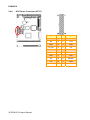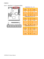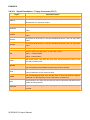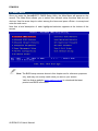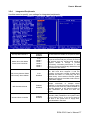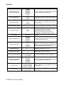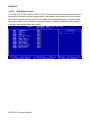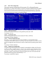
1
ECM-5510 5.25" AMD Geode GX466 333 MHz Mini Module with 128 MB DDR SDRAM Onboard, VGA, LVDS, Audio, LAN, CF, PC/104, PCI, 4 COM, 4 USB 1.1 & GPIO User’s Manual 2nd Ed – 19 January 2007 Part No. E2047551001R ECM-5510 FCC Statement THIS DEVICE COMPLIES WITH PART 15 FCC RULES. OPERATION IS SUBJECT TO THE FOLLOWING TWO CONDITIONS: (1) THIS DEVICE MAY NOT CAUSE HARMFUL INTERFERENCE. (2) THIS DEVICE MUST ACCEPT ANY INTERFERENCE RECEIVED INCLUDING INTERFERENCE THAT MAY CAUSE UNDESIRED OPERATION. THIS EQUIPMENT HAS BEEN TESTED AND FOUND TO COMPLY WITH THE LIMITS FOR A CLASS "A" DIGITAL DEVICE, PURSUANT TO PART 15 OF THE FCC RULES. THESE LIMITS ARE DESIGNED TO PROVIDE REASONABLE PROTECTION AGAINST HARMFUL INTERFERENCE WHEN THE EQUIPMENT IS OPERATED IN A COMMERCIAL ENVIRONMENT. THIS EQUIPMENT GENERATES, USES, AND CAN RADIATE RADIO FREQUENCY ENERGY AND, IF NOT INSTATLLED AND USED IN ACCORDANCE WITH THE INSTRUCTION MANUAL, MAY CAUSE HARMFUL INTERFERENCE TO RADIO COMMUNICATIONS. OPERATION OF THIS EQUIPMENT IN A RESIDENTIAL AREA IS LIKELY TO CAUSE HARMFUL INTERFERENCE IN WHICH CASE THE USER WILL BE REQUIRED TO CORRECT THE INTERFERENCE AT HIS OWN EXPENSE. Notice This guide is designed for experienced users to setup the system within the shortest time. For detailed information, please always refer to the electronic user's manual. Copyright Notice Copyright © 2007 Avalue Technology Inc., ALL RIGHTS RESERVED. No part of this document may be reproduced, copied, translated, or transmitted in any form or by any means, electronic or mechanical, for any purpose, without the prior written permission of the original manufacturer. Trademark Acknowledgement Brand and product names are trademarks or registered trademarks of their respective owners. 2 ECM-5510 User’s Manual User’s Manual Disclaimer Avalue Technology Inc. reserves the right to make changes, without notice, to any product, including circuits and/or software described or contained in this manual in order to improve design and/or performance. Avalue Technology assumes no responsibility or liability for the use of the described product(s), conveys no license or title under any patent, copyright, or masks work rights to these products, and makes no representations or warranties that these products are free from patent, copyright, or mask work right infringement, unless otherwise specified. Applications that are described in this manual are for illustration purposes only. Avalue Technology Inc. makes no representation or warranty that such application will be suitable for the specified use without further testing or modification. Life Support Policy Avalue Technology’s PRODUCTS ARE NOT FOR USE AS CRITICAL COMPONENTS IN LIFE SUPPORT DEVICES OR SYSTEMS WITHOUT THE PRIOR WRITTEN APPROVAL OF Avalue Technology Inc. As used herein: 1. Life support devices or systems are devices or systems which, (a) are intended for surgical implant into body, or (b) support or sustain life and whose failure to perform, when properly used in accordance with instructions for use provided in the labeling, can be reasonably expected to result in significant injury to the user. 2. A critical component is any component of a life support device or system whose failure to perform can be reasonably expected to cause the failure of the life support device or system, or to affect its safety or effectiveness. A Message to the Customer Avalue Customer Services Each and every Avalue’s product is built to the most exacting specifications to ensure reliable performance in the harsh and demanding conditions typical of industrial environments. Whether your new Avalue device is destined for the laboratory or the factory floor, you can be assured that your product will provide the reliability and ease of operation for which the name Avalue has come to be known. Your satisfaction is our primary concern. Here is a guide to Avalue’s customer services. To ensure you get the full benefit of our services, please follow the instructions below carefully. ECM-5510 User’s Manual 3 ECM-5510 Technical Support We want you to get the maximum performance from your products. So if you run into technical difficulties, we are here to help. For the most frequently asked questions, you can easily find answers in your product documentation. These answers are normally a lot more detailed than the ones we can give over the phone. So please consult the user’s manual first. To receive the latest version of the user’s manual; please visit our Web site at: http://www.avalue.com.tw/ If you still cannot find the answer, gather all the information or questions that apply to your problem, and with the product close at hand, call your dealer. Our dealers are well trained and ready to give you the support you need to get the most from your Avalue’s products. In fact, most problems reported are minor and are able to be easily solved over the phone. In addition, free technical support is available from Avalue’s engineers every business day. We are always ready to give advice on application requirements or specific information on the installation and operation of any of our products. Please do not hesitate to call or e-mail us. Headquarters Avalue Technology Inc. 7F, 228, Lian-cheng Road, Chung Ho City, Taipei, Taiwan Tel : +886-2-8226-2345 Fax : +886-2-8226-2777 http://www.avalue.com.tw E-mail: [email protected] Europe Branch Office Avalue Europe A/S Nordre Strandvej 13, 3480 Fredensborg, Denmark Tel : +45-7025-0310 Fax : +45-4975-5026 http://www.avalue.com.tw E-mail: [email protected] China Branch Office Avalue Technology Shanghai Inc. Room 909, 9F, Section B, No.900, Yisan Road, Caohejing Hi-tech Park, Shanghai 200233, China Tel : +86-21-5423-4170 Fax : +86-21-5423-4171 http://www.avalue.com.tw E-mail: [email protected] US Branch Office Avalue Technology Inc. Suite 210, 200 Tornillo Way, Tinton Falls, NJ 07712 USA Tel: +1-732-578-0200 Fax: +1-732-578-0250 http://www.avalue.com.tw E-mail: [email protected] 4 ECM-5510 User’s Manual User’s Manual Product Warranty Avalue warrants to you, the original purchaser, that each of its products will be free from defects in materials and workmanship for two years from the date of purchase. This warranty does not apply to any products which have been repaired or altered by persons other than repair personnel authorized by Avalue, or which have been subject to misuse, abuse, accident or improper installation. Avalue assumes no liability under the terms of this warranty as a consequence of such events. Because of Avalue’s high quality-control standards and rigorous testing, most of our customers never need to use our repair service. If any of Avalue’s products is defective, it will be repaired or replaced at no charge during the warranty period. For out-of-warranty repairs, you will be billed according to the cost of replacement materials, service time, and freight. Please consult your dealer for more details. If you think you have a defective product, follow these steps: 1. Collect all the information about the problem encountered. (For example, CPU type and speed, Avalue’s products model name, hardware & BIOS revision number, other hardware and software used, etc.) Note anything abnormal and list any on-screen messages you get when the problem occurs. 2. Call your dealer and describe the problem. Please have your manual, product, and any helpful information available. 3. If your product is diagnosed as defective, obtain an RMA (return material authorization) number from your dealer. This allows us to process your good return more quickly. 4. Carefully pack the defective product, a complete Repair and Replacement Order Card and a photocopy proof of purchase date (such as your sales receipt) in a shippable container. A product returned without proof of the purchase date is not eligible for warranty service. 5. Write the RMA number visibly on the outside of the package and ship it prepaid to your dealer. ECM-5510 User’s Manual 5 ECM-5510 Contents 1. Getting Started..........................................................................................................10 1.1 Safety Precautions ..................................................................................................10 1.2 Packing List.............................................................................................................10 1.3 Document Amendment History ...............................................................................11 1.4 Manual Objectives...................................................................................................12 1.5 System Specifications .............................................................................................13 1.6 Architecture Overview .............................................................................................15 1.6.1 Block Diagram ................................................................................................................................ 15 1.6.2 AMD Geode GX2 & CS5535.......................................................................................................... 16 1.6.3 VIA VT1612A Audio Codec............................................................................................................ 18 1.6.4 Ethernet.......................................................................................................................................... 18 1.6.5 Winbond W83627HF-AW LPC Super I/O ...................................................................................... 19 1.6.6 Winbond W83977EF ISA Super I/O............................................................................................... 19 1.6.7 NS DS90C385 LVDS Transmitter .................................................................................................. 20 1.6.8 ITE IT8888F PCI-ISA Bridge.......................................................................................................... 20 2. Hardware Configuration...........................................................................................21 2.1 Product Overview....................................................................................................22 2.2 Installation Procedure .............................................................................................23 2.2.1 2.3 2.4 Main Memory.................................................................................................................................. 24 Jumper and Connector List .....................................................................................26 Setting Jumpers & Connectors ...............................................................................28 2.4.1 BIOS Write Protect Select (JP1) .................................................................................................... 28 2.4.2 TFT/CRT Select (JP2).................................................................................................................... 28 2.4.3 Clear CMOS (JP3) ......................................................................................................................... 29 2.4.4 COM2 RS-232/422/485 Select (JP5, JP6)..................................................................................... 29 2.4.5 COM2/4/3/1 Pin 9 Select (JP7, JP8, JP9, JP10) ........................................................................... 30 2.4.6 LCD Inverter Power Select (JP11) ................................................................................................. 30 2.4.7 Compact Flash Mode Select (JP13) .............................................................................................. 31 2.4.8 DOC Memory Address Select (JP14) ............................................................................................ 31 2.4.9 ATX Power Connector (ATX1) ....................................................................................................... 32 2.4.10 System Fan Connector (CN1).................................................................................................... 33 2.4.11 CPU Fan Connector (CN2) ........................................................................................................ 33 2.4.12 TFT Panel Connector (CN3) ...................................................................................................... 34 2.4.13 LVDS Connector (CN4) ............................................................................................................. 36 2.4.14 CD-ROM Audio Input Connector (CN5)..................................................................................... 37 2.4.15 Serial Port 1, 3, 4 Connector (CN6)........................................................................................... 38 6 ECM-5510 User’s Manual User’s Manual 2.4.16 Serial Port 2 Connector in RS-232 Mode (CN6, Pin 11-20) ...................................................... 40 2.4.17 Serial Port 2 Connector in RS-422 Mode (CN6, Pin 11-20) ...................................................... 41 2.4.18 Serial Port 2 Connector in RS-485 Mode (CN6, Pin 11-20) ...................................................... 42 2.4.19 PC/104 Connector (CN7 + CN8) ............................................................................................... 43 2.4.20 IrDA Connector (CN10).............................................................................................................. 49 2.4.21 Keyboard & Mouse Connector (CN11) ...................................................................................... 50 2.4.22 USB Connector 0, 1, 2 & 3 (CN12, CN15)................................................................................. 51 2.4.23 LCD Inverter Connector (CN13) ................................................................................................ 52 2.4.24 Primary IDE Connector (CN14) ................................................................................................. 53 2.4.25 Floppy Connector (FLP1)........................................................................................................... 55 2.4.26 Digital I/O Connector (JDIO1) .................................................................................................... 57 2.4.27 Front Panel Connector (JFP1) ................................................................................................... 58 2.4.28 Audio Connector (JP4)............................................................................................................... 59 2.4.29 LCD Backlight Brightness Adjustment Connector (JP12).......................................................... 60 2.4.30 -5V/-12V PC/104 Voltage Connector (JP15) ............................................................................. 60 2.4.31 Parallel Port Connector (LPT1).................................................................................................. 61 2.4.32 Power Connector (PWR1) ......................................................................................................... 62 2.4.33 VGA Connector (VGA1)............................................................................................................. 63 3 BIOS Setup................................................................................................................64 3.1 Starting Setup .........................................................................................................65 3.2 3.3 3.4 3.5 Using Setup ............................................................................................................66 Getting Help ............................................................................................................67 In Case of Problems................................................................................................67 Main Menu ..............................................................................................................68 3.5.1 Standard CMOS Features.............................................................................................................. 69 3.5.2 Advanced BIOS Features .............................................................................................................. 71 3.5.3 Advanced Chipset Features........................................................................................................... 75 3.5.4 Integrated Peripherals .................................................................................................................... 77 3.5.5 Power Management Setup............................................................................................................. 79 3.5.6 PnP / PCI Configuration ................................................................................................................. 81 3.5.7 PC Health Status............................................................................................................................ 82 3.5.8 Load Fail-Safe Defaults.................................................................................................................. 83 3.5.9 Load Optimized Defaults ................................................................................................................ 83 3.5.10 Set Supervisor / User Password................................................................................................ 84 3.5.11 Save & Exit Setup ...................................................................................................................... 85 3.5.12 Exit Without Save....................................................................................................................... 86 ECM-5510 User’s Manual 7 ECM-5510 4 Drivers Installation ...................................................................................................87 4.1 Install Audio Driver (For AMD GX2) ........................................................................88 4.2 Install Display Driver (For AMD GX2)......................................................................90 4.3 Install Ethernet Driver (For Realtek RTL810x, RTL813x Family) ............................92 5 Measurement Drawing .............................................................................................93 Appendix A: BIOS Revisions ..........................................................................................95 Appendix B: AWARD BIOS POST Messages ................................................................96 Overview............................................................................................................................97 Post Beep ..........................................................................................................................97 Error Messages .................................................................................................................97 1. CMOS BATTERY HAS FAILED ......................................................................................................... 97 2. CMOS CHECKSUM ERROR ............................................................................................................. 97 3. DISK BOOT FAILURE, INSERT SYSTEM DISK AND PRESS ENTER ............................................ 97 4. DISKETTE DRIVES OR TYPES MISMATCH ERROR - RUN SETUP.............................................. 97 5. DISPLAY SWITCH IS SET INCORRECTLY...................................................................................... 98 6. DISPLAY TYPE HAS CHANGED SINCE LAST BOOT ..................................................................... 98 7. EISA Configuration Checksum Error PLEASE RUN EISA CONFIGURATION UTILITY................... 98 8. EISA Configuration Is Not Complete PLEASE RUN EISA CONFIGURATION UTILITY ................... 98 9. ERROR ENCOUNTERED INITIALIZING HARD DRIVE.................................................................... 98 10. ERROR INITIALIZING HARD DISK CONTROLLER ..................................................................... 98 11. FLOPPY DISK CNTRLR ERROR OR NO CNTRLR PRESENT ................................................... 98 12. Invalid EISA Configuration PLEASE RUN EISA CONFIGURATION UTILITY .............................. 99 13. KEYBOARD ERROR OR NO KEYBOARD PRESENT ................................................................. 99 14. Memory Address Error at ... ........................................................................................................... 99 15. Memory parity Error at ................................................................................................................... 99 16. MEMORY SIZE HAS CHANGED SINCE LAST BOOT ................................................................. 99 17. Memory Verify Error at ... ............................................................................................................... 99 18. OFFENDING ADDRESS NOT FOUND ......................................................................................... 99 19. OFFENDING SEGMENT: .............................................................................................................. 99 20. PRESS A KEY TO REBOOT ....................................................................................................... 100 21. PRESS F1 TO DISABLE NMI, F2 TO REBOOT ......................................................................... 100 22. RAM PARITY ERROR - CHECKING FOR SEGMENT ... ........................................................... 100 23. Should Be Empty But EISA Board Found PLEASE RUN EISA CONFIGURATION UTILITY..... 100 24. Should Have EISA Board But Not Found PLEASE RUN EISA CONFIGURATION UTILITY ..... 100 25. Slot Not Empty ............................................................................................................................. 100 26. SYSTEM HALTED, (CTRL-ALT-DEL) TO REBOOT ... ............................................................... 100 27. Wrong Board In Slot PLEASE RUN EISA CONFIGURATION UTILITY...................................... 101 28. FLOPPY DISK(S) fail (80) → Unable to reset floppy subsystem................................................. 101 29. FLOPPY DISK(S) fail (40) → Floppy Type dismatch................................................................... 101 8 ECM-5510 User’s Manual User’s Manual 30. Hard Disk(s) fail (80) → HDD reset failed.................................................................................. 101 31. Hard Disk(s) fail (40) → HDD controller diagnostics failed........................................................ 101 32. Hard Disk(s) fail (20) → HDD initialization error........................................................................ 101 33. Hard Disk(s) fail (10) → Unable to recalibrate fixed disk........................................................... 101 34. Hard Disk(s) fail (08) → Sector Verify failed.............................................................................. 101 35. Keyboard is locked out - Unlock the key. ..................................................................................... 101 36. Keyboard error or no keyboard present. ...................................................................................... 101 37. Manufacturing POST loop............................................................................................................ 101 38. BIOS ROM checksum error - System halted. .............................................................................. 101 39. Memory test fail. ........................................................................................................................... 101 40. POST Codes ................................................................................................................................ 102 ECM-5510 User’s Manual 9 ECM-5510 1. Getting Started 1.1 Safety Precautions Warning! Always completely disconnect the power cord from your chassis whenever you work with the hardware. Do not make connections while the power is on. Sensitive electronic components can be damaged by sudden power surges. Only experienced electronics personnel should open the PC chassis. Caution! Always ground yourself to remove any static charge before touching the CPU card. Modern electronic devices are very sensitive to static electric charges. As a safety precaution, use a grounding wrist strap at all times. Place all electronic components in a static-dissipative surface or static-shielded bag when they are not in the chassis. 1.2 Packing List Before you begin installing your single board, please make sure that the following materials have been shipped: z 1 x ECM-5510 onboard AMD Geode GX466 333 MHz mini module z 1 x Quick Installation Guide for ECM-5510 z 1 x CD-ROM or DVD-ROM contains the followings: — — — — User’s Manual (this manual in PDF file) Ethernet driver and utilities VGA drivers and utilities Audio drivers and utilities 10 ECM-5510 User’s Manual User’s Manual 1.3 Document Amendment History Revision st 1 Date By May, 2006 Vicky Lin Comment Initial Release ECM-5510 User’s Manual 11 ECM-5510 1.4 Manual Objectives This manual describes in detail the Avalue Technology ECM-5510 Single Board. We have tried to include as much information as possible but we have not duplicated information that is provided in the standard IBM Technical References, unless it proved to be necessary to aid in the understanding of this board. We strongly recommend that you study this manual carefully before attempting to interface with ECM-5510 series or change the standard configurations. Whilst all the necessary information is available in this manual we would recommend that unless you are confident, you contact your supplier for guidance. Please be aware that it is possible to create configurations within the CMOS RAM that make booting impossible. If this should happen, clear the CMOS settings, (see the description of the Jumper Settings for details). If you have any suggestions or find any errors concerning this manual and want to inform us of these, please contact our Customer Service department with the relevant details. 12 ECM-5510 User’s Manual User’s Manual 1.5 System Specifications System Onboard AMD Geode GX466 333 MHz CPU Note: Available in different CPU speeds by request BIOS Award 512 KB Flash BIOS System Chipset AMD Geode GX466/CS5535 I/O Chip Winbond W83627HF-AW 64/128/256 MB DDR SDRAM onboard System Memory One 184-pin DIMM socket supports up to 512 MB DDR 200/266 SDRAM SSD One M-Systems DiskOnChip, one CompactFlash Type I/II socket Watchdog Timer Reset: 1 sec.~255 min. and 1 sec. or 1 min./step Expansion One PC/104 connector, one PCI slot (PCI Rev. 2.2 compliant) I/O 2 x EIDE (Ultra DMA 66), 1 x FDD, 1 x LPT, 3 x RS-232, MIO 1 x RS-232/422/482, 1 x K/B, 1 x Mouse IrDA 115k bps, IrDA 1.0 compliant USB 4 x USB 1.1 ports DIO 16-bit General Purpose I/O for DI and DO Display Chipset AMD Geode GX466 with integrated 2D graphics engine Display Memory 8/16 MB frame buffer using system memory CRT mode: 1280 x 1024 @ 24 bpp (60 Hz) Resolution LCD mode: 1280 x 1024 @ 24 bpp (85 Hz) PCI bus VGA/LCD interface VGA/LCD Interface LVDS Supports 18/24-bit TFT panels Single channel 24-bit LVDS Audio Chipset AMD Geode CS5535 AC97 Codec VIA VT1612A Audio Interface Mic in, Line in, CD Audio in, Line out Ethernet Realtek RTL8100C LAN 1 Ethernet Interface Optional Intel® 82551QM/82551ER 100Base-Tx Fast Ethernet compatible ECM-5510 User’s Manual 13 ECM-5510 Mechanical & Environmental +5V @ 1.71 A, 5 Vsb @ 0.17 A (with AMD Geode GX466 333 MHz & 256 Power Requirement MB DDR SDRAM) Power Type AT/ATX Operation Temperature 0~60oC (32~140o F) Operating Humidity 0%~90% relative humidity, non-condensing Size ( L x W ) 8" x 5.75" (203 mm x 146 mm) Weight 0.88 lbs (0.4 Kg) 14 ECM-5510 User’s Manual User’s Manual 1.6 Architecture Overview 1.6.1 Block Diagram The following block diagram shows the architecture and main components of ECM-5510. The following sections provide detail information about the functions provided onboard. ECM-5510 User’s Manual 15 ECM-5510 1.6.2 AMD Geode GX2 & CS5535 The AMD Geode GX2 processor is designed from the ground-up for information appliances, the GX2 processor delivers optimal performance for full-featured multimedia applications across broadband connections. The GX2 processor includes a powerful 32-bit-x86 core integrated FPU, a display controller with up to 1600 x 1200 resolution, a graphic processor, a SDRAM controller (SDR or DDR supported), a TFT interface and integrated DACs for CRT support (pinout options). Together with its AMD Geode CS5535 I/O companion device, the AMD Geode GX2 processor delivers the optimum balance between power consumption and performance. The GX2 processor is powered by a new x86 core with support for MMX and 3DNow! extensions. Built around AMD’s GeodeLink architecture with an on-chip bandwidth of up to 6 Gbps, the GX2 processor supports high quality multimedia applications. The AMD Geode GX2 processor is a very low powered x86 microprocessor with typical power consumption of less than 1.5 W. It’s a highly integrated solution that enables small form factor devices. Outstanding features: • 32-bit low-power x86 processor with support for Intel MMX and 3DNow! extensions • 32 KB of level 1 cache,16 KB instruction, and 16 KB data • High-performance patented GeodeLink architecture Integrated display controller • Integrated video DACs and integrated TFT interface for flexible output options: CRT or TFT (Bond-out option) • PCI 66 MHz Bus Industry standard PCI 2.2 specification compliant Write gathering and write posting of inbound write requests Supports fast back to back transactions • 64-bit SDR or DDR memory controller with integrated graphics • Integrated thermal diode • Optimized Unified Memory Architecture (UMA) with patented compression technology • EBGA-368 terminal package Memory controller • Integrated memory controller for low latency to CPU and on-chip peripherals • 64-bit wide SDRAM bus Graphics processor • High performance 2D graphics controller • Alpha BLT • Integrated dot clock PLL • 16 ECM-5510 User’s Manual User’s Manual Display controller Supports up to 1600 x 1200 x 16 BPP and 1280 x 1024 x 24 BPP @ 85 Hz (CRT) • Hardware-based VGA • Hardware video up/down scaler • Graphics/video alpha blending • TFT or CRT interface • Integrated CRT DACs IDE controller • UDMA-66 compliant • One channel with two devices Flash interface • Multiplexed with IDE interface • Connects to an array of industry standard NAND Flash and/or NOR Flash USB controllers • 2 USB 1.1 controllers, supporting total of four ports Audio codec 97 controller • AC97 specification version 2.1 compliant interface to multiple audio codecs: serial in, serial-out, bit clock-in • Multiple codec support • Surround sound support IR (infrared) communication port • Shared with serial port 1 • 16550A and 16450 software compatible • Consumer-IR (TV-remote) mode • HP-SIR • Selectable internal or external modulation/demodulation (SHARP-IR) • Consumer remote control supports RC-5, RC-6, NEC, RCA, • RECS 80 AMD Geode Solutions CS5535 companion device – • GX2 Processor System Management Bus (SMB) controller • Compatible with Intel System Management Bus, Phillips I2C, and ACCESS.bus LPC (low pin count) port • Based on Intel LPC interface specifications, revision 1.0 General Purpose I/Os (GPIOs) • Up to 28 programmable GPIOs: in, out, I/O, open-drain, pull-up/down, and invert • ECM-5510 User’s Manual 17 ECM-5510 1.6.3 VIA VT1612A Audio Codec VIA Technologies’ VT1612ATM 18-bit audio codec conforms to the AC’97 2.2. The VT1612A integrates Sample Rate Converters and can be adjusted in 1Hz increments. The analog mixer circuitry integrates a stereo enhancement to provide a pleasing 3D surround sound effect for stereo media. Furthermore, an integrated headphone amplifier with thermal shutdown adds signal value by reducing the BOM. This codec is designed with aggressive power management to achieve low power consumption. When used with 3.3V analog supply, power consumption is further reduced. The primary applications for this part are desktop and portable personal computers multimedia subsystems. 1.6.4 Ethernet 1.6.4.1 Realtek RTL8100C Ethernet Controller The Realtek RTL8100C(L) is enhanced with an ACPI (Advanced Configuration Power Interface) management function for PCI in order to provide efficient power management for advanced operating systems with OSPM (Operating System Directed Power Management). It also supports remote wake-up (including AMD Magic Packet™ and Microsoft® Wake-up frame) to increase cost-efficiency in network maintenance and management. • 128-pin PQFP/LQFP (PQFP package pin-to-pin compatible with Realtek RTL8110S-32 Single-Chip Gigabit Ethernet Controller) • Supports PCI/mini-PCI interfaces • Integrates Fast Ethernet MAC, physical chip, and transceiver onto a single chip • 10Mbps and 100Mbps operation supporting N-way auto-negotiation • Supports 25MHz Crystal or 25MHz OSC as the internal clock source • Complies with PC99/PC2001 standards • Supports ACPI power management • Provides PCI bus master data transfer • Provides PCI memory space or I/O space mapped data transfer • Supports PCI clock speed of 16.75MHz-40MHz • Advanced power saving mode • Supports Wake-on-LAN and remote wake-up (AMD Magic Packet™, Link Change, and Microsoft® Wake-up frame) • Half/Full duplex capability • Supports Full Duplex Flow Control (IEEE 802.3x) • Provides interface to 93C46 EEPROM to store resource configuration and ID parameters • Provides PCI clock run pin • Provides LED pins for network operation status indication • 2.5/3.3V power supply with 5V tolerant I/Os • 0.25µm CMOS process 18 ECM-5510 User’s Manual User’s Manual 1.6.5 Winbond W83627HF-AW LPC Super I/O The Winbond W83627F/HF is made to fully comply with Microsoft PC98 and PC99 Hardware Design Guide. Moreover, W83627F/HF is made to meet the specification of PC98/PC99’s requirement in the power management: ACPI and DPM (Device Power Management). Super I/O chip provides features as the following: • Meet LPC Spec. 1.0 • Support LDRQ# (LPC DMA), SERIRQ (serial IRQ) • Include all features of Winbond I/O W83977TF and W83977EF • Integrate Hardware Monitor functions • Compliant with Microsoft PC98/PC99 Hardware Design Guide. • Support DPM (Device Power Management), ACPI • Programmable configuration settings • Single 24 or 48 MHz clock input 1.6.6 Winbond W83977EF ISA Super I/O The Winbond W83627F/HF is made to fully comply with Microsoft PC98 Hardware Design Guide. Moreover, W83627F/HF is made to meet the specification of PC98’s requirement in the power management: ACPI and DPM (Device Power Management). Super I/O chip provides features as the following: • • • • • • Plug & Play 1.0A compatible Supports 12 IRQs, 4 DMA channels, full 16-bit address decoding Capable of ISA Bus IRQ Sharing Compliant with Microsoft PC98 Hardware Design Guide Supports DPM (Device Power Management), ACPI Reports ACPI status interrupt by SCI# signal issued from any of the 12 IRQs pins or GPIO xx • Programmable configuration settings • Single 24/48 Mhz clock input ECM-5510 User’s Manual 19 ECM-5510 1.6.7 NS DS90C385 LVDS Transmitter The DS90C385 transmitter converts 28 bits of LVCMOS/LVTTL data into four LVDS (Low Voltage Differential Signaling) data streams. A phase-locked transmit clock is transmitted in parallel with the data streams over a fifth LVDS link. Every cycle of the transmit clock 28 bits of input data are sampled and transmitted. At a transmit clock frequency of 85 MHz, 24 bits of RGB data and 3 bits of LCD timing and control data (FPLINE, FPFRAME, DRDY) are transmitted at a rate of 595 Mbps per LVDS data channel. Using a 85 MHz clock, the data throughput is 297.5 Mbytes/sec. Also available is the DS90C365 that converts 21 bits of LVCMOS/LVTTL data into three LVDS (Low Voltage Differential Signaling) data streams. Both transmitters can be programmed for Rising edge strobe or Falling edge strobe through a dedicated pin. A Rising edge or Falling edge strobe transmitter will interoperate with a Falling edge strobe Receiver (DS90CF386/DS90CF366) without any translation logic. 1.6.8 ITE IT8888F PCI-ISA Bridge The IT8888F is a PCI to ISA bridge single function device. The IT8888F serves as a bridge between the PCI bus and ISA bus. The IT8888F’s 32-bit PCI bus interface is compliant with PCI Specification V2.1 and supports both PCI Bus Master & Slave. 20 ECM-5510 User’s Manual User’s Manual 2. Hardware Configuration ECM-5510 User’s Manual 21 ECM-5510 2.1 Product Overview 22 ECM-5510 User’s Manual User’s Manual 2.2 Installation Procedure This chapter explains you the instructions of how to setup your system. 1. Turn off the power supply. 2. Insert the DIMM module (be careful with the orientation). 3. Insert all external cables for hard disk, floppy, keyboard, mouse, USB etc. except for flat panel. A CRT monitor must be connected in order to change CMOS settings to support flat panel. 4. Connect power supply to the board via the ATXPWR. 5. Turn on the power. 6. Enter the BIOS setup by pressing the delete key during boot up. Use the “LOAD BIOS DEFAULTS” feature. The Integrated Peripheral Setup and the Standard CMOS Setup Window must be entered and configured correctly to match the particular system configuration. 7. If TFT panel display is to be utilized, make sure the panel voltage is correctly set before connecting the display cable and turning on the power. ECM-5510 User’s Manual 23 ECM-5510 2.2.1 Main Memory ECM-5510 provides one 184-pin SODIMM sockets to support DDR SDRAM. The total maximum memory size is 512 MB. DIMM1 Make sure to unplug the power supply before adding or removing DIMMs or other system components. Failure to do so may cause severe damage to both the board and the components. 24 ECM-5510 User’s Manual User’s Manual • • • • Locate the DIMM slot on the board. Hold two edges of the DIMM module carefully. Keep away of touching its connectors. Align the notch key on the module with the rib on the slot. Firmly press the modules into the slot automatically snaps into the mounting notch. Do not force the DIMM module in with extra force as the DIMM module only fit in one direction. • To remove the DIMM modules, push the two ejector tabs on the slot outward simultaneously, and then pull out the DIMM module. Note: (1) Please do not change any DDR SDRAM parameter in BIOS setup to increase your system’s performance without acquiring technical information in advance. (2) Static electricity can damage the electronic components of the computer or optional boards. Before starting these procedures, ensure that you are discharged of static electricity by touching a grounded metal object briefly. ECM-5510 User’s Manual 25 ECM-5510 2.3 Jumper and Connector List You can configure your board to match the needs of your application by setting jumpers. A jumper is the simplest kind of electric switch. It consists of two metal pins and a small metal clip (often protected by a plastic cover) that slides over the pins to connect them. To “close” a jumper you connect the pins with the clip. To “open” a jumper you remove the clip. Sometimes a jumper will have three pins, labeled 1, 2, and 3. In this case, you would connect either two pins. The jumper settings are schematically depicted in this manual as follows: A pair of needle-nose pliers may be helpful when working with jumpers. Connectors on the board are linked to external devices such as hard disk drives, a keyboard, or floppy drives. In addition, the board has a number of jumpers that allow you to configure your system to suit your application. If you have any doubts about the best hardware configuration for your application, contact your local distributor or sales representative before you make any changes. The following tables list the function of each of the board's jumpers and connectors. Jumpers Label Function Note JP1 BIOS write protect select 3 x 1 header, pitch 2.54mm JP2 TFT/CRT select 2 x 1 header, pitch 2.0mm JP3 Clear CMOS 3 x 1 header, pitch 2.54mm JP5 JP6 COM2 RS-232/422/485 select 3 x 2 header, pitch 2.0mm 4 x 3 header, pitch 2.0mm JP7, JP8, JP9, JP10 COM 2/4/3/1 pin 9 select 3 x 2 header, pitch 2.0mm JP11 LCD inverter power select 3 x 1 header, pitch 2.0mm JP13 Compact Flash mode select 2 x 1 header, pitch 2.54mm JP14 DOC memory address select 2 x 1 header, pitch 2.0mm 26 ECM-5510 User’s Manual User’s Manual Connectors Label Function Note ATX1 ATX power connector CN1 System fan connector 3 x 1 wafer, pitch 2.54mm CN2 CPU fan connector 3 x 1 wafer, pitch 2.54mm CN3 TFT panel connector HIROSE DF13-40DP-1.25V CN4 LVDS connector HIROSE DF13-40DP-1.25V CN5 CD-ROM audio input connector 5 x 1 wafer, pitch 2.0mm CN6 Serial port 1, 2, 3, 4 connector 20 x 2 header, pitch 2.54mm CN7 + CN8 PC/104 connector CN9 Reserved CN10 IrDA connector 5 x 1 header, pitch 2.54mm CN11 Keyboard & mouse connector 4 x 2 header, pitch 2.54mm CN12 USB connector 0 & 1 5 x 2 header, pitch 2.54mm CN13 LCD inverter connector 5 x 1 wafer, pitch 2.0mm CN14 Primary IDE connector 20 x 2 header, pitch 2.54mm CN15 USB connector 2 & 3 5 x 2 header, pitch 2.54mm DIMM1 184-pin DIMM socket FLP1 Floppy connector 17 x 2 header, pitch 2.54mm JDIO1 Digital I/O connector 10 x 2 header, pitch 2.54mm JFP1 Front panel connector 8 x 2 header, pitch 2.54mm JP4 Audio connector 8 x 2 header, pitch 2.54mm JP12 LCD backlight brightness adjustment connector 3 x 1 header, pitch 2.0mm JP15 -5V/-12V PC/104 voltage connector 2 x 1 wafer, pitch 2.0mm LAN1 RJ-45 Ethernet LPT1 Parallel port connector PCI1 PCI slot PWR1 Power connector SN1 Compact Flash card connector U19 DiskOnChip socket VGA1 VGA connector 13 x 2 header, pitch 2.54mm 8 x 2 header, pitch 2.54mm ECM-5510 User’s Manual 27 ECM-5510 2.4 Setting Jumpers & Connectors 2.4.1 BIOS Write Protect Select (JP1) Protect* Write * Default 2.4.2 TFT/CRT Select (JP2) TFT CRT* * Default 28 ECM-5510 User’s Manual User’s Manual 2.4.3 Clear CMOS (JP3) Protect* Clear CMOS * Default 2.4.4 COM2 RS-232/422/485 Select (JP5, JP6) JP6 (JP5) (JP6) RS-232* RS-232* RS-422 RS-422 RS-485 RS-485 JP5 * Default ECM-5510 User’s Manual 29 ECM-5510 2.4.5 COM2/4/3/1 Pin 9 Select (JP7, JP8, JP9, JP10) +5V JP10 JP9 JP8 JP7 +12V Ring* * Default 2.4.6 LCD Inverter Power Select (JP11) +12V* +5V * Default 30 ECM-5510 User’s Manual User’s Manual 2.4.7 Compact Flash Mode Select (JP13) Master Slave* * Default 2.4.8 DOC Memory Address Select (JP14) D0000 D4000* D8000 Disabled * Default ECM-5510 User’s Manual 31 ECM-5510 2.4.9 ATX Power Connector (ATX1) 32 ECM-5510 User’s Manual Signal PIN PIN Signal NC 11 1 +3.3V NC 12 2 +3.3V GND 13 3 GND PS_ON 14 4 +5V GND 15 5 GND GND 16 6 +5V GND 17 7 GND NC 18 8 PWROK +5V 19 9 5VSB +5V 20 10 +12V User’s Manual 2.4.10 System Fan Connector (CN1) Signal PIN GND 1 +12V 2 TAC 3 2.4.10.1 Signal Description – System Fan Connector (CN1) Signal TAC 2.4.11 Signal Description Fan speed monitor CPU Fan Connector (CN2) Signal PIN GND 1 +12V 2 TAC 3 2.4.11.1 Signal Description – CPU Fan Connector (CN2) Signal TAC Signal Description Fan speed monitor ECM-5510 User’s Manual 33 ECM-5510 2.4.12 TFT Panel Connector (CN3) Signal PIN PIN Signal ENBLK 39 40 NC M 37 38 LP SHFCLK 35 36 FLM GND 33 34 GND P22 31 32 P23 P20 29 30 P21 P18 27 28 P19 P16 25 26 P17 P14 23 24 P15 P12 21 22 P13 P10 19 20 P11 P8 17 18 P9 P6 15 16 P7 P4 13 14 P5 P2 11 12 P3 P0 9 10 P1 VCON 7 8 GND +3.3V 5 6 +3.3V GND 3 4 GND +5V 1 2 +5V 2.4.12.1 Signal Description – TFT Panel Connecter (CN3) Signal Description P [0:23] Flat panel data output for 18/24 bit TFT flat panels. Refer to table below for configurations for various panel types. The flat panel data and control outputs are all on-board controlled for secure power-on/off sequencing SHFCLK Shift Clock. Pixel clock for flat panel data LP Flat panel equivalent of HSYNC (horizontal synchronization) FLM Flat panel equivalent of VSYNC (vertical synchronization) M Multipurpose signal, function depends on panel type. May be used as AC drive control signal or as BLANK# or Display Enable signal ENBKL Enable backlight signal. This signal is controlled as a part of the panel power sequencing ENVEE Enable VEE. Signal to control the panel power-on/off sequencing. A high level may turn on the VEE (LCD bias voltage) supply to the panel 34 ECM-5510 User’s Manual User’s Manual 2.4.12.2 Signal Configuration – TFT Panel Display (CN3) Signal 18-bit TFT 24-bit TFT P0 - B0 P1 - B1 P2 B0 B2 P3 B1 B3 P4 B2 B4 P5 B3 B5 P6 B4 B6 P7 B5 B7 P8 - G0 P9 - G1 P10 G0 G2 P11 G1 G3 P12 G2 G4 P13 G3 G5 P14 G4 G6 P15 G5 G7 P16 - R0 P17 - R1 P18 R0 R2 P19 R1 R3 P20 R2 R4 P21 R3 R5 P22 R4 R6 P23 R5 R7 ECM-5510 User’s Manual 35 ECM-5510 2.4.13 LVDS Connector (CN4) Signal PIN PIN Signal NC 39 40 NC GND 37 38 GND NC 35 36 Txclk# NC 33 34 Txclk GND 31 32 GND NC 29 30 NC NC 27 28 NC GND 25 26 GND NC 23 24 NC NC 21 22 NC GND 19 20 GND Txout3# 17 18 Txout2# Txout3 15 16 Txout2 GND 13 14 GND Txout1# 11 12 Txout0# Txout1 9 10 Txout0 GND 7 8 2 GND 2 I C_CLK 5 6 I C_DAT +3.3V 3 4 +5V +3.3V 1 2 +5V 2.4.13.1 Signal Description – LVDS Connecter (CN4) Signal Description 2 I2C_DAT, I2C_CLK I C interface for panel parameter EEPROM. This EERPOM is mounted on the LVDS receiver. The data in the EEPROM allows the EXT module to automatically set the proper timing parameters for a specific LCD panel. 36 ECM-5510 User’s Manual User’s Manual 2.4.14 CD-ROM Audio Input Connector (CN5) Signal PIN CD_R 4 GND 3 CD_L 2 GND 1 2.4.14.1 Signal Description – CD-ROM Audio Input Connecter (CN5) Signal Signal Description CD_R Right CD-IN signal CD_L Left CD-IN signal ECM-5510 User’s Manual 37 ECM-5510 2.4.15 Serial Port 1, 3, 4 Connector (CN6) Serial Port 1 (Pin 1-10) Signal PIN PIN Signal DCD1 1 2 DSR1 RxD1 3 4 RTS1 TxD1 5 6 CTS1 DTR1 7 8 RI1/+5V/+12V GND 9 10 NC Serial Port 3 (Pin 21-30) Signal PIN PIN Signal DCD3 21 22 DSR3 RxD3 23 24 RTS3 TxD3 25 26 CTS3 DTR3 27 28 RI3/+5V/+12V GND 29 30 NC Serial Port 4 (Pin 31-40) 38 ECM-5510 User’s Manual Signal PIN PIN Signal DCD4 31 32 DSR4 RxD4 33 34 RTS4 TxD4 35 36 CTS4 DTR4 37 38 RI4/+5V/+12V GND 39 40 NC User’s Manual 2.4.15.1 Signal Description – Serial Port 1, 3, 4 Connector (CN6) Signal Signal Description Serial output. This signal sends serial data to the communication link. The signal is TxD set to a marking state on hardware reset when the transmitter is empty or when loop mode operation is initiated. RxD DTR DSR RTS CTS DCD RI Serial input. This signal receives serial data from the communication link. Data Terminal Ready. This signal indicates to the modem or data set that the on-board UART is ready to establish a communication link. Data Set Ready. This signal indicates that the modem or data set is ready to establish a communication link. Request To Send. This signal indicates to the modem or data set that the on-board UART is ready to exchange data. Clear To Send. This signal indicates that the modem or data set is ready to exchange data. Data Carrier Detect. This signal indicates that the modem or data set has detected the data carrier. Ring Indicator. This signal indicates that the modem has received a telephone ringing signal. ECM-5510 User’s Manual 39 ECM-5510 2.4.16 Serial Port 2 Connector in RS-232 Mode (CN6, Pin 11-20) Signal PIN PIN Signal DCD2 11 12 DSR2 RxD2 13 14 RTS2 TxD2 15 16 CTS2 DTR2 17 18 RI2/+5V/+12V GND 19 20 NC 2.4.16.1 Signal Description – Serial Port 2 Connector in RS-232 Mode (CN6, Pin 11-20) Signal Signal Description Serial output. This signal sends serial data to the communication link. The signal is TxD set to a marking state on hardware reset when the transmitter is empty or when loop mode operation is initiated. RxD DTR DSR RTS CTS DCD RI Serial input. This signal receives serial data from the communication link. Data Terminal Ready. This signal indicates to the modem or data set that the on-board UART is ready to establish a communication link. Data Set Ready. This signal indicates that the modem or data set is ready to establish a communication link. Request To Send. This signal indicates to the modem or data set that the on-board UART is ready to exchange data. Clear To Send. This signal indicates that the modem or data set is ready to exchange data. Data Carrier Detect. This signal indicates that the modem or data set has detected the data carrier. Ring Indicator. This signal indicates that the modem has received a telephone ringing signal. 40 ECM-5510 User’s Manual User’s Manual 2.4.17 Serial Port 2 Connector in RS-422 Mode (CN6, Pin 11-20) Signal PIN PIN Signal TxD- 11 12 RxD+ TxD+ 13 14 RxD- GND 15 16 NC NC 17 18 NC NC 19 20 NC 2.4.17.1 Signal Description – Serial Port 2 Connector in RS-422 Mode (CN6, Pin 11-20) Signal Signal Description Serial output. This differential signal pair sends serial data to the communication TxD+/- link. Data is transferred from Serial Port 2 Transmit Buffer Register to the communication link, if the RTS register of the Serial Port 2 is set to LOW. Serial input. This differential signal pair receives serial data from the RxD+/- communication link. Received data is available in Serial Port 2 Receiver Buffer Register. ECM-5510 User’s Manual 41 ECM-5510 2.4.18 Serial Port 2 Connector in RS-485 Mode (CN6, Pin 11-20) Signal PIN PIN Signal DATA+ 11 12 NC DATA- 13 14 NC GND 15 16 NC NC 17 18 NC NC 19 20 NC 2.4.18.1 Signal Description – Serial Port 2 Connector in RS-485 Mode (CN6, Pin 11-20) Signal Signal Description This differential signal pair sends and receives serial data to the communication DATA+/- link. The mode of this differential signal pair is controlled through the RTS register of Serial Port 2. Set the RTS register of the Serial Port 2 to LOW for transmitting, HIGH for receiving. Do not select a mode different from the one used by the connected peripheral, as this may damage CPU board and/or peripheral. The transmitter drivers in the port are short circuit protected by a thermal protection circuit. The circuit disables the drivers when the die temperature reaches 150 °C. RS-422 mode is typically used in point to point communication. Data and control signal pairs should be terminated in the receiver end with a resistor matching the cable impedance (typical 100-120 Ω). The resistors could be placed in the connector housing. RS-485 mode is typically used in multi drop applications, where more than 2 units are communicating. The data and control signal pairs should be terminated in each end of the communication line with a resistor matching the cable impedance (typical 100-120 Ω). Stubs to substations should be avoided. 42 ECM-5510 User’s Manual User’s Manual 2.4.19 PC/104 Connector (CN7 + CN8) CN7 CN7 Signal PIN PIN Signal GND B32 A32 GND GND B31 A31 SA0 OSC B30 A30 SA1 +5V B29 A29 SA2 BALE B28 A28 SA3 TC B27 A27 SA4 DACK2# B26 A26 SA5 IRQ3 B25 A25 SA6 IRQ4 B24 A24 SA7 IRQ5 B23 A23 SA8 IRQ6 B22 A22 SA9 IRQ7 B21 A21 SA10 SYS_CLK B20 A20 SA11 REFRESH# B19 A19 SA12 DRQ1 B18 A18 SA13 DACK1# B17 A17 SA14 DRQ3 B16 A16 SA15 DACK3# B15 A15 SA16 IOR# B14 A14 SA17 IOW# B13 A13 SA18 SMEMR# B12 A12 SA19 SMEMW# B11 A11 AEN GND B10 A10 IOCHRDY +12V B9 A9 SD0 OWS# B8 A8 SD1 -12V B7 A7 SD2 DRQ2 B6 A6 SD3 -5V B5 A5 SD4 IRQ9 B4 A4 SD5 +5V B3 A3 SD6 RESETDRV B2 A2 SD7 GND B1 A1 IOCHK# ECM-5510 User’s Manual 43 ECM-5510 CN8 CN8 44 ECM-5510 User’s Manual Signal PIN PIN Signal NC C20 D20 GND SD15 C19 D19 GND SD14 C18 D18 MASTER# SD13 C17 D17 +5V SD12 C16 D16 DRQ7 SD11 C15 D15 DACK7# SD10 C14 D14 DRQ6 SD9 C13 D13 DACK6# SD8 C12 D12 DRQ5 MEMW# C11 D11 DACK5# MEMR# C10 D10 DRQ0 SA17 C9 D9 DACK0# SA18 C8 D8 IRQ14 SA19 C7 D7 IRQ15 LA20 C6 D6 IRQ12 LA21 C5 D5 IRQ11 LA22 C4 D4 IRQ10 LA23 C3 D3 IOCS16# SBHE# C2 D2 MEMCS16# GND C1 D1 GND User’s Manual 2.4.19.1 Signal Description – PC/104 Connector (CN7 + CN8) 2.4.19.1.1 Address Signal Signal Description The address signals LA [23:17] define the selection of a 128KB section of memory space within the 16MB address range of the 16-bit data bus. These signals are active high. The validity of the MEMCS16# depends on these signals only. These LA [17:23] address lines are presented to the system with tri-state drivers. The permanent master drives these lines except when an alternate master cycle occurs; in this case, the temporary master drives these lines. The LA signals are not defined for I/O accesses. SA [0:19] System address. Address lines for the first one Megabyte of memory. SA [9:0] used for I/O addresses. SA0 is the least significant bit This signal is an active low signal, that indicates that a byte is being transferred on SBHE# the upper byte (SD [15:8]) of the 16 bit bus. All bus masters will drive this line with a tri-state driver. 2.4.19.1.2 Data Signal Signal Description These signals are defined for the low order byte of the 16-bit data bus being the only bus for 8 bit PC-AT/PC104 adapter boards. Memory or I/O transfers on this part of the data bus are defined for 8-bit operations with even or odd addresses and for 16-bit operations for odd addresses only. The signals SA0 and SBHE# are used to define the data present on this bus: SD [0:7] SD [8:15] SBHE# SA0 SD8-SD15 SD0-SD7 Action 0 0 ODD EVEN Word transfer 0 1 ODD ODD 1 0 X EVEN 1 1 X ODD Byte transfer on SD8-SD15 Byte transfer on SD0-SD7 Byte transfer on SD7- These signals are defined for the high order byte of the 16-bit data bus. Memory or I/O transfers on this part of the bus are defined when SBHE# is active. ECM-5510 User’s Manual 45 ECM-5510 2.4.19.1.3 Commands Signal Signal Description This is an active high signal used to latch valid addresses from the current bus BALE master on the falling edge of BALE. During DMA, refresh and alternate master cycles, BALE is forced high for the duration of the transfer. BALE is driven by the permanent master with a totem-pole driver. This is an active low signal driven by the current master to indicate an I/O read operation. I/O mapped devices using this strobe for selection should decode IOR# addresses SA [15:0] and AEN. Additionally, DMA devices will use IOR# in conjunction with DACKn# to decode a DMA transfer from the I/O device. The current bus master will drive this line with a tri-state driver. This is an active low signal driven by the current master to indicate an I/O write operation. I/O mapped devices using this strobe for selection should decode IOW# addresses SA [15:0] and AEN. Additionally, DMA devices will use IOR# in conjunction with DACKn# to decode a DMA transfer from the I/O device. The current bus master will drive this line with a tri-state driver. This is an active low signal driven by the permanent master to indicate a memory read operation in the first 1MB of system memory. Memory mapped devices using SMEMR# this strobe should decode addresses SA [19:0] only. If an alternate master drives MEMR#, the permanent master will drive SMEMR# delayed by internal logic. The permanent master ties this line to VCC through a pull-up resistor to ensure that it is inactive during the exchange of bus masters. This is an active low signal driven by the permanent master to indicate a memory write operation in the first 1MB of system memory. Memory mapped devices using SMEMW# this strobe should decode addresses SA [19:0] only. If an alternate master drives MEMR#, the permanent master will drive SMEMR# delayed by internal logic. The permanent master ties this line to VCC through a pull-up resistor to ensure that it is inactive during the exchange of bus masters. This is an active low signal driven by the current master to indicate a memory read operation. Memory mapped devices using this strobe should decode addresses MEMR# LA [23:17] and SA [19:0]. All bus masters will drive this line with a tri-state driver. The permanent master ties this line to VCC through a pull-up resistor to ensure that it is inactive during the exchange of bus masters. This is an active low signal driven by the current master to indicate a memory write operation. Memory mapped devices using this strobe should decode addresses MEMW# LA [23:17] and SA [19:0]. All bus masters will drive this line with a tri-state driver. The permanent master ties this line to VCC through a pull-up resistor to ensure that it is inactive during the exchange of bus masters. 46 ECM-5510 User’s Manual User’s Manual 2.4.19.1.4 Transfer Response Signal Signal Description This is an active low signal driven by an I/O-mapped PC-AT/PC104 adapter IOCS16# indicating that the I/O device located at the address is a 16-bit device. This open collector signal is driven, based on SA [15:0] only (not IOR# and IOW#) when AEN is not asserted. This is an active low signal driven by a memory mapped PC-AT/PC104 adapter MEMCS16# indicating that the memory device located at the address is a 16-bit device. This open collector signal is driven, based on LA [23:17] only. This signal is an active low open-collector signal asserted by a 16-bit memory mapped device that may cause an early termination of the current transfer. It OWS# should be gated with MEMR# or MEMW# and is not valid during DMA transfers. IOCHRDY precedes 0WS#. This is an active high signal driven inactive by the target of either a memory or an IOCHRDY I/O operation to extend the current cycle. This open collector signal is driven based on the system address and the appropriate control strobe. IOCHRDY precedes 0WS#. This is an active low signal driven active by a PC-AT/PC104 adapter detecting a IOCHCK# fatal error during bus operation. When this open collector signal is driven low it will typically cause a non-maskable interrupt. 2.4.19.1.5 Control Signal Signal Description This clock signal may vary in frequency from 2.5 MHz to 25.0 MHz depending on SYSCLK the setup made in the BIOS. Frequencies above 16 MHz are not recommended. The standard states 6 MHz to 8.33 MHz, but most new adapters are able to handle higher frequencies. The PC-AT/PC104 bus timing is based on this clock signal. OSC This is a clock signal with a 14.31818 MHz ± 50 ppm frequency and a 50 ± 5% duty cycle. The signal is driven by the permanent master. This active high signal indicates that the adapter should be brought to an initial reset condition. This signal will be asserted by the permanent master on the bus RESETDRV for at least 100 ms at power-up or watchdog time-out to ensure that adapters in the system are properly reset. When active, all adapters should turn off or tri-state all drivers connected to the bus. ECM-5510 User’s Manual 47 ECM-5510 2.4.19.1.6 Interrupts Signal IRQ[3:7], IRQ[9:12] IRQ[14:15] Signal Description These signals are active high signals, which indicate the presence of an interrupting PC-AT/PC104 bus adapter. Due to the use of pull-ups, unused interrupt inputs must be masked. 2.4.19.1.7 Bus Arbitration Signal Signal Description These signals are active high signals driven by a DMA bus adapter to indicate a request for a DMA bus operation. DRQ [0:3] request 8 bit DMA operations, while DRQ[0:3], DRQ[5:7] DRQ [5:7] request 16 bit operations. All bus DMA adapters will drive these lines with a tri-state driver. The permanent master monitors these signals to determine which of the DMA devices, if any, are requesting the bus. DACK[0:3]#, DACK[5:7]# These signals are active low signals driven by the permanent master to indicate that a DMA operation can begin. They are continuously driven by a totem pole driver for DMA channels attached. This signal is an active high totem pole signal driven by the permanent master to indicate that the address lines are driven by the DMA controller. The assertion of AEN AEN disables response to I/O port addresses when I/O command strobes are asserted. AEN being asserted, only the device with active DACKn# should respond. REFRESH# This is an active low signal driven by the current master to indicate a memory refresh operation. The current master will drive this line with a tri-state driver. This active high signal is asserted during a read or write command indicating that TC the DMA controller has reached a terminal count for the current transfer. DACKn# must be presented by the bus adapter to validate the TC signal. MASTER# This signal is not supported by the chipset. 48 ECM-5510 User’s Manual User’s Manual 2.4.20 IrDA Connector (CN10) Signal PIN +5V 1 NC 2 IRRX 3 GND 4 IRTX 5 2.4.20.1 Signal Description – IrDA Connecter (CN10) Signal Signal Description IRRX Infrared Receiver input IRTX Infrared Transmitter output ECM-5510 User’s Manual 49 ECM-5510 2.4.21 Keyboard & Mouse Connector (CN11) Signal PIN PIN Signal KDAT 1 2 KCLK GND 3 4 +5V MDAT 5 6 MCLK NC 7 8 NC 2.4.21.1 Signal Description – Keyboard & Mouse Connector (CN11) Signal KCLK KDAT MCLK MDAT Signal Description Bi-directional clock signal used to strobe data/commands from/to the PC-AT keyboard. Bi-directional serial data line used to transfer data from or commands to the PC-AT keyboard. Bi-directional clock signal used to strobe data/commands from/to the PS/2 mouse. Bi-directional serial data line used to transfer data from or commands to the PS/2 mouse. 50 ECM-5510 User’s Manual User’s Manual 2.4.22 USB Connector 0, 1, 2 & 3 (CN12, CN15) CN15 CN12 Signal PIN PIN Signal +5V 10 9 NC D0-/D2- 8 7 GND D0+/D2+ 6 5 D1+/D3+ GND 4 3 D1-/D3- GND 2 1 +5V 2.4.22.1 Signal Description – USB Connector 0, 1, 2, 3 (CN12, CN15) Signal D0+ / D0- D1+ / D1- D2+ / D2- D3+ /D3- Signal Description Differential bi-directional data signal for USB channel 0. Clock is transmitted along with the data using NRZI encoding. The signalling bit rate is up to 12 Mbs. Differential bi-directional data signal for USB channel 1. Clock is transmitted along with the data using NRZI encoding. The signalling bit rate is up to 12 Mbs. Differential bi-directional data signal for USB channel 2. Clock is transmitted along with the data using NRZI encoding. The signalling bit rate is up to 12 Mbs. Differential bi-directional data signal for USB channel 3. Clock is transmitted along with the data using NRZI encoding. The signalling bit rate is up to 12 Mbs. ECM-5510 User’s Manual 51 ECM-5510 2.4.23 LCD Inverter Connector (CN13) Signal PIN +5V 5 VR 4 ENBKL 3 GND 2 +5V / +12V 1 Note: For inverters with adjustable Backlight function, it is possible to control the LCD brightness through the VR signal controlled by JP12. Please see the JP12 section for detailed circuitry information. 2.4.23.1 Signal Description – LCD Inverter Connector (CN13) Signal Signal Description VR Vadj = 0.75V ~ 4.25V (Recommended: 4.7KΩ, >1/16W) ENBKL LCD backlight ON/OFF control signal 52 ECM-5510 User’s Manual User’s Manual 2.4.24 Primary IDE Connector (CN14) Signal PIN PIN Signal RESET# 1 2 GND PDD7 3 4 PDD8 PDD6 5 6 PDD9 PDD5 7 8 PDD10 PDD4 9 10 PDD11 PDD3 11 12 PDD12 PDD2 13 14 PDD13 PDD1 15 16 PDD14 PDD0 17 18 PDD15 GND 19 20 NC PDREQ 21 22 GND PDIOW# 23 24 GND PDIOR# 25 26 GND PIORDY 27 28 GND PDDACK# 29 30 GND IRQ14 31 32 NC PDA1 33 34 NC PDA0 35 36 PDA2 PDCS1# 37 38 PDCS3# IDEACTP# 39 40 GND ECM-5510 User’s Manual 53 ECM-5510 2.4.24.1 Signal Description – Primary IDE Connector (CN14) Signal PDA [2:0] PDCS1#, PDCS3# PDD [15:0] PDIOR# PDIOW# PIORDY Signal Description IDE Address Bits. These address bits are used to access a register or data port in a device on the IDE bus. IDE Chip Selects. The chip select signals are used to select the command block registers in an IDE device. DCS1# selects the primary hard disk. IDE Data Lines. D [15:0] transfers data to/from the IDE devices. IDE I/O Read. Signal is asserted on read accesses to the corresponding IDE port addresses. IDE I/O Write. Each signal is asserted on write accesses to corresponding the IDE port addresses. When deasserted, these signals extend the transfer cycle of any host register access when the device is not ready to respond to the data transfer request. RESET# IDE Reset. This signal resets all the devices that are attached to the IDE interface. IRQ14 Interrupt line from hard disk. Connected directly to PC-AT bus. PDREQ PDDACK# IDEACTP# The DREQ is used to request a DMA transfer from the South Bridge. The direction of the transfers is determined by the IOR#/IOW# signals. DMA Acknowledge. The DACK# acknowledges the DREQ request to initiate DMA transfers. Signal from hard disk indicating hard disk activity. The signal level depends on the hard disk type, normally active low. The signal is routed directly to the LED. 54 ECM-5510 User’s Manual User’s Manual 2.4.25 Floppy Connector (FLP1) Signal PIN PIN Signal GND 1 2 REDWC GND 3 4 NC GND 5 6 NC GND 7 8 INDEX GND 9 10 MOTSA GND 11 12 DRVSB GND 13 14 DRVSA GND 15 16 MOTEB GND 17 18 DIR GND 19 20 STEP GND 21 22 WDATA GND 23 24 WGATE GND 25 26 TK00 GND 27 28 WPT GND 29 30 RDATA GND 31 32 SIDE1 GND 33 34 DSKCHG ECM-5510 User’s Manual 55 ECM-5510 2.4.25.1 Signal Description – Floppy Connector (FLP1) Signal RDATA WDATA WGATE MOATSA MOTEB DRVSA DRVSB SIDE1 Signal Description The read data input signal from the FDD. Write data. This logic low open drain writes pre-compensation serial data to the selected FDD. An open drain output. Write enable. An open drain output. Motor A On. When set to 0, this pin enables disk drive 0. This is an open drain output. Motor B On. When set to 0, this pin enables disk drive 1. This is an open drain output. Drive Select A. When set to 0, this pin enables disk drive A. This is an open drain output. Drive Select B. When set to 0, this pin enables disk drive B. This is an open drain output. This output signal selects side of the disk in the selected drive. Direction of the head step motor. An open drain output DIR Logic 1 = outward motion Logic 0 = inward motion STEP REDWC TK00 INDEX WPT DSKCHG Step output pulses. This active low open drain output produces a pulse to move the head to another track. This output indicates whether a low drive density (250/300kbps at low level) or a high drive density (500/1000kbps at high level) has been selected. Track 0. This Schmitt-triggered input from the disk drive is active low when the head is positioned over the outermost track. This Schmitt-triggered input from the disk drive is active low when the head is positioned over the beginning of a track marked by an index hole. Write protected. This active low Schmitt input from the disk drive indicates that the diskette is write-protected. Diskette change. This signal is active low at power on and whenever the diskette is removed. 56 ECM-5510 User’s Manual User’s Manual 2.4.26 Digital I/O Connector (JDIO1) Signal PIN PIN Signal DIO0 1 2 DIO10 DIO1 3 4 DIO11 DIO2 5 6 DIO12 DIO3 7 8 DIO13 DIO4 9 10 DIO14 DIO5 11 12 DIO15 DIO6 13 14 DIO16 DIO7 15 16 DIO17 SMB_CLK_S 17 18 SMB_DATA_S GND 19 20 +5V 2.4.26.1 Signal Description – Digital I/O Connector (JDIO1) Signal Signal Description DIO [0:17] Digital input and output Data Bit 0 to Bit 17 SMB_CLK Data input for I2C input, 5V tolerant SMB_DATA Data input for I2C serial input, 5V tolerant ECM-5510 User’s Manual 57 ECM-5510 2.4.27 Front Panel Connector (JFP1) Signal PIN PIN Signal ALED 1 2 +5V LLED 3 4 +5V SLED 5 6 +5V GND 7 8 +5V GND 9 10 +5V RESET 11 12 HD_LED GND 13 14 SPK PWR_BTN 15 16 +5V 2.4.27.1 Signal Description – Front Panel Connecter (JFP1) PIN No. Description 1, 2 Active LAN LED 3, 4 10 Mbps LAN LED 5, 6 100 Mbps LAN LED 9, 11 Reset 10, 12 HDD LED 13, 15 Power SW 14, 16 Speaker 58 ECM-5510 User’s Manual User’s Manual 2.4.28 Audio Connector (JP4) Signal PIN PIN Signal Mic-In 1 2 Mic Bais GND 3 4 GND Line-Out L 5 6 Line-Out R Speaker L 7 8 Speaker R Line-In L 9 10 Line-In R GND 11 12 NC GND 13 14 NC GND 15 16 NC 2.4.28.1 Signal Description – Audio Connecter (JP4) Signal Mic / Mic Bias Signal Description The MIC signal is used for microphone input. This input is fed to the left microphone channel. Mic Bias provides 3.3V supplied through 3.2K Ω with capacitive decoupling to GND. This signal may be used for bias of some microphone types. Line-In L/R Left and right line in signals. Line-Out L/R Left and right line out signals. Both signals are capacitor coupled and should have GND as return. Speaker L/R Left and right speaker out signals ECM-5510 User’s Manual 59 ECM-5510 2.4.29 LCD Backlight Brightness Adjustment Connector (JP12) Signal PIN GND 3 VR 2 +5V 1 VCC JP12 1 CN13 pin 4 2 3 Variation Resistor (Recommended: 4.7KΩ, >1/16W) 2.4.30 -5V/-12V PC/104 Voltage Connector (JP15) 60 ECM-5510 User’s Manual Signal PIN -12V 1 -5V 2 User’s Manual 2.4.31 Parallel Port Connector (LPT1) Signal PIN PIN Signal STB# 1 2 AFD# PD0 3 4 ERR# PD1 5 6 INIT# PD2 7 8 SLIN# PD3 9 10 GND PD4 11 12 GND PD5 13 14 GND PD6 15 16 GND PD7 17 18 GND ACK# 19 20 GND BUSY 21 22 GND PE 23 24 GND SLCT 25 26 GND ECM-5510 User’s Manual 61 ECM-5510 2.4.31.1 Signal Description – Parallel Port Connecter (LPT1) Signal PD[7:0] SLIN# SLCT STB# BUSY ACK# INIT# Signal Description Parallel data bus from PC board to printer. The data lines are able to operate in PS/2 compatible bi-directional mode. Output line for detection of printer selection. This pin is pulled high internally. An active high input on this pin indicates that the printer is selected. This pin is pulled high internally. An active low output is used to latch the parallel data into the printer. This pin is pulled high internally. An active high input indicates that the printer is not ready to receive data. This pin is pulled high internally. An active low input on this pin indicates that the printer has received data and is ready to accept more data. This pin is pulled high internally. Output line for the printer initialization. This pin is pulled high internally. An active low output from this pin causes the printer to auto feed a line after a line AFD# is printed. This pin is pulled high internally. ERR# PE 2.4.32 An active low input on this pin indicates that the printer has encountered an error condition. This pin is pulled high internally. An active high input on this pin indicates that the printer has detected the end of the paper. This pin is pulled high internally. Power Connector (PWR1) 62 ECM-5510 User’s Manual Signal PIN +5V 4 GND 3 GND 2 +12V 1 User’s Manual 2.4.33 VGA Connector (VGA1) Signal PIN PIN Signal RED 1 9 +5V GREEN 2 10 GND BLUE 3 11 NC NC 4 12 DDAT GND 5 13 HSYNC GND 6 14 VSYNC GND 7 15 DCLK GND 8 16 NC 2.4.33.1 Signal Description – VGA Connecter (VGA1) Signal Signal Description HSYNC CRT horizontal synchronisation output. VSYNC CRT vertical synchronisation output. DCK DAT RED GREEN BLUE Display Data Channel Clock. Used as clock signal to/from monitors with DDC interface. Display Data Channel Data. Used as data signal to/from monitors with DDC interface. Analog output carrying the red colour signal to the CRT. For 75 Ω cable impedance. Analog output carrying the green colour signal to the CRT. For 75 Ω cable impedance. Analog output carrying the blue colour signal to the CRT. For 75 Ω cable impedance. ECM-5510 User’s Manual 63 ECM-5510 3 BIOS Setup 64 ECM-5510 User’s Manual User’s Manual 3.1 Starting Setup The AwardBIOS™ is immediately activated when you first power on the computer. The BIOS reads the system information contained in the CMOS and begins the process of checking out the system and configuring it. When it finishes, the BIOS will seek an operating system on one of the disks and then launch and turn control over to the operating system. While the BIOS is in control, the Setup program can be activated in one of two ways: By pressing <Del> immediately after switching the system on, or By pressing the <Del> key when the following message appears briefly at the bottom of the screen during the POST (Power On Self Test). Press DEL to enter SETUP If the message disappears before you respond and you still wish to enter Setup, restart the system to try again by turning it OFF then ON or pressing the "RESET" button on the system case. You may also restart by simultaneously pressing <Ctrl>, <Alt>, and <Delete> keys. If you do not press the keys at the correct time and the system does not boot, an error message will be displayed and you will again be asked to. Press F1 to Continue, DEL to enter SETUP ECM-5510 User’s Manual 65 ECM-5510 3.2 Using Setup In general, you use the arrow keys to highlight items, press <Enter> to select, use the PageUp and PageDown keys to change entries, press <F1> for help and press <Esc> to quit. The following table provides more detail about how to navigate in the Setup program using the keyboard. Button ↑ Description Move to previous item ↓ Move to next item ← Move to the item in the left hand → PgUp key Move to the item in the right hand Main Menu -- Quit and not save changes into CMOS Status Page Setup Menu and Option Page Setup Menu -- Exit current page and return to Main Menu Increase the numeric value or make changes PgDn key Decrease the numeric value or make changes + key Increase the numeric value or make changes - key Decrease the numeric value or make changes F1 key General help, only for Status Page Setup Menu and Option Page Setup Menu (Shift) F2 key Change color from total 16 colors. F2 to select color forward, (Shift) F2 to select color backward F3 key Calendar, only for Status Page Setup Menu F4 key Reserved F5 key Restore the previous CMOS value from CMOS, only for Option Page Setup Menu F6 key Load the default CMOS value from BIOS default table, only for Option Page Setup Menu F7 key Load the default F8 key Reserved F9 key Reserved F10 key Save all the CMOS changes, only for Main Menu Esc key • Navigating Through The Menu Bar Use the left and right arrow keys to choose the menu you want to be in. Note: Some of the navigation keys differ from one screen to another. 66 ECM-5510 User’s Manual User’s Manual • To Display a Sub Menu Use the arrow keys to move the cursor to the sub menu you want. Then press <Enter>. A “¾” pointer marks all sub menus. 3.3 Getting Help Press F1 to pop up a small help window that describes the appropriate keys to use and the possible selections for the highlighted item. To exit the Help Window press <Esc> or the F1 key again. 3.4 In Case of Problems If, after making and saving system changes with Setup, you discover that your computer no longer is able to boot, the AwardBIOS™ supports an override to the CMOS settings which resets your system to its defaults. The best advice is to only alter settings which you thoroughly understand. To this end, we strongly recommend that you avoid making any changes to the chipset defaults. These defaults have been carefully chosen by both Award and your systems manufacturer to provide the absolute maximum performance and reliability. Even a seemingly small change to the chipset setup has the potential for causing you to use the override. ECM-5510 User’s Manual 67 ECM-5510 3.5 Main Menu Once you enter the AwardBIOS™ CMOS Setup Utility, the Main Menu will appear on the screen. The Main Menu allows you to select from several setup functions and two exit choices. Use the arrow keys to select among the items and press <Enter> to accept and enter the sub-menu. Note that a brief description of each highlighted selection appears at the bottom of the screen. Note: The BIOS setup screens shown in this chapter are for reference purposes only, and may not exactly match what you see on your screen. Visit the Avalue website (www.avalue.com.tw) to download the latest product and BIOS information. 68 ECM-5510 User’s Manual User’s Manual 3.5.1 Standard CMOS Features The items in Standard CMOS Setup Menu are divided into few categories. Each category includes no, one or more than one setup items. Use the arrow keys to highlight the item and then use the <PgUp> or <PgDn> keys to select the value you want in each item. 3.5.1.1 Main Menu Selection This reference table shows the selections that you may make on the Main Menu. Item Time IDE Primary Master IDE Primary Slave Drive A Drive B Video Halt On Options HH : MM : SS Options are in 3.5.1.2 None 360K, 5.25 in 1.2M, 5.25 in 720K, 3.5 in 1.44M, 3.5 in 2.88M, 3.5 in EGA/VGA CGA 40 CGA 80 MONO All Errors No Errors All, but Keyboard All, but Diskette All, but Disk/Key Description Set the system time Press <Enter> to enter the sub menu of detailed options Select the type of floppy disk drive installed in your system Select the default video device Select the situation in which you want the BIOS to stop the POST process and notify you ECM-5510 User’s Manual 69 ECM-5510 3.5.1.2 IDE Adapter Setup The IDE adapters control the hard disk drive. Use a separate sub menu to configure each hard disk drive. The below Figure will shows the IDE primary master sub menu. Item Options IDE HDD Auto-detection Press Enter IDE Primary Master IDE Primary Slave, None Auto Manual Description Press Enter to auto-detect the HDD on this channel. If detection is successful, it fills the remaining fields on this menu. Selecting ‘manual’ lets you set the remaining fields on this screen. Selects the type of fixed disk. "User Type" will let you select the number of cylinders, heads, etc. Note: PRECOMP=65535 means NONE ! Choose the access mode for this hard disk CHS LBA Access Mode Large Auto The following options are selectable only if the ‘IDE Channel …’ item is set to ‘Manual’ Min = 0 Set the number of cylinders for this Cylinder Max = 65535 hard disk. Min = 0 Head Set the number of read/write heads Max = 255 Min = 0 **** Warning: Setting a value of 65535 Precomp Max = 65535 means no hard disk Min = 0 Landing zone **** Max = 65535 Min = 0 Sector Number of sectors per track Max = 255 70 ECM-5510 User’s Manual User’s Manual 3.5.2 Advanced BIOS Features This section allows you to configure your system for basic operation. You have the opportunity to select the system’s default speed, boot-up sequence, keyboard operation, shadowing and security. 3.5.2.1 Virus Warning Allows you to choose the VIRUS Warning feature for IDE Hard Disk boot sector protection. If this function is enabled and someone attempt to write data into this area, BIOS will show a warning message on screen and alarm beep. Item Enabled Disabled Description Activates automatically when the system boots up causing a warning message to appear when anything attempts to access the boot sector or hard disk partition table. No warning message will appear when anything attempts to access the boot sector or hard disk partition table. 3.5.2.2 CPU Internal Cache This category speeds up memory access. However, it depends on CPU/chipset design. The default value is en able. Item Enabled Disabled Description Enable cache Disable cache 3.5.2.3 Quick Power On Self Test This category speeds up Power On Self Test (POST) after you power up the computer. If it is set to Enable, BIOS will shorten or skip some check items during POST. Item Enabled Disabled Description Enable quick POST Normal POST ECM-5510 User’s Manual 71 ECM-5510 3.5.2.4 First/Second/Third/Other Boot Device The BIOS attempts to load the operating system from the devices in the sequence selected in these items. Item Floppy LS120 HDD-0~1 SCSI CDROM ZIP100 USB-FDD USB-ZIP USB-CDROM USB-HDD LAN Disabled Description Floppy Device LS120 Device Hard Disk Device 0~1 SCSI Device CDROM Device ZIP-100 Device USB Floppy Device USB ZIP Device USB CDROM Device USB Hard Disk Network Device Disabled any boot device 3.5.2.5 Swap Floppy Drive While system has two floppy drivers installed, this item will be affected. This function is to assign physical drive B to logical drive A. Item Enabled Disabled Description Assign physical drive B to logical drive A No change 3.5.2.6 Boot Up NumLock Status Select power on state for NumLock. Item On Off Description Enable NumLock Disable NumLock 3.5.2.7 Gate A20 Option Select if chipset or keyboard controller should control Gate A20. Item Normal Fast Description A pin in the keyboard controller controls Gate A20 Lets chipset control Gate A20 3.5.2.8 Typematic Rate Setting Key strokes repeat at a rate determined by the keyboard controller. When enabled, the typematic rate and typematic delay can be selected. Item Enabled Disabled Description Enable typematic rate/delay setting Disable typematic rate/delay setting 3.5.2.9 Typematic Rate <Chars/Sec> Sets the number of times a second to repeat a key stroke when you hold the key down The choices: 6, 8, 10, 12, 15, 20, 24, 30. 72 ECM-5510 User’s Manual User’s Manual 3.5.2.10 Typematic Delay <Msec> When the typematic rate is enabled, this selection allows you to select the delay between when the key was first depressed and when the acceleration begins. The choices: 250, 500, 750, 1000. 3.5.2.11 Security Option Select whether the password is required every time the system boots or only when you enter setup. Item System Setup Description The system will not boot and access to Setup will be denied if the correct password is not entered at the prompt. The system will boot, but access to Setup will be denied if the correct password is not entered at the prompt. Note: To disable security, select PASSWORD SETTING at Main Menu and then you will be asked to enter password. Do not type anything and just press <Enter>, it will disable security. Once the security is disabled, the system will boot and you can enter Setup freely. 3.5.2.12 OS Select for DRAM > 64MB Select the operating system that is running with greater than 64MB of RAM on the system. Item Non-OS2 OS2 Description Disable OS for over 64 MB DRAM Enable OS for over 64 MB DRAM 3.5.2.13 Video BIOS Shadow To allow copying Video BIOS into shadow RAM to improve video performance. Item Enable Disable Description Copy Video BIOS into shadow RAM Do not copy Video BIOS into shadow RAM 3.5.2.14 C8000-CBFFF/CC000-CFFFF/D0000-D3FFF/D4000-D7FFF/D8000-DBFFF/DC0 00-DFFFF Shadow These categories determine whether option ROMs will be copied to RAM. An example of such option ROM would be support of on-board SCSI. Item Enabled Disabled Description Optional shadow is enabled Optional shadow is Disabled 3.5.2.15 Full Screen LOGO Show If the BIOS had the full screen logo in it, this item could allow enable/ disable the full screen logo show on display. Item Enable Disable Description Enable full screen logo show Disable full screen logo show ECM-5510 User’s Manual 73 ECM-5510 3.5.2.16 Small Logo (EPA) Show This item allows you enabled/disabled the small EPA logo show on screen at the POST step. Item Enabled Disabled Description EPA Logo show is enabled EPA Logo show is disabled 3.5.2.17 Onboard Lan Boot ROM This item allows to boot over the network when system POST and shorten the booting time by set disabled Item Enabled Disabled Description Enable Onboard LAN boot. Disabled Onboard LAN boot. 3.5.2.18 Cyrix 6x86/MII CPUID This item allows you to view the CPU ID of your Cyrix chipset during the boot up process of your computer. Item Enabled Disabled Description Enable to view the Cyrix CPU ID. Disable to view the Cyrix CPU ID 74 ECM-5510 User’s Manual User’s Manual 3.5.3 Advanced Chipset Features This section allows you to configure the system based on the specific features of the installed chipset. This chipset manages bus speeds and access to system memory resources, such as DRAM and the external cache. It also coordinates communications between the conventional ISA bus and the PCI bus. It must be stated that these items should never need to be altered. The default settings have been chosen because they provide the best operating conditions for your system. The only time you might consider making any changes would be if you discovered that data was being lost while using your system. The first chipset settings deal with CPU access to dynamic random access memory (DRAM). The default timings have been carefully chosen and should only be altered if data is being lost. Such a scenario might well occur if your system had mixed speed DRAM chips installed so that greater delays may be required to preserve the integrity of the data held in the slower memory chips. 3.5.3.1 CPU/MEM/PCI Frequency This item allows to select CPU/Memory/PCI frequency. The choices: Auto, 200/133/66, 333/222/66, 400/266/66, 433/289/66. 3.5.3.2 Video Memory Size This item allows to select video memory size. The choices: None M, 4 M, 6 M, 8 M, 12 M, 16 M. ECM-5510 User’s Manual 75 ECM-5510 3.5.3.3 Flat Panel Configuration Item Options Flat Panel Type TFT, LVDS Auto Refresh Rate 60Hz, 65Hz, 70Hz, 72Hz, 75Hz, 85Hz HSYNC Polarity High, Low VSYNC Polarity Active High, Low SHFCLK Active Period LP Active Period Active only, Free running Active running Free running Description This item allows to select the flat panel type. This refresh rate is only the number of time the image is being refreshed on the monitor screen. Select polarity of HSYNC signals. Set the polarity of VSYNC signals active. Shift clock or pixel clock for the flat panel data. Latch Pulse is the line pulse or latch pulse for the flat panel data. 3.5.3.4 Onboard Audio This item allows you to enable the onboard audio function. The choices: Enabled, Disabled. 76 ECM-5510 User’s Manual User’s Manual 3.5.4 Integrated Peripherals Use this menu to specify your settings for integrated peripherals. Item On-Chip IDE Channel 1 Options Enabled Disabled Master Drive PIO Mode Slave Drive PIO Mode Auto Mode 0 Mode 1 Mode 2 Mode 3 Mode 4 IDE Primary Master UDMA IDE Primary Slave UDMA Auto Disabled IDE HDD Block Mode Onboard FDC Controller Description This item allows to enable On-chip IDE channel. The IDE PIO (Programmed Input/Output) fields let you set a PIO mode (0-4) for each of the four IDE devices that the onboard IDE interface supports. Modes 0 through 4 provide successively increased performance. In Auto mode, the system automatically determines the best mode for each device. Ultra DMA implementation is possible only if your IDE hard drive supports it and the operating environment includes a DMA driver (Windows 95 OSR2 or a third-party IDE bus master driver). If the hard drive and the system software both support Ultra DMA, select Auto to enable BIOS support. Enabled Disabled Block mode is also called block transfer, multiple commands, or multiple sector read/write. If the IDE hard drive supports block mode (most new drives do), select Enabled for automatic detection of the optimal number of block read/writes per sector the drive can support. Enabled Disabled Select Enabled if your system has a floppy disk controller (FDC) installed on the system board and you wish to use it. If you are not going to use FDC or the system has no floppy drive, select Disabled in this field. ECM-5510 User’s Manual 77 ECM-5510 Item Onboard Serial Port 1 Onboard Serial Port 2 UART Mode Select RxD , TxD Active IR Transmission Delay UR2 Duplex Mode Use IR Pins Onboard Parallel Port Options Disable 3F8/IRQ4 2F8/IRQ3 3E8/IRQ4 2E8/IRQ3 Auto IrDA ASKIR Normal Hi,Hi Hi,Lo Lo,Hi Lo,Lo Enabled Disabled Half Full RxD2,TxD2 IR-Rx2Tx2 Disabled 378/IRQ7 278/IRQ5 3BC/IRQ7 Description Select an address and corresponding interrupt for the first and second serial ports. Select UART2 mode as standard serial port or IR port. This item allows you to determine the active of RxD, TxD level. This item allows you to enable/disable the IR Transmission Delay. Select the value required by the IR device connected to the IR port. Full-duplex mode permits simultaneous two-direction transmission. Half-duplex mode permits transmission in one direction only at a time. This item allows you to determine the pin definition. Select a matching address and interrupt for the physical parallel (printer) port. Parallel Port Mode SPP EPP ECP ECP+EPP Normal EPP Mode Select EPP1.9 EPP1.7 ECP Mode Use DMA 1 3 Watch Dog Timer Select Disabled, 10, 20, 30, 40 Sec. 1, 2, 4 Min. Onboard Serial Port 3 Onboard Serial Port 4 Disable 3F8/IRQ4 2F8/IRQ3 3E8/IRQ4 2E8/IRQ3 Select an address and corresponding interrupt for the first and second serial ports. PC104 IO Port Disabled, 220-22F 300-31F, 300-33F 2F8-3FF, 2F8-2FF 3E8-3EF, 2E8-2EF Select a matching I/O port address for add-on PC/104 device. PC104 IRQ Disabled IRQ5, IRQ7 Select a matching IRQ channel for add-on PC/104 device. 78 ECM-5510 User’s Manual Select an operating mode for the onboard parallel port. Select Compatible or Extended unless you are certain both your hardware and software support EPP or ECP mode. Select EPP port type 1.7 or 1.9. Select a DMA channel for the port. This option will determine watch dog timer User’s Manual 3.5.5 Power Management Setup The Power Management Setup allows you to configure you system to most effectively save energy while operating in a manner consistent with your own style of computer use. 3.5.5.1 Power Management This category allows you to select the type (or degree) of power saving. The choices: Disabled, Legacy, APM, ACPI. 3.5.5.2 MODEM Use IRQ This determines the IRQ in which the MODEM can use. The choices: NA, 3, 4, 5, 7, 9, 10, 11. 3.5.5.3 Power On By Alarm This determines whether the system boot up if there’s an incoming call from the Modem. The choices: Enable, Disabled. ECM-5510 User’s Manual 79 ECM-5510 3.5.5.4 IRQ Wakeup Events The VGA, LPT & COM, HDD & FDD, and PCI master are I/O events which can prevent the system from entering a power saving mode or can awaken the system from such a mode. When an I/O device wants to gain the attenetion of the operating system, it signals this by causing an IRQ to occur. When the operating system is ready to respond to the request, it interrupts itself and performs the service. 80 ECM-5510 User’s Manual User’s Manual 3.5.6 PnP / PCI Configuration This section describes configuring the PCI bus system. PCI, or Personal Computer Interconnect, is a system which allows I/O devices to operate at speeds nearing the speed the CPU itself uses when communicating with its own special components. This section covers some very technical items and it is strongly recommended that only experienced users should make any changes to the default settings. 3.5.6.1 PNP OS Installed The operation system environment is Plug-and-Play aware sets “YES” The choices: Yes, No. 3.5.6.2 Init Display First This item allows you to decide to active whether PCI Slot or AGP first. The choices: PCI Slot, Onboard. 3.5.6.3 Reset Configuration Data Normally, you leave this field Disabled. Select Enabled to reset Extended System Configuration Data (ESCD) when you exit Setup if you have installed a new add-on and the system reconfiguration has caused such a serious conflict that the operating system cannot boot. The choices: Enabled, Disabled. 3.5.6.4 Resources Controlled By The Award Plug and Play BIOS has the capacity to automatically configure all of the boot and Plug and Play compatible devices. However, this capability means absolutely nothing unless you are using a Plug and Play operating system such as Windows®95. If you set this field to “manual” choose specific resources by going into each of the sub menu that follows this field (a sub menu is preceded by a “¾”). The choices: Auto(ESCD), Manual. ECM-5510 User’s Manual 81 ECM-5510 3.5.6.5 PCI/VGA Palette Snoop This item is to set non-standard VGA display adapters such as graphics accelerators or MPEG video cards showing colors properly. The choices: Enabled, Disabled. 3.5.7 PC Health Status This section shows the status of your CPU, Fan & System. 3.5.7.1 Shutdown Temperature This function allows to set the shutdown temperature to avoid overheating and destroying the CPU and board. The choices: Disabled, 60oC/140oF, 65oC/149oF, 70oC/158oF. 82 ECM-5510 User’s Manual User’s Manual 3.5.8 Load Fail-Safe Defaults Use this menu to load the BIOS default values for the minimal/stable performance for your system to operate. Press <Y> to load the BIOS default values for the most stable, m inimal-performance system operations. 3.5.9 Load Optimized Defaults Use this menu to load the BIOS default values that are factory settings for optimal performance system operations. While Award has designed the custom BIOS to maximize performance, the factory has the right to change these defaults to meet their needs. Press <Y> to load the default values setting for optimal performance system operations. ECM-5510 User’s Manual 83 ECM-5510 3.5.10 Set Supervisor / User Password You can set either supervisor or user password, or both of them. Supervisor Password: able to enter/change the options of setup menus. User Password: able to enter but no right to change the options of setup menus. Type the password, up to eight characters in length, and press <Enter>. The password typed now will clear any previously entered password from CMOS memory. You will be asked to confirm the password. Type the password again and press <Enter>. You may also press <Esc> to abort the selection and not enter a password. To disable a password, just press <Enter> when you are prompted to enter the password. A message will confirm the password will be disabled. Once the password is disabled, the system will boot and you can enter Setup freely. 84 ECM-5510 User’s Manual User’s Manual PASSWORD DISABLED. When a password has been enabled, you will be prompted to enter it every time you try to enter Setup. This prevents an unauthorized person from changing any part of your system configuration. Additionally, when a password is enabled, you can also require the BIOS to request a password every time your system is rebooted. This would prevent unauthorized use of your computer. You determine when the password is required within the BIOS Features Setup Menu and its Security option (see Section 3). If the Security option is set to “System”, the password will be required both at boot and at entry to Setup. If set to “Setup”, prompting only occurs when trying to enter Setup 3.5.11 Save & Exit Setup Save CMOS value changes to CMOS and exit setup. Enter <Y> to store the selection made in the menus in CMOS, a special section in memory that stays on after turning the system off. The BIOS configures the system according to the Setup selection stored in CMOS when boot the computer next time. The system is restarted after saving the values. ECM-5510 User’s Manual 85 ECM-5510 3.5.12 Exit Without Save Abandon all CMOS value changes and exit setup, and the system is restarted after exiting. 86 ECM-5510 User’s Manual User’s Manual 4 Drivers Installation Note: Installation procedures and screen shots in this section are for your reference and may not be exactly the same as shown on your screen. ECM-5510 User’s Manual 87 ECM-5510 4.1 Install Audio Driver (For AMD GX2) Insert the Supporting CD-ROM to CD-ROM drive, and it should show the index page of Avalue’s products automatically. If not, locate Index.htm and choose the product from the menu left, or link to \Driver_Audio\NS\GX2. Note: The installation procedures and screen shots in this section are based on Windows XP operation system. Step 3. Select Multimedia Audio Controller to Update Driver. Step1. Click Start of the task bar, then the System of Performance and Maintenance in Control Panel. Step 4. Select the Advanced item and click Next. Step 2. Click Device Manager of Hardware. Step 5. Select the specific location to Next. 88 ECM-5510 User’s Manual User’s Manual Step6. Click Continue Anyway to run the installation. Step7. Click Finish to complete the setup. ECM-5510 User’s Manual 89 ECM-5510 4.2 Install Display Driver (For AMD GX2) Insert the Supporting CD-ROM to CD-ROM drive, and it should show the index page of Avalue’s products automatically. If not, locate Index.htm and choose the product from the menu left, or link to \Driver_Video\NS\GX2. Note: The installation procedures and screen shots in this section are based on Windows XP operation system. Step 3. Select Video Controller (VGA Compatible to Update Driver. Step1. Click Start of the task bar, then the System of Performance and Maintenance in Control Panel. Step 4. Select the Advanced item and click Next. Step 2. Click Device Manager of Hardware. Step 5. Select the specific location to Next. 90 ECM-5510 User’s Manual User’s Manual Step6. Click Continue Anyway to run the installation. Step7. Click Finish to complete the setup. ECM-5510 User’s Manual 91 ECM-5510 4.3 Install Ethernet Driver (For Realtek RTL810x, RTL813x Family) Insert the Supporting CD-ROM to CD-ROM drive, and it should show the index page of Avalue’s products automatically. If not, locate Index.htm and choose the product from the menu left, or link to \Driver_Network\Realtek\ RTL810x_813X Family. Note: The installation procedures and screen shots in this section are based on Windows XP operation system. Step 1. Locate 「\Driver_Network\Realtek\ RTL810x_813X Family\Setup.exe」. Step 2. Setup executing. 92 ECM-5510 User’s Manual Step 3. Click Yes to continue the installation. Step 4. Click Finish to complete the setup. User’s Manual 5 Measurement Drawing ECM-5510 User’s Manual 93 ECM-5510 (Unit: mm) 94 ECM-5510 User’s Manual User’s Manual Appendix A: BIOS Revisions BIOS Rev. New Features Bugs/Problems Solved Known Problems ECM-5510 User’s Manual 95 ECM-5510 Appendix B: AWARD BIOS POST Messages 96 ECM-5510 User’s Manual User’s Manual Overview During the Power On Self-Test (POST), if the BIOS detects an error requiring you to do something to fix, it will either sound a beep code or display a message. If a message is displayed, it will be accompanied by: PRESS F1 TO CONTINUE OR PRESS DEL TO ENTER SETUP Post Beep Currently there are two kinds of beep codes in BIOS. This code indicates that a video error has occurred and the BIOS cannot initialize the video screen to display any additional information. This beep code consists of a single long beep followed by two short beeps. The other code indicates that your DRAM error has occurred. This beep code consists of a single long beep repeatedly. Error Messages The following messages are examples of messages including errors detected by the BIOS during POST and a description of what they mean and/or what you may do to correct the error. 1. CMOS BATTERY HAS FAILED CMOS battery is no longer functional. It should be replaced. 2. CMOS CHECKSUM ERROR Checksum of CMOS is incorrect. This can indicate that CMOS has become corrupt. This error may have been caused by a weak battery. Check the battery and replace if necessary. 3. DISK BOOT FAILURE, INSERT SYSTEM DISK AND PRESS ENTER No boot device was found. This could mean that either a boot drive was not detected or the drive does not contain proper system boot files. Insert a system disk into Drive A: and press <Enter>. If you assumed the system would boot from the hard drive, make sure the controller is inserted correctly and all cables are properly attached. Also be sure the disk is formatted as a boot device. Then reboot the system. 4. DISKETTE DRIVES OR TYPES MISMATCH ERROR - RUN SETUP Type of diskette drive installed in the system is different from the CMOS definition. Run Setup to reconfigure the drive type correctly. ECM-5510 User’s Manual 97 ECM-5510 5. DISPLAY SWITCH IS SET INCORRECTLY Display switch on the motherboard can be set to either monochrome or color. This indicates the switch is set to a different setting than indicated in Setup. Determine which setting is correct, and then either turn off the system and change the jumper, or enter Setup and change the VIDEO selection. 6. DISPLAY TYPE HAS CHANGED SINCE LAST BOOT Since last powering off the system, the display adapter has been changed. You must configure the system for the new display type. 7. EISA Configuration Checksum Error PLEASE RUN EISA CONFIGURATION UTILITY The EISA non-volatile RAM checksum is incorrect or cannot correctly read the EISA slot. This can indicate either the EISA non-volatile memory has become corrupt or the slot has been configured incorrectly. Also be sure the card is installed firmly in the slot. 8. EISA Configuration Is Not Complete PLEASE RUN EISA CONFIGURATION UTILITY The slot configuration information stored in the EISA non-volatile memory is incomplete. Note: When either of these errors appears, the system will boot in ISA mode, which allows you to run the EISA Configuration Utility. 9. ERROR ENCOUNTERED INITIALIZING HARD DRIVE Hard drive cannot be initialized. Be sure the adapter is installed correctly and all cables are correctly and firmly attached. Also be sure the correct hard drive type is selected in Setup. 10. ERROR INITIALIZING HARD DISK CONTROLLER Cannot initialize controller. Make sure the cord is correctly and firmly installed in the bus. Be sure the correct hard drive type is selected in Setup. Also check to see if any jumper needs to be set correctly on the hard drive. 11. FLOPPY DISK CNTRLR ERROR OR NO CNTRLR PRESENT Cannot find or initialize the floppy drive controller. Make sure the controller is installed correctly and firmly. If there are no floppy drives installed, be sure the Diskette Drive selection in Setup is set to NONE. 98 ECM-5510 User’s Manual User’s Manual 12. Invalid EISA Configuration PLEASE RUN EISA CONFIGURATION UTILITY The non-volatile memory containing EISA configuration information was programmed incorrectly or has become corrupt. Re-run EISA configuration utility to correctly program the memory. Note: When either of these errors appears, the system will boot in ISA mode, which allows you to run the EISA Configuration Utility. 13. KEYBOARD ERROR OR NO KEYBOARD PRESENT Cannot initialize the keyboard. Make sure the keyboard is attached correctly and no keys are being pressed during the boot. If you are purposely configuring the system without a keyboard, set the error halt condition in Setup to HALT ON ALL, BUT KEYBOARD. This will cause the BIOS to ignore the missing keyboard and continue the boot. 14. Memory Address Error at ... Indicates a memory address error at a specific location. You can use this location along with the memory map for your system to find and replace the bad memory chips. 15. Memory parity Error at ... Indicates a memory parity error at a specific location. You can use this location along with the memory map for your system to find and replace the bad memory chips. 16. MEMORY SIZE HAS CHANGED SINCE LAST BOOT Memory has been added or removed since the last boot. In EISA mode use Configuration Utility to reconfigure the memory configuration. In ISA mode enter Setup and enter the new memory size in the memory fields. 17. Memory Verify Error at ... Indicates an error verifying a value already written to memory. Use the location along with your system's memory map to locate the bad chip. 18. OFFENDING ADDRESS NOT FOUND This message is used in conjunction with the I/O CHANNEL CHECK and RAM PARITY ERROR messages when the segment that has caused the problem cannot be isolated. 19. OFFENDING SEGMENT: This message is used in conjunction with the I/O CHANNEL CHECK and RAM PARITY ERROR messages when the segment that has caused the problem has been isolated. ECM-5510 User’s Manual 99 ECM-5510 20. PRESS A KEY TO REBOOT This will be displayed at the bottom screen when an error occurs that requires you to reboot. Press any key and the system will reboot. 21. PRESS F1 TO DISABLE NMI, F2 TO REBOOT When BIOS detects a Non-maskable Interrupt condition during boot, this will allow you to disable the NMI and continue to boot, or you can reboot the system with the NMI enabled. 22. RAM PARITY ERROR - CHECKING FOR SEGMENT ... Indicates a parity error in Random Access Memory. 23. Should Be Empty But EISA Board Found PLEASE RUN EISA CONFIGURATION UTILITY A valid board ID was found in a slot that was configured as having no board ID. Note: When either of these errors appears, the system will boot in ISA mode, which allows you to run the EISA Configuration Utility. 24. Should Have EISA Board But Not Found PLEASE RUN EISA CONFIGURATION UTILITY The board installed is not responding to the ID request, or no board ID has been found in the indicated slot. Note: When either of these errors appears, the system will boot in ISA mode, which allows you to run the EISA Configuration Utility. 25. Slot Not Empty Indicates that a slot designated as empty by the EISA Configuration Utility actually contains a board. Note: When either of these errors appears, the system will boot in ISA mode, which allows you to run the EISA Configuration Utility. 26. SYSTEM HALTED, (CTRL-ALT-DEL) TO REBOOT ... Indicates the present boot attempt has been aborted and the system must be rebooted. Press and hold down the CTRL and ALT keys and press DEL. 100 ECM-5510 User’s Manual User’s Manual 27. Wrong Board In Slot PLEASE RUN EISA CONFIGURATION UTILITY The board ID does not match the ID stored in the EISA non-volatile memory. Note: When either of these errors appears, the system will boot in ISA mode, which allows you to run the EISA Configuration Utility. 28. FLOPPY DISK(S) fail (80) → Unable to reset floppy subsystem. 29. FLOPPY DISK(S) fail (40) → Floppy Type dismatch. 30. Hard Disk(s) fail (80) → HDD reset failed. 31. Hard Disk(s) fail (40) → HDD controller diagnostics failed. 32. Hard Disk(s) fail (20) → HDD initialization error. 33. Hard Disk(s) fail (10) → Unable to recalibrate fixed disk. 34. Hard Disk(s) fail (08) → Sector Verify failed. 35. Keyboard is locked out - Unlock the key. BIOS detect the keyboard is locked. P17 of keyboard controller is pulled low. 36. Keyboard error or no keyboard present. Cannot initialize the keyboard. Make sure the keyboard is attached correctly and no keys are being pressed during the boot. 37. Manufacturing POST loop. System will repeat POST procedure infinitely while the P15 of keyboard controller is pull low. This is also used for M/B burn in test. 38. BIOS ROM checksum error - System halted. The checksum of ROM address F0000H-FFFFFH is bad. 39. Memory test fail. BIOS reports the memory test fail if the onboard memory is tested error. ECM-5510 User’s Manual101 ECM-5510 40. POST Codes Please take reference to Phoenix-Award website for the latest post codes. http://www.phoenix.com/en/Customer+Services/BIOS/AwardBIOS/Award+Error+Codes.ht m 40.1 Normal POST Code Note: EISA POST codes are typically output to port address 300h. ISA POST codes are output to port address 80h. Code (hex) Name Description C0 Turn Off Chipset and OEM Specific-Cache control cache CPU test Processor Status (1FLAGS) Verification. Tests the following processor status flags: Carry, zero, sign, overflow, the BIOS sets each flag, verifies They are set, then turns each flag off and verifies it is off. Read/Write/Verify all CPU registers except SS, SP, and BP with data pattern FF and 00. RAM must be periodically refreshed to keep the memory from decaying. This function ensures that the memory refresh function is working properly. C1 Memory Presence First block memory detect OEM Specific-Test to size on-board memory. Early chip set initialization Memory presence test OEM chip set routines clear low 64K of memory Test first 64K memory. C2 Early Memory OEM Specific- Board Initialization Initialization C3 Extend Memory DRAM OEM Specific- Turn on extended memory Initialization select Cyrix CPU initialization, Cache initialization Special Display OEM Specific- Display/Video Switch handling so that switch Handling handling display switch errors never occurs C5 Early Shadow OEM specific- Early shadow enable for fast boot C6 Cache presence test External cache size detection CF CMOS Check CMOS checkup B0 Spurious If interrupt occurs in protected mode. B1 Unclaimed NMI If unmasked NMI occurs, display Press F1 to disable NMI, F2 C4 reboot. BF Program Chip Set To program chipset from defaults values E1-EF Setup Pages E1- Page 1, E2 - Page 2, etc. 1 Force load Default to Chipset defaults program chipset 2 Reserved 102 ECM-5510 User’s Manual User’s Manual Code (hex) Name Description 3 Early Superio Init Early Initialized the super IO 4 Reserved 5 Blank video 6 Reserved 7 Init KBC Keyboard controller init 8 KB test Test the Keyboard 9 Reserved A Mouse Init Initialized the mouse B Onboard Audio init Onboard audio controller initialize if exist C Reserved D Reserved E CheckSum Check F Reserved 10 Auto detec EEPROM Reset Video controller Check the intergraty of the ROM, BIOS and message Check Flash type and copy flash write/erase routines to 0F000h segments 11 Reserved 12 Cmos Check 13 Reserved 14 Chipset Default load 15 Reserved 16 Clock Init 17 Reserved 18 Identify the CPU 19 Reserved 1A Reserved 1B Setup Interrupt Vector Initialize first 120 interrupt vectors with SPURIOUS_INT_HDLR Table and initialize INT 00h-1Fh according to INT_TBL Check Cmos Circuitry and reset CMOS Program the chipset registers with CMOS values Init onboard clock generator Check the CPU ID and init L1/L2 cache 1C Reserved 1D Early PM Init 1E Reserved 1F Re-initial KB 20 Reserved 21 HPM init 22 Reserved 23 Test CMOS Interface Verifies CMOS is working correctly, detects bad battery. If failed, and battery Status load CMOS defaults and load into chipset 24 First step initialize if single CPU onboard Re-init KB If support HPM, HPM get initialized here Reserved ECM-5510 User’s Manual103 ECM-5510 Code (hex) Name 25 Reserved 26 Reserved 27 KBC final Init 28 Reserved 29 Initialize Video Interface Description Final Initial KBC and setup BIOS data area Read CMOS location 14h to find out type of video in use. Detect and Initialize Video Adapter. 2A Reserved 2B Reserved 2C Reserved 2D Video memory test Test video memory, write sign-on message to screen. Setup shadow RAM - Enable shadow according to Setup. 2E Reserved 2F Reserved 30 Reserved 31 Reserved 32 Reserved 33 PS2 Mouse setup 34 Reserved 35 Test DMA Controller 0 36 Reserved 37 Test DMA Controller 1 38 Reserved 39 Test DMA Page Setup PS2 Mouse and reset KB Test DMA Controller 0 Test DMA Controller 1 Test DMA Page Registers. Registers 3A Reserved 3B Reserved 3C Test Timer Counter 2 3D Reserved 3E Test 8259-1 Mask Bits Test 8254 Timer 0 Counter 2. Verify 8259 Channel 1 masked interrupts by alternately turning off and on the interrupt lines. 3F Reserved 40 Test 8259-2 Mask Bits Verify 8259 Channel 2 masked interrupts by alternately turning off and on the interrupt lines. 41 Reserved 42 Reserved 104 ECM-5510 User’s Manual User’s Manual Code (hex) Name Description 43 Test Stuck 8259's Turn off interrupts then verify no interrupt mask register is on. Interrupt Bits Test 8259 Interrupt Force an interrupt and verify the interrupt occurred. Functionality 44 Reserved 45 Reserved 46 Reserved 47 Set EISA Mode If EISA non-volatile memory checksum is good, execute EISA initialization. If not, execute ISA tests an clear EISA mode flag. 48 Reserved 49 Size Base and Size base memory from 256K to 640K and extended memory Extended Memory above 1MB. 4A Reserved 4B Reserved 4C Reserved 4D Reserved 4E Test Base and Test base memory from 256K to 640K and extended memory Extended Memory above 1MB using various patterns. NOTE: This test is skipped in EISA mode and can be skipped with ESC key in ISA mode. 4F Reserved 50 USB init 51 Reserved 52 Memory Test Initialize USB controller Test all memory of memory above 1MB using Virtual 8086 mode, page mode and clear the memory 53 Reserved 54 Reserved 55 CPU display Detect CPU speed and display CPU vendor specific version string and turn on all necessary CPU features 56 Reserved 57 PnP Init 58 Reserved 59 Setup Virus Protect 5A Reserved 5B Awdflash Load 5C Reserved 5D Onboard I/O Init Display PnP logo and PnP early init Setup virus protect according to Setup If required, will auto load Awdflash.exe in POST Initializing onboard superIO ECM-5510 User’s Manual105 ECM-5510 Code (hex) Name 5E Reserved 5F Reserved 60 Setup enable 61 Reserved 62 Reserved 63 Initialize & Install Detect if mouse is present, initialize mouse, install interrupt Mouse vectors. 64 Reserved 65 PS2 Mouse special 66 Reserved 67 ACPI init 68 Reserved 69 Setup Cache Controller 6A Reserved 6B Setup Entering 6C Reserved 6D Initialize Floppy Drive & Description Display setup message and enable setup functions Special treatment to PS2 Mouse port ACPI sub-system initializing Initialize cache controller. Enter setup check and auto- configuration check up Initialize floppy disk drive controller and any drives. Controller 6E Reserved 6F FDD install 70 Reserved 71 Reserved 72 Reserved 73 Initialize Hard Drive & Install FDD and setup BIOS data area parameters Initialize hard drive controller and any drives. Controller 74 Reserved 75 Install HDD 76 Reserved 77 Detect & Initialize IDE device detection and install Initialize any serial and parallel ports (also game port). Serial/Parallel Port 78 Reserved 79 Reserved 7A Detect & Initialize Math Initialize math coprocessor. Coprocessor 7B Reserved 7C HDD Check for Write protection 106 ECM-5510 User’s Manual HDD check out User’s Manual Code (hex) Name Description 7D Reserved 7E Reserved 7F POST error check 80 Reserved 81 Reserved 82 Security Check Ask password security (optional). 83 Write CMOS Write all CMOS values back to RAM and clear screen. 84 Pre-boot Enable Enable parity checker. Enable NMI, Enable cache before boot. 85 Initialize Option ROMs Initialize any option ROMs present from C8000h to EFFFFh. Check POST error and display them and ask for user intervention NOTE: When FSCAN option is enabled, ROMs initialize from C8000h to F7FFFh. 86 Reserved 87 Reserved 88 Reserved 89 Reserved 8A Reserved 8B Reserved 8C Reserved 8D Reserved 8E Reserved 8F Reserved 90 Reserved 91 Reserved 92 Reserved 93 Boot Medium detection Read and store boot partition head and cylinders values in RAM 94 Final Init Final init for last micro details before boot 95 Special KBC patch Set system speed for boot. Setup NumLock status according to Setup 96 Boot Attempt FF Boot Set low stack Boot via INT 19h. ECM-5510 User’s Manual107 ECM-5510 40.2 Quick POST Codes Code (hex) Name Description 65 Init onboard device Early Initialized the super IO. Reset Video controller. Keyboard controller init Test the Keyboard Initialized the mouse Onboard audio controller initialize if exist. Check the intergraty of the ROM, BIOS and message Check Flash type and copy flash write/erase routines to 0F000h segments Check Cmos Circuitry and reset CMOS Program the chipset registers with CMOS values Init onboard clock generator 66 Early Sytem setup Check the CPU ID and init L1/L2 cache. Initialize first 120 interrupt vectors with SPURIOUS_INT_HDLR and 10 initialize INT 00h-1Fh according to INT_TBL First step initialize if single CPU onboard. Re-init KB If support HPM, HPM get initialized here. 67 KBC and CMOS Init Verifies CMOS is working correctly, detects bad battery. If failed, load CMOS defaults and load into chipset. Final Initial KBC and setup BIOS data area. 68 Video Init Read CMOS location 14h to find out type of video in use. Detect and Initialize Video Adapter. Test video memory, write sign-on message to screen. Setup shadow RAM - Enable shadow according to Setup. 69 8259 Init Init 8259 channel 1 and mask IRQ 9 6A Memory test Quick Memory Test 6B CPU Detect and IO init CPU vendor specific version string and turn on all necessary CPU features Display PnP logo and PnP early init Setup virus protect according to Setup. If required, will auto load Awdflash.exe in POST Initializing onboard superIO 6C Reserved 6D Reserved 6E Reserved 6F Reserved 70 Setup Init Display setup message and enable setup functions Detect if mouse is present, initialize mouse, install interrupt vectors. Special treatment to PS2 Mouse port ACPI sub-system initializing 71 Setup Cache Controller 108 ECM-5510 User’s Manual Initialize cache controller. User’s Manual Code (hex) Name Description 72 Install FDD Enter setup check and auto11 configuration check up Initialize floppy disk drive controller and any drives. Install FDD and setup BIOS data area parameters 73 Install FDD Initialize hard drive controller and any drives. IDE device detection and install Initialize any serial and parallel ports (also game port). 74 Detect & Initialize Math Initialize math coprocessor. Coprocessor 75 HDD Check for Write HDD check out protection 76 Reserved 77 Display POST error Check POST error and display them and ask for user intervention Ask password security (optional). 78 CMOS and Option Write all CMOS values back to RAM and clear screen. Enable ROM Init parity checker Enable NMI, Enable cache before boot. Initialize any option ROMs present from C8000h to EFFFFh. NOTE: When FSCAN option is enabled, ROMs initialize from C8000h to F7FFFh. 79 Reserved 7A Reserved 7B Reserved 7C Reserved 7D Boot Medium detection Read and store boot partition head and cylinders values in RAM 7E Final Init Final init for last micro details before boot 7F Special KBC patch Set system speed for boot. Setup NumLock status according to Setup. 80 Boot Attempt FF Boot Set low stack Boot via INT 19h. ECM-5510 User’s Manual109 ECM-5510 40.3 S4 POST Codes Code (hex) Name Description 5A Early Chipset Init Early Initialized the super IO. Reset Video controller. Keyboard controller init. Test the Keyboard Initilized the mouse 5B Cmos Check Check Cmos Circuitry and reset CMOS 5C Chipset default Prog Program the chipset registers with CMOS values. Init onboard clock generator 5D Identify the CPU Check the CPU ID and init L1/L2 cache Initialize first 120 interrupt vectors with SPURIOUS_INT_HDLR and INT 00h-1Fh according to INT_TBL. First step initialize if single CPU Onboard. Re-init KB If support HPM, HPM get initialized Here. 5E Setup Interrupt Vector Initialize first 120 interrupt vectors with SPURIOUS_INT_HDLR Table and INT 00h-1Fh according to INT_TBL. First step initialize if single CPU Onboard. Re-init KB If support HPM, HPM get initialized here. 5F Test CMOS Interface Verifies CMOS is working correctly, detects bad battery. If failed, and Battery status load CMOS defaults and load into chipset. 60 KBC final Init Final Initial KBC and setup BIOS data area 61 Initialize Video Interface Read CMOS location 14h to find out type of video in use. Detect and Initialize Video Adapter. 62 Video memory test Test video memory, write sign-on Test video memory, write sign-on message to screen. Setup shadow RAM - Enable shadow according to Setup. 63 Setup PS2 mouse and Setup PS2 Mouse and reset KB Test DMA channel 0 test DMA 64 Test 8259 Test 8259 channel 1 and mask IRQ 9 65 Init Boot Device Detect if mouse is present, initialize mouse, install interrupt vectors. Special treatment to PS2 Mouse port ACPI sub-system initializing Initialize cache controller. 66 Install Boot Devices Enter setup check and auto-configuration check up Initialize floppy disk drive controller and any drives. Install FDD and setup BIOS data area Parameters Initialize hard drive controller and any drives. IDE device detection and install 67 Cache Init Cache init and USB init 68 PM init PM initialization 69 PM final Init and issue Final init Before resume SMI FF Full on 110 ECM-5510 User’s Manual User’s Manual 40.4 BootBlock POST Codes Code (hex) Name Description 1 Base memory test Clear base memory area (0000:0000--9000:ffffh) 5 KB init Initialized KBC 12 Install interrupt vectors Install int. vector (0-77), and initialized 00-1fh to their proper place 0D Init Video Video initializing 41 Init FDD Scan floppy and media capacity for onboard superIO FF Boot Load boot sector ECM-5510 User’s Manual111