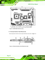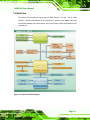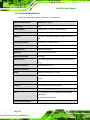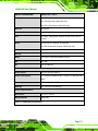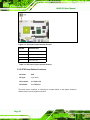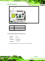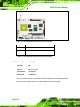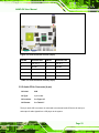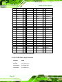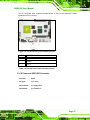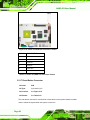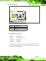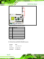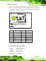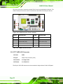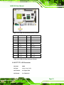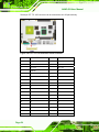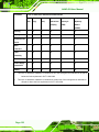
1
NANO-GX User Manual
IEI Technology Corp.
MODEL:
NANO-GX/GXTC
EPIC SBC with AMD® Geode™ GX466 333 MHz CPU,
CRT/LVDS, LAN, SATA, USB 2.0, RS-232/422/485, Audio, SATA,
CF Card Type 2, RoHS Compliant
User Manual
Page i
Rev. 1.00 – 23 June, 2009
NANO-GX User Manual
Revision
Date
Version
Changes
23 June, 2009
1.10
Modified SATA IC and BIOS
December 2006
1.00
Initial release
Page ii
NANO-GX User Manual
Copyright
COPYRIGHT NOTICE
The information in this document is subject to change without prior notice in order to
improve reliability, design and function and does not represent a commitment on the part
of the manufacturer.
In no event will the manufacturer be liable for direct, indirect, special, incidental, or
consequential damages arising out of the use or inability to use the product or
documentation, even if advised of the possibility of such damages.
This document contains proprietary information protected by copyright. All rights are
reserved. No part of this manual may be reproduced by any mechanical, electronic, or
other means in any form without prior written permission of the manufacturer.
TRADEMARKS
All registered trademarks and product names mentioned herein are used for identification
purposes only and may be trademarks and/or registered trademarks of their respective
owners.
Page iii
NANO-GX User Manual
Table of Contents
1 INTRODUCTION........................................................................................................ 13
1.1 NANO-GX CPU BOARD OVERVIEW ....................................................................... 14
1.1.1 NANO-GX Models ........................................................................................... 14
1.1.2 NANO-GX CPU Board Applications ............................................................... 14
1.1.3 NANO-GX CPU Board Benefits ...................................................................... 14
1.1.4 NANO-GX CPU Board Features ..................................................................... 15
1.2 NANO-GX OVERVIEW ............................................................................................ 15
1.2.1 NANO-GX CPU Board Connectors ................................................................. 16
1.3 DIMENSIONS ............................................................................................................. 17
1.3.1 External Interface Panel Dimensions .............................................................. 18
1.4 DATA FLOW .............................................................................................................. 19
1.4.1 Technical Specifications: ................................................................................. 20
2 UNPACKING ............................................................................................................... 22
2.1 ANTI-STATIC PRECAUTIONS ...................................................................................... 23
2.2 UNPACKING PRECAUTIONS ....................................................................................... 23
2.3 PACKING LIST........................................................................................................... 24
2.3.1 Package Contents............................................................................................. 24
3 CONNECTORS ........................................................................................................... 26
3.1 PERIPHERAL INTERFACE CONNECTORS..................................................................... 27
3.1.1 Peripheral Interface Connectors ..................................................................... 28
External Interface Panel Connectors........................................................................ 29
3.2 INTERNAL PERIPHERAL CONNECTORS ...................................................................... 29
3.2.1 12V Power Input Connector ............................................................................ 29
3.2.2 ATX Power Button Connector.......................................................................... 30
3.2.3 ATX Suspend Power Input Connector.............................................................. 31
3.2.4 Audio Connector (10-pin) ................................................................................ 32
3.2.5 Audio CD-In Connector (4-pin)....................................................................... 33
3.2.6 Backlight Inverter Connector .......................................................................... 34
3.2.7 CompactFlash® Socket..................................................................................... 35
Page iv
NANO-GX User Manual
3.2.8 Digital Input/Output (DIO) Connector............................................................ 37
3.2.9 Fan Connector (+5V) ................................................................................... 38
3.2.10 IDE Connector (44-pin)................................................................................. 39
3.2.11 Infrared Interface Connector (5-pin) ............................................................. 40
3.2.12 Keyboard/Mouse Connector .......................................................................... 41
3.2.13 Parallel Port Connector ................................................................................ 42
3.2.14 PC/104-Plus Slot............................................................................................ 43
3.2.15 PC/104 Power Input Connector..................................................................... 46
3.2.16 Power and HDD LED Connector .................................................................. 47
3.2.17 Reset Button Connector ................................................................................. 48
3.2.18 SATA Drive Connectors ................................................................................. 49
3.2.19 Serial Port and RS-422 / RS-485 Connector ................................................. 50
3.2.20 Serial Port Connectors (COM2).................................................................... 51
3.2.21 TFT LVDS LCD Connector............................................................................ 52
3.2.22 TFT TTL LCD Connector............................................................................... 53
3.3 EXTERNAL INTERFACE CONNECTORS ....................................................................... 55
3.3.1 Ethernet Connector.......................................................................................... 55
3.3.2 PS/2 Keyboard/Mouse Connector .................................................................. 56
3.3.3 RS-232 Serial Communications Connector ..................................................... 57
3.3.4 USB Combo Ports ............................................................................................ 58
3.3.5 VGA Connector ................................................................................................ 58
4 INSTALLATION ......................................................................................................... 60
4.1 ANTI-STATIC PRECAUTIONS ...................................................................................... 61
4.2 INSTALLATION CONSIDERATIONS .............................................................................. 61
4.2.1 Installation Notices .......................................................................................... 62
4.2.2 Installation Checklist ....................................................................................... 62
4.2.3 Installation Checklist ....................................................................................... 63
4.2.4 SODIMM Installation ...................................................................................... 64
4.2.5 CF Card Installation........................................................................................ 65
4.3 JUMPER SETTINGS .................................................................................................... 66
4.3.1 AT/ATX Power Mode Select ............................................................................. 67
4.3.2 COM1/2 Port RI and Voltage Select (Optional) .............................................. 68
4.3.3 CRT/LCD Mode Select..................................................................................... 69
4.3.4 LCD Panel (LVDS/TTL) Voltage Select ........................................................... 70
Page v
NANO-GX User Manual
4.3.5 LCD Panel Shift Clock Jumper........................................................................ 71
4.3.6 PC/104-Plus VIO Voltage Select Jumper & SERIRQ Select............................ 72
4.3.7 RS-422/485 Serial Port Select Jumper ............................................................ 73
4.4 CHASSIS INSTALLATION ............................................................................................ 74
4.4.1 NANO-GX Installation..................................................................................... 74
4.5 INTERNAL PERIPHERAL DEVICE CONNECTIONS ........................................................ 74
4.5.1 ATA Flat Cable Connection ............................................................................. 75
4.5.2 Keyboard/Mouse Y-cable Connector ............................................................... 76
4.5.3 Dual RS-232 Cable Connection....................................................................... 78
4.5.4 SATA Drive Connection ................................................................................... 79
4.5.5 Audio Kit Installation....................................................................................... 80
4.6 EXTERNAL PERIPHERAL INTERFACE CONNECTION ................................................... 81
4.7 SOFTWARE INSTALLATION ........................................................................................ 82
5 AWARD BIOS............................................................................................................... 84
5.1 INTRODUCTION......................................................................................................... 85
5.1.1 Starting Setup................................................................................................... 85
5.1.2 Using Setup ...................................................................................................... 85
5.1.3 Getting Help..................................................................................................... 86
5.1.4 Unable to Reboot After Configuration Changes.............................................. 86
5.1.5 Main BIOS Menu ............................................................................................. 86
5.2 STANDARD CMOS FEATURES .................................................................................. 89
5.2.1 IDE Primary Master/Slave .............................................................................. 90
5.3 ADVANCED BIOS FEATURES .................................................................................... 94
5.4 ADVANCED CHIPSET FEATURES ................................................................................ 97
5.4.1 Flat Panel Configuration................................................................................. 99
5.5 INTEGRATED PERIPHERALS..................................................................................... 101
5.5.1 IT8888 ISA Decode IO................................................................................... 108
5.5.2 IT8888 ISA Decode Memory........................................................................... 111
5.5.3 IT8888 DDMA ................................................................................................113
5.6 POWER MANAGEMENT SETUP .................................................................................114
5.7 PNP/PCI CONFIGURATIONS .....................................................................................116
5.8 PC HEALTH STATUS ................................................................................................118
A BIOS OPTIONS ........................................................................................................ 120
Page vi
NANO-GX User Manual
B TERMINOLOGY...................................................................................................... 124
C DIGITAL I/O INTERFACE..................................................................................... 128
C.1 INTRODUCTION ...................................................................................................... 129
C.2 DIO CONNECTOR PINOUTS .................................................................................... 129
C.3 ASSEMBLY LANGUAGE SAMPLES ........................................................................... 130
C.3.1 Enable the DIO Input Function..................................................................... 130
C.3.2 Enable the DIO Output Function .................................................................. 130
D WATCHDOG TIMER .............................................................................................. 131
E HAZARDOUS MATERIALS DISCLOSURE ....................................................... 134
E.1 HAZARDOUS MATERIALS DISCLOSURE TABLE FOR IPB PRODUCTS CERTIFIED AS
ROHS COMPLIANT UNDER 2002/95/EC WITHOUT MERCURY ..................................... 135
Page vii
NANO-GX User Manual
List of Figures
Figure 1-1: NANO-GX CPU Board Overview (Front Side).........................................................15
Figure 1-2: NANO-GX CPU Board Overview (Solder Side).......................................................16
Figure 1-3: NANO-GX Dimensions (mm) ....................................................................................18
Figure 1-4: External Interface Panel Dimensions (mm) ............................................................18
Figure 1-5: Data Flow Block Diagram .........................................................................................19
Figure 3-1: Connector and Jumper Locations...........................................................................27
Figure 3-2: Connector and Jumper Locations (Solder Side) ...................................................27
Figure 3-3: 12V Power Input Connector Pinouts.......................................................................30
Figure 3-4: ATX Power Button Connector Location .................................................................31
Figure 3-5: ATX Suspend Power Input Connector Location ....................................................32
Figure 3-6: Audio Connector Pinouts (10-pin)...........................................................................33
Figure 3-7: Audio CD-In Connector Pinouts (4-pin) ..................................................................34
Figure 3-8: Backlight Inverter Connector Pinout Location ......................................................35
Figure 3-9: CF Card Socket Location .........................................................................................36
Figure 3-10: DIO Connector Locations.......................................................................................37
Figure 3-11: +5V Fan Connector Location .................................................................................38
Figure 3-12: IDE Device Connector Location ............................................................................39
Figure 3-13: Infrared Connector Pinout Locations ...................................................................41
Figure 3-14: Keyboard/Mouse Connector Location ..................................................................42
Figure 3-15: Parallel Port Connector Location ..........................................................................43
Figure 3-16: PCI/104-Plus Slot Location ....................................................................................44
Figure 3-17: PC/104 Power Input Connector Pinouts ...............................................................47
Figure 3-18: Power and HDD LED Connector Location............................................................48
Figure 3-19: Reset Button Connector Locations.......................................................................49
Figure 3-20: SATA Drive Connector Locations .........................................................................50
Figure 3-21: Serial and RS-422/485 Port Connector Location .................................................51
Figure 3-22: COM2 Connector Pinout Locations ......................................................................52
Figure 3-23: LVDS LCD Connector Pinout Location.................................................................53
Figure 3-24: TFT TTL LCD Connector Pinout Locations ..........................................................54
Figure 3-25: NANO-GX Onboard External Interface Connectors.............................................55
Page viii
NANO-GX User Manual
Figure 3-26: Ethernet Connector.................................................................................................56
Figure 3-27: Mini-DIN 6 PS/2 Connector.....................................................................................57
Figure 3-28: COM1 Pinout Locations..........................................................................................58
Figure 3-29: VGA1 Connector .....................................................................................................59
Figure 4-1: SODIMM Installation .................................................................................................64
Figure 4-2: CF Card Installation ..................................................................................................66
Figure 4-3: AT Power Mode Select Jumper Pinout Location ...................................................68
Figure 4-4: COM 1/2 RI and Voltage Select Jumper Pinout Location......................................69
Figure 4-5: CRT/LCD Mode Select Jumper Pinout Location....................................................70
Figure 4-6: LCD Panel (LVDS/TTL) Voltage Select Jumper Pinout Location .........................71
Figure 4-7: LCD Panel Shift Clock Jumper Pinout Location ....................................................72
Figure 4-8: PC/104-Plus VIO Voltage & SERIRQ Select Jumper Pinout Location .................73
Figure 4-9: RS-422/485 Serial Port Select Jumper Pinout Location........................................74
Figure 4-10: IDE Cable Connection.............................................................................................76
Figure 4-11: Keyboard/mouse Y-cable Connection ..................................................................77
Figure 4-12: Dual RS-232 Cable Installation ..............................................................................78
Figure 4-13: SATA Drive Cable Connection...............................................................................79
Figure 4-14: SATA Power Drive Connection..............................................................................80
Figure 4-15: Audio Kit Connection .............................................................................................81
Figure 4-16: Introduction Screen ................................................................................................82
Figure 4-17: Available Drivers .....................................................................................................83
Page ix
NANO-GX User Manual
List of Tables
Table 1-1: NANO-GX Model Specifications................................................................................14
Table 1-2: NANO-GX Specifications ...........................................................................................21
Table 2-1: Package List Contents ...............................................................................................25
Table 3-1: Peripheral Interface Connectors ...............................................................................28
Table 3-2: Rear Panel Connectors ..............................................................................................29
Table 3-3: 12V Power Input Connector Pinouts ........................................................................30
Table 3-4: AT Power Connector Pinouts....................................................................................31
Table 3-5: ATX Suspend Power Input Connector Pinouts .......................................................32
Table 3-6: Audio Connector Pinouts (10-pin) ............................................................................33
Table 3-7: Audio CD In Connector Pinouts................................................................................34
Table 3-8: Backlight Inverter Connector Pinouts ......................................................................35
Table 3-9: CF Card Socket Pinouts.............................................................................................37
Table 3-10: DIO Connector Pinouts ............................................................................................38
Table 3-11: +5V Fan Connector Pinouts.....................................................................................39
Table 3-12: IDE Connector Pinouts.............................................................................................40
Table 3-13: Infrared Connector Pinouts .....................................................................................41
Table 3-14: Keyboard/Mouse Connector Pinouts .....................................................................42
Table 3-15: Parallel Port Connector Pinouts .............................................................................43
Table 3-16: PC/104 Slot Connector Pinouts...............................................................................45
Table 3-17: PCI-104 Slot Connector Pinouts .............................................................................46
Table 3-18: PC/104 Power Input Connector Pinouts.................................................................47
Table 3-19: Power and HDD LED Connector Pinouts ...............................................................48
Table 3-20: Reset Button Connector Pinouts ............................................................................49
Table 3-21: SATA Drive Connector Pinouts...............................................................................50
Table 3-22: Serial and RS-422/RS-485 Port Connector Pinouts ..............................................51
Table 3-23: COM2 Connector Pinouts ........................................................................................52
Table 3-24: LVDS LCD Port Connector Pinouts ........................................................................53
Table 3-25: TFT LCD Port Connector Pinouts ...........................................................................55
Table 3-26: Ethernet Connector Pinouts ....................................................................................56
Table 3-27: J7 Connector LEDs...................................................................................................56
Page x
NANO-GX User Manual
Table 3-28: Mini-DIN 6 PS/2 Connector ......................................................................................57
Table 3-29: RS-232 Serial Communications Pinouts ................................................................57
Table 3-30: J6 Connector Pinouts...............................................................................................58
Table 3-31: VGA1 Connector Pinouts.........................................................................................59
Table 4-1: Jumpers .......................................................................................................................67
Table 4-2: AT Power Mode Select Jumper Settings..................................................................67
Table 4-3: COM 1/2 RI and Voltage Select Jumper Settings ....................................................68
Table 4-4: CRT/LCD Mode Select Jumper Settings...................................................................69
Table 4-5: LVDS Voltage Selection Jumper Settings................................................................70
Table 4-6: LCD Panel Shift Clock Jumper Settings...................................................................71
Table 4-7: PC/104-Plus VIO Voltage & SERIRQ Select Jumper Settings ................................72
Table 4-8: RS-422/485 Serial Port Select Jumper Settings ......................................................73
Table 4-9: IEI Provided Cables ....................................................................................................75
Table 5-1: BIOS Navigation Keys ................................................................................................86
Page xi
NANO-GX User Manual
BIOS Menus
BIOS Menu 1: Award BIOS CMOS Setup Utility ........................................................................87
BIOS Menu 2: Standard CMOS Features....................................................................................89
BIOS Menu 3: IDE Channel Master .............................................................................................91
BIOS Menu 4: Advanced BIOS Features ....................................................................................94
BIOS Menu 5: Advanced Chipset Features................................................................................97
BIOS Menu 6: Flat Panel Configuration......................................................................................99
BIOS Menu 7: Integrated Peripherals ...................................................................................... 101
BIOS Menu 8: IT8888 ISA Decode IO ....................................................................................... 109
BIOS Menu 9: IT8888 ISA Decode Memory ............................................................................. 111
BIOS Menu 10: IT8888 DDMA ................................................................................................... 114
BIOS Menu 11: Power Management Setup ............................................................................. 115
BIOS Menu 12: PnP/PCI Configurations.................................................................................. 116
BIOS Menu 13: IRQ Resources ................................................................................................ 117
BIOS Menu 14: PC Health Status ............................................................................................. 118
Page xii
NANO-GX User Manual
Chapter
1
1 Introduction
Page 13
NANO-GX User Manual
1.1 NANO-GX CPU Board Overview
The EPIC form factor NANO-GX AMD Geode™ GX 466 is a highly integrated embedded
computer specifically optimized for multi-media applications requiring minimum installation
space. The NANO-GX is particularly suitable for low power and fan-less applications. The
NANO-GX supports a full range of functionality for an AT/ATX-compatible industrial
computer in a space-saving 3.5” profile. The NANO-GX is equipped with an onboard
low-power consumption and high performance AMD Geode™ GX 466 processor. It also
contains a DDR SODIMM socket that supports up to 512MB memory in size.
1.1.1 NANO-GX Models
The NANO-GX series has two models:
NANO-GX-466-R11
NANO-GXTC-466-R11
The specifications for the two models are show in Table 1-1.
NANO-GX-466-R11
NANO-GXTC-466-R11
Audio
YES
YES
Dual LAN
YES
YES
CRT
YES
YES
TTL LCD
YES
NO
LVDS
YES
NO
SATA
YES
NO
USB 2.0
YES
YES
Table 1-1: NANO-GX Model Specifications
1.1.2 NANO-GX CPU Board Applications
The NANO-GX motherboard has been designed for use in industrial applications where
board expansion is critical and operational reliability is essential.
1.1.3 NANO-GX CPU Board Benefits
Some of the NANO-GX motherboard benefits include,
Page 14
NANO-GX User Manual
operating reliably in harsh industrial environments with ambient temperatures
as high as 60°C
rebooting automatically if the BIOS watchdog timer detects that the system is
no longer operating
1.1.4 NANO-GX CPU Board Features
Some of the NANO-GX motherboard features are listed below:
EPIC form factor
Complies with RoHS
Embedded AMD Geode™ GX 466 CPU
Supports a maximum front side bus (FSB) speed up to 333MHz
PC/104-Plus expansion slot
Supports up to 512MB of 266MHz SODIMM DDR memory
Comes with one high performance Ethernet (10/100M) controller
Two SATA channels with transfer rates up to 150MB/s onboard
Supports four USB 2.0 devices
Integrated audio
1.2 NANO-GX Overview
Figure 1-1: NANO-GX CPU Board Overview (Front Side)
Page 15
NANO-GX User Manual
Figure 1-2: NANO-GX CPU Board Overview (Solder Side)
1.2.1 NANO-GX CPU Board Connectors
The NANO-GX has the following connectors onboard:
1 x ATX power button connector
1x ATX Suspend power input connector
1x Audio CD-IN connector
1x Audio connector
1x Backlight inverter connector
1x Digital I/O Connector
1x Fan connector
1x IrDA Infrared interface connector
1x Keyboard / mouse connector
1x Parallel port connector
1x Power and HDD LED connector
1x Power input connector
1x PC/104-Plus slot
Page 16
NANO-GX User Manual
1x PC/104-Plus power input connector
1x Reset button
2 x Serial ATA connectors
4 x Serial port RS2-232 connectors
1 x Serial and RS-422/485 port connector
1x TFT LVDS LCD Panel Connector
1x TFT TTL LCD (Hirose DF13-40DP-1.25V) connector
The NANO-GX has the following external peripheral interface connectors:
1 x Ethernet connector
1 x PS/2 Keyboard/mouse connector
1 x RS-232 connector
4 x USB 2.0 port connectors
1 x VGA connector
The NANO-GX has the following onboard jumpers:
AT/ATX power mode select
COM1/2 port RI and voltage selection (optional)
CRT/LCD mode select
LCD panel (LVDS/TTL) voltage select
LCD panel shift clock setting
PC/104-Plus VIO voltage select jumper & SERIRQ select
RS-422/RS-485 select
The location of these connectors on the motherboard can be seen in Figure 3-1. These
connectors are fully described in Chapter 3.2.
1.3 Dimensions
The dimensions of the board are listed below:
Length:
165mm
Width:
115mm
Page 17
NANO-GX User Manual
Figure 1-3: NANO-GX Dimensions (mm)
1.3.1 External Interface Panel Dimensions
External peripheral interface connector panel dimensions are shown in Figure 1-4.
Figure 1-4: External Interface Panel Dimensions (mm)
Page 18
NANO-GX User Manual
1.4 Data Flow
The NANO-GX motherboard comes with an AMD Geode™ GX 466
and an AMD
Geode™ CS5536 linked together by the GeodeLink™ Interface Unit. Figure 1-5 shows
the data flow between the system chipset, the CPU and other components installed on the
motherboard.
Figure 1-5: Data Flow Block Diagram
Page 19
NANO-GX User Manual
1.4.1 Technical Specifications:
NANO-GX motherboard technical specifications are listed below.
Specification/Model
NANO-GX / GXTC
Form Factor
EPIC
CPU Supported
AMD® Geode™ GX466 333MHz processor
Integrated Graphics
AMD® Geode™ GX466
Memory
One 200-pin 266/200MHz DDR SO-DIMM slot (up to 512
MB)
Southbridge Chipset
AMD Geode™ CS5536 Chipset
BIOS
Award BIOS
Compatible OS
Microsoft Windows XP
Digital I/O
8-bit, 4-bit input/4-bit output
Ethernet Controllers
RTL8100C
RAID Controller
VIA VT6421A with RAID 0,1 function support (NANO-GX
only)
Super I/O Controller
Winbond W83627EHG
Serial Port Controller
Fintek F81216
Audio
Realtek ALC203 with AC’97 codec
Real Time Clock
256 bytes of battery-backed RAM, 32.768 KHz crystal, 3 V
battery
Watchdog Timer
Software programmable supports 1~255 sec. system reset
Infrared
One Infrared interface by pin header
Expansion
PCI
One PC/104-Plus via ITE IT8888G PCI-to-ISA bridge
(NANO-GX)
One PC-104 (NANO-GXTC)
I/O Interface Connectors
Page 20
NANO-GX User Manual
Specification/Model
NANO-GX / GXTC
Display
One VGA
One LVDS (internal, NANO-GX only)
One TTL LCD (internal, NANO-GX only)
Ethernet
One RJ-45
Keyboard/Mouse
One PS/2 KB/MS
LPT
One IEEE 1284 parallel (supports normal, EPP and ECP
modes)
Serial
Six RS-232 (one external, five internal)
One RS-232/422/485 (internal, NANO-GX only)
USB 2.0/1.1
Four USB 2.0 ports
Storage
SATA
Two SATA1 connectors (NANO-GX only)
IDE
One IDE
CF
One CF card slot
Environmental and Power Specifications
Power Supply
12V only, AT/ATX support
Power Consumption
12 V @ 0.83A (AMD® Geode™ GX466, 512 MB DDR 400
MHz)
Operating temperature
0ºC ~ 60ºC (32ºF~140ºF)
Humidity
0% ~ 95% (non-condensing)
Physical Specifications
Dimensions
115 mm x 165 mm
Weight GW/NW
950g/350g
Table 1-2: NANO-GX Specifications
Page 21
NANO-GX User Manual
Chapter
2
2 Unpacking
Page 22
NANO-GX User Manual
2.1 Anti-static Precautions
WARNING!
Static electricity can destroy certain electronics. Make sure to follow the
ESD precautions to prevent damage to the product, and injury to the
user.
Make sure to adhere to the following guidelines:
Wear an anti-static wristband: Wearing an anti-static wristband can prevent
electrostatic discharge.
Self-grounding: Touch a grounded conductor every few minutes to discharge
any excess static buildup.
Use an anti-static pad: When configuring any circuit board, place it on an
anti-static mat.
Only handle the edges of the PCB: Don't touch the surface of the
motherboard. Hold the motherboard by the edges when handling.
2.2 Unpacking Precautions
When the NANO-GX is unpacked, please do the following:
Follow the antistatic guidelines above.
Make sure the packing box is facing upwards when opening.
Make sure all the packing list items are present.
Page 23
NANO-GX User Manual
2.3 Packing List
NOTE:
If any of the components listed in the checklist below are missing, do
not proceed with the installation. Contact the IEI reseller or vendor the
NANO-GX was purchased from or contact an IEI sales representative
directly by sending an email to [email protected].
32
2.3.1 Package Contents
The NANO-GX is shipped with the following components:
Quantity
Item
1
NANO-GX / GXTC
1
12V Power Cable
1
Audio Cable
1
ATA33 Flat Cable
Page 24
Image
NANO-GX User Manual
1
Dual RS-232 Cable
1
Mini jumper pack
1
KB/MS Y cable
2
SATA cable
1
SATA power cable
1
Quick Installation Guide
1
Utility CD
Table 2-1: Package List Contents
Page 25
NANO-GX User Manual
Chapter
3
3 Connectors
Page 26
NANO-GX User Manual
3.1 Peripheral Interface Connectors
Figure 3-1 and Figure 3-2 show all the onboard peripheral connectors, rear panel
peripheral connectors and onboard jumpers. Section 3.1.1 lists all the peripheral interface
connectors.
Figure 3-1: Connector and Jumper Locations
Figure 3-2: Connector and Jumper Locations (Solder Side)
Page 27
NANO-GX User Manual
3.1.1 Peripheral Interface Connectors
Table 3-1 shows a list of the peripheral interface connectors on the NANO-GX. Detailed
descriptions of these connectors can be found below.
Connector
Type
Label
12V Power input connector
4-pin wafer
CN2
ATX power button connector
2-pin wafer
CN5
ATX Suspend power input connector
3-pin wafer
CN3
Audio CD-IN connector
4-pin header
CN8
Audio connector
10-pin box header
CN9
Backlight inverter connector
5-pin wafer
CN26
Digital I/O connector
10-pin header
CN18
CF card slot
50-pin header (2x25)
CN35
Fan connector
3-pin wafer
CN4
IrDA Infrared interface connector
5-pin wafer
CN32
Keyboard / mouse connector
6-pin wafer
CN30
Parallel port connector
26-pin header
CN20
Power and HDD LED connector
6-pin wafer
CN12
PC/104-Plus slot
140-pin PC/104+ 120-pin PCI-104
CN7
PC/104-Plus power input connector
3-pin wafer
CN25
Reset button
2-pin wafer
CN6
Serial ATA connectors
7-pin SATA connector
CN10, CN11
Serial port RS2-232 connectors
10-pin header
CN14 - 17
Serial and RS-422/485 port connector
14-pin header
CN19
TFT LVDS LCD panel connector
20-pin crimp
CN23
TFT TTL LCD (Hirose
40-pin crimp
CN22
DF13-40DP-1.25V) connector
Table 3-1: Peripheral Interface Connectors
Page 28
NANO-GX User Manual
External Interface Panel Connectors
Table 3-2 lists the rear panel connectors on the NANO-GX. Detailed descriptions of these
connectors can be found in Section 3.1.
Connector
Type
Label
Ethernet connector
RJ-45
CN27
PS/2 Keyboard/mouse
Mini-DIN 6 PS/2
CN31
RS-232 serial port connector
9-pin male
CN21
USB 2.0 ports
Combo USB port
CN28, CN29
VGA port connector
15-pin female
CN24
connector
Table 3-2: Rear Panel Connectors
3.2 Internal Peripheral Connectors
Internal peripheral connectors are found on the motherboard and are only accessible
when the motherboard is outside of the chassis. This section has complete descriptions of
all the internal, peripheral connectors on the NANO-GX.
3.2.1 12V Power Input Connector
CN Label:
CN2
CN Type:
4-pin wafer (2x2)
CN Location:
See Figure 3-3
CN Pinouts:
See Table 3-3
Page 29
NANO-GX User Manual
Figure 3-3: 12V Power Input Connector Pinouts
PIN NO.
DESCRIPTION
1
GROUND
2
GROUND
3
Power IN(+12V)
4
Power IN(+12V)
Table 3-3: 12V Power Input Connector Pinouts
3.2.2 ATX Power Button Connector
CN Label:
CN5
CN Type:
2-pin wafer
CN Location:
See Figure 3-4
CN Pinouts:
See Table 3-4
The power button connector is connected to a power switch on the system chassis to
enable users to turn the system on and off.
Page 30
NANO-GX User Manual
Figure 3-4: ATX Power Button Connector Location
PIN NO.
DESCRIPTION
1
ATX Power button +
2
ATX Power button -
Table 3-4: AT Power Connector Pinouts
3.2.3 ATX Suspend Power Input Connector
CN Label:
CN3
CN Type:
3-pin wafer
CN Location:
See Figure 3-5
CN Pinouts:
See Table 3-5
The suspend power input connector connects to an ATX power supply.
Page 31
NANO-GX User Manual
Figure 3-5: ATX Suspend Power Input Connector Location
PIN NO.
DESCRIPTION
1
5VSB
2
NC
3
PS_ON
Table 3-5: ATX Suspend Power Input Connector Pinouts
3.2.4 Audio Connector (10-pin)
CN Label:
CN9
CN Type:
10-pin box header
CN Location:
See Figure 3-6
CN Pinouts:
See Table 3-6
The 10-pin audio connector is connected to external audio devices including speakers and
microphones for the input and output of audio signals to and from the system.
Page 32
NANO-GX User Manual
Figure 3-6: Audio Connector Pinouts (10-pin)
PIN NO.
DESCRIPTION
PIN NO.
DESCRIPTION
1
LINE_OUT_R
2
LINE_IN_R
3
GROUND
4
GROUND
5
LINE_OUT_L
6
LINE_IN_L
7
GROUND
8
GROUND
9
MIC1
10
NC
Table 3-6: Audio Connector Pinouts (10-pin)
3.2.5 Audio CD-In Connector (4-pin)
CN Label:
CN8
CN Type:
4-pin header
CN Location:
See Figure 3-7
CN Pinouts:
See Table 3-7
The 4-pin audio CD-in connector is connected to an external audio CD device for the input
and output of audio signals from a CD player to the system.
Page 33
NANO-GX User Manual
Figure 3-7: Audio CD-In Connector Pinouts (4-pin)
PIN NO.
DESCRIPTION
1
CD Signal (Left)
2
Ground
3
Ground
4
CD Signal (Right)
Table 3-7: Audio CD In Connector Pinouts
3.2.6 Backlight Inverter Connector
CN Label:
CN26
CN Type:
5-pin wafer
CN Location:
See Figure 3-8
CN Pinouts:
See Table 3-8
The backlight inverter connector provides the backlight on the LCD display connected to
the NANO-GX with +12V of power.
Page 34
NANO-GX User Manual
Figure 3-8: Backlight Inverter Connector Pinout Location
PIN NO.
DESCRIPTION
1
BL_ADJ (DEFAULT: GND)
2
GND
3
VCC12
4
GND
5
VDD_EN
Table 3-8: Backlight Inverter Connector Pinouts
3.2.7 CompactFlash® Socket
CN Label:
CN35 (solder side)
CN Type:
50-pin header (2x25)
CN Location:
See Figure 3-9
CN Pinouts:
See Table 3-9
A CF Type I or Type II memory card is inserted to the CF socket on the solder side of the
NANO-GX.
Page 35
NANO-GX User Manual
Figure 3-9: CF Card Socket Location
PIN NO.
DESCRIPTION
PIN NO.
DESCRIPTION
1
GROUND
26
GND
2
DATA 3
27
DATA 11
3
DATA 4
28
DATA 12
4
DATA 5
29
DATA 13
5
DATA 6
30
DATA 14
6
DATA 7
31
DATA 15
7
HDC_CS0#
32
HDC_CS1
8
GND
33
N/C
9
GROUND
34
IOR#
10
GND
35
IOW#
11
GND
36
VCC5
12
GND
37
IRQ15
13
VCC5
38
VCC5
14
GND
39
CSEL
15
GND
40
N/C
16
GND
41
HDD_RESET
17
GND
42
RDY
Page 36
NANO-GX User Manual
18
SA2
43
DRQ
19
SA1
44
DACK#
20
SA0
45
HDD_ACTIVE#
21
DATA 0
46
CABLEID
22
DATA 1
47
DATA 8
23
DATA 2
48
DATA 9
24
N/C
49
DATA 10
25
GND
50
GROUND
Table 3-9: CF Card Socket Pinouts
3.2.8 Digital Input/Output (DIO) Connector
CN Label:
CN18
CN Type:
10-pin header (2x5)
CN Location:
See Figure 3-10
CN Pinouts:
See Table 3-10
The digital input/output connector is managed through a Super I/O chip. The DIO
connector pins are user programmable.
Figure 3-10: DIO Connector Locations
Page 37
NANO-GX User Manual
PIN NO. DESCRIPTION
PIN NO. DESCRIPTION
1
GND
2
VCC5
3
Output 0
4
Output 1
5
Output 2
6
Output 3
7
Input 0
8
Input 1
9
Input 2
10
Input 3
Table 3-10: DIO Connector Pinouts
3.2.9 Fan Connector
(+5V)
CN Label:
CN4
CN Type:
3-pin wafer
CN Location:
See Figure 3-11
CN Pinouts:
See Table 3-11
The cooling fan connector provides a 5V, 500mA current to a system cooling fan. The
connector has a "rotation" pin to get rotation signals from fans and notify the system so the
system BIOS can recognize the fan speed. Please note that only specified fans can issue
the rotation signals.
Figure 3-11: +5V Fan Connector Location
Page 38
NANO-GX User Manual
PIN NO.
DESCRIPTION
1
Fan Speed Detect
2
+5V
3
GND
Table 3-11: +5V Fan Connector Pinouts
3.2.10 IDE Connector (44-pin)
CN Label:
CN13
CN Type:
44-pin box header (2x22)
CN Location:
See Figure 3-12
CN Pinouts:
See Table 3-12
One 44-pin IDE device connector on the NANO-GX supports connectivity to two hard disk
drives.
Figure 3-12: IDE Device Connector Location
PIN NO.
DESCRIPTION
PIN NO.
DESCRIPTION
1
RESET#
2
GROUND
3
DATA 7
4
DATA 8
5
DATA 6
6
DATA 9
7
DATA 5
8
DATA 10
9
DATA 4
10
DATA 11
Page 39
NANO-GX User Manual
11
DATA 3
12
DATA 12
13
DATA 2
14
DATA 13
15
DATA 1
16
DATA 14
17
DATA 0
18
DATA 15
19
GROUND
20
N/C
21
IDE DRQ
22
GROUND
23
IOW#
24
GROUND
25
IOR#
26
GROUND
27
IDE CHRDY
28
GROUND
29
IDE DACK
30
GROUND–DEFAULT
31
INTERRUPT
32
N/C
33
SA1
34
N/C
35
SA0
36
SA2
37
HDC CS0#
38
HDC CS1#
39
HDD ACTIVE#
40
GROUND
41
VCC
42
VCC
43
GROUND
44
N/C
Table 3-12: IDE Connector Pinouts
3.2.11 Infrared Interface Connector (5-pin)
CN Label:
CN32
CN Type:
5-pin wafer
CN Location:
See Figure 3-13
CN Pinouts:
See Table 3-13
The infrared interface connector supports both Serial Infrared (SIR) and Amplitude Shift
Key Infrared (ASKIR) interfaces.
Page 40
NANO-GX User Manual
Figure 3-13: Infrared Connector Pinout Locations
PIN NO.
DESCRIPTION
1
VCC5
2
NC
3
IR-RX
4
GND
5
IR-TX
Table 3-13: Infrared Connector Pinouts
3.2.12 Keyboard/Mouse Connector
CN Label:
CN30
CN Type:
6-pin wafer
CN Location:
See Figure 3-14
CN Pinouts:
See Table 3-14
The keyboard and mouse connector can be connected to a standard PS/2 cable or PS/2
Y-cable to add keyboard and mouse functionality to the system.
Page 41
NANO-GX User Manual
Figure 3-14: Keyboard/Mouse Connector Location
PIN NO.
DESCRIPTION
1
VCC5
2
Mouse DATA
3
Mouse Clock
4
Keyboard DATA
5
Keyboard Clock
6
GROUND
Table 3-14: Keyboard/Mouse Connector Pinouts
3.2.13 Parallel Port Connector
CN Label:
CN20
CN Type:
26-pin header
CN Location:
See Figure 3-15
CN Pinouts:
See Table 3-15
The 26-pin parallel port connector connects to a parallel port connector interface or some
other parallel port device such as a printer.
Page 42
NANO-GX User Manual
Figure 3-15: Parallel Port Connector Location
PIN NO.
DESCRIPTION
PIN NO.
DESCRIPTION
1
PRN_STB#
2
PRN_AFD#
3
PRN_PD0
4
PRN_ERR#
5
PRN_PD1
6
PRN_INIT#
7
PRN_PD2
8
PRN_SLIN#
9
PRN_PD3
10
GND
11
PRN_PD4
12
GND
13
PRN_PD5
14
GND
15
PRN_PD6
16
GND
17
PRN_PD7
18
GND
19
PRN_ACK#
20
GND
21
PRN_BUSY
22
GND
23
PRN_PE
24
GND
25
PRN_SLCT
26
NC
Table 3-15: Parallel Port Connector Pinouts
3.2.14 PC/104-Plus Slot
The NANO-GX features a PC/104-Plus slot for expansion. PC/104-Plus consists of a
PC/104 slot and a PCI-104 slot.
Page 43
NANO-GX User Manual
The PC/104 slot enables a PC/104 compatible expansion module to be connected to the
board. The PCI-104 slot enables a PCI-104 compatible expansion module to be
connected to the board.
CN Label:
CN7
CN Type:
104-pin PC/104 slot, 120-pin PCI-104 slot
CN Location:
See Figure 3-16
CN Pinouts:
See Table 3-16 for PC/104 slot pinouts
See Table 3-17 for PCI-104 slot pinouts
Figure 3-16: PCI/104-Plus Slot Location
Pin No.
Column A
Column B
Column C
Column D
1
IOCHK-
GROUND
GROUND
GROUND
2
SD7
RSTDRV
SBHE-
MCS16-
3
SD6
+5V
SA23
IOCS16-
4
SD5
IRQ9
SA22
IRQ10
5
SD4
-5V
SA21
IRQ11
6
SD3
DREQ2
SA20
IRQ12
7
SD2
-12V
SA19
IRQ15
8
SD1
ZWS-
SA18
IRQ14
9
SD0
+12V
SA17
DACK0-
Page 44
NANO-GX User Manual
10
IOCHRDY
GROUND
MEMR-
DREQ0
11
AEN
SMEMW-
MEMW-
DACK5-
12
SA19
SMEMR-
SD8
DRREQ5
13
SA18
IOW-
SD9
DACK6-
14
SA17
IOR-
SD10
DREQ6
15
SA16
DACK3-
SD11
DACK7-
16
SA15
DREQ3
SD12
DREQ7
17
SA14
DACK1-
SD13
+5V
18
SA13
DREQ1
SD14
MASTER-
19
SA12
REFRESH-
SD15
GROUND
20
SA11
ISACLK
NC
GROUND
21
SA10
IRQ7
22
SA9
IRQ6
23
SA8
IRQ5
24
SA7
IRQ4
25
SA6
IRQ3
26
SA5
DACK2-
27
SA4
TC
28
SA3
BALE
29
SA2
+5V
30
SA1
ISA_OSC
31
SA0
GROUND
32
GROUND
GROUND
Table 3-16: PC/104 Slot Connector Pinouts
Pin
Description
Pin
Description
Pin
Description
Pin
Description
A1
GND
B1
SERIRQ#
C1
VCC5
D1
AD0
A2
VI0
B2
AD2
C2
AD1
D2
VCC5
A3
AD5
B3
GND
C3
AD4
D3
AD3
A4
BE0#
B4
AD7
C4
GND
D4
AD6
A5
GND
B5
AD9
C5
AD8
D5
GND
A6
AD11
B6
VIO
C6
AD10
D6
GND
A7
AD14
B7
AD13
C7
GND
D7
AD12
Page 45
NANO-GX User Manual
A8
VCC3
B8
BE1#
C8
AD15
D8
VCC3
A9
PULL 3V
B9
GND
C9
PULL 3V
D9
PAR
A10
GND
B10
PULL 3V
C10
VCC3
D10
PULL 3V
A11
STOP#
B11
VCC3
C11
PULL 3V
D11
GND
A12
VCC3
B12
TRDY#
C12
GND
D12
DEVSEL#
A13
FRAME#
B13
GND
C13
IRDY#
D13
VCC3
A14
GND
B14
AD16
C14
VCC3
D14
BE2#
A15
AD18
B15
VCC3
C15
AD17
D15
GND
A16
AD21
B16
AD20
C16
GND
D16
AD19
A17
VCC3
B17
AD23
C17
AD22
D17
VCC3
A18
IDSEL0
B18
GND
C18
IDSEL1
D18
IDSEL2
A19
AD24
B19
BE3#
C19
VIO
D19
IDSEL3
A20
GND
B20
AD26
C20
AD25
D20
GND
A21
AD29
B21
VCC5
C21
AD28
D21
AD27
A22
VCC5
B22
AD30
C22
GND
D22
AD31
A23
REQ0
B23
GND
C23
REQ1
D23
VIO
A24
GND
B24
REQ2
C24
VCC5
D24
GNT0
A25
GNT1
B25
VIO
C25
GNT2
D25
GND
A26
VCC5
B26
CLOCK0
C26
GND
D26
CLOCK1
A27
CLOCK2
B27
VCC5
C27
CLOCK3
D27
GND
A28
GND
B28
INTD#
C28
VCC5
D28
RESET
A29
+12V
B29
INTA#
C29
INTB#
D29
INTC#
A30
-12V
B30
NC
C30
NC
D30
GND
Table 3-17: PCI-104 Slot Connector Pinouts
3.2.15 PC/104 Power Input Connector
CN Label:
CN25
CN Type:
3-pin wafer (1x3)
CN Location:
See Figure 3-17
CN Pinouts:
See Table 3-18
Page 46
NANO-GX User Manual
The PC/104 power input connector provides power to the PC/104 expansion module
installed on the PC/104 slot.
Figure 3-17: PC/104 Power Input Connector Pinouts
PIN NO. DESCRIPTION
1
-VCC5
2
GROUND
3
-VCC12
Table 3-18: PC/104 Power Input Connector Pinouts
3.2.16 Power and HDD LED Connector
CN Label:
CN12
CN Type:
6-pin wafer
CN Location:
See Figure 3-15
CN Pinouts:
See Table 3-15
Page 47
NANO-GX User Manual
Figure 3-18: Power and HDD LED Connector Location
PIN NO.
DESCRIPTION
1
VCC5
2
GROUND
3
PWRLED+
4
PWRLED-
5
HDD LED+
6
HDD LED-
Table 3-19: Power and HDD LED Connector Pinouts
3.2.17 Reset Button Connector
CN Label:
CN6
CN Type:
2-pin wafer (1x2)
CN Location:
See Figure 3-19
CN Pinouts:
See Table 3-20
The reset button connector is connected to a reset switch on the system chassis to enable
users to reboot the system when the system is turned on.
Page 48
NANO-GX User Manual
Figure 3-19: Reset Button Connector Locations
PIN NO.
DESCRIPTION
1
Reset button +
2
Reset button -
Table 3-20: Reset Button Connector Pinouts
3.2.18 SATA Drive Connectors
CN Label:
CN10 and CN11
CN Type:
7-pin SATA drive connectors
CN Location:
See Figure 3-20
CN Pinouts:
See Table 3-21
The two SATA drive connectors are each connected to a first generation SATA drive. First
generation SATA drives transfer data at speeds as high as 150Mb/s. The SATA drives can
be configured in a RAID configuration.
Page 49
NANO-GX User Manual
Figure 3-20: SATA Drive Connector Locations
PIN NO. DESCRIPTION
1
GND
2
TX+
3
TX-
4
GND
5
RX-
6
RX+
7
GND
Table 3-21: SATA Drive Connector Pinouts
3.2.19 Serial Port and RS-422 / RS-485 Connector
CN Label:
CN19
CN Type:
14-pin header (2x7)
CN Location:
See Figure 3-21
CN Pinouts:
See Table 3-22
Page 50
NANO-GX User Manual
The 14-pin serial port connector connects to the COM 2 serial communications channels.
COM2 is a multi function channel. In default mode COM 2 is an RS-232 serial
communication channel but, with the JP4 jumper, can be configured as either an RS-422
or RS-485 serial communications channel.
Figure 3-21: Serial and RS-422/485 Port Connector Location
PIN NO.
DESCRIPTION
PIN NO.
DESCRIPTION
1
DCD
2
DSR
3
RXD
4
RTS
5
TXD
6
CTS
7
DTR
8
RI
9
GROUND
10
GROUND
11
TXD485+
12
TXD485#
13
RXD485+
14
RXD485#
Table 3-22: Serial and RS-422/RS-485 Port Connector Pinouts
3.2.20 Serial Port Connectors (COM2)
CN Label:
CN14, CN15, CN16, CN17
CN Type:
10-pin header (2x5)
CN Location:
See Figure 3-22
CN Pinouts:
See Table 3-23
Page 51
NANO-GX User Manual
The 10-pin serial port connectors provide RS-232 serial communications channels. The
COM 2 serial port connectors can be connected to external RS-232 serial port devices.
Figure 3-22: COM2 Connector Pinout Locations
PIN NO.
DESCRIPTION
PIN NO.
DESCRIPTION
1
Data Carrier Direct (DCD)
2
Data Set Ready (DSR)
3
Receive Data (RXD)
4
Request To Send (RTS)
5
Transmit Data (TXD)
6
Clear To Send (CTS)
7
Data Terminal Ready (DTR)
8
Ring Indicator (RI)
9
Ground (GND)
10
Ground (GND)
Table 3-23: COM2 Connector Pinouts
3.2.21 TFT LVDS LCD Connector
CN Label:
CN23
CN Type:
20-pin crimp connector (2x10)
CN Location:
See Figure 3-23
CN Pinouts:
See Table 3-24
The 20-pin LVDS LCD connector can be connected to single channel 18-bit LVDS panel.
Page 52
NANO-GX User Manual
Figure 3-23: LVDS LCD Connector Pinout Location
PIN NO. DESCRIPTION
PIN NO. DESCRIPTION
2
GROUND
1
GROUND
4
LVD_Y0-
3
LVD_Y0+
6
LVD_Y1-
5
LVD_Y1+
8
LVD_Y2-
7
LVD_Y2
10
LVD_CLK-
9
LVD_CLK+
12
NC
11
NC
14
GROUND
13
GROUND
16
NC
15
NC
18
LVD_ VCC
17
LVD_ VCC
20
LVD_ VCC
19
LVD_ VCC
Table 3-24: LVDS LCD Port Connector Pinouts
3.2.22 TFT TTL LCD Connector
CN Label:
CN22
CN Type:
40-pin crimp (2x20)
CN Location:
See Figure 3-24
CN Pinouts:
See Table 3-25
Page 53
NANO-GX User Manual
The 40-pin TFT TTL LCD connector can be connected to an LCD panel directly.
Figure 3-24: TFT TTL LCD Connector Pinout Locations
PIN NO.
DESCRIPTION
PIN NO.
DESCRIPTION
2
LCD_VCC
1
LCD_VCC
4
GROUND
3
GROUND
6
LCD_VCC
5
LCD_VCC
8
GROUND
7
NC
10
B1
9
B0
12
B3
11
B2
14
B5
13
B4
16
B7
15
B6
18
G1
17
G0
20
G3
19
G2
22
G5
21
G4
24
G7
23
G6
26
R1
25
R0
28
R3
27
R2
30
R5
29
R4
32
R7
31
R6
34
GROUND
33
GROUND
36
FPVS
35
FPCLK
Page 54
NANO-GX User Manual
38
FPHS
37
FPDE
40
FPENVEE
39
NC
Table 3-25: TFT LCD Port Connector Pinouts
3.3 External Interface Connectors
Figure 3-25 shows the NANO-GX motherboard external interface connectors. The
NANO-GX onboard external interface connectors are listed below and shown in Figure
3-25:
1 x Ethernet connector
1 x Keyboard/Mouse connector
1 x Serial communications port
2 x USB combo ports
1 x VGA port
Figure 3-25: NANO-GX Onboard External Interface Connectors
3.3.1 Ethernet Connector
CN Label:
CN27
CN Type:
RJ-45
CN Location:
See Figure 3-25
CN Pinouts:
See Table 3-26
A 10/100 Mbps connection can be made between the Ethernet connector and a Local
Area Network (LAN) through a network hub.
Page 55
NANO-GX User Manual
PIN
DESCRIPTION
PIN
DESCRIPTION
1
TX-
5
N/C
2
N/C
6
RX-
3
TX-
7
N/C
4
RX+
8
N/C
Table 3-26: Ethernet Connector Pinouts
Figure 3-26: Ethernet Connector
The RJ-45 Ethernet connector has two status LEDs, one green and one yellow. The green
LED indicates activity on the port and the yellow LED indicates the port is linked.
SPEED LED
Status
Description
GREEN
ON: 100MB
LINK LED
Status
YELLOW
OFF: 10MB
Description
ON: Linked
Flashing: Activity
Table 3-27: J7 Connector LEDs
3.3.2 PS/2 Keyboard/Mouse Connector
CN Label:
CN31
CN Type:
Mini-DIN 6 PS/2
CN Location:
See Figure 3-25
CN Pinouts:
See Table 3-28 and Figure 3-27
The NANO-GX has a mini-DIN 6 PS/2 connector on the mounting bracket for easy
connection to a PS/2 keyboard or PS/2 mouse. The card comes with a cable to convert
the mini-DIN 6 PS/2 into two mini-DIN 6 PS/2 connectors for keyboard and mouse
connection.
Page 56
NANO-GX User Manual
Figure 3-27: Mini-DIN 6 PS/2 Connector
PIN NO. DESCRIPTION
1
KEYBOARD DATA
2
MOUSE DATA
3
GND
4
VCC
5
KEYBOARD CLOCK
6
MOUSE CLOCK
Table 3-28: Mini-DIN 6 PS/2 Connector
3.3.3 RS-232 Serial Communications Connector
CN Label:
CN21
CN Type:
RS-232 serial connector
CN Location:
See Figure 3-25
CN Pinouts:
See Table 3-29 and Figure 3-28
The RS-232 serial connector provides serial connection in the RS-232 mode.
PIN
DESCRIPTION
PIN
DESCRIPTION
1
DCD1
2
DSR1
3
RX1
4
RTS1
5
TX1
6
CTS1
7
DTR1
8
RI1
9
GND
Table 3-29: RS-232 Serial Communications Pinouts
Page 57
NANO-GX User Manual
Figure 3-28: COM1 Pinout Locations
3.3.4 USB Combo Ports
CN Label:
CN28, CN29
CN Type:
USB Combo ports
CN Location:
See Figure 3-25
CN Pinouts:
See Table 3-30
The USB combo port provides connectivity to additional USB devices through an adapter
cable. Various adapters may come with USB ports on a slot bracket or ports that can be
attached to D-SUB openings on a chassis. USB devices connect directly to the USB
connectors on the rear panel.
PIN
DESCRIPTION
PIN
DESCRIPTION
1
5V
2
GND
3
USBP2N
4
USBP3P
5
USBP2P
6
USBP3N
7
GND
8
5V
Table 3-30: J6 Connector Pinouts
3.3.5 VGA Connector
CN Label:
CN24
CN Type:
HD-D-sub 15 female connector
CN Location:
See Figure 3-25
CN Pinouts:
See Figure 3-29 and Table 3-31
Page 58
NANO-GX User Manual
The standard 15-pin female VGA connector connects to a CRT or LCD monitor.
PIN
DESCRIPTION
PIN
DESCRIPTION
PIN
DESCRIPTION
1
RED
6
GROUND
11
NC
2
GREEN
7
GROUND
12
DDCDAT
3
BLUE
8
GROUND
13
HSYNC
4
NC
9
NC
14
VSYNC
5
GROUND
10
GROUND
15
DDCCLK
Table 3-31: VGA1 Connector Pinouts
Figure 3-29: VGA1 Connector
Page 59
NANO-GX User Manual
Chapter
4
4 Installation
Page 60
NANO-GX User Manual
4.1 Anti-static Precautions
WARNING:
Failure to take ESD precautions during the installation of the
PM-LX2-800 may result in permanent damage to the PM-LX2-800 and
severe injury to the user.
Electrostatic discharge (ESD) can cause serious damage to electronic components,
including the PM-LX2-800. Dry climates are especially susceptible to ESD. It is therefore
critical that whenever the PM-LX2-800 or any other electrical component is handled, the
following anti-static precautions are strictly adhered to.
Wear an anti-static wristband: - Wearing a simple anti-static wristband can
help to prevent ESD from damaging the board.
Self-grounding:- Before handling the board touch any grounded conducting
material. During the time the board is handled, frequently touch any
conducting materials that are connected to the ground.
Use an anti-static pad: When configuring the PM-LX2-800, place it on an
antic-static pad. This reduces the possibility of ESD damaging the
PM-LX2-800.
Only handle the edges of the PCB:-: When handling the PCB, hold the PCB
by the edges.
4.2 Installation Considerations
NOTE:
The following installation notices and installation considerations should
be read and understood before the PM-LX2-800 is installed. All
installation notices should be strictly adhered to. Failing to adhere to
these precautions may lead to severe damage of the PM-LX2-800 and
injury to the person installing the motherboard.
Page 61
NANO-GX User Manual
4.2.1 Installation Notices
WARNING:
The installation instructions described in this manual should be carefully
followed in order to prevent damage to the PM-LX2-800, PM-LX2-800
components and injury to the user.
Before and during the installation please DO the following:
Read the user manual:
o
The user manual provides a complete description of the PM-LX2-800
installation instructions and configuration options.
Wear an electrostatic discharge cuff (ESD):
o
Electronic components are easily damaged by ESD. Wearing an ESD cuff
removes ESD from the body and helps prevent ESD damage.
Place the PM-LX2-800 on an antistatic pad:
o
When installing or configuring the motherboard, place it on an antistatic
pad. This helps to prevent potential ESD damage.
Turn all power to the PM-LX2-800 off:
o
When working with the PM-LX2-800, make sure that it is disconnected
from all power supplies and that no electricity is being fed into the system.
Before and during the installation of the PM-LX2-800 DO NOT:
Remove any of the stickers on the PCB board. These stickers are required for
warranty validation.
Use the product before verifying all the cables and power connectors are
properly connected.
Allow screws to come in contact with the PCB circuit, connector pins, or its
components.
4.2.2 Installation Checklist
The following checklist is provided to ensure the PM-LX2-800 is properly installed.
Page 62
NANO-GX User Manual
All the items in the packing list are present
A compatible memory module is properly inserted into the slot
The CF Type I or CF Type II card is properly installed into the CF socket
The jumpers have been properly configured
The PM-LX2-800 is inserted into a chassis with adequate ventilation
The correct power supply is being used
The following devices are properly connected
o
o
o
o
o
o
o
o
o
o
o
IDE drives
RS-232 devices
RS-422/485 devices
Keyboard and mouse
LAN
LCD backlight
LPT device
Power
TTL screen
USB port
VGA port
4.2.3 Installation Checklist
The following checklist is provided to ensure the NANO-GX is properly installed.
All the items in the packing list are present
A compatible memory module is properly inserted into the slot
The CF Type I or CF Type II card is properly installed into the CF socket
The jumpers have been properly configured
The NANO-GX is inserted into a chassis with adequate ventilation
The correct power supply is being used
The following devices are properly connected
o
o
o
o
o
o
Primary and secondary IDE device
SATA drives
Keyboard and mouse cable
Audio kit
Power supply
USB cable
Page 63
NANO-GX User Manual
o
o
Serial port cable
Parallel port cable
The following external peripheral devices are properly connected to the
chassis:
o
o
o
o
o
VGA screen
Keyboard
Mouse
RS-232 serial communications device
Parallel port
4.2.4 SODIMM Installation
WARNING:
Using incorrectly specified SODIMM may cause permanently damage
the NANO-GX. Please make sure the purchased SODIMM complies
with
the
memory
specifications
of
the
NANO-GX.
SODIMM
specifications compliant with the NANO-GX are listed in Chapter 2.
To install a SODIMM into a SODIMM socket, please follow the steps below and refer
Figure 4-1.
Figure 4-1: SODIMM Installation
Page 64
NANO-GX User Manual
Step 1: Locate the SODIMM socket. Place the NANO-GX on an anti-static pad with the
solder side facing up.
Step 2: Align the SODIMM with the socket. The SODIMM must be oriented in such a
way that the notch in the middle of the SODIMM must be aligned with the plastic
bridge in the socket.
Step 3: Insert the SODIMM. Push the SODIMM chip into the socket at an angle. (See
Figure 4-1)
Step 4: Open the SODIMM socket arms. Gently pull the arms of the SODIMM socket
out and push the rear of the SODIMM down. (See Figure 4-1)
Step 5: Secure the SODIMM. Release the arms on the SODIMM socket. They clip into
place and secure the SODIMM in the socket.Step 0:
4.2.5 CF Card Installation
NOTE:
The NANO-GX can support both CF Type I cards and CF Type II cards.
For the complete specifications of the supported CF cards please refer
to Chapter 2.
To install a CF card (Type 1 or Type 2) onto the NANO-GX, please follow the steps below:
Step 1: Locate the CF card socket. Place the NANO-GX on an anti-static pad with the
solder side facing up. Locate the CF card.
Step 2: Align the CF card. Make sure the CF card is properly aligned with the CF
socket.
Step 3: Insert the CF card. Gently insert the CF card into the socket making sure the
socket pins are properly inserted into the socket. See Figure 4-2. Step 0:
Page 65
NANO-GX User Manual
Figure 4-2: CF Card Installation
4.3 Jumper Settings
NOTE:
A jumper is a metal bridge that is used to
close an electrical circuit. It consists of
two metal pins and a small metal clip
(often protected by a plastic cover) that
slides over the pins to connect them.
To CLOSE/SHORT a jumper means
connecting the pins of the jumper with
Jumper
the plastic clip and to OPEN a jumper
means removing the plastic clip from a
jumper.
Before the NANO-GX is installed in the system, the jumpers must be set in accordance
with the desired configuration. The jumpers on the NANO-GX are listed in Table 4-1.
Page 66
NANO-GX User Manual
Description
Label
Type
AT/ATX Power Mode Select
JP2
2-pin header
COM1/2 Port RI and Voltage
JP6
10-pin header
CRT/LCD Mode Select
JP3
3-pin header
LCD Panel (LVDS/TTL) Voltage
JP7
3-pin header
LCD Panel Shift Clock Setting
JP5
3-pin header
PC104 Plus VIO Voltage select
JP1
6-pin header
JP4
3-pin header
Select (Optional)
select
jumper & SERIRQ Select
RS422/RS485 Select
Table 4-1: Jumpers
4.3.1 AT/ATX Power Mode Select
Jumper Label:
JP2
Jumper Type:
2-pin header
Jumper Settings:
See Table 4-2
Jumper Location:
See Figure 4-3
The AT Power Mode Select jumper specifies the systems power mode as AT or ATX. AT
Power Select jumper settings are shown in Table 4-2.
JP2
Description
Short
Use AT power
Open
Use ATX power
Default
Table 4-2: AT Power Mode Select Jumper Settings
The location of the AT Power Select jumper is shown in Figure 4-3 below.
Page 67
NANO-GX User Manual
Figure 4-3: AT Power Mode Select Jumper Pinout Location
4.3.2 COM1/2 Port RI and Voltage Select (Optional)
Jumper Label:
JP6
Jumper Type:
10-pin header
Jumper Settings:
See Table 4-3
Jumper Location:
See Figure 4-5
The COM 1/2 Port RI and Voltage Select jumper configures pin 9 on COM 1 and COM 2
as either a +5V, +12V power source or as a ring-in (RI) line. The jumper selection options
are shown in Table 4-3. The jumper location is shown in Figure 4-4.
JP6
Description
Short 1 – 3
COM 1 RI Pin use +12V
Short 3 – 5
COM 1 RI Pin use +5V
Short 7 – 9
COM 1 RI Pin use RI
Short 2 – 4
COM 2 RI Pin use +12V
Short 4 – 6
COM 2 RI Pin use +5V
Short 8 – 10
COM 2 RI Pin use RI
Default
Default
Table 4-3: COM 1/2 RI and Voltage Select Jumper Settings
Page 68
NANO-GX User Manual
Figure 4-4: COM 1/2 RI and Voltage Select Jumper Pinout Location
4.3.3 CRT/LCD Mode Select
Jumper Label:
JP3
Jumper Type:
3-pin header
Jumper Settings:
See Table 4-4
Jumper Location:
See Figure 4-5
The CRT/LCD Mode Select jumper allows the video mode of the NANO-GX to be
selected. The CRT/LCD Mode Select jumper settings are shown in Table 4-4.
JP3
Description
1-2
LCD MODE
2-3
CRT MODE
Default
Table 4-4: CRT/LCD Mode Select Jumper Settings
The CRT/LCD Mode Select jumper location is shown in Figure 4-5.
Page 69
NANO-GX User Manual
Figure 4-5: CRT/LCD Mode Select Jumper Pinout Location
4.3.4 LCD Panel (LVDS/TTL) Voltage Select
WARNING:
Permanent damage to the screen and NANO-GX may occur if the
wrong voltage is selected with this jumper. Please refer to the user
guide that cam with the monitor to select the correct voltage.
Jumper Label:
JP7
Jumper Type:
3-pin header
Jumper Settings:
See Table 4-5
Jumper Location:
See Figure 4-6
The LCD Panel (LVDS/TTL) Voltage Select jumper allows the LVDS screen voltage to
be set. The jumper settings are shown in Table 4-5.
JP7
Description
1-2
+3.3V LVDS
2-3
+5V LVDS
Default
Table 4-5: LVDS Voltage Selection Jumper Settings
The LCD Panel (LVDS/TTL) Voltage Select jumper location is shown in Figure 4-6.
Page 70
NANO-GX User Manual
Figure 4-6: LCD Panel (LVDS/TTL) Voltage Select Jumper Pinout Location
4.3.5 LCD Panel Shift Clock Jumper
Jumper Label:
JP5
Jumper Type:
3-pin header
Jumper Settings:
See Table 4-6
Jumper Location:
See Figure 4-7
The JP5 jumper sets the LCD panel shift clock.
JP5
Description
Short 1-2
Normal Output
Short 2-3
Invert Output
Default
Table 4-6: LCD Panel Shift Clock Jumper Settings
Page 71
NANO-GX User Manual
Figure 4-7: LCD Panel Shift Clock Jumper Pinout Location
4.3.6 PC/104-Plus VIO Voltage Select Jumper & SERIRQ Select
Jumper Label:
JP1
Jumper Type:
6-pin header
Jumper Settings:
See Table 4-7
Jumper Location:
See Figure 4-8
The JP1 jumper sets the voltage to the PC/104 connector and to reserve IRQ addresses
for PCMCIA devices.
NOTE:
Serial IRQ can only work properly if PCMCIA supports Serial IRQ signal.
JP1
Description
1-2
PC104 Plus VIO output voltage select 5V
2-3
PC104 Plus VIO output voltage select 3.3V
5-6 (short)
SERIRQ Enable
5-6 (open)
SERIRQ Disable
Default
Table 4-7: PC/104-Plus VIO Voltage & SERIRQ Select Jumper Settings
Page 72
NANO-GX User Manual
Figure 4-8: PC/104-Plus VIO Voltage & SERIRQ Select Jumper Pinout
Location
4.3.7 RS-422/485 Serial Port Select Jumper
Jumper Label:
JP4
Jumper Type:
3-pin header
Jumper Settings:
See Table 4-8
Jumper Location:
See Figure 4-9
The RS-422/485 Serial Port Select jumper configures the serial port connector as an
RS-422 serial port or as an RS-485 serial port. The RS-422/485 Serial Port Select jumper
selection options are shown in Table 4-8.
JP4
Description
1–2
RS-422
2–3
RS-485
Default
Table 4-8: RS-422/485 Serial Port Select Jumper Settings
The RS-422/485 Serial Port Select jumper location is shown in Figure 4-9 below.
Page 73
NANO-GX User Manual
Figure 4-9: RS-422/485 Serial Port Select Jumper Pinout Location
4.4 Chassis Installation
WARNING:
Airflow is critical to the cooling of the CPU and other onboard
components. The chassis in which the NANO-GX must have air vents
to allow cool air to move into the system and hot air to move out.
The NANO-GX must be installed in a chassis with ventilation holes on the sides allowing
airflow to travel through the heat sink surface. In a system with an individual power supply
unit, the cooling fan of a power supply can also help generate airflow through the board
surface.
4.4.1 NANO-GX Installation
To install the NANO-GX motherboard into the chassis please refer to the reference
material that came with the chassis.
4.5 Internal Peripheral Device Connections
The cables listed in Table 4-9 are shipped with the NANO-GX.
Page 74
NANO-GX User Manual
Quantity
Type
1
ATA33 flat cable
2
RS-232 cables
1
KB/MS Y cable
2
SATA drive cables
1
SATA drive power cable
Table 4-9: IEI Provided Cables
4.5.1 ATA Flat Cable Connection
The ATA 33 flat cable connects the NANO-GX to one or two IDE devices. To connect an
IDE HDD to the NANO-GX please follow the instructions below.
Step 1: Locate the IDE connector. The location/s of the IDE device connector/s is/are
shown in Chapter 3.
Step 2: Insert the connector. Connect the IDE cable connector to the onboard
connector. See Figure 4-10. A key on the front of the cable connector ensures it
can only be inserted in one direction.
Page 75
NANO-GX User Manual
Figure 4-10: IDE Cable Connection
Step 3: Connect the cable to an IDE device. Connect the two connectors on the other
side of the cable to one or two IDE devices. Make sure that pin 1 on the cable
corresponds to pin 1 on the connectorStep 0:
4.5.2 Keyboard/Mouse Y-cable Connector
The
NANO-GX
is
shipped
with
a
keyboard/mouse
Y-cable
connector.
The
keyboard/mouse Y-cable connector connects to a keyboard/mouse connector on the
NANO-GX and branches into two cables that are each connected to a PS/2 connector,
one for a mouse and one for a keyboard. To connect the keyboard/mouse Y-cable
connector, please follow the steps below.
Step 1: Locate the connector. The location of the keyboard/mouse Y-cable connector
is shown in Chapter 3.
Step 2: Align the connectors. Correctly align pin 1 on the cable connector with pin 1 on
Page 76
NANO-GX User Manual
the NANO-GX keyboard/mouse connector. See Figure 4-11.
Step 3: Insert the cable connectors. Once the cable connector is properly aligned with
the keyboard/mouse connector on the NANO-GX, connect the cable connector
to the onboard connectors. See Figure 4-11.
Figure 4-11: Keyboard/mouse Y-cable Connection
Step 4: Attach PS/2 connectors to the chassis. The keyboard/mouse Y-cable
connector is connected to two PS/2 connectors. To secure the PS/2 connectors
to the chassis please refer to the installation instructions that came with the
chassis.
Step 5: Connect the keyboard and mouse. Once the PS/2 connectors are connected
to the chassis, a keyboard and mouse can each be connected to one of the
PS/2 connectors. The keyboard PS/2 connector and mouse PS/2 connector are
both marked. Please make sure the keyboard and mouse are connected to the
correct PS/2 connector. Step 0:
Page 77
NANO-GX User Manual
4.5.3 Dual RS-232 Cable Connection
The dual RS-232 cable consists of two connectors attached to two independent cables.
Each cable is then attached to a D-sub 9 male connector that is mounted onto a bracket.
To install the dual RS-232 cable, please follow the steps below.
Step 1: Locate the connectors. The locations of the RS-232 connectors are shown in
Chapter 3.
Step 2: Insert the cable connectors. Insert one connector into each serial port box
headers. See Figure 4-12. A key on the front of the cable connectors ensures
the connector can only be installed in one direction.
Figure 4-12: Dual RS-232 Cable Installation
Step 3: Secure the bracket. The dual RS-232 connector has two D-sub 9 male
connectors secured on a bracket. To secure the bracket to the chassis please
Page 78
NANO-GX User Manual
refer to the reference material that came with the chassis.Step 0:
4.5.4 SATA Drive Connection
The NANO-GX is shipped with two SATA drive cables and one SATA drive power cable.
To connect the SATA drives to the connectors, please follow the steps below.
Step 1: Locate the connectors. The locations of the SATA drive connectors are shown
in Chapter 3.
Step 2: Insert the cable connector. Press the clip on the connector at the end of the
SATA cable and insert the cable connector into the onboard SATA drive
connector. See Figure 4-13.
Figure 4-13: SATA Drive Cable Connection
Step 3: Connect the cable to the SATA disk. Connect the connector on the other end
of the cable to the connector at the back of the SATA drive. See Figure 4-14.
Page 79
NANO-GX User Manual
Step 4: Connect the SATA power cable. Connect the SATA power connector to the
back of the SATA drive. See Figure 4-14. Step 0:
Figure 4-14: SATA Power Drive Connection
4.5.5 Audio Kit Installation
The Audio Kit that came with the NANO-GX connects to the 10-pin audio connector on the
NANO-GX. The audio kit consists of three audio jacks. One audio jack, Mic In, connects to
a microphone. The remaining two audio jacks, Line-In and Line-Out, connect to two
speakers. To install the audio kit, please refer to the steps below:
Step 1: Locate the audio connector. The location of the 10-pin audio connector is
shown in Chapter 3.
Step 2: Align pin 1. Align pin 1 on the onboard connector with pin 1 on the audio kit
connector. Pin 1 on the audio kit connector is indicated with a white dot. See
Figure 4-15.
Page 80
NANO-GX User Manual
Figure 4-15: Audio Kit Connection
Step 3: Connect the cable to an IDE device. Connect the two connectors on the other
side of the cable to one or two IDE devices. Make sure that pin 1 on the cable
corresponds to pin 1 on the connectorStep 0:
4.6 External Peripheral Interface Connection
The following external peripheral devices can be connected to the external peripheral
interface connectors.
Serial port devices
USB devices
VGA monitors
Parallel port devices
RJ-45 Ethernet cable connectors
Mouse and keyboard
To install these devices, connect the corresponding cable connector from the actual
device to the corresponding NANO-GX external peripheral interface connector making
sure the pins are properly aligned.
Page 81
NANO-GX User Manual
4.7 Software Installation
All the drivers for the NANO-GX are on the CD that came with the system. To install the
drivers, please follow the steps below.
Step 1: Insert the CD into a CD drive connected to the system.
NOTE:
If the installation program doesn't start automatically:
Click "Start->My Computer->CD Drive->autorun.exe"
Step 2: The driver main menu appears (Figure 4-16).
Figure 4-16: Introduction Screen
Step 3: Click NANO-GX.
Step 4: A new screen with a list of available drivers appears (Figure 4-17).
Page 82
NANO-GX User Manual
Figure 4-17: Available Drivers
Step 5: Install all of the necessary drivers in this menu. Step0:
Page 83
NANO-GX User Manual
Chapter
5
5 Award BIOS
Page 84
NANO-GX User Manual
5.1 Introduction
A licensed copy of Phoenix Award BIOS is preprogrammed into the ROM BIOS. The BIOS
setup program allows users to modify the basic system configuration.
This chapter
describes how to access the BIOS setup program and the configuration options that may
be changed.
5.1.1 Starting Setup
The Phoenix Award BIOS is activated when the computer is turned on. The setup program
can be activated in one of two ways.
1. Press the DELETE key as soon as the system is turned on or
2. Press the DELETE key when the “Press Del to enter SETUP” message
appears on the screen.
If the message disappears, restart the computer and try again.
5.1.2 Using Setup
Use the arrow keys to highlight items, press ENTER to select, use the PAGEUP and
PAGEDOWN keys to change entries, press F1 for help and press ESC to quit. Navigation
keys are shown below.
Key
Function
Up arrow
Move to the item above
Down arrow
Move to the item below
Left arrow
Move to the item on the left hand side
Right arrow
Move to the item on the right hand side
+/Page up
Increase the numeric value or make changes
-/Page down
Decrease the numeric value or make changes
Esc
Main Menu – Quit and do not save changes into CMOS
Status Page Setup Menu and Option Page Setup Menu -Exit current page and return to Main Menu
Page 85
NANO-GX User Manual
F1
General help, only for Status Page Setup Menu and Option
Page Setup Menu
F2
Item help
F5
Previous values for the page menu items
F6
Fail-safe defaults for the current page menu items
F7
Optimized defaults for the current page menu items
F9
Menu in BIOS
F10
Save changes and Exit BIOS
Table 5-1: BIOS Navigation Keys
5.1.3 Getting Help
When F1 is pressed a small help window describing the appropriate keys to use and the
possible selections for the highlighted item appears. To exit the Help Window press ESC or
the F1 key again.
5.1.4 Unable to Reboot After Configuration Changes
If the system cannot be booted after changes are made, restore the CMOS defaults. To
restore CMOS defaults, follow these steps:
Step 1: Unplug the battery connector.
Step 2: Remove the battery.
Step 3: Plug in the battery connector. Step 0:
5.1.5 Main BIOS Menu
When the BIOS opens, the Main Menu (BIOS Menu 1) appears.
Page 86
NANO-GX User Manual
BIOS Menu 1: Award BIOS CMOS Setup Utility
NOTE:
The following sections will completely describe the menus listed below and
the configuration options available to users.
The following menu options are seen in BIOS Menu 1.
Standard CMOS Features: Changes the basic system configuration.
Advanced BIOS Features: Changes the advanced system settings.
Advanced Chipset Features: Changes the chipset configuration features.
Integrated Peripherals: Changes the settings for integrated peripherals.
Power Management Setup: Configures power saving options.
PnP/PCI Configurations: Changes the advanced PCI/PnP settings.
PC Health Status: Monitors essential system parameters.
The following user configurable options are also available in BIOS Menu 1:
Page 87
NANO-GX User Manual
Load Fail-Safe Defaults
Use the Load Fail-Safe Defaults option to load failsafe default values for each BIOS
parameter in the setup menus. Press F6 for this operation on any page.
Load Optimized Defaults
Use the Load Optimized Defaults option to load optimal default values for each BIOS
parameter in the setup menus. Press F7 for this operation on any page.
Set Supervisor Password
Use the Set Supervisor Password option to set the supervisor password. By default, no
supervisor password is set. To install a supervisor password, select this field and enter the
password. After this option is selected, a red dialogue box appears with “Enter
Password.” Type the password and press ENTER. Retype the original password into the
“Confirm Password” dialogue box and press ENTER. To disable the password, simply
press ENTER in the “Enter Password” dialogue box, and then press any key in the
“Password Disabled” dialogue box.
Set User Password
Use the Set User Password option to set the supervisor password. By default no user
password is set. To install a user password, select this field and enter the password. After
this option is selected, a red dialogue box appears with “Enter Password.” Type the
password and press ENTER. Retype the original password into the “Confirm Password”
dialogue box and press ENTER. To disable the password, simply press ENTER in the “Enter
Password” dialogue box, and then press any key in the “Password Disabled” dialogue
box.
Save & Exit Setup
Use the Save & Exit Setup option to save any configuration changes made and exit the
BIOS menus.
Exit Without Saving
Use the Exit Without Saving option to exit the BIOS menus without saving any
configuration changes.
Page 88
NANO-GX User Manual
5.2 Standard CMOS Features
Use the Standard CMOS Features BIOS menu (BIOS Menu 2) to set basic BIOS
configuration options.
BIOS Menu 2: Standard CMOS Features
Date [Day mm:dd:yyyy]
Use the Date option to set the system date
Time [hh:mm:ss]
Use the Time option to set the system time.
IDE Master and IDE Slave
When entering setup, BIOS automatically detects the presence of IDE devices. The
Standard CMOS Features menu shows the status of the auto detected IDE devices. The
following IDE devices are detected and shown in the Standard CMOS Features menu:
IDE Primary Master
Page 89
NANO-GX User Manual
IDE Primary Slave
IDE device configurations are changed or set in the IDE Configuration menu (BIOS Menu
3). If an IDE device is detected, and one of the above listed two BIOS configuration
options is selected, the IDE configuration options shown in Section 5.2.1 appear.
Drive A/B [None]
Use the Drive A/B configuration to specify the floppy drive type installed in the system.
The floppy drive configuration options are:
None
(DEFAULT)
360K, 5.25 in.
1.2M, 5.25 in.
720K, 3.5 in.
1.44M, 3.5in
2.88M, 3.5 in.
Base Memory:
The Base Memory is NOT user configurable. The POST determines the amount of base
(or conventional) memory installed in the system. The value of the base memory is
typically 512K for systems with 512K memory installed, or 640K for systems with 640K or
more memory installed.
Extended Memory
The Extended Memory is NOT user configurable. The BIOS determines how much
extended memory is present during the POST. This is the amount of memory above 1MB
located in the memory address map of the CPU.
Total Memory
The Total Memory is NOT user configurable.
5.2.1 IDE Primary Master/Slave
Use the IDE Primary Master/Slave menu (BIOS Menu 3) to set or change the
master/slave IDE configurations.
Page 90
NANO-GX User Manual
BIOS Menu 3: IDE Channel Master
IDE HDD Auto-Detection [Press Enter]
Use the IDE HDD Auto-Detection option to enable BIOS to automatically detect the IDE
settings. Select IDE HDD Auto-Detection and press ENTER. BIOS will automatically
detect the HDD type. Do not set this option manually.
IDE Primary Master [Auto]
Use the IDE Primary Master option to activate or deactivate the following drive channels:
Channel 0 Master
Channel 0 Slave
Channel 1 Master
Channel 0 Slave
Page 91
NANO-GX User Manual
If no drives are connected to the IDE channel select
None
this option. Once set, this IDE channel becomes
inaccessible and any drives attached to it are
undetected.
Auto
(DEFAULT)
Setting
this
option
allows
the
device
to
be
automatically detected by the BIOS.
Selecting this option allows manual configuration of
Manual
the device on the IDE channel in BIOS.
Access Mode [Auto]
The Access Mode option can only be configured if the BIOS configuration option is set to
either Manual or Auto. Use the Access Mode option to determine the hard disk BIOS
translation modes. Most systems now use hard drives with large capacities and therefore
either the LBA translation mode or auto mode should be selected.
Select this mode if the HDD capacity is less than
CHS
504MB.
Select this mode if the HDD capacity is more than
LBA
8.4GB.
This mode is an extended ECHS mode and while it
Large
supports
HDDs
larger
than
504MB,
it
is
not
recommended.
Auto
(DEFAULT)
If you are unsure of what access mode to set, select
this option.
Capacity
The Capacity specification indicates the storage capacity of the HDD installed in the
system.
Cylinder
The Cylinder specification indicates how many cylinders (tracks) are on the HDD installed
in the system.
Page 92
NANO-GX User Manual
Head
The Head specification indicates how many logical heads are on the HDD installed in the
system.
Precomp
The Precomp specification indicates on what track the write precompensation begins.
Landing Zone
The Landing Zone specification indicates where the disk head will park itself after the
system powers off.
Sector
The Sector specification indicates how many logical sectors the HDD has been divided
into.
Page 93
NANO-GX User Manual
5.3 Advanced BIOS Features
Use the Advanced BIOS Features menu (BIOS Menu 4) to configure the CPU and
peripheral device configuration options.
BIOS Menu 4: Advanced BIOS Features
SATA Boot ROM Control [Disabled]
Use the SATA Boot ROM Control option to configure SATA IDE use in DOS mode.
Disabled
Enabled
(DEFAULT)
Disables SATA IDE use in DOS mode
Enables SATA IDE use in DOS mode
Boot From LAN Control [Enabled]
The Boot From LAN Control option enables the system to be booted from a remote
system.
Page 94
NANO-GX User Manual
Disabled
(DEFAULT)
The system cannot be booted from a remote system
through the LAN.
Enabled
The system can be booted from a remote system
through the LAN.
Boot Device
Use the Boot Device options to select the order of the devices the system boots from.
There are three boot device configuration options:
First Boot Device [Default: Floppy]
Second Boot Device [Default: HDD-0]
Third Boot Device [Default: LS120]
Using the default values, the system first looks for a HDD to boot from. If it cannot find an
HDD, it boots from a CD-ROM. If both The HDD and the CD-ROM are unavailable, the
system boots from a SCSI drive.
Boot Device configuration options are:
Floppy
LS120
HDD-0
SCSI
CDROM
HDD-1
ZIP100
USB-FDD
USB-ZIP
USB-CDROM
USB-HDD
LAN
Disabled
Page 95
NANO-GX User Manual
Boot Other Device [Enabled]
Use the Boot Other Device option to determine whether the system uses a second or
third boot device if the first boot device is not found.
The system does not look for second and third boot
Disabled
devices if the first one is not found.
Enabled
(DEFAULT)
The system looks for second and third boot devices if the
first one is not found.
Boot Up Numlock Status [On]
Use the Boot Up Numlock Status option to specify the default state of the numeric
keypad.
The keys on the keypad are not activated.
Off
(DEFAULT)
On
Activates the keys on the keypad.
Security Option [Setup]
Use the Security Option to limit access to both the system and Setup, or just Setup.
Setup
(DEFAULT)
The system does not boot and access to Setup is denied
if the correct password is not entered at the prompt.
System
The system boots, but access to Setup is denied if the
correct password is not entered at the prompt.
NOTE:
To disable security, select the password setting in the Main Menu. When
asked to enter a password, do not type anything, press ENTER and the
security is disabled. Once the security is disabled, the system boots and
Setup can be accessed.
Page 96
NANO-GX User Manual
Full Screen Logo Show [Disabled]
Use the Full Screen Logo Show option to specify if the IEI logo appears during the
system boot-up process. If enabled, the boot up process may be delayed.
Disabled
(DEFAULT)
Enabled
IEI logo does not appear during boot up.
IEI logo appears during boot up.
5.4 Advanced Chipset Features
Use the Advanced Chipset Features menu (BIOS Menu 5) to change chipset
configuration options.
BIOS Menu 5: Advanced Chipset Features
Video Memory Size [8M]
Use the Video Memory Size option to determine how much memory is allocated to the
video graphics device. The Video Memory Size options are:
None
Page 97
NANO-GX User Manual
4M
6M
8M
(DEFAULT)
12M
16M
Flat Panel Configuration [Press Enter]
Use the Flat Panel Configuration option to open the Flat Panel Configuration menu.
The Flat Panel Configuration options are shown in Section 0.
Onboard Audio [Enabled]
Use the OnBoard Audio option to enable or disable the onboard codec.
The onboard codec is disabled.
Disabled
Enabled
(DEFAULT)
The onboard codec is detected and enabled.
Onoard USB1.0/1.1 (OHCI) [Enabled]
Use the Onboard USB1.0/1.1 (OHCI) option to enable or disable the onboard USB1.0/1.1
controller.
The onboard controller is disabled.
Disabled
Enabled
(DEFAULT)
The onboard controller is detected and enabled.
Onboard USB2.0 (EHCI) [Enabled]
Use the Onboard USB2.0 (EHCI) option to enable or disable the onboard USB2.0
controller.
The onboard controller is disabled.
Disabled
Enabled
Page 98
(DEFAULT)
The onboard controller is detected and enabled.
NANO-GX User Manual
5.4.1 Flat Panel Configuration
Use the Flat Panel Configuration menu (BIOS Menu 6) to set the configuration settings
for the flat panel screen connected to the system.
BIOS Menu 6: Flat Panel Configuration
Flat Panel Type [CRT]
Use the Flat Panel Type option to specify the type of flat panel screen connected to the
system.
CRT
(DEFAULT)
TFT
Specifies the system is connected to a CRT display.
Specifies the system is connected to a TFT display.
x Resolution [640 x 480]
The Resolution option can only be configured if the Flat Panel Type option is set to TFT.
Use the Resolution option to set the resolution of the flat panel screen connected to the
system. The Resolution options are:
Page 99
NANO-GX User Manual
640 x 480
(DEFAULT)
800 x 600
1024 x 768
x Data Type [Normal]
The Data Type option can only be configured if the Flat Panel Type option is not set to
TFT. Use the Data Type option to set the bus type used to transfer data between the
system and the flat panel screen connected to the system. The Data Type options are:
Normal (DEFAULT)
2X
Page 100
NANO-GX User Manual
5.5 Integrated Peripherals
Use the Integrated Peripherals menu (BIOS Menu 7) to change the configuration
options for the attached peripheral devices.
BIOS Menu 7: Integrated Peripherals
On-Chip IDE Channel 1 [Enabled]
Use the On-Chip IDE Channel 1 option to specify if the system uses the integrated
primary IDE channel or not.
The primary IDE channel is not used.
Disabled
Enabled
(DEFAULT)
The primary IDE channel is used.
Page 101
NANO-GX User Manual
Drive PIO Mode [Auto]
Use the Drive PIO Mode options below to select the Programmed Input/Output (PIO)
mode for the following HDDs:
Master Drive PIO Mode
Slave Drive PIO Mode
(DEFAULT)
Auto
The computer selects the correct mode.
Mode 0
PIO mode 0 selected with a maximum transfer rate of 3.3MBps.
Mode 1
PIO mode 1 selected with a maximum transfer rate of
5.2MBps.
PIO mode 2 selected with a maximum transfer rate of
Mode 2
8.3MBps.
PIO mode 3 selected with a maximum transfer rate of
Mode 3
11.1MBps.
PIO mode 4 selected with a maximum transfer rate of
Mode 4
16.6MBps.
IDE UDMA [Auto]
Use the IDE UDMA option below to select the Ultra DMA (UDMA) mode for the following
HDDs:
IDE Primary Master UDMA
IDE Primary Slave UDMA
Auto
Disabled
(DEFAULT)
The computer selects the correct UDMA.
The UDMA for the HDD device is disabled.
IT8888 ISA Decode IO [Press Enter]
Use the IDE ISA Decode IO option to open the IT8888 ISA Decode I/O menu. The IT8888
ISA Decode I/O options are shown in Section 5.5.1.
Page 102
NANO-GX User Manual
IT8888 ISA Decode Memory [Press Enter]
Use the IDE ISA Decode Memory option to open the IT8888 ISA Decode Memory menu.
The IT8888 ISA Decode Memory options are shown in Section 5.5.2.
IT8888 DDMA[ Press Enter]
Use the IDE DDMA option to open the IT8888 DDMA menu. The IT8888 DDMA options
are shown in Section 5.5.3.
IDE HDD Block Mode [Enabled]
If the drive connected to the system supports block mode, use the IDE HDD Block Mode
option to enable the system to detect the optimal number of block read/writes per sector
the system IDE drive can support. Block mode is also called block transfer, multiple
commands, or multiple sector read/write.
Block mode is not supported.
Disabled
Enabled
(DEFAULT)
Block mode is supported.
Onboard Serial Port 1 [3F8/IRQ4]
Use the Onboard Serial Port 1 option to select the I/O address and IRQ for the onboard
serial port 1. The serial port can be disabled or the I/O address and the IRQ can be
automatically selected by the BIOS. The Onboard Serial Port 1 options are:
Disabled
3F8/IRQ4 (DEFAULT)
2F8/IRQ3
3E8/IRQ4
2E8/IRQ3
Auto
Onboard Serial Port 2 [2F8/IRQ3]
Use the Onboard Serial Port 2 option to select the I/O address and IRQ for the onboard
serial port 2. The serial port can be disabled or the I/O address and the IRQ can be
automatically selected by the BIOS. The Onboard Serial Port 2 options are:
Page 103
NANO-GX User Manual
Disabled
3F8/IRQ4
2F8/IRQ3 (DEFAULT)
3E8/IRQ4
2E8/IRQ3
Auto
x UR2 Duplex Mode [Half]
Use the UR2 Duplex Mode option to specify the transmission mode for the IR port device.
Simultaneous bi-directional transmission occurs.
Full
Half
(DEFAULT)
Transmission only occurs in one direction at a time.
Onboard Parallel Port [378/IRQ7]
Use the Onboard Parallel Port option to specify a logical LPT port address and
corresponding interrupt for the physical parallel port. The Onboard Parallel Port options
are:
Disabled
378/IRQ7 (DEFAULT)
3BC/IRQ7
Parallel Port Mode [SPP]
Use the Parallel Port Mode option to select parallel port operation mode.
SPP
(DEFAULT)
The parallel port operates in the standard parallel port
(SPP) mode. This parallel port mode works with most
parallel port devices but is slow.
EPP
The parallel port operates in the enhanced parallel port
mode (EPP). The EPP mode supports bi-directional
communication between the system and the parallel
port device and the transmission rates between the two
are much faster than the SPP mode.
Page 104
NANO-GX User Manual
The parallel port operates in the extended capabilities
ECP
port
(ECP)
mode.
The
ECP
mode
supports
bi-directional communication between the system and
the parallel port device and the transmission rates
between the two are much faster than the SPP mode.
The parallel port is compatible with both ECP and EPP
ECP+EPP
devices.
The normal parallel port mode is the standard mode for
Normal
parallel port operation.
x EPP Mode Select [EPP1.7]
The EPP Mode Select option is only available if the Parallel Port Mode option is set to
EPP mode. Use the EPP Mode Select option to select the parallel port mode standard for
the parallel port.
EPP 1.9 is selected as the EPP standard.
EPP1.9
EPP1.7
(DEFAULT)
EPP 1.7 is selected as the EPP standard.
x ECP Mode Use DMA [3]
The ECP Mode Use DMA option is only available if the Parallel Port Mode option is set
to ECP mode. Use the ECP Mode Use DMA option to specify the DMA channel the
parallel port must use in the ECP mode.
The parallel port uses DMA Channel 1 in ECP mode.
1
3
(DEFAULT)
The parallel port uses DMA Channel 3 in ECP mode.
Page 105
NANO-GX User Manual
Onboard Serial Port 3 [3E8]
Use the Onboard Serial Port 3 option to select the base addresses for serial port 3.
Disabled
No base address is assigned to serial port 3
3F8
Serial port 3 I/O port address is 3F8
2F8
Serial port 3 I/O port address is 2F8
DEFAULT
3E8
Serial port 3 I/O port address is 3E8
Serial port 3 I/O port address is 2E8
2E8
Serial Port 3 Use IRQ [IRQ7]
Use the Serial Port3 IRQ option to select the interrupt address for serial port 3.
Serial port 3 IRQ address is IRQ5
IRQ5
IRQ7
DEFAULT
Serial port 3 IRQ address is IRQ7
IRQ10
Serial port 3 IRQ address is IRQ10
IRQ11
Serial port 3 IRQ address is IRQ11
Onboard Serial Port 4 [2E8]
Use the Onboard Serial Port 4 option to select the base addresses for serial port 4.
Disabled
No base address is assigned to serial port 4
3F8
Serial port 4 I/O port address is 3F8
2F8
Serial port 4 I/O port address is 2F8
3E8
2E8
DEFAULT
Serial port 4 I/O port address is 3E8
Serial port 4 I/O port address is 2E8
Serial Port 4 Use IRQ [IRQ7]
Use the Serial Port4 IRQ option to select the interrupt address for serial port 4.
Page 106
NANO-GX User Manual
Serial port 4 IRQ address is IRQ5
IRQ5
IRQ7
DEFAULT
Serial port 4 IRQ address is IRQ7
IRQ10
Serial port 4 IRQ address is IRQ10
IRQ11
Serial port 4 IRQ address is IRQ11
Onboard Serial Port 5 [4E0]
Use the Onboard Serial Port 5 option to select the base address for serial port 5.
Disabled
DEFAULT
No base address is assigned to serial port 5
4E0
Serial port 5 I/O port address is 4E0
4F8
Serial port 5 I/O port address is 4F8
Serial Port 5 Use IRQ [IRQ5]
Use the Serial Port5 IRQ option to select the base address for serial port 5.
IRQ5
DEFAULT
Serial port 5 IRQ address is IRQ5
IRQ7
Serial port 5 IRQ address is IRQ7
IRQ10
Serial port 5 IRQ address is IRQ10
IRQ11
Serial port 5 IRQ address is IRQ11
Onboard Serial Port 6 [4E8]
Use the Onboard Serial Port 6 option to select the base address for serial port 6.
Disabled
No base address is assigned to serial port 6
4F8
Serial port 6 I/O port address is 4F8
4E8
DEFAULT
Serial port 6 I/O port address is 4E8
Page 107
NANO-GX User Manual
Serial Port 6 Use IRQ [IRQ10]
Use the Serial Port 6 Use IRQ option to select the interrupt address for serial port 6.
IRQ5
Serial port 5 IRQ address is IRQ5
IRQ7
Serial port 5 IRQ address is IRQ7
IRQ10
Serial port 5 IRQ address is IRQ10
IRQ11
DEFAULT
Serial port 5 IRQ address is IRQ11
5.5.1 IT8888 ISA Decode IO
NOTE:
Five PCI-104 devices can be stacked onto the NANO-GX motherboard. If
these devices are stacked onto the board, the ISA bus space should be
enabled. If no PCI-104 devices are being used, disable all the buses. Disabling
these buses frees up system resources that can be allocated to other system
applications.
Use the IT8888 ISA Decode IO menu (BIOS Menu 8) to set the IO memory range for the
onboard ISA.
Page 108
NANO-GX User Manual
BIOS Menu 8: IT8888 ISA Decode IO
The IT8888 ISA Decode IO menu has the following common options:
Decode I/O Space N
Decode I/O Speed N
Decode I/O Addr. N [15:0]
Decode I/O Size N
Where N is an integer in the set [1, 2, 3, 4, 5] and represents a set for the PCI-104 devices
that are attached to the system.
Decode IO Space N [Enabled]
Use the Decode IO Space N option to allocate system resources to the ISA bridge and to
enable the Nth PCI-104 to function correctly.
Page 109
NANO-GX User Manual
The Nth IO set is disabled and the system resources
Disabled
are reallocated to other applications.
Enabled
(DEFAULT)
The Nth IO set is enabled and dedicated system
resources are allocated to the Nth ISA bus.
Decode IO Speed N [Slow Speed]
Use the Decode IO Speed N option to specify the speed of the Nth ISA bus. The following
options are available:
Fast Speed
Middle Speed
Slow Speed
Subtractive Speed
Decode IO Address N 0:15 [xx]
Use the Decode IO Address N 0:15 option to allocate an address to the ISA bus. The
address may range from 0001 to FFFF.
Decode IO Size N
Use the Decode IO Size N option to specify the size of the ISA bus. The following options
are available:
1 Byte
2 Bytes
4 Bytes
8 Bytes
16 Bytes
32 Bytes
64 Bytes
128 Bytes
Page 110
NANO-GX User Manual
5.5.2 IT8888 ISA Decode Memory
NOTE:
Five PCI-104 devices can be stacked onto the NANO-GX motherboard. If
these devices are stacked onto the board, the ISA memory should be enabled.
If no PCI-104 devices are being used, disable all the memory allocations for
these buses. Disabling the memory allocations frees up system resources that
can be allocated to other system applications.
Use the IT8888 ISA Decode Memory (BIOS Menu 9) to set the resources for the onboard
ISA bus.
BIOS Menu 9: IT8888 ISA Decode Memory
The IT8888 ISA Decode IO Memory menu has the following common options:
Decode Memory Space N
Decode Memory Speed N
Page 111
NANO-GX User Manual
Decode Memory Addr. N [15:0]
Decode Memory Size N
Where N is an integer in the set [1, 2, 3, 4, 5] and represents a memory set for the PCI-104
devices that are attached to the system.
Decode Memory Space N [Disabled]
Use the Decode IO Memory N option to allocate memory resources to the ISA bridge and
to enable the PCI-104 to function correctly.
Disabled
(DEFAULT)
The Nth memory set is disabled and the system
memory resources are reallocated to other applications.
Enabled
The Nth memory set is enabled and dedicated system
memory resources are allocated to the ISA bus.
Decode Memory Speed N [Fast Speed]
Use the Decode Memory Speed N option to specify the memory speed of the ISA bus.
The following options are available:
Subtractive Speed
Slow Speed
Medium Speed
Fast Speed
Decode Memory Address N [xx]
Use the Decode Memory Address N option to allocate an address to the memory of the
ISA bus. The address may range from 0001 to FFFF.
Decode Memory Size N [xx]
Use the Decode Memory Size N option to specify the memory size of the ISA bus. The
following options are available:
16 KB
32 KB
Page 112
NANO-GX User Manual
64 KB
128 KB
256 KB
512 KB
1 MB
2 MB
5.5.3 IT8888 DDMA
NOTE:
Five PCI-104 devices can be stacked onto the NANO-GX motherboard. If
these devices are stacked onto the board, the ISA DDMA channel support
should be enabled if the PCI-104 requires the allocation of that channel. If no
PCI-104 devices are being used, disable all the channels. Disabling these
channels frees up system resources that can be allocated to other system
applications.
Use the IT8888 DDMA menu (BIOS Menu 10) to enable or disable the DDMA channel
allocation for the PC-104 devices.
Page 113
NANO-GX User Manual
BIOS Menu 10: IT8888 DDMA
The IT8888 DDMA menu has the following option:
DDMA N Support
Where N is an integer in the set [1, 2, 3, 4, 5] and represents a DDMA channel for the
PCI-104 devices that are attached to the system.
DDMA N Support [Enabled]
Use the DDMA N Support option to enable or disable Distributed DMA channels to
enable the PCI-104 devices to function correctly.
The Nth DDMA channel is disabled.
Disabled
Enabled
(DEFAULT)
The Nth DDMA channel is enabled.
5.6 Power Management Setup
Use the Power Management Setup menu (BIOS Menu 11) to set the BIOS power
management and saving features.
Page 114
NANO-GX User Manual
BIOS Menu 11: Power Management Setup
Power-On by Alarm [Disabled]
Use the Power-On by Alarm option to specify when the computer is roused from a
suspended state.
Disabled
(DEFAULT)
The real time clock (RTC) cannot generate a wake
event
Enabled
If selected, the following appears with values that
can be selected:
Time Alarm
After setting the alarm, the computer will turn itself
on from a suspend state when the alarm goes off.
Time (hh:mm:ss) Alarm
Use the Time Alarm function to set the alarm time by hour (hh), minutes (mm) and
seconds (ss).
Page 115
NANO-GX User Manual
5.7 PnP/PCI Configurations
Use the PnP/PCI Configurations menu (BIOS Menu 12) to set the plug and play, and
PCI options.
BIOS Menu 12: PnP/PCI Configurations
Resources Controlled By [Auto (ESCD)]
Use the Resources Controlled By option to either manually configure all the boot and
plug and play devices, or allow BIOS to configure these devices automatically. If BIOS is
allowed to configure the devices automatically IRQs, DMA and memory base address
fields cannot be set manually.
Auto(ESCD)
(DEFAULT)
BIOS automatically configures plug and play devices as
well as boot devices.
Manual
Manually configure the plug and play devices and any
other boot devices.
Page 116
NANO-GX User Manual
x IRQ Resources [Press Enter]
The IRQ Resources option (BIOS Menu 13) can only be selected if the Resources
Controlled By option is set to Manual.
BIOS Menu 13: IRQ Resources
The IRQ Resources menu has the following options:
IRQ-3 assigned to
IRQ-4 assigned to
IRQ-5 assigned to
IRQ-7 assigned to
IRQ-10 assigned to
IRQ-11 assigned to
The above options all have the following default options.
Page 117
NANO-GX User Manual
PCI Device
(DEFAULT)
The IRQ is assigned to legacy ISA for devices
compliant with the original PC AT bus specification,
PCI/ISA PNP for devices compliant with the Plug and
Play standard whether designed for PCI or ISA bus
architecture.
Reserved
The IRQ is reserved by BIOS.
5.8 PC Health Status
The PC Health Status menu (BIOS Menu 14) has no user configurable options, but
shows system operating parameters that are essential to the stable operation of the
system.
BIOS Menu 14: PC Health Status
The following system parameters are monitored by the PC Health Status menu.
System Temperature
The following temperatures are monitored:
Page 118
NANO-GX User Manual
Current CPU Temperature
Fan Speed
The following temperatures are monitored:
Fan Speed
Voltages
The following voltages are monitored:
Vcore
Vmem
VCC3_1
VCC3_2
+5V
+12 V
VCC
3VSB
VBAT
Page 119
NANO-GX User Manual
Appendix
A
A BIOS Options
Page 120
NANO-GX User Manual
Below is a list of BIOS configuration options in the BIOS chapter.
Load Fail-Safe Defaults .......................................................................................................88
Load Optimized Defaults.....................................................................................................88
Set Supervisor Password....................................................................................................88
Set User Password ..............................................................................................................88
Save & Exit Setup ................................................................................................................88
Exit Without Saving .............................................................................................................88
Date [Day mm:dd:yyyy] .......................................................................................................89
Time [hh:mm:ss] ..................................................................................................................89
IDE Master and IDE Slave....................................................................................................89
Drive A/B [None] ..................................................................................................................90
Base Memory: ......................................................................................................................90
Extended Memory ................................................................................................................90
Total Memory........................................................................................................................90
IDE HDD Auto-Detection [Press Enter]..............................................................................91
IDE Primary Master [Auto] ..................................................................................................91
Access Mode [Auto] ............................................................................................................92
Capacity ................................................................................................................................92
Cylinder.................................................................................................................................92
Head ......................................................................................................................................93
Precomp................................................................................................................................93
Landing Zone .......................................................................................................................93
Sector ....................................................................................................................................93
SATA Boot ROM Control [Disabled] ..................................................................................94
Boot From LAN Control [Enabled] .....................................................................................94
Boot Device ..........................................................................................................................95
Boot Other Device [Enabled] ..............................................................................................96
Boot Up Numlock Status [On] ............................................................................................96
Security Option [Setup].......................................................................................................96
Full Screen Logo Show [Disabled].....................................................................................97
Video Memory Size [8M]......................................................................................................97
Flat Panel Configuration [Press Enter]..............................................................................98
Onboard Audio [Enabled] ...................................................................................................98
Onoard USB1.0/1.1 (OHCI) [Enabled].................................................................................98
Page 121
NANO-GX User Manual
Onboard USB2.0 (EHCI) [Enabled].....................................................................................98
Flat Panel Type [CRT]..........................................................................................................99
x Resolution [640 x 480] ......................................................................................................99
x Data Type [Normal] ........................................................................................................ 100
On-Chip IDE Channel 1 [Enabled] ................................................................................... 101
Drive PIO Mode [Auto]...................................................................................................... 102
IDE UDMA [Auto]............................................................................................................... 102
IT8888 ISA Decode IO [Press Enter] ............................................................................... 102
IT8888 ISA Decode Memory [Press Enter] ..................................................................... 103
IT8888 DDMA[ Press Enter].............................................................................................. 103
IDE HDD Block Mode [Enabled] ...................................................................................... 103
Onboard Serial Port 1 [3F8/IRQ4] .................................................................................... 103
Onboard Serial Port 2 [2F8/IRQ3] .................................................................................... 103
x UR2 Duplex Mode [Half] ................................................................................................ 104
Onboard Parallel Port [378/IRQ7] .................................................................................... 104
Parallel Port Mode [SPP] .................................................................................................. 104
x EPP Mode Select [EPP1.7] ............................................................................................ 105
x ECP Mode Use DMA [3] ................................................................................................. 105
Onboard Serial Port 3 [3E8] ............................................................................................. 106
Serial Port 3 Use IRQ [IRQ7] ............................................................................................ 106
Onboard Serial Port 4 [2E8] ............................................................................................. 106
Serial Port 4 Use IRQ [IRQ7] ............................................................................................ 106
Onboard Serial Port 5 [4E0] ............................................................................................. 107
Serial Port 5 Use IRQ [IRQ5] ............................................................................................ 107
Onboard Serial Port 6 [4E8] ............................................................................................. 107
Serial Port 6 Use IRQ [IRQ10] .......................................................................................... 108
Decode IO Space N [Enabled].......................................................................................... 109
Decode IO Speed N [Slow Speed] ................................................................................... 110
Decode IO Address N 0:15 [xx]........................................................................................ 110
Decode IO Size N .............................................................................................................. 110
Decode Memory Space N [Disabled] .............................................................................. 112
Decode Memory Speed N [Fast Speed] .......................................................................... 112
Decode Memory Address N [xx]...................................................................................... 112
Decode Memory Size N [xx] ............................................................................................. 112
DDMA N Support [Enabled] ............................................................................................. 114
Page 122
NANO-GX User Manual
Power-On by Alarm [Disabled] ........................................................................................ 115
Time Alarm......................................................................................................................... 115
Time (hh:mm:ss) Alarm.................................................................................................... 115
Resources Controlled By [Auto (ESCD)]........................................................................ 116
x IRQ Resources [Press Enter]........................................................................................ 117
System Temperature ........................................................................................................ 118
Fan Speed .......................................................................................................................... 119
Voltages ............................................................................................................................. 119
Page 123
NANO-GX User Manual
Appendix
B
B Terminology
Page 124
NANO-GX User Manual
AC ’97
Audio Codec 97 (AC’97) refers to a codec standard developed by Intel®
in 1997.
ACPI
Advanced Configuration and Power Interface (ACPI) is an OS-directed
configuration, power management, and thermal management interface.
AHCI
Advanced Host Controller Interface (AHCI) is a SATA Host controller
register-level interface.
ATA
The Advanced Technology Attachment (ATA) interface connects storage
devices including hard disks and CD-ROM drives to a computer.
ARMD
An ATAPI Removable Media Device (ARMD) is any ATAPI device that
supports removable media, besides CD and DVD drives.
ASKIR
Amplitude Shift Keyed Infrared (ASKIR) is a form of modulation that
represents a digital signal by varying the amplitude (“volume”) of the
signal. A low amplitude signal represents a binary 0, while a high
amplitude signal represents a binary 1.
BIOS
The Basic Input/Output System (BIOS) is firmware that is first run when
the computer is turned on and can be configured by the end user
CODEC
The Compressor-Decompressor (CODEC) encodes and decodes digital
audio data on the system.
CompactFlash®
CompactFlash® is a solid-state storage device. CompactFlash® devices
use flash memory in a standard size enclosure. Type II is thicker than
Type I, but a Type II slot can support both types.
CMOS
Complimentary metal-oxide-conductor is an integrated circuit used in
chips like static RAM and microprocessors.
COM
COM refers to serial ports. Serial ports offer serial communication to
expansion devices. The serial port on a personal computer is usually a
male DB-9 connector.
DAC
The Digital-to-Analog Converter (DAC) converts digital signals to analog
signals.
DDR
Double Data Rate refers to a data bus transferring data on both the rising
and falling edges of the clock signal.
Page 125
NANO-GX User Manual
DMA
Direct Memory Access (DMA) enables some peripheral devices to
bypass the system processor and communicate directly with the system
memory.
DIMM
Dual Inline Memory Modules are a type of RAM that offer a 64-bit data
bus and have separate electrical contacts on each side of the module.
DIO
The digital inputs and digital outputs are general control signals that
control the on/off circuit of external devices or TTL devices. Data can be
read or written to the selected address to enable the DIO functions.
EHCI
The Enhanced Host Controller Interface (EHCI) specification is a
register-level interface description for USB 2.0 Host Controllers.
EIDE
Enhanced IDE (EIDE) is a newer IDE interface standard that has data
transfer rates between 4.0 MBps and 16.6 MBps.
EIST
Enhanced Intel® SpeedStep Technology (EIST) allows users to modify
the power consumption levels and processor performance through
application software. The application software changes the bus-to-core
frequency ratio and the processor core voltage.
FSB
The Front Side Bus (FSB) is the bi-directional communication channel
between the processor and the Northbridge chipset.
GbE
Gigabit Ethernet (GbE) is an Ethernet version that transfers data at 1.0
Gbps and complies with the IEEE 802.3-2005 standard.
GPIO
General purpose input
HDD
Hard disk drive (HDD) is a type of magnetic, non-volatile computer
storage device that stores digitally encoded data.
ICH
The Input/Output Control Hub (ICH) is an Intel® Southbridge chipset.
IrDA
Infrared Data Association (IrDA) specify infrared data transmission
protocols used to enable electronic devices to wirelessly communicate
with each other.
L1 Cache
The Level 1 Cache (L1 Cache) is a small memory cache built into the
system processor.
L2 Cache
Page 126
The Level 2 Cache (L2 Cache) is an external processor memory cache.
NANO-GX User Manual
LCD
Liquid crystal display (LCD) is a flat, low-power display device that
consists of two polarizing plates with a liquid crystal panel in between.
LVDS
Low-voltage differential signaling (LVDS) is a dual-wire, high-speed
differential electrical signaling system commonly used to connect LCD
displays to a computer.
POST
The Power-on Self Test (POST) is the pre-boot actions the system
performs when the system is turned-on.
RAM
Random Access Memory (RAM) is volatile memory that loses data when
power is lost. RAM has very fast data transfer rates compared to other
storage like hard drives.
SATA
Serial ATA (SATA) is a serial communications bus designed for data
transfers between storage devices and the computer chipsets. The SATA
bus has transfer speeds up to 1.5 Gbps and the SATA II bus has data
transfer speeds of up to 3.0 Gbps.
S.M.A.R.T
Self Monitoring Analysis and Reporting Technology (S.M.A.R.T) refers to
automatic status checking technology implemented on hard disk drives.
UART
Universal Asynchronous Receiver-transmitter (UART) is responsible for
asynchronous communications on the system and manages the system’s
serial communication (COM) ports.
UHCI
The Universal Host Controller Interface (UHCI) specification is a
register-level interface description for USB 1.1 Host Controllers.
USB
The Universal Serial Bus (USB) is an external bus standard for
interfacing devices. USB 1.1 supports 12Mbps data transfer rates and
USB 2.0 supports 480Mbps data transfer rates.
VGA
The Video Graphics Array (VGA) is a graphics display system developed
by IBM.
Page 127
NANO-GX User Manual
Appendix
C
C Digital I/O Interface
Page 128
NANO-GX User Manual
C.1 Introduction
The DIO connector on the NANO-GX is interfaced to GPIO ports on the Super I/O chipset.
The DIO has both 4-bit digital inputs and 4-bit digital outputs. The digital inputs and digital
outputs are generally control signals that control the on/off circuit of external devices or
TTL devices. Data can be read or written to the selected address to enable the DIO
functions.
NOTE:
For further information, please refer to the datasheet for the Super I/O
chipset.
C.2 DIO Connector Pinouts
The following table describes how the DIO connector pins are connected to the Super I/O
GPIO port 1.
Pin
Description
Super I/O Pin
Super I/O Pin Description
1
Ground
N/A
N/A
2
VCC
N/A
N/A
3
Output 3
GP27
General purpose I/O port 2 bit 7.
4
Output 2
GP26
General purpose I/O port 2 bit 6.
5
Output 1
GP25
General purpose I/O port 2 bit 5.
6
Output 0
GP24
General purpose I/O port 2 bit 4.
7
Input 3
GP23
General purpose I/O port 2 bit 3.
8
Input 2
GP22
General purpose I/O port 2 bit 2
9
Input 1
GP21
General purpose I/O port 2 bit 1
10
Input 0
GP20
General purpose I/O port 2 bit 0
Table C-1: Digital I/O Connector Pinouts
Page 129
NANO-GX User Manual
C.3 Assembly Language Samples
C.3.1 Enable the DIO Input Function
The BIOS interrupt call INT 15H controls the digital I/O. An assembly program to enable
digital I/O input functions is listed below.
MOV
AX, 6F08H
Sets the digital port as input
INT
15H
Initiates the INT 15H BIOS call
C.3.2 Enable the DIO Output Function
The BIOS interrupt call INT 15H controls the digital I/O. An assembly program to enable
digital I/O output functions is listed below.
MOV
AX, 6F09H
MOV
BL, 09H
INT
15H
Page 130
Sets the digital port as output
Initiates the INT 15H BIOS call
NANO-GX User Manual
Appendix
D
D Watchdog Timer
Page 131
NANO-GX User Manual
NOTE:
The following discussion applies to DOS environment. IEI support is
contacted or the IEI website visited for specific drivers for more
sophisticated operating systems, e.g., Windows and Linux.
The Watchdog Timer is provided to ensure that standalone systems can always recover
from catastrophic conditions that cause the CPU to crash. This condition may have
occurred by external EMIs or a software bug. When the CPU stops working correctly,
Watchdog Timer either performs a hardware reset (cold boot) or a Non-Maskable Interrupt
(NMI) to bring the system back to a known state.
A BIOS function call (INT 15H) is used to control the Watchdog Timer.
INT 15H:
AH – 6FH Sub-function:
AL – 2:
Sets the Watchdog Timer’s period.
BL:
Time-out value (Its unit-second is dependent on the item “Watchdog
Timer unit select” in CMOS setup).
Table D-1: AH-6FH Sub-function
Call sub-function 2 to set the time-out period of Watchdog Timer first. If the time-out value
is not zero, the Watchdog Timer starts counting down. When the timer value reaches zero,
the system resets. To ensure that this reset condition does not occur, calling sub-function
2 must periodically refresh the Watchdog Timer. However, the watchdog timer is disabled
if the time-out value is set to zero.
A tolerance of at least 10% must be maintained to avoid unknown routines within the
operating system (DOS), such as disk I/O that can be very time-consuming.
Page 132
NANO-GX User Manual
NOTE:
When exiting a program it is necessary to disable the Watchdog Timer,
otherwise the system resets.
EXAMPLE PROGRAM:
; INITIAL TIMER PERIOD COUNTER
;
W_LOOP:
;
MOV
AX, 6F02H
;setting the time-out value
MOV
BL, 30
;time-out value is 48 seconds
INT
15H
;
; ADD THE APPLICATION PROGRAM HERE
;
CMP
JNE
EXIT_AP, 1
W_LOOP
MOV
AX, 6F02H
MOV
BL, 0
INT
;is the application over?
;No, restart the application
;disable Watchdog Timer
;
15H
;
; EXIT ;
Page 133
NANO-GX User Manual
Appendix
E
E Hazardous Materials
Disclosure
Page 134
NANO-GX User Manual
E.1 Hazardous Materials Disclosure Table for IPB Products
Certified as RoHS Compliant Under 2002/95/EC Without
Mercury
The details provided in this appendix are to ensure that the product is compliant with the
Peoples Republic of China (China) RoHS standards. The table below acknowledges the
presences of small quantities of certain materials in the product, and is applicable to China
RoHS only.
A label will be placed on each product to indicate the estimated “Environmentally Friendly
Use Period” (EFUP). This is an estimate of the number of years that these substances
would “not leak out or undergo abrupt change.” This product may contain replaceable
sub-assemblies/components which have a shorter EFUP such as batteries and lamps.
These components will be separately marked.
Please refer to the table on the next page.
Page 135
NANO-GX User Manual
Part Name
Toxic or Hazardous Substances and Elements
Lead
Mercury
Cadmium
Hexavalent
Polybrominated
Polybrominated
(Pb)
(Hg)
(Cd)
Chromium
Biphenyls
Diphenyl
(CR(VI))
(PBB)
Ethers
(PBDE)
Housing
X
O
O
O
O
X
Display
X
O
O
O
O
X
Printed Circuit
X
O
O
O
O
X
X
O
O
O
O
O
X
O
O
O
O
X
Fan Assembly
X
O
O
O
O
X
Power Supply
X
O
O
O
O
X
O
O
O
O
O
O
Board
Metal
Fasteners
Cable
Assembly
Assemblies
Battery
O:
This toxic or hazardous substance is contained in all of the homogeneous materials for the part is
below the limit requirement in SJ/T11363-2006
X:
This toxic or hazardous substance is contained in at least one of the homogeneous materials for
this part is above the limit requirement in SJ/T11363-2006
Page 136
NANO-GX User Manual
此附件旨在确保本产品符合中国 RoHS 标准。以下表格标示此产品中某有毒物质的含量符
合中国 RoHS 标准规定的限量要求。
本产品上会附有”环境友好使用期限”的标签,此期限是估算这些物质”不会有泄漏或突变”的
年限。本产品可能包含有较短的环境友好使用期限的可替换元件,像是电池或灯管,这些元
件将会单独标示出来。
部件名称
有毒有害物质或元素
铅
汞
镉
六价铬
多溴联苯
多溴二苯
(Pb)
(Hg)
(Cd)
(CR(VI))
(PBB)
醚
(PBDE)
壳体
X
O
O
O
O
X
显示
X
O
O
O
O
X
印刷电路板
X
O
O
O
O
X
金属螺帽
X
O
O
O
O
O
电缆组装
X
O
O
O
O
X
风扇组装
X
O
O
O
O
X
电力供应组装
X
O
O
O
O
X
电池
O
O
O
O
O
O
O: 表示该有毒有害物质在该部件所有物质材料中的含量均在 SJ/T11363-2006 标准规定的限量要求以下。
X: 表示该有毒有害物质至少在该部件的某一均质材料中的含量超出 SJ/T11363-2006 标准规定的限量要求。
Page 137