1
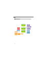
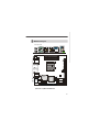
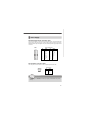
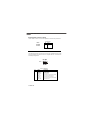
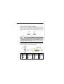
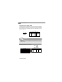
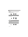
User’s Manual
Mini-ITXMMotherboard22807790
Version 1.0, August 2007
Copyrights
This manual is copyrighted and all rights are reserved. It does not allow any non authorization in
copied, photocopied, translated or reproduced to any electronic or machine readable form in
whole or in part without prior written consent from the manufacturer.
In general, the manufacturer will not be liable for any direct, indirect, special, incidental or
consequential damages arising from the use of inability to use the product or documentation, even
if advised of the possibility of such damages. The manufacturer keeps the rights in the subject to
change the contents of this manual without prior notices in order to improve the function design,
performance, quality and reliability. The author assumes no responsibility for any errors or
omissions, which may appear in this manual, nor does it make a commitment to update the
information contained herein.
Trademarks
Intel is a registered trademark of Intel Corporation.
Award is a registered trademark of Award Software, Inc.
All other trademarks, products and or product's name mentioned herein are mentioned for
identification purposes only, and may be trademarks and/or registered trademarks of their
respective companies or owners.
Safety Instructions
1.
Always read the safety instructions carefully.
2.
Keep this User’s Manual for future reference.
3.
Keep this equipment away from humidity.
4.
Lay this equipment on a reliable flat surface before setting it up.
5.
The openings on the enclosure are for air convection hence protects the equipment from overheating. DO NOT COVER THE OPENINGS.
6.
Make sure the voltage of the power source and adjust properly 110/220V before connecting the equipment to the power inlet.
7.
Place the power cord such a way that people can not step on it. Do not place
anything over the power cord.
8.
Always Unplug the Power Cord before inserting any add-on card or module.
9.
All cautions and warnings on the equipment should be noted.
10. Never pour any liquid into the opening that could damage or cause electrical
shock.
11. If any of the following situations arises, get the equipment checked by service
personnel:
† The power cord or plug is damaged.
† Liquid has penetrated into the equipment.
† The equipment has been exposed to moisture.
† The equipment does not work well or you can not get it work according to
User’s Manual.
† The equipment has dropped and damaged.
† The equipment has obvious sign of breakage.
12. DO NOT LEAVE THIS EQUIPMENT IN AN ENVIRONMENT UNCONDITIONED, STORAGE TEMPERATURE ABOVE 600 C (1400F), IT MAY DAMAGE THE EQUIPMENT.
CAUTION: Dan g er of exp losion if b attery is in correctl y rep laced .
Replace on ly with the same or equivalent type recommen ded by the
manufacturer.
iii
FCC-B Radio Frequency Interference Statement
Th is eq u ip men t h as been
tested and found to comply
with the limits for a Class B
digital device, pursuant to Part
15 of the FCC Rules. These limits are designed to provide reasonable protection
against harmful interference in a residential installation. This equipment generates,
uses and can radiate radio frequency energy and, if not installed and used in accordance with the instructions, may cause harmful interference to radio communications.
However, there is no guarantee that interference will not occur in a particular
installation. If this equipment does cause harmful interference to radio or television
reception, which can be determined by turning the equipment off and on, the user is
encouraged to try to correct the interference by one or more of the measures listed
bel ow.
† Reorient or relocate the receiving antenna.
† Increase the separation between the equipment and receiver.
† Connect the equipment into an outlet on a circuit different from that to
which the receiver is connected.
† Consult the dealer or an experienced radio/television technician for help.
Notice 1
The changes or modifications not expressly approved by the party responsible for
compliance could void the user’s authority to operate the equipment.
Notice 2
Shielded interface cables and A.C. power cord, if any, must be used in order to
comply with the emission limits.
VOIR LA NOTICE D’INSTALLATION AVANT DE RACCORDER AU RESEAU.
2807790
This device complies with Part 15 of the FCC Rules. Operation is subject to the
following two conditions:
(1) this device may not cause harmful interference, and
(2) this device must accept any interference received, including interference that
may cause undesired operation.
iv
CONTENTS
Technical Support ................................................................................................. ii
Safety Instructions ................................................................................................ iii
FCC-B Radio Frequency Interference Statement ................................................... iv
WEEE (Waste Electrical and Electronic Equipment) Statement ................................ v
Chapter 1 Product Overview .......................................................................... 1-1
Mainboard Specifications ............................................................................. 1-2
Block Diagram ............................................................................................... 1-4
Mainboard Layout ........................................................................................ 1-5
Powre Consumption .................................................................................... 1-6
Safety Compliance & MTBF .......................................................................... 1-7
Board Dimension .......................................................................................... 1-8
Back Panel & I/O Shield Drawing .................................................................. 1-9
Chapter 2 Hardware Setup ............................................................................. 2-1
Quick Components Guide ............................................................................. 2-2
Memory ....................................................................................................... 2-3
CPU (Central Processing Unit) ...................................................................... 2-4
Power Supply .............................................................................................. 2-7
Back Panel ................................................................................................... 2-8
Connectors ................................................................................................ 2-10
Jumpers ..................................................................................................... 2-16
Slots .......................................................................................................... 2-17
Chapter 3 System Resources ....................................................................... 3-1
Watch Dog Timer Setting .............................................................................. 3-2
AMI POST Code ........................................................................................... 3-3
Resource List .............................................................................................. 3-6
viii
2807790 Mainboard
Mainboard Specifications
Processor Support
- AMD Sempron ,Athlon 64/64 X2 (Dual Core) processor with AM2
package
- 4-pin CPU fan pinheader with Smart Fan Speed Control
Supported FSB
- Hyper Transport supporting speed up to 1 GHz (2000MT/s)
Chipset
- Northbridge : AMD RS690T
- Southbridge : AMD SB600
Memory Support
- DDR2 400/533/667/800 (4GB Max)
- 2 DDR2 SO-DIMM slots (unbuffered)
LAN
- 2 PCI-E Gb LAN by Marvell 88E8056
Audio
- Realtek ALC888 7.1-channel HDA codec
- 6 watt amplifier
IDE
- 1 40-pin IDE connector
- Supports 2 IDE devices
SATA
- 2 SATA II ports by SB600
- Supports storage and data transfers at up to 300MB/s
Expansion Slots
- 1 PCI slot
- 1 Mini PCI-E socket
1-2
Product Overview
Connectors
Rear I/O
- 1 PS/2 mouse port
- 1 PS/2 keyboard port
- 2 COM ports
- 1 VGA/ HDMI stack connector
- 4 USB ports
- 5 flexible audio jacks
- 1 optical SPDIF-out jack
Onboard Connector
- 2 USB connectors (4 ports)
- 1 parallel port connector (LPT)
- 1 LVDS connector
- 1 TV-Out connector
- 1 amplifier connector
- 1 front panel connector
- 1 SMBUS connector
- 1 CPU fan connector
- 1 system fan connector
- 2 SATA connectors
- 1 Chassis Intrusion connector
Form Factor
- Mini-ITX (17.0cm X17.0cm)
Mounting
- 4 mounting holes
Environmental
Operating Temperature
- Temperature: -10oC ~ 70oC
- Humidity: 0% ~ 85% RH
Storage Temperature
- Temperature: -20oC ~ 80oC
- Humidity: 25% ~ 90% RH
1-3
2807790 Mainboard
Block Diagram
1-4
Product Overview
Mainboard Layout
Backpanel I/O
DIMM 2
J2
J1
JPW1
Top : mouse
Botto m:
keyboard
DIMM 1
ATX1
COM Ports
Top: LAN Jack
Bottom : USB por ts
BATT
+
JAUD1
SB600
JTV1
J USB 2
J USB 1
PCI1
JCASE1
SATA1
SATA2
JBAT1
JLDVS1
AMD
RS690T
AL C888
T: Line-I n/ S S-Out
M: L ine-Out
B: Mic
T:RS-Out
M:CS -Out
B:SPDIF Out
J3
Wi nbond
W83627DHG
JLPT1
To p: VGA Port
Bottom : HDMI
IDEB1
J4
Top: LAN Jack
Bottom : USB por ts
CON1
JFP1 CPUFAN1 SYSFAN1
(2807790 v1.X) Mini ITX Mainboard
1-5
2807790 Mainboard
Power Consumption
Component
CPU
DDR2
HDD
ODD
Description
AMD Athlon™ 64 x2 Dual Core 2G
1024MB DDR2 533 *2
Maxtor 80G2807790
NEC DVD-Multi Record ND-4550A
12Vp
AMD ThermNow! Utility
Particle Fuly + VCD + Xcopy
3Dmark 2005
Idle
S3
1-6
12V
4.2
3.07
2.81
0.82
0
0.81
1.01
0.84
0.81
0
5V
3.03
4.66
4.27
3.09
0
3.3V
1.08
1.07
1.06
1.17
0
5VSB
0.032
0.039
0.04
0.024
0.512
-12V
0.028
0.02
0.042
0.017
0
W
79.33
76.226
69.352
39.195
2.56
Product Overview
Safety compliance & MTBF
Safety compliance
Certification
CE
RFI
EN 6100-3-2:2000 Class D
EN 6100-3-3:1995+A1:2001
Immunity EN 55024:1998+A1:2001+A2:2003
BSMI
CNS 13438 乙類(2006年版)
C-Tick
AS/NZS CISPR 22:2004
FCC
VCCI
Title of standard
Standard number
EN 55022:1998+A1:2000+A2:2003 Class B
Product family standard
Limits for harmonic current
emission
Limitation of voltage fluctuation
and flicker in low-voltage supply
system
Product family standard
FCC CFR Title 47 Part 15 Subpart B: 2005 Class B
CISPR 22: 2005
VCCI V-3:2004, Class B
VCCI V-4:2004, Class B
MTBF - Reliability Prediction
Calculation
Operation
Operating
Model
temperature(°C)
Environment
Telcordia Issue 1
35
GF, GU - Ground
Duty Cycle
MTBF(hr.)
100%
93,411
100%
52,174
Fixed,
Uncontrolled
Telcordia Issue 1
55
GF, GU - Ground
Fixed,
Uncontrolled
1-7
2807790 Mainboard
Board Dimension
1-8
Product Overview
Back Panel & I/O Shield Drawing
1-9
Hardware Setup
Chapter 2
Hardware Setup
This chapter provides you with the information about
hardware setup procedures. While doing the installation,
be careful in holding the components and follow the
installation procedures. For some components, if you
install in the wrong orientation, the components will not
work properly.
Use a grounded wrist strap before handling computer
comp onen ts. Static el ectricity may damag e th e
components.
2-1
2807790 Mainboard
Quick Components Guide
Back Panel,
p.2-8
DIMM1~2,
p.2-3
J1~J2,
p.2-16
CPU,
p.2-4
J4, p.2-15
JPW1,
p.2-7
ATX1,
p.2-7
IDEB1, p.2-10
J3, p.2-16
SATA1~2,
p.2-11
JLVDS1,
p.2-15
JLPT1, p.2-13
JAUD1, p.2-12
JCASE1,
p.2-11
Mini PCIE, p.2-17
PCI1, p.2-17
SYSFAN1, p.2-13
CPUFAN1, p.2-13
JUSB1~2, p.2-14
JTV1, p.2-14
2-2
JFP1, p.2-12
JBAT1,
p.2-16
Hardware Setup
Memory
The mainboard provides two 200-pin unbuffered DDR2 400/533/667/800 SO-DIMM
slots and supports up to 4GB system memory.
DIMM2
200-pin, unbuffered
DIMM1
200-pin, unbuffered
Installing Memory Modules
1. The memory module has only one notch on the center and will only fit in the right
orientation.
2. Insert the memory module vertically into the SO-DIMM slot. Then push it in until the
golden finger on the memory module is deeply inserted in the SO-DIMM slot.
Important
You can barely see the golden finger if the memory module is properly inserted
in the DIMM slot.
3. The clip at each side of the SO-DIMM slot will automatically close.
Important
To ensure the installations of memory and CPU successfully, please note that
to insert the memory modules first before install CPU and cooler set. And
please always insert the memory module into the DIMM2 first.
2-3
2807790 Mainboard
CPU (Central Processing Unit)
The mainboard supports AMD® Athlon64/ 64x2 & Sempron processors. The mainboard
uses a CPU socket called Socket AM2 for easy CPU installation. When you are
installing the CPU, make sure the CPU has a heat sink and a cooling fan
attached on the top to prevent overheating. If you do not have the heat sink and
cooling fan, contact your dealer to purchase and install them before turning on the
computer.
Important
Overheating
Overheating will seriously damage the CPU and system. Always make sure
the cooling fan can work properly to protect the CPU from overheating. Make
sure that you apply an even layer of thermal paste (or thermal tape) between
the CPU and the heatsink to enhance heat dissipation.
Replaceing the CPU
While replacing the CPU, always turn off the ATX power supply or unplug the
power supply’s power cord from the grounded outlet first to ensure the safety
of CPU.
2-4
Hardware Setup
CPU Installation Procedures for Socket AM2
1. Please turn off the power and
unplug the power cord before
installing the CPU.
2. Pull the lever sideways away
from the socket. Make sure to
raise the lever up to a 90-degree angle.
3. Look for the gold arrow of the
CPU. The gold arrow shou ld
point as shown in the picture.
The CPU can only fit in the correct orientation.
4. If the CPU is correctly installed,
the pins should be completely
embedded into the socket and
can not be seen. Please note
that any violation of the correct
instal l ation p roced u res may
cause permanent damages to
your mainboard.
Op en Lev er
Slid ing
Pla te
90 de gree
Go ld ar row
C orrec t CP U pla cem en t
G o ld ar row
O
In corr e ct C PU plac e ment
G old arr ow
5. Press the CPU down firmly into
the socket and close the lever.
As the CPU is likely to move while
the lever is bein g closed, always close the lever with your
fingers pressing tightly on top of
the CPU to make sure the CPU is
properly and completely embedded into the socket.
P re ss d ow n
the CP U
Cl ose
Le ve r
2-5
2807790 Mainboard
Installing AMD Socket AM2 CPU Cooler Set
When you are installing the CPU, make sure the CPU has a heat sink and a
cooling fan attached on the top to prevent overheating. If you do not have the
heat sink and cooling fan, contact your dealer to purchase and install them before
turning on the computer.
Important
Mainboard photos shown in this section are for demonstration of the cooler
installation for Socket AM2 CPUs only. The appearance of your mainboard
may vary depending on the model you purchase.
1. Position the cooling set onto the retention mechanism.
Hook one end of the clip to hook
first.
2. Then press down the other end of
the clip to fasten the cooling set on
the top of the retention mechanism.
Locate the Fix Lever and lift up it .
Fixed Lever
3. Fasten down the lever.
2-6
4. Attach the CPU Fan cable to the CPU
fan connector on the mainboard.
Hardware Setup
Power Supply
ATX 20-Pin System Power Connector: ATX1
This connector allows you to connect to an ATX power supply. To connect to the ATX
power supply, make sure the plug of the power supply is inserted in the proper
orientation and the pins are aligned. Then push down the power supply firmly into the
connector.
ATX1 Pin Definition
ATX1
10 20
PIN
SIGNAL
PIN
SIGNAL
1
2
3
4
5
6
7
8
9
3.3V
3.3V
GND
5V
GND
5V
GND
PW_OK
5V_SB
10
12V
11
12
13
14
15
16
17
18
19
20
3.3V
-12V
GND
PS_ON
GND
GND
GND
-5V
5V
5V
1 11
ATX 12V Power Connector: JPW1
This 12V power connector JPW1 is used to provide power to the CPU.
Pin Definition
1
3
PIN
SIGNAL
2
4
1
2
3
4
GND
GND
12V
12V
JPW1
Important
Power supply of 350watts (and above) is highly recommended for system
stability.
2-7
2807790 Mainboard
Back Panel
M ouse
Serial Port
LAN
LAN
Line-In/
SS-Out RS-Out
VGA Port
Line-Out CS-Out
Keyboard
Serial Port
USB
USB
HDMI Port
Mic-In SPDIF-Out
Mouse/Keyboard Connector
The standard PS/2® mouse/keyboard DIN connector is for a PS/2® mouse/keyboard.
Serial Port
The serial port is a 16550A high speed communications port that sends/ receives 16
bytes FIFOs. You can attach a serial mouse or other serial devices directly to the
connector.
LAN (RJ-45) Jacks
Th e st an d ar d R J- 45 j a ck s a re f or
connection to Local Area Network (LAN).
You can connect network cables to them.
Activity Indicator
Le ft LED
100M Cable Plug-in
1000M Cable Plug-in
Right LED
Active LED
100M/1000M Speed LED
Yellow
Green/Orange
No Transmission
OFF
OFF
Transition
Yellow(Blinking)
OFF
No Transmission
OFF
Green(Lighting)
Transition
Yellow(Blinking)
Green(Lighting)
No Transmission
OFF
Orange(Lighting)
Transition
Yellow(Blinking)
Orange(Lighting)
OFF
OFF
LED Color
10M Cable Plug-in
Link Indicator
In S3/S4/S5 Standby State
USB Connectors
The UHCI (Universal Host Controller Interface) Universal Serial Bus root is for attaching
USB devices such as keyboard, mouse, or other USB-compatible devices.
2-8
Hardware Setup
VGA Port
The DB15-pin female connector is provided for video monitors.
HDMI Port
The High-Definition Multimedia Interface (HDMI) is an all-digital audio/video interface
capable of transmitting uncompressed streams. HDMI supports all TV format, including
standard, enhanced, or high-definition video, plus multi-channel digital audio on a
single cable.
Audio Port Connectors
These audio connectors are used for audio devices. You can differentiate the color
of the audio jacks for different audio sound effects.
Line-In/ SS-Out (Blue) - Line In / Side-Surround Out in 7.1 channel mode,
is used for external CD player, tapeplayer or other
audio devices.
Line-Out (Green) - Line Out, is a connector for speakers or headphones.
Mic (Pink) - Mic, is a connector for microphones.
RS-Out (Black) - Rear-Surround Out in 4/ 5.1/ 7.1 channel mode.
CS-Out (Orange) - Center/ Subwoofer Out in 5.1/ 7.1 channel mode.
Optical S/PDIF-Out connector
This SPDIF (Sony & Philips Digital Interconnect Format) connector is provided for
digital audio transmission to external speakers through a fiber cable.
2-9
2807790 Mainboard
Connectors
IDE Connector: IDEB1
The mainboard has a 32-bit Enhanced PCI IDE and Ultra DMA 33/66/100/133 controller
that provides PIO mode 0~4, Bus Master, and Ultra DMA 33/66/100/133 function. You
can connect hard disk drives, CD-ROM and other IDE devices.
The Ultra ATA133 interface boosts data transfer rates between the computer and the
hard drive up to 133 megabytes (MB) per second.
IDEB1
Important
If you install two IDE devices, you must configure the second drive to Slave
mode by setting its jumper. Refer to the hard disk documentation supplied by
hard disk vendors for jumper setting instructions.
2-10
Hardware Setup
Serial ATA Connectors: SATA1, SATA2
SATA1~SATA2 are high-speed SATA interface ports and support SATA data rates of
300MB/s. Each SATA connector can connect to 1 hard disk device and is fully compliant
with Serial ATA 2.0 specifications.
SATA1
SATA2
Important
Please do not fold the Serial ATA cable into 90-degree angle. Otherwise,
data loss may occur during transmission.
Chassis Intrusion Connector: JCASE1
This connector connects to the chassis intrusion switch cable. If the chassis is
opened, the chassis intrusion mechanism will be activated. The system will record
this status and show a warning message on the screen. To clear the warning, you
must enter the BIOS utility and clear the record.
1
2
CINTRU
GND
JCASE1
2-11
2807790 Mainboard
Audio Amplifier Connector: JAUD1
The 6W JAUD1 is used to connect audio amplifiers to enhance audio performance.
Pin Definition
PIN
JAUD1
1
SIGNAL
1
AMP_R+
2
AMP_R-
3
AMP_L+
4
AMP_L-
Front Panel Connector: JFP1
The mainboard provides one front panel connector for electrical connection to the
front panel switches and LEDs. The JFP1 is compliant with Intel® Front Panel I/O
Connectivity Design Guide.
+
-
Power Power
LED Switch
10
9
2
1
+
+
JFP1
HDD Reset
LED Switch
JFP1 Pin Definition
2-122807790
PIN
SIGNAL
DESCRIPTION
1
2
3
4
5
6
7
8
9
HD_LED +
FP PWR/SLP
HD_LED FP PWR/SLP
RST_SW PWR_SW +
RST_SW +
PWR_SW RSVD_DNU
Hard disk LED pull-up
Power LED pull-up
Hard disk active LED
Power LED pull-up
Reset Switch low reference pull-down to GND
Power Switch high reference pull-up
Reset Switch high reference pull-up
Power Switch low reference pull-down to GND
Reserved. Do not use.
Hardware Setup
Fan Power Connectors: CPUFAN1, SYSFAN1
CPUFAN1
GND
+1 2V
SENSOR
GND
+1 2V
SENSOR
Control
The fan power connectors support system cooling fan with +12V. When connecting
the wire to the connectors, always take note that the red wire is the positive and
should be connected to the +12V, the black wire is Ground and should be connected
to GND. If the mainboard has a System Hardware Monitor chipset on-board, you must
use a specially designed fan with speed sensor to take advantage of the CPU fan
control.
SYSFAN1
Important
Please refer to the recommended CPU fans at A D’s official website or consult
the vendors for proper CPU cooling fan.
Parallel Port Header: JLPT1
The mainboard provides a 26-pin header for connection to an optional parallel port
bracket. The parallel port is a standard printer port that supports Enhanced Parallel
Port (EPP) and Extended Capabilities Parallel Port (ECP) mode.
26 25
Parallel Port
Bracket (Optional)
JLPT1
2 1
PIN
SIGNAL
PIN
SIGNAL
PIN
SIGNAL
PIN
SIGNAL
1
RSTB#
2
AFD#
15
PRND6
16
GND
3
5
7
9
11
13
PRND0
PRND1
PRND2
PRND3
PRND4
PRND5
4
6
8
10
12
14
ERR#
PINIT#
LPT_SLIN#
GND
GND
GND
17
19
21
23
25
PRND7
ACK#
BUSY
PE
SLCT
18
20
22
24
26
GND
GND
GND
GND
GND
2-13
2807790 Mainboard
Front USB Connector: JUSB1/ JUSB2
The USB 2.0 pinheader is compliant with Intel® I/O Connectivity Design Guide. USB 2.
0 technology increases data transfer rate up to a maximum throughput of 480Mbps,
which is 40 times faster than USB 1.1, and is ideal for connecting high-speed USB
interface peripherals such as USB HDD, digital cameras, MP3 players, printers,
modems and the like.
Pin Definition
2
10
9
1
JUSB1/ 2
PIN
SIGNAL
PIN
SIGNAL
1
VCC
2
VCC
3
USB0-
4
USB1-
5
USB0+
6
USB1+
7
GND
8
GND
9
Key (no pin)
10
NC
Important
Note that the pins of VCC and GND must be connected correctly to avoid
possible damage.
TV-Out Connector: JTV1
3
The mainboard provides a TV-Out connector.
JTV1
41
JTV1 Pin Definition
CRT
HDMI
LVDS
TV OUT
Display Matrix
HDMI
LVDS
X
CRT
X
V
X
V
X
V : Support
TV OUT
V
V
V
X : No Support
2-1428077902807790
X
X
V
Pin
Description
Pin
Description
1
GND
2
Y_L
3
C_L
4
COMP_L
5
GND
6
Key (no pin )
Hardware Setup
LVDS Flat Panel Connector: JLVDS1
The LVDS (Low Voltage Differential Signal)
connector provides a digital interface typically
used with flat panels. After connecting an
LVDS interfaced flat panel to the JLVDS1, be
sure to check the panel datasheet and set the
J1 LVDS Power Selection Jumper to a proper
voltage.
CRT
X
CRT
HDMI
X
V
X
LVDS
TV OUT
1
40
2
JLVDS1
V
X
V : Support
SIGNAL
39
Display Matrix
HDMI
LVDS
PIN
TV OUT
V
V
X
X
V
V
X : No Support
SIGNAL
+12V
2
1
+12V
+12V
4
3
+12V
GND
6
5
+12V
GND
8
7
VCC3/VCC5
LCD_VDD
10
9
LCD_VDD
LDDC_DATA
12
11
LDDC_CLK
LVDS_VDDEN
14
13
L_BKLTCTL
GND
16
15
L_BKLTEN
LA_DATA0
18
17
LA_DATA0#
LA_DATA1
20
19
LA_DATA1#
LA_DATA2
22
21
LA_DATA2#
LA_CLK
24
23
LA_CLK#
LA_DATA3
26
25
LA_DATA3#
GND
28
27
GND
LB_DATA0
30
29
LB_DATA0#
LB_DATA1
32
31
LB_DATA1#
LB_DATA2
34
33
LB_DATA2#
LB_CLK
36
35
LB_CLK#
LB_DATA3
38
37
LB_DATA3#
GND
40
39
GND
I2C Bus Connector: J4
The mainboard provides one I2C (also known as I2C) Bus connector for users to
connect System Management Bus (SMBus) interface.
Pin Definition
J4
Pin
Signal
4
1
VCC5F
1
2
SMBCLK
3
GND
4
SMBDATA
2-15
2807790 Mainboard
Jumpers
COM Port Power Jumpers: J1, J2
These jumpers specify the operation voltage of the onboard serial ports.
1
1
1
J2
J1
+12V
+5V
Clear CMOS Jumper: JBAT1
There is a CMOS RAM onboard that has a power supply from external battery to keep
the data of system configuration. With the CMOS RAM, the system can automatically
boot OS every time it is turned on. If you want to clear the system configuration, set
this jumper to clear data.
1
1
3
3
1
JBAT1
Keep Data
Clear Data
Important
You can clear CMOS by shorting 2-3 pin while the system is off. Then return
to 1-2 pin position. Avoid clearing the CMOS while the system is on; it will
damage the mainboard.
LVDS Power Selection Jumper: J3
Use this jumper to specify the operation voltage of the LVDS interfaced flat panel.
1
+3V
2-162807790
1
1
J3
+5V
Hardware Setup
Slots
Mini PCI (Peripheral Component Interconnect) Express Slot
The CON1 is Mini PCI-E connector for wireless LAN, TV tuner, and Robson NAND
Flash.
Mini PCI-E Slot
PCI (Peripheral Component Interconnect) Slot
The PCI slot supports LAN card, SCSI card, USB card, and other add-on cards that
comply with PCI specifications.
32-bit PCI Slot
PCI Interrupt Request Routing
The IRQ, acronym of interrupt request line and pronounced I-R-Q, are hardware lines
over which devices can send interrupt signals to the microprocessor. The PCI IRQ
pins are typically connected to the PCI bus pins as follows:
DEVICE
IDSEL
INT A
INTB
INTC
INTD
REQ# / GNT#
32-bit PCI Slot
AD18
E
F
G
H
REQ#0 / GNT#0
Important
When adding or removing expansion cards, make sure that you unplug the
power supply first. Meanwhile, read the documentation for the expansion card
to configure any necessary hardware or software settings for the expansion
card, such as jumpers, switches or BIOS configuration.
2-17
System Resources
Chapter 3
System Resources
This chapter provides information on the following
system resources:
1. Watch Dog Timer Setting (p. 3-2)
2. AMI POST Code (p. 3-3)
3. Resource List (p. 3-6)
3-1
2807790 Mainboard3
Watch Dog Timer Setting
Software code
SIO_IDX equ 4EH
SIO_DTA equ 4FH
Timer equ 10; reset after 10 seconds
1. Enter configuration mode
mov dx,SIO_IDX
mov al,87h
out dx,al
out dx,al
2. Set to LDN 08
mov dx,SIO_IDX
mov al,07h
out dx,al
mov dx,SIO_DTA
mov al,08h
out dx,al
3. Set WatchDog Timer
mov dx,SIO_IDX
mov al,0f6h
out dx,al
mov dx,SIO_DTA
mov al,Timer
out dx,al
4. Exit configuration mode
mov dx,SIO_IDX
mov al,0AAh
out dx,al
3-2
System Resources
AMI POST Code
Bootblock Initialization Code Checkpoinits
The Bootblock initialization code sets up the chipset, memory and other components
before system memory is available. The following table describes the type of checkpoints that may occur during the bootblock initialization portion of the BIOS:
Bootblock Initialization Code Checkpoint list
Checkpoint
Before D1
D1
DO
D2
D3
D4
D5
D6
D7
D8
D9
DA
Description
Early chipset initialization is done. Early super I/O initialization is done
including RTC and keyboard controller. NMI is disabled.
Perform keyboard controller BAT test. Check if waking up from power
management suspend state. Save power-on CPUID value in scratch
CMOS.
Go to flat mode with 4GB limit and GA20 enabled. Verify the bootblock
checksum.
Disable CACHE before memory detection. Execute full memory sizing
module. Verify that flat mode is enabled.
If memory sizing module not executed, start memory refresh and do
memory sizing in Bootblock code. Do additional chipset initialization.
Re-enable CACHE. Verify that flat mode is enabled.
Test base 512KB memory. Adjust policies and cache first 8MB. Set stack.
Bootblock code is copied from ROM to lower system memory and control is
given to it. BIOS now executes out of RAM.
Both key sequence and OEM specific method is checked to determine if
BIOS recovery is forced. Main BIOS checksum is tested. If BIOS recovery
is necessary, control flows to checkpoint E0.
Restore CPUID value back into register. The Bootblock- Runtime interface
module is moved to system memory and control is given to it. Determine
whether to execute serial flash
The Runtime module is uncompressed into memory. CPUID information is
stored in memory.
Store the Uncompressed pointer for future use in PMM. Copying Main
BIOS into memory. Leaves all RAM below 1MB Read-Write including E000
and F000 shadow areas but closing SMRAM.
Restore CPUID value back into register. Give control to BIOS POST
(ExecutePOSTKernel.) See POST Code Checkpoint list for more
information.
3-3
2807790 Mainboard
Post Code Checkpoints
The POST code checkpoints are the largest set of checkpoints during the BIOS
preboot process. The following table describes the type of checkpoints that may
occur during the POST portion of the BIOS:
Checkpoint
Description
03
Disable NMI, Parity, video for EGA, and DMA controllers. Initialize BIOS,
POST, Runtime data area. Also initialize BIOS modules on POST entry
and GPNV area. Initialized CMOS as mentioned in the Kernel Variable
“Wcomsflags”.
Check CMOS diagnostic byte to determine if battery power is OK and
CMOS checksum is OK. Verify CMOS checksum manually by reading
storage area. If the CMOS checksum is bad, update CMOS with
power-on default values and clear passwords. Initialize status register A.
Initializes data variables that are based on CMOS setup questions.
Initializes both the 8259 compatible PICs in the system.
Initializes the interrupt controlling hardware (generally PIC) and interrupt
vector table.
Do R/W test to CH-2 count reg. Initialize CH-0 as system timer. Install the
POSTINT1Ch handler. Enable IRQ-0 in PIC for system timer interrupt.
Traps INT1Ch vector to “POSTINT1ChHandlerBlock”.
Initializes the CPU. The BAT test is being done on KBC.
Program the keyboard controller command byte is being done after Auto
detection of KB/MS using AMI KB-5.
Initializes the 8042 compatible Key Board Controller.
Detects the presence of PS/2 mouse.
Detects the presence of keyboard in KBC port.
Testing and initialization of different Input Devices. Also, update the
Kernel Variables.
Traps the INT09h vector, so that the POST INT09h handler gets control
for IRQ1. Uncompress all available language, BIOS logo, and Silent logo
modules.
Early POST initialization of chipset registers.
Uncompress and initialize any platform specific BIOS modules.
Initialize System Management Interrupt.
Initializes different devices through DIM.
Initializes different devices. Detects and initializes the video adapter
installed in the system that have optional ROMs.
Initializes all the output devices.
Allocate memory for ADM module and uncompress it. Give control to
ADM module for initialization. Initialize language and font modules for
ADM. Activate ADM module.
Initializes the silent boot module. Set the window for displaying test
information.
Displaying sign-on message, CPU information, setup key message, and
any OEM specific information.
04
05
06
08
0A
0B
0C
0E
13
24
30
2A
2C
2E
31
33
37
3-4
System Resources
Checkpoint
Description
38
39
3A
3B
Initializes different devices through DIM.
Initializes DMAC-1 & DMAC-2.
Initializes RTC date/time.
Test for total memory installed in the system. Also, Check for DEL or ESC
keys to limit memory test. Display total memory in the system.
Mid POST initialization of chipset registers.
Detect different devices (Parallel ports, serial ports, and coprocessor in
CPU…etc.)successfully installed in the system and update the BDA,
EBDA…etc.
Programming the memory hole or any kind of implementation that needs
an adjustment in system RAM size if needed.
Updates CMOS memory size from memory found in memory test.
Allocates memory for Extended BIOS Data Area from base memory.
Initializes NUM-LOCK status and programs the KBD typematic rate.
Initialize Int-13 and prepare for IPL detection.
Initializes IPL devices controlled by BIOS and option ROMs.
Initializes remaining option ROMs.
Generate and write contents of ESCD in NVRam.
Log errors encountered during POST.
Display errors to the user and gets the user response for error.
Execute BIOS setup if needed / requested.
Late POST initialization for chipset registers.
Program the peripheral parameters. Enable / Disable NMI as selected.
Late POST initialization of system management interrupt.
Check boot password if installed.
Clean-up work needed before booting to OS.
Takes care of runtime image preparation for different BIOS modules Fill the
free area in F000h segment with 0FFh.
Initializes the Microsoft IRQ Routing Table. Prepares the runtime language
module. Disables the system configuration display if needed.
Initialize runtime language module.
Displays the system configuration screen if enabled. Initialize the CPU’s
before boot, which includes the programming of the MTRR’s.
Prepare CPU for OS boot including final MTRR values.
Wait for user input at config display if needed.
Uninstall POST INT1Ch vector and INT09h vector. Deinitializes the ADM
module.
Prepare BBS for 19 boot.
End of POST initialization of chipset registers.
Save system contest for ACPI.
Passes control to OS Loader (typically INT19h).
3C
40
50
52
60
75
78
7A
7C
84
85
87
8C
8E
90
A0
A1
A2
A4
A7
A8
A9
AA
AB
AC
B1
00
3-5
2807790 Mainboard
Resource List
SB600 GPIO Config.
G PIO Pi n
GPIO0
GPIO1
GPIO2
GPIO3
GPIO4
GPIO5
GPIO6
GPIO7
GPIO8
GPIO9
GPIO10
GPIO11
GPIO12
GPIO13
GPIO14
GPIO[ 15..30 ]
GPIO31
GPIO32
GPIO33
GPIO34
GPIO35
GPIO36
GPIO37
GPIO38
GPIO39
GPIO40
GPIO41
GPIO42
GPIO43
GPIO44
GPIO45
GPIO46
GPIO47
GPIO48
GPIO49
GPIO50
GPIO51
GPIO52
GPIO[ 53..60 ]
GPIO61
GPIO62
GPIO63
GPIO64
GPIO65
GPIO66
GPIO67
GPIO68
GPIO69
GPIO70
GPIO71
GPIO72
GPIO73
3-6
Type
Multiplexed
Power
I/OD(3.3V)
I/O(3.3V)
I/O(3.3V)
I/O(3.3V)
I/O(3.3V)
I/O(3.3V)
I/OD(3.3V)
I/O(3.3V)
I/O(3.3V)
I/O(3.3V)
I/O(3.3V)
I/O(S5_3.3V)
I/O(S5_3.3V)
O(3.3V)
I/O(3.3V)
I/O(3.3V)
I/O(S5_3.3V)
I/O(S5_3.3V)
I/O(3.3V)
I/O(3.3V)
I/O(3.3V)
I/O(3.3V)
I/O(3.3V)
I/O(3.3V)
I/O(3.3V)
I/O(3.3V)
I/O(3.3V)
I/O(S5_3.3V)
I/O(S5_3.3V)
I/O(S5_3.3V)
I/O(S5_3.3V)
I/O(S5_3.3V)
I/O(S5_3.3V)
I/O(3.3V)
I/O(3.3V)
I/O(3.3V)
I/O(3.3V)
I/O(3.3V)
I/O(3.3V)
I/O(3.3V)
I/O(3.3V)
I/O(3.3V)
I/O(3.3V)
I/O(3.3V)
I/O(S5_3.3V)
OD(3.3V)
I/O(3.3V)
I/O(S5_3.3V)
I/O(3.3V)
I/O(3.3V)
I/O(3.3V)
I/O(3.3V)
NA
NA
NA
NA
NA
NA
NA
NA
NA
NA
NA
SPI_D O
SPI_DI
NA
NA
IDE_D [ 0..15 ]
SPI_HO LD#
SPI_CS#
IN TE#
IN TE#
IN TE#
IN TE#
NA
NA
AC_SDOUT
NA
NA
ACZ_SDIN0
NA
NA
NA
NA
SPI_CLK
NA
NA
NA
NA
NA
NA
NA
NA
NA
TALERT#
BM REQ#
NA
SATA_ACT#
NA
NA
NA
NA
NA
NA
M ain
M ain
M ain
M ain
M ain
M ain
M ain
M ain
M ain
M ain
M ain
Standby
Standby
M ain
M ain
M ain
Standby
Standby
M ain
M ain
M ain
M ain
M ain
M ain
M ain
M ain
M ain
Standby
Standby
Standby
Standby
Standby
Standby
M ain
M ain
M ain
M ain
M ain
M ain
M ain
M ain
M ain
M ain
M ain
Standby
M ain
M ain
VBA T
M ain
M ain
M ain
M ain
Function
NC
NC
NC
NC
NC
NC
NC
NC
NC
IDE Cable Dectec
NC
SPI_D O
SPI_D I
NC
NC
IDE_D [ 0..15 ]
SPI_H OLD#
SPI_CS#
INTE#
INTE#
INTE#
INTE#
NC
NC
A C_SDOUT#
NC
NC
A CZ_SD IN0#
NC
NC
NC
G PIO46
SPI_CLK
AMP_GAIN0
AMP_GAIN1
AMP_EN
NC
NC
NC
NC
NC
NC
TALERT#
BM REQ#
NC
SATA_ACT#
NC
NC
NC
NC
NC
NC
System Resources
SB600 GPM Config.
GP M Pi n
Type
Multiplexed
Power
GPM#0
GPM#1
GPM#2
GPM#3
GPM#4
GPM#5
GPM#6
GPM#7
GPM#8
GPM#9
I/O(S5_3.3V)
I/O(S5_3.3V)
I/O(S5_3.3V)
I/O(S5_3.3V)
I/O(S5_3.3V)
I/O/OD(S5_3.3V)
I/O(S5_3.3V)
I/O(S5_3.3V)
I/O(S5_3.3V)
I/O(S5_3.3V)
USB_OC0#
USB_OC1#
NA
NA
NA
NA
NA
SYS_RESET#
NA
NA
Standby
Standby
Standby
Standby
Standby
Standby
Standby
Standby
Standby
Standby
Function
USB OverC urrent
USB OverC urrent
NC
NC
NC
WLAN _PWRON
GPM6#
SYS_RESET#
NC
NC
SB600 EXTEVENT & GEVENT Config.
GEVENT P in
Type
Multiplexed
Power
EXTEVENT0#
EXTEVENT1#
GEVENT2#
GEVENT3#
GEVENT4#
GEVENT5#
GEVENT6#
GEVENT7#
GEVENT8#
I/O(S5_3.3V)
I/O(3.3V)
I/O(S5_3.3V)
I/O(S5_3.3V)
I/O(S5_3.3V)
I/O(S5_3.3V)
I/O(S5_3.3V)
I/O(S5_3.3V)
I/O(S5_3.3V)
NA
NA
NA
LPC_PM E#
PCI_PM E#
NA
NA
NA
PCIE_WAKE#
Standby
M ain
Standby
Standby
Standby
Standby
Standby
Standby
Standby
Function
NC
NC
NC
LPC_PME#
PCI_PME#
NC
NC
NC
PCIE_WAKE#
3-7
2807790 Mainboard
I/O Map
I/O Port
0000-000F
0020-0021
002E-002F
0040-0043
004E-004F
0060, 0064
0070-0073
0080-0090
0092
00A0-00A1
00B2-00B3
00C0-00DF
00F0-00FF
01F0-01F7
02F8-02FF
0376
0378-037F
03F6
03F8-03FF
0800-085F
0B00-0B0F
0CF8-0CFF
3-8
Description
DMA Controller 1
Interrupt Controller 1
SIO Port
ystem Timer
TPM Port
Keyboard Controller
RTC and CMOS
DMA Controller Page Registers
Port 92h
Interrupt Controller 2
APM register
DMA Controller 2
Numeric Data Processor
Primary IDE Controller
COM2
Secondary IDE Controller
LPT1
Primary IDE Controller
COM1
ACPI I/O space
SMBus I/O Space
PCI configuration Port
System Resources
PCI Devices
PCI Device
Device
Ven. ID Dev. ID
ATi Host Bridge
1002
7910
ATi PCI-to-PCI Bridge
1002
7912
ATi PCI-to-PCI Bridge
1002
7914
ATi PCI-to-PCI Bridge
1002
7915
ATi PCI-to-PCI Bridge
1002
7916
ATi IDE Controller
1002
4380
ATi OHCI USB Controller
1002
4387
ATi OHCI USB Controller
1002
4388
ATi OHCI USB Controller
1002
4389
ATi OHCI USB Controller
1002
438A
ATi OHCI USB Controller
1002
438B
ATi Unknown Deivce
1002
4386
ATi SMBus
1002
4385
ATi IDE Controller
1002
438C
ATi Unknown Deivce
1002
4383
ATi ISA Bridge
1002
438D
ATi Subtractive Decode P2P Bridge 1002
4384
AMD Host Bridge
1022
1100
Bus#
00
00
00
00
00
00
00
00
00
00
00
00
00
00
00
00
00
00
Dev#
00
01
04
05
06
12
13
13
13
13
13
13
14
14
14
14
14
18
Func#
00
00
00
00
00
00
00
01
02
03
04
05
00
01
02
03
04
00
3-9
2807790 Mainboard
SMBus Resource Allocation
SMBus Resource Allocation
Device
Address
Description
MS-6
0101 111X ACPI Controller
DIMM Slot 1010 0000 SPD
ISA Interrupt Allocation
ISA Interrupt Allocation
IRQ
Description
IRQ0
System Timer
IRQ1
Keyboard Controller
IRQ2
Cascade Interrupt
IRQ3
COM2
IRQ4
COM1
IRQ5
PCI Device
IRQ6
PCI Device
IRQ7
LPT1
IRQ8
RTC
IRQ9
ACPI Controller Interrupt
IRQ10
PCI Device
IRQ11
PCI Device
IRQ12
PS/2 Mouse
IRQ13
Numeric Data Processor
IRQ14
Primary IDE Controller
IRQ15
Secondary IDE Controller
ISA DMA Channel Allocation
3-10
Any advice or comments about our products and service, or anything we can help you
with please don’t hesitate to contact with us. We will do our best to support your products,
projects and business.
Address:
Global American, Inc.
17 Hampshire Drive
Hudson, NH 03051
Telephone: Toll Free (U.S. Only) 800-833-8999
(603)886-3900
FAX:
(603)886-4545
Website:
E-Mail:
http://www.globalamericaninc.com
[email protected]