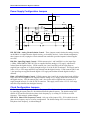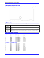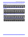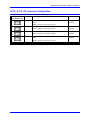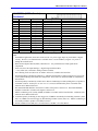
1
^1 HARDWARE MANUAL
^2 PMAC Mini PCI
^3 Programmable Multi-Axis Controller
^4 5xx-603712-xHxx
^5 April 26, 2010
Single Source Machine Control
Power // Flexibility // Ease of Use
21314 Lassen Street Chatsworth, CA 91311 // Tel. (818) 998-2095 Fax. (818) 998-7807 // www.deltatau.com
Copyright Information
© 2010 Delta Tau Data Systems, Inc. All rights reserved.
This document is furnished for the customers of Delta Tau Data Systems, Inc. Other uses are
unauthorized without written permission of Delta Tau Data Systems, Inc. Information contained in
this manual may be updated from time-to-time due to product improvements, etc., and may not
conform in every respect to former issues.
To report errors or inconsistencies, call or email:
Delta Tau Data Systems, Inc. Technical Support
Phone: (818) 717-5656
Fax: (818) 998-7807
Email: [email protected]
Website: http://www.deltatau.com
Operating Conditions
All Delta Tau Data Systems, Inc. motion controller products, accessories, and amplifiers contain
static sensitive components that can be damaged by incorrect handling. When installing or handling
Delta Tau Data Systems, Inc. products, avoid contact with highly insulated materials. Only
qualified personnel should be allowed to handle this equipment.
In the case of industrial applications, we expect our products to be protected from hazardous or
conductive materials and/or environments that could cause harm to the controller by damaging
components or causing electrical shorts. When our products are used in an industrial environment,
install them into an industrial electrical cabinet or industrial PC to protect them from excessive or
corrosive moisture, abnormal ambient temperatures, and conductive materials. If Delta Tau Data
Systems, Inc. products are directly exposed to hazardous or conductive materials and/or
environments, we cannot guarantee their operation.
REVISION HISTORY
REV.
1
DESCRIPTION
REVISIONS TO FLEX CPU BAUD RATE, PPS. 6 &21
DATE
CHG
APPVD
05/09/06
CP
S. SATTARI
2
UPDATED ENCODER SETTING DESC., PPS. 6 & 20
01/30/09
CP
S. MILICI
3
CORRECTED JUMPER LAYOUT E85-E87-E88, P. 25
04/26/10
CP
S. MILICI
PMAC Mini PCI Hardware Reference Manual
Table of Contents
INTRODUCTION .....................................................................................................................................................1
Features ...................................................................................................................................................................1
Dimensions..............................................................................................................................................................2
HARDWARE SETUP ...............................................................................................................................................3
Board Configuration................................................................................................................................................3
Base Version .......................................................................................................................................................3
Option 2: Dual-Ported RAM .............................................................................................................................3
Option 5xF: CPU Speed Options .......................................................................................................................3
Option 6: Extended Servo Algorithm Firmware................................................................................................4
Option 6L: Special Lookahead Firmware .........................................................................................................4
Option 8A: High-Accuracy Clock Crystal .........................................................................................................4
Option 10: Firmware Version Specification.......................................................................................................4
Option 15: V-to-F Converter for Analog Input ..................................................................................................4
General Purpose Digital Inputs and Outputs (JOPTO Port) .............................................................................4
Power Supply Configuration Jumpers.....................................................................................................................5
Clock Configuration Jumpers..................................................................................................................................5
Encoder Configuration Jumpers..............................................................................................................................6
Single-Ended Encoders.......................................................................................................................................6
Differential Encoders..........................................................................................................................................6
Board Reset/Save Jumpers ......................................................................................................................................7
Communication Jumpers.........................................................................................................................................7
Reserved Configuration Jumpers ............................................................................................................................7
I/O Configuration Jumpers......................................................................................................................................7
Resistor Pack Configuration: Termination Resistors .............................................................................................8
The Optional Dual-Ported RAM .............................................................................................................................9
LED Indicators ........................................................................................................................................................9
Input and Output Mapping ......................................................................................................................................9
Y:$FFC0 J1 (JDISP) Outputs ..........................................................................................................................9
Y:$FFC1 J3 (JTHW) Inputs .............................................................................................................................9
Y:$FFC2 J3 (JTHW) Outputs ........................................................................................................................10
Y:$FFC3 J5 (JOPTO) Inputs .........................................................................................................................10
Y:$FFC4 J5 (JOPTO) Outputs ......................................................................................................................10
Y:$FFC5 Dedicated Use................................................................................................................................10
Y:$FFC6 Dedicated Use................................................................................................................................10
OPTION 15 — VOLTAGE TO FREQUENCY CONVERTER .........................................................................12
Configuration as Analog Input with a 0-100 kHz Frequency Range ...............................................................12
Configuration as Analog Input with a 0-2 MHz Frequency Range..................................................................13
General Configuration for Step and Direction Outputs ...................................................................................13
0-100 kHz Frequency Range and Pseudo-Feedback (no External Encoder Connected) .................................14
0-2 MHz Frequency Range and Pseudo-Feedback (no External Encoder Connected) ...................................14
0-100 kHz Frequency Range and Pseudo-Feedback (no External Encoder Connected) .................................14
0-2 MHz Frequency Range and External Encoder Feedback Connected ........................................................14
SUGGESTED I/O M-VARIABLE DEFINITIONS .............................................................................................16
General Purpose Inputs and Outputs.....................................................................................................................16
Thumbwheel Port Bits (Can be Used as General Purpose I/O).............................................................................16
E-POINT JUMPER DESCRIPTIONS ..................................................................................................................18
E0: Reserved for Future Use .................................................................................................................................18
E1 - E2: Machine Output Supply Voltage Configure ...........................................................................................18
E3 - E6: Servo Clock Frequency Control.............................................................................................................19
E7: Machine Input Sourcing/Sinking Control......................................................................................................19
Table of Contents
i
PMAC Mini PCI Hardware Reference Manual
E8 – E10: Synchronizing PMAC .........................................................................................................................20
E10A - E10C: Flash Firmware Bank Select.........................................................................................................20
E11-E14: Encoder Single Ended/Differential Select (Note: REV-103 and above).......................................................20
E17A - E17D: Amplifier-Enable/Direction Polarity Control...............................................................................21
E19: Watchdog Disable........................................................................................................................................21
E20 - E22: Flash Firmware Bank Select ..............................................................................................................21
E23: Firmware Load.............................................................................................................................................21
E29 - E33A: Phase Clock Frequency Control......................................................................................................22
E34A - E37: Encoder Sampling Clock Frequency Control..................................................................................22
E44 - E47: Communications Control ...................................................................................................................23
E48: Reserved for future use.................................................................................................................................23
E49: Serial Communications Parity Control ........................................................................................................24
E50: EAROM Save Enable/Disable.....................................................................................................................24
E51: Normal/Re-Initializing Power-Up ...............................................................................................................24
E85, E87, E88: Analog Power Source Configuration ...........................................................................................25
E89: Amplifier-Supplied Switch Pull-Up Enable ................................................................................................26
E90: Host-Supplied Switch Pull-Up Enable ........................................................................................................26
E98: DAC/ADC Clock Frequency Control..........................................................................................................26
E101 - E102: Amplifier Enable Output Configure ...............................................................................................27
E110 - E115: V/F Converter Configuration..........................................................................................................27
E116 - E119: V/F Converter Configuration..........................................................................................................28
MATING CONNECTORS .....................................................................................................................................30
J1 (JDISP)/Display Port...................................................................................................................................30
J2 (JEXP)/Expansion........................................................................................................................................30
J3 (JTHW)/Multiplexer Port.............................................................................................................................30
J4 (JRS232)/Serial Communications ................................................................................................................30
J5 (JOPT)/OPTO I/O........................................................................................................................................30
J7 (JS1)/A-D Inputs 1-4 ....................................................................................................................................30
J8 (JAUX)/Auxiliary I/O ...................................................................................................................................30
J11 (JMACH)/Machine Connector...................................................................................................................30
TB1 (JPWR)......................................................................................................................................................30
CONNECTOR PINOUTS ......................................................................................................................................32
Headers..................................................................................................................................................................32
J1 JDISP (14-Pin Header)................................................................................................................................32
J3 JTHW (26-Pin Header)................................................................................................................................33
J4 JRS232 (10-Pin Header)..............................................................................................................................34
J5 JOPT (34-Pin Connector)............................................................................................................................34
J7 JS1 (16- Pin Header) ...................................................................................................................................35
J8 JAUX (14-Pin Header) ................................................................................................................................36
J11 JMACH (60-Pin Header)...........................................................................................................................37
Terminal Block......................................................................................................................................................39
TB1 (JPWR) (4-Pin Terminal Block)................................................................................................................39
JUMPERS AND CONNECTORS LAYOUT .......................................................................................................40
SCHEMATICS ........................................................................................................................................................42
ii
Table of Contents
PMAC-Mini PCI Hardware Reference Manual
INTRODUCTION
The PMAC Mini PCI is an inexpensive, compact 2-axis version of the PMAC family.
It can be used in a PC’s PCI slot as a half-sized board (230 mm, 9” long) or it can be used as a standalone
using serial communications for setup and/or application control.
Programs for the PMAC Mini PCI, both motion and PLC, are 100% compatible with other versions of
PMAC. However, there are several features unique to the PMAC Mini PCI:
1. There are only two output digital-to-analog converters: DAC1 and DAC2 (DAC3 and DAC4 do not
exist). Both have differential outputs. The two analog outputs on the PMAC Mini PCI can be used
as velocity or torque commands for separate axes, or as phase current commands for a single axis
commutated by the card. However, there are four incremental encoder interfaces that can be used for
feedback or master positions. Two of these may alternately be used to process analog voltages
through optional on-board V/F converters.
2. There is no JPAN control panel port. There are no digital inputs dedicated to the functions of this
port on other PMACs. To obtain equivalent functions, general-purpose inputs must be used along
with a PLC program reading these inputs. Handwheel encoders may be brought in through the
JMACH port. Wiper inputs may be brought in through the JAUX port if Option 15 is purchased.
3. The memory mapping of the general-purpose digital I/O is different from other versions of the
PMAC. Different M-Variable definitions are required for these I/Os on the PMAC Mini PCI (see
below).
4. The serial port is RS-232 only. There is no on-board or optional capability to use RS-422 format.
5. Dual-ported RAM (Option 2) is an on-board option that must be factory-installed. The PMAC Mini
PCI cannot use the separate Option 2 DPRAM board.
6. The JTHW multiplexer port outputs are not as powerful as on other PMACs. There should be no
more than one meter (three feet) of cable to any device on the port, instead of the three meters (ten
feet) on other PMACs. Anything longer should use the Acc-35A driver board.
7. There are no jumpers to control the open-circuit voltage of the complementary inputs. Instead, there
are removable socketed SIP resistor packs. At the factory, these are configured to tie the
complementary lines to 2.5V. Removed, they will tie the complementary lines to 5V.
8. There is no JXIO connector to provide clock signals to mating connectors on Acc-24P or Acc-8D
Option 8 boards. If either of these boards is used with the PMAC Mini PCI, a custom cable should be
made to connect the DCLK signal on the PMAC Mini PCI J7 port to both the DCLK and SCLK
inputs on the Acc-24P JXIO port, or the SCLK input on the Acc-8D Option 8 JXIO port.
9. The HMFLn, PLIMn, and MLIMn flag inputs on the PMAC Mini PCI can accept signals from both
sourcing and sinking drivers. If the A+15V on JMACH is used to supply the flag isolators through
E89 and E90, only sinking drivers can be used. But, if pin 13 on J8 (JAUX) is used to supply the
isolators, a +12V to +24V supply can be used for sinking drivers, or a 0V supply can be used for
sourcing drivers.
10. The PMAC Mini PCI has an interlock circuit that drops out the +/-15V supplies to the analog outputs
through a fail-safe relay if any supply on PMAC is lost.
11. If Option 15 is purchased, the PMAC Mini PCI has the capability for two on-board voltage-tofrequency (V/F) converters. These may be used for two Wiper analog inputs, or to convert the two
analog outputs to pulse trains for stepper-type drives. The V/F converters can each take an input of 010V referenced to AGND. The pulse trains can be tied into encoder channels 3 or 4 for counting. (It
is also possible, but more expensive, to use the first two channels of the off-board Acc-8D Option 2
board.)
Features
Introduction
1
PMAC Mini PCI Hardware Reference Manual
•
Motorola DSP 563xx Digital Signal Processor
•
Stand-alone operation
•
Two output digital-to-analog (DAC) converters
•
G-Code command processing for CNC
•
Four full encoder channels
•
Linear and circular interpolation
•
16 general purpose I/O, OPTO-22 compatible
•
256 motion programs capacity
•
Multiplexer port for expanded I/O
•
Asynchronous PLC program capability
•
Overtravel limit, home, fault amplifier enable flags
•
Rotating buffer for large programs
•
Display port for LCD and VFD displays
•
36-bit position range (+/- 64 billion counts)
•
Optional on-board dual-ported RAM
•
•
Optional two on-board V to F converters
•
Optional on-board stepper control
•
PCI Bus and/or RS-232 control
16-bit DAC output resolution
• S-curve acceleration and deceleration
• Cubic trajectory calculations, splines
• Electronic gearing
Dimensions
2
Introduction
PMAC-Mini PCI Hardware Reference Manual
HARDWARE SETUP
The PMAC contains a number of jumpers (pairs of metal prongs) called E-points. These jumpers
customize the hardware features of the board for a given application and must be set up appropriately.
The following is an overview of the several PMAC jumpers grouped in appropriate categories. For a
complete description of the jumper setup configuration, refer to the E-Point Descriptions section of this
manual.
Board Configuration
Base Version
The base version of the PMAC Mini PCI provides a half sized board with:
• 40 MHz DSP563xx CPU
• 128k x 24 zero-wait-state flash-backed SRAM
• 512k x 8 flash memory for firmware and user backup
• Latest released firmware version
• RS232 serial interface, 33Mhz PCI bus interface
• Two channels axis interface circuitry, each including:
•
16-bit +/-10V analog output
•
3-channel (AB quad with index) differential/single-ended encoder input
•
Four input flags, two output flags
•
Interface to four external 16-bit serial ADC
• Display, muxed I/O, direct I/O interface ports
• Buffered expansion port
• Clock crystal with +/-100 ppm accuracy
• PID/notch/feedforward servo algorithms
• 1-year warranty from date of shipment
• One manuals CD per set of one to four PMACs in shipment (cables, mounting plates, mating
connectors not included)
Option 2: Dual-Ported RAM
Dual-ported RAM provides a high-speed communications path for bus communications with the host
computer through a bank of shared memory. DPRAM is advised if more than 100 data items per second
are to be passed between the controller and the host computer in either direction.
• Option 2 provides an 8k x 16 bank of on-board dual-ported RAM. The key component on the board
is U20 (located at the back of the board).
Part number: 302-603712-OPT
Option 5xF: CPU Speed Options
The base PMAC Mini PCI has a 40 MHz DSP563xx CPU. This is Option 5AF that is provided
automatically if no CPU speed option is specified.
• Option 5AF: 40 MHz DSP563xx CPU (80 MHz 56002 equivalent). This is the default CPU speed.
Part number: 5AF-603712-OPT
• Option 5CF: 80 MHz DSP563xx CPU (160 MHz 56002 equivalent)
Part number: 5CF-603712-OPT
• Option 5EF: 160 MHz DSP563xx CPU (320 MHz 56002 equivalent)
Part number: 5EF-603712-OPT
Hardware Setup
3
PMAC Mini PCI Hardware Reference Manual
Option 6: Extended Servo Algorithm Firmware
•
Option 6 provides an Extended (Pole-Placement) Servo Algorithm firmware instead of the regular
servo algorithm firmware. This is required only in difficult-to-control systems (resonances, backlash,
friction, disturbances, changing dynamics).
Part number: 306-00PMAC-OPT
Option 6L: Special Lookahead Firmware
•
Option 6L provides a special lookahead firmware for sophisticated acceleration and cornering profile
execution. With the lookahead firmware, PMAC controls the speed along the path automatically (but
without changing the path) to ensure that axis limits are not violated.
Part number: 3L6-00PMAC-OPT
Option 8A: High-Accuracy Clock Crystal
The PMAC Mini PCI has a clock crystal of nominal frequency 19.6608 MHz (~20 MHz). The standard
crystal’s accuracy specification is +/-100 ppm.
• Option 8A provides a nominal 19.6608 MHz crystal with a +/-15 ppm accuracy specification.
Part number: 3A8-603712-OPT
Option 10: Firmware Version Specification
Normally the PMAC Mini PCI is provided with the newest released firmware version. A label on the
memory IC (U13) shows the firmware version loaded at the factory.
• Option 10 provides for a user-specified firmware version. (1.17 or newer)
Part number: 310-00PMAC-OPT
Option 15: V-to-F Converter for Analog Input
The Mini PMAC PCI has an optional analog input called Wiper (because it is often tied to a
potentiometer’s wiper pin). Mini PMAC PCI can digitize this signal by passing it through an optional
voltage-to-frequency converter. The key component on the board is U27 and U30.
• Option 15 provides a voltage-to-frequency converter that permits the use of the Wiper input on the
auxiliary port J8 (JAUX).
Part number: 315-603712-OPT
General Purpose Digital Inputs and Outputs (JOPTO Port)
PMAC Mini PCI’s J5 or JOPTO connector provides eight general-purpose digital inputs and eight
general-purpose digital outputs. Each input and each output has its own corresponding ground pin in the
opposite row. The 34-pin connector was designed for easy interface to OPTO-22 or equivalent optically
isolated I/O modules. Acc-21F is a six-foot cable for this purpose. Characteristics of the JOPTO port on
the PMAC:
• 16 I/O points. 100mA per channel, up to 24V
• Hardware selectable between sinking and sourcing in groups of eight; default is all sinking (inputs
can be changed simply by moving a jumper; sourcing outputs must be special-ordered or fieldconfigured)
• Eight inputs, eight outputs only; no changes. Parallel (fast) communications to PMAC CPU
• Not opto-isolated; easily connected to Opto-22 (PB16) or similar modules through Acc-21F cable
Jumper E7 controls the configuration of the eight inputs. If it connects pins 1 and 2 (the default setting),
the inputs are biased to +5V for the OFF state, and they must be pulled low for the ON state. If E7
connects pins 2 and 3, the inputs are biased to ground for the OFF state, and must be pulled high for the
ON state. In either case, a high voltage is interpreted as a 0 by the PMAC software, and a low voltage is
interpreted as a 1.
4
Hardware Setup
PMAC-Mini PCI Hardware Reference Manual
Power Supply Configuration Jumpers
(12-24V)
A+V (pin 9)
J9 (JEQU)
E89
+12V
E85
+5V
A+15V
E90
3
3
1
V/F
+5V
E100
1
Input
Flags
AENAs
(EQUs)
AGND
AGND
DACs
E87
GND
-12V
P1 (Bus) / TB1
GND
E88
A-15V
JMACH1
E85, E87, E88: Analog Circuit Isolation Control – These jumpers control whether the analog circuitry
on the PMAC is isolated from the digital circuitry, or electrically tied to it. In the default configuration,
these jumpers are off, keeping the circuits isolated from each other (provided separate isolated supplies
are used).
E89-E90: Input Flag Supply Control – If E90 connects pins 1 and 2 and E89 is on, the input flags
(+LIMn, -LIMn, HMFLn, and FAULTn) are supplied from the analog A+15V supply, which can be
isolated from the digital circuitry. If E90 connects pins 1 and 2 and E89 is off, the input flags are
supplied from a separate A+V supply brought in on pin 13 of the J8 JAUX connector. This supply can be
in the +12V to +24V range and can be kept isolated from the digital circuitry. If E90 connects pins 2 and
3, the input flags are supplied from the digital +12V supply and isolation from the digital circuitry is
defeated.
E100: AENA/EQU Supply Control – If E100 connects pins 1 and 2, the circuits related to the AENAn,
EQUn and FAULTn signals will be supplied from the analog A+15V supply which can be isolated from
the digital circuitry. If E100 connects pins 2 and 3, the circuits will be supplied from a separate A+V
supply brought in on pin 13 of the J8 JAUX connector. This supply can be in the +12V to +24V range
and can be kept isolated from the digital circuitry.
Clock Configuration Jumpers
E3-E6: Servo Clock Frequency Control – The jumpers E3 – E6 determine the servo-clock frequency
by controlling how many times it is divided down from the phase-frequency. The default setting of E3
and E4 off, E5 and E6 on divides the phase-clock frequency by 4, creating a 2.25 kHz servo-clock
frequency. This setting is seldom changed.
E29-E33A: Phase Clock Frequency Control – Only one of the jumpers E29 – E33A which select the
phase-clock frequency may be on in any configuration. The default setting of E31 on which selects a 9
kHz phase-clock frequency, is seldom changed.
Hardware Setup
5
PMAC Mini PCI Hardware Reference Manual
E34A-E37: Encoder Sample Clock – Only one of the jumpers E34A – E37 which select the encoder
sample clock frequency, may be on in any configuration. The frequency must be high enough to accept
the maximum true count rate (no more than one count in any clock period), but a lower frequency can
filter out longer noise spikes. The anti-noise digital delay filter can eliminate noise spikes up to one
sample-clock cycle wide.
E98: DAC/ADC Clock Frequency Control – Leave E98 in its default setting of 1-2 which creates a
2.45 MHz DCLK signal, unless connecting an Acc-28 A/D-converter board. In this case, move the
jumper to connect pins 2 and 3 which creates a 1.22 MHz DCLK signal.
Encoder Configuration Jumpers
Encoder Complementary Line Control – PMAC has differential line receivers for each encoder
channel, but can accept either single-ended (one signal line per channel) or differential (two signal lines,
main and complementary, per channel).
REV 102 and below: The selection of the type of encoder used, either single ended or differential, is
made through resistor packs configurations and not through jumper configurations: RP13, RP14, RP20
and RP21.
REV 103 and above: The selection of the type of encoder used, either single ended or differential, is
made through jumper configurations: E11, E12, E13 and E14.
Single-Ended Encoders
With the jumper for an encoder set for single-ended, the differential input lines for that encoder are tied to
2.5V; the single signal line for each channel is then compared to this reference as it changes between 0
and 5V.
When using single-ended TTL-level digital encoders, the differential line input should be left open, not
grounded or tied high; this is required for The PMAC differential line receivers to work properly.
Differential Encoders
Differential encoder signals can enhance noise immunity by providing common-mode noise rejection.
Modern design standards virtually mandate their use for industrial systems, especially in the presence of
PWM power amplifiers, which generate a great deal of electromagnetic interference.
Connect pin 1 to 2 to tie differential line to +2.5V
•
Tie to +2.5V when no connection
• Tie to +2.5V for single-ended encoders
Connect pin 2 to 3 to tie differential line to +5V
• Don’t care for differential line driver encoders
Tie to +5V for complementary open-collector encoders (obsolete)
E117, E118: Wiper to Encoder Input Enable – Putting these jumpers on ties the output of the Option
10 voltage-to-frequency converter that can process the Wiper analog input on the JAUX port to the
Channel 3 (E117) or 4 (E118) encoder circuitry. If the frequency signal is connected to one of these
channels, no encoder should be connected through the JMACH1 connector.
6
Hardware Setup
PMAC-Mini PCI Hardware Reference Manual
Board Reset/Save Jumpers
E50: Flash-Save Enable/Disable Control – If E50 is on (default), the active software configuration of
the PMAC can be stored to non-volatile flash memory with the SAVE command. If the jumper on E50 is
removed, this SAVE function is disabled and the contents of the flash memory cannot be changed.
E51: Re-Initialization on Reset Control – If E51 is off (default), PMAC executes a normal reset,
loading active memory from the last saved configuration in non-volatile flash memory. If E51 is on,
PMAC re-initializes on reset, loading active memory with the factory default values.
Communication Jumpers
PCI Bus Base Address Control – The selection of the base address of the card in the I/O space of the
host PC’s expansion bus is assigned automatically by the operating system and it is not selected through a
jumper configuration.
E44-E47: Serial Baud Rate Selection – The serial baud rate is determined by a combination of the
setting of jumpers E44-E47 and the CPU frequency on a PMAC board. If the CPU’s operational
frequency has been determined by a non-zero setting of I46, the serial communications baud rate is
determined at power-up/reset by variable I54 alone. Currently, the Flex CPU’s serial baud rate is
determined at power-up/reset by variable I54 alone.
E49: Serial Communications Parity Control – Jump pin 1 to 2 for no serial parity. Remove jumper for
odd serial parity.
Reserved Configuration Jumpers
E0: Reserved for future use.
E48: Reserved for future use.
I/O Configuration Jumpers
Warning:
A wrong setting of these jumpers will damage the associated output IC.
E1-E2: Machine Output Supply Configure – With the default sinking output driver IC (ULN2803A or
equivalent) in U55 for the J5 JOPTO port outputs, these jumpers must connect pins 1 and 2 to supply the
IC correctly. If this IC is replaced with a sourcing output driver IC (UDN2981A or equivalent), these
jumpers must be changed to connect pins 2 and 3 to supply the new IC correctly.
E7: Machine Input Source/Sink Control – With this jumper connecting pins 1 and 2 (default), the
machine input lines on the J5 JOPTO port are pulled up to +5V or the externally provided supply voltage
for the port. This configuration is suitable for sinking drivers. If the jumper is changed to connect pins 2
and 3, these lines are pulled down to GND. This configuration is suitable for sourcing drivers.
E17A - E17D: Motors 1-4 Amplifier-Enable Polarity Control – Jumpers E17A through E17D control
the polarity of the amplifier enable signal for the corresponding motor 1 to 4. When the jumper is on
(default), the amplifier-enable line for the corresponding motor is low true so the enable state is lowvoltage output and sinking current and the disable state is not conducting current. With the default
ULN2803A sinking driver used by the PMAC on U44, this is the fail-safe option, allowing the circuit to
fail in the disable state. With this jumper off, the amplifier-enable line is high true so the enable state is
not conducting current and the disable state is low-voltage output and sinking current. This setting is not
recommended.
Warning:
Hardware Setup
7
PMAC Mini PCI Hardware Reference Manual
A wrong setting of these jumpers will damage the associated output IC.
E101-E102: Motors 1-4 AENA/EQU Voltage Configure – The U37 driver IC controls the AENA and
EQU signals of motors 1-4. With the default sinking output driver IC (ULN2803A or equivalent) in U44,
these jumpers must connect pins 1 and 2 to supply the IC correctly. If this IC is replaced with a sourcing
output driver IC (UDN2981A or equivalent), these jumpers must be changed to connect pins 2 and 3 to
supply the new IC correctly.
Resistor Pack Configuration: Termination Resistors
The PMAC provides sockets for termination resistors on differential input pairs coming into the board. If
these signals are brought long distances into the PMAC board and ringing at signal transitions is a
problem, SIP resistor packs may be mounted in these sockets to reduce or eliminate the ringing.
All termination resistor packs have independent resistors (no common connection) with each resistor
using two adjacent pins. The following table shows which packs are used to terminate each input device:
8
Device
Resistor Pack
Pack Size
Encoder 1
Encoder 2
Encoder 3
Encoder 4
RP15
RP18
RP23
RP25
6-pin
6-pin
6-pin
6-pin
Hardware Setup
PMAC-Mini PCI Hardware Reference Manual
The Optional Dual-Ported RAM
When the PMAC Mini PCI Option 2 is ordered, U20 is installed on-board at the factory. The DPRAM is
located on the back of the board.
See the PMAC User Manual for more information.
LED Indicators
The PMAC Mini PCI has two sets (front side and back) of three LED indicators.
D9 and D9A
(green)
D10 and
D10A (red)
D19 and
D19A
(yellow)
When the green LED is lit, this indicates that power is applied to the +5V input and it is good.
When the red LED is lit, this indicates that the watchdog timer has tripped and shut down the
PMAC.
The PMAC Mini PCI has an interlock circuit that drops out the +/-15V supplies to the analog
outputs through a fail-safe relay if any supply on PMAC is lost. In this case, the LED will be
off.
Input and Output Mapping
Y:$FFC0 J1 (JDISP) Outputs
0
1
2
3
4
5
6
7
DB0
DB1
DB2
DB3
DB4
DB5
DB6
DB7
Display Data 0
Display Data 1
Display Data 2
Display Data 3
Display Data 4
Display Data 5
Display Data 6
Display Data 7
(J1-8)
(J1-7)
(J1-10)
(J1-9)
(J1-12)
(J1-11)
(J1-14)
(J1-13)
Y:$FFC1 J3 (JTHW) Inputs
0
1
2
3
4
5
6
7
Hardware Setup
DAT0
DAT1
DAT2
DAT3
DAT4
DAT5
DAT6
DAT7
THW Data 0
THW Data 1
THW Data 2
THW Data 3
THW Data 4
THW Data 5
THW Data 6
THW Data 7
(J3-3)
(J3-5)
(J3-7)
(J3-9)
(J3-11)
(J3-13)
(J3-15)
(J3-17)
9
PMAC Mini PCI Hardware Reference Manual
Y:$FFC2 J3 (JTHW) Outputs
0
1
2
3
4
5
6
7
SEL0
SEL1
SEL2
SEL3
SEL4
SEL5
SEL6
SEL7
THW Select 0
THW Select 1
THW Select 2
THW Select 3
THW Select 4
THW Select 5
THW Select 6
THW Select 7
(J3-4)
(J3-6)
(J3-8)
(J3-10)
(J3-12)
(J3-14)
(J3 16)
(J3 18)
Y:$FFC3 J5 (JOPTO) Inputs
0
1
2
3
4
5
6
7
MI1
MI2
MI3
MI4
MI5
MI6
MI7
MI8
Machine Input 1
Machine Input 2
Machine Input 3
Machine Input 4
Machine Input 5
Machine Input 6
Machine Input 7
Machine Input 8
(J5-15)
(J5-13)
(J5-11)
(J5-9)
(J5-7)
(J5-5)
(J5-3)
(J5-1)
Y:$FFC4 J5 (JOPTO) Outputs
0
1
2
3
4
5
6
7
MO1
MO2
MO3
MO4
MO5
MO6
MO7
MO8
Machine Output 1
Machine Output 2
Machine Output 3
Machine Output 4
Machine Output 5
Machine Output 6
Machine Output 7
Machine Output 8
(J5-31)
(J5-29)
(J5-27)
(J5-25)
(J5-23)
(J5-21)
(J5-19)
(J5-17)
Y:$FFC5 Dedicated Use
0
1
2
3
4
5
6
7
ENA422
RS
R/W
E
E44
E45
E46
E47
Serial Enable
Display Control
Display Control
Display Control
Jumper E44
Jumper E45
Jumper E46
Jumper E47
Y:$FFC6 Dedicated Use
0
1
2
3
4
5
6
7
10
E48
Jumper E48
E49
Jumper E49
E50
Jumper E50
E51
Jumper E51
PWR_GUD- Power Supply Detect
(Reserved for future use)
(Reserved for future use)
(Reserved for future use)
Hardware Setup
PMAC-Mini PCI Hardware Reference Manual
Hardware Setup
11
PMAC Mini PCI Hardware Reference Manual
OPTION 15 — VOLTAGE TO FREQUENCY CONVERTER
When the PMAC Mini PCI Option 15 is ordered, the following components are installed on-board at the
factory:
Configuration as Analog Input with a 0-100 kHz Frequency Range
Jumpers Setting
Input 1
E110
OFF
E111
ON
E112
ON
Input 2
E116
ON
E117
ON
E113
OFF
E114
ON
E115
ON
E118
ON
E119
ON
Software configuration to be typed in the terminal window:
WY$0724,$400722,1280
WY$0726,$400723,1280
I910=4
I915=4
M34->X:$0725,24
M35->X:$0727,24
12
;Timebase Encoder Conversion entry for Input #1
;Timebase Encoder Conversion entry for Input #2
;Encoder channel 3 for pulse-and-direction decode
;(Input #1)
;Encoder channel 4 for pulse-and-direction decode
;(Input #2)
;Result of the analog conversion. The range of
;M34 is from 0 to the ;I10 value, proportional
;to the 0-10V range on the analog input #1.
;Result of the analog conversion. The range of
;M35 is from 0 to the I10 value, proportional to
;the 0-10V range on the analog input #2.
Option 15 — Voltage to Frequency Converter
PMAC-Mini PCI Hardware Reference Manual
Configuration as Analog Input with a 0-2 MHz Frequency Range
Jumpers Setting
Input 1
E110
OFF
E111
OFF
E34A
ON
E34
OFF
E112
OFF
Input 2
E116
ON
E117
ON
E113
OFF
E114
OFF
E115
OFF
E118
ON
E119
ON
E34 - E37: Encoder Sampling Clock Frequency Control
E35
OFF
E36
OFF
E37
OFF
SCLK Clock Frequency
19.6608 MHz
Software configuration to be typed on the terminal window:
WY$0724,$40722,64
WY$0726,$40723,64
I911=1
I916=1
I910=4
I915=4
M34->X:$0725,24
M35->X:$0727,24
;Timebase Encoder Conversion entry for Input #1
;Timebase Encoder Conversion entry for Input #2
;Encoder 3 digital delay filter disabled (bypassed)
;Encoder 4 digital delay filter disabled (bypassed)
;Encoder channel 3 for pulse-and-direction decode
;(Input #1)
;Encoder channel 4 for pulse-and-direction decode
;(Input #2)
;Result of the analog conversion. The range of
;M34 is from 0 to the I10 value, proportional
;to the 0-10V range on the analog input #1.
;Result of the analog conversion. The range of
;M35 is from 0 to the I10 value, proportional to
;the 0-10V range on the analog input #2.
General Configuration for Step and Direction Outputs
•
•
•
•
•
•
•
•
•
•
Set the appropriate jumpers as shown in the diagrams below.
Wire the PULSEn and AENAn/DIRn open-collector outputs on the JAUX connector to the stepper
drive inputs with AGND as the reference.
Tie the DACn output to the WIPERn input by putting the jumper on.
Select the desired frequency range with the two jumpers for the channel.
If true open-loop operation is desired, tie the PULSEn output to the CHAm input with the jumper and
tie the AENAn/DIRn output to the CHBm input; otherwise leave these jumpers off.
If true open-loop operation is desired, set up the encoder channel for pulse-and-direction decode by
setting I910 or I915 to 4; otherwise, use as normal for real encoder feedback.
If true open-loop operation is desired and the 0-2 MHz frequency range is selected, set I911=1 or
I916=1. This will disable the digital delay filter for Encoder 3 or Encoder 4, respectively.
Put the PMAC output channel in magnitude-and-direction mode by setting bit 16 of Ix02 to 1 and bit
16 of Ix25 to 1
Choose the appropriate simulated or real encoder for the motor’s feedback loop by setting Ix03 and
Ix04 to the address in the conversion table of the proper encoder channel. Assuming the default
conversion table, the value is $0720 for ENC1, $0721 for ENC2, $0722 for ENC3, and $0723 for
ENC4.
If the simulated feedback is used, set Ix30 to 550,000 for 100 kHz max.; or Ix30 to 27,500 for 2 MHz
max. Set Ix31 to 0, Ix32 to 1000, Ix33 to 0, and Ix35 to 0. If real feedback is used, tune the motor
the same as for a velocity-mode amplifier.
Option 15 — Voltage to Frequency Converter
13
PMAC Mini PCI Hardware Reference Manual
0-100 kHz Frequency Range and Pseudo-Feedback (no External Encoder
Connected)
Jumpers Setting
Input 1
E110
ON
E111
ON
E112
ON
Input 2
E116
ON
E117
ON
E113
ON
E114
ON
E115
ON
E118
ON
E119
ON
0-2 MHz Frequency Range and Pseudo-Feedback (no External Encoder
Connected)
Jumpers Setting
Input 1
E110
ON
E111
OFF
E34A
ON
E34
OFF
E112
OFF
Input 2
E116
ON
E117
ON
E113
ON
E114
OFF
E115
OFF
E118
ON
E119
ON
E34 - E37: Encoder Sampling Clock Frequency Control
E35
OFF
E36
OFF
E37
OFF
SCLK Clock Frequency
19.6608 MHz
0-100 kHz Frequency Range and Pseudo-Feedback (no External Encoder
Connected)
Jumpers Setting
Input 1
E110
ON
E111
ON
E112
ON
Input 2
E116
OFF
E117
OFF
E113
ON
E114
ON
E115
ON
E118
OFF
E119
OFF
0-2 MHz Frequency Range and External Encoder Feedback Connected
Jumpers Setting
Input 1
E110
ON
14
E111
OFF
E112
OFF
Input 2
E116
OFF
E117
OFF
E113
ON
E114
OFF
E115
OFF
E118
OFF
E119
OFF
Option 15 — Voltage to Frequency Converter
PMAC-Mini PCI Hardware Reference Manual
Option 15 — Voltage to Frequency Converter
15
PMAC Mini PCI Hardware Reference Manual
SUGGESTED I/O M-VARIABLE DEFINITIONS
General Purpose Inputs and Outputs
M1->Y:$FFC4,0,1
M2->Y:$FFC4,1,1
M3->Y:$FFC4,2,1
M4->Y:$FFC4,3,1
M5->Y:$FFC4,4,1
M6->Y:$FFC4,5,1
M7->Y:$FFC4,6,1
M8->Y:$FFC4,7,1
M9->Y:$FFC4,0,8,U
M11->Y:$FFC3,0,1
M12->Y:$FFC3,1,1
M13->Y:$FFC3,2,1
M14->Y:$FFC3,3,1
M15->Y:$FFC3,4,1
M16->Y:$FFC3,5,1
M17->Y:$FFC3,6,1
M18->Y:$FFC3,7,1
M19->Y:$FFC3,0,8,U
;
;
;
;
;
;
;
;
;
;
;
;
;
;
;
;
;
;
Machine
Machine
Machine
Machine
Machine
Machine
Machine
Machine
Machine
Machine
Machine
Machine
Machine
Machine
Machine
Machine
Machine
Machine
Output 1
Output 2
Output 3
Output 4
Output 5
Output 6
Output 7
Output 8
Outputs 1-8 treated as byte
Input 1
Input 2
Input 3
Input 4
Input 5
Input 6
Input 7
Input 8
Inputs 1-8 treated as byte
Thumbwheel Port Bits (Can be Used as General Purpose I/O)
(These definitions are valid for PMAC Mini PCI only)
M40->Y:$FFC2,0,1
M41->Y:$FFC2,1,1
M42->Y:$FFC2,2,1
M43->Y:$FFC2,3,1
M44->Y:$FFC2,4,1
M45->Y:$FFC2,5,1
M46->Y:$FFC2,6,1
M47->Y:$FFC2,7,1
M48->Y:$FFC2,0,8,U
M50->Y:$FFC1,0,1
M51->Y:$FFC1,1,1
M52->Y:$FFC1,2,1
M53->Y:$FFC1,3,1
M54->Y:$FFC1,4,1
M55->Y:$FFC1,5,1
M56->Y:$FFC1,6,1
M57->Y:$FFC1,7,1
M58->Y:$FFC1,0,8,U
16
;
;
;
;
;
;
;
;
;
;
;
;
;
;
;
;
;
;
SEL0 Output
SEL1 Output
SEL2 Output
SEL3 Output
SEL4 Output
SEL5 Output
SEL6 Output
SEL7 Output
SEL0-7 Outputs treated as a byte
DAT0 Input
DAT1 Input
DAT2 Input
DAT3 Input
DAT4 Input
DAT5 Input
DAT6 Input
DAT7 Input
DAT0-7 Inputs treated as a byte
Suggested I/O M-Variable Definitions
PMAC-Mini PCI Hardware Reference Manual
Suggested I/O M-Variable Definitions
17
PMAC Mini PCI Hardware Reference Manual
E-POINT JUMPER DESCRIPTIONS
E0: Reserved for Future Use
E-Point and
Physical Layout
Location
E0
F1
Description
Default
Reserved for future use
No jumper
installed
Warning:
The jumper setting must match the type of driver IC, or damage to the IC will result.
E1 - E2: Machine Output Supply Voltage Configure
E-Point and
Physical Layout
Location
Description
Default
Jump pin 1 to 2 to apply +V (+5V to 24V) to pin 10
of U55 (should be ULN2803A for sink output
configuration) JOPTO Machine outputs M01-M08.
Jump pin 2 to 3 to apply GND to pin 10 of U55
(should be UDN2981A for source output
configuration).
Also see E2.
Jump pin 1 to 2 to apply GND to pin 9 of U55 (should
E2
E1
be ULN2803A for sink output configuration).
Jump pin 2 to 3 to apply +V (+5V to 24V) to pin 9 of
"U55" (should be UDN2981A for source output
configuration).
Also see E1.
Note: E1 and E2 must number in the same direction.
E1
18
E1
1-2 Jumper
installed
1-2 Jumper
installed
E-Point Jumper Descriptions
PMAC-Mini PCI Hardware Reference Manual
E3 - E6: Servo Clock Frequency Control
The servo clock (which determines how often the servo loop is closed) is derived from the phase clock
(see E29 - E33A and E98) through a divide-by-N counter. Jumpers E3 through E6 control this dividing
function.
E3
E4
E5
E6
Servo Clock Frequency
Default and Physical Layout
E3 E4 E5 E6
ON
ON
ON
ON
= Phase Clock Divided by 1
OFF
ON
ON
ON
= Phase Clock Divided by 2
ON
OFF
ON
ON
= Phase Clock Divided by 3
OFF
OFF
ON
ON
= Phase Clock Divided by 4
Only E5 and E6 On
ON
OFF
ON
ON
= Phase Clock Divided by 5
OFF
ON
OFF
ON
= Phase Clock Divided by 6
ON
OFF
OFF
ON
= Phase Clock Divided by 7
OFF
OFF
OFF
ON
= Phase Clock Divided by 8
ON
ON
ON
OFF = Phase Clock Divided by 9
OFF
ON
ON
OFF = Phase Clock Divided by 10
ON
OFF
ON
OFF = Phase Clock Divided by 11
OFF
OFF
ON
OFF = Phase Clock Divided by 12
ON
ON
OFF
OFF = Phase Clock Divided by 13
OFF
ON
OFF
OFF = Phase Clock Divided by 14
ON
OFF
OFF
OFF = Phase Clock Divided by 15
OFF
OFF
OFF
OFF = Phase Clock Divided by 16
The setting of I-Variable I10 should be adjusted to match the servo interrupt cycle time set by E98, E3–E6, E29–
E33 and the master clock frequency. I10 holds the length of a servo interrupt cycle, scaled so that 8,388,608
equals one millisecond. Since I10 has a maximum value of 8,388,607, the servo interrupt cycle time should
always be less than a millisecond (unless the basic unit of time on PMAC should be something other than a
millisecond. To have a servo sample time for a motor greater than one millisecond, the sampling may be slowed
in software for that motor with variable Ix60.
Approximate servo frequency may be measured by typing successive RX0 commands in a PMAC terminal
window to read the servo cycle counter with the carriage return characters for the two commands hit exactly ten
seconds apart. To obtain the servo frequency in kHz, take the difference of the two responses and divide by
10,000.
E7: Machine Input Sourcing/Sinking Control
E-Point and
Physical Layout
Location
Description
E7
F1
Jump pin 1 to 2 to apply +5V to input
reference resistor sip pack. This will bias MI1
to MI8 inputs to +5V for off state; input must
then be grounded for on state.
Jump pin 2 to 3 to apply GND to input
reference resistor sip pack. This will bias MI1
to MI8 inputs to GND for off state; input must
then be pulled up for on state (+5V to +24V)
E-Point Jumper Descriptions
Default
1-2 Jumper installed
19
PMAC Mini PCI Hardware Reference Manual
E8 – E10: Synchronizing PMAC
E-Point and
Physical Layout
Location
E8
C1
E9
C1
E10
E1
Description
Jump pin 1-2 for NULL modem connection
(DTR connects to DSR).
Jump pin 2-3 for differential Phase signal
(PHASE/).
Jump pin 1-2 for NULL modem connection
(DTR connects to DSR).
Jump pin 2-3 for differential Servo signal
(SERVO/).
Jump pin 1-2 to select to receive external
clocks CARD0.
Default
No jumper installed
No jumper installed
No jumper installed
Note: Jumpers E8 and E9 must have the same settings.
E10A - E10C: Flash Firmware Bank Select
E-Point and
Physical Layout
Location
Description
Default
E10A
G2
Flash firmware bank, select jumper 1.
No jumper installed
E10B
G2
Flash firmware bank, select jumper 2.
No jumper installed
E10C
G2
Flash firmware bank, select jumper 3.
No jumper installed
E11-E14: Encoder Single Ended/Differential Select (Note: REV-103 and above)
E Point and
Physical Layout
E11
E12
E13
Location
Description
Default
Jump pin 2 to 3 to obtain differential 1-2 Jumper installed
encoder input mode. This will bias
encoder negative inputs to VCC = 5V
Jump pin 1 to 2 to obtain non-differential
encoder input mode. This will bias
encoder negative inputs to 1/2 VCC =
2.5V
E14
20
E-Point Jumper Descriptions
PMAC-Mini PCI Hardware Reference Manual
E17A - E17D: Amplifier-Enable/Direction Polarity Control
E-Point and
Physical Layout
Location
Description
Default
E17A
A3
Jump 1-2 for high TRUE AENA1.
Remove jumper for low TRUE AENA1.
No jumper installed
E17B
A3
Jump 1-2 for high TRUE AENA2.
Remove jumper for low TRUE AENA2.
No jumper installed
E17C
A3
Jump 1-2 for high TRUE AENA3.
Remove jumper for low TRUE AENA3.
No jumper installed
E17D
A3
Jump 1-2 for high TRUE AENA4.
Remove jumper for low TRUE AENA4.
No jumper installed
Low-true enable is the fail-safe option with the default sinking (open-collector) ULN2803A output driver IC in
U44. If U44 is replaced with a UDN2981A sourcing driver IC (and E101 and E102 are changed), high-true
enable is the fail-safe option.
E19: Watchdog Disable
E-Point and
Physical Layout
Location
Description
E19
F1
Jump pin 1 to 2 to disable Watchdog timer (for
test purposes only).
Remove jumper to enable Watchdog timer.
Default
No jumper installed
E20 - E22: Flash Firmware Bank Select
E-Point and
Physical Layout
Location
Description
Default
E20
G3
Power Up/Reset Load Source Jumper 1.
No jumper installed
E21
G3
Power Up/Reset Load Source Jumper 2.
Install to read flash IC on power-up/ reset.
Jumper installed
E22
G3
Power Up/Reset Load Source Jumper 3.
Install to read flash IC on power-up/ reset.
Jumper installed
Other combinations are for factory use only; the board will not operate in any other configuration
E23: Firmware Load
E-Point and
Physical Layout
Location
E23
G3
E-Point Jumper Descriptions
Description
Remove jumper for normal operation.
Jump pin 1 to 2 to reload firmware through
serial or bus port.
Default
No jumper installed
21
PMAC Mini PCI Hardware Reference Manual
E29 - E33A: Phase Clock Frequency Control
E29
E30
E31
E32
E33
E33A
Phase
Clock
Freq.
E98@1-2
Phase
Clock
Freq.
E98@2-3
Default and Physical Layout
E33A E33 E32
E31
E30 E29
ON
OFF OFF OFF OFF
OFF
2.26 kHz
1.13 kHz
OFF ON
OFF OFF OFF
OFF
4.52 kHz
2.26 kHz
OFF OFF ON
OFF OFF
OFF
9.04 kHz
4.52 kHz
E31 ON
OFF OFF OFF ON
OFF
OFF
18.07 kHz
9.04 kHz
OFF OFF OFF OFF ON
OFF
36.14 kHz
18.07 kHz
OFF OFF OFF OFF OFF
ON
72.28 kHz
36.14 kHz
Jumpers E29 through E33A control the speed of the phase clock, and, indirectly, the servo clock, which is
divided down from the phase clock (see E3 - E6). No more than one of these six jumpers may be on at a time.
E34A - E37: Encoder Sampling Clock Frequency Control
E34A
E34
E35
E36
E37
SCLK Clock Frequency
19.6608 MHz Master
Clock
Default and Physical Layout
E34A E34 E35 E36 E37
ON
OFF
OFF
OFF
OFF
19.6608 MHz
OFF
ON
OFF
OFF
OFF
9.8304 MHz
E34 On
OFF
OFF
ON
OFF
OFF
4.9152 MHz
OFF
OFF
OFF
ON
OFF
2.4576 MHz
OFF
OFF
OFF
OFF
ON
1.2288 MHz
Jumpers E34 - E37 control the encoder-sampling clock (SCLK) used by the gate array ICs. No more than one of
these five jumpers may be on at a time.
22
E-Point Jumper Descriptions
PMAC-Mini PCI Hardware Reference Manual
E44 - E47: Communications Control
Baud Rate Control
E Points
E44
E45
E46 E47
Baud Rate
Standard CPU,
40 MHz Flash
CPU (Opt 5A)
60 MHz
Flash CPU
(Opt 5B)
Default and Physical
Layout
E44 E45 E46 E47
ON
ON
ON
ON
Disabled
Disabled
OFF
ON
ON
ON
600
900
ON
OFF
ON
ON
800*
1200
OFF
OFF
ON
ON
1200
1800
ON
ON
OFF
ON
1600*
2400
OFF
ON
OFF
ON
2400
3600
ON
OFF
OFF
ON
3200*
4800
OFF
OFF
OFF
ON
4800
7200
ON
ON
ON
OFF
6400*
9600
Opt 5B
OFF
ON
ON
OFF
9600
14400
Standard, Opt 5A
ON
OFF
ON
OFF
12800*
19200
OFF
OFF
ON
OFF
19200
28800
ON
ON
OFF
OFF
25600*
38400
OFF
ON
OFF
OFF
38400
57600
ON
OFF
OFF
OFF
51200*
76800
OFF
OFF
OFF
OFF
76800
115200
Jumpers E44 - E47 control what baud rate is used for serial communications. Any character received over the
bus causes PMAC to use the bus for its standard communications. The serial port is disabled if E-points E44E47 are all on.
These jumpers are read only at power-up/reset to set the baud rate at that time. Currently, Flex CPU’s
communication baud rate is determined at power-up/reset by variable I54.
* Non-standard baud rate
E48: Reserved for future use
E-Point and
Physical Layout
Location
E48
E2
E-Point Jumper Descriptions
Description
Reserved for future use
Default
No jumper installed
23
PMAC Mini PCI Hardware Reference Manual
E49: Serial Communications Parity Control
E-Point and
Physical Layout
Location
Description
Default
E49
E2
Jump pin 1 to 2 for no serial parity; remove jumper for
odd serial parity.
Jumper installed
E50: EAROM Save Enable/Disable
E-Point and
Physical Layout
Location
Description
Default
E50
E2
Jump pin 1 to 2 to enable save to EAROM or flash
memory; remove jumper to disable save to EAROM or
flash memory.
Jumper installed
E51: Normal/Re-Initializing Power-Up
E-Point and
Physical Layout
Location
E51
E2
24
Description
Default
Jump pin 1 to 2 to re-initialize on power-up/reset;
remove jumper for normal power-up/reset.
No jumper
installed
E-Point Jumper Descriptions
PMAC-Mini PCI Hardware Reference Manual
E85, E87, E88: Analog Power Source Configuration
E-Point and
Physical Layout
Location
Description
E85
E3
Jump pin 1 to pin 2 to allow analog +V to come from
digital side -- P1 or TB1 -- ties amplifier and PMAC
Mini PCI power supply together, defeats opto-isolation.
Remove jumper to keep analog +V separate from
digital +12V.
Note: If E85 is changed, E88 and E87 must also be
changed
Also see E90.
No jumper
E3
Jump pin 1 to pin 2 to tie analog common AGND to
digital common GND -- defeats opto-isolation.
Remove jumper to keep AGND and GND separate.
Note: If E87 is changed, E85 and E88 must also be
changed
Also see E90.
No jumper
E3
Jump pin 1 to pin 2 to allow analog -V to come from
digital side -- P1or TB1 – ties amplifier and PMAC
Mini PCI power supply together, defeats opto-isolation.
Remove jumper to keep analog -V separate from digital
-12V.
Note: If E88 is changed, E85 and E87 must also be
changed
Also see E90.
No jumper
E88
E87
Default
E85
E87
E88
E87
E85
E88
E88
E87
E85
E-Point Jumper Descriptions
25
PMAC Mini PCI Hardware Reference Manual
E89: Amplifier-Supplied Switch Pull-Up Enable
E-Point and
Physical Layout
Location
Description
Default
E89
A1
Jump pin 1 to 2 to allow A+V on J8 (JAUX) pin 13, to
tie to A+15V on J11 (JMACH1) pin 59.
Remove jumper to permit separate voltage supply from
A+V for input flags (+12V to +24V for sinking drivers,
0V for sourcing drivers).
This jumper must be installed to allow A+15V to power
the OPTO switch sensor inputs (including limits) from
the same OPTO-power supply that powers the amplifier
output stage.
Also see E90.
Jumper
installed
E90: Host-Supplied Switch Pull-Up Enable
E-Point and
Physical Layout
Location
Description
Default
E90
A1
Jump pin 1 to 2 to allow A+V/FRET on J8 pin 13 and/or
J11 pin 59 (also see E89), to power OPTO switch sensor
inputs (including limits).
Jump pin 2 to 3 to allow +12V from DC bus connector P1pin B09 to power "OPTO" switch sensor inputs (including
limits). Optical isolation is then lost.
Also see E85, E87, E88 and PMAC opto-isolation
diagram.
1-2 Jumper
installed
E98: DAC/ADC Clock Frequency Control
E-Point and
Physical Layout
Location
Description
E98
C2
Jump 1-2 to provide a 2.45 MHz DCLK signal to DACs
and ADCs. Jump 2-3 to provide a 1.23 MHz DCLK signal
to DACs and ADCs. Important for high accuracy A/D
conversion on Acc-28A boards.
Note: This also divides the phase and servo clock freq. in
half.
See E29-E33, E3-E6
26
Default
1-2 Jumper
installed
E-Point Jumper Descriptions
PMAC-Mini PCI Hardware Reference Manual
E101 - E102: Amplifier Enable Output Configure
E-Point and
Physical Layout
Location
Description
Jump pin 1 to 2 to apply A+15V from J11 pin 59 to pin 1 of
E101, pin 3 of E102, and FAULT input flag return. This
makes U44 AENA/ EQU / PULSE / DIR / FEFCO driver IC
work from analog A+15V supply.
Jump pin 2 to 3 to apply A+V (12-24V) from J8 pin 13 to pin
1 of E101, pin 3 of E102, and FAULT input flag return. This
makes U44 AENA/EQU/PULSE/DIR/FEFCO driver IC work
from separate A+V (12-24V) supply. (This cannot be used
when A+V is brought from digital side through E85.)
Jump pin 1 to 2 to apply A+15V/A+V (as set by E100) to pin
B2
E101
11 of U44 AENAn and EQUn driver IC (should be
ULN2803A for sink output configuration).
Jump pin 2 to 3 to apply GND to pin 11 of U44 (should be
UDN2981A for source output configuration).
Jump pin 1 to 2 to apply GND to pin 11 of U44 AENAn and
B2
E102
EQUn (should be ULN2803A for sink output configuration).
Jump pin 2 to 3 to apply A+15V/A+V (as set by E100) to pin
11 of U44 (should be UDN2981A for source output
configuration).
Note: E100, E101 and E102 must number in the same direction
E100
B2
Default
1-2 Jumper
installed
1-2 Jumper
installed
1-2 Jumper
installed
E110 - E115: V/F Converter Configuration
(Voltage-to-Frequency Converter Option [OPT 15] Required)
E-Point and
Physical Layout
Location
Description
E110
B1
E111
B1
E112
B1
E113
B2
E114
B2
E115
B2
Jump pin 1 to 2 to tie DAC1 output to WIPER1 input (stepper
drive).
Remove jumper to keep lines separate.
Jump pin 1 to 2 to set 10kHz/V gain (100kHz max) on 1st V/F
converter.
Remove jumper to set 200kHz/V gain (2MHz max) on 1st V/F
converter.
Jump pin 1 to 2 to set 10kHz/V gain (100kHz max) on 1st V/F
converter.
Remove jumper to set 200kHz/V gain (2MHz max) on 1st V/F
converter.
Jump pin 1 to 2 to tie DAC2 output to WIPER2 input (stepper
drive).
Remove jumper to keep lines separate.
Jump pin 1 to 2 to set 10kHz/V gain (100kHz max) on 2nd
V/F converter.
Remove jumper to set 200kHz/V gain (2MHz max) on 2nd
V/F converter.
Jump pin 1 to 2 to set 10kHz/V gain (100kHz max) on 2nd
V/F converter.
Remove jumper to set 200kHz/V gain (2MHz max) on 2nd
V/F converter.
E-Point Jumper Descriptions
Default
No jumper
installed
No jumper
installed
No jumper
installed
No jumper
installed
No jumper
installed
No jumper
installed
27
PMAC Mini PCI Hardware Reference Manual
E116 - E119: V/F Converter Configuration
(Voltage-to-Frequency Converter Option [OPT 15] Required)
E-Point and
Physical Layout
Location
E116
A3
E117
A3
E118
A3
Description
Default
Jump pin 1 to 2 to tie AENA1/DIR1 output to CHB3
input.
Remove jumper to keep lines separate.
Jump pin 1 to 2 to tie PULSE1 output to CHA3 input.
Remove jumper to keep lines separate.
No jumper
installed
Jump pin 1 to 2 to tie PULSE2 output to CHA4 input.
Remove jumper to keep lines separate.
No jumper
installed
Jump pin 1 to 2 to tie AENA2/DIR2 output to CHB4
input.
Remove jumper to keep lines separate.
Note: For stepper Feedback install E116 and E119
E119
28
A3
No jumper
installed
No jumper
installed
E-Point Jumper Descriptions
PMAC-Mini PCI Hardware Reference Manual
E-Point Jumper Descriptions
29
PMAC Mini PCI Hardware Reference Manual
MATING CONNECTORS
This section lists several options for each connector. Choose an appropriate one for your application.
J1 (JDISP)/Display Port
1. Two 14-pin female flat cable connector Delta Tau P/N 014-R00F14-0K0 T&B Ansley P/N 609-1441
2. 171-14 T&B Ansley standard flat cable stranded 14-wire
3. Phoenix varioface modules type FLKM14 (male pins) P/N 22 81 02 1
J2 (JEXP)/Expansion
1. Two 50-pin female flat cable connector Delta Tau P/N 014-R00F50-0K0 T&B Ansley P/N 609-5041
2. 171-50 T&B Ansley standard flat cable stranded 50-wire
3. Phoenix varioface module type FLKM 50 (male pins) P/N 22 81 08 9 used for daisy chaining acc-14
I/0, -23 A and D connectors -24 expansion
J3 (JTHW)/Multiplexer Port
1. Two 26-pin female flat cable connector Delta Tau P/N 014-R00F26-0K0 T&B Ansley P/N 609-2641
2. 171-26 T&B Ansley standard flat cable stranded 26-wire
3. Phoenix varioface module type FLKM 26 (male pins) P/N 22 81 05 0
J4 (JRS232)/Serial Communications
1. Two 10-pin female flat cable connector Delta Tau P/N 014-R00F10-0K0 T&B Ansley P/N 609-1041
2. 171-10 T&B Ansley standard flat cable stranded 26-wire
3. Phoenix varioface module type FLKM 34 (male pins) P/N 22 81 06 3
J5 (JOPT)/OPTO I/O
1. Two 34-pin female flat cable connector Delta Tau P/N 014-R00F34-0K0 T&B Ansley P/N 609-3441
2. 171-34 T&B Ansley standard flat cable stranded 34 wire
3. Phoenix varioface module type FLKM 34 (male pins) P/N 22 81 06 3
J7 (JS1)/A-D Inputs 1-4
1. Two 16-pin female flat cable connector Delta Tau P/N 014-R00F16-0K0 T&B Ansley P/N 609-1641-16
2. 171-16 T&B Ansley standard flat cable stranded 16 wire
3. Phoenix varioface module type FLKM 16 (male pins) P/N 22 81 03 4
J8 (JAUX)/Auxiliary I/O
1. Two 14-pin female flat cable connector Delta Tau P/N 014-R00F14-0K0 T&B Ansley P/N 609-1641-14
2. 171-14 T&B Ansley standard flat cable stranded 14 wire
3. Phoenix varioface module type FLKM 14(male pins)
J11 (JMACH)/Machine Connector
1. Two 60-pin female flat cable connector Delta Tau P/N 014-R00F60-0K0 T&B Ansley P/N 609-6041
available as ACC 8P or 8D
2. 171-60 T&B Ansley standard flat cable stranded 60 wire
3. Phoenix varioface module type FLKM 60 (male pins) P/N 22 81 09 2
Note:
Normally, J11 is used with Acc-8P or 8D with Option P which provides complete
terminal strip fan-out of all connections.
TB1 (JPWR)
1.
30
4-pin terminal block, Phoenix Connector, MKDS41-3.5
Mating Connectors
PMAC-Mini PCI Hardware Reference Manual
Mating Connectors
31
PMAC Mini PCI Hardware Reference Manual
CONNECTOR PINOUTS
Headers
J1 JDISP (14-Pin Header)
Front View
Pin #
Symbol
Function
Description
Notes
1
Vdd
Output
+5V Power
Power Supply Out
2
Vss
Common
PMAC Common
3
Rs
Output
Read Strobe
TTL Signal Out
4
Vee
Output
Contrast Adjust. VEE
0 to +5VDC *
5
E
Output
Display Enable
High is Enable
6
R/W
Output
Read or Write
TTL Signal Out
7
DB1
Output
Display Data 1
8
DB0
Output
Display Data 0
9
DB3
Output
Display Data 3
10
DB2
Output
Display Data 2
11
DB5
Output
Display Data 5
12
DB4
Output
Display Data 4
13
DB7
Output
Display Data 7
14
DB6
Output
Display Data 6
The JDISP connector is used to drive the 2-line x 24-character (Acc-12), 2 x 40 (Acc-12A) LCD, or the 2 x 40
vacuum fluorescent (ACC. 12C) display unit. The DISPLAY command may be used to send messages and
values to the display.
See Also:
Program Commands; DISPLAY
Accessories; Acc-12, ACC16D
Memory Map; Y:$0780 - $07D1
Note: There is no J2 (JPAN) control panel connector on PMAC Mini PCI.
* Controlled by potentiometer R57
32
Connector Pinouts
PMAC-Mini PCI Hardware Reference Manual
J3 JTHW (26-Pin Header)
Front View
Pin #
Symbol
Function
Description
Notes
1
GND
Common
PMAC Common
2
GND
Common
PMAC Common
3
DAT0
Input
Data-0 Input
Data Input from Thumbwheel Switches
4
SEL0
Output
Select-0 Output
Scanner Output for reading TW Switches
5
DAT1
Input
Data-1 Input
Data Input from Thumbwheel Switches
6
SEL1
Output
Select-1 Output
Scanner Output for reading TW Switches
7
DAT2
Input
Data-2 Input
Data Input from Thumbwheel Switches
8
SEL2
Output
Select-2 Output
Scanner Output for reading TW Switches
9
DAT3
Input
Data-3 Input
Data Input from Thumbwheel Switches
10
SEL3
Output
Select-3 Output
Scanner Output for reading TW Switches
11
DAT4
Input
Data-4 Input
Data Input from Thumbwheel Switches
12
SEL4
Output
Select-4 Output
Scanner Output for reading TW Switches
13
DAT5
Input
Data-5 Input
Data Input from Thumbwheel Switches
14
SEL5
Output
Select-5 Output
Scanner Output for reading TW Switches
15
DAT6
Input
Data-6 Input
Data Input from Thumbwheel Switches
16
SEL6
Output
Select-6 Output
Scanner Output for reading TW Switches
17
DAT7
Input
Data-7 Input
Data Input from Thumbwheel Switches
18
SEL7
Output
Select-7 Output
Scanner Output for reading TW Switches
19
N.C.
N.C.
No Connection
20
GND
Common
PMAC Common
21
BFLD/
N.C.
No Connection
22
GND
Common
PMAC Common
23
IPLD/
N.C.
No Connection
24
GND
Common
PMAC Common
25
+5V
Output
+5VDC Supply
Power Supply Out
26
INIT/
Input
PMAC Reset
Low is Reset
The JTHW multiplexer port provides eight inputs and eight outputs at TTL levels. While these I/O can be used
in un-multiplexed form for 16 discrete I/O points, most will utilize PMAC software and accessories to use this
port in multiplexed form to multiply the number of I/O that can be accessed on this port. In multiplexed form,
some of the SELn outputs are used to select which of the multiplexed I/O are to be accessed.
See also:
I/O and Memory Map Y:$FFC1, Y:$FFC2
Suggested M-variables M40 - M58
M-variable formats TWB, TWD, TWR, TWS
Acc-8D Opt 7, Acc-8D Opt 9, Acc-18, Acc-34x, NC Control Panel
Connector Pinouts
33
PMAC Mini PCI Hardware Reference Manual
J4 JRS232 (10-Pin Header)
Front View
Pin #
Symbol
Function
Description
Notes
1
2
PHASE+
Bidirectional
Receive/Transmit Phase Clock. Check Jumpers E10, E8 and E9
PHASEBidirectional
Data Term Ready
Tied to DSR
or DTR
3
TXD/
Input
Receive Data
Host Transmit Data
4
CTS
Input
Clear to Send
Host Ready Bit
5
RXD/
Output
Send Data
Host Receive Data
6
RTS
Output
Request to Send
PMAC Ready Bit
7
SERVOBidirectional
Data set Ready
Tied to DTR
or DSR
8
SERVO+
Bidirectional
Receive/Transmit Servo Clock. Check Jumpers E10, E8 and E9
9
GND
Common
PMAC Common
10
+5V
Output
+5VDC Supply
Power Supply Out
The JRS232 connector provides the PMAC Mini PCI with the ability to communicate serially with an RS232 port.
This connector can be used for daisychain interconnection of multiple PMACs. Check E10.
See Also: Serial Communications
J5 JOPT (34-Pin Connector)
Front View
Pin #
Symbol
Function
1
2
3
4
5
6
7
8
9
10
11
12
13
14
15
16
17
18
19
20
21
22
23
24
25
26
MI8
GND
MI7
GND
MI6
GND
MI5
GND
MI4
GND
MI3
GND
MI2
GND
MI1
GND
MO8
GND
MO7
GND
MO6
GND
MO5
GND
MO4
GND
Input
Common
Input
Common
Input
Common
Input
Common
Input
Common
Input
Common
Input
Common
Input
Common
Output
Common
Output
Common
Output
Common
Output
Common
Output
Common
34
Description
Machine Input 8
PMAC Common
Machine Input 7
PMAC Common
Machine Input 6
PMAC Common
Machine Input 5
PMAC Common
Machine Input 4
PMAC Common
Machine Input 3
PMAC Common
Machine Input 2
PMAC Common
Machine Input 1
PMAC Common
Machine Output 8
PMAC Common
Machine Output 7
PMAC Common
Machine Output 6
PMAC Common
Machine Output 5
PMAC Common
Machine Output 4
PMAC Common
Notes
Low is true
Low is true
Low is true
Low is true
Low is true
Low is true
Low is true
Low is true
If Sinking Out Low True; If Source Out High True
If Sinking Out Low True; If Source Out High True
If Sinking Out Low True; If Source Out High True
If Sinking Out Low True; If Source Out High True
If Sinking Out Low True; If Source Out High True
Connector Pinouts
PMAC-Mini PCI Hardware Reference Manual
J5 JOPT (34-Pin Connector)
Continued
Front View
Pin #
Symbol
Function
27
28
29
30
31
32
33
MO3
GND
MO2
GND
MO1
GND
+V
Output
Common
Output
Common
Output
Common
I/O
Description
Machine Output 3
PMAC Common
Machine Output 2
PMAC Common
Machine Output 1
PMAC Common
+V Power I/O
Notes
If Sinking Out Low True; If Source Out High True
If Sinking Out Low True; If Source Out High True
If Sinking Out Low True; If Source Out High True
+V = +5V TO +24V
+5V Out from PMAC, +5 to +24V in from
External Source, Diode Isolation from PMAC
34
GND
Common PMAC Common
This connector provides means for eight general-purpose inputs and eight general-purpose outputs. Inputs and
outputs may be configured to accept or provide either +5V or +24V signals. Outputs can be made sourcing with
an IC (U55 to UDN2981) and jumper (E1 and E2) change. E7 controls whether the inputs are pulled up or down
internally. Outputs are rated to 100mA per line.
J7 JS1 (16- Pin Header)
Front View
Pin #
Symbol
Function
Description
Notes
1
DCLK
Output
D to A, A to D Clock
DAC and ADC Clock for Chan. 1, 2, 3, 4
2
DATA+
Output
D to A Data
DAC Data for Chan. 1, 2, 3, 4
3
ASEL0/
Output
Chan. Select Bit 0
Select for Chan. 1, 2, 3, 4
4
ASEL1/
Output
Chan. Select Bit 1
Select for Chan. 1, 2, 3, 4
5
CNVRT
Output
A to D Convert
ADC Convert Sig. Chan. 1, 2, 3, 4
6
ADCIN
Input
A to D Data
ADC Data for Chan. 1, 2, 3, 4
7
OUT1/
Output
Amp. Enable/Dir.
Jumper-Set Polarity (E17A)
8
OUT2/
Output
Amp. Enable/Dir.
Jumper-Set Polarity (E17B)
9
OUT3/
Output
Amp. Enable/Dir.
Jumper-Set Polarity (E17C)
10
OUT4/
Output
Amp. Enable/Dir.
Jumper-Set Polarity (E17D)
11
AFLT1+
Input
Amp. Fault Input
Programmable Polarity (Ix25)
12
AFLT2+
Input
Amp. Fault Input
Programmable Polarity (Ix25)
13
AFLT3+
Input
Amp. Fault Input
Programmable Polarity (Ix25)
14
AFLT4+
Input
Amp. Fault Input
Programmable Polarity (Ix25)
15
+5V
Output
+5V Supply
Power Supply Out
16
GND
Common PMAC Common
This connector is used to communicate with an Acc-28 A/D converter board. It can be used also to build a digital
amplifier interface. All signals are referenced to the digital common GND.
Connector Pinouts
35
PMAC Mini PCI Hardware Reference Manual
J8 JAUX (14-Pin Header)
Front View
Pin #
Symbol
Function
Description
Notes
1
2
3
4
5
6
7
WIPER1
Input
0-10V Analog Input
1, 2
WIPER2
Input
0-10V Analog Input
1, 2
AGND
Common
Analog/Flag Common
AGND
Common
Analog/Flag Common
EQU1/
Output
Enc. 1 Position Compare
3
EQU2/
Output
Enc. 2 Position Compare
3
AENA1/
Output
Amp. 1 Enable/Direction
3,4,5
DIR1
8
AENA2/
Output
Amp. 2 Enable/Direction
3,4,5
DIR2
9
PULSE1
Output
Chan. 1 Pulse Command
1,3
10
PULSE2
Output
Chan. 2 Pulse Command
1,3
11
FEFCO/
Output
Watchdog Output
3
12
AGND
Common
Analog/Flag Common
13
A+V/FRET
Input
Flag Supply Volt
6
14
A-15V
I/O
Analog Minus Supply
This connector provides auxiliary signals for the PMAC Mini PCI, including analog inputs, position compare
outputs, pulse-and-direction outputs, and a flag supply/return voltage. All signals are referenced to AGND,
isolated from the 5V digital circuitry.
Notes:
1. Requires Option 15 V/F Converters be installed to use.
2. WIPER1 is tied to DAC1 if jumper E110 is installed; WIPER2 is tied to DAC2 if jumper E113 is installed.
3. Open-collector sinking output in standard configuration (ULN2803A in U44); Can be replaced with sourcing
driver (UDN2981A) in U44 socket; 100 mA per point sinking/sourcing capability.
4. Function of this signal determined by Ix02 and Ix25.
5. Can be tied to Encoder 3 or 4 feedback with jumpers (see E111, E112, E114, E115).
6. With jumper E89 ON, tied to A+15V from J11 pin 59; with E89 OFF and E90 at 1-2, can be separate +12V to
+24V for input flags (HMFLn, PLIMn, MLIMn) with sinking drivers, or 0V for input flags with sourcing
drivers.
36
Connector Pinouts
PMAC-Mini PCI Hardware Reference Manual
J11 JMACH (60-Pin Header)
Pin #
Symbol
Function
Description
1
2
3
4
5
6
7
8
9
10
11
12
13
14
15
16
17
18
19
20
21
22
23
24
25
26
27
28
29
30
31
32
33
34
35
36
37
38
39
40
41
42
43
44
+5V
+5V
GND
GND
CHC3
CHC4
CHC3/
CHC4/
CHB3
CHB4
CHB3/
CHB4/
CHA3
CHA4
CHA3/
CHA4/
CHC1
CHC2
CHC1/
CHC2/
CHB1
CHB2
CHB1/
CHB2/
CHA1
CHA2
CHA1/
CHA2/
N.C.
N.C.
N.C.
N.C.
EQU1/
EQU2/
N.C.
N.C.
N.C.
N.C.
N.C.
N.C.
N.C.
N.C.
DAC1
DAC2
Output
Output
Common
Common
Input
Input
Input
Input
Input
Input
Input
Input
Input
Input
Input
Input
Input
Input
Input
Input
Input
Input
Input
Input
Input
Input
Input
Input
+5V Power
+5V Power
Digital Common
Digital Common
Encoder C Ch. Pos.
Encoder C Ch. Pos.
Encoder C Ch. Neg.
Encoder C Ch. Neg.
Encoder B Ch. Pos.
Encoder B Ch. Pos.
Encoder B Ch. Neg.
Encoder B Ch. Neg.
Encoder A Ch. Pos.
Encoder A Ch. Pos.
Encoder A Ch. Neg.
Encoder A Ch. Neg.
Encoder C Ch. Pos.
Encoder C Ch. Pos.
Encoder C Ch. Neg.
Encoder C Ch. Neg.
Encoder B Ch. Pos.
Encoder B Ch. Pos.
Encoder B Ch. Neg.
Encoder B Ch. Neg.
Encoder A Ch. Pos.
Encoder A Ch. Pos.
Encoder A Ch. Neg.
Encoder A Ch. Neg.
No Connect
No Connect
No Connect
No Connect
Position Compare 1
Position Compare 2
No Connect
No Connect
No Connect
No Connect
No Connect
No Connect
No Connect
No Connect
Ana. Out Pos. 1
Ana. Out Pos. 2
Connector Pinouts
Output
Output
Output
Output
Notes
For Encoders, 1
For Encoders, 1
2
2
2,3
2,3
2
2
2,3
2,3
2
2
2,3
2,3
2
2
2,3
2,3
2
2
2,3
2,3
2
2
2,3
2,3
6
6
4,11
4,11
37
PMAC Mini PCI Hardware Reference Manual
J11 JMACH (60-Pin Header)
-Continued
Pin #
Symbol
Function
Description
Notes
45
DAC1/
Output
Ana. Out Neg. 1
4,5
46
DAC2/
Output
Ana. Out Neg. 2
4,5
47
AENA1/DIR1
Output
Amp.-Ena/Dir. 1
6
48
AENA2/DIR2
Output
Amp.-Ena/Dir. 2
6
49
FAULT1
Input
Amp.-Fault 1
7
50
FAULT2
Input
Amp.-Fault 2
7
51
MLIM1
Input
Neg. End Limit 1
8,9
52
MLIM2
Input
Neg. End Limit 2
8,9
53
PLIM1
Input
Pos. End Limit 1
8,9
54
PLIM2
Input
Pos. End Limit 2
8,9
55
HMFL1
Input
Home-Flag 1
10
56
HMFL2
Input
Home-Flag 2
10
57
FEFCO/
Output
Watchdog Out
Indicator/Driver
58
AGND
Input
Analog Common
59
A+15V/OPT+V
Input
Analog +15V Supply
60
A-15V
Input
Analog -15V Supply
The J11 connector is used to connect PMAC to the servo amps, flags, and encoders.
Notes:
1. In standalone applications, these lines can be used as +5V power supply inputs to power PMAC’s digital
circuitry. However, if a terminal block is available on the version of PMAC, bring the +5V power in
through the terminal block.
2. Referenced to digital common (GND). Maximum of + 12V permitted between this signal and its
complement.
3. If not used, leave this input floating (i.e. digital single-ended encoders).
4. + 10V, 10mA max, referenced to analog common (AGND).
5. Leave floating if not used; do not tie to AGND. In this case, AGND is the return line.
6. Functional polarity controlled by jumper E17. Sinking/sourcing nature of output control by IC type in U44
socket (default sinking) and E101/E102 configuration. Choice between AENA and DIR use controlled by
Ix02 and Ix25.
7. Functional polarity controlled by variable Ix25. Must be conducting to AGND (sinking driver) to produce a
0 in PMAC software. Pull-up is to A+15V or A+V (12-24V) as determined by E100. Automatic fault
function can be disabled with Ix25.
8. Pins marked PLIMn should be connected to switches at the positive end of travel. Pins marked MLIMn
should be connected to switches at the negative end of travel.
9. Must be conducting to 0V (usually AGND) for PMAC to consider itself not into this limit. Automatic limit
function can be disabled with Ix25.
10. Functional polarity for homing or other trigger use of HMFLn controlled by Encoder/Flag Variable 2 (I902,
I907, etc.) HMFLn selected for trigger by Encoder/Flag Variable 3 (I903, I908, etc.). Must be conducting to
0V (usually AGND) to produce a 0 in PMAC software.
11. If DAC calibration is needed, R37 is for offset DAC1, and R41 is for offset DAC2.
38
Connector Pinouts
PMAC-Mini PCI Hardware Reference Manual
Terminal Block
TB1 (JPWR) (4-Pin Terminal Block)
Pin #
Symbol
Function
Description
Notes
1
GND
Common
Digital Ground
2
+5V
Input
+5V Supply
Reference to digital ground
3
+12V
Input
+12V to +15V Supply
Reference to digital ground
4
-12V
Input
-12V to -15V Supply
Reference to digital ground
This terminal block may be used as an alternative power supply connector if PMAC Lite is not installed in a PCbus. The +5V powers the digital electronics. If jumpers E85, E87, and E88 are installed, the +12V and -12V
power the analog output stage (this defeats the optical isolation on PMAC).
To keep the optical isolation between the digital and analog circuits on PMAC, provide analog power (+/-12V to
+/-15V and AGND) through the JMACH connector, instead of the bus connector or this terminal block.
Connector Pinouts
39
PMAC-Mini PCI Hardware Reference Manual
JUMPERS AND CONNECTORS LAYOUT
E1
E2
E3
E4
E5
E6
40
D1
D1
D3
D3
D3
D3
E7
E17A
E17B
E17C
E17D
E29
D1
F2
F2
F2
F2
E2
E30
E31
E32
E33
E33A
E34A
E34
E2
E2
E2
E2
E2
D2
D2
E35
E36
E37
E39
E44
E45
D2
D2
D2
A3
C1
C1
E46
E47
E48
E49
E50
E51
C1
C1
C1
C1
C1
C1
E66
E67
E68
E69
E70
E71
E2
E2
E2
E2
E2
E2
E85
E87
E88
E89
E90
E91
F3
F3
G3
G1
G1
E2
E92
E98
E100
E101
E102
E103
E2
D2
G1
F1
F1
A1
E104
E105
E110
E111
E112
E113
A3
A3
F1
F1
F1
E1
E114
E115
E116
E117
E118
E119
E1
E1
G2
G2
G2
G2
Jumpers and Connectors Layout
PMAC-Mini PCI Hardware Reference
Jumpers and Connectors Layout
41
Mini PMAC Hardware Reference Manual
SCHEMATICS
E44
E45
E46
E47
E48
E49
E50
E51
DAT6
DAT7
SEL0
SEL1
SEL2
SEL3
SEL6
SEL7
9
8
7
6
5
4
3
2
J1
(JDISP)
J1
Vdd
Vss
RS
Vee
E
R/W
DB1
DB0
DB3
DB2
DB5
DB4
DB7
DB6
1
2
3
4
5
6
7
8
9
10
11
12
13
14
RS
E
R/W
PA1
PA0
PA3
PA2
PA5
PA4
PA7
PA6
C147
optionally stuff zero ohm resistors or 74aca16245
INIT-
.1UF
C39
+5V
1
.1UF
C40
E7
2
3
C150
RP50
3.3KSIP10C
E7
J5
9
8
7
6
5
4
3
2
G1
G2
+5V
RP51 1
3
5
7
10KSIP8I
RP52 1
3
5
7
10KSIP8I
1
19
SHOULD BE
2
RP53
2
1
2
3
4
5
6
7
8
9
2
3
4
5
6
7
8
9
3
2
3
MUST NUMBER IN THE
OUT1/
OUT2/
OUT3/
OUT4/
OUT5/
OUT6/
OUT7/
OUT8/
V+
C156
0.1 mfd
E2
25mill ETCH
SAME DIRECTION
3
1
3.3KSIP10C
(SIP SOCKET)
HEADER 34
SHOULD BE
25mill ETCH
.1UF
U61
3
2
4
12
TXD
RXD
RESET
CTS-
RXD
13
RESET
11
CTS-
10
1
+V
J4
C42
V-
C1+
C2+
C1-
C2-
TXD
TXD
RXD
RXD
RTS
RTS
CTS
CTS
RXEN
TXEN
7
.1UF
C41
5
6
J4 (JRS232)
PHASE
1
DTR
2
TXD3
CTS
4
RXD5
RTS
6
DSR
7
SERVO
8
GND
9
+5V
10
.1UF
15
14
8
9
18
HEADER 10
(BOX)
LTC1384CS
(SOL18)
1
2
3
4
GND
U62
8
7
6
5
GND
A
C
GND
GND
B
D
GND
E8
E9
SN75240PW
R72
220
PHASE
SERVO
R73
220
+5V
PHA
SER
+5V
DO NOT INSTALL
FOR CE CERTIFICATION ONLY
CE1
0.1 mfd
M5
BD00_A
BD02_A
BD04_A
BD06_A
BD08_A
BD10_A
BD12_A
BD14_A
BD16_A
BD18_A
BD20_A
BD22_A
BD00_A
BD02_A
BD04_A
BD06_A
BD08_A
BD10_A
BD12_A
BD14_A
BD16_A
BD18_A
BD20_A
BD22_A
BD01_A
BD03_A
BD05_A
BD07_A
BD09_A
BD11_A
BD13_A
BD15_A
BD17_A
BD19_A
BD21_A
BD23_A
BD01_A
BD03_A
BD05_A
BD07_A
BD09_A
BD11_A
BD13_A
BD15_A
BD17_A
BD19_A
BD21_A
BD23_A
CE2
0.1 mfd
CE4
0.1 mfd
CE5
0.1 mfd
CE3
0.1 mfd
M3
M1
(USB CONN)
M2
BA00_A
BA01_A
BA02_A
BA03_A
BA04_A
BA05_A
BA06_A
BA07_A
BA08_A
BA09_A
BA10_A
BA11_A
BX/Y_A
INIT-
E1
E2
MI8
GND
MI7
GND
MI6
GND
MI5
GND
MI4
GND
MI3
GND
MI2
GND
MI1
GND
MO8
GND
MO7
GND
MO6
GND
MO5
GND
MO4
GND
MO3
GND
MO2
GND
MO1
GND
+V
GND
RP54
E1
2
E1 AND E2
IN1
IN2
IN3
IN4
IN5
IN6
IN7
IN8
GND
18
17
16
15
14
13
12
11
10
SHOULD BE
O O O
NOTE:
U55
ULN2803A
OR
UDN2981A
(DIP18)
(IN SOCKET)
3
O O O
1
MBRS140T3
2
E2
1
D24
0.1 mfd
3.3KSIP10C
MO8
MO7
MO6
MO5
MO4
MO3
MO2
MO1
E1
C153
1
1
4
10
1
NC7SZ00M5
(SOT23-5)
25mill ETCH
5
U54
SC01
1
2
3
4
5
6
7
8
9
10
11
12
13
14
15
16
17
18
19
20
21
22
23
24
25
26
27
28
29
30
31
32
33
34
GND
74AC540
(SOL20)
SC01
2
4
6
8
2
4
6
8
2
3
4
5
6
7
8
9
10
MI1
MI2
A1
A2
A3
A4
A5
A6
A7
A8
C143
0.1 mfd
CHGND
3
0ohmSIP8I
1
3
5
7
Y1
Y2
Y3
Y4
Y5
Y6
Y7
Y8
2
3
4
5
6
7
8
9
1
RP56
2
4
6
8
18
17
16
15
14
13
12
11
MI8
MI7
MI6
MI5
MI4
MI3
MI2
MI1
E45
+5V
(JOPT)
0ohmSIP8I
1
3
5
7
I/O11
I/O10
I/O09
I/O08
E1
I/O07
I/O06
I/O05
I/O04
C38
0.1 mfd
RP55
2
4
6
8
E46
THIS PART MUST BE `MAX202ECWE'
TO PROVIDE `ESD' PROTECTION
OF THE `RS232' I/O SECTION.
0.1 mfd
U53
(PLCC84)
I/O19
I/O18
I/O17
I/O16
E2
I/O15
I/O14
I/O13
I/O12
HEADER 26
HEADER 14
74ac16245DL
IOGATE
C142
0.1 mfd
MI4
MI3
MI2
MI1
E47
I/O27
I/O26
I/O25
I/O24
E3
I/O23
I/O22
I/O21
I/O20
1
CW
E0
I/O00
I/O01
I/O02
I/O03
CELCELOELOELI/O35
MO4
I/O34
MO3
I/O33
MO2
MO1
I/O32
E4 PWR_GUDPWR_GUDI/O31
MI8
I/O30
MI7
MI6
I/O29
MI5
I/O28
1
R57
5K POT
RP47
BA01_A
BA02_A
RESETIOG_INTE44
17
1
1KSIP10C
GND
GND
DAT0
SEL0 CS00DAT1
SEL1
DAT2
SEL2
DAT3
SEL3 RESETDAT4
SEL4
DAT5
SEL5
DAT6
SEL6
DAT7
SEL7
N.C.
GND
BFLDGND
IPLDGND
+5V
NOTE:
INIT-
VCC
I/O06
1dir
1b1
1b2
gnd
1b3
1b4
vcc
1b5
1b6
gnd
1b7
1b8
2b1
2b2
gnd
2b3
2b4
vcc
2b5
2b6
gnd
2b7
2b8
2dir
RP46
1
2
3
4
5
6
7
8
9
10
11
12
13
14
15
16
17
18
19
20
21
22
23
24
25
26
DAT0
SEL0
DAT1
SEL1
DAT2
SEL2
DAT3
SEL3
DAT4
SEL4
DAT5
SEL5
DAT6
SEL6
DAT7
SEL7
BD03_A
BD04_A
BD05_A
BD06_A
BD07_A
BRD_ACS00BWR_ABA00_A
84
83
82
81
80
79
78
77
76
75
74
73
72
71
70
69
68
67
66
65
64
63
62
61
60
59
58
57
56
55
54
53
52
51
50
49
48
47
46
45
44
43
VSS
I/O02
I/O05
I/O04
I/O07
(JTHW)
J3
BD00_A
BD01_A
BD02_A
VDD
IO35
IO34
IO33
IO32
E4
IO31
IO30
IO29
IO28
VSS
IO27
IO26
IO25
IO24
E3
IO23
IO22
IO21
IO20
VSS
TEST
IO19
IO18
IO17
IO16
E2
IO15
IO14
IO13
IO12
VSS
IO11
IO10
IO9
IO8
E1
IO7
IO6
IO5
IO4
VSS
VSS
IO36
IO37
IO38
IO39
E5
IO40
IO41
IO42
IO43
VSS
IO44
IO45
IO46
IO47
E6
E7
D0
D1
D2
VDD
VSS
D3
D4
D5
D6
D7
RD
CS
WR
A0
VSS
A1
A2
RESET
INT
E0
IO0
IO1
IO2
IO3
VDD
16
I/O00
I/O03
ioe1a1
1a2
gnd
1a3
1a4
vcc
1a5
1a6
gnd
1a7
1a8
2a1
2a2
gnd
2a3
2a4
vcc
2a5
2a6
gnd
2a7
2a8
2oe-
1
2
3
4
5
6
7
8
9
10
11
12
13
14
15
16
17
18
19
20
21
22
23
24
1KSIP10C
10
10
I/O42
I/O01
U51
I/O44
I/O45
I/O46
I/O47
E6
E7
J3
RP49
+5V
0.1 mfd
9
8
7
6
5
4
3
2
C141
+5V
1
C140
48
47
46
45
44
43
42
41
40
39
38
37
36
35
34
33
32
31
30
29
28
27
26
25
1KSIP10C
0ohmSIP8I
1
3
5
7
9
8
7
6
5
4
3
2
I/O41
I/O43
1KSIP10C
RP48
0.1 mfd
ENA422
E44
E45
E46
E47
E48
E49
E50
E51
U50
1
2
3
4
5
6
7
8
9
10
11
12
13
14
15
16
17
18
19
20
21
22
23
24
25
26
27
28
29
30
31
32
33
34
35
36
37
38
39
40
41
42
I/O36
I/O37
I/O38
I/O39
E5
I/O40
I/O41
I/O42
I/O43
+5V
SEL4
SEL5
74ac16245DL
+5V
RP45
3.3KSIP10C
2
3
4
5
6
7
8
9
9
8
7
6
5
4
3
2
DAT4
DAT5
RP57
2
4
6
8
MO5
MO6
MO7
MO8
`E-POINTS' SHOULD BE IN ORDER AS SHOWN
DAT2
DAT3
1
I/O22
I/O23
DAT0
DAT1
10
I/O20
I/O21
1
2
3
4
5
6
7
8
9
10
11
12
13
14
15
16
17
18
19
20
21
22
23
24
9
8
7
6
5
4
3
2
I/O18
I/O19
1dir
1b1
1b2
gnd
1b3
1b4
vcc
1b5
1b6
gnd
1b7
1b8
2b1
2b2
gnd
2b3
2b4
vcc
2b5
2b6
gnd
2b7
2b8
2dir
1
I/O14
I/O15
I/O16
I/O17
ioe1a1
1a2
gnd
1a3
1a4
vcc
1a5
1a6
gnd
1a7
1a8
2a1
2a2
gnd
2a3
2a4
vcc
2a5
2a6
gnd
2a7
2a8
2oe-
1
I/O12
I/O13
U49
10
I/O10
I/O11
48
47
46
45
44
43
42
41
40
39
38
37
36
35
34
33
32
31
30
29
28
27
26
25
C134
0.1 mfd
4.7 mfd tant
0.1 mfd
10
I/O08
I/O09
C133
+
RP44
3.3KSIP10C
0.1 mfd
10
1
+5V
C136
2
C135
2
+5V
1
10
+5V
F1
2AMP_FUSE
DELTA TAU DATA SYSTEMS, Inc.
Title
gate arrays and i/o
42
Size
C
Document Number
Date:
Wednesday, November 27, 2002
603712-320
Rev
Sheet
4
of
6
Schematics
PMAC-Mini PCI Hardware Reference
THIS DOCUMENT IS THE CONFIDENTIAL PROPERTY OF DELTA TAU
DATA SYSTEMS INC. AND IS LOANED SUBJECT TO RETURN UPON
DEMAND. TITLE TO THIS DOCUMENT IS NEVER SOLD OR
TRANSFERRED FOR ANY REASON. THIS DOCUMENT IS TO BE USED
ONLY PURSUANT TO WRITTEN LICENSE OR WRITTEN INSTRUCTIONS
OF DELTA TAU DATA SYSTEMS INC. ALL RIGHTS TO DESIGNS AND
INVENTIONS ARE RESERVED BY DELTA TAU DATA SYSTEMS INC.
POSSESSION OF THIS DOCUMENT INDICATES ACCEPTANCE OF THE
ABOVE AGREEMENT.
A0
A1
A2
A3
A4
A5
A6
A7
A8
A9
A10
A11
A12
A13
A14
A15
A16
A17
A19X/YP
"E10" FLASH BANK SELECT
D0
D1
D2
D3
D4
D5
D6
D7
D8
D9
D10
D11
D12
D13
D14
D15
D16
D17
D18
D19
D20
D21
D22
D23
+3p3V
R3
3.3K
E10A
3
W1
E10C
1
2
3
4
5
6
7
8
9
10
11
12
13
14
15
16
17
18
19
20
21
22
23
24
25
26
27
28
BA07
BA06
BA05
BA04
BA03
BA02
BA01
W1
SOLDER
JUMPER
1
E10B
E10C
RESETBA11
BA10
BA09
BA08
RESET-
2
C177
0.1 mfd
+5V
R5
3.3K
E10A
E10B
FLASHCSPA21
PA20
PA19
PA18
PA17
PA16
+3P3V/+5V
BA15
BA14
BA13
BA12
FLASHCSPA21
PA20
PA19
PA18
PA17
PA16
R4
3.3K
U13
A22
CE1A21
A20
A19
A18
A17
A16
VCC
A15
A14
A13
A12
CE0
VPEN
RPA11
A10
A09
A08
GND
A07
A06
A05
A04
A03
A02
A01
A24_WP
WEOESTS
DQ15
DQ7
DQ14
DQ6
GND
DQ13
DQ5
DQ12
DQ4
VCCQ
GND
DQ11
DQ3
DQ10
DQ2
VCC
DQ9
DQ1
DQ8
DQ0
A00
BYTEA23
CE2
56
55
54
53
52
51
50
49
48
47
46
45
44
43
42
41
40
39
38
37
36
35
34
33
32
31
30
29
BWRBRDPRDY
A19X/YP
D0
D1
D2
D3
D4
D5
D6
D7
D8
D9
D10
D11
D12
D13
D14
D15
D16
D17
D18
D19
D20
D21
D22
D23
D7
D6
BA00
BA01
BA02
BA03
BA04
BA05
BA06
BA07
BA08
BA09
BA10
BA11
BA12
BA13
BA14
BA15
BX/Y
D5
D4
D3
D2
+3P3V/+5V
D1
D0
BA00
E28F320J3A
(TSOP56)
C178
BWRBRDPRDY
A0
A1
A2
A3
A4
A5
A6
A7
A8
A9
A10
A11
A12
A13
A14
A15
A16
A17
BA00
BA01
BA02
BA03
BA04
BA05
BA06
BA07
BA08
BA09
BA10
BA11
BA12
BA13
BA14
BA15
BX/Y
C43
0.1 mfd
0.1 mfd
`W1'= 1 TO 2 FOR 28F320J3A
`W1'= 2 TO 3 FOR 28F320J5A
+3P3V
IOCS_AD0
D1
IOCS_A-
+3P3V
C44
D2
D3
0.1 mfd
D4
D5
D6
D7
D8
D9
+3P3V
C46
D10
D11
0.1 mfd
D12
D13
D14
D15
D16
D17
+3P3V
C48
D18
D19
0.1 mfd
D20
D21
D22
D23
BA00
BA01
C50
BA02
BA03
0.1 mfd
BA04
BX/Y
+3P3V
LA12
LA13
LA12
LA13
*NETLIST CHANGE*
Schematics
48
47
46
45
44
43
42
41
40
39
38
37
36
35
34
33
32
31
30
29
28
27
26
25
U14
OE1
A0
A1
GND
A2
A3
VCCA
A4
A5
GND
A6
A7
A8
A9
GND
A10
A11
VCCA
A12
A13
GND
A14
A15
OE2
T/R1
B0
B1
GND
B2
B3
VCCB
B4
B5
GND
B6
B7
B8
B9
GND
B10
B11
VCCB
B12
B13
GND
B14
B15
T/R2
IDT74FCT164245TPA
(TSSOP48)
U16
48
OE1
T/R1
47
B0
A0
46
B1
A1
45
GND
GND
44
B2
A2
43
B3
A3
42
VCCA
VCCB
41
B4
A4
40
B5
A5
39
GND
GND
38
B6
A6
37
B7
A7
36
B8
A8
35
A9
B9
34
GND
GND
33
A10
B10
32
A11
B11
31
VCCA
VCCB
30
A12
B12
29
A13
B13
28
GND
GND
27
A14
B14
26
A15
B15
25
OE2
T/R2
IDT74FCT164245TPA
(TSSOP48)
1
2
3
4
5
6
7
8
9
10
11
12
13
14
15
16
17
18
19
20
21
22
23
24
1
2
3
4
5
6
7
8
9
10
11
12
13
14
15
16
17
18
19
20
21
22
23
24
BRDBD00_A
BD01_A
BD02_A
BD03_A
IOCS_B-
D2
D3
+5V
C45
BD04_A
BD05_A
D4
D5
0.1 mfd
BD06_A
BD07_A
BD08_A
BD09_A
BD10_A
BD11_A
D6
D7
D8
D9
+5V
BD12_A
BD13_A
C47
D10
D11
0.1 mfd
D12
D13
D14
D15
BD14_A
BD15_A
BRD-
BRDBD16_A
BD17_A
BD18_A
BD19_A
D16
D17
BA02_A
BA03_A
BA04_A
BX/Y_A
BA12_B
BA13_B
C49
D18
D19
0.1 mfd
D20
D21
+5V
BD20_A
BD21_A
BD22_A
BD23_A
BA00_A
BA01_A
IOCS_BD0
D1
D22
D23
BA00
BA01
BA00_A
BA01_A
BA02_A
BA03_A
BA04_A
BX/Y_A
+5V
+5V
C51
BA02
BA03
0.1 mfd
BA04
BX/Y
BPHA
BSER
BPHA
BSER
+5V
25
26
27
28
29
30
31
32
33
34
35
36
37
38
39
40
41
42
43
44
45
46
47
48
U15
OE2
A15
A14
GND
A13
A12
VCCA
A11
A10
GND
A9
A8
A7
A6
GND
A5
A4
VCCA
A3
A2
GND
A1
A0
OE1
T/R2
B15
B14
GND
B13
B12
VCCB
B11
B10
GND
B9
B8
B7
B6
GND
B5
B4
VCCB
B3
B2
GND
B1
B0
T/R1
IDT74FCT164245TPA
(TSSOP48)
U17
25
T/R2
OE2
26
B15
A15
27
B14
A14
28
GND
GND
29
B13
A13
30
B12
A12
31
VCCB
VCCA
32
B11
A11
33
B10
A10
34
GND
GND
35
B9
A9
36
A8
B8
37
A7
B7
38
A6
B6
39
GND
GND
40
A5
B5
41
A4
B4
42
VCCB
VCCA
43
A3
B3
44
A2
B2
45
GND
GND
46
A1
B1
47
A0
B0
48
T/R1
OE1
IDT74FCT164245TPA
(TSSOP48)
24
23
22
21
20
19
18
17
16
15
14
13
12
11
10
9
8
7
6
5
4
3
2
1
24
23
22
21
20
19
18
17
16
15
14
13
12
11
10
9
8
7
6
5
4
3
2
1
+5V
BRDBD00_B
BD01_B
+5V
GND
BD02_B
BD03_B
BD04_B
BD05_B
J2
(JEXP)
BD06_B
BD07_B
BD08_B
BD09_B
BD00_B
BD02_B
BD04_B
BD06_B
BD08_B
BD10_B
BD12_B
BD14_B
BD16_B
BD18_B
BD20_B
BD22_B
BD10_B
BD11_B
BD12_B
BD13_B
BD14_B
BD15_B
BRD-
BRDBD16_B
BD17_B
BD18_B
BD19_B
BD20_B
BD21_B
BD22_B
BD23_B
BA00_B
BA01_B
CS2CS04CS10CS14BWR_BRESET_B
BA00_B
BA02_B
BA04_B
CS2CS04CS10CS14BA12_B
BWR_BRESET_B
SER_B
1
3
5
7
9
11
13
15
17
19
21
23
25
27
29
31
33
35
37
39
41
43
45
47
49
2
4
6
8
10
12
14
16
18
20
22
24
26
28
30
32
34
36
38
40
42
44
46
48
50
BD00_A
BD02_A
BD04_A
BD06_A
BD08_A
BD10_A
BD12_A
BD14_A
BD16_A
BD18_A
BD20_A
BD22_A
CS00CS0-
BD01_B
BD03_B
BD05_B
BD07_B
BD09_B
BD11_B
BD13_B
BD15_B
BD17_B
BD19_B
BD21_B
BD23_B
BA01_B
BA03_B
BX/Y_B
CS3CS06CS12CS16BA13_B
BRD_BWAIT2PHA_B
DPRCS-
BD00_A
BD02_A
BD04_A
BD06_A
BD08_A
BD10_A
BD12_A
BD14_A
BD16_A
BD18_A
BD20_A
BD22_A
CS00CS0-
BD01_A
BD03_A
BD05_A
BD07_A
BD09_A
BD11_A
BD13_A
BD15_A
BD17_A
BD19_A
BD21_A
BD23_A
DPRCS-
VMECS-
CS1-
BD01_A
BD03_A
BD05_A
BD07_A
BD09_A
BD11_A
BD13_A
BD15_A
BD17_A
BD19_A
BD21_A
BD23_A
CS1VMECS-
CS3CS06CS12CS16BRD_BWAIT2-
HEADER 25X2
BA02_B
BA03_B
BA04_B
BX/Y_B
PHA_B
SER_B
Delta Tau Data Systems, Inc.
Title
mini - PMAC1 MEMORY,I/O
Size
C
Document Number
Date:
Tuesday, May 07, 2002
603712-320
Rev
Sheet
2
of
6
43
Mini PMAC Hardware Reference Manual
+5V
PHASE
SERVO
9.8304Mhz
4.9152Mhz
2.4576Mhz
1.2288Mhz
C61
0.001 mfd
0.1 mfd
19.6608Mhz
R9
R10
1k
10k
1k
int_vccio
U21
1
2
3
4
5
6
7
8
9
10
11
12
13
14
15
16
17
18
19
20
21
22
23
24
25
26
27
28
29
30
31
32
33
34
35
36
37
38
39
40
41
42
43
44
45
46
47
48
49
50
51
52
53
54
55
56
57
58
59
60
conf_done
tdo_pci
VMECS-
DPRBSYHOSTINT
0.22 mfd
C75
INIT-
19.6608Mhz
HENUSBOESRDSWRP1
BUSYR-
pcibus_connector
+5V
+5V
+5V
+5V
C76
4.7 mfd tant
16V
(TANT)
ad[0..31]
int_vccio
R17
121.0
1%
int_vccio int_vccio
C77
10 mfd tant/ceramic
35V
(TANT)
2
OR
C78
68 mfd
25V
R15
10k
+
OUT
IN
LM1117MPX-ADJ
MC33269ST-ADJ
(SOT-223)
3
R16
1k
tms_pci
trst#
+5V
inta#
BD01_A
BD03_A
BD05_A
BD07_A
BD09_A
BD11_A
BD13_A
BD15_A
BD17_A
BD19_A
BD21_A
BD23_A
R19
121.0
1%
BD01_A
BD03_A
BD05_A
BD07_A
BD09_A
BD11_A
BD13_A
BD15_A
BD17_A
BD19_A
BD21_A
BD23_A
R20
121.0
1%
int_vccint
2
OR
tck_pci
tdi_pci
tdo_pci
tms_pci
trst#
bus_-12V
bus_-12V
OUT
HDB02
HDB01
HDB00
+5V
GND
GND
GND
GND
HDB02
HDB01
HDB00
HR/W-
CY7C025-TQFP
(TQFP100)
R/WLOELCELBUSYLUBLBSA13
OEL-
0.1 mfd
BRD_A-
BUSYR-
+5V
+5V
+5V
GND
GND
OPT 2
BWR_ABRD_A-
CEL+5V
+5V
BSA12
BSA11
BSA10
BSA09
72.28Khz
36.14Khz
18.07Khz
9.035Khz
4.53Khz
2.26Khz
aselx2
ASEL0
BSA08
BSA07
BSA06
BSA05
BSA04
BSA03
BSA02
BSA01
RESET
RESET-
E33A
E33
E32
E31
E30
E29
19.6608Mhz
9.8304Mhz
4.9152Mhz
2.4576Mhz
1.2288Mhz
19.6608Mhz
clock/phaseb
BA00_A
BA11_A
BA01_A
BA02_A
nce
msel0
msel1
R18
2
3
SCLK
R12
10k
R14
10k
DCLK
E98
JUMPER3
PHASE
SERVO
+5V
DCLK
PHASE
SERVO
RP11
10KSIP10C
nconfig
C80
0.1 mfd
C79
4.7 mfd tant
1
s0
s1
s2
s3
E3
E4
E5
E6
BSA02
SCLK
E34A
E34
E35
E36
E37
+5V
1k
+5V
idsel
int_vccio
IN
3
+5V
U22
R21
1k
ad29
ad28
ad27
c/be#3
c/be#2
c/be#1
c/be#0
VR4
ad25
-11V
+ C85
bus_+5V
-12V
22 mfd
35V
SOLDER JUMPER
C87
0.1 mfd
bus_gnd
D2
C88
22 mfd
35V
GND
INT_GROUND FROM C13 PIN 2
1SMC15.0AT3 1SMC15.0AT3
R24
1k
R25
1k
8
7
6
5
0.1 mfd
C83
epc1
GND
+5V
par
HREQ-
int_ground
+5V
c/be#1
c/be#0
HREQ-
vcc
GND
"AGND" PLANE
VCC
+5V
(ON HEATSINK)
WITH COPPER PAD
E85
L2
A+5V
+5V
+5V
VCC
E87
D6
(JPWR)
GND
+5V
+12V
-12V
C95
1SMC5.0AT3
TB1
1
2
3
4
0.1 mfd
U24
+ C93
22 mfd
35V
led_rst
GND
+5V
C96
0.1 mfd
U23
2
4
TP4
AGND
E87
56uh
+ C92
AGND
22 mfd
35V
GND
NC7SZ14M5
4
4
4
2
MBRS140T3
R26
18 OHM
2.25W
(TO-220)
VR5
LM7805T
OUT
C91
1 mfd
50V
IN
E88
1
+ C89
22 mfd
25V
+ C90
22 mfd
25V
D5
1SMC18AT3
AGND
TP5
A-14V
AGND
D7
L3
WDO
2
NC7SZ14M5
VCC
+5V
2
3
RESET-
RESET-
A+15V
56uh
TP3
+A5V
needs to be inverted for use with the phase/servo generator
D4
L1
A+14V
E85
+11V
ad[0..31]
AT THIS POINT
RAISE RESISTOR OFF BOARD
TP2
A+14V
"DGND" PLANE
AGND
+5V
JOIN GND, INT_GROUND
+5V
conf_done
nconfig
nstatus
data0
perr#
serr#
ad22
ad21
ad20
ad19
ad18
ad17
ad16
ad15
ad14
ad13
ad12
ad11
ad10
ad9
ad8
ad7
ad6
ad5
ad4
ad3
ad2
ad1
ad0
+11V
R23
1k
data vcc
dclk vcc
oe ncasc
ncs gnd
devsel#
stop#
ad24
ad23
C86
0.01 mfd
R22
1k
1
2
3
4
trdy#
ad26
c/be#[0..3]
JP1
+5V
HDB06
HDB05
HDB04
HDB03
DPRCS-
C71
GND
inta#
+12V
bus_gnd
HDB06
HDB05
HDB04
HDB03
ad31
ad30
+5V
bus_+5V
BSA00
HDB07
+5V
BA11_A
BA10_A
BA09_A
BA08_A
BA07_A
BA06_A
BA05_A
BA04_A
BA03_A
BA02_A
BA01_A
BA00_A
BX/Y_A
BWR_ADPRCS-
int_ground
int_vccint
C82
10 mfd tant/ceramic
16V
(TANT)
D3
a61
b61
a62
b62
int_vccint
int_ground
+12V
b5
a5
b6
a8
a10
a16
b19
HDB10
HDB09
HDB08
HDB07
0.1 mfd
frame#
C81
4.7 mfd tant
16V
(TANT)
LM1117MPX-ADJ
MC33269ST-ADJ
(SOT-223)
+
bus_+12V
a2
GND
BSA01
C62
GND
c/be#3
c/be#2
SHOULD JOIN "GND" NET AT
THIS POINT
-12V
bus_+12V
HDB15
HDB14
HDB13
HDB12
HDB11
+5V
int_ground
C84
68 mfd
25V
b1
b3
b12
a12
b13
a13
b15
b17
a18
b22
a24
b28
a30
b34
a35
a37
b38
a42
b46
b49
b57
a48
a56
nstatus
int_vccio
GND
BD00_A
BD02_A
BD04_A
BD06_A
BD08_A
BD10_A
BD12_A
BD14_A
BD16_A
BD18_A
BD20_A
BD22_A
SD4
SD5
SD6
SD7
VR3
EQU_1
EQU_2
EQU_3
EQU_4
BD00_A
BD02_A
BD04_A
BD06_A
BD08_A
BD10_A
BD12_A
BD14_A
BD16_A
BD18_A
BD20_A
BD22_A
SD4
SD5
SD6
SD7
SD0
SD1
SD2
SD3
0.1 mfd
GND
c/be#[0..3]
SD0
SD1
SD2
SD3
SA12
SA13
SA14
SA15
C72
tdi_pci
61
62
63
64
65
66
67
68
69
70
71
72
73
74
75
76
77
78
79
80
81
82
83
84
85
86
87
88
89
90
91
92
93
94
95
96
97
98
99
100
101
102
103
104
105
106
107
108
109
110
111
112
113
114
115
116
117
118
119
120
R13
200.0
1%
SA8
SA9
SA10
SA11
10k30eqc240 / 10k50eqc240
nce
+5V
BD15_A
BD14_A
BD13_A
BD12_A
BD11_A
BD10_A
BD09_A
BD08_A
BD07_A
BD06_A
BD05_A
BD04_A
BD03_A
BD02_A
BD01_A
BD00_A
2
b18
a17
b11
b9
b2
a4
b4
a3
a1
a40
a41
a60
b60
GND
SA4
SA5
SA6
SA7
1
a6
b7
a7
b8
SA12
SA13
SA14
SA15
1
clk
rst#
SA8
SA9
SA10
SA11
GND
b16
a15
SA4
SA5
SA6
SA7
SA0
SA1
SA2
SA3
data0
35
33
32
31
30
29
28
27
26
21
20
19
18
16
15
14
43
44
45
46
47
48
49
50
55
56
57
58
59
37
41
42
40
36
61
39
60
12
17
88
92
63
5
gnd
gnd
gnd
gnd
gnd
gnd
gnd
gnd
gnd
gnd
gnd
gnd
gnd
gnd
gnd
gnd
gnd
gnd
gnd
gnd
gnd
gnd
perr#
serr#
SA0
SA1
SA2
SA3
180
179
178
177
176
175
174
173
172
171
170
169
168
167
166
165
164
163
162
161
160
159
158
157
156
155
154
153
152
151
150
149
148
147
146
145
144
143
142
141
140
139
138
137
136
135
134
133
132
131
130
129
128
127
126
125
124
123
122
121
3
+5V
+5V
+5V
+5V
+5V
+5V
+5V
b40
b42
-12V
5
-12V
+12V
frame#
trdy#
irdy#
stop#
devsel#
idsel
semi0
F1ER
5
req#
gnt#
prsnt2#
prsnt1#
tck
tdi
tdo
tms
trst#
sdone
sbo#
req64#
ack64#
a34
a36
b35
a38
b37
a26
b39
+12V
-12V
EROR
HREQCLKOUTR
semi1
3
inta#
intb#
intc#
intd#
par
+12V
GND
clk
rst#
a43
GND
+
perr#
serr#
c/be#3
c/be#2
c/be#1
c/be#0
VCC
GND
+
frame#
trdy#
irdy#
stop
devsel#
idsel
lock#
b26
b33
b44
a52
+5V
+
par
ad31
ad30
ad29
ad28
ad27
ad26
ad25
ad24
ad23
ad22
ad21
ad20
ad19
ad18
ad17
ad16
ad15
ad14
ad13
ad12
ad11
ad10
ad9
ad8
ad7
ad6
ad5
ad4
ad3
ad2
ad1
ad0
+
c/be#3
c/be#2
c/be#1
c/be#0
b20
a20
b21
a22
b23
a23
b24
a25
b27
a28
b29
a29
b30
a31
b32
a32
a44
b45
a46
b47
a47
b48
a49
b52
b53
a54
b55
a55
b56
a57
b58
a58
+
ad31
ad30
ad29
ad28
ad27
ad26
ad25
ad24
ad23
ad22
ad21
ad20
ad19
ad18
ad17
ad16
ad15
ad14
ad13
ad12
ad11
ad10
ad9
ad8
ad7
ad6
ad5
ad4
ad3
ad2
ad1
ad0
+5V
d0
dclk
nce
tdi
gndint
io
io
io
io
io
vccint
io
io
io
io
gndint
io
io
io
io
vccio
io
io
io
io
gndint
io
io
io
io
vccint
io
io
io
io
gndint
io
io
io
io
vccio
io
io
io
io
gndint
io
io
io
io
vccint
io
io
io
io
gndint
msel0
msel1
vccint
nconfig
I/O-15R
I/O-14R
I/O-13R
I/O-12R
I/O-11R
I/O-10R
I/O-09R
I/O-08R
I/O-07R
I/O-06R
I/O-05R
I/O-04R
I/O-03R
I/O-02R
I/O-01R
I/O-00R
A12R
A11R
A10R
A09R
A08R
A07R
A06R
A05R
A04R
A03R
A02R
A01R
A00R
R/WR
UBR
LBR
CER
OER
BUSYR
SEMR
INTR
VCC
VCC
VCC
GND
GND
5
0.22 mfd
C74
tck
conf_done
nceo
tdo
vccint
io
io
io
io
gndint
clkusr
io
io
io
io
vccio
io
io
io
io
io
gndint
rdynbsy
io
io
init_done
vccint
io
io
io
io
gndint
io
io
io
io
vccio
io
io
io
io
gndint
io
io
io
io
vccint
io
io
io
io
gndint
io
io
io
io
vccio
tms
trst
nstatus
+ C94
22 mfd
25V
1SMC18AT3
D8
A-14V
E88
A-15V
56uh
MBRS140T3
-11V
3
0.22 mfd
C73
VMECS-
GND
R11
1k
I/O-15L
I/O-14L
I/O-13L
I/O-12L
I/O-11L
I/O-10L
I/O-09L
I/O-08L
I/O-07L
I/O-06L
I/O-05L
I/O-04L
I/O-03L
I/O-02L
I/O-01L
I/O-00L
A12L
A11L
A10L
A09L
A08L
A07L
A06L
A05L
A04L
A03L
A02L
A01L
A00L
R/WL
UBL
LBL
CEL
OEL
BUSYL
SEML
INTL
M/S
GND
GND
GND
GND
2
3
4
5
6
7
8
9
R8
tck_pci
0.22 mfd
C70
+5V
int_vccio
11
10
8
7
6
5
100
99
98
97
96
95
94
93
91
90
82
81
80
79
78
77
76
71
70
69
68
67
66
87
84
83
85
89
64
86
65
62
9
13
34
38
HDB15
HDB14
HDB13
HDB12
HDB11
HDB10
HDB09
HDB08
HDB07
HDB06
HDB05
HDB04
HDB03
HDB02
HDB01
HDB00
BSA13
BSA12
BSA11
BSA10
BSA09
BSA08
BSA07
BSA06
BSA05
BSA04
BSA03
BSA02
BSA01
R/WLUBLBSA00
CELOELBUSYL-
C63
GND
0.22 mfd
C67
U20
BD07_A
BD06_A
BD05_A
BD04_A
BD03_A
BD02_A
BD01_A
BD00_A
1
int_vccio
WAIT1odflt
240
239
238
237
236
235
234
233
232
231
230
229
228
227
226
225
224
223
222
221
220
219
218
217
216
215
214
213
212
211
210
209
208
207
206
205
204
203
202
201
200
199
198
197
196
195
194
193
192
191
190
189
188
187
186
185
184
183
182
181
int_vccio
WDTC
WDO
irdy#
clk
3
R7
ODCLK
RESET
WDTC
WDO
led_rst
WAIT1odflt
BSA00
ncs
cs
nws
io
nrs
io
io
io
gndint
io
io
io
io
io
io
io
vccio
io
io
io
io
io
io
io
gndint
io
io
dev_oe
in
ded. clk
in
dev_clrn
io
io
io
vccio
io
io
io
io
io
io
io
gndint
io
io
io
io
io
io
d7/io
vccio
d6/io
io
d5/io
d4/io
io
d3/io
d1/io
d0/io
5
5
5
3
NC7SZ14M5
GND
0.22 mfd
C66
0.22 mfd
C69
ASEL0
ASEL1
4
4
3
0.22 mfd
C68
U19
2
100
int_vccio
0.22 mfd
C65
2
NC7SZ14M5
0.22 mfd
C60
int_vccio
0.22 mfd
C64
R6
47k
EQU_1
EQU_2
0.22 mfd
C56
0.22 mfd
C59
4
MI1
BFUL
EQU_1
EQU_2
IPOS
CS02ODCLK
io
io
io
io
io
io
io
io
gndint
io
io
io
io
io
io
io
vccio
io
io
io
io
io
io
io
gndint
io
io
io
vccint
in
ded. clk
in
gndint
io
io
vccint
io
io
io
io
io
io
io
gndint
io
io
io
io
io
io
io
vccio
io
io
io
io
io
io
io
io
0.22 mfd
C58
4
3
0.22 mfd
C55
U18
2
3
int_vccint
0.22 mfd
C54
int_ground
0.22 mfd
C57
2
rst#
int_vccint
0.22 mfd
C53
R70
10K
5
R71
10K
0.2 mfd ceramic per each power
ground pair
MI1
18.07Khz
9.035Khz
4.53Khz
2.26Khz
aselx2
ASEL0
ASEL1
s0
s1
s2
s3
PHASE
SERVO
clock/phaseb
GND
1.0 mfd
10
IRQB+5V
C52
GND
D9
LED
GRN
PWR
R27
1K
D9A
LED
GRN
PWR
R27A
1K
D10
LED
RED
WD
R28
1K
D10A
LED
RED
WD
"DGND" PLANE
"AGND" PLANE
R28A
1K
GND
Delta Tau Data Systems, Inc.
Title
44
mini - PMAC1, PCI AND DUAL PORT RAM
Size
D
Document Number
Date:
Tuesday, May 07, 2002
603712-320
Rev
Sheet
3
of
6
Schematics
PMAC-Mini PCI Hardware Reference
A+14V
IN-B
13
ENC_A3
OUT-B
IN-B
ENA-B,D
ENC_A4
11
OUT-D
8
IN-D
GND
IN-D
MC34C86D
CHA2-
15
CHA3-
14
CHA3+
1
9
CHA4-
CHA1CHB1CHC1-
IN SIP SOCKET
1
CHA2+
CHB2+
CHC2+
CHA2CHB2CHC2-
1
2
2
A-14V
3
INSTALL FOR 0-TO-100Khz
REMOVE FOR 0-TO-2Mhz
4
5
pul_ena
2.2KSIP6C
(SO16)
1 E110
DAC1+
6
5
4
3
2
1 E112
2
6
C99
3
OUT-A
IN-A
ENA-A,C
5
ENC_B2
OUT-C
IN-C
IN-C
IN-B
13
ENC_B3
OUT-B
IN-B
ENA-B,D
ENC_B4
OUT-D
8
IN-D
GND
IN-D
MC34C86D
4
IN SIP SOCKET
6
CHB2+
7
CHB2-
15
CHB3-
14
CHB3+
1
RP25
IN SIP SOCKET
1
CHB4+
9
CHB4-
CHA3CHB3CHC3-
16
6
5
4
3
2
10
CHA4CHB4CHC4-
IN-A
ENA-A,C
ENC_C2
5
OUT-C
IN-C
IN-C
IN-B
ENC_C3
13
OUT-B
IN-B
ENA-B,D
ENC_C4
ENC_C4
11
OUT-D
8
IN-D
GND
IN-D
MC34C86D
CHC2+
7
CHC2-
15
CHC3-
14
CHC3+
AFLT1+
10
R32
1K
9
8
3
SOT23
R35
WIPER2
1 E113
2
1
2
A-14V
3
4
5
pul_ena
1 E115
2
6
7
C103
"DGND" PLANE
C108
C109
C110
2200pf
56pf
0.1 mfd
HOME2+
PLIM2+
U30
IIN
INCOM
VIN
AGND
+5VO
VOUT
-VS
COMP
+VS
N.C.
FOUT
AFLT2+
R33
50K
12 TURN
CHC4+
9
CHC4-
C105
0.1 mfd
A-14V
14
+5V
13
12
A+5V
PUL2
11
2
3
10
R36
1K
9
8
3
SOT23
C111
VFC110
(DIP14)
ANODE#1
VCC
CATHODE#1
VO1
CATHODE#2
4
Q2
0.1 mfd
7
6
VO2
ANODE#2
5
GND
HCPL-2630
2N7002
8
2
CHB3+
1 E117
2
CHA3+
1 E118
2
CHA4+
1 E119
2
CHB4+
HOME3+
PLIM3+
AFLT3+
OUT-B
OUT-B
EN-B,D
OUT-D
IN-D
OUT-D
GND
MC34C87D
DATA+
14
ASEL0+
13
ASEL1-
10
ASEL1+
RP35B
3
4
RP35C 330SIP8I
5
6
330SIP8I
RP35D
7
3
4
ANODE#1
VCC
CATHODE#1
1
2
3
(SO16)
C121
4
VO2
ANODE#2
GND
10
8
0.1 mfd
7
ODCLK
U40
ANODE#1
VCC
CATHODE#1
VO1
CATHODE#2
VO2
ANODE#2
GND
C114
FA+5V
1
C117
8
0.1 mfd
7
OSEL0
6
OSEL0-
OSEL0
2
ODATA
3
ODCLK
4
5
OSEL0-
6
7
5
AGND
8
(DIP8)
U37
VL
VBL
LL
VS
DL
VOL
CK
NRL
DR
AGND
LR
NRR
DGND
VBR
AD1866R
(SOL16)
VOR
VS
0.1 mfd
(SO8)
+
1
2 U38A
- AD822AR
16
3
15
14
13
12
11
10
C118
4.7 mfd tant
C119
4.7 mfd tant
9
bat54
-
4
2
3
4
6
10KSIP8I
5
7
1
1
ACI3A
ACI3B
C4
E4
ACI4A
ACI4B
3
4
4.7KSIP8I
RP22 1
3
5
7
2
4
6
8
4.7KSIP8I
2
4
6
8
1
3
5
7
1KSIP8I
RP26 1
3
5
7
2
4
6
8
4.7KSIP8I
RP28 1
3
5
7
2
4
6
8
4.7KSIP8I
2
4
6
8
1
3
5
7
RP24
5
6
7
8
HOME3+
16
15
14
13
MLIM3+
12
11
AFLT3+
10
9
U32
C1
E1
ACI1A
ACI1B
C2
E2
ACI2A
ACI2B
C3
E3
ACI3A
ACI3B
C4
E4
ACI4A
ACI4B
1
2
3
4
RP29
5
6
7
8
HOME4+
16
15
PLIM4+
14
13
MLIM4+
12
11
AFLT4+
10
9
U34
C1
E1
ACI1A
ACI1B
C2
E2
ACI2A
ACI2B
C3
E3
ACI3A
ACI3B
C4
E4
ACI4A
ACI4B
1
2
3
4
1KSIP8I
RP30 1
3
5
7
2
4
6
8
4.7KSIP8I
RP31 1
3
5
7
2
4
6
8
RP32
5
6
7
8
4.7KSIP8I
2
4
6
8
HMFL3
PLIM3
MLIM3
FAULT3
HMFL4
PLIM4
MLIM4
FAULT4
1
3
5
7
1KSIP8I
RP34 1
3
5
7
J8
2
4
6
8
RP38A
1 E89
3
E90
+11V
2
1
RP37D
10KSIP8I
8
+
7
U38B
- AD822AR
A+15V
(JMACH1)
J11
4 DAC1-
6
1
1KSIP8I
RP36D
C124
12
8
1KSIP8I
R41
R42
5K POT
47K
"DGND" PLANE
RP39A
13
C126
2
10K
10
LF347M
+
14
U39D
(SO14)
3
RP39B
4
9
10KSIP8I
5
7
RP39D
LF347M
+
8
U39C
(SO14)
RP39C
RP38C
5
"AGND" PLANE
6 DAC2+
220SIP8I
EQU1-
6
10KSIP8I
8
7
RP38D
8 DAC2-
220SIP8I
10K
+5V
A+15V
RP40
10KSIP10C
AGND
AENA_3
AENA_3
9
+
8
-
safety_relay
14
12
R50
4.7k
4
SA+14V
U41C
LM139/SO
9
SA-14V
1k
1
12
+5V
pul_ena
3
R53
A+5V
+
10
-
13
R56
12
1k 1%
D21
1n4001
3
SOT23
odflt
R74
2.2k
Q3
2N7002
AGND
330
R51
330
D19
330
safety_relay
LED-GRN
PWR-GOOD-LED
R74A 2.2k
1
2
3
4
U47
N.C.
VCC
ANO
VE
CAT
VOUT
N.C.
GND
6N137
(DIP8)
8
RESET-
7
6
5
PWR_GUD-
RESETPWR_GUD-
AENA_4
12
1 E17D 2
A-14V
10
OUT3/
74ACT86
U42D
11
(SO14)
"AGND" PLANE
EQU_1
EQU_2
EQU_3
EQU_4
CNVRTWDO
2
3
4
5
6
7
8
9
19
1
U45
A1
A2
A3
A4
A5
A6
A7
A8
Y1
Y2
Y3
Y4
Y5
Y6
Y7
Y8
G2
G1
VCC
GND
74ACT540
(SOL20)
18
17
16
15
14
13
12
11
1
2
3
4
5
6
OUT4/
7
8
74ACT86
AGND
EQ2
EQ3
C1
E1
A2
C2
C2
E2
A3
C3
C3
E3
A4
C4
C4
E4
1
2
14
13
12
11
A1
C1
C1
E1
EQ4
1
2
3
4
5
6
7
8
9
PUL1
PUL2
PS2701-1NEC
U46
20
10
RP42
3.3KSIP10C
U44
10
9
4
3
ADCIN
IN1
IN2
IN3
IN4
IN5
IN6
IN7
IN8
GND
OUT1/
OUT2/
OUT3/
OUT4/
OUT5/
OUT6/
OUT7/
OUT8/
V+
ULN2803A
OR
UDN2981A
(DIP18)
(IN SOCKET)
E102
AENA1/DIR1
AENA2/DIR2
EQU1EQU2PULSE1PULSE2-
D22
R52
1K
FEFCO1
E100
E101
E101
E102
2
D23
DCLK+
DATA+
ASEL0ASEL1CNVRT
ADCIN
OUT1/
OUT2/
OUT3/
OUT4/
AFLT1+
AFLT2+
AFLT3+
AFLT4+
J7
1
2
3
4
5
6
7
8
9
10
11
12
13
14
15
16
+5V
3
O
O O
2
3
1
O O
O
3
2
1
NOTE:
(JS1)
DCLK
DATA
ASEL0ASEL1CNVRT
ADCIN
OUT1/
OUT2/
OUT3/
OUT4/
AFLT1+
AFLT2+
AFLT3+
AFLT4+
+5V
GND
HEADER 16
E100,E101 AND E102
MUST NUMBER IN THE
SAME DIRECTION
O O O
2
+5V
GND
E100
1
A+15V
3
A+V
"DGND" PLANE
DELTA TAU DATA SYSTEMS, Inc.
AMP+V
1SMC33AT3
"DGND" PLANE
18
17
16
15
14
13
12
11
10
C130
LED-GRN
"AGND" PLANE
J7
"DGND" PLANE
16
15
PS2701-4NEC
EQ1
AENA1AENA2EQU1/
EQU2/
EQU3EQU4CNVRT
WDO-
A1
C1
0.1 mfd
C132
0.1 mfd
D19A
INTERFACE TO
ACC28A,ACC28B
A+5V
U43
8
(SO14)
13
RP9
47kSIP10C
RP41
470SIP10C
74ACT86
U42C
10
A+14V
EQU_1
EQU_2
EQU_3
EQU_4
CNVRTWDO
1
11
8
AENA_4
R49
D18
MMBD301LT1
A+5V
1
R55
U41D
LM139/SO
2
A-14V
5.1k 1%
3
R54
5
10
pul_ena
A+5V
3
OUT2/
MBRS140T3
1
3
4.7k
9
1 E17C 2
K1
FBR12ND05
6
(SO14)
A-14V
+5V
74ACT86
U42B
5
10k
OUT1/
1
R47
D17
3
(SO14)
2
1 E17B 2
A+5V
A+5V
4
AENA_2
0.1 mfd
U42A
2
9
8
7
6
5
4
3
2
AENA_2
AGND
A-15V
MBRS140T3
10
+5V
R46
1.82k
R48
1
AENA_1
1 E17A 2
U41B
LM139/SO
2
+5V
CHC4+
CHC4CHB4+
CHB4CHA4+
CHA4CHC2+
CHC2CHB2+
CHB2CHA2+
CHA2DAC4+
DAC4EQU2EQU2FAULT4
MLIM4
PLIM4
HMFL4
DAC2+
DAC2AENA2/DIR2
FAULT2
MLIM2
PLIM2
HMFL2
A+14V
C129
9
8
7
6
5
4
3
2
AENA_1
+5V
2
4
6
8
10
12
14
16
18
20
22
24
26
28
30
32
34
36
38
40
42
44
46
48
50
52
54
56
58
60
D16
C128
0.1 mfd
9
8
7
6
5
4
3
2
3
-
1
3
5
7
9
11
13
15
17
19
21
23
25
27
29
31
33
35
37
39
41
43
45
47
49
51
53
55
57
59
CHC3+
CHC3CHB3+
CHB3CHA3+
CHA3CHC1+
CHC1CHB1+
CHB1CHA1+
CHA1DAC3+
DAC3EQU1FAULT3
MLIM3
PLIM3
HMFL3
DAC1+
DAC1AENA1/DIR1
FAULT1
MLIM1
PLIM1
HMFL1
FEFCO-
220SIP8I
D15
12
+
A+V
J11
AGND
5
RP36C
150k
4
AGND
+5V
3
A-15V
2 DAC1+
6
RP38B
EQU2AENA2/DIR2
PULSE2-
HEADER 7X2
SAME LOCATION AS (JMACH1) ON `602399-1'
RP37C
WIPER2
2
4
6
8
10
12
14
E89
+11V
+5V
5
1
3
5
7
9
11
13
EQU1AENA1/DIR1
PULSE1FEFCO-
AMP+V
2
(JAUX)
J8
WIPER1
SA-14V
(SO8)
OUTPUT
OFFSET
POT
A+5V
"DGND" PLANE
"AGND" PLANE
Title
MBRS140T3
Mini-Pmac MACHINE INTERFACE SECTION
AGND
(812-4SH3.SCH)
Schematics
HMFL2
PLIM2
MLIM2
FAULT2
C123
R45
2670
D20
1n750
2
4
6
8
E90
A+14V
C131
0.1 mfd
1KSIP8I
RP19 1
3
5
7
220SIP8I
10K
47K
BAS70-04
R44
LF347M
+
7
U39B
(SO14)
5
RP37B
C120
connect to analog power and ground.
RESET-
12
1k
+
6
C3
E3
1
2
2
0.1 mfd
6
10k
U41A
LM139/SO
1
ACI2A
ACI2B
SA+14V
LF347M
+
1
U39A
(SO14)
R38
C122
R40
3
10 mfd tant/ceramic
R43
7
RP36B
1KSIP8I
7
0.1 mfd
C127
ACI1A
ACI1B
C2
E2
PS2705-4NEC
PLIM3+
1
D14
bat54
C1
E1
10K
OUTPUT
OFFSET
POT
R37
0.1 mfd
10k
1
C116
3
3
5
A+5V
A+5V
C125
R39
2
RP37A
10
D13
1
RP36A
1KSIP8I
5K POT
"AGND" PLANE
A+5V
C115
ODCLK
5
1
3
5
7
HMFL1
PLIM1
MLIM1
FAULT1
ON SOLDER SIDE
0.1 mfd
ODATA
6
(DIP8)
HCPL-2630
0.1 mfd
VO1
CATHODE#2
HCPL-2630
8
330SIP8I
8
U36
4.7KSIP8I
2
4
6
8
7
8
2
3
4
5
6
7
8
9
1
2
ASEL0-
11
2
330SIP8I
8
6
1
C113
1
DATA-
U29
optional - on the back
MMBD301LT1
4
OUT-C
DCLK-
5
ACI4A
ACI4B
2
4
6
8
RP17
5
6
PS2705-4NEC
4
IN-C
IN-B
DCLK+
3
C4
E4
4.7KSIP8I
RP16 1
3
5
7
1
9
OUT-C
2
ACI3A
ACI3B
3
4
11
ASEL1
OUT-A
AFLT4+
+
15
12
ASEL1
MLIM4+
+
ASEL0
ASEL0
OUT-A
EN-A,C
C3
E3
1
2
AGND
PLIM4+
1
7
DACOUT
DACOUT
IN-A
10
9
3
3
4
MMBD301LT1
RP35A
1
1
DCLK
DCLK
16
D12
ACI2A
ACI2B
PS2705-4NEC
RP33
470SIP10C
D11
DCLKVCC
12
11
AENA2-
(SO16)
U35
MLIM2+
AFLT2+
INSTALL FOR STEPPER FEEDBACK
HOME4+
+5V
ACI1A
ACI1B
C2
E2
RP27
10KSIP10C
MLIM3+
(DIP8)
0.1 mfd
DIP14 SOCKET
1 E116
C112
+5V
14
13
+5V
C106
U31
1
"AGND" PLANE
LAYOUT FOR BOTH
SMT & THRU-HOLE
16
15
PLIM2+
AENA1-
A+5V
0.1 mfd
HOME2+
INSTALL FOR STEPPER FEEDBACK
2
12
10
10
9
0.1 mfd
1M
DGND
AFLT1+
C1
E1
PS2705-4NEC
MLIM2+
1 E114
COS
12
11
Q1
AGND
ENA
MLIM1+
U26
2N7002
A+14V
4700pf
4
6
FOUT
PUL1
11
R34
2.2KSIP6C
14
13
10
ENC_C3
CHC1+
N.C.
C104
16
15
1
ENC_C2
CHC1-
2
+VS
COS
MLIM1+
A+5V
VFC110
(DIP14)
34.0K
1
ENA
INSTALL FOR STEPPER DRIVE
CHA4+
CHB4+
CHC4+
DAC2+
IN-A
OUT-A
COMP
12
DIP14 SOCKET
INSTALL FOR 0-TO-100Khz
REMOVE FOR 0-TO-2Mhz
VCC
3
-VS
13
CW
(SO16)
U33
VOUT
INSTALL FOR 0-TO-100Khz
REMOVE FOR 0-TO-2Mhz
0.1 mfd
ENC_C1
0.1 mfd
AGND
+5VO
PLIM1+
STEPPER OPTION 15
CHA3+
CHB3+
CHC3+
C107
ENC_C1
C102
56pf
2.2KSIP6C
12
10
6
5
4
3
2
C101
VIN
DGND
HOME1+
PLIM1+
A-14V
14
2
3
4
5
6
7
8
9
ENC_B4
11
CHB1+
2
C100
2200pf
1KSIP10C
HOME1+
0.1 mfd
INCOM
2
ENC_B3
RP23
RP21
RP20
2.2KSIP10C
CHB1-
C98
U27
IIN
3
ENC_B2
1
1
1
IN-A
2
3
4
5
6
7
8
9
ENC_B1
ENC_B1
VCC
2
3
4
5
6
7
8
9
U28
16
10
7
0.1 mfd
1 E111 2
4700pf
R31
WIPER1
10
10
CHA1+
CHB1+
CHC1+
34.0K
RP18
CHA4+
6
5
4
3
2
2.2KSIP6C
12
10
1
10
1
IN SIP SOCKET
RP12
10KSIP10C
1
ENC_A4
CHA2+
7
ON COMPONENT SIDE
R29
50K
12 TURN
3
ENC_A3
6
1M
C97
1
IN-C
R30
INSTALL FOR STEPPER DRIVE
RP14
1KSIP10C
+5V
"DGND" PLANE
9
8
7
6
5
4
3
2
IN-C
RP13
2.2KSIP10C
CW
10
OUT-C
RP15
"AGND" PLANE
INSTALL FOR 0-TO-100Khz
REMOVE FOR 0-TO-2Mhz
9
8
7
6
5
4
3
2
5
CHA1+
4
"AGND" PLANE
1
ENC_A2
ENC_A2
2
"DGND" PLANE
2
IN-A
ENA-A,C
CHA1-
1
OUT-A
1
2
3
4
5
6
7
8
9
3
IN-A
2
3
4
5
6
7
8
9
ENC_A1
ENC_A1
VCC
2
+5V
U25
16
Size
D
Document Number
Date:
Tuesday, May 07, 2002
603712-320
Rev
Sheet
5
of
6
45