1
Chapter 4
Functional Description
4.1
Overview
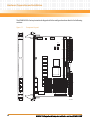
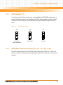
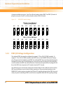
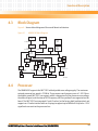
This chapter describes the MVME6100 on a block diagram level.
4.2
Features
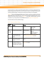
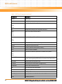
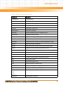
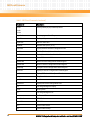
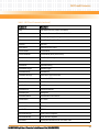
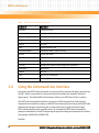
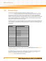
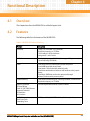
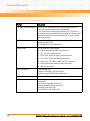
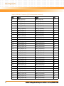
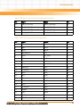
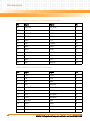
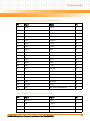
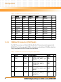
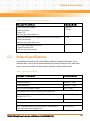
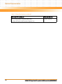
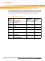
The following table lists the features of the MVME6100.
Table 4-1 MVME6100 Features Summary
Feature
Description
Processor
— Single 1.267 GHz MPC7457 processor
— Bus clock frequency at 133 MHz
— 36-bit address, 64-bit data buses
— Integrated L1 and L2 cache
L3 Cache
— Bus clock frequency at 211 MHz (when supported by processor)
— Up to 2MB using DDR SRAM
Flash
— Two banks (A & B) of soldered Intel StrataFlash devices
— 8 to 64MB supported on each bank
— Boot bank is switch selectable between banks
— Bank A has combination of software and hardware write-protect
scheme
— Bank B top 1MB block can be write-protected through
software/hardware write-protect control
System Memory
— Two banks on board for up to 1Gb using 256Mb or 512Mb devices
— Bus clock frequency at 133 MHz
Memory Controller
PCI Host Bridge
Dual 10/100/1000 Ethernet
Interrupt Controller
PCI Interface
I2C Interface
— Provided by Marvell MV64360 system controller
NVRAM
Real-Time Clock
Watchdog Timer
— 32KB provided by MK48T37 with SnapHat battery backup
MVME6100 Single Board Computer Installation and Use (6806800D58E)
59